JP7008808B2 - Manufacturing methods for semiconductor lasers and optoelectronic semiconductor components - Google Patents
Manufacturing methods for semiconductor lasers and optoelectronic semiconductor components Download PDFInfo
- Publication number
- JP7008808B2 JP7008808B2 JP2020519069A JP2020519069A JP7008808B2 JP 7008808 B2 JP7008808 B2 JP 7008808B2 JP 2020519069 A JP2020519069 A JP 2020519069A JP 2020519069 A JP2020519069 A JP 2020519069A JP 7008808 B2 JP7008808 B2 JP 7008808B2
- Authority
- JP
- Japan
- Prior art keywords
- protective cover
- laser
- facet
- adhesive
- semiconductor laser
- Prior art date
- Legal status (The legal status is an assumption and is not a legal conclusion. Google has not performed a legal analysis and makes no representation as to the accuracy of the status listed.)
- Active
Links
- 239000004065 semiconductor Substances 0.000 title claims description 86
- 230000005693 optoelectronics Effects 0.000 title claims description 14
- 238000004519 manufacturing process Methods 0.000 title claims description 13
- 230000001681 protective effect Effects 0.000 claims description 123
- 239000000853 adhesive Substances 0.000 claims description 75
- 230000001070 adhesive effect Effects 0.000 claims description 75
- 230000005855 radiation Effects 0.000 claims description 70
- 238000000576 coating method Methods 0.000 claims description 46
- 239000011248 coating agent Substances 0.000 claims description 41
- 239000011521 glass Substances 0.000 claims description 36
- 238000000034 method Methods 0.000 claims description 25
- 238000004020 luminiscence type Methods 0.000 claims description 21
- 239000000463 material Substances 0.000 claims description 14
- 229910052751 metal Inorganic materials 0.000 claims description 12
- 239000002184 metal Substances 0.000 claims description 12
- 229920001296 polysiloxane Polymers 0.000 claims description 9
- 238000007789 sealing Methods 0.000 claims description 7
- 230000000181 anti-adherent effect Effects 0.000 claims description 6
- 230000001699 photocatalysis Effects 0.000 claims description 5
- KPUWHANPEXNPJT-UHFFFAOYSA-N disiloxane Chemical class [SiH3]O[SiH3] KPUWHANPEXNPJT-UHFFFAOYSA-N 0.000 claims description 4
- 239000010980 sapphire Substances 0.000 claims description 4
- 229910052594 sapphire Inorganic materials 0.000 claims description 4
- 239000000126 substance Substances 0.000 claims description 2
- 238000002310 reflectometry Methods 0.000 claims 1
- 229910052791 calcium Inorganic materials 0.000 description 10
- 239000010410 layer Substances 0.000 description 10
- 229910052712 strontium Inorganic materials 0.000 description 10
- 230000007613 environmental effect Effects 0.000 description 9
- 230000002829 reductive effect Effects 0.000 description 9
- 239000007789 gas Substances 0.000 description 8
- 239000000203 mixture Substances 0.000 description 7
- 229910052788 barium Inorganic materials 0.000 description 6
- 238000005304 joining Methods 0.000 description 6
- 230000003287 optical effect Effects 0.000 description 6
- BASFCYQUMIYNBI-UHFFFAOYSA-N platinum Chemical compound [Pt] BASFCYQUMIYNBI-UHFFFAOYSA-N 0.000 description 6
- 230000008569 process Effects 0.000 description 6
- OKTJSMMVPCPJKN-UHFFFAOYSA-N Carbon Chemical compound [C] OKTJSMMVPCPJKN-UHFFFAOYSA-N 0.000 description 5
- 238000013461 design Methods 0.000 description 5
- 238000004049 embossing Methods 0.000 description 5
- 238000005538 encapsulation Methods 0.000 description 5
- -1 polysiloxane Polymers 0.000 description 5
- GWEVSGVZZGPLCZ-UHFFFAOYSA-N Titan oxide Chemical compound O=[Ti]=O GWEVSGVZZGPLCZ-UHFFFAOYSA-N 0.000 description 4
- 239000011230 binding agent Substances 0.000 description 4
- 230000003197 catalytic effect Effects 0.000 description 4
- 230000006378 damage Effects 0.000 description 4
- 230000003993 interaction Effects 0.000 description 4
- 239000011368 organic material Substances 0.000 description 4
- 239000002994 raw material Substances 0.000 description 4
- QVGXLLKOCUKJST-UHFFFAOYSA-N atomic oxygen Chemical compound [O] QVGXLLKOCUKJST-UHFFFAOYSA-N 0.000 description 3
- 150000001875 compounds Chemical class 0.000 description 3
- 238000000151 deposition Methods 0.000 description 3
- 238000009792 diffusion process Methods 0.000 description 3
- 238000010438 heat treatment Methods 0.000 description 3
- 239000011159 matrix material Substances 0.000 description 3
- 238000002844 melting Methods 0.000 description 3
- 230000008018 melting Effects 0.000 description 3
- 238000012576 optical tweezer Methods 0.000 description 3
- 239000001301 oxygen Substances 0.000 description 3
- 229910052760 oxygen Inorganic materials 0.000 description 3
- 239000002245 particle Substances 0.000 description 3
- 239000004033 plastic Substances 0.000 description 3
- 229910052697 platinum Inorganic materials 0.000 description 3
- 229920000642 polymer Polymers 0.000 description 3
- 239000000843 powder Substances 0.000 description 3
- 229910052761 rare earth metal Inorganic materials 0.000 description 3
- 150000002910 rare earth metals Chemical group 0.000 description 3
- 238000007493 shaping process Methods 0.000 description 3
- 229910000679 solder Inorganic materials 0.000 description 3
- 238000003860 storage Methods 0.000 description 3
- XLYOFNOQVPJJNP-UHFFFAOYSA-N water Chemical compound O XLYOFNOQVPJJNP-UHFFFAOYSA-N 0.000 description 3
- 229910018072 Al 2 O 3 Inorganic materials 0.000 description 2
- 102100032047 Alsin Human genes 0.000 description 2
- 101710187109 Alsin Proteins 0.000 description 2
- XKRFYHLGVUSROY-UHFFFAOYSA-N Argon Chemical compound [Ar] XKRFYHLGVUSROY-UHFFFAOYSA-N 0.000 description 2
- IJGRMHOSHXDMSA-UHFFFAOYSA-N Atomic nitrogen Chemical compound N#N IJGRMHOSHXDMSA-UHFFFAOYSA-N 0.000 description 2
- 239000004593 Epoxy Substances 0.000 description 2
- KDLHZDBZIXYQEI-UHFFFAOYSA-N Palladium Chemical compound [Pd] KDLHZDBZIXYQEI-UHFFFAOYSA-N 0.000 description 2
- OAICVXFJPJFONN-UHFFFAOYSA-N Phosphorus Chemical compound [P] OAICVXFJPJFONN-UHFFFAOYSA-N 0.000 description 2
- 229910004283 SiO 4 Inorganic materials 0.000 description 2
- VYPSYNLAJGMNEJ-UHFFFAOYSA-N Silicium dioxide Chemical compound O=[Si]=O VYPSYNLAJGMNEJ-UHFFFAOYSA-N 0.000 description 2
- 238000009825 accumulation Methods 0.000 description 2
- 230000009471 action Effects 0.000 description 2
- 229910052799 carbon Inorganic materials 0.000 description 2
- 238000006243 chemical reaction Methods 0.000 description 2
- 239000000356 contaminant Substances 0.000 description 2
- 230000008021 deposition Effects 0.000 description 2
- JKWMSGQKBLHBQQ-UHFFFAOYSA-N diboron trioxide Chemical compound O=BOB=O JKWMSGQKBLHBQQ-UHFFFAOYSA-N 0.000 description 2
- 230000005684 electric field Effects 0.000 description 2
- 230000009477 glass transition Effects 0.000 description 2
- 239000010439 graphite Substances 0.000 description 2
- 229910002804 graphite Inorganic materials 0.000 description 2
- 229910052734 helium Inorganic materials 0.000 description 2
- 229930195733 hydrocarbon Natural products 0.000 description 2
- 150000002430 hydrocarbons Chemical class 0.000 description 2
- 239000012535 impurity Substances 0.000 description 2
- 229910010272 inorganic material Inorganic materials 0.000 description 2
- 239000011147 inorganic material Substances 0.000 description 2
- 239000007788 liquid Substances 0.000 description 2
- 229910052749 magnesium Inorganic materials 0.000 description 2
- 239000002159 nanocrystal Substances 0.000 description 2
- 229910052757 nitrogen Inorganic materials 0.000 description 2
- 125000002080 perylenyl group Chemical class C1(=CC=C2C=CC=C3C4=CC=CC5=CC=CC(C1=C23)=C45)* 0.000 description 2
- 238000007639 printing Methods 0.000 description 2
- 238000012545 processing Methods 0.000 description 2
- 239000002096 quantum dot Substances 0.000 description 2
- HBMJWWWQQXIZIP-UHFFFAOYSA-N silicon carbide Chemical compound [Si+]#[C-] HBMJWWWQQXIZIP-UHFFFAOYSA-N 0.000 description 2
- 229910010271 silicon carbide Inorganic materials 0.000 description 2
- 239000004408 titanium dioxide Substances 0.000 description 2
- 229910001020 Au alloy Inorganic materials 0.000 description 1
- 229910015902 Bi 2 O 3 Inorganic materials 0.000 description 1
- 239000004215 Carbon black (E152) Substances 0.000 description 1
- 229910052688 Gadolinium Inorganic materials 0.000 description 1
- 229910010199 LiAl Inorganic materials 0.000 description 1
- 229910019142 PO4 Inorganic materials 0.000 description 1
- 229910004298 SiO 2 Inorganic materials 0.000 description 1
- 229910010037 TiAlN Inorganic materials 0.000 description 1
- ATJFFYVFTNAWJD-UHFFFAOYSA-N Tin Chemical compound [Sn] ATJFFYVFTNAWJD-UHFFFAOYSA-N 0.000 description 1
- PRPAGESBURMWTI-UHFFFAOYSA-N [C].[F] Chemical compound [C].[F] PRPAGESBURMWTI-UHFFFAOYSA-N 0.000 description 1
- 239000000654 additive Substances 0.000 description 1
- 229910052784 alkaline earth metal Inorganic materials 0.000 description 1
- 150000001342 alkaline earth metals Chemical group 0.000 description 1
- 229910052782 aluminium Inorganic materials 0.000 description 1
- 229910052786 argon Inorganic materials 0.000 description 1
- 230000002238 attenuated effect Effects 0.000 description 1
- 230000004888 barrier function Effects 0.000 description 1
- 239000011324 bead Substances 0.000 description 1
- 230000015572 biosynthetic process Effects 0.000 description 1
- 229910000416 bismuth oxide Inorganic materials 0.000 description 1
- 239000002041 carbon nanotube Substances 0.000 description 1
- 229910021393 carbon nanotube Inorganic materials 0.000 description 1
- 239000003054 catalyst Substances 0.000 description 1
- 239000000919 ceramic Substances 0.000 description 1
- 238000001311 chemical methods and process Methods 0.000 description 1
- 125000001309 chloro group Chemical group Cl* 0.000 description 1
- GTDCAOYDHVNFCP-UHFFFAOYSA-N chloro(trihydroxy)silane Chemical class O[Si](O)(O)Cl GTDCAOYDHVNFCP-UHFFFAOYSA-N 0.000 description 1
- 238000005253 cladding Methods 0.000 description 1
- 229910017052 cobalt Inorganic materials 0.000 description 1
- 239000010941 cobalt Substances 0.000 description 1
- GUTLYIVDDKVIGB-UHFFFAOYSA-N cobalt atom Chemical compound [Co] GUTLYIVDDKVIGB-UHFFFAOYSA-N 0.000 description 1
- 238000005056 compaction Methods 0.000 description 1
- 238000000354 decomposition reaction Methods 0.000 description 1
- 239000007857 degradation product Substances 0.000 description 1
- 230000001419 dependent effect Effects 0.000 description 1
- 238000011161 development Methods 0.000 description 1
- TYIXMATWDRGMPF-UHFFFAOYSA-N dibismuth;oxygen(2-) Chemical compound [O-2].[O-2].[O-2].[Bi+3].[Bi+3] TYIXMATWDRGMPF-UHFFFAOYSA-N 0.000 description 1
- 239000006185 dispersion Substances 0.000 description 1
- 238000009826 distribution Methods 0.000 description 1
- 230000000694 effects Effects 0.000 description 1
- 239000004811 fluoropolymer Substances 0.000 description 1
- 229920002313 fluoropolymer Polymers 0.000 description 1
- ZHPNWZCWUUJAJC-UHFFFAOYSA-N fluorosilicon Chemical compound [Si]F ZHPNWZCWUUJAJC-UHFFFAOYSA-N 0.000 description 1
- 229910052733 gallium Inorganic materials 0.000 description 1
- 239000002223 garnet Substances 0.000 description 1
- 239000003292 glue Substances 0.000 description 1
- PCHJSUWPFVWCPO-UHFFFAOYSA-N gold Chemical compound [Au] PCHJSUWPFVWCPO-UHFFFAOYSA-N 0.000 description 1
- 229910052737 gold Inorganic materials 0.000 description 1
- 239000010931 gold Substances 0.000 description 1
- 239000003353 gold alloy Substances 0.000 description 1
- JUWSSMXCCAMYGX-UHFFFAOYSA-N gold platinum Chemical compound [Pt].[Au] JUWSSMXCCAMYGX-UHFFFAOYSA-N 0.000 description 1
- 150000004820 halides Chemical group 0.000 description 1
- 239000001307 helium Substances 0.000 description 1
- SWQJXJOGLNCZEY-UHFFFAOYSA-N helium atom Chemical compound [He] SWQJXJOGLNCZEY-UHFFFAOYSA-N 0.000 description 1
- 239000011261 inert gas Substances 0.000 description 1
- 230000001788 irregular Effects 0.000 description 1
- 230000031700 light absorption Effects 0.000 description 1
- 230000007774 longterm Effects 0.000 description 1
- 238000010309 melting process Methods 0.000 description 1
- 229910044991 metal oxide Inorganic materials 0.000 description 1
- 150000004706 metal oxides Chemical class 0.000 description 1
- 238000001465 metallisation Methods 0.000 description 1
- 150000002739 metals Chemical class 0.000 description 1
- 229910003465 moissanite Inorganic materials 0.000 description 1
- 229910052605 nesosilicate Inorganic materials 0.000 description 1
- 150000004767 nitrides Chemical class 0.000 description 1
- 239000005304 optical glass Substances 0.000 description 1
- 239000005416 organic matter Substances 0.000 description 1
- 150000004762 orthosilicates Chemical class 0.000 description 1
- 238000013021 overheating Methods 0.000 description 1
- TWNQGVIAIRXVLR-UHFFFAOYSA-N oxo(oxoalumanyloxy)alumane Chemical compound O=[Al]O[Al]=O TWNQGVIAIRXVLR-UHFFFAOYSA-N 0.000 description 1
- RVTZCBVAJQQJTK-UHFFFAOYSA-N oxygen(2-);zirconium(4+) Chemical compound [O-2].[O-2].[Zr+4] RVTZCBVAJQQJTK-UHFFFAOYSA-N 0.000 description 1
- 229910052763 palladium Inorganic materials 0.000 description 1
- 230000036961 partial effect Effects 0.000 description 1
- CSHWQDPOILHKBI-UHFFFAOYSA-N peryrene Natural products C1=CC(C2=CC=CC=3C2=C2C=CC=3)=C3C2=CC=CC3=C1 CSHWQDPOILHKBI-UHFFFAOYSA-N 0.000 description 1
- NBIIXXVUZAFLBC-UHFFFAOYSA-K phosphate Chemical compound [O-]P([O-])([O-])=O NBIIXXVUZAFLBC-UHFFFAOYSA-K 0.000 description 1
- 239000010452 phosphate Substances 0.000 description 1
- 239000011941 photocatalyst Substances 0.000 description 1
- 239000006223 plastic coating Substances 0.000 description 1
- 239000004417 polycarbonate Substances 0.000 description 1
- 229920000515 polycarbonate Polymers 0.000 description 1
- 229920001709 polysilazane Polymers 0.000 description 1
- 229920001343 polytetrafluoroethylene Polymers 0.000 description 1
- 239000004810 polytetrafluoroethylene Substances 0.000 description 1
- 230000003449 preventive effect Effects 0.000 description 1
- 239000011241 protective layer Substances 0.000 description 1
- 229910052703 rhodium Inorganic materials 0.000 description 1
- 239000010948 rhodium Substances 0.000 description 1
- MHOVAHRLVXNVSD-UHFFFAOYSA-N rhodium atom Chemical compound [Rh] MHOVAHRLVXNVSD-UHFFFAOYSA-N 0.000 description 1
- 239000000377 silicon dioxide Substances 0.000 description 1
- 239000013464 silicone adhesive Substances 0.000 description 1
- 238000005476 soldering Methods 0.000 description 1
- 125000006850 spacer group Chemical group 0.000 description 1
- 230000003595 spectral effect Effects 0.000 description 1
- 238000005507 spraying Methods 0.000 description 1
- 150000003464 sulfur compounds Chemical class 0.000 description 1
- 230000003746 surface roughness Effects 0.000 description 1
- 229910052714 tellurium Inorganic materials 0.000 description 1
- PORWMNRCUJJQNO-UHFFFAOYSA-N tellurium atom Chemical compound [Te] PORWMNRCUJJQNO-UHFFFAOYSA-N 0.000 description 1
- 150000003568 thioethers Chemical class 0.000 description 1
- MTPVUVINMAGMJL-UHFFFAOYSA-N trimethyl(1,1,2,2,2-pentafluoroethyl)silane Chemical compound C[Si](C)(C)C(F)(F)C(F)(F)F MTPVUVINMAGMJL-UHFFFAOYSA-N 0.000 description 1
- UONOETXJSWQNOL-UHFFFAOYSA-N tungsten carbide Chemical compound [W+]#[C-] UONOETXJSWQNOL-UHFFFAOYSA-N 0.000 description 1
- 238000003466 welding Methods 0.000 description 1
- 229910052727 yttrium Inorganic materials 0.000 description 1
- 229910001928 zirconium oxide Inorganic materials 0.000 description 1
Images


Classifications
-
- H—ELECTRICITY
- H01—ELECTRIC ELEMENTS
- H01S—DEVICES USING THE PROCESS OF LIGHT AMPLIFICATION BY STIMULATED EMISSION OF RADIATION [LASER] TO AMPLIFY OR GENERATE LIGHT; DEVICES USING STIMULATED EMISSION OF ELECTROMAGNETIC RADIATION IN WAVE RANGES OTHER THAN OPTICAL
- H01S5/00—Semiconductor lasers
- H01S5/02—Structural details or components not essential to laser action
- H01S5/022—Mountings; Housings
- H01S5/023—Mount members, e.g. sub-mount members
- H01S5/02325—Mechanically integrated components on mount members or optical micro-benches
-
- H—ELECTRICITY
- H01—ELECTRIC ELEMENTS
- H01S—DEVICES USING THE PROCESS OF LIGHT AMPLIFICATION BY STIMULATED EMISSION OF RADIATION [LASER] TO AMPLIFY OR GENERATE LIGHT; DEVICES USING STIMULATED EMISSION OF ELECTROMAGNETIC RADIATION IN WAVE RANGES OTHER THAN OPTICAL
- H01S5/00—Semiconductor lasers
- H01S5/02—Structural details or components not essential to laser action
- H01S5/028—Coatings ; Treatment of the laser facets, e.g. etching, passivation layers or reflecting layers
-
- H—ELECTRICITY
- H01—ELECTRIC ELEMENTS
- H01S—DEVICES USING THE PROCESS OF LIGHT AMPLIFICATION BY STIMULATED EMISSION OF RADIATION [LASER] TO AMPLIFY OR GENERATE LIGHT; DEVICES USING STIMULATED EMISSION OF ELECTROMAGNETIC RADIATION IN WAVE RANGES OTHER THAN OPTICAL
- H01S5/00—Semiconductor lasers
- H01S5/02—Structural details or components not essential to laser action
- H01S5/022—Mountings; Housings
- H01S5/0225—Out-coupling of light
- H01S5/02253—Out-coupling of light using lenses
-
- H—ELECTRICITY
- H01—ELECTRIC ELEMENTS
- H01S—DEVICES USING THE PROCESS OF LIGHT AMPLIFICATION BY STIMULATED EMISSION OF RADIATION [LASER] TO AMPLIFY OR GENERATE LIGHT; DEVICES USING STIMULATED EMISSION OF ELECTROMAGNETIC RADIATION IN WAVE RANGES OTHER THAN OPTICAL
- H01S5/00—Semiconductor lasers
- H01S5/02—Structural details or components not essential to laser action
- H01S5/022—Mountings; Housings
- H01S5/023—Mount members, e.g. sub-mount members
- H01S5/02325—Mechanically integrated components on mount members or optical micro-benches
- H01S5/02326—Arrangements for relative positioning of laser diodes and optical components, e.g. grooves in the mount to fix optical fibres or lenses
-
- H—ELECTRICITY
- H01—ELECTRIC ELEMENTS
- H01S—DEVICES USING THE PROCESS OF LIGHT AMPLIFICATION BY STIMULATED EMISSION OF RADIATION [LASER] TO AMPLIFY OR GENERATE LIGHT; DEVICES USING STIMULATED EMISSION OF ELECTROMAGNETIC RADIATION IN WAVE RANGES OTHER THAN OPTICAL
- H01S5/00—Semiconductor lasers
- H01S5/02—Structural details or components not essential to laser action
- H01S5/022—Mountings; Housings
- H01S5/0235—Method for mounting laser chips
- H01S5/02355—Fixing laser chips on mounts
- H01S5/0236—Fixing laser chips on mounts using an adhesive
-
- H—ELECTRICITY
- H01—ELECTRIC ELEMENTS
- H01S—DEVICES USING THE PROCESS OF LIGHT AMPLIFICATION BY STIMULATED EMISSION OF RADIATION [LASER] TO AMPLIFY OR GENERATE LIGHT; DEVICES USING STIMULATED EMISSION OF ELECTROMAGNETIC RADIATION IN WAVE RANGES OTHER THAN OPTICAL
- H01S5/00—Semiconductor lasers
- H01S5/005—Optical components external to the laser cavity, specially adapted therefor, e.g. for homogenisation or merging of the beams or for manipulating laser pulses, e.g. pulse shaping
- H01S5/0078—Optical components external to the laser cavity, specially adapted therefor, e.g. for homogenisation or merging of the beams or for manipulating laser pulses, e.g. pulse shaping for frequency filtering
-
- H—ELECTRICITY
- H01—ELECTRIC ELEMENTS
- H01S—DEVICES USING THE PROCESS OF LIGHT AMPLIFICATION BY STIMULATED EMISSION OF RADIATION [LASER] TO AMPLIFY OR GENERATE LIGHT; DEVICES USING STIMULATED EMISSION OF ELECTROMAGNETIC RADIATION IN WAVE RANGES OTHER THAN OPTICAL
- H01S5/00—Semiconductor lasers
- H01S5/005—Optical components external to the laser cavity, specially adapted therefor, e.g. for homogenisation or merging of the beams or for manipulating laser pulses, e.g. pulse shaping
- H01S5/0087—Optical components external to the laser cavity, specially adapted therefor, e.g. for homogenisation or merging of the beams or for manipulating laser pulses, e.g. pulse shaping for illuminating phosphorescent or fluorescent materials, e.g. using optical arrangements specifically adapted for guiding or shaping laser beams illuminating these materials
Landscapes
- Physics & Mathematics (AREA)
- Condensed Matter Physics & Semiconductors (AREA)
- General Physics & Mathematics (AREA)
- Electromagnetism (AREA)
- Optics & Photonics (AREA)
- Semiconductor Lasers (AREA)
- Mounting And Adjusting Of Optical Elements (AREA)
Description
半導体レーザが提供される。さらに、オプトエレクトロニクス半導体部品のための製造方法が提供される。 Semiconductor lasers are provided. In addition, manufacturing methods for optoelectronic semiconductor components are provided.
実現される目的は、効率的に封止することができ、効率的に製造することができるオプトエレクトロニクス半導体部品を提供することである。 An object to be realized is to provide optoelectronic semiconductor components that can be efficiently sealed and efficiently manufactured.
この目的は、とりわけ、独立クレームの特徴を有する半導体レーザおよび製造方法によって実現される。好ましい発展形態は、従属クレームの主題である。 This purpose is achieved, among other things, by semiconductor lasers and manufacturing methods that feature independent claims. A preferred form of development is the subject of dependent claims.
少なくとも1つの実施形態によれば、半導体レーザは、キャリアを含む。キャリアは、いわゆるサブマウントであってよい。キャリアは、半導体レーザを制御することができるドライバーを含むことが可能である。あるいは、キャリアは、電子的にパッシブな構成要素を表し、実装面としてだけ使用されることが可能である。 According to at least one embodiment, the semiconductor laser comprises a carrier. The carrier may be a so-called submount. The carrier can include a driver capable of controlling the semiconductor laser. Alternatively, the carrier represents an electronically passive component and can only be used as a mounting surface.
少なくとも1つの実施形態によれば、半導体レーザは、1つ以上のレーザダイオードを含む。この少なくとも1つのレーザダイオードは、好ましくは、端面発光型レーザダイオードである。これは、特に、動作時に発生したレーザ放射は、レーザダイオードの活性領域に平行な方向に放出されることを意味する。 According to at least one embodiment, the semiconductor laser comprises one or more laser diodes. The at least one laser diode is preferably an end face emitting laser diode. This means that, in particular, the laser emission generated during operation is emitted in a direction parallel to the active region of the laser diode.
少なくとも1つの実施形態によれば、レーザダイオードは、ファセットを含む。ファセットは、好ましくは、活性領域に対して垂直またはほぼ垂直に配向している。ファセット上に放射出口領域が配置される。動作時に発生するレーザ放射は、放射出口領域においてレーザダイオードから出現する。放射出口領域は、特に、ファセットの部分領域に、従ってファセットに限定される。 According to at least one embodiment, the laser diode comprises a facet. The facets are preferably oriented perpendicular or nearly perpendicular to the active region. A radiation outlet area is placed on the facet. The laser emission generated during operation emerges from the laser diode in the emission outlet region. The radiation outlet area is particularly limited to the facet subregion, and thus to the facet.
少なくとも1つの実施形態によれば、半導体レーザは、1つ以上の保護カバー、特に、ちょうど1つの保護カバーを含む。保護カバーは、好ましくは、光線整形または光線偏向のための光学機器であるが、ディスク、例えば面平行プレートなどの光学不活性体でもあってよい。 According to at least one embodiment, the semiconductor laser comprises one or more protective covers, in particular just one protective cover. The protective cover is preferably an optical instrument for ray shaping or ray deflection, but may also be an optically inactive material such as a disk, eg, a plane parallel plate.
特に、保護カバーは、好ましくは、発生する放射のコリメーションまたは集束のために設計されるレンズである。レンズは、球面、非球面、または自由形状の形であってよい。さらに、円筒形レンズまたは半円筒形レンズが可能である。保護カバーは、収束レンズであり得る。保護カバーは、例えば、平凸レンズまたは両凸レンズとして設計されてよい。フレネルレンズとしての実施形態も可能である。さらに、保護カバーは、例えば、ビーム偏向用のプリズムであってよい。 In particular, the protective cover is preferably a lens designed for the collimation or focusing of the generated radiation. The lens may be spherical, aspherical, or free-form. Further, a cylindrical lens or a semi-cylindrical lens is possible. The protective cover can be a convergent lens. The protective cover may be designed, for example, as a plano-convex lens or a biconvex lens. An embodiment as a Fresnel lens is also possible. Further, the protective cover may be, for example, a prism for beam deflection.
少なくとも1つの実施形態によれば、保護カバーは、ガラスまたはサファイヤまたはSiCなどの無機材料でできている。あるいは、あまり好ましくはないが、保護カバーは、プラスチック、例えばシリコーンもしくはエポキシまたはそれらのハイブリッド材料などの有機材料、あるいは、ポリカーボネートなどのポリマーでできている。保護カバーが有機材料でできている場合、この有機材料は、好ましくは、保護カバーの芯を形成し、芯は、例えば、酸素および/または水蒸気に対する拡散障壁としての無機保護層によって、特に、表面全体にわたって周りをすべて覆われてよい。 According to at least one embodiment, the protective cover is made of glass or an inorganic material such as sapphire or SiC. Alternatively, less preferably, the protective cover is made of a plastic, such as an organic material such as silicone or epoxy or a hybrid material thereof, or a polymer such as polycarbonate. If the protective cover is made of an organic material, this organic material preferably forms the core of the protective cover, which is particularly surfaced by, for example, an inorganic protective layer as a diffusion barrier to oxygen and / or water vapor. All around may be covered throughout.
少なくとも1つの実施形態によれば、半導体レーザは、接着剤を含む。保護カバーは、接着剤を用いてファセットに、および任意選択としてキャリアの側面に取り付けられる。キャリアの側面は、ファセットに平行またはほぼ平行に配向してよい。キャリアの側面は、好ましくは、レーザ放射の光線方向に沿ってファセットより後退している。従って、保護カバーは、好ましくは、接着剤でファセットおよびキャリアに取り付けられる。接着剤は、好ましくは、ガラスまたは少なくとも1種類の金属などの無機材料である。 According to at least one embodiment, the semiconductor laser comprises an adhesive. The protective cover is attached to the facet using adhesive and, optionally, to the sides of the carrier. The sides of the carrier may be oriented parallel to or nearly parallel to the facet. The sides of the carrier preferably recede from the facet along the direction of the laser beam. Therefore, the protective cover is preferably attached to the facet and carrier with an adhesive. The adhesive is preferably an inorganic material such as glass or at least one metal.
あるいは、接着剤は、シリコーン、ポリシロキサン、ポリシラザンまたはシリコーンハイブリッド材料、好ましくは低有機プラスチックなどのプラスチックである。ポリシロキサンとは、材料が-[O-SiR2]n-、ポリシラザンの場合は-[NH-SiR2]n-で構築されることを意味する。ここで、各々の場合に異なる部分Rが存在することが可能である。低有機とは、例えば、シリコーン、シロキサンまたはシラザンに対する有機成分の割合が、30質量%または20質量%を超えず、および/または、特に、シロキサンまたはシラザンの場合、炭素含有部分Rの数とnとの商が多くとも0.75または0.25であることを意味する。有機物の質量割合は、特に、材料を灰化することによって決定される。 Alternatively, the adhesive is a plastic such as silicone, polysiloxane, polysilazane or a silicone hybrid material, preferably a low organic plastic. Polysiloxane means that the material is constructed of-[O-SiR 2 ] n- , and in the case of polysilazane- [NH-SiR 2 ] n- . Here, it is possible that different portions R may exist in each case. Low organic means, for example, that the ratio of organic components to silicone, siloxane or silazane does not exceed 30% by weight or 20% by weight and / or, especially in the case of siloxane or silazane, the number of carbon-containing moieties R and n. It means that the quotient with is at most 0.75 or 0.25. The mass percentage of organic matter is determined, in particular, by incineration of the material.
あまり好ましくはないが、接着剤は、エポキシおよび/または炭素含有構造単位のポリマーなどの有機材料であり得る。 Although less preferred, the adhesive can be an organic material such as an epoxy and / or a polymer of carbon-containing structural units.
少なくとも1つの実施形態によれば、保護カバーの光入射面とファセットとの間の平均距離は、多くとも5μmまたは15μmまたは30μmまたは60μmまたは0.1mmである、あるいは、または加えて、この平均距離は、少なくとも0.1μmまたは0.5μmである。平均距離は、好ましくは、0.5μmから5μmの間の範囲にある。言い換えると、保護カバーは、ファセットの近くであり得る。 According to at least one embodiment, the average distance between the light incident surface of the protective cover and the facet is at most 5 μm or 15 μm or 30 μm or 60 μm or 0.1 mm, or in addition, this average distance. Is at least 0.1 μm or 0.5 μm. The average distance is preferably in the range of 0.5 μm to 5 μm. In other words, the protective cover can be near the facet.
少なくとも1つの実施形態によれば、半導体レーザは、通常雰囲気中で追加の気密封止なく動作するように構成される。すなわち、ファセットの、特に放射出口領域の封止および保護は、保護カバーと一緒になった接着剤によって行われる。保護カバーと一緒になった接着剤に起因して、半導体レーザは、好ましくは、通常の環境空気中で動作させてよく、環境空気は、21%前後の範囲の酸素含有量および水蒸気を含有してよい。 According to at least one embodiment, the semiconductor laser is configured to operate in a normal atmosphere without additional airtight sealing. That is, the sealing and protection of the facets, especially the radiation outlet area, is done by the adhesive combined with the protective cover. Due to the adhesive combined with the protective cover, the semiconductor laser may preferably be operated in normal environmental air, which contains oxygen content and water vapor in the range of around 21%. It's okay.
少なくとも1つの実施形態において、半導体レーザは、キャリアと、キャリアに実装されレーザ放射を発生するための活性領域および放射出口領域を有するファセットを含む端面発光型レーザダイオードと、を含む。半導体レーザは、さらに、保護カバー、好ましくは、レーザ放射を平行にするためのレンズを含む。保護カバーは、接着剤を用いてファセットおよびキャリアの側面に固定される。保護カバーの光入射面とファセットとの間の平均距離は、多くとも60μmである。半導体レーザは、通常雰囲気中で追加の気密封止なく動作するように構成される。 In at least one embodiment, the semiconductor laser comprises a carrier and an end face emitting laser diode including a facet mounted on the carrier and having an active region and a radiation exit region for generating laser radiation. The semiconductor laser further includes a protective cover, preferably a lens for parallelizing the laser emission. The protective cover is secured to the sides of the facet and carrier using adhesive. The average distance between the light incident surface of the protective cover and the facets is at most 60 μm. Semiconductor lasers are usually configured to operate in an atmosphere without additional airtight seals.
特に、高い出力、例えば0.2Wまたは1Wを超える光出力を有し、近紫外域または青色スペクトル域の短波長で放出する半導体レーザは、環境の影響に対して保護され、封止されなければならない。長期間の安定な動作を確実にすることを可能にするために、対応するレーザダイオードは、清浄で気密に密封された雰囲気中で動作させるか、またはあらゆる雰囲気から遠ざけなければならない。 In particular, semiconductor lasers that have high power output, eg, light output greater than 0.2 W or 1 W, and emit at short wavelengths in the near-ultraviolet or blue spectral range must be protected and sealed against environmental influences. It doesn't become. Corresponding laser diodes must be operated in a clean, airtight and sealed atmosphere or kept away from any atmosphere to ensure long-term stable operation.
本明細書に記載される半導体レーザにおいて、ファセットの近くにあるクラッドを用いて放射出口領域の気密区画形成が行われる。接着剤と一緒になった保護カバーによって形成されたファセットの近くでの封止によって、その他の方法では必要となる気密に密封されたハウジングをなくすことができる。その結果、半導体レーザは、コスト効率を改善して製造することができ、スペース要件を軽減して設置することができる。 In the semiconductor lasers described herein, an airtight compartment is formed in the radiation outlet region using a cladding near the facet. Sealing near the facets formed by a protective cover with adhesive can eliminate the airtightly sealed housing that would otherwise be required. As a result, semiconductor lasers can be manufactured with improved cost efficiency and can be installed with reduced space requirements.
保護カバーは、特に、接着剤と一緒になると、環境の影響に対してファセットを保護し、レーザ放射の光線発散を減らす。同様に、例えばレンズの形の保護カバーを用いると、生じ得る分解生成物が堆積することができる表面の拡大がもたらされる。さらに、雰囲気に曝露されている半導体レーザの表面の拡大は、光出力密度の低下という結果を生み、光ピンセットの効果の低下を伴う。特に、保護カバーは、レーザファセットおよび放射出口領域に粒子および/または無機分子が直接集積することを防ぐ。 The protective cover, especially when combined with adhesive, protects the facet against environmental influences and reduces the emission of laser radiation. Similarly, for example, the use of a protective cover in the form of a lens results in an enlargement of the surface on which possible degradation products can be deposited. In addition, enlargement of the surface of the semiconductor laser exposed to the atmosphere results in a decrease in light output density, accompanied by a decrease in the effectiveness of the optical tweezers. In particular, the protective cover prevents the direct accumulation of particles and / or inorganic molecules in the laser facet and radiation outlet regions.
ファセット上の堆積物は、特に、短波長放射によって分解することができ、焼き付かせることができる。ファセットの領域におけるそのような変化は、レーザのデカップリング効率を低下させ、例えば、堆積物中の光吸収によるファセットコーティングへの損傷が起こり、そのことが今度は、過熱、ひいてはレーザファセット領域全体の破壊につながりかねない。これは、光学損傷、略してCOD(catastrophic optical damage)とも呼ばれる。ファセット領域に実装された保護カバーは、粒子および/または分子がファセットに堆積することを防ぐ一方で、同時に半導体レーザの構成を単純にし、スペース要件を軽減する。 The deposits on the facet can be decomposed and burned, in particular by short wavelength radiation. Such changes in the facet region reduce the decoupling efficiency of the laser, for example, damage to the facet coating due to light absorption in the deposit, which in turn causes overheating and thus the entire laser facet region. It can lead to destruction. This is also referred to as optical damage, or COD (catalytic optical damage) for short. The protective cover mounted in the facet region prevents particles and / or molecules from depositing on the facet, while at the same time simplifying the configuration of the semiconductor laser and reducing space requirements.
さらに、放出されるレーザ放射の発散は、ファセットに近いレンズによって低下する。同様に、雰囲気中を通るレーザ光線の領域における電界強度は、低下する。発散光線中の電界強度は、さもなければファセットの近傍において潜在的な汚染物を吸引し、光ピンセットに対応するファセットへの堆積を引き起こす。このようにして、光線発散の低下は、堆積物の減少に直接つながる。 In addition, the divergence of the emitted laser radiation is reduced by the lens closer to the facet. Similarly, the electric field strength in the region of the laser beam passing through the atmosphere is reduced. The electric field strength in the divergent light otherwise attracts potential contaminants in the vicinity of the facets, causing deposition on the facets corresponding to the optical tweezers. In this way, reduced light emission directly leads to reduced deposits.
さらに、保護カバーによって、すなわち、好ましくはレンズによって、雰囲気との界面が拡大する。境界表面の拡大の結果として、単位面積あたりの潜在的堆積物の量は、減少する。さらに、この界面におけるエネルギー密度は、ファセットに関して直接低下する。 In addition, the protective cover, preferably the lens, expands the interface with the atmosphere. As a result of the expansion of the boundary surface, the amount of potential deposits per unit area is reduced. In addition, the energy density at this interface drops directly with respect to facets.
少なくとも1つの実施形態によれば、レーザダイオードは、接着剤および保護カバーによって気密封止される。すなわち、保護カバーとともに接着剤から形成された封止部の内部と外部との間に、酸素または水蒸気などの物質の有意な交換がない。例えば、気密に密封されるとは、特に室温において、漏洩速度が多くとも5×10⁻⁹Pa・m/sであることを意味する。 According to at least one embodiment, the laser diode is hermetically sealed with an adhesive and a protective cover. That is, there is no significant exchange of substances such as oxygen or water vapor between the inside and outside of the encapsulation formed from the adhesive along with the protective cover. For example, airtight sealing means that the leakage rate is at most 5 × 10⁻⁹ Pa · m / s, especially at room temperature.
少なくとも1つの実施形態によれば、保護カバーとファセットとの間の最小距離は、0.1μmまたは0.2μmである。あるいは、または加えて、この最小距離は、多くとも10μmまたは5μmまたは3μmである。すなわち、最小距離は、レーザ放射の波長のオーダーであり得る。その結果、保護カバーとファセットとの間の領域が、望ましくない追加の共振器としての役割を果たす可能性がある。他方、この小さな最小距離は、放射出口領域の方へ、特に接着剤を通って、小さな拡散断面積しか発生しないという結果を生む。 According to at least one embodiment, the minimum distance between the protective cover and the facets is 0.1 μm or 0.2 μm. Alternatively, or in addition, this minimum distance is at most 10 μm or 5 μm or 3 μm. That is, the minimum distance can be on the order of the wavelength of the laser emission. As a result, the area between the protective cover and the facet can act as an unwanted additional resonator. On the other hand, this small minimum distance results in a small diffusion cross section towards the radiation outlet region, especially through the adhesive.
少なくとも1つの実施形態によれば、活性領域の領域中のファセット上にキャビティが形成される。ファセットの平面図で見ると、キャビティは、接着剤によって周りをすべて囲まれている。従って、レーザ放射がレーザダイオードを離れる放射出口領域は、接着剤なしでよい。このことは、レーザ放射と接着剤との間で放射出口領域において直ちに潜在的に有害な相互作用があるという結果を生まない。 According to at least one embodiment, cavities are formed on the facets in the region of the active region. Looking at the facet plan, the cavity is all surrounded by glue. Therefore, the radiation outlet region where the laser emission leaves the laser diode may be adhesive-free. This does not result in immediate and potentially harmful interactions between the laser radiation and the adhesive in the radiation outlet region.
少なくとも1つの実施形態によれば、キャビティは、排気されるか、または1種類以上の保護ガスで満たされる。該当する保護ガスは、例えば、アルゴンもしくはヘリウムなどの希ガスまたは窒素などの不活性ガスである。キャビティが保護ガスで満たされる場合、キャビティ中のガス圧力は、例えば、半導体レーザの意図される動作温度において大気圧に近く、特に0.8バール以上から1.1バール以下の間であってよい。 According to at least one embodiment, the cavity is either exhausted or filled with one or more protective gases. The applicable protective gas is, for example, a rare gas such as argon or helium or an inert gas such as nitrogen. When the cavity is filled with protective gas, the gas pressure in the cavity may be, for example, close to atmospheric pressure at the intended operating temperature of the semiconductor laser, especially between 0.8 bar and above and 1.1 bar and below. ..
少なくとも1つの実施形態によれば、キャビティの平均直径は、ファセットの平面図で見ると、少なくとも3μmまたは5μmまたは10μmおよび/または多くとも0.1mmまたは50μmまたは20μmまたは10μmである。言い換えると、キャビティは、平面図で見ると、比較的小さくてよい。 According to at least one embodiment, the average diameter of the cavity is at least 3 μm or 5 μm or 10 μm and / or at most 0.1 mm or 50 μm or 20 μm or 10 μm when viewed in plan view of the facets. In other words, the cavity may be relatively small when viewed in plan view.
キャビティは、放射出口領域に対して回転対称的に形成されるか、または放射出口領域の周りに非対称に延在してよい。接着剤と放射出口領域との間の距離は、好ましくは、少なくとも2μmまたは5μmまたは10μmである。 The cavity may be formed rotationally symmetric with respect to the radiation exit region or may extend asymmetrically around the radiation outlet region. The distance between the adhesive and the radiation outlet region is preferably at least 2 μm or 5 μm or 10 μm.
少なくとも1つの実施形態によれば、キャビティの厚さは、0.5μm以上から20μm以下の間である。ファセットに垂直なキャビティの厚さは、一方では放射出口領域および/またはキャリアの側面と他方では保護カバーの光入射面との間の平均距離に対応してよい。 According to at least one embodiment, the thickness of the cavity is between 0.5 μm and above and 20 μm and below. The thickness of the cavity perpendicular to the facet may correspond to the average distance between the radiation outlet region and / or the side of the carrier on the one hand and the light incident surface of the protective cover on the other.
少なくとも1つの実施形態によれば、ファセットの平面図で見ると、キャビティの周りの接着剤の幅は、キャビティの平均直径の少なくとも100%または150%または250%である。あるいは、または加えて、接着剤の幅は、少なくとも20μmまたは30μmまたは50μmおよび/または多くとも0.1mmまたは50μmまたは20μmである。 According to at least one embodiment, when viewed in plan view of the facet, the width of the adhesive around the cavity is at least 100%, 150% or 250% of the average diameter of the cavity. Alternatively, or in addition, the width of the adhesive is at least 20 μm or 30 μm or 50 μm and / or at most 0.1 mm or 50 μm or 20 μm.
少なくとも1つの実施形態によれば、キャビティの側壁は、接着剤の方へ湾曲している。例えば、ファセットに垂直な断面で見ると、キャビティの形は、放射出口領域において両凸である。すなわち、この断面図で見てファセットに平行な方向の最大限度から始まり、キャビティは、ファセットに向かう方向および保護カバーの光入射面に向かう方向で狭くなる。 According to at least one embodiment, the sidewalls of the cavity are curved towards the adhesive. For example, when viewed in cross section perpendicular to the facet, the shape of the cavity is biconvex in the radiation outlet region. That is, starting from the maximum in the direction parallel to the facet as seen in this cross section, the cavity narrows in the direction toward the facet and in the direction toward the light incident surface of the protective cover.
少なくとも1つの実施形態によれば、レーザ放射は、接着剤からある距離をおいて光入射面へと通る。すなわち、放射出口領域から光入射面への直進的な意図される経路に沿って、レーザ放射は、接着剤に到達しない。これは、場合によって光入射面において反射したレーザ放射が接着剤に導かれることを除外しない。 According to at least one embodiment, the laser emission passes to the light incident surface at a distance from the adhesive. That is, the laser emission does not reach the adhesive along the intended path straight from the emission exit region to the light incident surface. This does not exclude that the laser radiation reflected at the light incident surface is sometimes guided to the adhesive.
少なくとも1つの実施形態によれば、接着剤は、光入射面および任意選択としてキャリアの側面を部分的にまたは完全に覆い、放射出口領域全体の上も直接かつ直ちに覆う。言い換えると、ファセットと光入射面との間の接着剤によってのみ連続的でかつ間隙のない接続を形成することができる。 According to at least one embodiment, the adhesive partially or completely covers the light incident surface and optionally the sides of the carrier and also directly and immediately over the entire radiation outlet region. In other words, a continuous and gapless connection can only be formed by the adhesive between the facet and the light incident surface.
少なくとも1つの実施形態によれば、光入射面は、全体が接着剤によって覆われる。同様に、ファセットは、全体が接着剤によって覆われ得る。キャリアの側面は、好ましくは、部分的にしか接着剤によって覆われないが、あるいは接着剤によって完全に覆われてもよい。 According to at least one embodiment, the light incident surface is entirely covered with an adhesive. Similarly, the facet can be entirely covered with adhesive. The sides of the carrier are preferably only partially covered by the adhesive, or may be completely covered by the adhesive.
少なくとも1つの実施形態によれば、保護カバーと接着剤との間の屈折率の差は、多くとも0.2または0.1または0.05または0.02である。これは、詳しくは、レーザ放射の最大強度の波長において300Kの温度であてはまる。対応して低い屈折率差によって保護カバーと接着剤との間の界面における反射を低下させることができる。 According to at least one embodiment, the difference in refractive index between the protective cover and the adhesive is at most 0.2 or 0.1 or 0.05 or 0.02. This specifically applies at a temperature of 300 K at the wavelength of the maximum intensity of the laser emission. A correspondingly low index of refraction difference can reduce reflections at the interface between the protective cover and the adhesive.
少なくとも1つの実施形態によれば、保護カバーは、以下の材料、ガラス、サファイヤ、炭化ケイ素のうちの少なくとも1種類でできているか、またはこれらの材料の1種類以上からなる。保護カバーは、好ましくは、サファイヤでできている。 According to at least one embodiment, the protective cover is made of at least one of the following materials, glass, sapphire, silicon carbide, or one or more of these materials. The protective cover is preferably made of sapphire.
少なくとも1つの実施形態によれば、レーザダイオードによって発生するレーザ放射の最大強度の波長は、少なくとも365nmまたは400nmである。あるいは、または加えて、最大強度の波長は、多くとも530nmまたは460nmまたは440nmである。すなわち、レーザ放射は、比較的短波長である。 According to at least one embodiment, the wavelength of the maximum intensity of the laser emission generated by the laser diode is at least 365 nm or 400 nm. Alternatively, or in addition, the wavelength of maximum intensity is at most 530 nm or 460 nm or 440 nm. That is, the laser emission has a relatively short wavelength.
少なくとも1つの実施形態によれば、接着剤は、1種類以上の金属、特にハンダからなり、ハンダが施用される保護カバーおよび/またはファセットおよび側面の上の金属層とも組合される。あるいは、少なくとも1種類のガラスが接着剤として用いられる。 According to at least one embodiment, the adhesive consists of one or more metals, in particular solder, and is also combined with a protective cover and / or a metal layer on the facet and sides to which the solder is applied. Alternatively, at least one type of glass is used as the adhesive.
接着剤は、均一な構成であってもよく、不均一であってもよい。例えば、ガラスの場合、例えばスペーサとして、および/または熱膨脹率を設定するために、さらに別の粒子がガラスマトリックス中に導入されることが可能である。 The adhesive may have a uniform composition or may be non-uniform. For example, in the case of glass, yet another particle can be introduced into the glass matrix, for example as a spacer and / or to set the thermal expansion rate.
少なくとも1つの実施形態によれば、保護カバーの光入射面に粗面化部が設けられる。光入射面は、従って、光入射面で反射した放射を、反射したレーザ放射が放射出口領域に届かないかまたは減衰されてからしか届かないほど広範囲に拡散させるように設計される。ファセットと保護カバーとの間の領域からレーザダイオードの共振器へのフィードバックは、従って、低下させることができる。 According to at least one embodiment, a roughened portion is provided on the light incident surface of the protective cover. The light-incident surface is therefore designed to diffuse the radiation reflected by the light-incident surface so extensively that the reflected laser radiation does not reach the emission exit region or only after it has been attenuated. The feedback from the region between the facet to the protective cover to the resonator of the laser diode can therefore be reduced.
少なくとも1つの実施形態によれば、光入射面は平らである。この場合、光入射面は、ファセットに対して斜めになる。例えば、光入射面とファセットとの間の角度は、少なくとも5°または10°、および/または多くとも35°または25°または15°である。その結果、光入射面で反射したレーザ放射は、ファセット上の放射出口領域から遠ざけられる。その角度は、好ましくは、接着剤上の拡散攻撃の面積を低く保つために、ブリュースター角未満である。 According to at least one embodiment, the light incident surface is flat. In this case, the light incident surface is slanted with respect to the facet. For example, the angle between the light incident surface and the facet is at least 5 ° or 10 ° and / or at most 35 ° or 25 ° or 15 °. As a result, the laser radiation reflected by the light incident surface is kept away from the radiation outlet region on the facet. The angle is preferably less than the Brewster angle in order to keep the area of diffusion attack on the adhesive low.
少なくとも1つの実施形態によれば、保護カバーは、光入射面が湾曲した形で、特に連続的に湾曲した形で延在するように、レンズの形であり両凸である。光入射面の最大湾曲部は、好ましくは、場合によって光入射面において反射したあらゆるレーザ放射を放射出口領域から遠ざけるように、レーザ放射の光軸の外側に配置される。 According to at least one embodiment, the protective cover is in the form of a lens and biconvex so that the light incident surface extends in a curved shape, especially in a continuously curved shape. The maximum curvature of the light incident surface is preferably located outside the optical axis of the laser radiation so as to keep any laser radiation reflected at the light incident surface away from the radiation exit region.
少なくとも1つの実施形態によれば、保護カバーの光入射面および/または光出射面に、部分的にまたは全体的にレーザ放射のための反射防止コーティングが設けられる。詳しくは、レーザ放射に対する光入射面の反射率は、多くとも0.5%または0.1%または0.01%である。そのような反射防止コーティングによってファセットと保護カバーとの間の領域からレーザダイオードの共振器へのフィードバックも低下させるかまたは妨ぐことができる。 According to at least one embodiment, the light-incident and / or light-emitting surfaces of the protective cover are provided with an antireflection coating for laser emission, partially or entirely. Specifically, the reflectance of the light incident surface with respect to laser radiation is at most 0.5%, 0.1% or 0.01%. Such antireflection coatings can also reduce or prevent feedback of the laser diode from the area between the facet and the protective cover to the resonator.
少なくとも1つの実施形態によれば、ファセットとは反対側の保護カバーの光出射面に触媒コーティング、好ましくは光触媒コーティングが設けられる。このコーティングは、レーザ放射を用いて光出射面上の堆積物を除去および/または分解するように設計されている。コーティングは、特に、二酸化チタンまたは酸化ジルコニウムなどの金属酸化物によって形成される。あるいは、コーティングは、白金またはパラジウムまたはロジウムなどの少なくとも1種類の金属でできている。触媒コーティング用の金属コーティングの場合、コーティングの厚さは、好ましくは、多くとも10nmまたは5nmまたは3nmであり、それによって、レーザ放射は、顕著な損失なく触媒コーティングを通過することができる。 According to at least one embodiment, a catalytic coating, preferably a photocatalytic coating, is provided on the light emitting surface of the protective cover opposite the facet. This coating is designed to remove and / or decompose deposits on the light emitting surface using laser radiation. The coating is specifically formed from metal oxides such as titanium dioxide or zirconium oxide. Alternatively, the coating is made of at least one metal such as platinum or palladium or rhodium. For metal coatings for catalytic coatings, the coating thickness is preferably at most 10 nm or 5 nm or 3 nm so that laser radiation can pass through the catalytic coating without significant loss.
少なくとも1つの実施形態によれば、保護カバーの光出射面に接着防止コーティングが設けられる。接着防止コーティングは、保護カバーの外側における堆積物を防ぐように設計されている。接着防止コーティングは、例えば、プラスチックコーティングであり、特に、フッ素-炭素化合物またはフッ素-ケイ素化合物を有する。接着防止コーティングは、例えば、フッ素化もしくは過フッ素化ポリマーおよび/またはフッ素化もしくは過フッ素化シロキサンもしくはシラザンである。好ましくは、光出射面全体がしかるべくコーティングされる。 According to at least one embodiment, an anti-adhesive coating is provided on the light emitting surface of the protective cover. The anti-adhesive coating is designed to prevent deposits on the outside of the protective cover. The anti-adhesion coating is, for example, a plastic coating and in particular has a fluorine-carbon compound or a fluorine-silicon compound. Anti-adhesive coatings are, for example, fluorinated or perfluorinated polymers and / or fluorinated or perfluorinated siloxanes or silazanes. Preferably, the entire light emitting surface is appropriately coated.
少なくとも1つの実施形態によれば、活性領域は、レーザダイオードのキャリアに面する側に配置される。例えば、活性領域とキャリアとの間の距離は、多くとも5μmまたは10μmまたは3μmである。これに対して、レーザダイオードの厚さは、例えば、少なくとも20μmまたは50μmまたは100μm、および/または多くとも0.5mmまたは0.2mmである。 According to at least one embodiment, the active region is located on the carrier facing side of the laser diode. For example, the distance between the active region and the carrier is at most 5 μm or 10 μm or 3 μm. In contrast, the thickness of the laser diode is, for example, at least 20 μm or 50 μm or 100 μm, and / or at most 0.5 mm or 0.2 mm.
少なくとも1つの実施形態によれば、ファセットは、レーザ放射の通る方向に沿ってキャリアを超えて突き出る。キャリアの上のレーザダイオードの突出は、例えば、少なくとも50μmまたは0.1mm、あるいは、または加えて、多くとも0.3mmまたは0.15mmまたは50μmである。 According to at least one embodiment, the facet protrudes beyond the carrier along the direction of the laser radiation. The protrusion of the laser diode on the carrier is, for example, at least 50 μm or 0.1 mm, or, in addition, at most 0.3 mm or 0.15 mm or 50 μm.
少なくとも1つの実施形態によれば、半導体レーザは、1つ以上のルミネセンス要素を含む。この少なくとも1つのルミネセンス要素は、レーザ放射の部分的または全体的な変換のために設計され、1種類以上の蛍光体を含む。 According to at least one embodiment, the semiconductor laser comprises one or more luminescence elements. This at least one luminescence element is designed for partial or total conversion of laser radiation and includes one or more fluorophores.
特に、以下の蛍光体の1種類以上が用いられる。(Ca,Sr)AlSiN3:Eu2+、Sr(Ca,Sr)Si2Al2N6:Eu2+、(Sr,Ca)AlSiN3 *Si2N2O:Eu2+、(Ca,Ba,Sr)2Si5N8:Eu2+、(Sr,Ca)[LiAl3N4]:Eu2+などのEu2+ドープ窒化物;一般系列(Gd,Lu,Tb,Y)3(Al,Ga,D)5(O,X)12:RE、式中、X=ハロゲン化物、Nまたは2価元素、D=3価または4価元素、RE=希土類金属、からのガーネット、例えばLu3(Al1-xGax)5Ol2:Ce3+、Y3(Al1-xGax)5O12:Ce3+;(Ca,Sr,Ba)S:Eu2+などのEu2+ドープ硫化物;(Ba,Sr,Ca)Si2O2N2:Eu2+などのEu2+ドープSiONs;例えば、系列LixMyLnzSi12-(m+n)Al(m+n)OnN16-nからのSiAlONs;系列Si6-xAlzOyN8-y:REz、式中、RE =希土類金属、からのβ-SiAlONs;AE2-×-aRExEuaSiO4-xNxまたはAE2-x-aRExEuaSi1-yO4-x-2yNX、式中、RE=希土類金属およびAE=アルカリ土類金属など、または(Ba,Sr,Ca,Mg)2SiO4:Eu2+などのニトリドオルトシリケート;Ca8Mg(SiO4)4Cl2:Eu2+などのクロロシリケート;(Sr,Ba,Ca,Mg)10(PO4)6Cl2:Eu2+などのクロロホスフェート;BaMgAl10O17:Eu2+などのBaO-MgO-Al2O3系からのBAM蛍光体;M5(PO4)3(Cl,F):(Eu2+,Sb2+,Mn2+)などのハロホスフェート;(Sr,Ba,Ca)5(PO4)3Cl:Eu2+などのSCAP蛍光体。さらに、いわゆる量子ドットも変換体材料として導入することができる。II族-VI族化合物および/またはIII族-V族化合物および/またはIV族-VI族化合物および/または金属ナノ結晶を含有するナノ結晶材料の形の量子ドットが好ましい。 In particular, one or more of the following phosphors are used. (Ca, Sr) AlSiN 3 : Eu 2+ , Sr (Ca, Sr) Si 2 Al 2 N 6 : Eu 2+ , (Sr, Ca) AlSiN 3 * Si 2 N 2 O: Eu 2+ , (Ca, Ba, Sr) ) 2 Si 5 N 8 : Eu 2+ , (Sr, Ca) [LiAl 3 N 4 ]: Eu 2+ doped nitrides such as Eu 2+ ; general series (Gd, Lu, Tb, Y) 3 (Al, Ga, D) ) 5 (O, X) 12 : RE, in the formula, X = halide, N or divalent element, D = trivalent or tetravalent element, RE = rare earth metal, garnet from, eg Lu 3 (Al 1- ). x Ga x ) 5 Ol2 : Ce 3+ , Y 3 (Al 1-x Ga x ) 5 O 12 : Ce 3+ ; (Ca, Sr, Ba) S: Eu 2+ dope sulfides such as Eu 2+ ; (Ba, Sr, Ca) Si 2 O 2 N 2 : Eu 2+ doped SiONs such as Eu 2+ ; for example, SiAlONs from the series Li x My Ln z Si 12- (m + n) Al (m + n) On N 16-n ; Si 6-x Al z O y N 8-y : RE z , β-SiAlONs from RE = rare earth metal in the formula; AE 2-x -a RE x Eu a SiO 4-x N x or AE 2- x-a RE x Eu a Si 1-y O 4- x -2y NX , in the formula, RE = rare earth metal and AE = alkaline earth metal, etc., or (Ba, Sr, Ca, Mg) 2 SiO 4 : Nitrid orthosilicates such as Eu 2+ ; Ca 8 Mg (SiO 4 ) 4 Cl 2 : Chlorosilicates such as Eu 2+ ; (Sr, Ba, Ca, Mg) 10 (PO 4 ) 6 Cl 2 : Chloro such as Eu 2+ Phosphate; BAM phosphor from BaO-MgO-Al 2 O 3 system such as BaMgAl 10 O 17 : Eu 2+ ; M 5 (PO 4 ) 3 (Cl, F): (Eu 2+ , Sb 2+ , Mn 2+ ), etc. Halophosphate; (Sr, Ba, Ca) 5 (PO 4 ) 3 Cl: SCAP phosphors such as Eu 2+ . Furthermore, so-called quantum dots can also be introduced as transformant materials. Quantum dots in the form of nanocrystal materials containing group II-VI compounds and / or group III-V compounds and / or group IV-VI compounds and / or metal nanocrystals are preferred.
少なくとも1つの実施形態によれば、ルミネセンス要素は、保護カバーの光出射面の上に直接配置される。光出射面は、ルミネセンス要素によって全体的に、または部分的にだけ覆われ得る。この点で、直接とは、ルミネセンス要素が光出射面に触れるか、または光出射面とルミネセンス要素との間にルミネセンス要素を取り付けるための接続手段だけが配置されていることを意味する。ルミネセンス要素と光出射面との間の距離は、好ましくは、多くとも10μmまたは5μmまたは2μmである。 According to at least one embodiment, the luminescence element is placed directly on the light emitting surface of the protective cover. The light emitting surface can be covered entirely or only partially by the luminescence element. In this regard, direct means that the luminescence element touches the light emitting surface or that only connecting means for mounting the luminescence element between the light emitting surface and the luminescence element are arranged. .. The distance between the luminescence element and the light emitting surface is preferably at most 10 μm or 5 μm or 2 μm.
さらに、半導体レーザなどのオプトエレクトロニクス半導体部品のための製造方法が提供される。従って、本半導体レーザに関連して上記に記載したレーザダイオード、キャリア、保護カバー、ルミネセンス要素、粗面化部、反射防止コーティング、触媒コーティングおよび/または接着防止コーティングに関する特徴は、製造方法に関しても開示され、その逆も成立する。 Further provided are manufacturing methods for optoelectronic semiconductor components such as semiconductor lasers. Therefore, the features related to the laser diode, carrier, protective cover, luminescence element, roughened portion, antireflection coating, catalyst coating and / or antiadhesion coating described above in relation to this semiconductor laser are also related to the manufacturing method. It is disclosed and vice versa.
少なくとも1つの実施形態において、本オプトエレクトロニクス半導体部品のための製造方法は、
-放射を発生するための活性領域と放射出口領域とを有するオプトエレクトロニクス半導体チップを提供するステップと、
-続いて、放射出口領域において保護カバーを直接製造するステップであって、保護カバーは、好ましくは、ガラスでできており、ホットスタンプ法を用いて製造され、半導体部品は、通常雰囲気中で追加の気密封止なく動作するように設計されるステップと、
を含む。
In at least one embodiment, the manufacturing method for this optoelectronic semiconductor component is:
-A step to provide an optoelectronic semiconductor chip having an active region and a radiation outlet region for generating radiation,
-Subsequently, in the step of directly manufacturing the protective cover in the radiation outlet region, the protective cover is preferably made of glass and manufactured using the hot stamping method, and the semiconductor component is added in a normal atmosphere. With steps designed to work without airtight seals,
including.
特に、半導体チップは、発光ダイオードチップ、略してLEDチップに代わるものとしての、上記で説明したレーザダイオードである。半導体チップは、好ましくは、キャリアに実装される。保護カバーは、放射、特にレーザ放射を平行にするためのレンズであってよい。 In particular, the semiconductor chip is the laser diode described above as an alternative to the light emitting diode chip, or LED chip for short. The semiconductor chip is preferably mounted on a carrier. The protective cover may be a lens for parallelizing radiation, especially laser radiation.
本方法の少なくとも1つの実施形態によると、防護カバーは、好ましくは多くとも15°または5°の公差でファセットに平行に延びるキャリアの側面と直接接触する。ファセットは、保護カバーによって全体的に覆われてもよく、キャリアの側面は、部分的にまたは全体的に保護カバーによって覆われる。 According to at least one embodiment of the method, the protective cover is in direct contact with the sides of the carrier extending parallel to the facet, preferably with a tolerance of at most 15 ° or 5 °. The facet may be entirely covered by a protective cover, and the sides of the carrier may be partially or wholly covered by a protective cover.
本明細書に記載される半導体レーザおよび本明細書に記載される製造方法は、例示的な実施形態に基づき、図面を参照して、さらに詳細に記載される。個々の図において同一の参照符号は、同一の要素を示す。しかし、図面において真の比例関係は示されず、個々の要素は、理解を深めるために誇張された様式で例示されている。 The semiconductor lasers described herein and the manufacturing methods described herein are described in more detail with reference to the drawings based on exemplary embodiments. The same reference numerals in the individual figures indicate the same elements. However, no true proportionality is shown in the drawings, and the individual elements are illustrated in exaggerated fashion for better understanding.
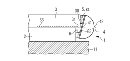
図1Aは、半導体レーザ1の例示的な実施形態の断面図を示し、図1Bは、平面図を示す。半導体レーザ1は、好ましくは、ヒートシンク11に実装され、ヒートシンク11と一緒に装置10を形成する。装置10は、通常環境空気12中に配置される。従って、装置10は、環境空気12に対して、それ以上封止されることも気密に密封されることもない。
1A shows a cross-sectional view of an exemplary embodiment of a semiconductor laser 1, and FIG. 1B shows a plan view. The semiconductor laser 1 is preferably mounted on the
半導体レーザ1は、キャリア2、特にいわゆるサブマウントを含む。キャリア2には、レーザ放射Lを発生するためのレーザダイオード3が配置される。レーザ放射は、例えば、青色光である。この目的で、レーザダイオード3は、活性領域33を有する。レーザ放射Lは、活性領域33の放射出口領域31において放出される。レーザダイオード3の好ましくは平面のファセット30は、活性領域33に対してほぼ垂直に配向している。
The semiconductor laser 1 includes a
ファセット30およびキャリア2の側面20には、接着剤5があり、これを用いて保護カバーが固定されている。保護カバーは、レンズ4として、好ましくは球面レンズとして設計され、ファセット30に面する光入射面41とファセット30から遠い光出射面42とを有する。
例えば、楕円形の放射出口領域31は、平面図において閉じた経路の中で周りをすべて接着剤5によって囲まれている。図1B参照。この場合、図1Bにおいて、例示を単純化するために、レンズ4は図示せず、保護カバー4は、すべての他の例示的な実施形態においても可能であると同じく、接着剤5の外側輪郭と一致して閉じることができる。
For example, the elliptical
従って、ファセット30において、保護カバー4により閉じ込められているキャビティ6が接着剤5によって画定される。キャビティ6は、排気されるかまたは保護ガスで満たされる。放射出口領域31に面するキャビティ6の側壁65は、断面図で見ると、キャビティ6が両凸に見えるように湾曲している。図1A参照。
Therefore, in the
上から見ると、放射出口領域31は、キャビティ6の中で中央に配置されてよい。図1B参照。接着剤5は、放射出口領域31の周りの異なる方向において異なる幅を有してよい。接着剤5は、好ましくは、薄く、それによって、ファセット30と光入射面41との間の平均距離は、好ましくは多くとも5μmである。任意選択として、光入射面41においてレーザ放射Lのための反射防止コーティング44が配置される。好ましくは、すべての他の例示的な実施形態にも同じことがあてはまる。
Seen from above, the
接着剤5および保護カバー4と一緒にキャビティ6を用いると、レーザダイオード3は、ファセットに近接した形態で封止される。この封止部は、レーザダイオード3の放射出口領域31を環境影響および汚染から保護する。従って、封止部は、局所的にレーザファセット30自体の領域および周囲の実装面に限定される。
When the
ファセット30の領域において、封止部は、キャビティ6を形成する。こうして形成されたキャビティ6は、環境影響に対して気密封止される。任意選択の保護ガスまたはガス混合物は、例えば、H2、He、N2、He/O2である。保護カバー4のアセンブリ時に、放射出口領域31は、接着剤5の間隙分だけ後退する。従って、保護カバー4および接着剤5から形成された封止部要素と放射出口領域31との間には、アセンブリ時にも半導体レーザ1の動作時にも物理的接触がない。
In the region of the
ファセットに近い封止部ならびにキャビティ6と保護カバー4との間の屈折率の飛躍に起因して、放出されたレーザ放射Lのレーザダイオード3の共振器への潜在的に後方への反射が起り、共振器の撹乱につながり得る。この相互作用を抑えるために、特に、そのような相互作用の代替的または追加的な防止可能策のための反射防止コーティング44が設けられる。以下の図2および図3も参照。
Due to the seal near the facet and the refractive index jump between the
キャビティ6を製造するために、例えば、ガラスでできている環構造体がレーザダイオード3およびキャリア2、または代りに、保護カバー4、特に、光入射面41に施用される。保護カバー4に接合するために、キャリア2およびレーザダイオード3は、好ましくは、必要な加工温度にされる。接合は、温度および、好ましくは、圧力の作用下で行われる。
To manufacture the
さらに、接着剤5を形成するガラススポンジを保護カバー4に施用することが可能である。この目的で、印刷法または分注法などのプロセスによってガラス粉体/バインダ混合物が保護カバー4に施用される。ネック形成とも呼ばれる下流の温度処理によって、バインダが除去され、ガラス粉体が焼結される。こうして調製した保護カバー4は、次に、温度および、任意選択として、圧力を用いてキャリア2およびレーザダイオード3の構造体に施用される。
Further, the glass sponge forming the adhesive 5 can be applied to the
あるいは、化学プロセスによって接着剤5のためのガラススポンジを製造してよい。この目的で、例えば、特に適応させたガラスの環構造体が保護カバー4に施用される。ガラスは、微視的規模での標的型の温度貯蔵によって、好ましくは2つ以上の相に偏析する。相の1つを湿式化学的に残るマトリックスから溶出させることができる。上記のように、こうして形成されたスポンジ状構造体をキャリア2および/またはレーザダイオード3に、あるいは保護カバー4にも実装することができる。接合は、しかるべく行われる。
Alternatively, a glass sponge for the adhesive 5 may be manufactured by a chemical process. For this purpose, for example, a specially adapted glass ring structure is applied to the
さらに、特に、保護カバー4ならびにキャリア2とレーザダイオード3との複合体に構造化メタライゼーションを施用することが可能である。接合のために金属接合要素が取り付けられる。接合要素は、例えば、ハンダ、金属スポンジまたは前もって製造された金属リングである。接合は、温度、および任意選択として、圧力の作用下で行われる。
Further, in particular, it is possible to apply structured metallization to the
放射出口領域31の領域中にマイクロキャビティ6を形成することによって、放射出口領域31と保護カバー4との間に機械的接触がない。チップに近いこの封止を用いると、いわゆるTOハウジングと比較して顕著な小型化を実現することができる。
By forming the
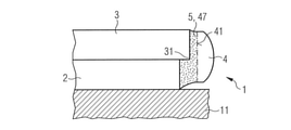
図2の例示的な実施形態において、保護カバー4は、レーザダイオード3に対して傾いた様相で施用される。光入射面41とファセット30との間の角度は、例えば、10°である。
In the exemplary embodiment of FIG. 2, the
光入射面41がこの場合は平面であり、光出射面42が半球である保護カバー4の直径は、例えば、0.2mm以上から0.8mm以下の間、特に0.4mm前後である。すべての他の例示的な実施形態に同じことがあてはまる。
In this case, the
それ以外の点において、図2の例示的な実施形態は、好ましくは、図1のものに対応する。 In other respects, the exemplary embodiment of FIG. 2 preferably corresponds to that of FIG.
反射したレーザ放射Lの影響を防ぐために、図3の例示的な実施形態の保護カバー4の光入射面41には粗面化部43がある。粗面化部43は、規則的な設計であっても不規則的な設計であってもよい。粗面化部43は、光入射面41全体にわたって延在してもよく、キャビティ6に割り当てられている保護カバー4の中心領域に限定されてもよい。粗面化部43の平均構造サイズは、好ましくは、少なくとも0.2μmおよび/または多くとも3μmである。
In order to prevent the influence of the reflected laser radiation L, the
レーザダイオード3の共振器に対する後方反射したレーザ放射Lによる影響を防ぐための可能な策も図4から図8と関連して説明される。
Possible measures to prevent the influence of the backward reflected laser emission L on the resonator of the
図4左側において、ファセット30に平行に後方反射したレーザ放射Rは、レーザダイオード3の共振器に届くことができることが示される。これは、レーザダイオード3に対する保護カバー4の傾いた配置によって防止される。図4右側参照。ファセット30と光入射面41との間の角度は、好ましくは5°以上から15°以下の間である。
On the left side of FIG. 4, it is shown that the laser emission R back-reflected parallel to the
図5は、図5の左側で起こる後方反射Rが、図5の右側では反射防止コーティング44によって防止されることを例示する。反射防止コーティング44は、例えば、図5に概略的にしか示さない、屈折率の高い層と屈折率の低い層との交互配列によって形成される。反射防止コーティング44は、光入射面41と光出射面42との両方に取り付けることができ、従って保護カバー4の実際の躯体を完全に囲むことができる。図1の実施形態においても同じことが可能である。
FIG. 5 illustrates that the back-reflection R that occurs on the left side of FIG. 5 is prevented by the
図4および図5において同じく、接着剤5は、図1から図3の場合と異なり、放射出口領域31を完全に覆う。従って、キャビティが形成されない。接着剤5は、従って、好ましくは、レーザ放射Lに対して、特にガラスから、またはガラス混合物から透過性であるように形成される。接着剤5は、従って、すべての他の例示的な実施形態において可能であると同様に、無機成分である。
Similarly in FIGS. 4 and 5, the adhesive 5 completely covers the
図6は、粗面化部43が図3と同様に光入射面41に存在することを示す。粗面化部43は、図3および図6の図示から逸脱して、光入射面41を部分的にのみ覆うこともできる。図3を参照し、図1も参照する説明は、キャビティの省略を除いて、図6に対応してあてはまる。
FIG. 6 shows that the roughened
すべての他の例示的な実施形態におけると同じように、保護カバー4が、断面図に見られるように、光入射面41と光出射面42との間の側面がまっすぐであることが可能である。側面は、例えば、円筒形の側面を表す。
As in all other exemplary embodiments, the
図7において、光入射面41が、撹乱する後方反射を防ぐように特に設計されることが示される。この目的で、保護カバー4の形は、断面図で見ると、ほぼ両凸である。光入射面41の最大のふくらみの領域は、活性領域33に対して、従って放射出口領域31に対してずらされ、それによって、光入射面41は、放射出口領域31においてファセット30と平行に配向しない。
In FIG. 7, it is shown that the
図8の例示的な実施形態において、接着剤5は、屈折率適合層47として設計される。従って、接着剤5と保護カバー4との間に一点鎖線によって象徴される屈折率の飛躍がないか、またはあまりない。それ以外の点は、ここまでの例示的な実施形態に関する記載が対応してあてはまる。
In the exemplary embodiment of FIG. 8, the adhesive 5 is designed as a refractive index compatible layer 47. Therefore, there is little or no jump in refractive index symbolized by the alternate long and short dash line between the adhesive 5 and the
ここまでの図において、各々の場合に、レーザダイオード3の共振器への後方反射を防ぐための手段は、1つしか描かれていない。これらの手段を組合せても行い得る。例えば、粗面化部43または湾曲型光入射面41を光入射面41の傾斜配置と組合せてよい。各々の場合に反射防止コーティング44も存在し得る。例示的な実施形態、特に図5から図7のものにおいて、屈折率適合層47も用いてよい。
In the figures so far, in each case, only one means for preventing the back reflection of the
特に、図8の設計において、接着剤5および保護カバー4が同じまたは非常に類似した材料であることも可能である。しかし、接着剤5の加工温度は、好ましくは、保護カバー4のものより低い。
In particular, in the design of FIG. 8, it is possible that the adhesive 5 and the
ファセットに近い封止の場合に保護カバー4とレーザダイオード3の共振器との間の光相互作用を低下させるかまたはなくすことによって、設計における追加の自由度が実現される。特に、小型化設計が維持される。
Additional degrees of freedom in design are provided by reducing or eliminating the optical interaction between the
図9の例示的な実施形態において、すべての他の例示的な実施形態においても当てはめてもよいように、レーザダイオード3は、ボンディングワイヤ13を介してヒートシンク11に接続されることが示される。すべての他の例示的な実施形態においても可能であるように、接着剤5は、ヒートシンク11まで届くことができ、この場合、キャリア2から距離をおいて延在してもよく、あるいは、キャリア2がレーザダイオード3に集積化される。
In the exemplary embodiment of FIG. 9, the
レーザ放射Lが放出される、環境空気12にアクセス可能な境界面は、ファセットに近い所で用いられる保護カバー4によって顕著に増加する。その結果、光ピンセットなどの効果は、低下し、界面、すなわち、光出射面42におけるレーザ放射Lの強度は、低下する。
The accessible interface of the
それ以外の点は、図1から図8に関する記載が対応して図9にあてはまる。 Other than that, the description with respect to FIGS. 1 to 8 corresponds to FIG. 9.
図10において、光出射面42は、好ましくは、光触媒コーティング45および/または接着防止コーティング46によって完全に覆われることが示される。光触媒コーティング45は、例えば、薄い白金層または二酸化チタン層である。そのようなコーティング45を用いると、保護カバー4の光出射面42上の汚染物質の堆積と潜在的な堆積物の分解との熱力学的平衡を、半導体レーザ1の動作期間にわたって堆積物の蓄積が確実に減るように移行させることができる。
In FIG. 10, it is shown that the
接着防止コーティング46を施用することによって、光出射面42において不純物の蓄積は起こらないか、またはあまり起こらず、不純物の焼き付きも起こらないということが可能である。接着防止コーティング46は、好ましくは、レーザ放射Lに対して透明である。接着防止コーティング46は、例えば、ポリテトラフルオロエチレンなどのフルオロポリマーによって形成される。接着防止コーティング46のための他の可能な材料は、ペリレンHTなどのペリレン誘導体またはチオール-R-D-Hなどの硫黄化合物またはカーボンナノチューブの層状構造体である。
By applying the anti-adhesion coating 46, it is possible that the accumulation of impurities on the
例えば、図9または10の半導体部品は、好ましくは、接着法によって保護カバー4を適当な接着剤5で結合し、任意選択として、後続の加熱プロセスおよび/またはベーキングプロセスを用いて製造される。純度が非常に高く炭化水素含有率が低いシリコーン系接着剤が保護カバー4を接着させるために適している。そのような接着剤5の中に存在するあらゆる揮発性添加物は、任意選択として、特に180℃から300℃の範囲の温度貯蔵によって放出される。残存炭化水素は、今度は、任意選択として、レーザ放射Lの出力および環境温度に関して定められる条件に基づくベーキングプロセスによって追い出される。
For example, the semiconductor component of FIG. 9 or 10 is preferably manufactured by bonding the
あるいは、ガラスを接着剤5として用いて保護カバー4を接着することが可能である。この場合、好ましくは、中融点ガラスが用いられる。ガラスは、接合される2つの表面の一方に、または両方の表面に施用される。ガラスは、好ましくは、300℃から450℃の温度範囲において液体分散によって施用される。そのような分注法の後、保護カバー4は、例えば、ピックアンドプレイスとも呼ばれるグリッピングプロセスを用いて、レーザダイオード3のファセット30に実装される。
Alternatively, the
図11は、オプトエレクトロニクス半導体部品1、図11によって製造される半導体レーザ1のための製造方法を示す。この場合、図1から図10に関連して用いた接着剤5をまったくなしですませ、それでも放射出口領域31の気密封止を確保することが可能である。
FIG. 11 shows a manufacturing method for the optoelectronic semiconductor component 1 and the semiconductor laser 1 manufactured by FIG. In this case, the adhesive 5 used in connection with FIGS. 1 to 10 is completely eliminated, and it is still possible to secure the airtight seal of the
この目的で、図11Aを参照し、原料48、好ましくは、ファセット30および/またはキャリア2の側面20にガラスが、特に液体状態で分注法を用いて、施用される。あるいは、スリップとも呼ばれるガラス粉体が施用され、ガラス粉体は、好ましくは、バインダ溶液で施用される。施用は、分注法、噴霧法、印刷法または噴射法によって行ってよく、好ましくは、続いて脱バインダおよび締固めのために温度貯蔵工程を行う。
For this purpose, reference to FIG. 11A, glass is applied to the
あるいは、ガラスビーズが入れられ、続いて、レーザ融解プロセスとも呼ばれる、レーザ溶接プロセスと同様な取り付けのための標的型局所温度処理が行われる。レーザ融解の場合、ガラスの滴の形は、ビームプロファイル中のエネルギー密度分布の標的型調整、例えば、正規プロファイルまたはいわゆるトップハットプロファイルによる局所融解の影響を受ける可能性がある。 Alternatively, glass beads are placed and followed by a targeted local temperature treatment for attachment similar to a laser welding process, also known as a laser melting process. In the case of laser melting, the shape of the glass droplets can be affected by targeted adjustment of the energy density distribution in the beam profile, for example local melting by a normal profile or a so-called top hat profile.
適当なガラス組成物の例は、特に、光学ガラス、特にガラス転移点が低く400℃を超えないガラス、またはガラス転移点が非常に低く300℃未満のガラスの群からである。そのようなガラスは、好ましくは、酸化テルルTe2O5、三酸化ホウ素B2O3、シリカSiO2、または酸化ビスマスBi2O3のようなガラス形成体に基づく。適当なガラス組成物は、好ましくは、ネットワーク中断材、例えばZnOおよび/またはCaOの割合が高い。そのようなガラス組成物を安定させるため、または結晶化する傾向を低く保つために、酸化アルミニウムAl2O3を任意選択として加えてよい。 Examples of suitable glass compositions are, in particular, from the group of optical glasses, in particular glass having a low glass transition point not exceeding 400 ° C., or glass having a very low glass transition point of less than 300 ° C. Such glasses are preferably based on glass forms such as tellurium oxide Te 2 O 5 , boron trioxide B 2 O 3 , silica SiO 2 , or bismuth oxide Bi 2 O 3 . Suitable glass compositions preferably have a high proportion of network interrupting material, such as ZnO and / or CaO. Aluminum oxide Al 2 O 3 may be added as an option to stabilize such glass compositions or to keep their tendency to crystallize low.
そのようなガラスは、特に図1から図3の接着剤5、ならびに、例えば、図4から図8の接着剤5のためにも用いることができる。
Such glass can also be used specifically for the adhesive 5 of FIGS. 1 to 3, and also, for example, the
あるいは、または加えて、接着剤5を施用したレーザダイオード3および/またはキャリア2の加熱は、特に、ガラスの温度がエンボス法による整形のために十分低い粘度になるまで行われる。好ましくは、図11Bを参照し、加熱することができるホットスタンプ用ツール49を用いるエンボス法プロセスは、好ましくは、104dPa・sから108dPa・sの範囲、好ましくは104dPa・sから105dPa・sの範囲の接着剤5の粘度で行われる。
Alternatively, or in addition, heating of the
スタンプ用ツール49は、例えば、白金、金、白金-金合金またはグラファイトでできている。さらに、硬質金属のツール49が適している。これらのものの例は、特にコバルトのマトリックス中の炭化タングステンまたは炭化チタンである。
The
ホットスタンプ用ツール49は、接着剤5の接着を防ぐコーティングを有し得る。そのようなコーティングは、例えば、TiN、AlNおよび/またはTiAlNである。好ましくは、低い表面粗さ、例えば、粗さRaが多くとも100nmであるエンボス用ツール49が用いられる。この目的で、特に、表面被覆されるか、または表面締固めされたグラファイトが適している。
The
施用された保護カバー4は、標的型光線整形のために用いることができる。あるいは、保護カバー4は、屈折光学部品として、回折光学部品として、または両方の組合せとして設計することもできる。光出力を増すための構造として保護カバー4の光学的に有効な構造を設計することができる。図12も参照。
The applied
図11Cに仕上げられた半導体部品1が例示される。この場合、ファセット30全体およびキャリア2の側面20全体が保護カバー4によって覆われることが可能である。
The semiconductor component 1 finished in FIG. 11C is exemplified. In this case, the
図12の方法において、オプトエレクトロニクス半導体チップ3は、LEDチップであり、好ましくは、集積化されたキャリア2、または代りに図示していない別々のキャリアを有する。任意選択として、半導体チップ3は、接続手段14、例えば接着点またはハンダ点を介して、キャリア11に取り付けられる。図12Aを参照すると、原料48が保護カバー4に施用される。
In the method of FIG. 12, the
続いて、図12Bを参照し、エンボス用ツール49を用いてエンボス法が行われ、それによって、図12Cに例示されるように、例えば、光出力を向上させる保護カバー4が得られる。このように光出射面42において粗面化部43を含む保護カバー4が形成される。この目的で、保護カバー4の屈折率は、例えば、屈折率差が多くとも0.3である、半導体チップ3と同様であってよく、その結果、高屈折率原料48を保護カバー4のために用いることができる。
Subsequently, with reference to FIG. 12B, an embossing method is performed using the
図13の例示的な実施形態において、保護カバー4は、レンズとしてではなく面平行な円板として設計される。ファセット30は、部分的にしか接着剤5によって覆われず、側面20と同一平面で終端する。すべての他の例示的な実施形態において同じことが可能である。
In the exemplary embodiment of FIG. 13, the
図14によると、例えば、面平行セラミックプレートの形のルミネセンス要素7が保護カバー4に取り付けられる。接続手段14、例えば、特に、厚さが0.2μmから3μmの間である薄いシリコーン接着剤の層だけが、例えば、面平行保護カバー4とルミネセンス要素7との間に配置される。
According to FIG. 14, for example, a
波長変換のための少なくとも1種類の蛍光体は、動作時に発生するレーザ放射Lがルミネセンス要素7に衝突するルミネセンス要素7の領域に限定することができる。任意選択として、レーザダイオード3に面するルミネセンス要素7の入射面72に、レーザ放射Lについては透明であるが、ルミネセンス要素7の中で発生する放射を反射する二色性コーティング73が配置される。
The at least one type of phosphor for wavelength conversion can be limited to the region of the
さらに、キャリア2が側面30より上に突き出ることが可能である。従って、保護カバー4は、キャリアとは反対側を向いてよく、キャリア2に対して斜めになってよい。すべての他の例示的な実施形態において同じことをあてはめてよい。
Further, the
同様に、図15の例示的な実施形態において、ルミネセンス要素7が存在する。この場合、ルミネセンス要素7は、直接、特に、光出射面42の表面全体の上に、好ましくは、一定の変化しない厚さで施用される。
Similarly, in the exemplary embodiment of FIG. 15, the
そのようなルミネセンス要素7も、図14および図15において説明したように、すべての他の例示的な実施形態において、好ましくは二色性コーティング73と一緒に存在してよい。
Such a
図13から図15の構成において、レーザダイオード3の共振器への後方反射を防ぐための手段も、図1から図8における構成と同じように、個々に、または互いに組合されて取られてよい。
In the configurations of FIGS. 13 to 15, the means for preventing the back reflection of the
特に断らない限り、図に示す構成要素は、それぞれの場合に指定された順番で直接、互いの後に続く。図において接触していない層は、好ましくは、互いに離間している。線が互いに平行に描かれている場合、対応する表面は、好ましくは、同様に互いに平行に配向している。同様に、特に断らない限り、図示された構成要素の互いに対する相対的な位置は、図において正しく再現される。 Unless otherwise noted, the components shown in the figure follow each other directly in the order specified in each case. The layers that are not in contact in the figure are preferably separated from each other. When the lines are drawn parallel to each other, the corresponding surfaces are preferably oriented parallel to each other as well. Similarly, unless otherwise noted, the relative positions of the illustrated components relative to each other are correctly reproduced in the figure.
本明細書に記載される発明は、例示的な実施形態を参照する明細書によって限定されない。本発明は、詳しくは、請求項にある特徴のあらゆる組合せを含む、各々の新規な特徴ならびに特徴のあらゆる組合せを、たとえこの特徴または組合せそれ自体は、請求項または実施形態に明示的に挙げられていないとしても、含む。 The inventions described herein are not limited by the specification with reference to exemplary embodiments. The present invention specifically mentions any novel feature as well as any combination of features, including any combination of the features in the claims, even the features or combinations themselves are expressly mentioned in the claims or embodiments. Includes, if not.
本特許出願は、独国特許出願第10 2017 123 798.4号の優先権を主張し、ここでその開示内容は参照により援用される。 This patent application claims the priority of German Patent Application No. 10 2017 123 798.4, the disclosure of which is incorporated herein by reference.
1 半導体レーザおよびオプトエレクトロニクス半導体部品
2 キャリア
20 キャリア側面
3 レーザダイオードおよびオプトエレクトロニクス半導体チップ
30 ファセット
31 放射出口領域
33 活性領域
4 保護カバー/レンズ
41 光入射面
42 光出射面
43 粗面化部
44 反射防止コーティング
45 光触媒コーティング
46 接着防止コーティング
47 屈折率適合層
48 レンズ原料
49 ホットスタンプ用ツール
5 接着剤
6 キャビティ
65 キャビティの側壁
7 ルミネセンス要素
72 入射面
73 二色性コーティング
10 装置
11 ヒートシンク
12 環境空気
13 ボンディングワイヤ
14 接続手段
L レーザ放射
R ファセットと光入射面との間のレンズ角度で反射されるレーザ放射
1 Semiconductor laser and
Claims (16)
前記キャリア(2)に実装され、レーザ放射(L)を発生するための活性領域(33)を有し、放射出口領域(31)を有するファセット(30)を有する端面発光型のレーザダイオード(3)と、
保護カバー(4)と、
前記保護カバー(4)が、前記ファセット(30)におよび前記キャリア(2)の側面(20)に固定される接着剤(5)と、
を含む半導体レーザ(1)であって、
前記保護カバー(4)の光入射面(41)と前記ファセット(30)との間の平均距離は、多くとも15μmであり、
前記光入射面(41)は、平らであり、
前記ファセット(30)上の前記活性領域(33)の領域にキャビティ(6)が形成され、前記キャビティ(6)は、前記ファセット(30)の平面図で見ると、前記接着剤(5)によって周りをすべて囲まれ、且つ、前記保護カバー(4)によって限定されており、それによって、前記レーザ放射(L)が前記レーザダイオード(3)を離れる前記放射出口領域(31)は、接着剤(5)を含まず、
前記半導体レーザ(1)は、前記保護カバー(4)および前記接着剤(5)によって気密に密封されて通常雰囲気中で追加の気密封止なしで動作するように構成される、
半導体レーザ(1)。 Carrier (2) and
An end face emitting laser diode (3) mounted on the carrier (2), having an active region (33) for generating laser radiation (L), and having a facet (30) having a radiation outlet region (31) . )When,
Protective cover (4) and
With the adhesive (5), the protective cover (4) is fixed to the facet (30) and to the side surface (20) of the carrier (2).
A semiconductor laser (1) containing
The average distance between the light incident surface (41) of the protective cover (4) and the facet (30) is at most 15 μm.
The light incident surface (41) is flat and is flat.
A cavity (6) is formed in the region of the active region (33) on the facet (30), and the cavity (6) is formed by the adhesive (5) when viewed in a plan view of the facet (30). All around and limited by the protective cover (4), the radiation outlet region (31) from which the laser emission (L) leaves the laser diode (3) is an adhesive (31). 5) is not included
The semiconductor laser (1) is hermetically sealed by the protective cover (4) and the adhesive (5) and configured to operate in a normal atmosphere without additional hermetic sealing.
Semiconductor laser (1).
請求項1に記載の半導体レーザ(1)。 The protective cover (4) is a prism for beam deflection.
The semiconductor laser (1) according to claim 1 .
請求項1に記載の半導体レーザ(1)。 The protective cover (4) is a lens for collimation of the laser emission (L), and the minimum distance from the facet (30) is 0.1 μm .
The semiconductor laser (1) according to claim 1.
前記キャビティ(6)の平均直径は、前記ファセット(30)の平面図で見ると、3μm以上から100μm以下の間であり、前記キャビティ(6)の厚さは、0.5μm以上から20μm以下の間であり、
前記ファセット(30)の平面図で見ると、前記キャビティ(6)の周りの前記接着剤(5)の幅は、前記キャビティ(6)の前記平均直径の少なくとも150%であり、少なくとも30μmでもある、
請求項1に記載の半導体レーザ(1)。 The cavity (6) is exhausted or filled with at least one protective gas.
The average diameter of the cavity (6) is between 3 μm and more and 100 μm or less when viewed from the plan view of the facet (30), and the thickness of the cavity (6) is 0.5 μm or more and 20 μm or less. Between
Looking at the plan view of the facet (30), the width of the adhesive (5) around the cavity (6) is at least 150% of the average diameter of the cavity (6) and is also at least 30 μm. ,
The semiconductor laser (1) according to claim 1 .
前記レーザ放射(L)は、前記接着剤(5)から前記光入射面(41)の方へ距離をおいて通る、
請求項1から4のいずれか一項に記載の半導体レーザ(1)。 The cavity (6) is toward the adhesive (5) so that the cavity (6) has a biconvex shape in the radiation outlet region (31) when viewed in cross section perpendicular to the facet (30). Has a curved side wall (65) to
The laser emission (L) passes from the adhesive (5) toward the light incident surface (41) at a distance.
The semiconductor laser (1) according to any one of claims 1 to 4 .
前記レーザ放射(L)の最大強度の波長は、365nm以上から530nm以下の間である、
請求項1から5のいずれか一項に記載の半導体レーザ(1)。 The protective cover (4) has or comprises at least one of the following materials: sapphire, SiC, or consists of at least one of these materials.
The wavelength of the maximum intensity of the laser emission (L) is between 365 nm and more and 530 nm or less.
The semiconductor laser (1) according to any one of claims 1 to 5 .
前記光入射面(41)と前記ファセット(30)との間の角度(α)は、5°以上から25°以下の間である、
請求項1から8のいずれか一項に記載の半導体レーザ(1)。 The planar light incident surface (41) is such that the laser radiation (L) reflected by the light incident surface (41) is kept away from the radiation outlet region (31) and / or the laser diode (3). ) Is obliquely oriented with respect to the facet (30) so that it remains undisturbed by the reflected laser radiation (L).
The angle (α) between the light incident surface (41) and the facet (30) is between 5 ° and more and 25 ° or less.
The semiconductor laser (1) according to any one of claims 1 to 8 .
請求項1から8のいずれか一項に記載の半導体レーザ(1)。 At least the light incident surface (41) is such that the light incident surface (41) has a reflectivity of at most 0.5% due to the laser emission (L) and / or the laser diode (3). ) Is provided with an antireflection coating (44) for the laser emission (L) so that it remains undisturbed by the reflected laser emission (L).
The semiconductor laser (1) according to any one of claims 1 to 8 .
前記光触媒コーティング(45)は、前記レーザ放射(L)を利用して前記光出射面(42)上の堆積物を除去および/または分解するように構成される、
請求項1から10のいずれか一項に記載の半導体レーザ(1)。 At least one light emitting surface (42) of the protective cover (4) opposite to the facet (30) is provided with a photocatalytic coating (45).
The photocatalytic coating (45) is configured to utilize the laser emission (L) to remove and / or decompose deposits on the light emitting surface (42).
The semiconductor laser (1) according to any one of claims 1 to 10 .
前記接着防止コーティング(46)は、前記保護カバー(4)の外側における堆積物を防ぐように構成される、
請求項1から10のいずれか一項に記載の半導体レーザ(1)。 At least one light emitting surface (42) of the protective cover (4) opposite to the facet is provided with an anti-adhesive coating (46).
The anti-adhesive coating (46) is configured to prevent deposits on the outside of the protective cover (4).
The semiconductor laser (1) according to any one of claims 1 to 10 .
前記ファセット(30)は、前記レーザ放射(L)の通る方向に沿って、前記キャリア(2)を超えて突き出る、
請求項1から12のいずれか一項に記載の半導体レーザ(1)。 The active region (33) is arranged on the side of the laser diode (3) facing the carrier (2).
The facet (30) protrudes beyond the carrier (2) along the direction through which the laser radiation (L) passes.
The semiconductor laser (1) according to any one of claims 1 to 12 .
前記ルミネセンス要素(7)は、前記光出射面(42)に直接配置される、
請求項11または12に記載の半導体レーザ(1)。 Further comprising a luminescence element (7) for partially converting the laser emission (L) such that the semiconductor laser (1) emits white mixed light during operation.
The luminescence element (7) is placed directly on the light emitting surface (42).
The semiconductor laser (1) according to claim 11 or 12 .
放射(L)を発生するための活性領域(33)を有し、放射出口領域(31)を有するオプトエレクトロニクス半導体チップ(3)を提供することと、
続いて、前記放射出口領域(31)において直接、保護カバー(4)を製造することと、
を含み、
前記保護カバー(4)は、ガラス製であり、ホットスタンプ法を用いて製造され、
前記オプトエレクトロニクス半導体部品(1)は、前記保護カバー(4)によって気密に密封されて通常雰囲気中で追加の気密封止なしで動作するように構成される、
方法。 Optoelectronics A method for manufacturing semiconductor components (1).
To provide an optoelectronic semiconductor chip (3) having an active region (33) for generating radiation (L) and having a radiation outlet region (31).
Subsequently, the protective cover (4) is directly manufactured in the radiation outlet region (31), and
Including
The protective cover (4) is made of glass and is manufactured by a hot stamping method.
The optoelectronic semiconductor component (1) is hermetically sealed by the protective cover (4) and configured to operate in a normal atmosphere without additional hermetic sealing.
Method.
前記保護カバー(4)は、収束レンズであり、前記ファセット(30)に平行に通るキャリア(2)の側面(20)に多くとも15°の公差で直接触れる、
請求項15に記載の方法。 The optoelectronics semiconductor chip (3) is a laser diode having a facet (30) including the radiation outlet region (31).
The protective cover (4) is a condensing lens and directly touches the side surface (20) of the carrier (2) parallel to the facet (30) with a tolerance of at most 15 °.
The method according to claim 15 .
Priority Applications (1)
| Application Number | Priority Date | Filing Date | Title |
|---|---|---|---|
| JP2022002276A JP7256302B2 (en) | 2017-10-12 | 2022-01-11 | semiconductor laser |
Applications Claiming Priority (3)
| Application Number | Priority Date | Filing Date | Title |
|---|---|---|---|
| DE102017123798.4A DE102017123798B4 (en) | 2017-10-12 | 2017-10-12 | Semiconductor lasers and manufacturing processes for optoelectronic semiconductor components |
| DE102017123798.4 | 2017-10-12 | ||
| PCT/EP2018/077313 WO2019072759A1 (en) | 2017-10-12 | 2018-10-08 | Semiconductor laser and method of production for optoelectronic semiconductor parts |
Related Child Applications (1)
| Application Number | Title | Priority Date | Filing Date |
|---|---|---|---|
| JP2022002276A Division JP7256302B2 (en) | 2017-10-12 | 2022-01-11 | semiconductor laser |
Publications (2)
| Publication Number | Publication Date |
|---|---|
| JP2020537337A JP2020537337A (en) | 2020-12-17 |
| JP7008808B2 true JP7008808B2 (en) | 2022-01-25 |
Family
ID=63832414
Family Applications (3)
| Application Number | Title | Priority Date | Filing Date |
|---|---|---|---|
| JP2020519069A Active JP7008808B2 (en) | 2017-10-12 | 2018-10-08 | Manufacturing methods for semiconductor lasers and optoelectronic semiconductor components |
| JP2022002276A Active JP7256302B2 (en) | 2017-10-12 | 2022-01-11 | semiconductor laser |
| JP2023055382A Active JP7523619B2 (en) | 2017-10-12 | 2023-03-30 | Semiconductor laser |
Family Applications After (2)
| Application Number | Title | Priority Date | Filing Date |
|---|---|---|---|
| JP2022002276A Active JP7256302B2 (en) | 2017-10-12 | 2022-01-11 | semiconductor laser |
| JP2023055382A Active JP7523619B2 (en) | 2017-10-12 | 2023-03-30 | Semiconductor laser |
Country Status (6)
| Country | Link |
|---|---|
| US (3) | US11735887B2 (en) |
| JP (3) | JP7008808B2 (en) |
| KR (1) | KR102425947B1 (en) |
| CN (1) | CN111542976A (en) |
| DE (1) | DE102017123798B4 (en) |
| WO (1) | WO2019072759A1 (en) |
Families Citing this family (9)
| Publication number | Priority date | Publication date | Assignee | Title |
|---|---|---|---|---|
| DE102018113711A1 (en) | 2018-06-08 | 2019-12-12 | Osram Opto Semiconductors Gmbh | APPARATUS AND HEADLIGHTS |
| DE102018117518A1 (en) | 2018-07-19 | 2020-01-23 | Osram Opto Semiconductors Gmbh | Semiconductor laser |
| JP7476895B2 (en) * | 2019-07-09 | 2024-05-01 | ソニーグループ株式会社 | Wavelength conversion element |
| DE102020118159A1 (en) | 2020-07-09 | 2022-01-13 | OSRAM Opto Semiconductors Gesellschaft mit beschränkter Haftung | LASER DEVICE |
| KR102344931B1 (en) * | 2020-08-14 | 2021-12-31 | 주식회사 레신저스 | Polymer rod for shaping emitting light to synmetrical light |
| DE102020127450A1 (en) * | 2020-10-19 | 2022-04-21 | OSRAM Opto Semiconductors Gesellschaft mit beschränkter Haftung | OPTOELECTRONIC DEVICE AND METHOD FOR MANUFACTURING OPTOELECTRONIC DEVICE |
| DE102022103260A1 (en) | 2022-02-11 | 2023-08-17 | Ams-Osram International Gmbh | LASER COMPONENT |
| WO2024074254A1 (en) | 2022-10-05 | 2024-04-11 | Ams-Osram International Gmbh | Optoelectronic light source and data glasses |
| CN116107146A (en) * | 2023-03-13 | 2023-05-12 | 青岛海信激光显示股份有限公司 | Light source assembly and projection equipment |
Citations (13)
| Publication number | Priority date | Publication date | Assignee | Title |
|---|---|---|---|---|
| US20030007257A1 (en) | 2001-07-06 | 2003-01-09 | Bell Bernard W. | Facial contact lens system for laser diode |
| JP2004103792A (en) | 2002-09-09 | 2004-04-02 | Ricoh Co Ltd | Compound optical device and method of manufacturing the same |
| JP2007157961A (en) | 2005-12-05 | 2007-06-21 | Sony Corp | Semiconductor laser device and manufacturing method thereof |
| JP2008146750A (en) | 2006-12-11 | 2008-06-26 | Matsushita Electric Ind Co Ltd | Optical member sticking method for semiconductor device |
| JP2009099664A (en) | 2007-10-15 | 2009-05-07 | Nichia Corp | Light-emitting device |
| JP2009260118A (en) | 2008-04-18 | 2009-11-05 | Konica Minolta Opto Inc | Optical module |
| JP2011003889A (en) | 2009-05-21 | 2011-01-06 | Nichia Corp | Semiconductor laser device and method for manufacturing the same |
| DE102009040834A1 (en) | 2009-09-09 | 2011-05-19 | Jenoptik Laserdiode Gmbh | Diode laser component, has sealing device provided for sealing free space with respect to surrounding, and sealing ring sections accomplishing sealing of partial contributions between optics unit and contact bodies, respectively |
| JP2011119699A (en) | 2009-11-05 | 2011-06-16 | Nichia Corp | Semiconductor laser device and method of manufacturing the same |
| WO2014192939A1 (en) | 2013-05-30 | 2014-12-04 | 古河電気工業株式会社 | Optical module |
| JP2014232790A (en) | 2013-05-29 | 2014-12-11 | パナソニック株式会社 | Semiconductor laser device and manufacturing method thereof |
| US20150244148A1 (en) | 2012-09-27 | 2015-08-27 | Osram Opto Semiconductors Gmbh | Optoelectronic Component |
| JP2016225448A (en) | 2015-05-29 | 2016-12-28 | セイコーエプソン株式会社 | Light source device and projector |
Family Cites Families (87)
| Publication number | Priority date | Publication date | Assignee | Title |
|---|---|---|---|---|
| US4001719A (en) * | 1975-08-13 | 1977-01-04 | Bell Telephone Laboratories, Incorporated | Fabrication of a self-aligned mirror on a solid-state laser for controlling filamentation |
| JPS5923479B2 (en) * | 1978-06-22 | 1984-06-02 | 三菱電機株式会社 | Method for manufacturing semiconductor light emitting device |
| JPS5910597B2 (en) * | 1979-07-09 | 1984-03-09 | シャープ株式会社 | Semiconductor laser array and its manufacturing method |
| GB8728342D0 (en) * | 1987-12-03 | 1988-01-06 | Bt & D Technologies Ltd | Light sources |
| JPH0744313B2 (en) * | 1989-02-24 | 1995-05-15 | 日本電信電話株式会社 | Semiconductor laser device |
| JPH02262389A (en) * | 1989-03-31 | 1990-10-25 | Toshiba Corp | Semiconductor laser device and its manufacture |
| JPH0334387A (en) * | 1989-06-29 | 1991-02-14 | Nec Corp | Semiconductor laser device |
| JPH043989A (en) * | 1990-04-20 | 1992-01-08 | Omron Corp | Light-emitting device |
| US5226052A (en) * | 1990-05-08 | 1993-07-06 | Rohm, Ltd. | Laser diode system for cutting off the environment from the laser diode |
| US5081639A (en) * | 1990-10-01 | 1992-01-14 | The United States Of America As Represented By The United States Department Of Energy | Laser diode assembly including a cylindrical lens |
| EP0504330A4 (en) * | 1990-10-01 | 1993-10-13 | United States Department Of Energy | Laser diode assembly including a cylindrical lens |
| US5206878A (en) * | 1991-10-11 | 1993-04-27 | At&T Bell Laboratories | Wide strip diode laser employing a lens |
| JPH05134150A (en) * | 1991-11-11 | 1993-05-28 | Fujitsu Ltd | Manufacture of condenser lens for emission element |
| JP3197034B2 (en) * | 1991-12-04 | 2001-08-13 | シャープ株式会社 | Semiconductor laser device |
| US5274732A (en) * | 1992-01-06 | 1993-12-28 | Eastman Kodak Company | Mount for linear lens array |
| EP0562754A1 (en) * | 1992-03-26 | 1993-09-29 | Hewlett-Packard Company | Optical system for laser devices |
| US5465265A (en) * | 1992-06-24 | 1995-11-07 | Fuji Xerox Co., Ltd. | Multi-beam laser light source and multi-beam semiconductor laser array |
| JP3381073B2 (en) * | 1992-09-28 | 2003-02-24 | ソニー株式会社 | Semiconductor laser device and method of manufacturing the same |
| US5414293A (en) * | 1992-10-14 | 1995-05-09 | International Business Machines Corporation | Encapsulated light emitting diodes |
| DE69312667T2 (en) * | 1993-01-04 | 1998-02-12 | Philips Electronics Nv | Beam-shaping optical element, radiation source and scanning unit with this element |
| US5615052A (en) * | 1993-04-16 | 1997-03-25 | Bruce W. McCaul | Laser diode/lens assembly |
| JPH07115244A (en) * | 1993-10-19 | 1995-05-02 | Toyota Motor Corp | Semiconductor laser and its fabrication |
| US5420722A (en) * | 1993-10-25 | 1995-05-30 | Creo Products Inc. | Self-registering microlens for laser diodes |
| US5544184A (en) * | 1994-06-10 | 1996-08-06 | Sdl, Inc. | Semiconductor illumination system with expansion matched components |
| JPH08191172A (en) * | 1995-01-12 | 1996-07-23 | Ricoh Opt Ind Co Ltd | Light-emitting element having minute optical element and minute optical element |
| US5636059A (en) * | 1995-02-08 | 1997-06-03 | Blue Sky Research, Incorporated | Cylindrical microlens external cavity for laser diode frequency control |
| US5802086A (en) * | 1996-01-29 | 1998-09-01 | Laser Power Corporation | Single cavity solid state laser with intracavity optical frequency mixing |
| US5757830A (en) * | 1996-02-07 | 1998-05-26 | Massachusetts Institute Of Technology | Compact micro-optical edge-emitting semiconductor laser assembly |
| DE19640423C1 (en) | 1996-09-30 | 1998-03-26 | Siemens Ag | Optoelectronic module for bidirectional optical data transmission |
| DE19706276B4 (en) * | 1997-02-18 | 2011-01-13 | Siemens Ag | A semiconductor laser device and method of manufacturing a semiconductor laser device |
| KR100413791B1 (en) * | 1997-05-30 | 2004-02-14 | 삼성전자주식회사 | Blue semiconductor laser device having curve reflector |
| US6314117B1 (en) * | 1998-12-16 | 2001-11-06 | Quan Photonics, Inc | Laser diode package |
| US6636538B1 (en) * | 1999-03-29 | 2003-10-21 | Cutting Edge Optronics, Inc. | Laser diode packaging |
| DE19963805B4 (en) | 1999-12-30 | 2005-01-27 | Osram Opto Semiconductors Gmbh | White light source based on non-linear optical processes |
| JP2001242357A (en) * | 2000-02-28 | 2001-09-07 | Alps Electric Co Ltd | Optical semiconductor device |
| DE10042904C2 (en) * | 2000-08-31 | 2003-03-13 | Infineon Technologies Ag | Semiconductor laser chip with integrated beam former and method for producing a semiconductor laser chip with integrated beam former |
| JP2003059087A (en) | 2001-08-15 | 2003-02-28 | Sony Corp | Optical element, semiconductor laser, optical detector, optical head and optical disk player |
| JP3975066B2 (en) * | 2001-10-12 | 2007-09-12 | 株式会社トプコン | Laser oscillator |
| JP2003207601A (en) | 2002-01-15 | 2003-07-25 | Ricoh Co Ltd | Objective lens, optical pickup module and optical disk device |
| WO2003077389A1 (en) | 2002-03-08 | 2003-09-18 | Sharp Kabushiki Kaisha | Light source apparatus and optical communication module comprising it |
| US20030219211A1 (en) * | 2002-05-22 | 2003-11-27 | Yu-Sik Kim | Method for aligning optical axis of an optical module |
| JP2004072004A (en) * | 2002-08-09 | 2004-03-04 | Keiji Tanaka | Light emitting element having micro-lens, and forming method thereof |
| US7146106B2 (en) * | 2002-08-23 | 2006-12-05 | Amkor Technology, Inc. | Optic semiconductor module and manufacturing method |
| US7192199B2 (en) * | 2003-12-26 | 2007-03-20 | Kabushiki Kaisha Toshiba | Optical semiconductor module and method of manufacturing the same |
| US7551654B2 (en) * | 2004-03-10 | 2009-06-23 | Panasonic Corporation | Coherent light source and optical system |
| DE102004014355B4 (en) * | 2004-03-24 | 2010-07-29 | Odelo Gmbh | Process for the production of an optoelectronic component by primary and deformation |
| CA2502266A1 (en) * | 2004-03-26 | 2005-09-26 | Kyocera Corporation | External resonator and semiconductor laser module using the same |
| US7419839B2 (en) * | 2004-11-12 | 2008-09-02 | Philips Lumileds Lighting Company, Llc | Bonding an optical element to a light emitting device |
| US7444046B2 (en) | 2005-10-18 | 2008-10-28 | Nlight Photonics Corporation | Diode laser array coupling optic and system |
| US7764722B2 (en) * | 2007-02-26 | 2010-07-27 | Nichia Corporation | Nitride semiconductor laser element |
| JP2009088066A (en) * | 2007-09-28 | 2009-04-23 | Panasonic Corp | Semiconductor apparatus |
| CN101809833B (en) * | 2007-09-28 | 2012-05-30 | 三洋电机株式会社 | Nitride-group semiconductor light-emitting element, nitride-group semiconductor laser element, nitride-group semiconductor light emitting diode, their manufacturing method, and nitride-group semiconductor layer forming method |
| DE102007063438A1 (en) * | 2007-12-21 | 2009-06-25 | Eagleyard Photonics Gmbh | Laser module, has cylindrical lens mounted on heat sink in front of laser such that radiation field of high-power laser diode does not cross heat sink, and laser chip fastened downwards on sub carrier with active zone |
| JP2009251224A (en) * | 2008-04-04 | 2009-10-29 | Sumitomo Electric Ind Ltd | Optical module and method for assembling the same |
| WO2010011392A2 (en) * | 2008-05-08 | 2010-01-28 | Massachusetts Institute Of Technology (Mit) | Lens coupled quantum cascade laser |
| JP5443356B2 (en) * | 2008-07-10 | 2014-03-19 | 株式会社東芝 | Semiconductor laser device |
| JP4982469B2 (en) * | 2008-10-31 | 2012-07-25 | 株式会社日立製作所 | Optical module |
| JP2010147359A (en) * | 2008-12-22 | 2010-07-01 | Hitachi Ltd | Optical module |
| WO2011074215A1 (en) * | 2009-12-14 | 2011-06-23 | パナソニック株式会社 | Wavelength-converting laser source, optical element, and image-displaying device |
| DE102010015197A1 (en) * | 2010-04-16 | 2012-01-19 | Osram Opto Semiconductors Gmbh | Laser light source |
| JP5765619B2 (en) * | 2010-04-19 | 2015-08-19 | 東芝ライテック株式会社 | Light emitting device |
| JP2012212734A (en) | 2011-03-30 | 2012-11-01 | Nichia Chem Ind Ltd | Semiconductor laser device |
| JP5996215B2 (en) * | 2012-02-28 | 2016-09-21 | オリンパス株式会社 | Photoelectric conversion module and optical transmission unit |
| CN102872779B (en) | 2012-07-27 | 2014-12-17 | 深圳大学 | Method for preparing photonic crystal fiber for light-catalyzed reaction |
| DE102012106943B4 (en) * | 2012-07-30 | 2019-06-27 | Osram Opto Semiconductors Gmbh | Method for producing a semiconductor laser diode and semiconductor laser diode |
| KR20140021483A (en) | 2012-08-09 | 2014-02-20 | 한국전자통신연구원 | Optical transmitter and optical transceiver comprising optical transmitter |
| US20140044436A1 (en) | 2012-08-09 | 2014-02-13 | Electronics And Telecommunications Research Institute | Optical transmitter and optical transceiver comprising optical transmitter |
| DE102012215684A1 (en) * | 2012-09-04 | 2014-03-06 | Osram Opto Semiconductors Gmbh | Method for manufacturing laser component i.e. laser package, for surface mounting technology assembly, involves positioning laser chip on supporting substrate, where side surface of laser chip is attached with stop element |
| GB2506402B (en) * | 2012-09-28 | 2016-02-17 | Thales Holdings Uk Plc | Side pumped laser |
| JP5616471B2 (en) * | 2013-03-05 | 2014-10-29 | 株式会社フジクラ | Semiconductor laser module and manufacturing method thereof |
| EP2720326A1 (en) | 2013-03-12 | 2014-04-16 | Axetris AG | Gas detection laser light source with reduced optical feedback |
| DE102013205594A1 (en) * | 2013-03-28 | 2014-10-02 | Osram Opto Semiconductors Gmbh | Laser component and method for its production |
| EP2977808B1 (en) * | 2014-07-25 | 2017-07-12 | Trilite Technologies GmbH | Device for generating multiple collimated light beams |
| US11646549B2 (en) * | 2014-08-27 | 2023-05-09 | Nuburu, Inc. | Multi kW class blue laser system |
| KR102433712B1 (en) * | 2014-10-14 | 2022-08-17 | 에이엠에스 센서스 싱가포르 피티이. 리미티드. | Optical element stack assemblies |
| US10033151B2 (en) * | 2015-12-15 | 2018-07-24 | Nlight, Inc. | Laser module with meniscus collimating lens |
| WO2017130596A1 (en) * | 2016-01-28 | 2017-08-03 | ソニー株式会社 | Semiconductor light emitting device |
| DE102016101942B4 (en) * | 2016-02-04 | 2022-07-21 | OSRAM Opto Semiconductors Gesellschaft mit beschränkter Haftung | Method for producing an optoelectronic lighting device |
| US10048498B2 (en) * | 2016-03-25 | 2018-08-14 | Microsoft Technology Licensing, Llc | Illumination module |
| US10551596B2 (en) * | 2016-06-29 | 2020-02-04 | Ams Sensors Singapore Pte. Ltd. | Optical and optoelectronic assemblies including micro-spacers, and methods of manufacturing the same |
| WO2018184697A1 (en) * | 2017-04-07 | 2018-10-11 | Huawei Technologies Co., Ltd. | Laser |
| US10404038B2 (en) * | 2017-06-22 | 2019-09-03 | Sumitomo Electric Industries, Ltd. | Quantum cascade laser |
| DE102018106959A1 (en) * | 2018-03-23 | 2019-09-26 | Osram Opto Semiconductors Gmbh | OPTOELECTRONIC COMPONENT AND METHOD FOR PRODUCING AN OPTOELECTRONIC COMPONENT |
| CN108400520B (en) * | 2018-03-28 | 2024-04-09 | 赵智亮 | Wavelength Continuously Tunable Single Longitudinal Mode Semiconductor Laser |
| DE102018117518A1 (en) * | 2018-07-19 | 2020-01-23 | Osram Opto Semiconductors Gmbh | Semiconductor laser |
| DE102018128751A1 (en) * | 2018-11-15 | 2020-05-20 | Osram Opto Semiconductors Gmbh | Semiconductor laser |
| CN113874748A (en) * | 2019-03-05 | 2021-12-31 | 伟摩有限责任公司 | LIDAR transmitter and receiver optics |
-
2017
- 2017-10-12 DE DE102017123798.4A patent/DE102017123798B4/en active Active
-
2018
- 2018-10-08 CN CN201880066473.8A patent/CN111542976A/en active Pending
- 2018-10-08 US US16/754,723 patent/US11735887B2/en active Active
- 2018-10-08 JP JP2020519069A patent/JP7008808B2/en active Active
- 2018-10-08 WO PCT/EP2018/077313 patent/WO2019072759A1/en active Application Filing
- 2018-10-08 KR KR1020207013145A patent/KR102425947B1/en active IP Right Grant
-
2022
- 2022-01-11 JP JP2022002276A patent/JP7256302B2/en active Active
- 2022-10-21 US US17/971,156 patent/US11870214B2/en active Active
-
2023
- 2023-03-30 JP JP2023055382A patent/JP7523619B2/en active Active
- 2023-11-21 US US18/515,928 patent/US20240088622A1/en active Pending
Patent Citations (13)
| Publication number | Priority date | Publication date | Assignee | Title |
|---|---|---|---|---|
| US20030007257A1 (en) | 2001-07-06 | 2003-01-09 | Bell Bernard W. | Facial contact lens system for laser diode |
| JP2004103792A (en) | 2002-09-09 | 2004-04-02 | Ricoh Co Ltd | Compound optical device and method of manufacturing the same |
| JP2007157961A (en) | 2005-12-05 | 2007-06-21 | Sony Corp | Semiconductor laser device and manufacturing method thereof |
| JP2008146750A (en) | 2006-12-11 | 2008-06-26 | Matsushita Electric Ind Co Ltd | Optical member sticking method for semiconductor device |
| JP2009099664A (en) | 2007-10-15 | 2009-05-07 | Nichia Corp | Light-emitting device |
| JP2009260118A (en) | 2008-04-18 | 2009-11-05 | Konica Minolta Opto Inc | Optical module |
| JP2011003889A (en) | 2009-05-21 | 2011-01-06 | Nichia Corp | Semiconductor laser device and method for manufacturing the same |
| DE102009040834A1 (en) | 2009-09-09 | 2011-05-19 | Jenoptik Laserdiode Gmbh | Diode laser component, has sealing device provided for sealing free space with respect to surrounding, and sealing ring sections accomplishing sealing of partial contributions between optics unit and contact bodies, respectively |
| JP2011119699A (en) | 2009-11-05 | 2011-06-16 | Nichia Corp | Semiconductor laser device and method of manufacturing the same |
| US20150244148A1 (en) | 2012-09-27 | 2015-08-27 | Osram Opto Semiconductors Gmbh | Optoelectronic Component |
| JP2014232790A (en) | 2013-05-29 | 2014-12-11 | パナソニック株式会社 | Semiconductor laser device and manufacturing method thereof |
| WO2014192939A1 (en) | 2013-05-30 | 2014-12-04 | 古河電気工業株式会社 | Optical module |
| JP2016225448A (en) | 2015-05-29 | 2016-12-28 | セイコーエプソン株式会社 | Light source device and projector |
Also Published As
| Publication number | Publication date |
|---|---|
| KR20200103629A (en) | 2020-09-02 |
| US11870214B2 (en) | 2024-01-09 |
| DE102017123798A1 (en) | 2019-04-18 |
| WO2019072759A1 (en) | 2019-04-18 |
| US20240088622A1 (en) | 2024-03-14 |
| JP2022058552A (en) | 2022-04-12 |
| US20230068945A1 (en) | 2023-03-02 |
| CN111542976A (en) | 2020-08-14 |
| DE102017123798B4 (en) | 2022-03-03 |
| JP7256302B2 (en) | 2023-04-11 |
| JP2020537337A (en) | 2020-12-17 |
| KR102425947B1 (en) | 2022-07-27 |
| US20200313399A1 (en) | 2020-10-01 |
| JP2023085409A (en) | 2023-06-20 |
| US11735887B2 (en) | 2023-08-22 |
| JP7523619B2 (en) | 2024-07-26 |
Similar Documents
| Publication | Publication Date | Title |
|---|---|---|
| JP7008808B2 (en) | Manufacturing methods for semiconductor lasers and optoelectronic semiconductor components | |
| US9785039B2 (en) | Wavelength conversion member, light emitting device, projector, and method of manufacturing wavelength conversion member | |
| US9972751B2 (en) | Method for manufacturing wavelength conversion member | |
| WO2012124587A1 (en) | Wavelength conversion member, production method for same, light-emitting device, illumination device, and headlight | |
| US11480316B2 (en) | Light conversion package | |
| KR101549736B1 (en) | Inorganic shaped body for converting wavelength and method for manufacturing the same, and light emitting device | |
| US10418529B2 (en) | Conversion element, method of producing a conversion element, optoelectronic device comprising a conversion element | |
| US9379291B2 (en) | Phosphor in water glass for LEDS | |
| JP5271340B2 (en) | Light emitting device, lighting device, and vehicle headlamp | |
| JP2014022472A (en) | Light emission device, lighting device, and light emission method | |
| JP2020511686A (en) | Conversion element, optoelectronic component and method for manufacturing conversion element | |
| US20140166902A1 (en) | Wavelength Conversion Body And Method For Manufacturing Same | |
| JP2024150548A (en) | Semiconductor laser | |
| JP2012136686A (en) | Wavelength conversion member, light emitting device, illuminating device, vehicle headlamp, and production method | |
| JP2007334015A (en) | Laser module | |
| US12111050B2 (en) | Laser lighting device | |
| JP2023529688A (en) | Embedded phosphor ceramic tile |
Legal Events
| Date | Code | Title | Description |
|---|---|---|---|
| A521 | Request for written amendment filed |
Free format text: JAPANESE INTERMEDIATE CODE: A523 Effective date: 20200528 |
|
| A621 | Written request for application examination |
Free format text: JAPANESE INTERMEDIATE CODE: A621 Effective date: 20200528 |
|
| A131 | Notification of reasons for refusal |
Free format text: JAPANESE INTERMEDIATE CODE: A131 Effective date: 20210518 |
|
| A521 | Request for written amendment filed |
Free format text: JAPANESE INTERMEDIATE CODE: A523 Effective date: 20210816 |
|
| TRDD | Decision of grant or rejection written | ||
| A01 | Written decision to grant a patent or to grant a registration (utility model) |
Free format text: JAPANESE INTERMEDIATE CODE: A01 Effective date: 20211214 |
|
| A61 | First payment of annual fees (during grant procedure) |
Free format text: JAPANESE INTERMEDIATE CODE: A61 Effective date: 20220111 |
|
| R150 | Certificate of patent or registration of utility model |
Ref document number: 7008808 Country of ref document: JP Free format text: JAPANESE INTERMEDIATE CODE: R150 |