CN212033009U - Semiconductor packaging structure - Google Patents
Semiconductor packaging structure Download PDFInfo
- Publication number
- CN212033009U CN212033009U CN202021167861.6U CN202021167861U CN212033009U CN 212033009 U CN212033009 U CN 212033009U CN 202021167861 U CN202021167861 U CN 202021167861U CN 212033009 U CN212033009 U CN 212033009U
- Authority
- CN
- China
- Prior art keywords
- heat dissipation
- standing groove
- heat
- chip
- groove
- Prior art date
- Legal status (The legal status is an assumption and is not a legal conclusion. Google has not performed a legal analysis and makes no representation as to the accuracy of the status listed.)
- Active
Links
Images


Landscapes
- Cooling Or The Like Of Semiconductors Or Solid State Devices (AREA)
Abstract
The utility model relates to a semiconductor package technical field just discloses a semiconductor package structure, including the encapsulation shell, the left and right sides fixedly connected with lead frame of encapsulation shell bottom, the standing groove has been seted up at the top of encapsulation shell, the inside installation chip of having placed of standing groove, the connection tin ball, two have all been welded to the left and right sides of installation chip bottom the top of lead frame is run through and is extended to the inside of standing groove. The utility model discloses a, through installing the lead frame in the encapsulation shell bottom, the standing groove has been seted up at the top for the tin ball is connected to installation chip accessible, weld to two lead frames in, the standing groove encapsulates the standing groove through the connection cover board, and the bottom of connection cover board installs the radiating part, can be directly and the contact of installation chip, thereby better carry out heat conduction to the installation chip, it is relatively better to make the device reach packaging structure's radiating effect, thereby electronic component's performance has been increased, reliability and life.
Description
Technical Field
The utility model relates to a semiconductor package technical field specifically is a semiconductor packaging structure.
Background
The semiconductor refers to a material with electric conductivity between a conductor and an insulator at normal temperature, and has applications in the fields of integrated circuits, consumer electronics, communication systems, photovoltaic power generation, illumination, high-power conversion and the like, for example, a diode is a device made of the semiconductor, the importance of the semiconductor is very great from the viewpoint of science and technology or economic development, and most electronic products, such as computers, mobile phones or core units in digital recorders, are closely related to the semiconductor.
Electronic components such as microprocessors and integrated circuits must operate within a certain specified temperature range to operate effectively, excessive heat degrades the performance, reliability and life expectancy of the electronic components, and can even cause failures, but in conventional chip packaging processes, the heat dissipation effect of the chip is relatively poor, and therefore a semiconductor packaging structure is proposed to solve the above problems.
SUMMERY OF THE UTILITY MODEL
Technical problem to be solved
The utility model provides a not enough to prior art, the utility model provides a semiconductor packaging structure, the radiating effect that possesses packaging structure is better relatively to increased advantages such as electronic component's performance, reliability and life, the radiating effect of having solved the chip is not good relatively, has reduced the problem of electronic component performance, reliability and average life-span.
(II) technical scheme
For the radiating effect who realizes above-mentioned packaging structure is better relatively to increased electronic component's performance, reliability and life's purpose, the utility model provides a following technical scheme: a semiconductor packaging structure comprises a packaging shell, lead frames are fixedly connected to the left side and the right side of the bottom of the packaging shell, a placing groove is formed in the top of the packaging shell, an installation chip is placed in the placing groove, connecting solder balls are welded to the left side and the right side of the bottom of the installation chip, the tops of the two lead frames penetrate through and extend into the placing groove, the two connecting solder balls are respectively welded to the tops of the two lead frames, positioning blocks are fixedly mounted on the left side and the right side of the placing groove, clamping components are embedded in the front surface and the other surface of the placing groove, a connecting cover plate is clamped on the top of the placing groove, positioning grooves are fixedly mounted on the left side and the right side of the connecting cover plate, one sides, opposite to the two positioning blocks, extend and are clamped into the two positioning grooves respectively, and mounting holes are, the opposite sides of the two clamping components extend and are inserted into the two mounting holes respectively, the heat dissipation component is fixedly mounted at the bottom of the connecting cover plate, and the bottom of the heat dissipation component is in contact with the mounting chip.
Preferably, the bottom of the package shell is provided with a heat dissipation groove, the top of the heat dissipation groove is communicated with the placing groove, and the mounting chip is located at the top of the heat dissipation groove.
Preferably, the left side and the right side of the packaging shell are fixedly connected with heat conducting fins, one opposite sides of the two heat conducting fins penetrate through the placing groove, and the two heat conducting fins are respectively contacted with the left side and the right side of the mounting chip.
Preferably, the bottom of the heat dissipation part is bonded with a heat-conducting silica gel sheet, and the bottom of the heat-conducting silica gel sheet is in contact with the mounting chip.
Preferably, two the joint component all includes a joint section of thick bamboo, two a joint section of thick bamboo all inlays the top of locating packaging shell, two one side that a joint section of thick bamboo is relative all runs through to the standing groove in, two the equal sliding connection in inside of a joint section of thick bamboo has the damping piece, two the equal fixedly connected with activity inserted block in one side that the damping piece is relative, two the one end that damping piece was kept away from to the activity inserted block runs through and sliding connection to the outside of a joint section of thick bamboo, fixed mounting has elastic spring between damping piece and the joint section of thick bamboo, elastic spring overlaps and locates on the activity inserted block.
Preferably, the heat dissipation part comprises a heat dissipation block, the top of the heat dissipation block is fixedly connected with the connecting cover plate, heat dissipation grooves which are arranged equidistantly are formed in the top of the heat dissipation block, and the bottom of the heat dissipation block is bonded with the heat conduction silica gel sheet.
(III) advantageous effects
Compared with the prior art, the utility model provides a semiconductor packaging structure possesses following beneficial effect:
1. this semiconductor package structure, through installing the lead frame in the encapsulation shell bottom, the standing groove has been seted up at the top, make installation chip accessible connect the tin ball, weld to two lead frames in, the standing groove encapsulates the standing groove through connecting the apron, and the bottom of connecting the apron installs the radiating part, can be directly and installation chip contact, thereby better carry out heat conduction to the installation chip, it is relatively better to make the device reach packaging structure's radiating effect, thereby electronic component's performance has been increased, reliability and life.
2. According to the semiconductor packaging structure, the heat dissipation groove is formed in the bottom of the packaging shell, so that the heat dissipation groove ventilates the bottom of the mounted chip, and the heat dissipation effect of the device is further improved.
3. This semiconductor package structure, the equal fixedly connected with conducting strip of the left and right sides through the encapsulation shell for two conducting strips can carry out the heat conduction to the left and right sides of installing the chip, make the heat conduction effect of device better relatively, and the silica gel heat conduction pad is installed to one side that two conducting strips are relative, and the conducting strip is difficult for damaging the installation chip when the heat conduction, increases the practicality of device.
4. This semiconductor package structure has heat conduction silica gel piece through bonding in the bottom of radiating part, makes radiating part not with installation chip hard contact, and heat conduction silica gel piece has the effect of protection installation chip when having heat conduction ability, has further increased the practicality and the life of device.
5. This semiconductor package structure all includes a joint section of thick bamboo, damping piece, activity inserted block and elastic spring through setting up the joint component, and a joint section of thick bamboo can support damping piece and activity inserted block for when the activity inserted block receives elastic spring elasticity, the activity inserted block can be stably pegged graft to the mounting hole in, has increased the stability of device.
6. This semiconductor package structure includes radiating block and radiating groove through setting up the radiating part, and the radiating block can carry out the heat conduction by radiating groove after absorbing the heat, and then the heat of discharging has increased the practicality of device.
Drawings
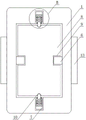
FIG. 1 is a front sectional view of the structure of the present invention;
FIG. 2 is an enlarged view of part A of the structure of FIG. 1;
FIG. 3 is a top cross-sectional view of the connection structure of the clamping member and the mounting hole of the present invention;
fig. 4 is an enlarged view of a portion B in fig. 3 according to the present invention.
The reference numbers in the figures illustrate:
1. a package housing; 2. a lead frame; 3. a placement groove; 4. mounting a chip; 5. connecting the solder balls; 6. positioning blocks; 7. a clamping member; 701. a clamping cylinder; 702. a damping block; 703. a movable insert block; 704. an elastic spring; 8. connecting the cover plate; 9. positioning a groove; 10. mounting holes; 11. a heat dissipating member; 111. a heat dissipating block; 112. a heat release groove; 12. a heat sink; 13. a heat conductive sheet; 14. a heat-conducting silica gel sheet.
Detailed Description
The technical solutions in the embodiments of the present invention will be described clearly and completely with reference to the accompanying drawings in the embodiments of the present invention, and it is obvious that the described embodiments are only some embodiments of the present invention, not all embodiments. Based on the embodiments in the present invention, all other embodiments obtained by a person skilled in the art without creative work belong to the protection scope of the present invention.
Referring to fig. 1-4, a semiconductor package structure comprises a package housing 1, lead frames 2 are fixedly connected to the left and right sides of the bottom of the package housing 1, a placement groove 3 is formed on the top of the package housing 1, an installation chip 4 is placed inside the placement groove 3, connection solder balls 5 are welded to the left and right sides of the bottom of the installation chip 4, the tops of the two lead frames 2 penetrate and extend into the placement groove 3, the two connection solder balls 5 are respectively welded to the tops of the two lead frames 2, positioning blocks 6 are fixedly mounted on the left and right sides of the placement groove 3, clamping members 7 are embedded in the front and the other sides of the placement groove 3, a connection cover plate 8 is clamped to the top of the placement groove 3, positioning grooves 9 are fixedly mounted on the left and right sides of the connection cover plate 8, one sides of the two positioning blocks 6 opposite to each extend and are clamped to the insides of the two positioning grooves 9, two joint component 7 one sides relative extend respectively and insert and connect to the inside of two mounting holes 10, the bottom fixed mounting of connection apron 8 has heat dissipation part 11, the bottom and the installation chip 4 contact of heat dissipation part 11, through install lead frame 2 in encapsulation shell 1 bottom, standing groove 3 has been seted up at the top, make installation chip 4 accessible connect tin ball 5, weld to two lead frames 2 in, standing groove 3 encapsulates standing groove 3 through connection apron 8, and the bottom of connection apron 8 installs heat dissipation part 11, can be directly with installation chip 4 contact, thereby better carry out heat conduction to installation chip 4, it is relatively better to make the device reach packaging structure's radiating effect, thereby electronic component's performance has been increased, reliability and life.
Preferably, the bottom of the package housing 1 is provided with a heat dissipation groove 12, the top of the heat dissipation groove 12 is communicated with the placement groove 3, the mounting chip 4 is located at the top of the heat dissipation groove 12, and the heat dissipation groove 12 is formed in the bottom of the package housing 1, so that the heat dissipation groove 12 ventilates the bottom of the mounting chip 4, and the heat dissipation effect of the device is further improved.
Preferably, the equal fixedly connected with conducting strip 13 in the left and right sides of encapsulation shell 1, one side that two conducting strips 13 are relative all runs through to in the standing groove 3, two conducting strips 13 respectively with the left and right sides contact of installation chip 4, the equal fixedly connected with conducting strip 13 in the left and right sides through encapsulation shell 1, make two conducting strips 13 can carry out the heat conduction to the left and right sides of installation chip 4, make the heat conduction effect of device better relatively, and the silica gel heat conduction pad is installed to one side that two conducting strips 13 are relative, conducting strip 13 is when the heat conduction, difficult damage installation chip 4, increase the practicality of device.
Preferably, the bottom of the heat dissipation part 11 is bonded with the heat-conducting silicone sheet 14, the bottom of the heat-conducting silicone sheet 14 is in contact with the mounting chip 4, and the heat-conducting silicone sheet 14 is bonded at the bottom of the heat dissipation part 11, so that the heat dissipation part 11 is not in hard contact with the mounting chip 4, the heat-conducting silicone sheet 14 has the function of protecting the mounting chip 4 while having heat conduction capacity, and the practicability and the service life of the device are further improved.
Preferably, the two clamping members 7 each include a clamping tube 701, the two clamping tubes 701 are each embedded in the top of the package housing 1, one opposite sides of the two clamping tubes 701 each penetrate into the placement groove 3, the interiors of the two clamping tubes 701 are each slidably connected with a damping block 702, one opposite side of each of the two damping blocks 702 is each fixedly connected with a movable insertion block 703, one end of each movable insertion block 703, which is far away from the damping block 702, penetrates and is slidably connected to the exterior of the clamping tube 701, an elastic spring 704 is fixedly installed between the damping block 702 and the clamping tube 701, the elastic spring 704 is sleeved on the movable insertion block 703, the clamping members 7 each include a clamping tube 701, a damping block 702, a movable insertion block 703 and an elastic spring 704, the clamping tubes 701 can support the damping block 702 and the movable insertion block 703, so that the movable insertion blocks 703 can be stably inserted into the installation holes 10 when the movable insertion blocks 703 receive the elastic force of the elastic springs 704, the stability of the device is increased.
Preferably, the heat dissipation part 11 includes the heat dissipation block 111, the top of the heat dissipation block 111 and the connection cover plate 8 are fixedly connected, the top of the heat dissipation block 111 is provided with heat release grooves 112 arranged equidistantly, the bottom of the heat dissipation block 111 is bonded with the heat conducting silicone sheet 14, the heat dissipation part 11 includes the heat dissipation block 111 and the heat release grooves 112 by setting, after the heat dissipation block 111 absorbs heat, the heat can be conducted by the heat release grooves 112, and then the heat is discharged, and the practicability of the device is improved.
The working principle is as follows: the lead frames 2 are arranged at the bottom of the packaging shell 1, the placing grooves 3 are arranged at the top, so that the mounting chips 4 can be welded into the two lead frames 2 through the connecting solder balls 5, the placing grooves 3 package the placing grooves 3 through the connecting cover plate 8, the heat dissipation parts 11 are arranged at the bottom of the connecting cover plate 8 and can be directly contacted with the mounting chips 4, so that the heat conduction of the mounting chips 4 is better performed, the positioning grooves 9 and the mounting holes 10 are arranged on the connecting cover plate 8, so that the positioning blocks 6 and the clamping components 7 on the placing grooves 3 can be respectively clamped into the positioning grooves 9 and the mounting holes 10, the connection and the mounting of the connecting cover plate 8 are relatively stable, the structure of the device is relatively simple, the packaging is relatively convenient, the heat dissipation effect of the device reaching the packaging structure is relatively good, the performance, the reliability and the service life of electronic elements are improved, and the problem that the heat, the problems of performance, reliability and average lifetime of electronic components are reduced.
It is noted that, herein, relational terms such as first and second, and the like may be used solely to distinguish one entity or action from another entity or action without necessarily requiring or implying any actual such relationship or order between such entities or actions. Also, the terms "comprises," "comprising," or any other variation thereof, are intended to cover a non-exclusive inclusion, such that a process, method, article, or apparatus that comprises a list of elements does not include only those elements but may include other elements not expressly listed or inherent to such process, method, article, or apparatus. Without further limitation, an element defined by the phrase "comprising an … …" does not exclude the presence of other identical elements in a process, method, article, or apparatus that comprises the element.
Although embodiments of the present invention have been shown and described, it will be appreciated by those skilled in the art that changes, modifications, substitutions and alterations can be made in these embodiments without departing from the principles and spirit of the invention, the scope of which is defined in the appended claims and their equivalents.
Claims (6)
1. A semiconductor package structure, including encapsulation shell (1), its characterized in that: encapsulation shell (1) bottom left and right sides fixedly connected with lead frame (2), standing groove (3) have been seted up at the top of encapsulation shell (1), standing groove (3) internally placed installs chip (4), the equal welding in the left and right sides of installation chip (4) bottom has connection tin ball (5), two the inside that runs through and extend to standing groove (3) in the top of lead frame (2), two connect tin ball (5) respectively with the top welding of two lead frames (2), the equal fixed mounting in the left and right sides of standing groove (3) has locating piece (6), the front of standing groove (3) all inlays with other face and is equipped with joint component (7), the top joint of standing groove (3) has connection cover plate (8), the left and right sides fixed mounting of connection cover plate (8) has constant head tank (9), two the relative one side of locating piece (6) extends respectively and the joint to the interior of two constant head tanks (9) The connecting cover plate comprises a connecting cover plate body (8), wherein mounting holes (10) are formed in the front face and the back face of the connecting cover plate body (8), two clamping components (7) extend to the opposite sides of the clamping components respectively and are inserted into the two mounting holes (10), a heat dissipation component (11) is fixedly mounted at the bottom of the connecting cover plate body (8), and the bottom of the heat dissipation component (11) is in contact with an installation chip (4).
2. The semiconductor package structure of claim 1, wherein: the packaging structure is characterized in that a heat dissipation groove (12) is formed in the bottom of the packaging shell (1), the top of the heat dissipation groove (12) is communicated with the placing groove (3), and the installation chip (4) is located at the top of the heat dissipation groove (12).
3. The semiconductor package structure of claim 1, wherein: the packaging structure is characterized in that heat-conducting fins (13) are fixedly connected to the left side and the right side of the packaging shell (1), one opposite side of each heat-conducting fin (13) penetrates into the placing groove (3), and the two heat-conducting fins (13) are respectively in contact with the left side and the right side of the mounting chip (4).
4. The semiconductor package structure of claim 1, wherein: the bottom of the heat dissipation part (11) is bonded with a heat conduction silica gel sheet (14), and the bottom of the heat conduction silica gel sheet (14) is in contact with the mounting chip (4).
5. The semiconductor package structure of claim 1, wherein: two joint component (7) all include a joint section of thick bamboo (701), two joint section of thick bamboo (701) all inlays and locates the top of encapsulation shell (1), two in one side that joint section of thick bamboo (701) is relative all runs through to standing groove (3), two the equal sliding connection in inside of a joint section of thick bamboo (701) has damping piece (702), two equal fixedly connected with activity inserted block (703), two the one end that damping piece (702) were kept away from in activity inserted block (703) runs through and sliding connection to the outside of a joint section of thick bamboo (701), fixed mounting has elastic spring (704) between damping piece (702) and a joint section of thick bamboo (701), elastic spring (704) cover is located on activity inserted block (703).
6. The semiconductor package structure of claim 4, wherein: the heat dissipation part (11) comprises a heat dissipation block (111), the top of the heat dissipation block (111) is fixedly connected with the connecting cover plate (8), heat dissipation grooves (112) which are arranged equidistantly are formed in the top of the heat dissipation block (111), and the bottom of the heat dissipation block (111) is bonded with the heat conduction silica gel sheet (14).
Priority Applications (1)
| Application Number | Priority Date | Filing Date | Title |
|---|---|---|---|
| CN202021167861.6U CN212033009U (en) | 2020-06-22 | 2020-06-22 | Semiconductor packaging structure |
Applications Claiming Priority (1)
| Application Number | Priority Date | Filing Date | Title |
|---|---|---|---|
| CN202021167861.6U CN212033009U (en) | 2020-06-22 | 2020-06-22 | Semiconductor packaging structure |
Publications (1)
| Publication Number | Publication Date |
|---|---|
| CN212033009U true CN212033009U (en) | 2020-11-27 |
Family
ID=73477390
Family Applications (1)
| Application Number | Title | Priority Date | Filing Date |
|---|---|---|---|
| CN202021167861.6U Active CN212033009U (en) | 2020-06-22 | 2020-06-22 | Semiconductor packaging structure |
Country Status (1)
| Country | Link |
|---|---|
| CN (1) | CN212033009U (en) |
Cited By (2)
| Publication number | Priority date | Publication date | Assignee | Title |
|---|---|---|---|---|
| CN117727700A (en) * | 2024-02-07 | 2024-03-19 | 苏州熹联光芯微电子科技有限公司 | Chip packaging structure |
| CN118610178A (en) * | 2024-07-31 | 2024-09-06 | 江苏晟驰微电子有限公司 | DFN power device with interconnection structure for conductive silver wire |
-
2020
- 2020-06-22 CN CN202021167861.6U patent/CN212033009U/en active Active
Cited By (3)
| Publication number | Priority date | Publication date | Assignee | Title |
|---|---|---|---|---|
| CN117727700A (en) * | 2024-02-07 | 2024-03-19 | 苏州熹联光芯微电子科技有限公司 | Chip packaging structure |
| CN117727700B (en) * | 2024-02-07 | 2024-05-03 | 苏州熹联光芯微电子科技有限公司 | Chip packaging structure |
| CN118610178A (en) * | 2024-07-31 | 2024-09-06 | 江苏晟驰微电子有限公司 | DFN power device with interconnection structure for conductive silver wire |
Similar Documents
| Publication | Publication Date | Title |
|---|---|---|
| US7709951B2 (en) | Thermal pillow | |
| CN212033009U (en) | Semiconductor packaging structure | |
| US20120224339A1 (en) | Terminal box for use with solar cell module and method of manufacturing the terminal box | |
| CN211184790U (en) | Electric bicycle lithium cell heat radiation structure | |
| CN209785753U (en) | Capacitor with protection device | |
| CN207637783U (en) | A kind of high power semiconductor base plate for packaging and semiconductor package | |
| CN110473849B (en) | SMD diode of firm type of heat conduction | |
| CN210956663U (en) | Firm SMD diode takes precautions against earthquakes | |
| CN114927485A (en) | Electric conduction, heat storage and heat transfer method for components | |
| CN210073824U (en) | Heat dissipation mainboard and optical module | |
| CN220895496U (en) | Semiconductor device with reverse pins | |
| CN111465268A (en) | Radiator and manufacturing method thereof and electronic equipment | |
| CN210271941U (en) | Chip resistor substrate structure | |
| CN219552710U (en) | Photoelectric connection structure | |
| CN220510004U (en) | Semiconductor shell with good waterproof performance | |
| CN218888766U (en) | Hybrid packaging structure of integrated circuit chip | |
| CN211719574U (en) | Paster diode component easy to install | |
| CN213583756U (en) | Electronic chip packaging structure | |
| CN213151722U (en) | PCBA with wireless power supply module | |
| CN218526489U (en) | High heat dissipation chip plate body structure | |
| CN219226275U (en) | TVS tube with good heat dissipation performance | |
| CN211402842U (en) | Anti-electrostatic interference heat dissipation structure of optical module | |
| CN214226906U (en) | Chip heat radiation structure, packaged chip and electronic equipment | |
| CN217280846U (en) | Multi-chip module packaging structure | |
| CN220753407U (en) | Power tube assembly and PCB assembly |
Legal Events
| Date | Code | Title | Description |
|---|---|---|---|
| GR01 | Patent grant | ||
| GR01 | Patent grant |