CN1622304A - Flip chip bonding method and layered metal architecture of substrate for stud bump - Google Patents
Flip chip bonding method and layered metal architecture of substrate for stud bump Download PDFInfo
- Publication number
- CN1622304A CN1622304A CNA2004100803660A CN200410080366A CN1622304A CN 1622304 A CN1622304 A CN 1622304A CN A2004100803660 A CNA2004100803660 A CN A2004100803660A CN 200410080366 A CN200410080366 A CN 200410080366A CN 1622304 A CN1622304 A CN 1622304A
- Authority
- CN
- China
- Prior art keywords
- chip
- substrate
- projection
- stud bump
- ultrasonic wave
- Prior art date
- Legal status (The legal status is an assumption and is not a legal conclusion. Google has not performed a legal analysis and makes no representation as to the accuracy of the status listed.)
- Pending
Links
Images


Classifications
-
- H—ELECTRICITY
- H01—ELECTRIC ELEMENTS
- H01L—SEMICONDUCTOR DEVICES NOT COVERED BY CLASS H10
- H01L24/00—Arrangements for connecting or disconnecting semiconductor or solid-state bodies; Methods or apparatus related thereto
- H01L24/80—Methods for connecting semiconductor or other solid state bodies using means for bonding being attached to, or being formed on, the surface to be connected
- H01L24/81—Methods for connecting semiconductor or other solid state bodies using means for bonding being attached to, or being formed on, the surface to be connected using a bump connector
-
- H—ELECTRICITY
- H01—ELECTRIC ELEMENTS
- H01L—SEMICONDUCTOR DEVICES NOT COVERED BY CLASS H10
- H01L21/00—Processes or apparatus adapted for the manufacture or treatment of semiconductor or solid state devices or of parts thereof
- H01L21/02—Manufacture or treatment of semiconductor devices or of parts thereof
- H01L21/04—Manufacture or treatment of semiconductor devices or of parts thereof the devices having at least one potential-jump barrier or surface barrier, e.g. PN junction, depletion layer or carrier concentration layer
- H01L21/50—Assembly of semiconductor devices using processes or apparatus not provided for in a single one of the subgroups H01L21/06 - H01L21/326, e.g. sealing of a cap to a base of a container
- H01L21/56—Encapsulations, e.g. encapsulation layers, coatings
- H01L21/563—Encapsulation of active face of flip-chip device, e.g. underfilling or underencapsulation of flip-chip, encapsulation preform on chip or mounting substrate
-
- H—ELECTRICITY
- H01—ELECTRIC ELEMENTS
- H01L—SEMICONDUCTOR DEVICES NOT COVERED BY CLASS H10
- H01L21/00—Processes or apparatus adapted for the manufacture or treatment of semiconductor or solid state devices or of parts thereof
- H01L21/02—Manufacture or treatment of semiconductor devices or of parts thereof
- H01L21/04—Manufacture or treatment of semiconductor devices or of parts thereof the devices having at least one potential-jump barrier or surface barrier, e.g. PN junction, depletion layer or carrier concentration layer
- H01L21/50—Assembly of semiconductor devices using processes or apparatus not provided for in a single one of the subgroups H01L21/06 - H01L21/326, e.g. sealing of a cap to a base of a container
- H01L21/60—Attaching or detaching leads or other conductive members, to be used for carrying current to or from the device in operation
-
- H—ELECTRICITY
- H01—ELECTRIC ELEMENTS
- H01L—SEMICONDUCTOR DEVICES NOT COVERED BY CLASS H10
- H01L24/00—Arrangements for connecting or disconnecting semiconductor or solid-state bodies; Methods or apparatus related thereto
- H01L24/01—Means for bonding being attached to, or being formed on, the surface to be connected, e.g. chip-to-package, die-attach, "first-level" interconnects; Manufacturing methods related thereto
- H01L24/26—Layer connectors, e.g. plate connectors, solder or adhesive layers; Manufacturing methods related thereto
- H01L24/28—Structure, shape, material or disposition of the layer connectors prior to the connecting process
- H01L24/29—Structure, shape, material or disposition of the layer connectors prior to the connecting process of an individual layer connector
-
- H—ELECTRICITY
- H01—ELECTRIC ELEMENTS
- H01L—SEMICONDUCTOR DEVICES NOT COVERED BY CLASS H10
- H01L24/00—Arrangements for connecting or disconnecting semiconductor or solid-state bodies; Methods or apparatus related thereto
- H01L24/01—Means for bonding being attached to, or being formed on, the surface to be connected, e.g. chip-to-package, die-attach, "first-level" interconnects; Manufacturing methods related thereto
- H01L24/26—Layer connectors, e.g. plate connectors, solder or adhesive layers; Manufacturing methods related thereto
- H01L24/31—Structure, shape, material or disposition of the layer connectors after the connecting process
-
- H—ELECTRICITY
- H01—ELECTRIC ELEMENTS
- H01L—SEMICONDUCTOR DEVICES NOT COVERED BY CLASS H10
- H01L2224/00—Indexing scheme for arrangements for connecting or disconnecting semiconductor or solid-state bodies and methods related thereto as covered by H01L24/00
- H01L2224/01—Means for bonding being attached to, or being formed on, the surface to be connected, e.g. chip-to-package, die-attach, "first-level" interconnects; Manufacturing methods related thereto
- H01L2224/02—Bonding areas; Manufacturing methods related thereto
- H01L2224/04—Structure, shape, material or disposition of the bonding areas prior to the connecting process
- H01L2224/05—Structure, shape, material or disposition of the bonding areas prior to the connecting process of an individual bonding area
- H01L2224/05001—Internal layers
- H01L2224/05099—Material
- H01L2224/051—Material with a principal constituent of the material being a metal or a metalloid, e.g. boron [B], silicon [Si], germanium [Ge], arsenic [As], antimony [Sb], tellurium [Te] and polonium [Po], and alloys thereof
- H01L2224/05117—Material with a principal constituent of the material being a metal or a metalloid, e.g. boron [B], silicon [Si], germanium [Ge], arsenic [As], antimony [Sb], tellurium [Te] and polonium [Po], and alloys thereof the principal constituent melting at a temperature of greater than or equal to 400°C and less than 950°C
- H01L2224/05124—Aluminium [Al] as principal constituent
-
- H—ELECTRICITY
- H01—ELECTRIC ELEMENTS
- H01L—SEMICONDUCTOR DEVICES NOT COVERED BY CLASS H10
- H01L2224/00—Indexing scheme for arrangements for connecting or disconnecting semiconductor or solid-state bodies and methods related thereto as covered by H01L24/00
- H01L2224/01—Means for bonding being attached to, or being formed on, the surface to be connected, e.g. chip-to-package, die-attach, "first-level" interconnects; Manufacturing methods related thereto
- H01L2224/02—Bonding areas; Manufacturing methods related thereto
- H01L2224/04—Structure, shape, material or disposition of the bonding areas prior to the connecting process
- H01L2224/05—Structure, shape, material or disposition of the bonding areas prior to the connecting process of an individual bonding area
- H01L2224/0554—External layer
- H01L2224/0556—Disposition
- H01L2224/05571—Disposition the external layer being disposed in a recess of the surface
-
- H—ELECTRICITY
- H01—ELECTRIC ELEMENTS
- H01L—SEMICONDUCTOR DEVICES NOT COVERED BY CLASS H10
- H01L2224/00—Indexing scheme for arrangements for connecting or disconnecting semiconductor or solid-state bodies and methods related thereto as covered by H01L24/00
- H01L2224/01—Means for bonding being attached to, or being formed on, the surface to be connected, e.g. chip-to-package, die-attach, "first-level" interconnects; Manufacturing methods related thereto
- H01L2224/02—Bonding areas; Manufacturing methods related thereto
- H01L2224/04—Structure, shape, material or disposition of the bonding areas prior to the connecting process
- H01L2224/05—Structure, shape, material or disposition of the bonding areas prior to the connecting process of an individual bonding area
- H01L2224/0554—External layer
- H01L2224/05573—Single external layer
-
- H—ELECTRICITY
- H01—ELECTRIC ELEMENTS
- H01L—SEMICONDUCTOR DEVICES NOT COVERED BY CLASS H10
- H01L2224/00—Indexing scheme for arrangements for connecting or disconnecting semiconductor or solid-state bodies and methods related thereto as covered by H01L24/00
- H01L2224/01—Means for bonding being attached to, or being formed on, the surface to be connected, e.g. chip-to-package, die-attach, "first-level" interconnects; Manufacturing methods related thereto
- H01L2224/02—Bonding areas; Manufacturing methods related thereto
- H01L2224/04—Structure, shape, material or disposition of the bonding areas prior to the connecting process
- H01L2224/05—Structure, shape, material or disposition of the bonding areas prior to the connecting process of an individual bonding area
- H01L2224/0554—External layer
- H01L2224/05599—Material
- H01L2224/056—Material with a principal constituent of the material being a metal or a metalloid, e.g. boron [B], silicon [Si], germanium [Ge], arsenic [As], antimony [Sb], tellurium [Te] and polonium [Po], and alloys thereof
- H01L2224/05617—Material with a principal constituent of the material being a metal or a metalloid, e.g. boron [B], silicon [Si], germanium [Ge], arsenic [As], antimony [Sb], tellurium [Te] and polonium [Po], and alloys thereof the principal constituent melting at a temperature of greater than or equal to 400°C and less than 950°C
- H01L2224/05624—Aluminium [Al] as principal constituent
-
- H—ELECTRICITY
- H01—ELECTRIC ELEMENTS
- H01L—SEMICONDUCTOR DEVICES NOT COVERED BY CLASS H10
- H01L2224/00—Indexing scheme for arrangements for connecting or disconnecting semiconductor or solid-state bodies and methods related thereto as covered by H01L24/00
- H01L2224/01—Means for bonding being attached to, or being formed on, the surface to be connected, e.g. chip-to-package, die-attach, "first-level" interconnects; Manufacturing methods related thereto
- H01L2224/10—Bump connectors; Manufacturing methods related thereto
- H01L2224/11—Manufacturing methods
- H01L2224/113—Manufacturing methods by local deposition of the material of the bump connector
- H01L2224/1133—Manufacturing methods by local deposition of the material of the bump connector in solid form
- H01L2224/1134—Stud bumping, i.e. using a wire-bonding apparatus
-
- H—ELECTRICITY
- H01—ELECTRIC ELEMENTS
- H01L—SEMICONDUCTOR DEVICES NOT COVERED BY CLASS H10
- H01L2224/00—Indexing scheme for arrangements for connecting or disconnecting semiconductor or solid-state bodies and methods related thereto as covered by H01L24/00
- H01L2224/01—Means for bonding being attached to, or being formed on, the surface to be connected, e.g. chip-to-package, die-attach, "first-level" interconnects; Manufacturing methods related thereto
- H01L2224/10—Bump connectors; Manufacturing methods related thereto
- H01L2224/12—Structure, shape, material or disposition of the bump connectors prior to the connecting process
- H01L2224/13—Structure, shape, material or disposition of the bump connectors prior to the connecting process of an individual bump connector
- H01L2224/13001—Core members of the bump connector
- H01L2224/13099—Material
- H01L2224/131—Material with a principal constituent of the material being a metal or a metalloid, e.g. boron [B], silicon [Si], germanium [Ge], arsenic [As], antimony [Sb], tellurium [Te] and polonium [Po], and alloys thereof
- H01L2224/13138—Material with a principal constituent of the material being a metal or a metalloid, e.g. boron [B], silicon [Si], germanium [Ge], arsenic [As], antimony [Sb], tellurium [Te] and polonium [Po], and alloys thereof the principal constituent melting at a temperature of greater than or equal to 950°C and less than 1550°C
- H01L2224/13144—Gold [Au] as principal constituent
-
- H—ELECTRICITY
- H01—ELECTRIC ELEMENTS
- H01L—SEMICONDUCTOR DEVICES NOT COVERED BY CLASS H10
- H01L2224/00—Indexing scheme for arrangements for connecting or disconnecting semiconductor or solid-state bodies and methods related thereto as covered by H01L24/00
- H01L2224/01—Means for bonding being attached to, or being formed on, the surface to be connected, e.g. chip-to-package, die-attach, "first-level" interconnects; Manufacturing methods related thereto
- H01L2224/10—Bump connectors; Manufacturing methods related thereto
- H01L2224/12—Structure, shape, material or disposition of the bump connectors prior to the connecting process
- H01L2224/13—Structure, shape, material or disposition of the bump connectors prior to the connecting process of an individual bump connector
- H01L2224/13001—Core members of the bump connector
- H01L2224/13099—Material
- H01L2224/131—Material with a principal constituent of the material being a metal or a metalloid, e.g. boron [B], silicon [Si], germanium [Ge], arsenic [As], antimony [Sb], tellurium [Te] and polonium [Po], and alloys thereof
- H01L2224/13138—Material with a principal constituent of the material being a metal or a metalloid, e.g. boron [B], silicon [Si], germanium [Ge], arsenic [As], antimony [Sb], tellurium [Te] and polonium [Po], and alloys thereof the principal constituent melting at a temperature of greater than or equal to 950°C and less than 1550°C
- H01L2224/13147—Copper [Cu] as principal constituent
-
- H—ELECTRICITY
- H01—ELECTRIC ELEMENTS
- H01L—SEMICONDUCTOR DEVICES NOT COVERED BY CLASS H10
- H01L2224/00—Indexing scheme for arrangements for connecting or disconnecting semiconductor or solid-state bodies and methods related thereto as covered by H01L24/00
- H01L2224/01—Means for bonding being attached to, or being formed on, the surface to be connected, e.g. chip-to-package, die-attach, "first-level" interconnects; Manufacturing methods related thereto
- H01L2224/10—Bump connectors; Manufacturing methods related thereto
- H01L2224/15—Structure, shape, material or disposition of the bump connectors after the connecting process
- H01L2224/16—Structure, shape, material or disposition of the bump connectors after the connecting process of an individual bump connector
- H01L2224/161—Disposition
- H01L2224/16135—Disposition the bump connector connecting between different semiconductor or solid-state bodies, i.e. chip-to-chip
- H01L2224/16145—Disposition the bump connector connecting between different semiconductor or solid-state bodies, i.e. chip-to-chip the bodies being stacked
-
- H—ELECTRICITY
- H01—ELECTRIC ELEMENTS
- H01L—SEMICONDUCTOR DEVICES NOT COVERED BY CLASS H10
- H01L2224/00—Indexing scheme for arrangements for connecting or disconnecting semiconductor or solid-state bodies and methods related thereto as covered by H01L24/00
- H01L2224/01—Means for bonding being attached to, or being formed on, the surface to be connected, e.g. chip-to-package, die-attach, "first-level" interconnects; Manufacturing methods related thereto
- H01L2224/10—Bump connectors; Manufacturing methods related thereto
- H01L2224/15—Structure, shape, material or disposition of the bump connectors after the connecting process
- H01L2224/16—Structure, shape, material or disposition of the bump connectors after the connecting process of an individual bump connector
- H01L2224/161—Disposition
- H01L2224/16151—Disposition the bump connector connecting between a semiconductor or solid-state body and an item not being a semiconductor or solid-state body, e.g. chip-to-substrate, chip-to-passive
- H01L2224/16221—Disposition the bump connector connecting between a semiconductor or solid-state body and an item not being a semiconductor or solid-state body, e.g. chip-to-substrate, chip-to-passive the body and the item being stacked
- H01L2224/16225—Disposition the bump connector connecting between a semiconductor or solid-state body and an item not being a semiconductor or solid-state body, e.g. chip-to-substrate, chip-to-passive the body and the item being stacked the item being non-metallic, e.g. insulating substrate with or without metallisation
-
- H—ELECTRICITY
- H01—ELECTRIC ELEMENTS
- H01L—SEMICONDUCTOR DEVICES NOT COVERED BY CLASS H10
- H01L2224/00—Indexing scheme for arrangements for connecting or disconnecting semiconductor or solid-state bodies and methods related thereto as covered by H01L24/00
- H01L2224/01—Means for bonding being attached to, or being formed on, the surface to be connected, e.g. chip-to-package, die-attach, "first-level" interconnects; Manufacturing methods related thereto
- H01L2224/26—Layer connectors, e.g. plate connectors, solder or adhesive layers; Manufacturing methods related thereto
- H01L2224/31—Structure, shape, material or disposition of the layer connectors after the connecting process
- H01L2224/32—Structure, shape, material or disposition of the layer connectors after the connecting process of an individual layer connector
- H01L2224/321—Disposition
- H01L2224/32135—Disposition the layer connector connecting between different semiconductor or solid-state bodies, i.e. chip-to-chip
- H01L2224/32145—Disposition the layer connector connecting between different semiconductor or solid-state bodies, i.e. chip-to-chip the bodies being stacked
-
- H—ELECTRICITY
- H01—ELECTRIC ELEMENTS
- H01L—SEMICONDUCTOR DEVICES NOT COVERED BY CLASS H10
- H01L2224/00—Indexing scheme for arrangements for connecting or disconnecting semiconductor or solid-state bodies and methods related thereto as covered by H01L24/00
- H01L2224/01—Means for bonding being attached to, or being formed on, the surface to be connected, e.g. chip-to-package, die-attach, "first-level" interconnects; Manufacturing methods related thereto
- H01L2224/26—Layer connectors, e.g. plate connectors, solder or adhesive layers; Manufacturing methods related thereto
- H01L2224/31—Structure, shape, material or disposition of the layer connectors after the connecting process
- H01L2224/32—Structure, shape, material or disposition of the layer connectors after the connecting process of an individual layer connector
- H01L2224/321—Disposition
- H01L2224/32151—Disposition the layer connector connecting between a semiconductor or solid-state body and an item not being a semiconductor or solid-state body, e.g. chip-to-substrate, chip-to-passive
- H01L2224/32221—Disposition the layer connector connecting between a semiconductor or solid-state body and an item not being a semiconductor or solid-state body, e.g. chip-to-substrate, chip-to-passive the body and the item being stacked
- H01L2224/32225—Disposition the layer connector connecting between a semiconductor or solid-state body and an item not being a semiconductor or solid-state body, e.g. chip-to-substrate, chip-to-passive the body and the item being stacked the item being non-metallic, e.g. insulating substrate with or without metallisation
-
- H—ELECTRICITY
- H01—ELECTRIC ELEMENTS
- H01L—SEMICONDUCTOR DEVICES NOT COVERED BY CLASS H10
- H01L2224/00—Indexing scheme for arrangements for connecting or disconnecting semiconductor or solid-state bodies and methods related thereto as covered by H01L24/00
- H01L2224/01—Means for bonding being attached to, or being formed on, the surface to be connected, e.g. chip-to-package, die-attach, "first-level" interconnects; Manufacturing methods related thereto
- H01L2224/42—Wire connectors; Manufacturing methods related thereto
- H01L2224/44—Structure, shape, material or disposition of the wire connectors prior to the connecting process
- H01L2224/45—Structure, shape, material or disposition of the wire connectors prior to the connecting process of an individual wire connector
- H01L2224/45001—Core members of the connector
- H01L2224/45099—Material
- H01L2224/451—Material with a principal constituent of the material being a metal or a metalloid, e.g. boron (B), silicon (Si), germanium (Ge), arsenic (As), antimony (Sb), tellurium (Te) and polonium (Po), and alloys thereof
- H01L2224/45117—Material with a principal constituent of the material being a metal or a metalloid, e.g. boron (B), silicon (Si), germanium (Ge), arsenic (As), antimony (Sb), tellurium (Te) and polonium (Po), and alloys thereof the principal constituent melting at a temperature of greater than or equal to 400°C and less than 950°C
- H01L2224/45124—Aluminium (Al) as principal constituent
-
- H—ELECTRICITY
- H01—ELECTRIC ELEMENTS
- H01L—SEMICONDUCTOR DEVICES NOT COVERED BY CLASS H10
- H01L2224/00—Indexing scheme for arrangements for connecting or disconnecting semiconductor or solid-state bodies and methods related thereto as covered by H01L24/00
- H01L2224/01—Means for bonding being attached to, or being formed on, the surface to be connected, e.g. chip-to-package, die-attach, "first-level" interconnects; Manufacturing methods related thereto
- H01L2224/42—Wire connectors; Manufacturing methods related thereto
- H01L2224/44—Structure, shape, material or disposition of the wire connectors prior to the connecting process
- H01L2224/45—Structure, shape, material or disposition of the wire connectors prior to the connecting process of an individual wire connector
- H01L2224/45001—Core members of the connector
- H01L2224/45099—Material
- H01L2224/451—Material with a principal constituent of the material being a metal or a metalloid, e.g. boron (B), silicon (Si), germanium (Ge), arsenic (As), antimony (Sb), tellurium (Te) and polonium (Po), and alloys thereof
- H01L2224/45138—Material with a principal constituent of the material being a metal or a metalloid, e.g. boron (B), silicon (Si), germanium (Ge), arsenic (As), antimony (Sb), tellurium (Te) and polonium (Po), and alloys thereof the principal constituent melting at a temperature of greater than or equal to 950°C and less than 1550°C
- H01L2224/45139—Silver (Ag) as principal constituent
-
- H—ELECTRICITY
- H01—ELECTRIC ELEMENTS
- H01L—SEMICONDUCTOR DEVICES NOT COVERED BY CLASS H10
- H01L2224/00—Indexing scheme for arrangements for connecting or disconnecting semiconductor or solid-state bodies and methods related thereto as covered by H01L24/00
- H01L2224/01—Means for bonding being attached to, or being formed on, the surface to be connected, e.g. chip-to-package, die-attach, "first-level" interconnects; Manufacturing methods related thereto
- H01L2224/42—Wire connectors; Manufacturing methods related thereto
- H01L2224/44—Structure, shape, material or disposition of the wire connectors prior to the connecting process
- H01L2224/45—Structure, shape, material or disposition of the wire connectors prior to the connecting process of an individual wire connector
- H01L2224/45001—Core members of the connector
- H01L2224/45099—Material
- H01L2224/451—Material with a principal constituent of the material being a metal or a metalloid, e.g. boron (B), silicon (Si), germanium (Ge), arsenic (As), antimony (Sb), tellurium (Te) and polonium (Po), and alloys thereof
- H01L2224/45138—Material with a principal constituent of the material being a metal or a metalloid, e.g. boron (B), silicon (Si), germanium (Ge), arsenic (As), antimony (Sb), tellurium (Te) and polonium (Po), and alloys thereof the principal constituent melting at a temperature of greater than or equal to 950°C and less than 1550°C
- H01L2224/45144—Gold (Au) as principal constituent
-
- H—ELECTRICITY
- H01—ELECTRIC ELEMENTS
- H01L—SEMICONDUCTOR DEVICES NOT COVERED BY CLASS H10
- H01L2224/00—Indexing scheme for arrangements for connecting or disconnecting semiconductor or solid-state bodies and methods related thereto as covered by H01L24/00
- H01L2224/01—Means for bonding being attached to, or being formed on, the surface to be connected, e.g. chip-to-package, die-attach, "first-level" interconnects; Manufacturing methods related thereto
- H01L2224/42—Wire connectors; Manufacturing methods related thereto
- H01L2224/44—Structure, shape, material or disposition of the wire connectors prior to the connecting process
- H01L2224/45—Structure, shape, material or disposition of the wire connectors prior to the connecting process of an individual wire connector
- H01L2224/45001—Core members of the connector
- H01L2224/45099—Material
- H01L2224/451—Material with a principal constituent of the material being a metal or a metalloid, e.g. boron (B), silicon (Si), germanium (Ge), arsenic (As), antimony (Sb), tellurium (Te) and polonium (Po), and alloys thereof
- H01L2224/45138—Material with a principal constituent of the material being a metal or a metalloid, e.g. boron (B), silicon (Si), germanium (Ge), arsenic (As), antimony (Sb), tellurium (Te) and polonium (Po), and alloys thereof the principal constituent melting at a temperature of greater than or equal to 950°C and less than 1550°C
- H01L2224/45147—Copper (Cu) as principal constituent
-
- H—ELECTRICITY
- H01—ELECTRIC ELEMENTS
- H01L—SEMICONDUCTOR DEVICES NOT COVERED BY CLASS H10
- H01L2224/00—Indexing scheme for arrangements for connecting or disconnecting semiconductor or solid-state bodies and methods related thereto as covered by H01L24/00
- H01L2224/01—Means for bonding being attached to, or being formed on, the surface to be connected, e.g. chip-to-package, die-attach, "first-level" interconnects; Manufacturing methods related thereto
- H01L2224/42—Wire connectors; Manufacturing methods related thereto
- H01L2224/47—Structure, shape, material or disposition of the wire connectors after the connecting process
- H01L2224/48—Structure, shape, material or disposition of the wire connectors after the connecting process of an individual wire connector
- H01L2224/4805—Shape
- H01L2224/4809—Loop shape
- H01L2224/48095—Kinked
-
- H—ELECTRICITY
- H01—ELECTRIC ELEMENTS
- H01L—SEMICONDUCTOR DEVICES NOT COVERED BY CLASS H10
- H01L2224/00—Indexing scheme for arrangements for connecting or disconnecting semiconductor or solid-state bodies and methods related thereto as covered by H01L24/00
- H01L2224/01—Means for bonding being attached to, or being formed on, the surface to be connected, e.g. chip-to-package, die-attach, "first-level" interconnects; Manufacturing methods related thereto
- H01L2224/42—Wire connectors; Manufacturing methods related thereto
- H01L2224/47—Structure, shape, material or disposition of the wire connectors after the connecting process
- H01L2224/48—Structure, shape, material or disposition of the wire connectors after the connecting process of an individual wire connector
- H01L2224/484—Connecting portions
- H01L2224/48463—Connecting portions the connecting portion on the bonding area of the semiconductor or solid-state body being a ball bond
- H01L2224/48465—Connecting portions the connecting portion on the bonding area of the semiconductor or solid-state body being a ball bond the other connecting portion not on the bonding area being a wedge bond, i.e. ball-to-wedge, regular stitch
-
- H—ELECTRICITY
- H01—ELECTRIC ELEMENTS
- H01L—SEMICONDUCTOR DEVICES NOT COVERED BY CLASS H10
- H01L2224/00—Indexing scheme for arrangements for connecting or disconnecting semiconductor or solid-state bodies and methods related thereto as covered by H01L24/00
- H01L2224/73—Means for bonding being of different types provided for in two or more of groups H01L2224/10, H01L2224/18, H01L2224/26, H01L2224/34, H01L2224/42, H01L2224/50, H01L2224/63, H01L2224/71
- H01L2224/732—Location after the connecting process
- H01L2224/73201—Location after the connecting process on the same surface
- H01L2224/73203—Bump and layer connectors
- H01L2224/73204—Bump and layer connectors the bump connector being embedded into the layer connector
-
- H—ELECTRICITY
- H01—ELECTRIC ELEMENTS
- H01L—SEMICONDUCTOR DEVICES NOT COVERED BY CLASS H10
- H01L2224/00—Indexing scheme for arrangements for connecting or disconnecting semiconductor or solid-state bodies and methods related thereto as covered by H01L24/00
- H01L2224/73—Means for bonding being of different types provided for in two or more of groups H01L2224/10, H01L2224/18, H01L2224/26, H01L2224/34, H01L2224/42, H01L2224/50, H01L2224/63, H01L2224/71
- H01L2224/732—Location after the connecting process
- H01L2224/73201—Location after the connecting process on the same surface
- H01L2224/73207—Bump and wire connectors
-
- H—ELECTRICITY
- H01—ELECTRIC ELEMENTS
- H01L—SEMICONDUCTOR DEVICES NOT COVERED BY CLASS H10
- H01L2224/00—Indexing scheme for arrangements for connecting or disconnecting semiconductor or solid-state bodies and methods related thereto as covered by H01L24/00
- H01L2224/80—Methods for connecting semiconductor or other solid state bodies using means for bonding being attached to, or being formed on, the surface to be connected
- H01L2224/81—Methods for connecting semiconductor or other solid state bodies using means for bonding being attached to, or being formed on, the surface to be connected using a bump connector
- H01L2224/8119—Arrangement of the bump connectors prior to mounting
- H01L2224/81191—Arrangement of the bump connectors prior to mounting wherein the bump connectors are disposed only on the semiconductor or solid-state body
-
- H—ELECTRICITY
- H01—ELECTRIC ELEMENTS
- H01L—SEMICONDUCTOR DEVICES NOT COVERED BY CLASS H10
- H01L2224/00—Indexing scheme for arrangements for connecting or disconnecting semiconductor or solid-state bodies and methods related thereto as covered by H01L24/00
- H01L2224/80—Methods for connecting semiconductor or other solid state bodies using means for bonding being attached to, or being formed on, the surface to be connected
- H01L2224/81—Methods for connecting semiconductor or other solid state bodies using means for bonding being attached to, or being formed on, the surface to be connected using a bump connector
- H01L2224/8119—Arrangement of the bump connectors prior to mounting
- H01L2224/81193—Arrangement of the bump connectors prior to mounting wherein the bump connectors are disposed on both the semiconductor or solid-state body and another item or body to be connected to the semiconductor or solid-state body
-
- H—ELECTRICITY
- H01—ELECTRIC ELEMENTS
- H01L—SEMICONDUCTOR DEVICES NOT COVERED BY CLASS H10
- H01L2224/00—Indexing scheme for arrangements for connecting or disconnecting semiconductor or solid-state bodies and methods related thereto as covered by H01L24/00
- H01L2224/80—Methods for connecting semiconductor or other solid state bodies using means for bonding being attached to, or being formed on, the surface to be connected
- H01L2224/81—Methods for connecting semiconductor or other solid state bodies using means for bonding being attached to, or being formed on, the surface to be connected using a bump connector
- H01L2224/812—Applying energy for connecting
- H01L2224/81201—Compression bonding
- H01L2224/81205—Ultrasonic bonding
- H01L2224/81207—Thermosonic bonding
-
- H—ELECTRICITY
- H01—ELECTRIC ELEMENTS
- H01L—SEMICONDUCTOR DEVICES NOT COVERED BY CLASS H10
- H01L2224/00—Indexing scheme for arrangements for connecting or disconnecting semiconductor or solid-state bodies and methods related thereto as covered by H01L24/00
- H01L2224/80—Methods for connecting semiconductor or other solid state bodies using means for bonding being attached to, or being formed on, the surface to be connected
- H01L2224/81—Methods for connecting semiconductor or other solid state bodies using means for bonding being attached to, or being formed on, the surface to be connected using a bump connector
- H01L2224/818—Bonding techniques
- H01L2224/81801—Soldering or alloying
-
- H—ELECTRICITY
- H01—ELECTRIC ELEMENTS
- H01L—SEMICONDUCTOR DEVICES NOT COVERED BY CLASS H10
- H01L2224/00—Indexing scheme for arrangements for connecting or disconnecting semiconductor or solid-state bodies and methods related thereto as covered by H01L24/00
- H01L2224/80—Methods for connecting semiconductor or other solid state bodies using means for bonding being attached to, or being formed on, the surface to be connected
- H01L2224/81—Methods for connecting semiconductor or other solid state bodies using means for bonding being attached to, or being formed on, the surface to be connected using a bump connector
- H01L2224/818—Bonding techniques
- H01L2224/81894—Direct bonding, i.e. joining surfaces by means of intermolecular attracting interactions at their interfaces, e.g. covalent bonds, van der Waals forces
-
- H—ELECTRICITY
- H01—ELECTRIC ELEMENTS
- H01L—SEMICONDUCTOR DEVICES NOT COVERED BY CLASS H10
- H01L2224/00—Indexing scheme for arrangements for connecting or disconnecting semiconductor or solid-state bodies and methods related thereto as covered by H01L24/00
- H01L2224/80—Methods for connecting semiconductor or other solid state bodies using means for bonding being attached to, or being formed on, the surface to be connected
- H01L2224/83—Methods for connecting semiconductor or other solid state bodies using means for bonding being attached to, or being formed on, the surface to be connected using a layer connector
- H01L2224/8319—Arrangement of the layer connectors prior to mounting
- H01L2224/83192—Arrangement of the layer connectors prior to mounting wherein the layer connectors are disposed only on another item or body to be connected to the semiconductor or solid-state body
-
- H—ELECTRICITY
- H01—ELECTRIC ELEMENTS
- H01L—SEMICONDUCTOR DEVICES NOT COVERED BY CLASS H10
- H01L2224/00—Indexing scheme for arrangements for connecting or disconnecting semiconductor or solid-state bodies and methods related thereto as covered by H01L24/00
- H01L2224/80—Methods for connecting semiconductor or other solid state bodies using means for bonding being attached to, or being formed on, the surface to be connected
- H01L2224/83—Methods for connecting semiconductor or other solid state bodies using means for bonding being attached to, or being formed on, the surface to be connected using a layer connector
- H01L2224/83909—Post-treatment of the layer connector or bonding area
- H01L2224/83951—Forming additional members, e.g. for reinforcing, fillet sealant
-
- H—ELECTRICITY
- H01—ELECTRIC ELEMENTS
- H01L—SEMICONDUCTOR DEVICES NOT COVERED BY CLASS H10
- H01L24/00—Arrangements for connecting or disconnecting semiconductor or solid-state bodies; Methods or apparatus related thereto
- H01L24/01—Means for bonding being attached to, or being formed on, the surface to be connected, e.g. chip-to-package, die-attach, "first-level" interconnects; Manufacturing methods related thereto
- H01L24/02—Bonding areas ; Manufacturing methods related thereto
- H01L24/04—Structure, shape, material or disposition of the bonding areas prior to the connecting process
- H01L24/05—Structure, shape, material or disposition of the bonding areas prior to the connecting process of an individual bonding area
-
- H—ELECTRICITY
- H01—ELECTRIC ELEMENTS
- H01L—SEMICONDUCTOR DEVICES NOT COVERED BY CLASS H10
- H01L24/00—Arrangements for connecting or disconnecting semiconductor or solid-state bodies; Methods or apparatus related thereto
- H01L24/01—Means for bonding being attached to, or being formed on, the surface to be connected, e.g. chip-to-package, die-attach, "first-level" interconnects; Manufacturing methods related thereto
- H01L24/10—Bump connectors ; Manufacturing methods related thereto
- H01L24/11—Manufacturing methods
-
- H—ELECTRICITY
- H01—ELECTRIC ELEMENTS
- H01L—SEMICONDUCTOR DEVICES NOT COVERED BY CLASS H10
- H01L24/00—Arrangements for connecting or disconnecting semiconductor or solid-state bodies; Methods or apparatus related thereto
- H01L24/01—Means for bonding being attached to, or being formed on, the surface to be connected, e.g. chip-to-package, die-attach, "first-level" interconnects; Manufacturing methods related thereto
- H01L24/10—Bump connectors ; Manufacturing methods related thereto
- H01L24/12—Structure, shape, material or disposition of the bump connectors prior to the connecting process
- H01L24/13—Structure, shape, material or disposition of the bump connectors prior to the connecting process of an individual bump connector
-
- H—ELECTRICITY
- H01—ELECTRIC ELEMENTS
- H01L—SEMICONDUCTOR DEVICES NOT COVERED BY CLASS H10
- H01L24/00—Arrangements for connecting or disconnecting semiconductor or solid-state bodies; Methods or apparatus related thereto
- H01L24/01—Means for bonding being attached to, or being formed on, the surface to be connected, e.g. chip-to-package, die-attach, "first-level" interconnects; Manufacturing methods related thereto
- H01L24/10—Bump connectors ; Manufacturing methods related thereto
- H01L24/15—Structure, shape, material or disposition of the bump connectors after the connecting process
- H01L24/16—Structure, shape, material or disposition of the bump connectors after the connecting process of an individual bump connector
-
- H—ELECTRICITY
- H01—ELECTRIC ELEMENTS
- H01L—SEMICONDUCTOR DEVICES NOT COVERED BY CLASS H10
- H01L24/00—Arrangements for connecting or disconnecting semiconductor or solid-state bodies; Methods or apparatus related thereto
- H01L24/01—Means for bonding being attached to, or being formed on, the surface to be connected, e.g. chip-to-package, die-attach, "first-level" interconnects; Manufacturing methods related thereto
- H01L24/42—Wire connectors; Manufacturing methods related thereto
- H01L24/44—Structure, shape, material or disposition of the wire connectors prior to the connecting process
- H01L24/45—Structure, shape, material or disposition of the wire connectors prior to the connecting process of an individual wire connector
-
- H—ELECTRICITY
- H01—ELECTRIC ELEMENTS
- H01L—SEMICONDUCTOR DEVICES NOT COVERED BY CLASS H10
- H01L2924/00—Indexing scheme for arrangements or methods for connecting or disconnecting semiconductor or solid-state bodies as covered by H01L24/00
- H01L2924/0001—Technical content checked by a classifier
- H01L2924/00014—Technical content checked by a classifier the subject-matter covered by the group, the symbol of which is combined with the symbol of this group, being disclosed without further technical details
-
- H—ELECTRICITY
- H01—ELECTRIC ELEMENTS
- H01L—SEMICONDUCTOR DEVICES NOT COVERED BY CLASS H10
- H01L2924/00—Indexing scheme for arrangements or methods for connecting or disconnecting semiconductor or solid-state bodies as covered by H01L24/00
- H01L2924/01—Chemical elements
- H01L2924/01005—Boron [B]
-
- H—ELECTRICITY
- H01—ELECTRIC ELEMENTS
- H01L—SEMICONDUCTOR DEVICES NOT COVERED BY CLASS H10
- H01L2924/00—Indexing scheme for arrangements or methods for connecting or disconnecting semiconductor or solid-state bodies as covered by H01L24/00
- H01L2924/01—Chemical elements
- H01L2924/01006—Carbon [C]
-
- H—ELECTRICITY
- H01—ELECTRIC ELEMENTS
- H01L—SEMICONDUCTOR DEVICES NOT COVERED BY CLASS H10
- H01L2924/00—Indexing scheme for arrangements or methods for connecting or disconnecting semiconductor or solid-state bodies as covered by H01L24/00
- H01L2924/01—Chemical elements
- H01L2924/01013—Aluminum [Al]
-
- H—ELECTRICITY
- H01—ELECTRIC ELEMENTS
- H01L—SEMICONDUCTOR DEVICES NOT COVERED BY CLASS H10
- H01L2924/00—Indexing scheme for arrangements or methods for connecting or disconnecting semiconductor or solid-state bodies as covered by H01L24/00
- H01L2924/01—Chemical elements
- H01L2924/01022—Titanium [Ti]
-
- H—ELECTRICITY
- H01—ELECTRIC ELEMENTS
- H01L—SEMICONDUCTOR DEVICES NOT COVERED BY CLASS H10
- H01L2924/00—Indexing scheme for arrangements or methods for connecting or disconnecting semiconductor or solid-state bodies as covered by H01L24/00
- H01L2924/01—Chemical elements
- H01L2924/01029—Copper [Cu]
-
- H—ELECTRICITY
- H01—ELECTRIC ELEMENTS
- H01L—SEMICONDUCTOR DEVICES NOT COVERED BY CLASS H10
- H01L2924/00—Indexing scheme for arrangements or methods for connecting or disconnecting semiconductor or solid-state bodies as covered by H01L24/00
- H01L2924/01—Chemical elements
- H01L2924/01033—Arsenic [As]
-
- H—ELECTRICITY
- H01—ELECTRIC ELEMENTS
- H01L—SEMICONDUCTOR DEVICES NOT COVERED BY CLASS H10
- H01L2924/00—Indexing scheme for arrangements or methods for connecting or disconnecting semiconductor or solid-state bodies as covered by H01L24/00
- H01L2924/01—Chemical elements
- H01L2924/0104—Zirconium [Zr]
-
- H—ELECTRICITY
- H01—ELECTRIC ELEMENTS
- H01L—SEMICONDUCTOR DEVICES NOT COVERED BY CLASS H10
- H01L2924/00—Indexing scheme for arrangements or methods for connecting or disconnecting semiconductor or solid-state bodies as covered by H01L24/00
- H01L2924/01—Chemical elements
- H01L2924/01046—Palladium [Pd]
-
- H—ELECTRICITY
- H01—ELECTRIC ELEMENTS
- H01L—SEMICONDUCTOR DEVICES NOT COVERED BY CLASS H10
- H01L2924/00—Indexing scheme for arrangements or methods for connecting or disconnecting semiconductor or solid-state bodies as covered by H01L24/00
- H01L2924/01—Chemical elements
- H01L2924/01047—Silver [Ag]
-
- H—ELECTRICITY
- H01—ELECTRIC ELEMENTS
- H01L—SEMICONDUCTOR DEVICES NOT COVERED BY CLASS H10
- H01L2924/00—Indexing scheme for arrangements or methods for connecting or disconnecting semiconductor or solid-state bodies as covered by H01L24/00
- H01L2924/01—Chemical elements
- H01L2924/0105—Tin [Sn]
-
- H—ELECTRICITY
- H01—ELECTRIC ELEMENTS
- H01L—SEMICONDUCTOR DEVICES NOT COVERED BY CLASS H10
- H01L2924/00—Indexing scheme for arrangements or methods for connecting or disconnecting semiconductor or solid-state bodies as covered by H01L24/00
- H01L2924/01—Chemical elements
- H01L2924/01057—Lanthanum [La]
-
- H—ELECTRICITY
- H01—ELECTRIC ELEMENTS
- H01L—SEMICONDUCTOR DEVICES NOT COVERED BY CLASS H10
- H01L2924/00—Indexing scheme for arrangements or methods for connecting or disconnecting semiconductor or solid-state bodies as covered by H01L24/00
- H01L2924/01—Chemical elements
- H01L2924/01058—Cerium [Ce]
-
- H—ELECTRICITY
- H01—ELECTRIC ELEMENTS
- H01L—SEMICONDUCTOR DEVICES NOT COVERED BY CLASS H10
- H01L2924/00—Indexing scheme for arrangements or methods for connecting or disconnecting semiconductor or solid-state bodies as covered by H01L24/00
- H01L2924/01—Chemical elements
- H01L2924/01074—Tungsten [W]
-
- H—ELECTRICITY
- H01—ELECTRIC ELEMENTS
- H01L—SEMICONDUCTOR DEVICES NOT COVERED BY CLASS H10
- H01L2924/00—Indexing scheme for arrangements or methods for connecting or disconnecting semiconductor or solid-state bodies as covered by H01L24/00
- H01L2924/01—Chemical elements
- H01L2924/01078—Platinum [Pt]
-
- H—ELECTRICITY
- H01—ELECTRIC ELEMENTS
- H01L—SEMICONDUCTOR DEVICES NOT COVERED BY CLASS H10
- H01L2924/00—Indexing scheme for arrangements or methods for connecting or disconnecting semiconductor or solid-state bodies as covered by H01L24/00
- H01L2924/01—Chemical elements
- H01L2924/01079—Gold [Au]
-
- H—ELECTRICITY
- H01—ELECTRIC ELEMENTS
- H01L—SEMICONDUCTOR DEVICES NOT COVERED BY CLASS H10
- H01L2924/00—Indexing scheme for arrangements or methods for connecting or disconnecting semiconductor or solid-state bodies as covered by H01L24/00
- H01L2924/01—Chemical elements
- H01L2924/01082—Lead [Pb]
-
- H—ELECTRICITY
- H01—ELECTRIC ELEMENTS
- H01L—SEMICONDUCTOR DEVICES NOT COVERED BY CLASS H10
- H01L2924/00—Indexing scheme for arrangements or methods for connecting or disconnecting semiconductor or solid-state bodies as covered by H01L24/00
- H01L2924/013—Alloys
- H01L2924/0132—Binary Alloys
- H01L2924/01327—Intermediate phases, i.e. intermetallics compounds
-
- H—ELECTRICITY
- H01—ELECTRIC ELEMENTS
- H01L—SEMICONDUCTOR DEVICES NOT COVERED BY CLASS H10
- H01L2924/00—Indexing scheme for arrangements or methods for connecting or disconnecting semiconductor or solid-state bodies as covered by H01L24/00
- H01L2924/013—Alloys
- H01L2924/014—Solder alloys
-
- H—ELECTRICITY
- H01—ELECTRIC ELEMENTS
- H01L—SEMICONDUCTOR DEVICES NOT COVERED BY CLASS H10
- H01L2924/00—Indexing scheme for arrangements or methods for connecting or disconnecting semiconductor or solid-state bodies as covered by H01L24/00
- H01L2924/06—Polymers
- H01L2924/078—Adhesive characteristics other than chemical
- H01L2924/07802—Adhesive characteristics other than chemical not being an ohmic electrical conductor
-
- H—ELECTRICITY
- H01—ELECTRIC ELEMENTS
- H01L—SEMICONDUCTOR DEVICES NOT COVERED BY CLASS H10
- H01L2924/00—Indexing scheme for arrangements or methods for connecting or disconnecting semiconductor or solid-state bodies as covered by H01L24/00
- H01L2924/06—Polymers
- H01L2924/078—Adhesive characteristics other than chemical
- H01L2924/0781—Adhesive characteristics other than chemical being an ohmic electrical conductor
- H01L2924/07811—Extrinsic, i.e. with electrical conductive fillers
-
- H—ELECTRICITY
- H01—ELECTRIC ELEMENTS
- H01L—SEMICONDUCTOR DEVICES NOT COVERED BY CLASS H10
- H01L2924/00—Indexing scheme for arrangements or methods for connecting or disconnecting semiconductor or solid-state bodies as covered by H01L24/00
- H01L2924/095—Indexing scheme for arrangements or methods for connecting or disconnecting semiconductor or solid-state bodies as covered by H01L24/00 with a principal constituent of the material being a combination of two or more materials provided in the groups H01L2924/013 - H01L2924/0715
- H01L2924/097—Glass-ceramics, e.g. devitrified glass
- H01L2924/09701—Low temperature co-fired ceramic [LTCC]
-
- H—ELECTRICITY
- H01—ELECTRIC ELEMENTS
- H01L—SEMICONDUCTOR DEVICES NOT COVERED BY CLASS H10
- H01L2924/00—Indexing scheme for arrangements or methods for connecting or disconnecting semiconductor or solid-state bodies as covered by H01L24/00
- H01L2924/10—Details of semiconductor or other solid state devices to be connected
- H01L2924/11—Device type
- H01L2924/12—Passive devices, e.g. 2 terminal devices
- H01L2924/1204—Optical Diode
- H01L2924/12042—LASER
-
- H—ELECTRICITY
- H01—ELECTRIC ELEMENTS
- H01L—SEMICONDUCTOR DEVICES NOT COVERED BY CLASS H10
- H01L2924/00—Indexing scheme for arrangements or methods for connecting or disconnecting semiconductor or solid-state bodies as covered by H01L24/00
- H01L2924/15—Details of package parts other than the semiconductor or other solid state devices to be connected
- H01L2924/151—Die mounting substrate
- H01L2924/153—Connection portion
- H01L2924/1531—Connection portion the connection portion being formed only on the surface of the substrate opposite to the die mounting surface
- H01L2924/15311—Connection portion the connection portion being formed only on the surface of the substrate opposite to the die mounting surface being a ball array, e.g. BGA
-
- H—ELECTRICITY
- H01—ELECTRIC ELEMENTS
- H01L—SEMICONDUCTOR DEVICES NOT COVERED BY CLASS H10
- H01L2924/00—Indexing scheme for arrangements or methods for connecting or disconnecting semiconductor or solid-state bodies as covered by H01L24/00
- H01L2924/15—Details of package parts other than the semiconductor or other solid state devices to be connected
- H01L2924/161—Cap
- H01L2924/1615—Shape
- H01L2924/16195—Flat cap [not enclosing an internal cavity]
-
- H—ELECTRICITY
- H01—ELECTRIC ELEMENTS
- H01L—SEMICONDUCTOR DEVICES NOT COVERED BY CLASS H10
- H01L2924/00—Indexing scheme for arrangements or methods for connecting or disconnecting semiconductor or solid-state bodies as covered by H01L24/00
- H01L2924/15—Details of package parts other than the semiconductor or other solid state devices to be connected
- H01L2924/181—Encapsulation
Abstract
A flip chip bonding method for enhancing a bonding performance between a chip and a substrate by forming a bump on the chip or the substrate, and a layered architecture of the substrate for the same are disclosed. The flip chip bonding method comprises the steps of performing pretreatment of a wafer having chips, dicing it, and obtaining the pretreated individual chip; performing pretreatment of a substrate; aligning the pads of the pretreated chip with the pads of the pretreated substrate, and bonding the chip and the substrate together by applying an ultrasonic wave and heat using a collet and simultaneously applying pressure; and performing posttreatment for filling or molding resin after bonding. The chip or the substrate is formed with a plated bump, a stud bump or a wedge bump, respectively. Here, the stud bump or the wedge bump can be additionally formed on the plated bump. The bump can be made of Au, Ni, Ag or Cu. The bump of the substrate has the same size as the bump of the chip or any one of the bump of the substrate and the bump of the chip has a larger size than the other of them. The substrate is plated with Au, Ag, Cu, or Sn.
Description
Technical field
The present invention relates to semiconductor packaging, relate in particular to a kind of being used for by forming flip chip bonding method that projection (bump) is strengthened the joint performance between chip and the substrate and is used to use hot sonicated joint chip and substrate and the substrate delamination structure that is used for identical purpose on chip, substrate or chip and the substrate.
Background technology
Usually, wire-bonded, TAP joint, flip-chip bond etc. are disclosed as the method that semiconductor chip is joined on the substrate.Simultaneously, electronic product minimizes gradually, and performance strengthens gradually.When the chip that is used for electronic product diminished gradually, the number that is used for the pad (bondingpad) of input and output increased.Thereby, be used for that the conventional lead connecting method of bond semiconductor chip has arrived the limit on substrate.Replace lead connecting method, flip chip bonding method is not only better in integrality or aspect of performance, and the connection processing that do not go between, and in light weight, length weak point, thereby is widely used.Flip chip bonding method is a kind of like this technology, and it is forming projection and directly bonding pads is being bonded on the lead pad of substrate on the bonding pads, and need not to use metal wire to connect the lead pad of bonding pads and substrate.
The figure of Fig. 1 is used for the interpretation routine flip-chip bond.
With reference to Fig. 1, flip-chip bond has such structure: after the pad 12 of the chip 11 that downcuts from wafer 10 formed stud bump 13 and turning-over of chip 11, the pad 12 of chip 11 directly engaged with the lead pad (lead pad) 22 of substrate 21.Herein, flip-chip bond is divided into: the encapsulation type flip-chip bond, and it is used at the ceramic packaging bonding flip chip; And plate carries (on-board) type flip-chip bond, and it is used on mainboard directly bonding flip chip.
The example that illustrates the encapsulation type flip-chip bond of Fig. 2, Fig. 3 illustrates the example that plate carries the type flip-chip bond.With reference to Fig. 2, chip 11 is engaged to ceramic packaging 22 by flip chip bonding method, and at this moment, encapsulation is installed on the mainboard 25.Ceramic packaging 22 packed lid 26 sealings.With reference to Fig. 3, to utilize after flip chip bonding method directly joined on the mainboard 25 at chip, the parts that connected by projection 13 are by casting such as resins.
Simultaneously, as described above under the situation of joint chip on the substrate, bond strength or rate of finished products depend on the kind of the base material (basic substance) of plate 21.As shown in Figure 4, Chang Gui substrate lamination (layer-built) structure is made up of base material, Cu, Ni and Au.Particularly, on substrate, form after the composition, carry out surface treatment to strengthen adhesion characteristics.Herein, surface treatment normally realizes by electroplated Ni or Au.At this moment, the base material 21-1 of substrate is FPCB, FR4, FR5, pottery or glass.That is to say, on base material 21-1, after the coating Cu layer 21-2, formed composition.Subsequently, form Ni layer 21-3 and Au layer 21-4, thereby realize strengthening the surface treatment of adhesion characteristics by electroplating process.
Yet, the problem of conventional flip chip bonding method is, because when chip join being adopted the hot press method that heats and exert pressure to substrate the time, thereby its processing speed is low, chip may Yin Gaore and high compression and damaging, and during for fragile material, electricity engages decreased performance at the pad of substrate that chip engaged or wafer.
In addition, the problem of conventional substrate layer stack structure is, because bond strength or rate of finished products greatly depend on the kind of the base material of substrate, thereby it is comparatively of inferior quality structure.
Summary of the invention
Thereby, created the present invention in view of the above problems.An object of the present invention is to provide a kind of flip chip bonding method, it obtains high reliability and productivity ratio and has strengthened the joint performance by improving processing speed.
In addition, another object of the present invention provides a kind of substrate metal layer architecture that is used for flip-chip bond, thereby it keeps bond strength and strengthen productivity ratio by the resilient coating that has hard metal for the substrate increase, and can not be subjected to the influence of the kind of base material.
According to the present invention, above-mentioned purpose realizes that by a kind of like this flip chip bonding method this method may further comprise the steps: the wafer with chip is carried out preliminary treatment, wafer is cut, and obtain through pretreated single chip; One substrate is carried out preliminary treatment; Make through the pad alignment of pretreated described bonding pads with the pretreated described substrate of process, and by using clamping device (collet) to apply ultrasonic wave and heat and exerting pressure simultaneously so that described chip and described substrate are bonded together; And carry out reprocessing (posttreatment) and fill or casting with the resin after engaging.Herein, the projection of described substrate can have identical size with the projection of described chip, perhaps in the projection of the projection of described substrate and described chip one can have bigger size than in them another.The circuit part of described substrate can be coated with Sn.The pad of defective chip not even adopt wafer also can realize flip-chip bond with fragile pad.
In addition, above-mentioned purpose can realize that this metal laminate structure comprises by metal laminate structure according to the present invention: substrate, and it utilizes the copper patterning thin film on the base material to form; Hard metal level, it forms by the metal that plates high rigidity on described substrate; And conductive metal layer, it forms by the metal that plates high conductivity on described hard metal level.So just can keep bond strength and enhance yield and no matter the kind of base material how.
Description of drawings
By detailed description, can more clearly understand above-mentioned and other purposes of the present invention, feature and advantage below in conjunction with accompanying drawing.Accompanying drawing comprises:
Fig. 1 is used for the interpretation routine flip-chip bond to the figure of Fig. 3;
The stepped construction that illustrates the conventional substrate that is used for flip-chip bond of Fig. 4;
Fig. 5 shows the flow chart that is used to strengthen the Flip-Chip Using process of engagement characteristics according to of the present invention;
Fig. 6 illustrates the process that is used to form the projection of being plated according to of the present invention;
Fig. 7 illustrates according to of the present invention by producing the method for annealing effect with the adhesion characteristics that improves the projection of being plated to Fig. 9's;
Illustrating according to of the present invention of Figure 10 is used on substrate forming the process of projection of mixing;
Figure 11 illustrates the process that is used to form stud bump according to of the present invention;
Figure 12 is to a plurality of embodiment according to stud bump of the present invention of illustrating of Figure 16;
Figure 17 illustrates the process that is used to form the wedge shape projection according to of the present invention;
Figure 18 is to a plurality of embodiment according to wedge shape projection of the present invention of illustrating of Figure 20;
The embodiment that illustrates adhesive tape shown in Figure 5 bonding (tape adhesion) process of Figure 21;
The embodiment that illustrates the wafer cutting process shown in the figure of Figure 22;
The embodiment that illustrates the flip-chip bond device of exploitation of Figure 23 according to the present invention;
The embodiment that illustrates the design of the clamping device of exploitation of Figure 24 to 27 according to the present invention;
Figure 28 illustrates coating process according to the ultrasonic energy losses minimum that is used to make clamping device of the present invention;
Figure 29 is to a plurality of embodiment that are used for the structure of bonded substrate and chip according to of the present invention that illustrate of Figure 38;
Figure 39 to 42 illustrates according to the embodiment of the connected structure of the relative size of stud bump or wedge-like projection and apply the embodiment of ACF, ACP, NCF or NCP after forming projection;
The embodiment that illustrates the chip-stacked method of using the flip-chip bond processing of Figure 43 to 46;
The embodiment that illustrates joint last handling process shown in Figure 5 of Figure 47;
The illustrating of Figure 48 is used for first embodiment according to the metal laminate structure of the substrate of flip-chip bond of the present invention;
The illustrating of Figure 49 is used for second embodiment according to the metal laminate structure of the substrate of flip-chip bond of the present invention.
Specific embodiments
By preferred embodiment the present invention is described in further detail hereinafter with reference to accompanying drawing.
Fig. 5 flow chart shows according to Flip-Chip Using process of the present invention.
As shown in Figure 5, flip chip mounting method according to the present invention comprises: be used to receive wafer and for realizing engaging the step (S3) of carrying out pretreated joint pre-treatment step (S1 and S2), being used for adhesive tape (tape), the step (S4) that transmits wafer on the pad of wafer, realize engaging the pre-treatment step (S8 and S9) of carrying out for the lead pad (lead pad) at substrate goes up, coming the step (S5) of bonding flip chip, the step (S6) that engages reprocessing and detection step (S7) by hot sonicated.
With reference to Fig. 5, the joint pre-treatment step S2 that is used for wafer 10 can be selected from any one of following processing procedure: forming the stud bump made by Au, Al or Cu on the aluminum pad 12 of wafer 10, utilizing wedge bond to form to have the wedge shape projection of same metal, forming projection, Al or the Ag of plating Au by evaporation on the aluminum pad 12 and form the projection that first quilt plated and form stud bump or the wedge shape projection of being made by Au, Ag, Al or Au then on this first quilt projection of plating.
In addition, the joint pre-treatment step S9 that is used for substrate 21 can be selected from any one of following processing procedure: form stud bump or the wedge shape projection made by Au, Cu or Al on the aluminum pad 22 of substrate 21, forms the projection of plating Au and apply anisotropic conducting film (ACF), anisotropic conductive cream (ACP), non-conductive film (NCF) and non-conductive cream (NCP) on aluminum pad 22 on substrate.Herein, the substrate 21 that engages of semiconductor chip 11 can be selected from any in the group of being made up of pottery, PCB and FPCB.
[being plated the formation of projection]
As shown in Figure 6; the method by plating projection 32 that is used on wafer 10 or the substrate according to the present invention may further comprise the steps: the local covered with protective film 31 that removes pad 12 or 22 on wafer 10 or substrate 21; evaporation Au or Al or evaporation Ni also use conventional plating method (as electrolysis plating or chemical plating) surface evaporation Au thereon subsequently, and by removing diaphragm 31 to form the projection 32 of being plated.
Further, the projection 32 that the quilt of formation plates on wafer 10 or substrate 21 is made by the Au particle.Thereby, for increasing, shown in Fig. 7,8 and 9, can apply annealing effect so that Au particle 36 becomes big by the bonding force of plating projection 32.Particularly, Fig. 7's illustrates by heating at the established state that produces annealing effect on the projection that plated.Fig. 8 illustrates by being applied the embodiment that laser beam 37 produces annealing effect to plating projection 32, and Fig. 9 illustrates by utilizing 38 couples of embodiment that handled with the generation annealing effect by plating projection 32 of the peaceful capillary of section (coming capillary).
[formation of the projection of mixing]
Figure 10 shows the method that forms the projection of mixing according to of the present invention on substrate.The particle 46 that can make Au, Ag or Cu by doping method is local on substrate or wafer to be protruded and makes these germinations, thereby forms the projection 53 of mixing.Can use the pad 22 of the substrate that is coated with Au, Cu, Al or Sn herein.
[formation of stud bump and shape]
According to the method that is used on wafer 10 or substrate 21, forming stud bump 53, as shown in figure 11, use the capillary 52 that has wherein inserted gold thread 51 on pad 12 or 22, to form stud bump 53.Particularly, when gold thread 51 was applied electric arc and melts gold thread 51, molten metal contacted with the pad of wafer 10 or substrate 21 in the capillary 52.Subsequently, be bonded on the pad with the gold that will melt by applying ultrasonic wave.Next, make capillary 52 mobile slightly on the direction of transverse axis, so that projection flattens.Then, capillary 52 is moved up.As a result, have only stud bump 53 to stay on the pad.
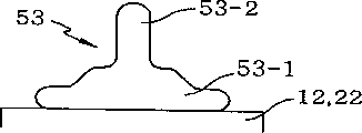
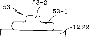
The stud bump 53 that forms by said method can have different shape.That is to say, as shown in figure 12, the 53-2 of long-neck portion that stud bump 53 can have body part 53-1 and form in the middle of body part 53-1.In addition, as shown in figure 13, stud bump 53 can have the short neck 53-2 that forms on body part 53-1.In addition, as shown in figure 14, stud bump 53 can be a convex shape, does not have projection in the centre of body part 53-1.Also have, as shown in figure 15, stud bump 53 can have trapezoidal body, does not have neck 53-2 in the centre of body part.In addition, as shown in figure 16, stud bump 53 can have very thick body part 53-1, and does not have neck 53-2.Owing in the forming process of stud bump, do not use harmful solder flux, thereby the stud bump forming process is an ecological, environmental protective, and simpler than welding method.
[formation of wedge shape projection and shape]
According to the method that on wafer 10 or substrate 21, forms wedge shape projection 63 of the present invention, as shown in figure 17, use the wedge bond instrument 65 of the line wherein inserted the gold thread 61 made by Al, Cu or Ag or high conductivity on pad 12 or 22, to form wedge shape projection 63.Particularly, after gold thread 61, aluminum steel 61-2 or copper cash 61-3 were inserted wedge bond instrument 65, the gold of fusing contacted with the pad of wafer 10 or substrate 21 in the wedge bond instrument 65.Subsequently, the gold that will melt by ultrasonic wave is bonded on the pad.Subsequently, wedge bond instrument 65 is mobile slightly on the direction of transverse axis, with bonding every line.Subsequently, every line is excised immediately.As a result, on wafer 10 or substrate 21, formed wedge shape projection 63.
The wedge shape projection 63 that forms by said method has different shape.That is to say, show the wedge shape projection 63 that has two projectioies, a projection and do not have projection as Figure 18 to 20 respectively.The shape of wedge shape projection 63 depends on the shape of various wedge tool.
[adhesive tape adhesion process]
Simultaneously, in the step S3 to pretreated wafer 10 adhesive tapes 72, under the situation of cutting the wafer 10 that is formed with stud bump on it, tube core (chip just) is fixed by adhesive tape, thereby tube core can not separate separately.Sectional elevation structure according to adhesive tape as shown in figure 21 when bonding, when adhesive tape 72 was supported by the frame loops 74 that is positioned at its two ends, wafer 10 was placed on the tacky surfaces of adhesive tape and is bonding with it subsequently.
[wafer cutting process]
In wafer cutting step S4, the chip of wafer state is cut device to be separated separately.According to cross sectional side view shown in Figure 22, even the blade 81 of cutter 80 has cut wafer 10 fully and part has been cut adhesive tape 72, chip 11 can or not separate separately because of adhesive tape 72 yet.
[engaging process]
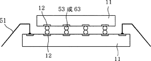
The schematic diagram of Figure 23 has illustrated the coupling device that adopts according to bonding flip chip of the present invention the time.This coupling device comprises clamping device (collet) 95 that is used to keep chip 11 and the piece (block) 100 that is used for support substrates 21.
With reference to Figure 23, for transmitting ultrasonic wave, keep the clamping device 95 of chip 11 on X-direction, to vibrate to chip, the piece 100 of support substrates 21 can vibrate on Y direction.In addition, clamping device 95 also can vibrate on Y direction, and piece 100 can vibrate on X-direction.In addition, clamping device 95 and piece 100 can transmit simultaneously same axially in the ultrasonic wave of intersection.Each method in the above-mentioned transfer approach can be used with only transmitting hyperacoustic conventional method from clamping device 95.Thereby, because ultrasonic wave can be sent to substrate 21 and chip 11,, and strengthened bonding strength between chip 11 and the substrate 21 so the flip-chip bond process can be finished in a short period of time.As a result, improved rate of finished products.
[definition of clamping device and surface treatment method]
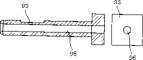
Herein, as Figure 24 and shown in Figure 25, owing to the central authorities that transmit the clamping device 95 of ultrasonic energy to chip have vacuum hole 96, it uses vacuum pressure supporting chip 11 also to transmit ultrasonic energy.
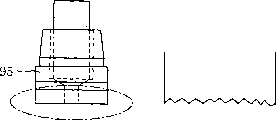
Above-mentioned clamping device 95 is divided into rough (matt) type clamping device that is used to polish the polishing type clamping device of contact surface and only coarse processing contact surface as shown in figure 27 as shown in figure 26.
In addition, clamping device utilizes anti-hyperacoustic material such as Zr, Ti, pottery, unoxidizable alloy, titanium alloy (for example TiW or TiC) etc. to make.
In addition, as shown in figure 28, can carry out the DLC coating to clamping device 95 and handle to prevent ultrasonic energy losses.Herein, by using on the surface of clamping device 95, grow carbon atom 9g and form diamond layer and make the DLC coating of spraying plating 99 or CVD (chemical vapour deposition (CVD)).If coated at the outer surface of clamping device and to be similar to adamantine carbon film 97, the external losses minimum of the ultrasonic energy that sends from transducer (transducer) then, and therefore, ultrasonic energy is sent to chip effectively.
[connected structure]
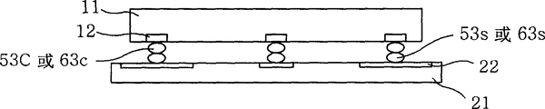
According to the method that forms projection on the pad 22 of substrate and bonding pads 12, when chip 11 was engaged on the pretreated substrate 21, the connected structure that is used for flip-chip bond of the present invention has different structures, and was as shown in table 1 below.
Table 1
| Embodiment (accompanying drawing) | Substrate condition | Chip status |
| Embodiment 1 (Figure 29) | Formed stud bump | Formed by the plating projection |
| Embodiment 2 (Figure 30) | There is not projection (bared) | Formed by the plating projection |
| Embodiment 3 (Figure 31) | Formed stud bump | Formed by plating projection and stud bump |
| Embodiment 4 (Figure 32) | There is not projection | Formed by plating projection and stud bump |
| Embodiment 5 (Figure 33) | Formed stud bump | Formed stud bump |
| Embodiment 6 (Figure 34) | Formed stud bump | Do not have the projection |
| Embodiment 7 (Figure 35) | Do not have the projection | Formed stud bump |
| Embodiment 8 (Figure 36) | There is not projection+adhesive (ACF, ACP, NCF or NCP) to use | Formed stud bump |
| Embodiment 9 (Figure 37) | There is not projection+adhesive (ACF, ACP, NCF or NCP) to use | Formed by the plating projection |
| Embodiment 10 (Figure 38) | Formed by the plating projection | Form or do not form by the plating projection |
Embodiment 1
Illustrating according to of the present invention of Figure 29 utilizes hot ultrasonic method at the substrate that is formed with stud bump with carry out the process of flip-chip bond between being formed with by the chip of plating projection.
With reference to Figure 29, the aluminum pad 12 of chip 11 have by Au, Al or scribble that the Ni of Au makes by the protruding 32c of plating.The lead pad 22 of substrate 21 has the stud bump 53S that is made by Au or Cu.In flip-chip bond process S5, after chip 11 and substrate 21 closely contacts, apply heat to substrate 21, and apply the ultrasonic wave of 70KHz or higher frequency by clamping device 95 to chip 11.Simultaneously, exert pressure to substrate 21.As a result, chip is bonded together by the energy that is produced by heat, ultrasonic wave and pressure by the stud bump 53s of protruding 32c of plating and substrate.Herein, the clamping device of being made up of Zr, Ti, pottery, stainless aluminium, TiW aluminium or TiC etc. 95 is manufactured with the size littler than each chip.
Embodiment 2
The process that illustrates the hot ultrasonic method of use according to the present invention bonding flip chip and between being formed with by the chip of plating projection of Figure 30 at the substrate that does not have projection (bared).
With reference to Figure 30, the aluminum pad 12 of chip 11 have by Au, Al or scribble that the Ni of Au makes by the protruding 32c of plating.The lead pad 22 of substrate 21 is without any projection.In flip-chip bond process S5, after chip 11 and substrate 21 closely contacts, apply heat to substrate 21, and apply ultrasonic wave to chip 11 by clamping device 95.Simultaneously, exert pressure to substrate 21.As a result, chip is bonded together by the energy that is produced by heat, ultrasonic wave and pressure by protruding 32c of plating and substrate lead pad 22.
Embodiment 3
Figure 31 illustrates the hot ultrasonic method of use according to the present invention at the substrate that is formed with stud bump with have a process that is formed on by bonding flip chip between the chip of the stud bump of plating on the projection.
With reference to Figure 31, the aluminum pad 12 of chip 11 have by Au, Al or scribble that the Ni of Au makes by the protruding 32c of plating, plated and be formed with stud bump 53c on the protruding 32c.The lead pad 22 of substrate 21 has stud bump 53s.In flip-chip bond process S5, after chip 11 and substrate 21 closely contacts, apply heat to substrate 21, and the ultrasonic wave of 70KHz or higher frequency is provided to chip 11 by clamping device 95.Simultaneously, exert pressure to substrate 21.As a result, chip is bonded together by the energy that ultrasonic wave and pressure by heat, 70KHz or higher frequency produce by the stud bump 53s of protruding 53c of plating and substrate.
Embodiment 4
Figure 32 illustrates the hot ultrasonic method of use according to the present invention at substrate with have by plating projection and be formed on the process of bonding flip chip between this chip that is plated the stud bump on the projection.
With reference to Figure 32, the aluminum pad 12 of chip 11 have by Au, Al or scribble that the Ni of Au makes by the protruding 32c of plating, on by the protruding 32c of plating, formed stud bump 53c.The lead pad 22 of substrate 21 does not have any projection.In flip-chip bond process S5, after chip 11 and substrate 21 closely contacts, apply heat to substrate 21, and provide ultrasonic wave to chip 11 by clamping device 95.Simultaneously, exert pressure to substrate 21.As a result, the lead pad 22 of the stud bump 53c of chip and substrate is bonded together by the energy that ultrasonic wave and pressure by heat, 70KHz or higher frequency produce.
Embodiment 5
Figure 33 illustrates the hot ultrasonic method of use according to the present invention at the substrate that has stud bump 53s with have the process of bonding flip chip between the chip of stud bump 53c.
With reference to Figure 33, the aluminum pad 12 of chip 11 has the stud bump 53c that is made by Au or Cu.The lead pad 22 of substrate 21 has the stud bump 53S that is made by Au or Cu.In flip-chip bond process S5, after chip 11 and substrate 21 closely contacts, apply heat to substrate 21, and apply ultrasonic wave to chip 11 by clamping device 95.Simultaneously, exert pressure to substrate 21.As a result, the stud bump 53s of the stud bump 53c of chip and substrate is bonded together by the energy that is produced by heat, ultrasonic wave and pressure.
Embodiment 6
Figure 34 illustrates the hot ultrasonic method of use according to the present invention at the substrate that has stud bump 53s with have the process of bonding flip chip between the chip of basic aluminum pad.
With reference to Figure 34, the aluminum pad 12 of chip 11 does not have any projection.The lead pad 22 of substrate 21 has the stud bump 53S that is made by Au or Cu.In flip-chip bond process S5, after chip 11 and substrate 21 closely contacted, apply heat to substrate 21, and apply ultrasonic wave to chip 11 by clamping device 95.Simultaneously, exert pressure to substrate 21.As a result, the stud bump 53s of bonding pads 12 and substrate is bonded together by the energy that is produced by heat, ultrasonic wave and pressure.
Embodiment 7
Figure 35 illustrates the hot ultrasonic method of use according to the present invention in base substrate with have the process of bonding flip chip between the chip of stud bump 53c.
With reference to Figure 35, the aluminum pad 12 of chip 11 has the stud bump 53c that is made by Au or Cu.The lead pad 22 of substrate 21 does not have any protruding 53S.In flip-chip bond process S5, after chip 11 and substrate 21 closely contacts, apply heat to substrate 21, and apply ultrasonic wave to chip 11 by clamping device 95.Simultaneously, exert pressure to substrate 21.As a result, the lead pad 22 of the stud bump 53c of chip and substrate 21 is bonded together by the energy that is produced by heat, ultrasonic wave and pressure.
Figure 36 illustrates the hot ultrasonic method of use according to the present invention in the base substrate that has applied adhesive (for example ACF, ACP, NCF or NCP) with have the process of bonding flip chip between the chip of stud bump 53c.
With reference to Figure 36, the aluminum pad 12 of chip 11 has the stud bump 53c that is made by Au or Cu.The lead pad 22 of substrate 21 does not have any projection.On the lead pad 22 of substrate 21, apply the adhesive 102 that is selected from anisotropic conducting film (ACF), anisotropic conductive cream (ACP), non-conductive film (NCF) and non-conductive cream (NCP).In flip-chip bond process S5, after chip 11 and substrate 21 closely contacts, apply heat to substrate 21, and apply ultrasonic wave to chip 11 by clamping device 95.Simultaneously, exert pressure to substrate 21.As a result, the lead pad 22 of the stud bump 53c of chip and substrate 21 is bonded together by the energy that is produced by heat, ultrasonic wave and pressure.
Embodiment 9
The process that illustrates the hot ultrasonic method of use according to the present invention bonding flip chip and between having by the chip of plating projection of Figure 37 at the substrate that has applied adhesive (for example ACF, ACP, NCF or NCP).
With reference to Figure 37, the aluminum pad 12 of chip 11 have by Au, Al or scribble that the Ni of Au makes by the protruding 32c of plating.The lead pad 22 of substrate 21 does not have any projection.On the lead pad 22 of substrate 21, apply the adhesive 102 that is selected from ACF, ACP, NCF and NCP.In flip-chip bond process S5, after chip 11 and substrate 21 closely contacted, apply heat to substrate 21, and apply ultrasonic wave to chip 11 by clamping device 95.Simultaneously, exert pressure to substrate 21.As a result, the lead pad 22 by protruding 32c of plating and substrate 21 of chip is bonded together by the energy that is produced by heat, ultrasonic wave and pressure.
By the narration of front as can be known, the projection that is formed on substrate 21 and the chip 11 according to the present invention comprise the stud bump of making by the plating projection, by the Ni that scribbles Au of making by the plating projection, by Au made by Au, Al, the stud bump made by Cu or the like.In addition, substrate 21 can be conventional PCB or FPCB.In addition, substrate 21 can be the substrate that is coated with Sn on it.For realizing having the flip-chip process of better bonding force, on substrate, apply ACF, ACP, NCF or NCP.
With reference to Figure 38, the aluminum pad 12 of chip 11 can have by Au, Al or scribble that the Ni of Au makes by the protruding 32c of plating.In addition, chip 11 can only not have the aluminum pad 12 that forms the protruding 32c of quilt plating.Substrate 21 can have the projection 43 of mixing.Utilize ultrasonic energy that chip 11 and substrate 21 are engaged.
By aforementioned content as can be known, the engagement means according in flip-chip bond process S5 of the present invention applies heat to substrate 21, and applies ultrasonic wave by clamping device 95 to chip 11.And exert pressure to substrate 21.As a result, chip 11 and substrate 21 are bonded together by the energy that is produced by heat, ultrasonic wave and pressure.Thereby, the invention has the advantages that because the present invention has adopted the method that applies ultrasonic wave and hot pressing, rather than only use the hot-press method of routine, thereby compare with routine techniques, it has reduced the processing time.In addition, at the substrate that uses plating Sn or applied on it under situation of substrate of ACF, ACP, NCF or NCP, can obtain more outstanding bonding force.
[remodeling]
Figure 39 shows according to the embodiment of the connected structure of the relative size of stud bump or wedge shape projection and apply the embodiment of ACF, ACP, NCF or NCP after forming projection to Figure 42.
Particularly, in Figure 39, the protruding 53c of chip 11 or 63c are bigger than the protruding 53s or the 63s of substrate 21.In addition, in Figure 40, protruding 53c or 63c are the same big with the protruding 53s or the 63s of substrate 21.In addition, in Figure 41, the protruding 53s of substrate or 63s are bigger than the protruding 53c or the 63c of chip.From the narration of front, as can be known, have identical size and type or have the protruding 53c of chip of different sizes and type or the protruding 53s or the 63s of 63c and substrate can be joined together.
In Figure 42, on substrate 21, form after protruding 54s or the 63s, apply anisotropic-electroconductive adhesive 102 or non-conductive adhesive 102 such as ACF, ACP, NCF or NCP etc.Subsequently, chip 11 and substrate 21 engage rapidly.Thereby, can remove the process of potting resin.Can around the projection that is formed on the substrate 21, apply anisotropic-electroconductive adhesive 102 or non-conductive adhesive 102 such as ACF, ACP, NCF or NCP.In addition, can on entire substrate 21, apply.
[chip-stacked]
With reference to Figure 43, forming stud bump 53 or wedge shape projection 63 on the pad 12 of last chip 11 or on the pad 12 of following chip 11.Herein, following bonding pads 12 has two row at least.The pad of two chips 11 in location is faced them mutually.Downwards chip 11 applies heat, by clamping device 95 upwards chip 11 apply ultrasonic wave and pressure.As a result, last chip 11 and following chip 11 are engaged the chip that piles up with formation.This chip that piles up presents than single chip more performance.
Figure 44 illustrates by form stud bump 53 or wedge shape projection 63 on last chip, forming stud bump 53 or wedge shape projection 63 on the chip 11 down, they are faced mutually, and tool using applies ultrasonic wave and pressure is made according to stacked chips of the present invention then.
Figure 45 illustrates by forming on last chip 11 by plating projection 32, forming stud bump 53 or wedge shape projection 63 on the chip 11 down, engages them then and makes according to stacked chips of the present invention.
[reprocessing]
After flip-chip bond process S5, in last handling process, if desired, potting resin is protected chip between the joint space.Figure 47 shows and forms protective bulkhead 132, forms protruding 53c, 53s and 63 and form the embodiment of mold (molding) 134 on them respectively on chip 11 and substrate 21.Particularly, in the preprocessing process,, finish flip-chip bond in the reprocessing that is used for filling (under-fill) down and side seal then, can prevent that so epoxy resin from infiltrating the slit between projection and the substrate if around chip, form protective bulkhead 132.Herein, protective bulkhead 132 can be made up of NCP, NCF, ACF, ACP, epoxy resin or mouldable compound.After finishing the flip-chip bond process, preferably, the remedial procedures of the protective bulkhead 132 that increasing is used to harden is made by soft material.
[stepped construction of substrate]
Simultaneously, stepped construction according to the substrate that is used to engage of the present invention comprises: the hard metal level that has the substrate of copper patterning thin film on the base material, forms by the metal that plates high rigidity on substrate, the conductive metal layer that forms by the metal that plates high conductivity on hard metal level.Thereby bond strength is kept, and rate of finished products is enhanced, and is not subjected to the influence of base material kind.
Figure 48 shows the metal laminate structure that is used for the substrate of stud bump according to of the present invention.With reference to Figure 48, substrate 21 according to the present invention is formed with the copper patterning thin film on its base material.Herein, the base material of substrate is made up of FPCB, FR4, FR5, pottery or glass.
Method by plating forms the first metal layer 141 and second metal level 142 on substrate 21.The first metal layer 141 is as the resilient coating of the base material kind effect of blocking-up substrate.It is by plating 3 μ m or thicker Pd alloy, Pd-Ni or Ni-Pd formation.Second metal level at engaging process as the part that is directly connected to stud bump etc.It is by plating 0.1 μ m or the thicker Au with satisfactory electrical conductivity and purity or Ag, Au/Ag, Al, Au alloy, Ag alloy or the formation of Al alloy.
Thereby, owing to increased the hard metal buffer layer 141 of the effect that is used to block the substrate kind, thereby no matter the kind of base material how, all can keep bond strength and improve rate of finished products.
Figure 49 shows has three layers stepped construction, and it is as another embodiment that is used for each protruding metal laminate structure according to the present invention.
With reference to Figure 49, substrate 21 according to the present invention is formed with the copper patterning thin film on its base material.Herein, the base material of substrate is made by FPCB, FR4, FR5, pottery or glass.
Method by plating forms the first metal layer 151, second metal level 152 and the 3rd metal level 153 on substrate 21.
By plating 3 μ m or thicker Ni or Ni alloy formation the first metal layer 151.Second metal level 152 is as the effect of resilient coating with the material category that is used for blocking substrate, and it is by plating 0.1 μ m or thicker AU alloy forms.
The 3rd metal level 153 at engaging process as the part that is directly connected to each projection etc.Its use has Au or Ag, Al, Au alloy, Ag alloy or the Al alloy of satisfactory electrical conductivity and purity.
Like this owing to increased the hard metal buffer layer of the effect that is used to stop the substrate kind, thereby no matter the kind of base material how, all can keep bond strength and improve rate of finished products.
Commercial Application
As can be known, according to the present invention, owing in the flip-chip bond process, ultrasonic wave applies with hot pressing, thereby this process can be finished rapidly from the narration of front.Especially by on chip, forming stud bump or, on substrate, forming projection, and directly engage these projectioies, can greatly strengthen the zygosity of chip by the plating projection.That is to say that directly connect by plating projection, stud bump, wedge shape projection or the projection of mixing by using clamping device, and form new intermetallic zone behind joint, the present invention can strengthen zygosity.Further, because substrate is coated with the fusing point Al lower than Au, Cu or Sn, thereby, the electric reliability of easier assurance, and bonding force is higher.Therefore, even if use and to have fragile pad the wafer of (as imageing sensor etc.), also can nondestructively realize flip-chip bond.
Further, the invention provides a kind of flip-chip device, it only applies the ultrasonic energy that is used for flip-chip bond to chip or to chip and substrate.
Further, according to the present invention,, increase rate of finished products because the metal of high rigidity is plated on the substrate base material kind effect with the blocking-up substrate as resilient coating, thereby can keep bond strength.
Though the preferred embodiments of the present invention have more than been described, should be clear, concerning those skilled in the art, under the situation that does not break away from spirit of the present invention, various improvement and variation all are conspicuous.Thereby scope of the present invention only is indicated in the appended claims.
Claims (22)
1. flip chip bonding method is used for having semiconductor package process on the substrate of lead pad in the chip join that will have pad and strengthens and engage performance, said method comprising the steps of:
Wafer with chip is carried out preliminary treatment, described wafer is cut, and obtain through pretreated single chip;
Substrate is carried out preliminary treatment;
Make through the pad alignment of pretreated described bonding pads, apply ultrasonic wave and heat by using clamping device, and exert pressure simultaneously, described chip and described substrate are bonded together with the pretreated described substrate of process; And
Carrying out reprocessing fills or casting with the resin after engaging.
2. method according to claim 1 is characterized in that, the described lead pad of described substrate is plated with Au, Sn or high-conductivity metal.
3. method according to claim 1, it is characterized in that the pre-treatment step of described substrate is selected from any one in the following process: under the state that does not have projection by, form by the plating projection, form stud bump, form and mix projection and apply adhesive.
4. method according to claim 3 is characterized in that, it is one of following that described adhesive is selected from: anisotropic conducting film, anisotropic conductive cream, non-conductive film and non-conductive cream.
5. method according to claim 1, it is characterized in that the pre-treatment step of described wafer is selected from any one in the following process: under the state that does not have projection by, form by the plating projection, form stud bump after forming stud bump or wedge shape projection and forming by the plating projection.
6. according to claim 3 or 5 described methods, it is characterized in that, described by plating projection by be selected from Au, Al and scribble among the Ni of Au any one make, and described stud bump is made by in the high-conductivity metal that is selected from Au, Ag, Al and Cu any one.
7. according to claim 3 or 5 described methods, it is characterized in that the described projection of being plated provides the size of annealing effect with increase Au particle, thereby improves described by the bonding force of plating projection.
8. according to claim 3 or 5 described methods, it is characterized in that, the projection of described substrate has identical size with the projection of described chip, and perhaps any in the projection of the projection of described substrate and described chip has bigger size than in them another.
9. according to claim 3 or 5 described methods, it is characterized in that the projection that forms has and is selected from one of following shape: long convex shaped, short convex shaped and the convex that does not have projection on described wafer or described substrate.
10. method according to claim 1 is characterized in that, the described clamping device that is used to support described chip and transmits ultrasonic energy is made by being selected from one of following material: Zr, Ti, pottery, unoxidizable alloy, TiW and TiC.
11. method according to claim 10 is characterized in that, described clamping device utilization is similar to adamantine carbon film and is subjected to DLC coating processing, so that the loss of described ultrasonic energy reaches minimum.
12. method according to claim 10, it is characterized in that, described clamping device adopts the polishing type clamping device of bottom surface of the described clamping device of polishing or the rough type clamping device that carries out coarse processing by sand milling or edm and to its surface, thereby makes the ultrasonic energy maximum of transmission.
13. method according to claim 1 is characterized in that, described ultrasonic wave is used in the safety frequency scope, and wherein said safe range is that 50KHz is to 100KHz; Perhaps described ultrasonic wave is used in the scope that can reduce the ultrasonic energy loss, and wherein said scope is that 100KHz is to 250KHz.
14. method according to claim 1, it is characterized in that, the step of utilizing described ultrasonic wave to engage described flip-chip is to utilize the flip-chip bond device have clamping device and the piece that supports described substrate to realize, and describedly applies hyperacoustic step and be selected from the following process any one: transmit ultrasonic wave and the ultrasonic wave from described block movement along Y direction along X-direction from described clamping device, ultrasonic wave and ultrasonic wave from described clamping device transmission along Y direction from described block movement along X-direction, and from described clamping device and described block movement same axially the ultrasonic wave of intersection.
15. method according to claim 14, it is characterized in that, describedly apply hyperacoustic step and be selected from the following process any one: from described clamping device apply 50KHz in the 100KHz scope ultrasonic wave and from described apply the ultrasonic wave of 100KHz in the 250KHz scope, from described clamping device apply 100KHz in the 250KHz scope ultrasonic wave and from described apply 70KHz in the 100KHz scope ultrasonic wave and apply the ultrasonic wave that is in the same frequency range from described clamping device and described.
16. a method that is used to make the flip-chip that piles up, its can with go up chip join on following chip to obtain the high-performance in the unit are, said method comprising the steps of:
On the chip of wafer, form by in plating projection, stud bump and the wedge shape projection any one, cut described wafer, and prepare any one the single chip of going up that is formed with by in plating projection, stud bump and the wedge shape projection;
Prepare the following chip that does not have projection; And
Described described by in plating projection, stud bump and the wedge shape projection any one of going up chip aimed at described bonding pads down, and by applying that ultrasonic wave and heat are also exerted pressure simultaneously so that described upward chip with described under chip join be in the same place.
17. a method that is used to make the flip-chip that piles up, its can with go up chip join on following chip to obtain the high-performance in the unit are, said method comprising the steps of:
On the chip of wafer, form by in plating projection, stud bump and the wedge shape projection any one, cut described wafer, and prepare any one the single chip of going up that is formed with by in plating projection, stud bump and the wedge shape projection;
One chip join is formed stud bump or wedge shape projection to the substrate that has tackifying resin series, on described bonding pads, and prepare described chip down; And
Described described by in plating projection, stud bump and the wedge shape projection any one of going up chip aimed at the stud bump or the wedge shape projection of described chip down, and by applying that ultrasonic wave and heat are also exerted pressure simultaneously so that described upward chip with described under chip join be in the same place.
18. a metal laminate structure that is used for the substrate of bonding flip chip, described structure comprises:
Substrate, it is formed with the composition of copper film on base material;
Hard metal level, it forms by the metal that plates high rigidity on described substrate; And
Conductive metal layer, it forms by the metal that plates high conductivity on described hard metal level;
Thus, no matter the kind of described base material how, can both be kept bond strength and improve rate of finished products.
19. structure according to claim 18 is characterized in that, described structure also comprises a metal level, and described metal level is formed between described substrate and the described hard metal level, and described metal level is made by Ni or Ni alloy.
20., it is characterized in that described transmission metal level forms by in Au, Ag, Au/Ag, Al, Au alloy, Ag alloy and the Al alloy any one of being selected from that plates 0.1 μ m or bigger thickness according to claim 18 or 19 described structures.
21. according to claim 18 or 19 described structures, it is characterized in that described hard metal level forms by any one that is selected from the following process: plate 1 μ m or thicker Ni or Ni alloy, plate 0.1 μ m or thicker Pd alloy or Pd-Ni or Ni-Pd, plate 0.1 μ m or thicker Au and plate 0.1 μ m or thicker Au or Ag alloy.
22., it is characterized in that the base material of described substrate is made by being selected from the following material any one: FPCB, FR4, FR5, pottery and glass according to claim 18 or 19 described structures.
Applications Claiming Priority (2)
| Application Number | Priority Date | Filing Date | Title |
|---|---|---|---|
| KR1020030083891 | 2003-11-25 | ||
| KR20030083891 | 2003-11-25 |
Publications (1)
| Publication Number | Publication Date |
|---|---|
| CN1622304A true CN1622304A (en) | 2005-06-01 |
Family
ID=34588038
Family Applications (1)
| Application Number | Title | Priority Date | Filing Date |
|---|---|---|---|
| CNA2004100803660A Pending CN1622304A (en) | 2003-11-25 | 2004-09-29 | Flip chip bonding method and layered metal architecture of substrate for stud bump |
Country Status (7)
| Country | Link |
|---|---|
| US (1) | US7115446B2 (en) |
| JP (1) | JP2005159356A (en) |
| KR (1) | KR100604334B1 (en) |
| CN (1) | CN1622304A (en) |
| SG (1) | SG128468A1 (en) |
| TW (1) | TWI255019B (en) |
| WO (1) | WO2005053013A1 (en) |
Cited By (3)
| Publication number | Priority date | Publication date | Assignee | Title |
|---|---|---|---|---|
| US7429796B2 (en) | 2006-03-27 | 2008-09-30 | Fujitsu Limited | Semiconductor device and fabrication process thereof |
| CN101904230A (en) * | 2007-12-18 | 2010-12-01 | 美光科技公司 | Methods of fluxless micro-piercing of solder balls, and resulting devices |
| CN101331681B (en) * | 2005-12-21 | 2012-04-18 | 株式会社大真空 | Piezoelectric vibration piece and piezoelectric vibration device |
Families Citing this family (46)
| Publication number | Priority date | Publication date | Assignee | Title |
|---|---|---|---|---|
| US7142909B2 (en) * | 2002-04-11 | 2006-11-28 | Second Sight Medical Products, Inc. | Biocompatible bonding method and electronics package suitable for implantation |
| US20060211233A1 (en) * | 2005-03-21 | 2006-09-21 | Skyworks Solutions, Inc. | Method for fabricating a wafer level package having through wafer vias for external package connectivity and related structure |
| US7576426B2 (en) * | 2005-04-01 | 2009-08-18 | Skyworks Solutions, Inc. | Wafer level package including a device wafer integrated with a passive component |
| US7348212B2 (en) * | 2005-09-13 | 2008-03-25 | Philips Lumileds Lighting Company Llc | Interconnects for semiconductor light emitting devices |
| WO2006134220A1 (en) * | 2005-06-16 | 2006-12-21 | Imbera Electronics Oy | Method for manufacturing a circuit board structure, and a circuit board structure |
| JP4768343B2 (en) * | 2005-07-27 | 2011-09-07 | 株式会社デンソー | Mounting method of semiconductor element |
| JP4728782B2 (en) * | 2005-11-15 | 2011-07-20 | パナソニック株式会社 | Semiconductor device and manufacturing method thereof |
| US7408243B2 (en) * | 2005-12-14 | 2008-08-05 | Honeywell International Inc. | High temperature package flip-chip bonding to ceramic |
| US20070141749A1 (en) * | 2005-12-20 | 2007-06-21 | Yi-Fong Lin | Die attachment method for LED chip and structure thereof |
| US20070222087A1 (en) * | 2006-03-27 | 2007-09-27 | Sangdo Lee | Semiconductor device with solderable loop contacts |
| KR100762909B1 (en) * | 2006-08-31 | 2007-10-08 | 주식회사 하이닉스반도체 | Manufacturing process of flip chip package |
| US8258625B2 (en) * | 2007-04-06 | 2012-09-04 | Hitachi, Ltd. | Semiconductor device |
| US20090014852A1 (en) * | 2007-07-11 | 2009-01-15 | Hsin-Hui Lee | Flip-Chip Packaging with Stud Bumps |
| KR100896127B1 (en) * | 2007-07-20 | 2009-05-07 | 성균관대학교산학협력단 | Plated bumps coated with tin and flip chip bonding method using them |
| TWI362525B (en) * | 2007-07-31 | 2012-04-21 | Chunghwa Picture Tubes Ltd | Active device array substrate and liquid crystal display panel |
| US8283756B2 (en) * | 2007-08-20 | 2012-10-09 | Infineon Technologies Ag | Electronic component with buffer layer |
| KR20150068495A (en) | 2007-11-30 | 2015-06-19 | 스카이워크스 솔루션즈, 인코포레이티드 | Wafer level packaging using flip chip mounting |
| US7642135B2 (en) * | 2007-12-17 | 2010-01-05 | Skyworks Solutions, Inc. | Thermal mechanical flip chip die bonding |
| US8900931B2 (en) * | 2007-12-26 | 2014-12-02 | Skyworks Solutions, Inc. | In-situ cavity integrated circuit package |
| US8018075B2 (en) * | 2008-07-11 | 2011-09-13 | Advanced Semiconductor Engineering, Inc. | Semiconductor package, method for enhancing the bond of a bonding wire, and method for manufacturing a semiconductor package |
| DE102008040614A1 (en) | 2008-07-22 | 2010-01-28 | Robert Bosch Gmbh | Contacting method for substrate-based circuits and associated circuitry |
| KR100958513B1 (en) | 2008-07-31 | 2010-05-17 | 알티전자 주식회사 | Electrode pad and light emitting diode package including the same |
| EP2340559A1 (en) * | 2008-09-16 | 2011-07-06 | Agere Systems, Inc. | Pb-free solder bumps with improved mechanical properties |
| KR20100053016A (en) * | 2008-11-12 | 2010-05-20 | 한국과학기술원 | (method for bonding between electrical devices by adjusting the heating temperature of adhesive and apparatus for bonding between electrical devices by adjusting the heating temperature of adhesive |
| TWI404198B (en) * | 2009-04-22 | 2013-08-01 | Ind Tech Res Inst | Sensor package structure and method thereof |
| US8476757B2 (en) * | 2009-10-02 | 2013-07-02 | Northrop Grumman Systems Corporation | Flip chip interconnect method and design for GaAs MMIC applications |
| JP2011151322A (en) * | 2010-01-25 | 2011-08-04 | Japan Aviation Electronics Industry Ltd | Flip-chip mounting structure and flip-chip mounting method |
| TWI411075B (en) * | 2010-03-22 | 2013-10-01 | Advanced Semiconductor Eng | Semiconductor package and manufacturing method thereof |
| US9406658B2 (en) | 2010-12-17 | 2016-08-02 | Advanced Semiconductor Engineering, Inc. | Embedded component device and manufacturing methods thereof |
| TW201243930A (en) * | 2011-04-21 | 2012-11-01 | Lingsen Precision Ind Ltd | Wafer dicing method |
| US20130087915A1 (en) * | 2011-10-10 | 2013-04-11 | Conexant Systems, Inc. | Copper Stud Bump Wafer Level Package |
| US8618795B1 (en) * | 2012-06-29 | 2013-12-31 | General Electric Company | Sensor assembly for use in medical position and orientation tracking |
| US8890274B2 (en) | 2012-07-11 | 2014-11-18 | Taiwan Semiconductor Manufacturing Company, Ltd. | Interconnect structure for CIS flip-chip bonding and methods for forming the same |
| KR102233334B1 (en) | 2014-04-28 | 2021-03-29 | 삼성전자주식회사 | Tin plating solution, Tin plating equipment and method for fabricating semiconductor device using the tin plating solution |
| US9209147B1 (en) | 2014-07-17 | 2015-12-08 | Freescale Semiconductor, Inc. | Method of forming pillar bump |
| KR102380834B1 (en) | 2015-01-06 | 2022-03-31 | 삼성전기주식회사 | Printed circuit board, semiconductor package and method of manufacturing the same |
| CN104576973B (en) * | 2015-01-30 | 2017-04-05 | 京东方科技集团股份有限公司 | The flattening method and system, method for packing on the fluid sealant surface of encapsulation cover plate |
| KR20160095520A (en) | 2015-02-03 | 2016-08-11 | 삼성전기주식회사 | Printed circuit board, semiconductor package and method of manufacturing the same |
| US9683278B2 (en) | 2015-06-08 | 2017-06-20 | Infineon Technologies Ag | Diffusion solder bonding using solder preforms |
| JP2016001752A (en) * | 2015-08-25 | 2016-01-07 | 日本航空電子工業株式会社 | Flip-chip mounting structure and flip-chip mounting method, and using method of flip-chip mounting structure |
| US10147702B2 (en) * | 2016-10-24 | 2018-12-04 | Palo Alto Research Center Incorporated | Method for simultaneously bonding multiple chips of different heights on flexible substrates using anisotropic conductive film or paste |
| KR101880102B1 (en) * | 2017-05-30 | 2018-07-20 | 제엠제코(주) | Stacked semiconductor package |
| US11495524B2 (en) * | 2018-06-12 | 2022-11-08 | Texas Instruments Incorporated | QFN device having a mechanism that enables an inspectable solder joint when attached to a PWB and method of making same |
| US11862587B2 (en) * | 2019-07-25 | 2024-01-02 | Advanced Semiconductor Engineering, Inc. | Semiconductor package structure and method of manufacturing the same |
| JP7257296B2 (en) * | 2019-09-06 | 2023-04-13 | ファスフォードテクノロジ株式会社 | Die bonding apparatus and semiconductor device manufacturing method |
| CN111009481B (en) * | 2019-12-19 | 2023-04-18 | 西北电子装备技术研究所(中国电子科技集团公司第二研究所) | Chip substrate high-pressure flip-chip bonding flexible pressurization method |
Family Cites Families (16)
| Publication number | Priority date | Publication date | Assignee | Title |
|---|---|---|---|---|
| JPH07115109A (en) * | 1993-10-15 | 1995-05-02 | Nec Corp | Flip chip bonding method and device thereof |
| US5503286A (en) * | 1994-06-28 | 1996-04-02 | International Business Machines Corporation | Electroplated solder terminal |
| JP3243956B2 (en) * | 1995-02-03 | 2002-01-07 | 松下電器産業株式会社 | Semiconductor device and manufacturing method thereof |
| JPH1012669A (en) * | 1996-06-21 | 1998-01-16 | Toshiba Corp | Connection of flip chip |
| JPH10209218A (en) * | 1997-01-24 | 1998-08-07 | Rohm Co Ltd | Production of semiconductor chip having anisotropic conductive film and its mounting method |
| JP3923248B2 (en) * | 1996-12-27 | 2007-05-30 | 松下電器産業株式会社 | Method of mounting electronic component on circuit board and circuit board |
| US5950070A (en) * | 1997-05-15 | 1999-09-07 | Kulicke & Soffa Investments | Method of forming a chip scale package, and a tool used in forming the chip scale package |
| JPH11284028A (en) * | 1998-03-27 | 1999-10-15 | Toshiba Corp | Bonding method and its device |
| KR20000002962A (en) * | 1998-06-24 | 2000-01-15 | 윤종용 | Chip scale package of wafer level and manufacturing method thereof |
| JP3661444B2 (en) * | 1998-10-28 | 2005-06-15 | 株式会社ルネサステクノロジ | Semiconductor device, semiconductor wafer, semiconductor module, and semiconductor device manufacturing method |
| JP3504543B2 (en) * | 1999-03-03 | 2004-03-08 | 株式会社日立製作所 | Semiconductor device separation method and device, and semiconductor device mounting method |
| JP3503133B2 (en) * | 1999-12-10 | 2004-03-02 | 日本電気株式会社 | Connection method of electronic device assembly and electronic device |
| JP2002151551A (en) * | 2000-11-10 | 2002-05-24 | Hitachi Ltd | Flip-chip mounting structure, semiconductor device therewith and mounting method |
| JP3609737B2 (en) * | 2001-03-22 | 2005-01-12 | 三洋電機株式会社 | Circuit device manufacturing method |
| JP2003197672A (en) * | 2001-12-25 | 2003-07-11 | Nec Electronics Corp | Method of manufacturing semiconductor device |
| KR100544274B1 (en) * | 2003-06-25 | 2006-01-24 | (주)케이나인 | Layered metal architecture of substrate for stud bump |
-
2004
- 2004-05-28 KR KR1020040038214A patent/KR100604334B1/en not_active IP Right Cessation
- 2004-08-04 WO PCT/KR2004/001956 patent/WO2005053013A1/en active Application Filing
- 2004-09-02 SG SG200404949A patent/SG128468A1/en unknown
- 2004-09-21 TW TW093128559A patent/TWI255019B/en not_active IP Right Cessation
- 2004-09-29 CN CNA2004100803660A patent/CN1622304A/en active Pending
- 2004-10-13 US US10/964,371 patent/US7115446B2/en not_active Expired - Fee Related
- 2004-11-19 JP JP2004336518A patent/JP2005159356A/en active Pending
Cited By (7)
| Publication number | Priority date | Publication date | Assignee | Title |
|---|---|---|---|---|
| CN101331681B (en) * | 2005-12-21 | 2012-04-18 | 株式会社大真空 | Piezoelectric vibration piece and piezoelectric vibration device |
| US7429796B2 (en) | 2006-03-27 | 2008-09-30 | Fujitsu Limited | Semiconductor device and fabrication process thereof |
| US7754536B2 (en) | 2006-03-27 | 2010-07-13 | Fujitsu Limited | Semiconductor device and fabrication process thereof |
| CN101904230A (en) * | 2007-12-18 | 2010-12-01 | 美光科技公司 | Methods of fluxless micro-piercing of solder balls, and resulting devices |
| US8669173B2 (en) | 2007-12-18 | 2014-03-11 | Micron Technology | Methods of fluxless micro-piercing of solder balls, and resulting devices |
| US10163840B2 (en) | 2007-12-18 | 2018-12-25 | Micron Technology, Inc. | Methods of fluxless micro-piercing of solder balls, and resulting devices |
| US10515918B2 (en) | 2007-12-18 | 2019-12-24 | Micron Technology, Inc. | Methods of fluxless micro-piercing of solder balls, and resulting devices |
Also Published As
| Publication number | Publication date |
|---|---|
| TW200520175A (en) | 2005-06-16 |
| SG128468A1 (en) | 2007-01-30 |
| WO2005053013A1 (en) | 2005-06-09 |
| KR100604334B1 (en) | 2006-08-08 |
| US20050110163A1 (en) | 2005-05-26 |
| US7115446B2 (en) | 2006-10-03 |
| JP2005159356A (en) | 2005-06-16 |
| TWI255019B (en) | 2006-05-11 |
| KR20050050155A (en) | 2005-05-30 |
Similar Documents
| Publication | Publication Date | Title |
|---|---|---|
| CN1622304A (en) | Flip chip bonding method and layered metal architecture of substrate for stud bump | |
| CN1300180A (en) | Chip mounting, circuit board, data carrier and mfg. method thereof and electronic element assembly | |
| CN1076872C (en) | Chip carrier and method of manufacturing and mounting the same | |
| CN1226786C (en) | Lead wire holder | |
| CN1214458C (en) | RF module member including surface elastic wave element and its manufacture method | |
| US7642135B2 (en) | Thermal mechanical flip chip die bonding | |
| CN1491439A (en) | Multi-chip circuit module and method for producing the same | |
| CN1790651A (en) | Manufacturing method of chip integrated substrate | |
| CN1280884C (en) | Semiconductor device and manufacture thereof, circuit board and electronic machine | |
| CN1270363C (en) | Manufacturing method for electronic component module and electromagnetically readable data carrier | |
| CN1649162A (en) | Optical sensor module | |
| CN101047146A (en) | Method of manufacturing semiconductor device | |
| CN1976015A (en) | Semiconductor device and method for manufacturing same, and semiconductor wafer | |
| CN1437256A (en) | Semiconductor element and producing method thereof, and semiconductor device and producing method thereof | |
| CN1777988A (en) | Taped lead frames and methods of making and using the same in semiconductor packaging | |
| JP2014503936A (en) | Sintered material and mounting method using the same | |
| CN1606143A (en) | Semiconductor element mounting method and mounting substrate | |
| CN1309425A (en) | Semiconductor integrated circuit device and mfg. method thereof | |
| CN1763941A (en) | Semiconductor device having aluminum electrode and metallic electrode | |
| CN1512580A (en) | Semiconductor device and its producing method | |
| CN1949468A (en) | Method for interconnecting and packaging 3-D multi-chip module | |
| CN101047155A (en) | Semiconductor device and manufacturing method thereof | |
| CN1825578A (en) | Semiconductor device manufacturing method | |
| CN1427471A (en) | Semiconductor device | |
| JP2009283484A (en) | Semiconductor device, method for mounting semiconductor device, and mounting structure of semiconductor device |
Legal Events
| Date | Code | Title | Description |
|---|---|---|---|
| C06 | Publication | ||
| PB01 | Publication | ||
| C10 | Entry into substantive examination | ||
| SE01 | Entry into force of request for substantive examination | ||
| C02 | Deemed withdrawal of patent application after publication (patent law 2001) | ||
| WD01 | Invention patent application deemed withdrawn after publication |