CN1306626C - Semiconductor luminescent device and its manufacturing method - Google Patents
Semiconductor luminescent device and its manufacturing method Download PDFInfo
- Publication number
- CN1306626C CN1306626C CNB2003101205693A CN200310120569A CN1306626C CN 1306626 C CN1306626 C CN 1306626C CN B2003101205693 A CNB2003101205693 A CN B2003101205693A CN 200310120569 A CN200310120569 A CN 200310120569A CN 1306626 C CN1306626 C CN 1306626C
- Authority
- CN
- China
- Prior art keywords
- lead frame
- metallic object
- led chip
- light emitting
- semiconductor device
- Prior art date
- Legal status (The legal status is an assumption and is not a legal conclusion. Google has not performed a legal analysis and makes no representation as to the accuracy of the status listed.)
- Expired - Fee Related
Links
Images


Classifications
-
- H—ELECTRICITY
- H01—ELECTRIC ELEMENTS
- H01L—SEMICONDUCTOR DEVICES NOT COVERED BY CLASS H10
- H01L33/00—Semiconductor devices with at least one potential-jump barrier or surface barrier specially adapted for light emission; Processes or apparatus specially adapted for the manufacture or treatment thereof or of parts thereof; Details thereof
- H01L33/48—Semiconductor devices with at least one potential-jump barrier or surface barrier specially adapted for light emission; Processes or apparatus specially adapted for the manufacture or treatment thereof or of parts thereof; Details thereof characterised by the semiconductor body packages
- H01L33/64—Heat extraction or cooling elements
- H01L33/642—Heat extraction or cooling elements characterized by the shape
-
- H—ELECTRICITY
- H01—ELECTRIC ELEMENTS
- H01L—SEMICONDUCTOR DEVICES NOT COVERED BY CLASS H10
- H01L2224/00—Indexing scheme for arrangements for connecting or disconnecting semiconductor or solid-state bodies and methods related thereto as covered by H01L24/00
- H01L2224/01—Means for bonding being attached to, or being formed on, the surface to be connected, e.g. chip-to-package, die-attach, "first-level" interconnects; Manufacturing methods related thereto
- H01L2224/42—Wire connectors; Manufacturing methods related thereto
- H01L2224/44—Structure, shape, material or disposition of the wire connectors prior to the connecting process
- H01L2224/45—Structure, shape, material or disposition of the wire connectors prior to the connecting process of an individual wire connector
- H01L2224/45001—Core members of the connector
- H01L2224/45099—Material
- H01L2224/451—Material with a principal constituent of the material being a metal or a metalloid, e.g. boron (B), silicon (Si), germanium (Ge), arsenic (As), antimony (Sb), tellurium (Te) and polonium (Po), and alloys thereof
- H01L2224/45138—Material with a principal constituent of the material being a metal or a metalloid, e.g. boron (B), silicon (Si), germanium (Ge), arsenic (As), antimony (Sb), tellurium (Te) and polonium (Po), and alloys thereof the principal constituent melting at a temperature of greater than or equal to 950°C and less than 1550°C
- H01L2224/45144—Gold (Au) as principal constituent
-
- H—ELECTRICITY
- H01—ELECTRIC ELEMENTS
- H01L—SEMICONDUCTOR DEVICES NOT COVERED BY CLASS H10
- H01L2224/00—Indexing scheme for arrangements for connecting or disconnecting semiconductor or solid-state bodies and methods related thereto as covered by H01L24/00
- H01L2224/01—Means for bonding being attached to, or being formed on, the surface to be connected, e.g. chip-to-package, die-attach, "first-level" interconnects; Manufacturing methods related thereto
- H01L2224/42—Wire connectors; Manufacturing methods related thereto
- H01L2224/47—Structure, shape, material or disposition of the wire connectors after the connecting process
- H01L2224/48—Structure, shape, material or disposition of the wire connectors after the connecting process of an individual wire connector
- H01L2224/4805—Shape
- H01L2224/4809—Loop shape
- H01L2224/48091—Arched
-
- H—ELECTRICITY
- H01—ELECTRIC ELEMENTS
- H01L—SEMICONDUCTOR DEVICES NOT COVERED BY CLASS H10
- H01L2224/00—Indexing scheme for arrangements for connecting or disconnecting semiconductor or solid-state bodies and methods related thereto as covered by H01L24/00
- H01L2224/73—Means for bonding being of different types provided for in two or more of groups H01L2224/10, H01L2224/18, H01L2224/26, H01L2224/34, H01L2224/42, H01L2224/50, H01L2224/63, H01L2224/71
- H01L2224/732—Location after the connecting process
- H01L2224/73251—Location after the connecting process on different surfaces
- H01L2224/73265—Layer and wire connectors
-
- H—ELECTRICITY
- H01—ELECTRIC ELEMENTS
- H01L—SEMICONDUCTOR DEVICES NOT COVERED BY CLASS H10
- H01L33/00—Semiconductor devices with at least one potential-jump barrier or surface barrier specially adapted for light emission; Processes or apparatus specially adapted for the manufacture or treatment thereof or of parts thereof; Details thereof
- H01L33/48—Semiconductor devices with at least one potential-jump barrier or surface barrier specially adapted for light emission; Processes or apparatus specially adapted for the manufacture or treatment thereof or of parts thereof; Details thereof characterised by the semiconductor body packages
- H01L33/64—Heat extraction or cooling elements
- H01L33/647—Heat extraction or cooling elements the elements conducting electric current to or from the semiconductor body
Abstract
A semiconductor light emitting device includes an LED chip (4), a first lead frame (1) on which the LED chip (4) is mounted, a second lead frame (2) electrically connected to the LED chip (4) via a bonding wire (5), and a resin portion (3) surrounding the circumference of the LED chip (4), and fastening the first and second lead frames (1, 2). A metal body (8) is located under the region of the first lead frame (1) where the LED chip (4) is mounted.
Description
Technical field
The present invention relates to light emitting semiconductor device and manufacture method thereof, relate in particular to the light emitting semiconductor device and the manufacture method thereof of the light-emitting component employing such as the light-emitting diode (LED).
Background technology
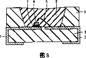
Fig. 8 shows the example of conventional semiconductors luminescent device.
Please referring to Fig. 8, resin part 3 forms by insert molding in the mode of fastening first lead frame 1 and second lead frame 2.Led chip 4 usefulness Ag ointment 7 are installed on first lead frame 1.Closing line 5 is connected to second lead frame 2.Led chip 4 is surrounded to be protected and to seal by epoxy resin 6.
The manufacture method of light emitting semiconductor device shown in Figure 8 will be described below.
When the mounted LEDs chip light emitting, produce heat.The quantity of the heat of described generation is proportional with the electric current that flows through led chip.Along with the led chip temperature uprises, the luminous efficiency step-down of led chip causes light attenuation.In other words,, also can't obtain brighter light effectively even adopt very big electric current, and the lifetime of led chip.
Drain into outside to reduce the temperature of led chip, even the led chip that also can show good luminous efficient and have good endurance life characteristic under big current conditions can be provided by the heat that led chip is produced.
For example, following example is the conventional semiconductors luminescent device that purpose is to improve radiation efficiency: the open No.11-46018 (conventional example 1) of Japan Patent, the open No.2002-222998 (conventional example 2) of Japan Patent, the open No.2000-58924 (conventional example 3) of Japan Patent, the open No.2000-77725 (conventional example 4) of Japan Patent and the open No.2000-216443 (conventional example 5) of Japan Patent.
In conventional example 1 and 2, improve thermal radiation by the surface area that increases lead frame.In conventional example 3,4 and 5, improve thermal radiation by using the thermal conductivity metal higher than the thermal conductivity of the resin that is used for base material.
But, by lead frame is adopted non-linear configurations increase the LED side lead frame surface area or be subjected to encapsulating the relative restriction of finite size as increase thickness as described in the conventional example 1 and 2.Only change the surface area that structure can not increase lead frame effectively.Therefore, radiation efficiency can not be enhanced enough grades.
Because lead frame will be bent in subsequent step, lead frame can not be made blocked uply.In addition, compare with thin lead frame, thicker lead frame is needing bigger strength when sheet spare is gone out lead frame.Correspondingly, the thickness of mould must increase to guarantee the intensity of mould, causes that punching out partly is slit wideer between the lead frame.Common described slit need equal the thickness of lead frame, and perhaps at least 3/4 of lead frame thickness.If the slit between the lead frame increases, just can not provide effective area to engage, perhaps the lead frame area will diminish.
The another kind of method relevant with radiation efficiency is lead frame terminal on the part of increase LED element and the contact area between the mounting panel.Have superiority though do like this from the thermal radiation aspect, the heat in the welding process will be easy to be passed to the LED device, thus the negative effect reliability.
Under the situation of metal as substrate that the employing thermal conductivity is higher than resin as described in conventional example 3,4 and 5, identical with above-mentioned situation, the heat in the welding process might the negative effect reliability.
Summary of the invention
In view of above-mentioned each side, an object of the present invention is to provide a kind of light emitting semiconductor device and manufacture method thereof, described light emitting semiconductor device shows high thermal radiation property and good illumination efficiency and endurance life characteristic, and can not reduce the machinability of lead frame and the reliability of led chip.
According to an aspect of the present invention, a kind of light emitting semiconductor device comprises: led chip; First lead frame has been installed described led chip on it; Second lead frame, it is electrically connected to described led chip by electric wire; The resin part, it is around peripheral and fastening described first and second lead frames of described led chip; Wherein metallic object is positioned under the zone that led chip has been installed on first lead frame, and this metallic object is configured to more downward more outstanding than the resin part of fastening described first and second lead frames.
According to a further aspect in the invention, provide a kind of light emitting semiconductor device, comprising: led chip; Metallic object has been installed described led chip on it; First lead frame, it is electrically connected to described metallic object; Second lead frame, it is electrically connected to described led chip by electric wire; The resin part, it is around peripheral and fastening described first and second lead frames of described metallic object and led chip; Wherein said metallic object is configured to more downward more outstanding than the resin part of fastening described first and second lead frames.
According to a further aspect in the invention, provide a kind of light emitting semiconductor device, comprising: led chip; Metallic object has been installed described led chip on it; First lead frame, it is electrically connected to described metallic object; Second lead frame, it is electrically connected to described led chip by electric wire; The resin part, it is around peripheral and fastening described first and second lead frames of described metallic object and led chip; Wherein said metallic object has the top that is processed as inverted frustum of a cone structure, and described top is assemblied in described first lead frame.
Therefore, heat can be passed to described metallic object effectively from first lead frame.Therefore can provide the light emitting semiconductor device that shows remarkable thermal radiation property.
Described metallic object can leave first lead frame or contact with first lead frame.All set up the electric insulation of lead frame in both cases.
Carry out on the surface of described metallic object under the situation of electric insulation processing, preferably surperficial and first lead frame that carries out the metallic object of electric insulation processing forms and contacts.Therefore, the thermal radiation of light emitting semiconductor device can improve.
Described light emitting semiconductor device preferably includes a plurality of led chips.Therefore, can strengthen applicability such as products such as full-color displays.
Therefore, the heat of led chip generation directly is passed to mounting panel by metallic object.Therefore improved thermal radiation.
Preferably, the top of described metallic object forms inverted frustum of a cone structure, and described top is assemblied in first lead frame.Therefore, described metallic object is securely fixed on the lead frame.By the reflection effect of described inverted frustum of a cone structure, the luminous intensity of described light emitting semiconductor device strengthens.
In above-mentioned light emitting semiconductor device, described metallic object preferably includes at least a material of selecting from the group that comprises copper, aluminium, copper alloy and aluminium alloy.The advantage of these metals is that the thermal radiation of described light emitting semiconductor device can improve by high-heating radiation.
According to an aspect of fabricating method of semiconductor light-emitting device of the present invention, it comprises the following steps: to form the resin part that keeps first and second lead frames and be positioned at the metallic object under described first lead frame by insert molding; Led chip is installed on described first lead frame.
According to another aspect of fabricating method of semiconductor light-emitting device of the present invention, it comprises the following steps: to form resin part that keeps first and second lead frames and the metallic object that is electrically connected described first lead frame by insert molding; Led chip is installed on the described metallic object.
According to another aspect of fabricating method of semiconductor light-emitting device of the present invention, it comprises the following steps: to form maintenance first and second lead frames and have the resin part that is positioned at the depression under described first lead frame by insert molding; Metallic object is connected to described depression; And led chip is installed on described first lead frame.
According to another aspect of fabricating method of semiconductor light-emitting device of the present invention, it comprises the following steps: to form maintenance first and second lead frames and have the resin part that is positioned at the depression under described first lead frame by insert molding; Metallic object is connected to described depression; And led chip is installed on the described metallic object.
Therefore, the heat that produces at the led chip place can be passed to mounting panel by described metallic object, and described metallic object is positioned at first lead frame and has installed under the zone of led chip.The light emitting semiconductor device of heat-radiating properties brilliance can be provided.
According to another aspect of the present invention, fabricating method of semiconductor light-emitting device comprises the following steps: to form the resin part that keeps first and second lead frames and have depression by insert molding; Metallic object is connected to described depression; And led chip is installed on the described metallic object or first lead frame.
Above-mentioned fabricating method of semiconductor light-emitting device also comprises the step of described metallic object and first lead frame being carried out joint filling (caulking).Preferably, in the joint filling step inverted frustum of a cone being processed at the top of described metallic object constructs.By described joint filling step, the described metallic object and first lead frame are firmly fixed more.And by the reflection effect of described inverted frustum of a cone structure, the luminous intensity of described light emitting semiconductor device strengthens.
According to light emitting semiconductor device of the present invention and manufacture method thereof, the heat that produces at the led chip place drains into mounting panel by metallic object, and described metallic object is positioned at first lead frame and has installed under the zone of led chip.Do not need to use thick lead frame.Therefore can prevent the deterioration of the machinability of lead frame.In addition, the heat in the welding process is difficult for being passed to LED.Therefore, the light emitting semiconductor device that shows high thermal radiation property and good illumination efficiency and endurance life characteristic can be provided, and can not reduce the machinability of lead frame and the reliability of led chip.
By detailed description below in conjunction with accompanying drawing, above-mentioned and other purposes of the present invention, characteristic, aspect and the advantage easy to understand that will become.
Description of drawings
Fig. 1 to Fig. 5 is respectively the sectional view of the surface-mounted LED of first to the 5th embodiment according to the present invention;
Fig. 6 A and Fig. 6 B have represented according to the installation of the 6th embodiment the manufacture method of the substrate of LED, wherein Fig. 6 A is arranged on situation in the insert molding mould corresponding to lead frame and metallic object, and Fig. 6 B has shown the resin part after lead frame and metallic object insert molding are finished;
Fig. 7 A, Fig. 7 B and Fig. 7 C have represented according to the installation of the 7th embodiment the manufacture method of the substrate of LED, wherein Fig. 7 A is arranged on situation in the insert molding mould corresponding to lead frame, Fig. 7 B has shown the resin part after the lead frame insert molding is finished, and Fig. 7 C is inserted into the situation in the depression of resin part corresponding to metallic object;
Fig. 8 is the sectional view of conventional semiconductors luminescent device example.
Embodiment
The embodiment of light emitting semiconductor device and manufacture method thereof will be described below.
The embodiment of light emitting semiconductor device at first is described with reference to Fig. 1-5.
In following first to the 5th embodiment, the quantity of mounted LEDs chip 4 is preferably a plurality of.Therefore, the light emitting semiconductor device applicability that is used for products such as full-color display can strengthen.Be installed under the situation on the product at a plurality of led chips, strict owing to produce a large amount of heats to thermal radiation.Present embodiment is particularly conducive to head it off.
First embodiment
Fig. 1 is the sectional view according to the surface-mounted LED of first embodiment of the invention.
The light emitting semiconductor device of first embodiment comprises: led chip 4; First lead frame 1 has been installed led chip 4 on it; Second lead frame 2, it is electrically connected to led chip 4 by the closing line such as gold thread 5; Resin part 3, it is around also fixing described lead frame around the led chip 4.Metallic object 8 is positioned under the zone that led chip 4 has been installed on first lead frame 1.
In first embodiment, metallic object 8 preferably leaves first lead frame 1 and second lead frame 2.
The reason that the slit is set between first lead frame 1 and second lead frame 2 and metallic object 8 is, prevent first lead frame 1 that separately forms with second lead frame 2 because above-mentioned contacting and short circuit therebetween.In first embodiment, the heat that is produced by led chip 4 sequentially transmits by the slit between first lead frame 1, first lead frame 1 and the metallic object 8, subsequently to metallic object 8, thereby drains into mounting panel.For the heat that led chip 4 is produced is passed to metallic object 8 effectively, above-mentioned slit is preferably as far as possible little.Preferably, the volume of metallic object 8 in encapsulation is big as much as possible in encapsulation.
Preferably, metallic object 8 comprises at least a material of selecting from the group that comprises copper, aluminium, copper alloy and aluminium alloy.Because these metal ground high-heating radiations, from improving heat-radiating properties, it is preferred doing like this.The material of metallic object 8 is not limited to above-mentioned material, as long as have high thermal radiation, the other materials outside the metal (for example pottery) also can use.Though the thermal conductivity that it may be noted that pottery than metal difference, insulate.Therefore, under the situation that adopts pottery, the ceramic body corresponding with metallic object 8 can contact with first lead frame 1 and second lead frame 2, needn't carry out insulation processing from the teeth outwards.
Be positioned at led chip 4 resin part 3 on every side and formed by the white resin with high reflectance, purpose is to reflect effectively from led chip 4 to send ground light.In addition, in order to improve the output for the front side effectively, inner peripheral surface forms inverted frustum of a cone structure.At the light emitting semiconductor device of first embodiment, adopt the good resin of thermal conductivity to come as resin part 3, because described light emitting semiconductor device will be surface-mounted element by following process.Especially, liquid crystal polymer, polyamides amine type resin etc. can satisfy above-mentioned instructions for use.Needing under the situation of large area light emitting, the inner peripheral surface of resin part 3 can adopt the structure of being inverted outside the frustum of a cone structure, for example the inversion butt of pyramid structure.
Epoxy resin 6 is used to protect the LED componentry.Epoxy resin 6 is transparent or milky, and mainly introduces by embedding.As selection, can adopt transfer moudling, injection molding etc.In this case, luminous component can adopt structure (lens shaped etc.) arbitrarily.
In first embodiment, when when the plane is seen, metallic object 8 is positioned near the center of resin part 3, and will directly not run into the heat towards mounting panel that produces in the welding step process.Therefore, the heat that produces in welding process can not make the reliability of led chip reduce.
Consider above-mentioned aspect, the light emitting semiconductor device of first embodiment is better than the conventional semiconductors luminescent device, because can improve thermal radiation at an easy rate.
Second embodiment
Fig. 2 is the sectional view according to the surface-mounted LED of second embodiment of the invention.
The light emitting semiconductor device of second embodiment is the improvement of the light emitting semiconductor device of first embodiment.Metallic object 8 contacts with first lead frame 1.
For example, first lead frame 1 that led chip 4 has been installed is set to and is lower than second lead frame 2, thereby has set up and the contacting of metallic object 8.In example shown in Figure 2, first lead frame 1 is bent to form and the contacting of metallic object 8.
Therefore, the heat that is produced by led chip 4 sequentially transmits by first lead frame 1, metallic object 8 and mounting panel.Do not have the slit among first embodiment between first lead frame 1 and the metallic object 8, thereby the heat that led chip 4 places produce more effectively is passed to mounting panel.Though first lead frame 1 is bent forming and the contacting of metallic object 8 in the present embodiment, the profile by change metallic object 8 rather than revise first lead frame 1 and just can realize identical purpose.For example, can on the top plan of metallic object 8, form projection.
Consider above-mentioned aspect, the light emitting semiconductor device of present embodiment is compared aspect the thermal radiation with the light emitting semiconductor device of first embodiment improvement.
The 3rd embodiment
Fig. 3 is the sectional view according to the surface-mounted LED of third embodiment of the invention.
The light emitting semiconductor device of the 3rd embodiment is that the another one of the light emitting semiconductor device of first embodiment is improved.On the surface of metallic object 8, be provided with for example electric insulation processing section 9 by applying insulation film, insulating coating or forming by anodization.Carry out the surface formation of metallic object 8 and contacting of first lead frame 1 and second lead frame 2 of insulation processing.
In the light emitting semiconductor device of second embodiment, no matter be to adopt single led chip or a plurality of led chip, as long as led chip is positioned on the identical lead frame, the heat that is produced by led chip 4 can be passed to mounting panel, does not have the corresponding part in slit among first embodiment between first lead frame 1 and the metallic object 8.
Under a plurality of led chips 4 are positioned at situation on the different lead frames,, have only a lead frame to contact with metallic object 8 for the pattern short circuit of each lead frame of preventing to separate formation.This means and exist thermal radiation to improve restricted pattern part.
The feature that has the 3rd embodiment of identical purpose with first embodiment is owing to be provided with electric insulation processing section 9 on metallic object 8, even the pattern of all lead frames contacts with metallic object 8, also can not be short-circuited.
The advantage of the 3rd embodiment is, even be positioned on the different lead frames when a plurality of led chips 4, also can stably improve thermal radiation.Except the transmission path of first lead frame 1, metallic object 8 and mounting panel, the heat that led chip 4 produces can be passed to mounting panel by second lead frame 2.
The 4th embodiment
Fig. 4 is the sectional view according to the surface-mounted LED of fourth embodiment of the invention.
The light emitting semiconductor device of the 4th embodiment comprises: led chip 4; Metallic object 8 has been installed led chip 4 on it; First lead frame 1, it is electrically connected to metallic object 8; Second lead frame 2, it is electrically connected to led chip 4 by the closing line such as gold thread 5; Resin part 3, it is around around metallic object 8 and the led chip 4 and fix first and second lead frames.
The feature of the 4th embodiment is that led chip 4 is directly installed on the metallic object 8.The heat that is produced by led chip 4 directly is passed to metallic object 8 to be passed to mounting panel by metallic object 8.Therefore, compare with first to the 3rd embodiment, heat can obtain more effective radiation.
The 5th embodiment
Fig. 5 is the sectional view according to the surface-mounted LED of fifth embodiment of the invention.
In the 5th embodiment, the top of metallic object 8 forms has inverted frustum of a cone structure.The top of metallic object 8 is assemblied in first lead frame 1.The metallic object 8 and first lead frame 1 become one by joint filling.The top of metallic object 8 forms inverted frustum of a cone structure in the joint filling step.Therefore, the metallic object 8 and first lead frame 1 are firmly fixed.In addition, by described inverted frustum of a cone structure ground reflection effect, the luminous intensity of light emitting semiconductor device strengthens.The top of metallic object 8 is not limited to above-mentioned inversion frustum of a cone structure.For example, can adopt the inversion butt structure of pyramid.
Be fixed on the 6th and the 7th relevant embodiment of resin part 3 with metallic object 8 and describe with Fig. 7 C pair with reference to Fig. 6 A, Fig. 6 B and Fig. 7 A, Fig. 7 B below.
The 6th embodiment
Fig. 6 A and Fig. 6 B represent according to the manufacture method that the substrate of LED has been installed on its of the 6th embodiment.
The manufacture method of the 6th embodiment comprises the following steps: to form the resin part 3 that keeps metallic object 8 and lead frame 10 by insert molding; And led chip 4 is installed on described metallic object 8 or lead frame 10.Fig. 6 A and Fig. 6 B are installed in situation on the lead frame 10 corresponding to led chip 4.
As shown in Figure 6A, lead frame 10 and metallic object 8 almost are set at the insert molding mould 11 that is used for insert molding simultaneously.Therefore, formed resin part 3, thus lead frame 10 and metallic object 8 is integrated, shown in Fig. 6 B.Subsequently, led chip 4 usefulness Ag ointment are installed on the lead frame.Led chip 4 is connected to another lead frame by closing line.
The 7th embodiment
Fig. 7 A, Fig. 7 B and Fig. 7 C represent according to the manufacture method that the substrate of LED has been installed on its of the 7th embodiment.
The manufacture method of the 7th embodiment comprises the following steps: to have the resin part 3 of depression 13 to keep lead frame 10 by insert molding formation; Metallic object 8 is connected to depression 13; And led chip 4 is installed on described metallic object 8 or the lead frame 10.
Shown in Fig. 7 A, lead frame 10 is set in the insert molding mould 11, and insert molding mould 11 has the metallic object that is used for insert molding and inserts zone formation mould 12.Therefore, shown in Fig. 7 B, can form the resin part 3 that keeps lead frame 10 and have depression 13.Please referring to 7C, metallic object 8 is inserted in the depression 13 in the resin part 3 of carrying out above-mentioned molding step, and uses adhesive etc. to firmly fix.By with the 6th embodiment subsequent step similarly, led chip 4 is installed on the lead frame.Led chip 4 is connected to other lead frame by closing line.
The present invention so far is illustrated in conjunction with the preferred embodiments.But those of ordinary skill is appreciated that and the invention is not restricted to previous embodiment, and can make amendment in a different manner within the scope of the invention.
Claims (9)
1. light emitting semiconductor device comprises:
Led chip (4);
First lead frame (1) has been installed described led chip (4) on it;
Second lead frame (2), it is electrically connected to described led chip (4) by electric wire (5);
Resin part (3), it is around peripheral and fastening described first and second lead frames (1,2) of described led chip (4);
Wherein metallic object (8) is positioned under the zone that led chip (4) have been installed on first lead frame (1), and this metallic object is configured to more downward more outstanding than the resin part of fastening described first and second lead frames.
2. according to the light emitting semiconductor device described in the claim 1, it is characterized in that described metallic object (8) leaves described first and second lead frames (1,2).
3. according to the light emitting semiconductor device described in the claim 1, it is characterized in that described metallic object (8) contacts with described first lead frame (1).
4. according to the light emitting semiconductor device described in the claim 1, it is characterized in that
Described metallic object (8) has the surface of having carried out the electric insulation processing;
The described surface that described metallic object (8) has carried out the electric insulation processing contacts with first lead frame (1) formation.
5. according to the light emitting semiconductor device described in the claim 1, it is characterized in that comprising a plurality of led chips (4).
6. according to the light emitting semiconductor device described in the claim 1, it is characterized in that described metallic object (8) comprises at least a material of selecting from the group that comprises copper, aluminium, copper alloy and aluminium alloy.
7. light emitting semiconductor device comprises:
Led chip (4);
Metallic object (8) has been installed described led chip (4) on it;
First lead frame (1), it is electrically connected to described metallic object (8);
Second lead frame (2), it is electrically connected to described led chip (4) by electric wire (5);
Resin part (3), it is around peripheral and fastening described first and second lead frames (1,2) of described metallic object (8) and led chip (4);
Wherein said metallic object (8) is configured to more downward more outstanding than the resin part of fastening described first and second lead frames.
8. light emitting semiconductor device comprises:
Led chip (4);
Metallic object (8) has been installed described led chip (4) on it;
First lead frame (1), it is electrically connected to described metallic object (8);
Second lead frame (2), it is electrically connected to described led chip (4) by electric wire (5);
Resin part (3), it is around peripheral and fastening described first and second lead frames (1,2) of described metallic object (8) and led chip (4);
Wherein said metallic object (8) has the top that is processed as inverted frustum of a cone structure, and
Described top is assemblied in described first lead frame (1).
9. according to the light emitting semiconductor device described in claim 7 or 8, it is characterized in that described metallic object (8) comprises at least a material of selecting from the group that comprises copper, aluminium, copper alloy and aluminium alloy.
Applications Claiming Priority (2)
| Application Number | Priority Date | Filing Date | Title |
|---|---|---|---|
| JP2003000216A JP3910144B2 (en) | 2003-01-06 | 2003-01-06 | Semiconductor light emitting device and manufacturing method thereof |
| JP2003000216 | 2003-01-06 |
Related Child Applications (1)
| Application Number | Title | Priority Date | Filing Date |
|---|---|---|---|
| CNB2007100047826A Division CN100466312C (en) | 2003-01-06 | 2003-12-12 | Semiconductor light emitting device and fabrication method thereof |
Publications (2)
| Publication Number | Publication Date |
|---|---|
| CN1518135A CN1518135A (en) | 2004-08-04 |
| CN1306626C true CN1306626C (en) | 2007-03-21 |
Family
ID=32708764
Family Applications (2)
| Application Number | Title | Priority Date | Filing Date |
|---|---|---|---|
| CNB2007100047826A Expired - Fee Related CN100466312C (en) | 2003-01-06 | 2003-12-12 | Semiconductor light emitting device and fabrication method thereof |
| CNB2003101205693A Expired - Fee Related CN1306626C (en) | 2003-01-06 | 2003-12-12 | Semiconductor luminescent device and its manufacturing method |
Family Applications Before (1)
| Application Number | Title | Priority Date | Filing Date |
|---|---|---|---|
| CNB2007100047826A Expired - Fee Related CN100466312C (en) | 2003-01-06 | 2003-12-12 | Semiconductor light emitting device and fabrication method thereof |
Country Status (3)
| Country | Link |
|---|---|
| US (1) | US7012277B2 (en) |
| JP (1) | JP3910144B2 (en) |
| CN (2) | CN100466312C (en) |
Families Citing this family (60)
| Publication number | Priority date | Publication date | Assignee | Title |
|---|---|---|---|---|
| JP4174823B2 (en) * | 2003-03-27 | 2008-11-05 | サンケン電気株式会社 | Semiconductor light emitting device |
| JP2006049442A (en) * | 2004-08-02 | 2006-02-16 | Sharp Corp | Semiconductor light emission device and its manufacturing method |
| CN100340008C (en) * | 2004-09-30 | 2007-09-26 | 中国科学院半导体研究所 | Method for making GaN-based LED with back hole structure |
| EP1825524A4 (en) * | 2004-12-16 | 2010-06-16 | Seoul Semiconductor Co Ltd | Leadframe having a heat sink supporting ring, fabricating method of a light emitting diodepackage using the same and light emitting diodepackage fabbricated by the method |
| US20060131734A1 (en) * | 2004-12-17 | 2006-06-22 | Texas Instruments Incorporated | Multi lead frame power package |
| JP4606302B2 (en) * | 2005-01-27 | 2011-01-05 | 京セラ株式会社 | Light emitting device |
| JP4606382B2 (en) * | 2005-01-27 | 2011-01-05 | 京セラ株式会社 | Light emitting device |
| KR100638721B1 (en) * | 2005-01-28 | 2006-10-30 | 삼성전기주식회사 | Side view led package having lead frame structure designed for improving resin flow |
| KR100631901B1 (en) * | 2005-01-31 | 2006-10-11 | 삼성전기주식회사 | LED package frame and LED package employing the same |
| JP2006237464A (en) * | 2005-02-28 | 2006-09-07 | Matsushita Electric Ind Co Ltd | Semiconductor light emitting device |
| JP4948777B2 (en) * | 2005-03-16 | 2012-06-06 | ローム株式会社 | Optical communication module |
| WO2006095676A1 (en) * | 2005-03-07 | 2006-09-14 | Rohm Co., Ltd. | Optical communication module and manufacturing method thereof |
| WO2006095949A1 (en) * | 2005-03-11 | 2006-09-14 | Seoul Semiconductor Co., Ltd. | Led package having an array of light emitting cells coupled in series |
| KR100593935B1 (en) | 2005-03-24 | 2006-06-30 | 삼성전기주식회사 | Light emitting diode package and method for manufacturing the same |
| KR100690313B1 (en) * | 2005-04-28 | 2007-03-09 | (주) 아모센스 | Electron parts package |
| KR100690314B1 (en) | 2005-04-28 | 2007-03-09 | (주) 아모센스 | Electron parts package |
| KR100662844B1 (en) | 2005-06-10 | 2007-01-02 | 삼성전자주식회사 | Led package structure and manufacturing method, and led array module |
| US7800124B2 (en) | 2005-06-30 | 2010-09-21 | Panasonic Electric Works Co., Ltd. | Light-emitting device |
| JP5054331B2 (en) * | 2005-06-30 | 2012-10-24 | パナソニック株式会社 | Lighting equipment using LED |
| KR100632003B1 (en) * | 2005-08-08 | 2006-10-09 | 삼성전기주식회사 | Led package having recess in heat transfer part |
| US20070063213A1 (en) * | 2005-09-21 | 2007-03-22 | Lighthouse Technology Co., Ltd. | LED package |
| JP5038623B2 (en) * | 2005-12-27 | 2012-10-03 | 株式会社東芝 | Optical semiconductor device and manufacturing method thereof |
| US8044412B2 (en) | 2006-01-20 | 2011-10-25 | Taiwan Semiconductor Manufacturing Company, Ltd | Package for a light emitting element |
| JP2007208061A (en) * | 2006-02-02 | 2007-08-16 | Sharp Corp | Semiconductor light emitting element, manufacturing method thereof, and assembly thereof |
| US7365407B2 (en) * | 2006-05-01 | 2008-04-29 | Avago Technologies General Ip Pte Ltd | Light emitting diode package with direct leadframe heat dissipation |
| WO2007135707A1 (en) | 2006-05-18 | 2007-11-29 | Nichia Corporation | Resin molded body and surface-mounted light emitting device, and manufacturing method thereof |
| TWI384655B (en) * | 2006-06-27 | 2013-02-01 | Seoul Semiconductor Co Ltd | Side view type led package |
| KR100904152B1 (en) * | 2006-06-30 | 2009-06-25 | 서울반도체 주식회사 | Leadframe having a heat sink supporting part, fabricating method of the light emitting diode package using the same and light emitting diode package fabricated by the method |
| TWM309757U (en) * | 2006-09-19 | 2007-04-11 | Everlight Electronics Co Ltd | Side view LED package structure |
| KR100730771B1 (en) * | 2006-10-11 | 2007-06-21 | 주식회사 쎄라텍 | Package for light emission device |
| KR100788931B1 (en) | 2006-10-27 | 2007-12-27 | (주) 아모센스 | Electron components package |
| JP5380774B2 (en) | 2006-12-28 | 2014-01-08 | 日亜化学工業株式会社 | Surface mount type side surface light emitting device and manufacturing method thereof |
| TWI325186B (en) * | 2007-01-19 | 2010-05-21 | Harvatek Corp | Led chip package structure using ceramic material as a substrate |
| JP4960194B2 (en) * | 2007-10-22 | 2012-06-27 | 電気化学工業株式会社 | Method for manufacturing substrate for light emitting device package and light emitting device package |
| JP5294741B2 (en) * | 2008-07-14 | 2013-09-18 | 日亜化学工業株式会社 | RESIN MOLDED BODY, SURFACE MOUNTED LIGHT EMITTING DEVICE AND METHOD FOR PRODUCING THEM |
| DE102008045925A1 (en) * | 2008-09-04 | 2010-03-11 | Osram Opto Semiconductors Gmbh | Optoelectronic component and method for producing an optoelectronic component |
| US20110260192A1 (en) * | 2008-10-01 | 2011-10-27 | Chang Hoon Kwak | Light-emitting diode package using a liquid crystal polymer |
| KR101007131B1 (en) * | 2008-11-25 | 2011-01-10 | 엘지이노텍 주식회사 | Light emitting device package |
| KR101047801B1 (en) * | 2008-12-29 | 2011-07-07 | 엘지이노텍 주식회사 | Light emitting device package and manufacturing method thereof |
| JP2010171073A (en) * | 2009-01-20 | 2010-08-05 | Showa Denko Kk | Light-emitting device, electrical device, and display |
| WO2010095482A2 (en) * | 2009-02-20 | 2010-08-26 | 三洋電機株式会社 | Substrate for electronic components, light emitting device, and production method for substrate for electronic components |
| US9385285B2 (en) | 2009-09-17 | 2016-07-05 | Koninklijke Philips N.V. | LED module with high index lens |
| EP2346100B1 (en) * | 2010-01-15 | 2019-05-22 | LG Innotek Co., Ltd. | Light emitting apparatus and lighting system |
| US9024350B2 (en) * | 2010-02-08 | 2015-05-05 | Ban P Loh | LED light module |
| US8525213B2 (en) | 2010-03-30 | 2013-09-03 | Lg Innotek Co., Ltd. | Light emitting device having multiple cavities and light unit having the same |
| US8269244B2 (en) * | 2010-06-28 | 2012-09-18 | Cree, Inc. | LED package with efficient, isolated thermal path |
| WO2012067203A1 (en) * | 2010-11-19 | 2012-05-24 | 旭硝子株式会社 | Substrate for light-emitting element, and light-emitting device |
| JP2014029890A (en) * | 2010-11-19 | 2014-02-13 | Asahi Glass Co Ltd | Substrate for light-emitting element and light-emitting device |
| US9716061B2 (en) * | 2011-02-18 | 2017-07-25 | 3M Innovative Properties Company | Flexible light emitting semiconductor device |
| DE102011101052A1 (en) * | 2011-05-09 | 2012-11-15 | Heraeus Materials Technology Gmbh & Co. Kg | Substrate with electrically neutral region |
| KR101824011B1 (en) * | 2011-07-29 | 2018-01-31 | 엘지이노텍 주식회사 | Light-emitting device |
| JP5813467B2 (en) * | 2011-11-07 | 2015-11-17 | 新光電気工業株式会社 | Substrate, light emitting device, and method of manufacturing substrate |
| US10043960B2 (en) * | 2011-11-15 | 2018-08-07 | Cree, Inc. | Light emitting diode (LED) packages and related methods |
| US8698291B2 (en) * | 2011-12-15 | 2014-04-15 | Freescale Semiconductor, Inc. | Packaged leadless semiconductor device |
| JP5978631B2 (en) * | 2012-01-26 | 2016-08-24 | 日亜化学工業株式会社 | Light emitting device |
| US8917010B2 (en) * | 2012-02-02 | 2014-12-23 | Citizen Electronics Co., Ltd. | Lighting device including phosphor layer and light-transmitting layer that is arranged in contact with the phosphor layer to release static charge to substrate |
| JP6147976B2 (en) * | 2012-09-26 | 2017-06-14 | ローム株式会社 | LIGHT EMITTING DEVICE AND LIGHT EMITTING UNIT MANUFACTURING METHOD |
| DE102012110261A1 (en) * | 2012-10-26 | 2014-04-30 | Osram Gmbh | Housing for an optoelectronic component and method for producing a housing |
| US10403792B2 (en) * | 2016-03-07 | 2019-09-03 | Rayvio Corporation | Package for ultraviolet emitting devices |
| US20170356640A1 (en) | 2016-06-10 | 2017-12-14 | Innotec, Corp. | Illumination assembly including thermal energy management |
Citations (1)
| Publication number | Priority date | Publication date | Assignee | Title |
|---|---|---|---|---|
| JP2004009384A (en) * | 2002-06-04 | 2004-01-15 | Dainippon Printing Co Ltd | Method for generating data for control mark and system |
Family Cites Families (27)
| Publication number | Priority date | Publication date | Assignee | Title |
|---|---|---|---|---|
| JPH0680748B2 (en) * | 1986-03-31 | 1994-10-12 | 株式会社東芝 | Resin-sealed semiconductor device |
| US5367196A (en) * | 1992-09-17 | 1994-11-22 | Olin Corporation | Molded plastic semiconductor package including an aluminum alloy heat spreader |
| DE19621124A1 (en) * | 1996-05-24 | 1997-11-27 | Siemens Ag | Optoelectronic converter and its manufacturing process |
| DE19638667C2 (en) * | 1996-09-20 | 2001-05-17 | Osram Opto Semiconductors Gmbh | Mixed-color light-emitting semiconductor component with luminescence conversion element |
| JPH10125826A (en) * | 1996-10-24 | 1998-05-15 | Hitachi Ltd | Semiconductor device and manufacture thereof |
| JPH1146018A (en) | 1997-07-28 | 1999-02-16 | Citizen Electron Co Ltd | Surface mounted type light-emitting diode |
| DE19746893B4 (en) * | 1997-10-23 | 2005-09-01 | Siemens Ag | Optoelectronic component with heat sink in the base part and method for the production |
| JP3518843B2 (en) | 1998-10-13 | 2004-04-12 | 株式会社トクヤマ | Metallized substrate |
| JPH11177129A (en) * | 1997-12-16 | 1999-07-02 | Rohm Co Ltd | Chip type led, led lamp and led display |
| KR100259080B1 (en) * | 1998-02-11 | 2000-06-15 | 김영환 | Lead frame having heat spread and semiconductor package with such lead frame |
| JP3356069B2 (en) * | 1998-07-29 | 2002-12-09 | 松下電器産業株式会社 | Chip type light emitting device |
| JP2000058924A (en) | 1998-08-06 | 2000-02-25 | Shichizun Denshi:Kk | Surface mounting-type light emitting diode and its manufacture |
| JP4215306B2 (en) | 1998-08-27 | 2009-01-28 | シチズン電子株式会社 | Semiconductor package and manufacturing method thereof |
| US6335548B1 (en) * | 1999-03-15 | 2002-01-01 | Gentex Corporation | Semiconductor radiation emitter package |
| JP2000216443A (en) * | 1999-01-25 | 2000-08-04 | Citizen Electronics Co Ltd | Surface mounted type led and its manufacture |
| DE10033502A1 (en) * | 2000-07-10 | 2002-01-31 | Osram Opto Semiconductors Gmbh | Optoelectronic module, process for its production and its use |
| US6561680B1 (en) * | 2000-11-14 | 2003-05-13 | Kelvin Shih | Light emitting diode with thermally conductive structure |
| JP4904623B2 (en) | 2001-01-29 | 2012-03-28 | 日亜化学工業株式会社 | Optical semiconductor element |
| ATE551731T1 (en) * | 2001-04-23 | 2012-04-15 | Panasonic Corp | LIGHT-EMITTING DEVICE HAVING A LIGHT-EMITTING DIODE CHIP |
| US20020163001A1 (en) * | 2001-05-04 | 2002-11-07 | Shaddock David Mulford | Surface mount light emitting device package and fabrication method |
| JP2003078219A (en) | 2001-09-04 | 2003-03-14 | Katsurayama Technol:Kk | Recessed printed wiring board and its manufacturing method |
| US20030058650A1 (en) * | 2001-09-25 | 2003-03-27 | Kelvin Shih | Light emitting diode with integrated heat dissipater |
| US6936855B1 (en) * | 2002-01-16 | 2005-08-30 | Shane Harrah | Bendable high flux LED array |
| JP3828036B2 (en) * | 2002-03-28 | 2006-09-27 | 三菱電機株式会社 | Manufacturing method and manufacturing apparatus for resin mold device |
| JP4280050B2 (en) | 2002-10-07 | 2009-06-17 | シチズン電子株式会社 | White light emitting device |
| TW578280B (en) * | 2002-11-21 | 2004-03-01 | United Epitaxy Co Ltd | Light emitting diode and package scheme and method thereof |
| US7095110B2 (en) * | 2004-05-21 | 2006-08-22 | Gelcore, Llc | Light emitting diode apparatuses with heat pipes for thermal management |
-
2003
- 2003-01-06 JP JP2003000216A patent/JP3910144B2/en not_active Expired - Fee Related
- 2003-12-12 CN CNB2007100047826A patent/CN100466312C/en not_active Expired - Fee Related
- 2003-12-12 CN CNB2003101205693A patent/CN1306626C/en not_active Expired - Fee Related
- 2003-12-23 US US10/745,764 patent/US7012277B2/en not_active Expired - Lifetime
Patent Citations (1)
| Publication number | Priority date | Publication date | Assignee | Title |
|---|---|---|---|---|
| JP2004009384A (en) * | 2002-06-04 | 2004-01-15 | Dainippon Printing Co Ltd | Method for generating data for control mark and system |
Also Published As
| Publication number | Publication date |
|---|---|
| CN1518135A (en) | 2004-08-04 |
| JP2004214436A (en) | 2004-07-29 |
| JP3910144B2 (en) | 2007-04-25 |
| CN1992365A (en) | 2007-07-04 |
| CN100466312C (en) | 2009-03-04 |
| US20040135156A1 (en) | 2004-07-15 |
| US7012277B2 (en) | 2006-03-14 |
Similar Documents
| Publication | Publication Date | Title |
|---|---|---|
| CN1306626C (en) | Semiconductor luminescent device and its manufacturing method | |
| CN100338786C (en) | Semiconductor light emitting device, method for producing the same and reflector for semiconductor light emitting device | |
| US8349627B2 (en) | Method for fabricating a light emitting diode package structure | |
| CN1871710A (en) | Power surface mount light emitting die package | |
| US9620693B2 (en) | Light emitting device and lighting system having the same | |
| TWI525848B (en) | Light emitting device, resin package, resin compact and method of manufacturing the same | |
| US9698312B2 (en) | Resin package and light emitting device | |
| TWI484666B (en) | Light emitting device | |
| US8450770B2 (en) | Light emitting package structure | |
| CN1898810A (en) | Package for light emitting device | |
| CN1638158A (en) | Surface mount type semiconductor device and lead frame structure thereof | |
| CN1822401A (en) | LED package frame and LED package having the same | |
| US8368085B2 (en) | Semiconductor package | |
| CN1825645A (en) | Led housing and fabrication method thereof | |
| CN1670973A (en) | High power LED package | |
| CN1744335A (en) | Surface mount LED | |
| CN1901190A (en) | Side view led with improved arrangement of protection device | |
| CN1959982A (en) | Semiconductor light emitting device | |
| CN1992362A (en) | Luminescent semiconductor device and method for manufacturing the same | |
| CN1825644A (en) | High power led housing and fabrication method thereof | |
| CN101051665A (en) | Light emitting diode package having anodized insulation layer and fabrication method therefor | |
| CN1929159A (en) | Semiconductor illumination device | |
| CN1617362A (en) | Light emitting element and light emitting device with the light emitting element and method for manufacturing the light emitting element | |
| CN1691361A (en) | Semiconductor light emitting device and fabrication method thereof | |
| CN1841801A (en) | Semiconductor light emitting device and semiconductor light emitting unit |
Legal Events
| Date | Code | Title | Description |
|---|---|---|---|
| C06 | Publication | ||
| PB01 | Publication | ||
| C10 | Entry into substantive examination | ||
| SE01 | Entry into force of request for substantive examination | ||
| C14 | Grant of patent or utility model | ||
| GR01 | Patent grant | ||
| CF01 | Termination of patent right due to non-payment of annual fee | ||
| CF01 | Termination of patent right due to non-payment of annual fee |
Granted publication date: 20070321 Termination date: 20211212 |