CN1280452C - Copper plating bath and method for plating substrate by using the same - Google Patents
Copper plating bath and method for plating substrate by using the same Download PDFInfo
- Publication number
- CN1280452C CN1280452C CN02809517.0A CN02809517A CN1280452C CN 1280452 C CN1280452 C CN 1280452C CN 02809517 A CN02809517 A CN 02809517A CN 1280452 C CN1280452 C CN 1280452C
- Authority
- CN
- China
- Prior art keywords
- copper
- substrate
- plating
- plating bath
- acid
- Prior art date
- Legal status (The legal status is an assumption and is not a legal conclusion. Google has not performed a legal analysis and makes no representation as to the accuracy of the status listed.)
- Expired - Lifetime
Links
- 239000000758 substrate Substances 0.000 title claims abstract description 349
- 238000007747 plating Methods 0.000 title claims abstract description 338
- 229910052802 copper Inorganic materials 0.000 title claims abstract description 180
- 239000010949 copper Substances 0.000 title claims abstract description 180
- RYGMFSIKBFXOCR-UHFFFAOYSA-N Copper Chemical compound [Cu] RYGMFSIKBFXOCR-UHFFFAOYSA-N 0.000 title claims abstract description 179
- 238000000034 method Methods 0.000 title claims abstract description 74
- 238000006243 chemical reaction Methods 0.000 claims abstract description 49
- 150000001875 compounds Chemical class 0.000 claims abstract description 28
- GYZLOYUZLJXAJU-UHFFFAOYSA-N diglycidyl ether Chemical compound C1OC1COCC1CO1 GYZLOYUZLJXAJU-UHFFFAOYSA-N 0.000 claims abstract description 26
- 125000001453 quaternary ammonium group Chemical group 0.000 claims abstract description 17
- 238000012545 processing Methods 0.000 claims description 107
- 238000000576 coating method Methods 0.000 claims description 64
- 239000003792 electrolyte Substances 0.000 claims description 56
- 239000011248 coating agent Substances 0.000 claims description 46
- QAOWNCQODCNURD-UHFFFAOYSA-N Sulfuric acid Chemical compound OS(O)(=O)=O QAOWNCQODCNURD-UHFFFAOYSA-N 0.000 claims description 22
- -1 sulfoalkyl sulfonic acid Chemical compound 0.000 claims description 22
- 239000002253 acid Substances 0.000 claims description 16
- 239000000654 additive Substances 0.000 claims description 14
- 229910000365 copper sulfate Inorganic materials 0.000 claims description 14
- ARUVKPQLZAKDPS-UHFFFAOYSA-L copper(II) sulfate Chemical compound [Cu+2].[O-][S+2]([O-])([O-])[O-] ARUVKPQLZAKDPS-UHFFFAOYSA-L 0.000 claims description 14
- 230000000996 additive effect Effects 0.000 claims description 13
- 229910052751 metal Inorganic materials 0.000 claims description 13
- 239000002184 metal Substances 0.000 claims description 13
- 150000007524 organic acids Chemical class 0.000 claims description 12
- 229910052799 carbon Inorganic materials 0.000 claims description 11
- QPLDLSVMHZLSFG-UHFFFAOYSA-N Copper oxide Chemical compound [Cu]=O QPLDLSVMHZLSFG-UHFFFAOYSA-N 0.000 claims description 10
- 238000004458 analytical method Methods 0.000 claims description 8
- 239000005749 Copper compound Substances 0.000 claims description 7
- 230000015572 biosynthetic process Effects 0.000 claims description 7
- 150000001880 copper compounds Chemical class 0.000 claims description 7
- 229910052500 inorganic mineral Inorganic materials 0.000 claims description 7
- 239000011707 mineral Substances 0.000 claims description 7
- ZAMOUSCENKQFHK-UHFFFAOYSA-N Chlorine atom Chemical compound [Cl] ZAMOUSCENKQFHK-UHFFFAOYSA-N 0.000 claims description 6
- DKVNPHBNOWQYFE-UHFFFAOYSA-N carbamodithioic acid Chemical class NC(S)=S DKVNPHBNOWQYFE-UHFFFAOYSA-N 0.000 claims description 6
- 239000000460 chlorine Substances 0.000 claims description 6
- 229910052801 chlorine Inorganic materials 0.000 claims description 6
- ORTQZVOHEJQUHG-UHFFFAOYSA-L copper(II) chloride Chemical compound Cl[Cu]Cl ORTQZVOHEJQUHG-UHFFFAOYSA-L 0.000 claims description 6
- 150000003839 salts Chemical class 0.000 claims description 6
- 150000003460 sulfonic acids Chemical class 0.000 claims description 6
- JPVYNHNXODAKFH-UHFFFAOYSA-N Cu2+ Chemical compound [Cu+2] JPVYNHNXODAKFH-UHFFFAOYSA-N 0.000 claims description 5
- KDLHZDBZIXYQEI-UHFFFAOYSA-N Palladium Chemical compound [Pd] KDLHZDBZIXYQEI-UHFFFAOYSA-N 0.000 claims description 5
- 239000005864 Sulphur Substances 0.000 claims description 5
- 229960004643 cupric oxide Drugs 0.000 claims description 5
- OKTJSMMVPCPJKN-UHFFFAOYSA-N Carbon Chemical group [C] OKTJSMMVPCPJKN-UHFFFAOYSA-N 0.000 claims description 4
- 238000007772 electroless plating Methods 0.000 claims description 4
- 238000005229 chemical vapour deposition Methods 0.000 claims description 3
- 229940116318 copper carbonate Drugs 0.000 claims description 3
- 229960000355 copper sulfate Drugs 0.000 claims description 3
- GEZOTWYUIKXWOA-UHFFFAOYSA-L copper;carbonate Chemical compound [Cu+2].[O-]C([O-])=O GEZOTWYUIKXWOA-UHFFFAOYSA-L 0.000 claims description 3
- 229960003280 cupric chloride Drugs 0.000 claims description 3
- 238000000151 deposition Methods 0.000 claims description 3
- 230000008021 deposition Effects 0.000 claims description 3
- PEVJCYPAFCUXEZ-UHFFFAOYSA-J dicopper;phosphonato phosphate Chemical compound [Cu+2].[Cu+2].[O-]P([O-])(=O)OP([O-])([O-])=O PEVJCYPAFCUXEZ-UHFFFAOYSA-J 0.000 claims description 3
- 229910052763 palladium Inorganic materials 0.000 claims description 3
- 239000012488 sample solution Substances 0.000 claims description 3
- 238000003672 processing method Methods 0.000 claims description 2
- 229910001431 copper ion Inorganic materials 0.000 claims 2
- 235000012976 tarts Nutrition 0.000 claims 2
- 239000004065 semiconductor Substances 0.000 abstract description 155
- XUIMIQQOPSSXEZ-UHFFFAOYSA-N Silicon Chemical compound [Si] XUIMIQQOPSSXEZ-UHFFFAOYSA-N 0.000 abstract description 11
- 229910052710 silicon Inorganic materials 0.000 abstract description 11
- 239000010703 silicon Substances 0.000 abstract description 11
- 150000001412 amines Chemical class 0.000 abstract description 10
- 239000000047 product Substances 0.000 abstract description 7
- 239000007859 condensation product Substances 0.000 abstract 1
- 238000005406 washing Methods 0.000 description 60
- 239000010408 film Substances 0.000 description 55
- 239000000243 solution Substances 0.000 description 51
- 238000001035 drying Methods 0.000 description 45
- 239000010410 layer Substances 0.000 description 44
- 238000005498 polishing Methods 0.000 description 44
- XLYOFNOQVPJJNP-UHFFFAOYSA-N water Substances O XLYOFNOQVPJJNP-UHFFFAOYSA-N 0.000 description 33
- 239000011148 porous material Substances 0.000 description 24
- 238000000137 annealing Methods 0.000 description 21
- 239000007789 gas Substances 0.000 description 21
- 239000007788 liquid Substances 0.000 description 19
- 238000011049 filling Methods 0.000 description 18
- 238000005259 measurement Methods 0.000 description 18
- 230000008569 process Effects 0.000 description 17
- 239000000523 sample Substances 0.000 description 16
- 238000005530 etching Methods 0.000 description 15
- 238000010521 absorption reaction Methods 0.000 description 14
- 239000002245 particle Substances 0.000 description 14
- 239000000126 substance Substances 0.000 description 14
- 241000370738 Chlorion Species 0.000 description 12
- 230000033001 locomotion Effects 0.000 description 12
- 101100493713 Caenorhabditis elegans bath-45 gene Proteins 0.000 description 11
- 238000000227 grinding Methods 0.000 description 11
- 230000000903 blocking effect Effects 0.000 description 10
- 238000004140 cleaning Methods 0.000 description 10
- 230000001681 protective effect Effects 0.000 description 10
- 235000012431 wafers Nutrition 0.000 description 10
- VYPSYNLAJGMNEJ-UHFFFAOYSA-N Silicium dioxide Chemical compound O=[Si]=O VYPSYNLAJGMNEJ-UHFFFAOYSA-N 0.000 description 9
- 230000036571 hydration Effects 0.000 description 9
- 238000006703 hydration reaction Methods 0.000 description 9
- 230000008676 import Effects 0.000 description 9
- 239000012528 membrane Substances 0.000 description 9
- 239000003566 sealing material Substances 0.000 description 9
- 230000032258 transport Effects 0.000 description 9
- KRHYYFGTRYWZRS-UHFFFAOYSA-N Fluorane Chemical compound F KRHYYFGTRYWZRS-UHFFFAOYSA-N 0.000 description 8
- 239000000463 material Substances 0.000 description 8
- 238000012546 transfer Methods 0.000 description 8
- 241000196324 Embryophyta Species 0.000 description 7
- AFVFQIVMOAPDHO-UHFFFAOYSA-N Methanesulfonic acid Chemical compound CS(O)(=O)=O AFVFQIVMOAPDHO-UHFFFAOYSA-N 0.000 description 7
- 239000003929 acidic solution Substances 0.000 description 7
- 150000001721 carbon Chemical group 0.000 description 7
- 238000010586 diagram Methods 0.000 description 7
- 230000000694 effects Effects 0.000 description 7
- 238000011156 evaluation Methods 0.000 description 7
- 238000002347 injection Methods 0.000 description 7
- 239000007924 injection Substances 0.000 description 7
- 239000007800 oxidant agent Substances 0.000 description 7
- 230000003647 oxidation Effects 0.000 description 7
- 238000007254 oxidation reaction Methods 0.000 description 7
- 230000002829 reductive effect Effects 0.000 description 7
- KRKNYBCHXYNGOX-UHFFFAOYSA-N citric acid Chemical compound OC(=O)CC(O)(C(O)=O)CC(O)=O KRKNYBCHXYNGOX-UHFFFAOYSA-N 0.000 description 6
- 238000001816 cooling Methods 0.000 description 6
- 238000009792 diffusion process Methods 0.000 description 6
- 125000004435 hydrogen atom Chemical group [H]* 0.000 description 6
- 238000011068 loading method Methods 0.000 description 6
- 239000000203 mixture Substances 0.000 description 6
- 238000000059 patterning Methods 0.000 description 6
- 238000011084 recovery Methods 0.000 description 6
- 239000013543 active substance Substances 0.000 description 5
- 125000000217 alkyl group Chemical group 0.000 description 5
- 239000003795 chemical substances by application Substances 0.000 description 5
- RTZKZFJDLAIYFH-UHFFFAOYSA-N ether Substances CCOCC RTZKZFJDLAIYFH-UHFFFAOYSA-N 0.000 description 5
- 238000012360 testing method Methods 0.000 description 5
- ROSDSFDQCJNGOL-UHFFFAOYSA-N Dimethylamine Chemical compound CNC ROSDSFDQCJNGOL-UHFFFAOYSA-N 0.000 description 4
- 230000006835 compression Effects 0.000 description 4
- 238000007906 compression Methods 0.000 description 4
- 239000008367 deionised water Substances 0.000 description 4
- 229910021641 deionized water Inorganic materials 0.000 description 4
- 239000003814 drug Substances 0.000 description 4
- 238000005516 engineering process Methods 0.000 description 4
- 238000007373 indentation Methods 0.000 description 4
- 238000009434 installation Methods 0.000 description 4
- 238000009413 insulation Methods 0.000 description 4
- 230000014759 maintenance of location Effects 0.000 description 4
- 230000000750 progressive effect Effects 0.000 description 4
- 230000000630 rising effect Effects 0.000 description 4
- 229910052814 silicon oxide Inorganic materials 0.000 description 4
- 238000003756 stirring Methods 0.000 description 4
- 125000002769 thiazolinyl group Chemical group 0.000 description 4
- 239000010409 thin film Substances 0.000 description 4
- MUBZPKHOEPUJKR-UHFFFAOYSA-N Oxalic acid Chemical compound OC(=O)C(O)=O MUBZPKHOEPUJKR-UHFFFAOYSA-N 0.000 description 3
- 229920003171 Poly (ethylene oxide) Polymers 0.000 description 3
- 239000004372 Polyvinyl alcohol Substances 0.000 description 3
- 125000001118 alkylidene group Chemical group 0.000 description 3
- 239000012298 atmosphere Substances 0.000 description 3
- 239000003153 chemical reaction reagent Substances 0.000 description 3
- 238000007599 discharging Methods 0.000 description 3
- 239000012530 fluid Substances 0.000 description 3
- 238000012423 maintenance Methods 0.000 description 3
- 238000004519 manufacturing process Methods 0.000 description 3
- 238000002156 mixing Methods 0.000 description 3
- 230000002093 peripheral effect Effects 0.000 description 3
- 229920002451 polyvinyl alcohol Polymers 0.000 description 3
- 229920000915 polyvinyl chloride Polymers 0.000 description 3
- 239000004800 polyvinyl chloride Substances 0.000 description 3
- 238000003892 spreading Methods 0.000 description 3
- 238000009423 ventilation Methods 0.000 description 3
- UWFRVQVNYNPBEF-UHFFFAOYSA-N 1-(2,4-dimethylphenyl)propan-1-one Chemical compound CCC(=O)C1=CC=C(C)C=C1C UWFRVQVNYNPBEF-UHFFFAOYSA-N 0.000 description 2
- CSCPPACGZOOCGX-UHFFFAOYSA-N Acetone Chemical compound CC(C)=O CSCPPACGZOOCGX-UHFFFAOYSA-N 0.000 description 2
- LYCAIKOWRPUZTN-UHFFFAOYSA-N Ethylene glycol Chemical compound OCCO LYCAIKOWRPUZTN-UHFFFAOYSA-N 0.000 description 2
- VEXZGXHMUGYJMC-UHFFFAOYSA-N Hydrochloric acid Chemical compound Cl VEXZGXHMUGYJMC-UHFFFAOYSA-N 0.000 description 2
- 235000011464 Pachycereus pringlei Nutrition 0.000 description 2
- 240000006939 Pachycereus weberi Species 0.000 description 2
- 235000011466 Pachycereus weberi Nutrition 0.000 description 2
- NSOXQYCFHDMMGV-UHFFFAOYSA-N Tetrakis(2-hydroxypropyl)ethylenediamine Chemical compound CC(O)CN(CC(C)O)CCN(CC(C)O)CC(C)O NSOXQYCFHDMMGV-UHFFFAOYSA-N 0.000 description 2
- 230000002159 abnormal effect Effects 0.000 description 2
- 239000006061 abrasive grain Substances 0.000 description 2
- 230000001133 acceleration Effects 0.000 description 2
- 230000003064 anti-oxidating effect Effects 0.000 description 2
- 239000011230 binding agent Substances 0.000 description 2
- 230000008859 change Effects 0.000 description 2
- 238000009833 condensation Methods 0.000 description 2
- 230000005494 condensation Effects 0.000 description 2
- 150000001879 copper Chemical class 0.000 description 2
- 239000013078 crystal Substances 0.000 description 2
- 238000009713 electroplating Methods 0.000 description 2
- 230000003628 erosive effect Effects 0.000 description 2
- 150000002148 esters Chemical class 0.000 description 2
- 239000003292 glue Substances 0.000 description 2
- 238000003475 lamination Methods 0.000 description 2
- 230000007246 mechanism Effects 0.000 description 2
- BDAGIHXWWSANSR-UHFFFAOYSA-N methanoic acid Natural products OC=O BDAGIHXWWSANSR-UHFFFAOYSA-N 0.000 description 2
- 238000003801 milling Methods 0.000 description 2
- 235000005985 organic acids Nutrition 0.000 description 2
- 150000003014 phosphoric acid esters Chemical class 0.000 description 2
- 229920001983 poloxamer Polymers 0.000 description 2
- 229920000139 polyethylene terephthalate Polymers 0.000 description 2
- 239000005020 polyethylene terephthalate Substances 0.000 description 2
- 238000002360 preparation method Methods 0.000 description 2
- 238000002203 pretreatment Methods 0.000 description 2
- 238000007639 printing Methods 0.000 description 2
- BDERNNFJNOPAEC-UHFFFAOYSA-N propan-1-ol Chemical compound CCCO BDERNNFJNOPAEC-UHFFFAOYSA-N 0.000 description 2
- 239000011541 reaction mixture Substances 0.000 description 2
- 238000004064 recycling Methods 0.000 description 2
- 229920006395 saturated elastomer Polymers 0.000 description 2
- 239000003352 sequestering agent Substances 0.000 description 2
- 239000000377 silicon dioxide Substances 0.000 description 2
- 235000012239 silicon dioxide Nutrition 0.000 description 2
- 239000010935 stainless steel Substances 0.000 description 2
- 229910001220 stainless steel Inorganic materials 0.000 description 2
- 239000007858 starting material Substances 0.000 description 2
- 229910052718 tin Inorganic materials 0.000 description 2
- YSUQLAYJZDEMOT-UHFFFAOYSA-N 2-(butoxymethyl)oxirane Chemical compound CCCCOCC1CO1 YSUQLAYJZDEMOT-UHFFFAOYSA-N 0.000 description 1
- LKMJVFRMDSNFRT-UHFFFAOYSA-N 2-(methoxymethyl)oxirane Chemical compound COCC1CO1 LKMJVFRMDSNFRT-UHFFFAOYSA-N 0.000 description 1
- LSWYGACWGAICNM-UHFFFAOYSA-N 2-(prop-2-enoxymethyl)oxirane Chemical compound C=CCOCC1CO1 LSWYGACWGAICNM-UHFFFAOYSA-N 0.000 description 1
- BSGZGFZOVRAOPH-UHFFFAOYSA-N 2-[(2-ethylphenyl)methyl]oxirane Chemical compound CCC1=CC=CC=C1CC1OC1 BSGZGFZOVRAOPH-UHFFFAOYSA-N 0.000 description 1
- FLDWYEPGBBDGPO-UHFFFAOYSA-N 2-[(2-propan-2-ylphenyl)methyl]oxirane Chemical compound C(C1CO1)C1=C(C=CC=C1)C(C)C FLDWYEPGBBDGPO-UHFFFAOYSA-N 0.000 description 1
- RCXHRHWRRACBTK-UHFFFAOYSA-N 3-(oxiran-2-ylmethoxy)propane-1,2-diol Chemical compound OCC(O)COCC1CO1 RCXHRHWRRACBTK-UHFFFAOYSA-N 0.000 description 1
- WQPMYSHJKXVTME-UHFFFAOYSA-N 3-hydroxypropane-1-sulfonic acid Chemical compound OCCCS(O)(=O)=O WQPMYSHJKXVTME-UHFFFAOYSA-N 0.000 description 1
- OSWFIVFLDKOXQC-UHFFFAOYSA-N 4-(3-methoxyphenyl)aniline Chemical compound COC1=CC=CC(C=2C=CC(N)=CC=2)=C1 OSWFIVFLDKOXQC-UHFFFAOYSA-N 0.000 description 1
- OSDWBNJEKMUWAV-UHFFFAOYSA-N Allyl chloride Chemical group ClCC=C OSDWBNJEKMUWAV-UHFFFAOYSA-N 0.000 description 1
- LSNNMFCWUKXFEE-UHFFFAOYSA-M Bisulfite Chemical compound OS([O-])=O LSNNMFCWUKXFEE-UHFFFAOYSA-M 0.000 description 1
- FEWJPZIEWOKRBE-JCYAYHJZSA-N Dextrotartaric acid Chemical compound OC(=O)[C@H](O)[C@@H](O)C(O)=O FEWJPZIEWOKRBE-JCYAYHJZSA-N 0.000 description 1
- UFHFLCQGNIYNRP-UHFFFAOYSA-N Hydrogen Chemical compound [H][H] UFHFLCQGNIYNRP-UHFFFAOYSA-N 0.000 description 1
- MHAJPDPJQMAIIY-UHFFFAOYSA-N Hydrogen peroxide Chemical compound OO MHAJPDPJQMAIIY-UHFFFAOYSA-N 0.000 description 1
- 240000002853 Nelumbo nucifera Species 0.000 description 1
- 235000006508 Nelumbo nucifera Nutrition 0.000 description 1
- 235000006510 Nelumbo pentapetala Nutrition 0.000 description 1
- FQYUMYWMJTYZTK-UHFFFAOYSA-N Phenyl glycidyl ether Chemical compound C1OC1COC1=CC=CC=C1 FQYUMYWMJTYZTK-UHFFFAOYSA-N 0.000 description 1
- 239000004698 Polyethylene Substances 0.000 description 1
- 239000002202 Polyethylene glycol Substances 0.000 description 1
- 239000004743 Polypropylene Substances 0.000 description 1
- 229910004298 SiO 2 Inorganic materials 0.000 description 1
- 229910000831 Steel Inorganic materials 0.000 description 1
- 229920002359 Tetronic® Polymers 0.000 description 1
- ATJFFYVFTNAWJD-UHFFFAOYSA-N Tin Chemical compound [Sn] ATJFFYVFTNAWJD-UHFFFAOYSA-N 0.000 description 1
- 208000027418 Wounds and injury Diseases 0.000 description 1
- ZMGFWNJMYRREBY-UHFFFAOYSA-N [Cu].OCCCS(=O)(=O)O Chemical compound [Cu].OCCCS(=O)(=O)O ZMGFWNJMYRREBY-UHFFFAOYSA-N 0.000 description 1
- 238000013019 agitation Methods 0.000 description 1
- 239000000956 alloy Substances 0.000 description 1
- 229910045601 alloy Inorganic materials 0.000 description 1
- 230000003321 amplification Effects 0.000 description 1
- 229910052785 arsenic Inorganic materials 0.000 description 1
- JPIYZTWMUGTEHX-UHFFFAOYSA-N auramine O free base Chemical compound C1=CC(N(C)C)=CC=C1C(=N)C1=CC=C(N(C)C)C=C1 JPIYZTWMUGTEHX-UHFFFAOYSA-N 0.000 description 1
- 229910052728 basic metal Inorganic materials 0.000 description 1
- 150000003818 basic metals Chemical class 0.000 description 1
- 230000008901 benefit Effects 0.000 description 1
- UHOVQNZJYSORNB-UHFFFAOYSA-N benzene Substances C1=CC=CC=C1 UHOVQNZJYSORNB-UHFFFAOYSA-N 0.000 description 1
- 230000005540 biological transmission Effects 0.000 description 1
- 229910052797 bismuth Inorganic materials 0.000 description 1
- 239000007844 bleaching agent Substances 0.000 description 1
- QDWJUBJKEHXSMT-UHFFFAOYSA-N boranylidynenickel Chemical compound [Ni]#B QDWJUBJKEHXSMT-UHFFFAOYSA-N 0.000 description 1
- 229910052793 cadmium Inorganic materials 0.000 description 1
- 125000004432 carbon atom Chemical group C* 0.000 description 1
- 239000000919 ceramic Substances 0.000 description 1
- CETPSERCERDGAM-UHFFFAOYSA-N ceric oxide Chemical compound O=[Ce]=O CETPSERCERDGAM-UHFFFAOYSA-N 0.000 description 1
- 229910000422 cerium(IV) oxide Inorganic materials 0.000 description 1
- 229910052804 chromium Inorganic materials 0.000 description 1
- 229910052681 coesite Inorganic materials 0.000 description 1
- 238000010835 comparative analysis Methods 0.000 description 1
- 238000006482 condensation reaction Methods 0.000 description 1
- 230000008602 contraction Effects 0.000 description 1
- 239000002826 coolant Substances 0.000 description 1
- 239000000498 cooling water Substances 0.000 description 1
- RSJOBNMOMQFPKQ-ZVGUSBNCSA-L copper;(2r,3r)-2,3-dihydroxybutanedioate Chemical compound [Cu+2].[O-]C(=O)[C@H](O)[C@@H](O)C([O-])=O RSJOBNMOMQFPKQ-ZVGUSBNCSA-L 0.000 description 1
- BGURMQGRHHLKEU-UHFFFAOYSA-N copper;2-hydroxyethanesulfonic acid Chemical compound [Cu].OCCS(O)(=O)=O BGURMQGRHHLKEU-UHFFFAOYSA-N 0.000 description 1
- NWFNSTOSIVLCJA-UHFFFAOYSA-L copper;diacetate;hydrate Chemical compound O.[Cu+2].CC([O-])=O.CC([O-])=O NWFNSTOSIVLCJA-UHFFFAOYSA-L 0.000 description 1
- BSXVKCJAIJZTAV-UHFFFAOYSA-L copper;methanesulfonate Chemical compound [Cu+2].CS([O-])(=O)=O.CS([O-])(=O)=O BSXVKCJAIJZTAV-UHFFFAOYSA-L 0.000 description 1
- VGQHONKCYQCCHO-UHFFFAOYSA-N copper;propane-1-sulfonic acid Chemical compound [Cu].CCCS(O)(=O)=O VGQHONKCYQCCHO-UHFFFAOYSA-N 0.000 description 1
- 229910052906 cristobalite Inorganic materials 0.000 description 1
- 238000005520 cutting process Methods 0.000 description 1
- 125000004122 cyclic group Chemical group 0.000 description 1
- 230000006378 damage Effects 0.000 description 1
- 230000002950 deficient Effects 0.000 description 1
- 238000007872 degassing Methods 0.000 description 1
- PGRHXDWITVMQBC-UHFFFAOYSA-N dehydroacetic acid Natural products CC(=O)C1C(=O)OC(C)=CC1=O PGRHXDWITVMQBC-UHFFFAOYSA-N 0.000 description 1
- 230000000994 depressogenic effect Effects 0.000 description 1
- 238000013461 design Methods 0.000 description 1
- 150000004985 diamines Chemical class 0.000 description 1
- FWBOFUGDKHMVPI-UHFFFAOYSA-K dicopper;2-oxidopropane-1,2,3-tricarboxylate Chemical compound [Cu+2].[Cu+2].[O-]C(=O)CC([O-])(C([O-])=O)CC([O-])=O FWBOFUGDKHMVPI-UHFFFAOYSA-K 0.000 description 1
- ZBCBWPMODOFKDW-UHFFFAOYSA-N diethanolamine Chemical compound OCCNCCO ZBCBWPMODOFKDW-UHFFFAOYSA-N 0.000 description 1
- ZUOUZKKEUPVFJK-UHFFFAOYSA-N diphenyl Chemical compound C1=CC=CC=C1C1=CC=CC=C1 ZUOUZKKEUPVFJK-UHFFFAOYSA-N 0.000 description 1
- 238000007598 dipping method Methods 0.000 description 1
- 238000010981 drying operation Methods 0.000 description 1
- 230000005611 electricity Effects 0.000 description 1
- 239000003344 environmental pollutant Substances 0.000 description 1
- 238000002474 experimental method Methods 0.000 description 1
- 239000004744 fabric Substances 0.000 description 1
- 230000002349 favourable effect Effects 0.000 description 1
- 235000019253 formic acid Nutrition 0.000 description 1
- 239000011521 glass Substances 0.000 description 1
- 229910052737 gold Inorganic materials 0.000 description 1
- 238000010438 heat treatment Methods 0.000 description 1
- SYECJBOWSGTPLU-UHFFFAOYSA-N hexane-1,1-diamine Chemical compound CCCCCC(N)N SYECJBOWSGTPLU-UHFFFAOYSA-N 0.000 description 1
- 239000001257 hydrogen Substances 0.000 description 1
- 229910052739 hydrogen Inorganic materials 0.000 description 1
- 230000005661 hydrophobic surface Effects 0.000 description 1
- WGCNASOHLSPBMP-UHFFFAOYSA-N hydroxyacetaldehyde Natural products OCC=O WGCNASOHLSPBMP-UHFFFAOYSA-N 0.000 description 1
- 229910052738 indium Inorganic materials 0.000 description 1
- 208000014674 injury Diseases 0.000 description 1
- 238000003780 insertion Methods 0.000 description 1
- 230000037431 insertion Effects 0.000 description 1
- 239000011810 insulating material Substances 0.000 description 1
- 239000011229 interlayer Substances 0.000 description 1
- 229910052741 iridium Inorganic materials 0.000 description 1
- SUMDYPCJJOFFON-UHFFFAOYSA-N isethionic acid Chemical compound OCCS(O)(=O)=O SUMDYPCJJOFFON-UHFFFAOYSA-N 0.000 description 1
- GJRGEVKCJPPZIT-UHFFFAOYSA-N isomugineic acid Natural products OC(=O)C(O)CCNC(C(O)=O)C(O)CN1CCC1C(O)=O GJRGEVKCJPPZIT-UHFFFAOYSA-N 0.000 description 1
- 229910052745 lead Inorganic materials 0.000 description 1
- 230000000670 limiting effect Effects 0.000 description 1
- 239000002075 main ingredient Substances 0.000 description 1
- 229910052748 manganese Inorganic materials 0.000 description 1
- 229910021645 metal ion Inorganic materials 0.000 description 1
- 238000001465 metallisation Methods 0.000 description 1
- 238000000386 microscopy Methods 0.000 description 1
- 238000013508 migration Methods 0.000 description 1
- 230000005012 migration Effects 0.000 description 1
- 150000007522 mineralic acids Chemical class 0.000 description 1
- 239000003595 mist Substances 0.000 description 1
- 238000012986 modification Methods 0.000 description 1
- 230000004048 modification Effects 0.000 description 1
- 229910052750 molybdenum Inorganic materials 0.000 description 1
- GJRGEVKCJPPZIT-JBDRJPRFSA-N mugineic acid Chemical compound OC(=O)[C@@H](O)CCN[C@H](C(O)=O)[C@@H](O)CN1CC[C@H]1C(O)=O GJRGEVKCJPPZIT-JBDRJPRFSA-N 0.000 description 1
- QOHMWDJIBGVPIF-UHFFFAOYSA-N n',n'-diethylpropane-1,3-diamine Chemical compound CCN(CC)CCCN QOHMWDJIBGVPIF-UHFFFAOYSA-N 0.000 description 1
- PEQJBOMPGWYIRO-UHFFFAOYSA-N n-ethyl-3,4-dimethoxyaniline Chemical compound CCNC1=CC=C(OC)C(OC)=C1 PEQJBOMPGWYIRO-UHFFFAOYSA-N 0.000 description 1
- 229910052759 nickel Inorganic materials 0.000 description 1
- QJGQUHMNIGDVPM-UHFFFAOYSA-N nitrogen group Chemical group [N] QJGQUHMNIGDVPM-UHFFFAOYSA-N 0.000 description 1
- 239000004745 nonwoven fabric Substances 0.000 description 1
- 238000003199 nucleic acid amplification method Methods 0.000 description 1
- 230000003287 optical effect Effects 0.000 description 1
- 235000006408 oxalic acid Nutrition 0.000 description 1
- TWNQGVIAIRXVLR-UHFFFAOYSA-N oxo(oxoalumanyloxy)alumane Chemical compound O=[Al]O[Al]=O TWNQGVIAIRXVLR-UHFFFAOYSA-N 0.000 description 1
- 238000004806 packaging method and process Methods 0.000 description 1
- 238000012856 packing Methods 0.000 description 1
- 229910052697 platinum Inorganic materials 0.000 description 1
- 231100000719 pollutant Toxicity 0.000 description 1
- 229920000728 polyester Polymers 0.000 description 1
- 229920000570 polyether Polymers 0.000 description 1
- 229920000573 polyethylene Polymers 0.000 description 1
- 229920001223 polyethylene glycol Polymers 0.000 description 1
- 229920001155 polypropylene Polymers 0.000 description 1
- 229920001451 polypropylene glycol Polymers 0.000 description 1
- 229920002635 polyurethane Polymers 0.000 description 1
- 239000004814 polyurethane Substances 0.000 description 1
- 238000007781 pre-processing Methods 0.000 description 1
- 230000002265 prevention Effects 0.000 description 1
- KCXFHTAICRTXLI-UHFFFAOYSA-N propane-1-sulfonic acid Chemical compound CCCS(O)(=O)=O KCXFHTAICRTXLI-UHFFFAOYSA-N 0.000 description 1
- AOHJOMMDDJHIJH-UHFFFAOYSA-N propylenediamine Chemical compound CC(N)CN AOHJOMMDDJHIJH-UHFFFAOYSA-N 0.000 description 1
- 239000011241 protective layer Substances 0.000 description 1
- 238000012797 qualification Methods 0.000 description 1
- 150000003242 quaternary ammonium salts Chemical class 0.000 description 1
- 238000011946 reduction process Methods 0.000 description 1
- 238000007670 refining Methods 0.000 description 1
- 238000010992 reflux Methods 0.000 description 1
- 230000008439 repair process Effects 0.000 description 1
- 238000011160 research Methods 0.000 description 1
- 239000011347 resin Substances 0.000 description 1
- 229920005989 resin Polymers 0.000 description 1
- 230000000717 retained effect Effects 0.000 description 1
- 229910052702 rhenium Inorganic materials 0.000 description 1
- 229910052703 rhodium Inorganic materials 0.000 description 1
- 229910052707 ruthenium Inorganic materials 0.000 description 1
- 238000009991 scouring Methods 0.000 description 1
- 238000007789 sealing Methods 0.000 description 1
- 229960001866 silicon dioxide Drugs 0.000 description 1
- 229910052709 silver Inorganic materials 0.000 description 1
- 238000004088 simulation Methods 0.000 description 1
- 239000002002 slurry Substances 0.000 description 1
- 239000002904 solvent Substances 0.000 description 1
- 238000001179 sorption measurement Methods 0.000 description 1
- 238000005507 spraying Methods 0.000 description 1
- 238000004544 sputter deposition Methods 0.000 description 1
- 239000010959 steel Substances 0.000 description 1
- 229910052682 stishovite Inorganic materials 0.000 description 1
- 229910052717 sulfur Inorganic materials 0.000 description 1
- 229940095064 tartrate Drugs 0.000 description 1
- BFKJFAAPBSQJPD-UHFFFAOYSA-N tetrafluoroethene Chemical group FC(F)=C(F)F BFKJFAAPBSQJPD-UHFFFAOYSA-N 0.000 description 1
- 238000005382 thermal cycling Methods 0.000 description 1
- 230000008719 thickening Effects 0.000 description 1
- 229910052719 titanium Inorganic materials 0.000 description 1
- 229910052905 tridymite Inorganic materials 0.000 description 1
- 229910052721 tungsten Inorganic materials 0.000 description 1
- 239000002912 waste gas Substances 0.000 description 1
- 239000002699 waste material Substances 0.000 description 1
- 238000003466 welding Methods 0.000 description 1
- 238000009736 wetting Methods 0.000 description 1
- 239000000080 wetting agent Substances 0.000 description 1
- 229910052725 zinc Inorganic materials 0.000 description 1
Images


Classifications
-
- C—CHEMISTRY; METALLURGY
- C25—ELECTROLYTIC OR ELECTROPHORETIC PROCESSES; APPARATUS THEREFOR
- C25D—PROCESSES FOR THE ELECTROLYTIC OR ELECTROPHORETIC PRODUCTION OF COATINGS; ELECTROFORMING; APPARATUS THEREFOR
- C25D3/00—Electroplating: Baths therefor
- C25D3/02—Electroplating: Baths therefor from solutions
- C25D3/38—Electroplating: Baths therefor from solutions of copper
-
- H—ELECTRICITY
- H05—ELECTRIC TECHNIQUES NOT OTHERWISE PROVIDED FOR
- H05K—PRINTED CIRCUITS; CASINGS OR CONSTRUCTIONAL DETAILS OF ELECTRIC APPARATUS; MANUFACTURE OF ASSEMBLAGES OF ELECTRICAL COMPONENTS
- H05K3/00—Apparatus or processes for manufacturing printed circuits
- H05K3/40—Forming printed elements for providing electric connections to or between printed circuits
- H05K3/42—Plated through-holes or plated via connections
- H05K3/423—Plated through-holes or plated via connections characterised by electroplating method
Abstract
A copper plating bath characterized by containing a reaction condensation product of a compound of amine and a glycidyl ether and/or a quaternary ammonium derivative of the product and a method for plating a substrate using the plating bath. A substrate such as a semiconductor wafer, e.g., a silicon wafer or a printed circuit board, having a fine circuit pattern and a fine hole such as a blind via hole or a through hole can be plated with copper with high reliability.
Description
Technical field
The present invention relates to the method for copper electrolyte and use copper electrolyte plated substrate.More particularly, the present invention relates to provide the copper electrolyte of copper coating highly reliably on such as silicon wafer semiconductor substrate with small circuitous pattern and aperture such as blind via hole, communicating pores etc. or printed circuit board (PCB), use this copper electrolyte to come the method for plated copper and substrate processing unit.
Background technology
Recently, pile up the circuit that method (build-up method) has been used for electronics and mount, for example cell phone, PC, video equipment, game machine or the like.In the method for piling up, pass veneer sheet such as the aperture of communicating pores and via hole, and metal refining interconnects several different circuit layers in these apertures, thereby construct multilayer circuit.In these apertures, the method that the deposition of metal in via hole filled (via-filling) by via hole plating or path is implemented, and via hole refers to small blind hole (hereinafter being called via hole).
For the via hole plating, side or the bottom of metallic film in via hole forms, and this just is difficult in and forms conductive layer on the hole.In addition, in order to guarantee to have enough electroconductibility between different circuit layers, must increase the area of deposit metal films.
On the other hand, metal filled path fill method of going in the via hole can allow metal fill up hole fully, and if after filling the surface of via hole be smooth, so also allow on these holes, to form other via hole.Therefore, this method is very favorable for reducing size of devices.Owing to this reason, need from insulating material (insulation layer) only can by the limited via hole solution and coating method that flattens transfer to can packing layer between on the path fill method of connecting hole.
Routinely, path is filled and to be undertaken by following method: at insulation layer be between the conductive layer below the insulation layer and form hole, form pillar by copper electroplating, and remove sedimentary copper by grinding the surface is flattened.Another kind method comprises by electroless copper and only activates the conductive layer at the bottom of the hole and optionally pile up by electroless copper.Another method is with filling holes such as copper glue.
In these methods, first method need be ground quite thick sedimentary copper plate, and second method has the shortcoming that need obtain to want the thickness copper plate for a long time.The third method is simple, but has serious integrity problem.Because this method uses metal to wait dispersive copper glue with solvent, therefore can bring many problems, for example limited electroconductibility, since fill back volume reduce form space or contraction, and coating peeling off from the hole inwall.
Owing to these reasons, advised a kind of method of coming the completely filled via hole in recent years, and developed plating bath and solution and coating method for this reason by plating.
But, the shortcoming below plating bath that is proposed and solution and coating method have in practical examples so far.Especially, the plating bath of many suggestions uses the mechanism in filling vias hole, and they use and contain strong homogenizing component (leveling component), for example liquid of dye-type homogenizing component.This homogenizing component shows the intensive restriction to diffusion and is adsorbed in a large number on the surface with thin diffusion layer, so metal deposition is controlled on this surface still (as via hole inside) acceleration relatively in the depressed area with thick diffusion layer.Path is filled and can be realized by this way.
Although this plating bath is applicable to the panel plating method on the whole surface of plated substrate, but when it is applied to circuit in advance by the substrate of patternings such as resist or have pattern and during the substrate of communicating pores, the homogenizing component is easy to be subjected to the influence of the thickness and the bath flow rate of diffusion layer.As a result, the thickness of metal is obviously different in the central authorities of path or line or end, and perhaps metal may thickening on one side of the inlet turning of communicating pores or communicating pores inwall, thereby has damaged the reliability and the electroconductibility of laminate layers.
Although advised using the solution and coating method of pulse waveform, this method not only needs to cause the expensive facility of high production cost, and can cause complicated current control problem.
In addition, owing to comprised three kinds or multiple binder component, traditional plating bath brings difficulty can for analysis and control.The difficulty of analyzing and controlling is damaged the homogeneity of film thickness in fine and close filling property, the patterning plating and the character that keeps consistency, and therefore obviously influences the productive rate and the cost of product.
Therefore, develop the reliable plated substrate of a kind of height, particularly those technology that have the aperture and the substrate of the small groove that is used for circuit are necessary.
Summary of the invention
As long-time result to the plating bath broad research in order to address the above problem, the present inventor has been found that the copper electrolyte that comprises specific components shows fabulous path filling characteristic and plating homogeneity, can plating coexistence communicating pores and have superior plating homogeneity, and can produce copper coating on the electronic circuit boards such as semiconductor wafer with the circuit pattern of small circuit groove, printed circuit board (PCB) having, have the attendant advantages of most of components in the easy analysis plating bath simultaneously with high conduction reliability.
Specifically, the invention provides the reaction condensate that comprises aminated compounds and glycidyl ether and/or the copper electrolyte of this reaction condensate quaternary ammonium derivative.
According to a further aspect in the invention, provide a kind of substrate processing method using same, comprising: comprise the reaction condensate of aminated compounds and glycidyl ether and/or the copper electrolyte of this reaction condensate quaternary ammonium derivative; And the plating solution analysis instrument of collection and analytic sample solution.
According to a further aspect in the invention, provide a kind of method of plated substrate, comprising: use to comprise the reaction condensate of copper compound, aminated compounds and glycidyl ether and/or the copper electrolyte of this reaction condensate quaternary ammonium derivative; And all components in the described plating bath of analysis and Control.
The present invention further provides a kind of method of plated substrate, this method comprises to be provided the patterned substrate with electroconductibility and uses the copper electrolyte plated substrate.
The present invention also is provided for the additive of copper electrolyte.
Description of drawings
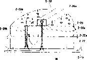
Fig. 1 is the plot plan that an embodiment of base plate processing device of copper electrolyte of the present invention is used in expression.
Fig. 2 is an airflow cardon in presentation graphs 1 base plate processing device.
Fig. 3 is an airflow cardon interregional in presentation graphs 1 base plate processing device.
Fig. 4 is the external view that Fig. 1 base plate processing device is placed in the example in the cleaning chamber.
Fig. 5 is the plot plan of another example of expression base plate processing device.
Fig. 6 is the expression base plate processing device plot plan of another example again.
Fig. 7 is the plot plan of the further example of expression base plate processing device.
Fig. 8 is the expression base plate processing device plot plan of further example again.
Fig. 9 is the still further plot plan of example again of expression base plate processing device.
Figure 10 is the schema that the base plate processing device flow process of solution and coating method of the present invention is used in expression.
Figure 11 is the skeleton diagram of expression inclined-plane/back side washing device.
Figure 12 is the longitudinal cross-section frontview of expression annealing device example.
Figure 13 is the plan cross-sectional view of Figure 12.
Figure 14 represents to be formed by plated copper the example of the process of copper wire.
Figure 15 represents still whole cross-sectional view strengths of further embodiment of base plate processing device.
Figure 16 is a plating bath mobile plating bath flow graph in expression Figure 15 base plate processing device.
Figure 17 is the cross-sectional view strength of non-plating operating period (substrate reception-transfer operation) Figure 15 whole base plate processing unit (plant).
Figure 18 be safeguard during the cross-sectional view strength of Figure 15 whole base plate processing unit (plant).
Figure 19 is illustrated in the cross-sectional view strength that concerns between shell (housing) during the substrate reception-transfer operation of Figure 15 base plate processing device, pressure ring (press ring) and substrate.
Figure 20 is the part enlarged view of Figure 19.
Figure 21 is plating and the non-plating operating period plating bath mobile figure that is illustrated in Figure 15 base plate processing device.
Figure 22 represents the amplification cross-sectional view strength of the stay cord-tractive structure (wick-drawingmechanism) of Figure 15 base plate processing device.
Figure 23 is the cross-sectional view strength of the contact point of power source (probe) of Figure 15 base plate processing device.
Figure 24 is the base plate processing device further orthographic plan of example still that plating bath of the present invention is used in expression.
Figure 25 is the cross-sectional view strength of Figure 24 along the A-A line.
Figure 26 is the substrate retaining part of Figure 24 base plate processing device and the cross-sectional view strength of cathode portion.
Figure 27 is the cross-sectional view strength of Figure 24 base plate processing device horn part.
Figure 28 is the cross-sectional view strength that Figure 24 base plate processing device removes the horn part of decapsidate.
Figure 29 is the anode of presentation graphs round substrate processing unit (plant) and the synoptic diagram of plating bath impregnating material.
Figure 30 schematically shows the structure of blind via hole part in the printed circuit board (PCB) that uses in the example 1.
Figure 31 represents to be used for the measurement point diagram of the printed circuit board (PCB) cross sectional thickness that practical measuring examples 1 is used behind the pattern plating.
Figure 32 schematically shows the structure of circuit pack in the plug-in card that uses in the example 2.
Figure 33 represents to be used for the measurement point diagram of the plug-in card cross sectional thickness that practical measuring examples 2 is used behind plating.
Figure 34 represents in the example 3 thickness measurement point figure behind the communicating pores cross-sectional configuration figure of the perforation orifice plate that uses and the plating.
Figure 35 is the cross-sectional view strength of the silicon wafer via hole inwall of use in the expression example 5.
Figure 36 is illustrated in the use-case 5 cross-sectional view strength of via hole inwall after plating bath 5 copper facing of the present invention.
Figure 37 is illustrated in the use-case 5 cross-sectional view strength of via hole inwall after plating bath 6 copper facing of the present invention.
Figure 38 is illustrated in the use-case 5 cross-sectional view strength of via hole inwall after plating bath 7 copper facing of the present invention.
Figure 39 is the cross-sectional view strength that is illustrated in the use-case 5 via hole inwall behind the relatively plating bath 1 and 2 copper facing.
Figure 40 is the cross-sectional view strength that is illustrated in the use-case 5 via hole inwall after relatively plating bath 3 copper facing.
Embodiment
Copper electrolyte of the present invention is characterised in that the reaction condensate that comprises aminated compounds and glycidyl ether and/or this reaction condensate quaternary ammonium derivative component as necessity.This component suppresses copper and deposits to the surface and go up or protuberate, and the recess of plated substrate preferably.Specifically, this component plays a part additive to filling recess with copper.
Because reaction condensate only is subjected to the influence of bath flow rate and stir speed (S.S.) slightly, and be stable in plating bath, so can obtain to have the good copper coating of height lamination reliability and electroconductibility.In addition, because reaction condensate can be adding than the more amount of conventional additive and to obtain higher concentration, so that the analysis of copper electrolyte and control become is easy.
Although its details is also also unintelligible, this specific character of reaction condensate is considered to because the structure of reaction condensate causes.Even nitrogen groups not by cationization, but is thought reaction condensate lotus positive electricity faintly in plating bath in the condenses molecule.The quaternary ammonium derivative of condenses has also been thought by cationization, therefore shows the effect similar to reaction condensate.
The example that is used as the amine of one of reaction condensate starting material comprises quadrol, trimethyl diamine, propylene diamine, hexanediamine, N-benzene quadrol, dimethylamine, diethanolamine, diethylaminopropylamine or the like.
The example that is used as the glycidyl ether of one of reaction condensate starting material comprises phenyl glycidyl ether, glycidyl allyl ether, o-phenyl benzene glycidyl ether, butylglycidyl ether, glycidyl methyl ether, glycidyl p-nitro phenylate, glycidyl isopropyl benzene ether, glycidyl methoxy phenylate, glycidyl 2-ethylbenzene ether, ethylene glycol diglycidylether, polyethyleneglycol diglycidylether, glycerine glycidyl ether, Polyglycerine polyglycidyl ether or the like.
As the reaction condensate of amine compound and glycidyl ether or the specific examples of its quaternary ammonium derivative (hereinafter being called " reaction condensate etc. " sometimes), provided the compound shown in following structural formula (I)-(IV):

N represents the integer of 1-10 in the formula, and R
1And R
2Represent hydrogen atom, replacement or unsubstituted alkyl or replacement or unsubstituted thiazolinyl independently with 1~10 carbon atom.
N represents the integer of 1-10, R in the formula
3To R
5Represent hydrogen atom, replacement or unsubstituted alkyl or replacement or unsubstituted thiazolinyl independently, and X-represents halide-ions with 1~10 carbon atom.

N represents the integer of 1-10 in the formula, and R
6To R
9Represent hydrogen atom, replacement or unsubstituted alkyl or replacement or unsubstituted thiazolinyl independently with 1~10 carbon atom.
N represents the integer of 1-10, R in the formula
10To R
15Represent hydrogen atom, replacement or unsubstituted alkyl or replacement or unsubstituted thiazolinyl independently, and X-represents halide-ions with 1~10 carbon atom.
Provide the compound of following structure formula V shown in (XX) as concrete preferred embodiments such as reaction condensates:


These reaction condensates etc. can perhaps prepare by reaction condensate is changed into quaternary ammonium salt alternatively from above-described amine and glycidyl ether by traditional reaction-condensation reaction.For example, can use following method of condensing.
Specifically, the compound of structure formula V can be by dissolving ethylene glycol diglycidylether, add 50% about 30 minutes of dimethylamine agueous solution, stirring at room mixture and condensation under reduced pressure and dry gained reaction mixture in this solution in water.
The compound (quaternary ammonium derivative) of structural formula (IX) can extremely reflux and condensation under reduced pressure and dry gained reaction mixture by structure formula V compound, adding chlorallylene, the heated mixt that obtains above the dissolving in acetone and water.The reaction condensate of other structural formula etc. also can obtain according to similar methods.These reaction condensates etc. can be purchased, for example trade mark be KB-12 (Goo Chemical Co., Ltd.).The also product that can use these to be purchased.
The reaction condensate of these aminated compoundss and glycidyl ether or the quaternary ammonium derivative of this reaction condensate can use separately or two or more are used in combination.Component concentrations is 10~1 of a copper electrolyte, 000mg/L, and be preferably 50~500mg/L.
Any copper compound that uses in the traditional copper plating bath can need not any specific qualification as the copper source in the copper electrolyte of the present invention.Specific examples comprises the organic acid mantoquita of alkanol sulfonic acids copper, for example neutralized verdigris, Cuprocitrol and cupric tartrate of alkylsulphonic acid copper, for example hydroxyethylsulfonic acid copper and the hydroxypropyl sulfonic acid copper of copper sulfate, cupric oxide, cupric chloride, copper carbonate, cupric pyrophosphate, for example copper methane sulfonate and propanesulfonic acid copper, and the salt of copper compound.These copper compounds can use separately or two or more are used in combination.
The concentration of cupric ion is 25~75g/L of copper electrolyte, and is preferably 35~60g/L.
Although metallic copper is the main ingredient of copper electrolyte of the present invention, but plating bath can comprise other metal, for example Ge, Fe, In, Mn, Mo, Ni, Co, Pb, Pd, Pt, Re, S, Ti, W, Cd, Cr, Zn, Sn, Ag, As, Au, Bi, Rh, Ru and Ir.
In copper electrolyte of the present invention, can use any organic acid and mineral acid, and without any specific restriction, as long as this organic or inorganic acid can dissolved copper.Concrete preferred embodiment comprises sulfuric acid, alkansulfonic acid, for example methylsulfonic acid and propanesulfonic acid, alkanol sulfonic acids, for example hydroxyethylsulfonic acid and hydroxypropyl sulfonic acid, and organic acid, for example citric acid, tartrate and formic acid.These organic acids and mineral acid can use separately or two or more are used in combination.Keeping copper electrolyte of the present invention is desirable for acidity.
The concentration of organic acid or mineral acid is preferably 10~200g/L of copper electrolyte, and more preferably is 20~100g/L.
Copper electrolyte of the present invention can further comprise sulfoalkyl sulfonic acid or its salt, two sulphur organic acid and dithiocarbamic acid derivative.These compounds are additives of so-called carrier component or brightener.Concrete example comprises following compound.
(1) sulfoalkyl sulfonic acid or its salt of structural formula (XXI) below:
HS-L
1-SO
3M
1 (XXI)
In the formula, L
1Expression has the saturated or undersaturated alkylidene group and the M of 1~18 carbon atom
1Expression hydrogen atom or basic metal.
(2) two sulphur organic acids of structural formula (XXII) below:
X
1-L
2-S-S-L
3-Y
1 (XXII)
In the formula, X
1And Y
1Expression sulfuric ester or phosphoric acid ester remnants, and L
2And L
3Expression has the saturated or undersaturated alkylidene group of 1~18 carbon atom.
(3) the dithiocarbamic acid derivative of structural formula (XXIII) below:

In the formula, R
3And R
4Expression hydrogen atom or have the low alkyl group of 1~3 carbon atom, L
4Expression have 3~6 carbon atoms alkylidene group, and X
2Expression sulfuric ester or phosphoric acid ester remnants.
These components can use separately or two or more are used in combination.These component concentrations are preferably 0.1~200mg/L of copper electrolyte, and more preferably are 0.3~20mg/L.
Except said components, in copper electrolyte of the present invention, preferably can contain chlorion, its concentration is calculated with chlorine and is preferably 0.01~100mg/L, and more preferably is 10~60mg/L.
Except said components, copper electrolyte of the present invention can comprise the polyethers that uses usually in copper electrolyte, concrete polymkeric substance is polyoxyethylene glycol for example, polypropylene glycol, Pluronic (pluronic) type tensio-active agent, tetronic acid (tetronic) type tensio-active agent, polyoxyethylene glycol-glyceryl ether, polyoxyethylene glycol-dialkyl ether, and be used to reduce capillary wetting agent, the polyalkyleneimine of so-called levelling agent and alkyl imidazoline compound, the alkyl imidazoline compound, auramine and derivative thereof, phthalocyanine compound, organic dye that Jia Nasi (Janus) is green or the like for example.
Copper electrolyte of the present invention can prepare according to traditional method.The details of method can be considered the component in the composition and measure suitably and determine.
The preferred process that uses above-mentioned copper electrolyte to implement solution and coating method of the present invention is described now.
Copper electrolyte of the present invention use to as if having a substrate of conductive film pattern.Substrate can have the blind via hole of about 30~200 μ m of diameter and about 20~100 μ m of the degree of depth (thickness of resin layer).Except via hole, substrate can comprise the ditch (or groove) that is used for little circuit or stretch into the interior communicating pores of substrate.
The copper coating that solution and coating method of the present invention can be guaranteed to have on the semiconductor substrate of silicon wafer for example and the surface on the printed circuit board (PCB) of small schematic circuit has high electroconductibility.Small schematic circuit on the substrate forms from very little ditch and hole, and ditch and hole are filled with metallic copper circuitry lines is provided.As an example of the circuit card that uses in the solution and coating method of the present invention, provided and had wide about 0.05~10 μ m, the substrate of dark about 0.4~1 μ m ditch.
The specific examples of this substrate is a printing plate, for example is used for directly installing the base plate for packaging of IC carries chips, directly the silicon wafer of LSI etc. and be used to silicon wafer substrate of producing semi-conductor chip etc. is installed.
If desired, substrate can be by traditional method pre-treatment.When substrate was the silicon base of for example silicon wafer etc., preprocessing process preferably formed the blocking layer of Ta, TaN, TiN, WN, SiTiN, CoWP, CoWB etc.
In solution and coating method of the present invention, before copper facing, to implement electroconductibility and handle, it is the metal seed layer that is formed for providing electric charge to substrate.Electroconductibility is handled and can be implemented by any traditional electroconductibility treatment process, for example by electroless plating, use direct solution and coating method, sputter, the vapour deposition of carbon or palladium, the perhaps chemical vapor deposition (CVD) metal or the carbon coating processing of carrying out.Electroconductibility is handled and is being carried out on substrate behind the patterning usually, but patterning also can carry out on substrate after electroconductibility is handled.
Then, the substrate after electroconductibility is handled comes plated copper with copper electrolyte.Copper electrolyte of the present invention prepares by traditional method.Use the plating of copper electrolyte also can under the condition identical, implement with traditional vitriol plating.Concrete condition can be bathe temperature between 23~27 ℃ and cathode current density be about 1~3A/dm
2Preferably stir by ventilation or circulation with pump.
Plating has the patterned substrate of blind via hole and comes the required time of completely filled via hole to change according to the diameter and the degree of depth of via hole with above-mentioned the inventive method.For example, the via hole of diameter 100 μ m and the degree of depth 50 μ m is at about 2A/dm
2Cathode current density under may need about 60 minutes plating.Operate the coating of the about 20 μ m of (except via region) generation thickness from the teeth outwards by plating.
Make under the substrate situation of semi-conductive silicon wafer, for example being used at about 2A/dm
2Cathode current density under plating be enough to for example about 0.1~0.5 μ m of diameter of completely filled, the via hole of about 0.5~1 μ m of the degree of depth or small circuit groove in about 150 seconds.In the case, operate the coating of the about 1 μ m of (except via region) generation thickness from the teeth outwards by plating.
Except controlled on a large scale additive concentration, a prominent feature of the present invention is to use the common electrical chemical apparatus that is purchased to utilize cyclic voltammetric desorb (CVS) method can easily analyze all binder components.This feature allows with the concentration of stable manner control additive and guarantees high quality and high yield, causes significant cost to descend.
Above-mentioned solution and coating method of the present invention is applicable to and uses many plating processes and device.As the device example of advantageously implementing the inventive method, several base plate processing devices that have the plating processing part will be described below.
Fig. 1 represents to be used to implement the plot plan of an embodiment of the base plate processing device that has the plating processing part of solution and coating method of the present invention.As shown in the figure, base plate processing device has and is used to transmit importing-spread out of district 520 into, implementing processing of the substrate box that includes semiconductor substrate, comprise the processing district 530 of plating processing, and be used for washing-drying zone 540 at processing after scouring and drying of semiconductor substrate.Washing-drying zone 540 is placed in and imports into-spread out of between district 520 and the processing district 530.Importing into-spreading out of between district 520 and the washing-drying zone 540 provides subregion 521, and provides subregion 523 between washing-drying zone 540 and processing district 530.
Semiconductor board circuit base plate processing unit (plant) with this configuration is installed in the cleaning chamber.The pressure of setting each district makes it to satisfy relation of plane down: (importing-spread out of the pressure in district 520 into)>(pressure of washing-drying zone 540)>(pressure of processing district 530).
In addition, the pressure that the pressure that imports-spread out of district 520 into is lower than cleaning chamber is set.Under this mode, air is 530 flow direction washing-drying zones 540 from the processing district, flow to from washing-drying zone 540 and import-spread out of district 520 into, and stop it to flow to cleaning chamber from importing-spread out of district 520 into.
Importing into-spreading out of in the district 520 provides stowage unit 520a and unloading mechanism 520b, is used to hold the substrate box that semiconductor substrate is housed.Washing part 541 and drying nest 542 are provided in washing-drying zone 540, and each is a pair of, is used for the aftertreatment after the plating process.In washing-drying zone 540, also provide a transport section (transporting mechanical manipulator) 543 to transmit semiconductor substrate.The tip have the pencil-type washer of sponge or have sponge the roll-type washer can as the washing part 541.Semiconductor substrate moisture eliminator dehydrated by high speed rotating and dry type can be used as drying nest 542.
In processing district 530, be equipped with that to be used for the plating container 532 that the semiconductor substrate plating operates pretreated pretreating containers 531 and be used for the operation of copper plating (be plater of the present invention, can be applicable to the device of plating in the following base plate processing device), and the transport section (transporting mechanical manipulator) 533 that is used to transmit semiconductor substrate.
Fig. 2 represents air flowing in base plate processing device.In washing-drying zone 540, fresh air enters from the outside by pipeline 546, is forced through in high performance strainer 544 accesss to plant and as the clean air that flows downward from ceiling 540a by fan and is supplied to washing part 541 and drying nest 542.The clean air of most of supply returns ceiling 540a through a circulating line 545 from floor 540b, is forced through in high performance strainer 544 accesss to plant by fan, and is recirculated into washing-drying zone 540.The part air is discharged from washing part 541 and drying nest 542 by conduit 552.
Although processing district 530 is humid zones, do not allow particle to be attached on the surface of semiconductor substrate.Therefore, air has been forced through high performance strainer 533 and enters by fan after, can stop particle to be attached on the semiconductor substrate by to processing district 530, introducing the clean air that flows downward from ceiling 530a.
But,, then must provide and emit the air of enormous amount if whole clean airs is all taken from external source.For this reason, only be used to keep the little air that room pressure is lower than barometric point, and the air that major part flows downward is through recycling pipe 534,535 circulation-supplied by conduit 553 discharges.
Because the round-robin air can comprise the moisture and the gas of liquid chemical medicine after by processing district 530, thus air is passed through scrubber 536 and mist separator 537,538, thus dry-off moisture and gas.Under this mode, the air that does not contain liquid chemical medicine moisture and gas is returned the recycling pipe 534 on the ceiling 530a limit.Then, circulation enters processing district 530 by high performance strainer 533 and as clean air to force air again through fan.
Part is discharged to the external world from the air that floor 530b enters processing district 530 by conduit 553.Under this mode, the air that contains liquid chemical medicine moisture and gas is discharged to the external world by conduit 553.Be equivalent to the pressure that the fresh air of discharging gas keeps in the processing district 530 from its amounts of conduit 539 supply of ceiling 530a and be lower than barometric point.
The pressure that setting is imported into-spread out of in district 520, washing-drying zone 540 and the processing district 530 makes it to satisfy relation of plane down: (importing-spread out of the pressure in district 520 into)>(pressure of washing-drying zone 540)>(pressure of processing district 530).
Therefore, when the baffle plate (see figure 2) was being opened, air flowed on direction as shown in Figure 3, promptly from importing-spread out of district 520 into to washing-drying zone 540, arrived processing district 530 again.As shown in Figure 4, waste gas is collected in the waste pipe 554 by conduit 552,553.
Fig. 4 is the appearing diagram that expression is placed in the base plate processing device in the cleaning chamber.Import-spread out of district's 520 one sides that box delivery port 555 and switchboard 556 are installed into and be exposed to the highly workspace 558 of cleaning, and separate by the dividing wall in the cleaning chamber 557.Another side is mounted with the highly use district 559 of cleaning.
Import into-spread out of between district 520 and the processing district 530 because washing-drying zone 540 is installed in, and dividing wall is installed in and imports-spread out of district 520 and 540 of washing-drying zones into, and 530 of washing-drying zone 540 and processing districts, so be conveyed into the base plate processing device of making circuit from workspace 558 by box delivery port 555 semiconductor substrates, and in base plate processing device, process, and after plating, washing and drying, output to workspace 558.Therefore, do not have particle to be attached on the semi-conductive surface, and the workspace 558 of cleaning chamber camber cleaning can not polluted by the moisture of particle, liquid chemical medicine and washing.
Although Fig. 1 and Fig. 2 represent to have the embodiment of the base plate processing device that imports-spread out of district 520, washing-drying zone 540 and processing district 530 into, but the district of a band CMP device can be provided near processing district 530 or processing district 530, and make washing-drying zone 540 in the processing district 530 in this CMP of having device district with import into-spread out of and distinguish between 520.Unique necessary be that the base plate processing device of making circuit can be accepted semiconductor substrate and the semiconductor substrate of conveying plating under washing and drying conditions in drying conditions.
Illustrated the circuit pack that the substrate and the Political Bureau are limited to semiconductor substrate and are not limited to form by the part of plating operation processing in the above embodiments on substrate surface although make the base plate processing device of circuit semiconductor substrate.
Fig. 5 represents to make the plot plan of another base plate processing device of circuit semiconductor substrate.As shown in the figure, the base plate processing device of making the circuit semiconductor substrate have be used to import into semiconductor substrate import part 601 into, be used for the copper facing operation copper facing container 602, be used to wash with water the washing container 603 of operation, 604, be used for CMP part 605, washing container 606,607, the drying receptacle 608 of chemically machinery polished (CMP) and be used to transmit the semiconductor substrate that formed line layer spread out of part 609.Be used for transmitting semiconductor substrate is arranged to the base plate processing device that forms manufacturing circuit semiconductor substrate to the base plate transfer device (not shown) of these parts and container a device.
In the above in Pei Zhi the base plate processing device, the semiconductor substrate that does not form line layer above is from being arranged in the substrate box 601-1 that imports part 601 into and sending and import into copper facing container 602.In copper facing container 602, on the surface of the semiconductor substrate W that comprises the circuit pack of forming by circuit groove and circuit hole (contact hole), form copper coating.
The semiconductor substrate W that has formed copper coating in above-mentioned copper facing container 602 is conveyed into by base plate transfer device in washing container 603 and the washing container 604, washes with water.After the washing, semiconductor substrate W imports CMP part 605 into by base plate transfer device, removes the plated copper layer except the part that forms circuit groove and circuit hole on the semiconductor substrate W surface there.
Next, except the copper layer that forms the circuit pack of forming by circuit groove and circuit hole, having removed does not need the semiconductor substrate of plated copper layer W to be used semiconductor-based substrate transfer device to deliver in washing container 606 and the washing container 607, wash semiconductor substrate W there with water.Semiconductor substrate W after drying washes with water in drying receptacle 608 then.Exsiccant semiconductor substrate W is stored among the substrate box 609-1 that spreads out of part 609 as the semiconductor substrate of finishing line layer formation.
Fig. 6 represents to make the plot plan of another base plate processing device again of circuit semiconductor substrate.Base plate processing device shown in Figure 6 is different from device shown in Figure 5; because additional covering plating container 612, the CMP part 615 that comprises copper facing container 602, is used on the copper film of plating, forming protective layer of the device of Fig. 6; and washing container 613; 614, formed the device that comprises these extentions and container.
In the base plate processing device of above-mentioned configuration, copper coating forms on the surface of the semiconductor substrate W that comprises the circuit pack of being made up of circuit groove and circuit hole (contact hole).Then, except the part that forms circuit groove and circuit hole, remove the lip-deep plated copper layer of semiconductor substrate W in CMP part 605.
Then, except the part that forms circuit groove and circuit hole, the semiconductor substrate W that has removed the plated copper layer is sent in the washing container 610, washes semiconductor substrate W there with water.In order to carry out following tectum plating, substrate is being used for pretreated pretreating containers 611 processing then.Pretreated semiconductor substrate W is sent to and covers in the plating container 612, forms protective membrane there on the surface of the plated copper layer that forms circuit pack.For instance, Ni-B electroless plating container can be used to form protective membrane.After having formed protective membrane, washing semiconductor substrate W in washing container 606 and washing container 607, and dry in drying receptacle 608.
Then, in CMP part 615, ground and polished on the surface of the protective membrane that forms on the copper coating.Washing and in drying receptacle 608 after the drying in washing container 613, semiconductor substrate W is stored among the substrate box 609-1 that spreads out of part 609.
Fig. 7 represents the still plot plan of another base plate processing device.This semiconductor substrate processing unit (plant) has loading-unloading part 701, copper plating device 702, first mechanical manipulator 703, the 3rd washer 704, reversing device 705, reversing device 706, second washer 707, second mechanical manipulator 708, first washer 709, first polishing machine 710 and second polishing machine 711.The measurer for thickness 713 that is used at the thickness of coating measuring apparatus 712 of plating fore-and-aft survey thickness and is used to measure polishing after drying semiconductor substrate W thickness is installed near first mechanical manipulator 703.
First polishing machine 710 (milling apparatus) is equipped with polishing block 710-1, collar 710-2, collar lid 710-3, film thickness measurement device 710-4 and pushing device 710-5.Second polishing machine 711 (milling apparatus) is equipped with polishing block 711-1, collar 711-2, collar lid 711-3, film thickness measurement device 711-4 and pushing device 711-5.
The box 701-1 that comprises the semiconductor substrate W that forms contact hole and circuit groove is placed in the loading station of loading and unloading part 701.First mechanical manipulator 703 takes out semiconductor substrate W and sends in the copper plating device 702 that is used to form the copper coating film from box 701-1.In this case, the thickness of seed layer is measured by the thickness of coating measuring apparatus 712 that is used at plating fore-and-aft survey thickness.The copper facing operation comprises the wetting ability processing and the formation copper film subsequently on semiconductor substrate W surface.After forming the copper coating film, rinsing or washing substrate in copper plating device 702.If free, semiconductor substrate W can be dried.
When taking out semiconductor substrate W from installing 702 with first mechanical manipulator 703, the copper film thickness of plating is measured by the thickness of coating measuring apparatus 712 that is used at plating fore-and-aft survey thickness.In the recording unit (not shown), write down the record data of the result of measurement, and be used to judge the abnormal condition of copper plating device 702 as semiconductor substrate W.After measuring thickness, first mechanical manipulator 703 is sent into semiconductor substrate W in the reversing device 705, and W is reversed by reversing device semiconductor substrate, makes the surface that is coated with copper downward.The serial or parallel connection pattern can be applied to the polishing operation of first polishing machine 710 and second polishing machine 711.The following description of the grinding operation of series model.
The grinding operation of series model comprises the elementary polishing of first polishing machine 710 and the secondary polishing of second people's polishing machine 711.Second mechanical manipulator 708 takes out semiconductor substrate W and puts into the pushing device 710-5 of polishing machine 710 from reversing device 705.The surface that collar 710-2 holds the semiconductor substrate W on the pushing device 710-5 and makes semiconductor substrate W be coated with copper contacts and is pressed onto above it with the glazed surface of grinding stage 710-1, carries out the polishing first time thus.The copper film of plating is polished basically in polishing for the first time.The glazed surface of grinding stage 710-1 is by the polyurathamc pad of for example IC1000, and the material of perhaps wherein fixing or be filled with polishing particles constitutes.The copper film of plating is ground by the relative movement of glazed surface and semiconductor substrate W.
Behind the copper film that grinds plating, semiconductor substrate W turns back on the pushing device 710-5 with collar 710-2.Second mechanical manipulator 708 takes out semiconductor substrate W and puts into first washer 709.In this case, liquid chemical reagent can be sprayed onto on the surface or the back side of the semiconductor substrate W on the pushing device 710-5, thereby removes degranulation or particle can not be adhered to more.
After with first washer 709 washings, second mechanical manipulator 708 taking-up semiconductor substrate W also is put on the pushing device 711-5 of second polishing machine 711.The surface that collar 711-2 holds the semiconductor substrate W on the pushing device 711-5 and makes semiconductor substrate W have the blocking layer of formation contacts and is pressed onto above it with the glazed surface of polishing block 711-1, carries out the polishing second time thus.The blocking layer is polished in polishing for the second time.In some cases, copper film that is not polished in elementary polishing and oxide film also are polished.
The lapped face of grinding stage 711-1 is by the polyurathamc pad of for example IC1000, and the material of perhaps wherein fixing or be filled with polishing particles constitutes.The copper film of plating is polished by the relative movement of glazed surface and semiconductor substrate W.In this case, silicon-dioxide, aluminum oxide, cerium dioxide etc. can be used as polishing particles or slurry.Type adjustment liquid chemical reagent according to film.
The end of polishing operation for the second time detects (end operation when thickness becomes 0) by the thickness that uses the optical type film thickness measurement device to measure the blocking layer, perhaps detects the insulation layer that comprises SiO2 by the surface and determines.In order to measure the thickness of sull, installation has the film thickness measurement device 711-4 of image processing function near polishing block 711-1.The result stores as the operation record of semiconductor substrate W, is used to perhaps judge whether semiconductor substrate W needs to be conveyed into next step behind second polishing.When finding that semiconductor substrate W does not reach the terminal point of second polishing, substrate can be polished once more.If when finding the polished preset value that surpasses any abnormal condition of semiconductor substrate W, end the polishing operation of base plate processing device, prevent the increase of substandard products quantity.
After the second polishing operation, semiconductor substrate W is sent on the pushing device 711-5 with collar 711-2.The semiconductor substrate W that uses second mechanical manipulator 708 to take out on the pushing device 711-5.In this case, liquid chemical reagent can be sprayed onto on the surface or the back side of the semiconductor substrate W on the pushing device 711-5, thereby removes degranulation or particle can not be adhered to more.
Second mechanical manipulator 708 delivered to semiconductor substrate W in second washer 707, there washing semi-conductor substrate W.Second washer 707 has identical configuration with first washer 709.Clean the surface of semiconductor substrate W in washing soln with the PVA sponge, washing soln prepares thereby remove the particulate method by add tensio-active agent, sequestrant and pH regulator agent in pure water.The copper that the back side of semiconductor substrate W uses the extensive chemical solution-treated of for example DHF that injects from nozzle to come etching to scatter.If the problem that does not have copper to scatter, the back side can use identical chemical solution to clean clean surface with PVA sponge volume.
Behind washing operation, second mechanical manipulator 708 takes out semiconductor substrate W and puts into reversing device 706, reversing semiconductor substrate W.First mechanical manipulator 703 takes out inverse semiconductor substrate W and puts into the 3rd washer 704 then.In the 3rd washer, strong sound wave (mega-sonic) water that is excited by ultrasonic vibration is projected onto washing semi-conductor substrate W on the surface of semiconductor substrate W.Both select a ground, and the surface of semiconductor substrate W can use washing soln to wash with known pencil-type sponge, and washing soln prepares thereby remove the particulate method by add tensio-active agent, sequestrant and pH regulator agent in pure water.Semiconductor substrate W is by the method drying of Rotary drying then.
When near the measurer for thickness 711-4 use is installed in polishing block 711-1 measured thickness, semiconductor substrate W was placed in the box that is placed on the unloading mouth that loads and unloads 701 parts.
Fig. 8 represents the still plane device figure of another base plate processing device.This base plate processing device is different from base plate processing device shown in Figure 7, replaces copper plating device shown in Figure 7 702 because it is equipped with tectum plater 750.
The box 701-1 that comprises the semiconductor substrate W that has the plating copper film is placed on the loading and unloading part 701.From box 701-1, take out semiconductor substrate W and deliver to first polishing machine 710 or second polishing machine 711 on, the surface of grinding copper film there.After the grinding, semiconductor substrate W is sent to washing in first washer 709.
Washed semiconductor substrate W is sent in the tectum plater 750 in first washer 709, forms protective membrane on the surface of plating copper film, thereby stops latter's oxidation in atmosphere.The semiconductor substrate W that is coated with protective membrane delivers to from tectum plater 750 in second washer 707 by second mechanical manipulator 708, there with pure water or deionized water wash semiconductor substrate W.After the washing, semiconductor substrate W turns back among the box 701-1 that is placed on the loading and unloading part 701.
Fig. 9 represents the still plane device figure of another base plate processing device.This base plate processing device is different from base plate processing device shown in Figure 8, and plater 751 replaces first washer 709 shown in Figure 8 because it is equipped with annealing.
By first polishing machine 710 or second polishing machine 711 grind and in second washer 707 washed semiconductor substrate W be sent in the tectum plater 750, on the surface of plating copper film, form protective membrane.The semiconductor substrate W that is coated with protective membrane delivers to from tectum plater 750 in the 3rd washer 704 by first mechanical manipulator 703, there washing semi-conductor substrate W.
Washed semiconductor substrate W is sent to annealing in the annealing device 751 in first washer 709.Annealing changes into alloy with the copper of plating and increases the resistance of electronic migration.Semiconductor substrate W after the annealing delivers to from annealing device 751 in second washer 707, there with pure water or deionized water wash.After the washing, semiconductor substrate W turns back among the box 701-1 that is placed on the loading and unloading part 701.
Figure 10 is the schema of work flow in the expression base plate processing device.Each step will be described according to schema in the device.Be placed in first calibrator-thickness measurement equipment (aligner-thickness measurer) 841 with the semiconductor substrate W that takes out the box 820a of first mechanical manipulator 831 on being placed on handler 820, the surface of plating to make progress.In this case, in order to determine the location criteria point of film thickness measuring, the indentation of calibration film thickness measuring before the thickness data of semiconductor substrate before obtaining the plating copper film.
By first mechanical manipulator 831 semiconductor substrate W being delivered to the blocking layer then forms in the device 811.It is electroless plating Ru forms the blocking layer on semiconductor substrate devices that the blocking layer forms device 811.Form the Ru film as stoping copper film to diffuse into the semiconductor device interlayer dielectic (for example by SiO
2The film that forms) film in.To deliver on first calibrator-thickness measurement equipment 841 from washing and drying step progressive semiconductor substrate W by first mechanical manipulator 831, measure the thickness of semiconductor substrate, i.e. the thickness on blocking layer.
After measuring thickness, second mechanical manipulator 832 is transported to the device 812 that forms the seed layer with semiconductor substrate, forms the seed layer by electroless copper on the blocking layer.Before being transported to dipping plater 813, will deliver on second calibrator-thickness measurement equipment 842 from washing and drying step progressive semiconductor substrate W by second mechanical manipulator 832.The indentation of copper coating is by 842 calibrations of second calibrator-thickness measurement equipment.In this case, before copper facing, can measure the thickness of semiconductor substrate if desired once more.
Behind the calibration indentation, semiconductor substrate is delivered in the copper-plated plater 813 by the 3rd mechanical manipulator 833.To deliver to inclined-plane/back side washing device 816 from washing and drying step progressive semiconductor substrate W by the 3rd mechanical manipulator 833, remove the unwanted copper film in semiconductor substrate end (seed layer).In inclined-plane/back side washing device 816, the copper that is attached to the semiconductor substrate back side is washed on etching inclined-plane and use chemical solution in the prior specified time off as hydrofluoric acid.In this case, before semiconductor substrate advances in inclined-plane/back side washing device 816, measure the thickness of semiconductor substrate with second calibrator-thickness measurement equipment 842.The etching period on inclined-plane can change arbitrarily according to the gained copper film thickness that plating forms.Wanting etched zone by the inclined-plane etching is the periphery of substrate, and the there does not form circuit, even formed any circuit also not as chip.Chamfered portion is included in this zone.
By the 3rd mechanical manipulator 833 will wash and drying step after from inclined-plane/back side washing device 816 progressive semiconductor substrate W deliver on the substrate reversing machine 843, and reversing faces down the surface of plating, then is sent in the annealing device 814 by the 4th mechanical manipulator 834 and stablizes circuit.Before or after anneal, semiconductor substrate is sent on second calibrator-thickness measurement equipment 842, measures the thickness of the copper film that forms on semiconductor substrate.After this, semiconductor substrate is delivered on first polishing machine 821 polish copper layer and seed layer by the 4th mechanical manipulator 834.
Optionally abrasive grain comprises that the fixed-abrasive particle of guaranteeing flat surfaces can be used for polishing, stops the surface to become spill.After in first polishing machine, finishing grinding, semiconductor substrate is delivered to washing in first washing device 815 by the 4th mechanical manipulator 834.In washing operation, place approximately and the cylinder of semiconductor substrate equal length on the two sides (surface and the back side) of semiconductor substrate.When rotation semiconductor substrate and cylinder and injection pure water or deionized water, clean semiconductor substrate.
After washing is finished for the first time, semiconductor substrate is delivered to the blocking layer that forms on the polishing semiconductor substrate on second polishing machine 822 by the 4th mechanical manipulator 834.Any optional abrasive grain comprises that the fixing polishing particle of guaranteeing flat surfaces can be used for grinding, and stops the surface to become spill.After in second polishing machine, finishing grinding, by the 4th mechanical manipulator 834 semiconductor substrate is advanced in first washing device 815 once more and to clean semiconductor substrate.After the washing, by the 4th mechanical manipulator 834 semiconductor substrate is advanced on second substrate reversing device 844, and the surface that reversing makes plating puts it on the temporary base platform 845 by the 3rd mechanical manipulator 833 then towards last.
By second mechanical manipulator 832 semiconductor substrate is delivered to the tectum plater 817 from temporary base platform 845, thereby stoped copper oxidation in atmosphere at copper coating surface nickel-boron.The semiconductor substrate that will cover protective membrane by second mechanical manipulator 832 is delivered to the thickness of measuring copper film in the 3rd the film thickness measuring device 846 from tectum plater 817.Then, will deliver to before the semiconductor substrate in second washing device 818 by first mechanical manipulator 831, thereby with pure water or deionized water wash semiconductor substrate.After the washing, semiconductor substrate is sent back among the box 820a that is placed on the loading and unloading part 820 by first mechanical manipulator 831.
Calibrator-thickness measurement equipment 841 and calibrator-thickness measurement equipment 842 are determined the position of substrate indentation and are measured thickness.
In inclined-plane/back side washing device 816, (inclined-plane) etch copper and wash the back side simultaneously from the edge.The growth of the copper film of circuit pack control natural oxidation that in addition, can be on semiconductor substrate surface.Figure 11 represents the skeleton diagram of inclined-plane/back side washing device 816.As shown in figure 11, inclined-plane/back side washing device 816 is equipped with substrate and supports part 922 in having the cylindrical waterproof cover of bottom, the level of being used for is propped up carried base board W and is made its high speed rotating, use a plurality of spin chucks 921 that are installed in the cylinder periphery to make the upper surface of substrate W simultaneously towards last, also be equipped with to be installed in and support 922 of parts to be loaded in the central nozzle 924 on the ectocentral substrate W in substrate W surface, and be installed in substrate W peripheral upper edges nozzle 926 by substrate.Central nozzle 924 and edge nozzle 926 all are equipped with downward nozzle.Also be equipped with the back side nozzle 928 that has upward nozzle in the nearly centre in the back side of substrate W.Edge nozzle 926 is configured in the horizontal and vertical directions can be with respect to substrate W free movement.
The method of using this washing device washing is described now.At first, prop up the semiconductor substrate W that carries by rotary chuck 921 levels by substrate support part 922 and support that with substrate part 922 horizontally rotates.In this case, from the surface applied acidic solution of 924 pairs of nearly centre of substrate W of central nozzle.Non-oxidizing acid can be used as acidic solution.Example comprises hydrofluoric acid, hydrochloric acid, sulfuric acid, citric acid, oxalic acid or the like.On the other hand, from edge nozzle 926 continuously or off and on to using oxidizing agent solution around the substrate W.Ozone water solution, superoxol, salpeter solution, chlorine bleach liquor can be used as oxidizing agent solution.
The quick oxidations of oxidized agent solution such as copper film that in the side cut width C zone of semiconductor substrate W periphery, form with edge, removed by acidic solution etching and dissolving simultaneously, and expand to whole surface by this operation from central nozzle 924 supplies.Can produce more precipitous etching side, the resulting side of the solution that is pre-mixed than use at substrate peripheral blending oxidizing agent and acidic solution by this way.The etching speed of copper is determined according to the concentration of used solution.Any oxide film of the copper of formation is immediately removed by acidic solution and the rotation by substrate expands on the whole surface in the substrate surface circuit forms the district.Therefore, the oxide film of this copper can not accumulate.Behind the acidic solution that stops using from central nozzle 924, adhering to of copper can be controlled by being exposed to lip-deep silicon oxide by stopping supplying oxidizing agent solutions from edge nozzle 926.
On the other hand, the etching solution of oxidizing agent solution and silicon oxide film is by parallel or alternately be applied to the central authorities of substrate back from back side nozzle 928.Be attached to metallic copper on the semiconductor substrate back side etc. with oxidized dose of oxidation of silicon substrate, and use the etching solution etching of silicon oxide film to remove.For the quantity of used chemical in the reduction process, the solution identical with the oxidizing agent solution that is used for the surface can preferably be used as oxidizing agent solution.Hydrofluoric acid can be as the etching solution of silicon oxide film.In this case, from reducing the angle of used chemical quantity, using hydrofluoric acid is preferred as the acidic solution that is used for the surface.If at first stop using oxygenant, can obtain hydrophobic surface; If at first stop using etchant solutions, then obtain water-wetted surface.Can regulate the back side according to the needs of subsequent disposal by this way.
In this manner, removing by substrate mugineic acid solution (etching solution) after being retained in the lip-deep metal ion of substrate W, is replaced etching solution with pure water, thereby removing etching solution.Then, be rotated drying operation.The removal of copper film copper pollutant on the removal in the side cut width C zone of semiconductor substrate W periphery and the back side can be implemented in 80 seconds simultaneously by this way in the short period of time.Although optional width inner cutting edge edge that may be in 2~5 millimeters scopes, the required time of etching is not depended on the side cut width at edge.
Behind the plating and the annealing steps before the CMP step is handled for CMP and the electrology characteristic of circuit is effective.When after the observation CMP processing and unannealed wide circuit surface (several microns), observe many be similar to defective of microcavities and the resistance increases of whole circuit.The increase of resistance is improved by annealing.Based on the fact of in the thin circuit of unannealed processing, not observing the hole, think that the degree of particle growth is relevant with annealing.Specifically, although particle is difficult to growth in thin circuit, wide circuit can allow the particulate growth.During the particle growth in anneal, believe even all be difficult to observed very little hole when fluctuating, to move upward, thereby produce the depression that forms microcavities on the online road surfaces by SEM (scanning electron microscope).As for the annealing conditions in the annealing device, when adding 2% or still less in the atmosphere of hydrogen in about 300~400 ℃ down annealing obtain the above-mentioned effect of wanting in the time of 1~5 minute.
Figure 12 and 13 expression annealing devices 814.This annealing device 814 has and is used to heat semiconductor substrate to 400 ℃ hot-plate 1004 for example, hot-plate be positioned at the chamber 1002 that has the door 1000 that is used to insert and take out semiconductor substrate W above, and be used for cooling plate 1006 by the cooling of cooling-water flowing for example semiconductor substrate W, cooling plate be installed in the top of chamber 1002 and below.In addition, vertically pass cooling plate 1006 movably at the top a plurality of lifting bolts 1008 that are used for supporting semiconductor substrate W are installed.In addition, be used for introducing the pipeline 1010 of the gas that stops oxidation and be used to discharge with position facing each other 1004 installations of hot-plate during semiconductor substrate W and annealing and introduced 1010 and flow through the pipeline 1012 of semiconductor substrate W and 1004 spatial gases of hot-plate, and hot-plate 1004 is between them.
Flow through the N that has strainer 1014a
2The N of inlet tube 1016
2Gas and flow through the H that has strainer 1014b
2The H of inlet tube 1018
2Gas mixes in mixing tank 1020.The pipeline 1010 that is used for introducing gas links to each other with the pipeline 1022 of the introducing mixed gas of crossing at mixing tank 1020 blended gas streams.
This configuration makes the semiconductor substrate W that is written in the chamber 1002 by door 1000 support by lifting bolt 1008, and lifting bolt 1008 is risen, thereby the distance that increases by 1008 of 1008 semiconductor substrate W that carry of lifting bolt and hot-plates is to for example about 0.1~1.0 millimeter.Under this condition, semiconductor substrate is heated to for example 400 ℃ by hot-plate 1004,1010 introduces anti-oxidation gas from the gas inlet tube road simultaneously, and gas flows and discharges from gas exhaust duct 1012 at semiconductor substrate W and 1004 of hot-plate.In this manner, semiconductor substrate W is annealed and can be not oxidized.Before finishing annealing, annealing operation is carried out about tens seconds to 60 seconds.The Heating temperature of substrate is selected in 100~600 ℃ scope.
After finishing annealing, the distance that reduces by 1006 of lifting bolt 1,008 1008 semiconductor substrate W that carry of minimizing lifting bolt and cooling plates is to for example about 0~0.5 millimeter.Then, made semiconductor substrate W be cooled to 100 ℃ or lower in for example about 10~60 seconds by introducing water coolant to cooling plate 1006.The refrigerative semiconductor substrate is transported to next step.
Although N
2Gas and several per-cent H
2The gas mixture of gas is used as the gas of anti-oxidation in the present embodiment, but also can use N separately
2Gas.
Another embodiment of Figure 15 to 23 expression base plate processing device of the present invention.As shown in figure 15, the main part of this base plate processing device has the subcylindrical head part that is used for fixing substrate W 47 of holding the plating process vessel 46 of plating bath 45 and being positioned at plating process vessel 46 tops.
In addition in the present embodiment, above the anode 48 of plating chamber 49, provide and have a large amount of diameters and be about for example stephanoporate steel plate 220 in 3 millimeters holes.This avoids the injury of plating bath 45 with regard to the black thin film that has stoped anode 48 surfaces to go up formation and flows out.
As shown in figure 21, plating container 50 is equipped with first plating bath outlet 57, be used for removing plating bath 45, second plating bath outlet 59 of plating chamber 49 from the bottom periphery of plating chamber 49, be used to discharge from the effusive plating bath 45 of dam 58 overflows that are positioned at plating container 50 tops, the 3rd plating bath outlet 120, be used for before overflow dam 58 discharging plating bath 45, and the opening with specific width 222 that below dam 58, provides with fixed intervals.
Discharge plating baths from the 3rd plating bath outlet 120 when this configuration allows the amount at plating operating period plating big, and allow plating bath to flow out dam 58 simultaneously and also discharge by opening 222, shown in Figure 21 (a) from the outlet 59 of second plating bath.On the other hand, when the plating amount of plating operating period supply hour, plating bath is discharged to the outside from the 3rd plating bath outlet 120, and is discharged to the outside from second plating bath outlet 59 by opening 222 simultaneously, shown in Figure 21 (b).In this manner, operation is easy to consistent with the amount of plating.
In addition, shown in Figure 21 (d), above plating bath injection nozzle 53, settle at interval with fixed to be used for the controlled liq liquid level and to connect plating chamber 49 and the communicating pores 224 of second outlet 59 along periphery.This just allows when not having the plating operation by making plating bath flow through communicating pores 224 and exporting the liquid level that 59 methods of discharging solution are controlled the plating bath liquid level from second plating bath.Communicating pores 224 also has the function that is similar to the mouth of pipe in plating operating period, therefore can control the outflow of plating bath.
As shown in figure 16, first plating bath outlet 57 links to each other with retention basin 226 by plating bath vent pipe 60a.In plating bath vent pipe 60a, provide flow regulator 61a.Second plating bath outlet the 59 and the 3rd plating bath outlet 120 connects in the plating container 50, directly is connected with retention basin 226 by plating bath vent pipe 60b then.
The plating bath 45 that enters retention basin 226 is supplied with plating bath controlling tank 40 through pump 228 from retention basin 226.Plating bath controlling tank 40 is equipped with temperature regulator 230 and is used for collecting the also plating solution analysis instrument 232 of analytic sample solution.By single pump 234 plating baths 45 are fed in the plating bath injection nozzle 53 of copper plating device 156 through filter 236 from plating bath controlling tank 40.Provide the control valve 56 that is used to keep fixedly secondary side pressure in plating bath supply-pipe 55, supply-pipe extends to the copper plating device 156 from controlling tank 40.
Now, return Figure 15, provide vertical adjustment ring 62 in the nearly surrounding zone of plating chamber 49.Vertically adjust ring 62 and make the central area on plating bath surface upwards promote and provide downward stably liquid stream, and uniform current density distributes simultaneously by the upwards liquid stream of plating bath 45 in the plating chamber 49.Not end at periphery also provides the horizontal adjustment ring 63 that is fixed on the plating container 50.
On the other hand, head part 47 is equipped with porose 94 the bottomed cylindrical shape shell 70 on lower opening and sidewall that can rotate freely, and the lower end of vertical movement has the depression bar 242 of pressure ring 240.Shown in Figure 19 and 20, in the lower end of shell 70 substrate holder 72 is installed, it is the ring that inwardly stretches out.Substrate holder 72 has sealing material 244, and it also is the ring that inwardly stretches out, and the tip on its surface protrudes upward with the shape of cone-shaped body.Negative electrode point of contact 76 is placed on the sealing material 244.In addition, provide ventilation hole 75 radially at interval with fixed on substrate holder 72, ventilation hole extends horizontally to periphery and further stretches out with being inclined upwardly.
As shown in figure 15, when the liquid level of plating bath 45 was hanged down, this configuration can maintain substrate W with absorption arm H, it is pushed shell 70 and be put on the surface of sealing material 244 of substrate holder 72, shown in Figure 19 and 20, after from shell 70, pulling out absorption arm H, reduce pressure ring 240 then.In this manner, can be by pushing its peripheral substrate W that maintains at sealing material 244 and 240 of pressure rings, thereby the bottom of hermetic sealing substrate W safely, and they maintain sealing material 244 by extruding when substrate W maintains, and substrate W and cathode electrode point of contact 76 are electrically contacted.
Referring again to Figure 15, shell 70 links to each other and is configured to the output shaft 248 of motor 246 and rotates by the driving of motor 246.Depression bar 242 is installed in appointed positions along the periphery of support 258 with annular vertical, the effect of the cylinder 252 by being equipped with guider, but it can rotate freely the lower end that twelve Earthly Branches are loaded in the slide unit 254 of vertical movement by gear 256, and guider is fixed on the supporting body 250 of motor 246.This configuration allows depression bar 242 vertical movement by the effect of cylinder 252, and integral body is rotated along with the shell 70 of support substrate W simultaneously.
But supporting body 250 uses the ball bearing 261 that rotates by motor 260 drivings to append on the slip base 262 of vertical movement.Supporting body 250 further by last shell 264 round, and be configured to by the driving of motor 260 with last shell 264 vertical movements.In addition, plating container 50 is equipped with the lower housing 257 round shell 70 in plating operating period in its surface.
This configuration allows to keep in repair in device under the condition of rising supporting body 250 and lower housing 264, as shown in figure 18.The crystal of plating bath trends towards being attached to easily on the inwall on dam 58.But,, just can stop this plating bath crystalline to adhere to if make a large amount of plating bath overflow dams 58 by rising supporting body 250 and lower housing 264.Plating container 50 integral installations have lid 50b, and it can cover the plating bath that overflows and prevent that plating bath from splashing in plating operating period.By using super water-proof material, for example (NTT Advance Technology Co. Ltd.) applies basal surface and can avoid the plating bath crystal to be attached on the basal surface of lid 50b HIREC.
In the present embodiment, provide on four points on substrate holder 72 tops of shell 70 along periphery and be used for the substrate stay cord-tractive structure 270 of tractive substrate W stay cord.Figure 22 represents the details of substrate stay cord-tractive structure 270, and it has portal trestle 272 and is fixed on the shell 70, and rack-mount preset pieces 274.Preset pieces 274 rotates freely twelve Earthly Branches by horizontal fixed pivot 276 by support 272 and is loaded in top.In addition, at shell 70 and 274 of preset piecess compression disc spring is installed.This configuration allows by compression disc spring 278 preset pieces 274 to be promoted forward around pivot 276, to such an extent as to inwardly stretch out its lower end.Upper surface 274a plays a part stopper, and forms with the bottom of the upper side 272a of support 272 and contact, so regulates the motion of preset pieces 274.The internal surface of preset pieces 274 is to make progress and outwardly directed taper 274b form.
This configuration can pulled out the stay cord of substrate in the following manner.When substrate by the absorption arm, for example transport mechanical manipulator and transfer on the shell 70 of maintenance and when being placed on the substrate holder 72, if outside preset pieces 274 turns to when the central authorities of substrate depart from substrate holder 72 central, the elastic force of opposing compression disc spring 278.Discharge substrate if for example transport the absorption arm of mechanical manipulator,, pull out the stay cord of substrate thus because the elastic force preset pieces 274 of compression disc spring 278 returns to the original position.
Figure 23 represents to be used for supplying the reinforced point of contact (probe) 77 of electric power to the cathode electrode plate 208 of cathode electrode point of contact 76.Reinforced point of contact (probe) 77 is made of piston and built-in extends to cylindrical protective body 280 on the cathode electrode plate 208, therefore reinforced point of contact (probe) the 77 protected erosions that are not subjected to plating bath.
The solution and coating method that uses base plate processing device 2-0 of the present invention is described below.At first, when substrate is transported to base plate processing device 2-0 when going up, transport the absorption arm (not shown in the diagram) of mechanical manipulator and the prone substrate W that keeps by the absorption of absorption arm by from the 94 insertion shells 70 of hole.After reducing the absorption arm, discharge vacuum suck and substrate is put on the substrate holder 72 of shell 70.Then, the absorption arm that raises, and from shell 70, pull out.Next, reduce pressure ring 240 by between the bottom of substrate holder 72 and pressure ring 240, pushing its periphery, thereby maintain substrate W.
Then, from plating bath injection nozzle 53, inject plating bath 45, simultaneously with moderate speed's rotational shell 70 and the substrate W that keeps.Be added to specified level after several seconds at plating bath 45, the speed of rotation that reduces shell 70 (for example drops to 100min
-1).Then, by making electric current flow through anode 48 and implementing electrolytic coating as the substrate of negative electrode.
After close current, reduce the amount of supply plating bath, plating bath only can be flowed out from the communicating pores 224 of fluid level controller, and controller is provided at the top of the plating bath injection nozzle 53 shown in Figure 21 (d), so the substrate of shell 70 and shell 70 maintenances is exposed to the top of plating bath liquid level.Therefore shell 70 and the position of substrate above liquid level that keep are with (500~800min for example at a high speed
-1) rotation, thereby remove plating bath by centrifugal force.After removing plating bath, stop the rotation of shell 70, to such an extent as to shell 70 can be towards specific direction.
After shell 70 stops the rotation fully, rising pressure ring 240.Then, the absorption arm that transports mechanical manipulator 28b inserts in the shell 70 from the hole 94 of shell 70, and adsorption surface faces down.Reduce the absorption arm to adsorbing the position that arm can adsorb substrate.Then, the substrate that is adsorbed by vacuum suck by the absorption arm moves to the position of 94 tops, hole of shell 70 with the absorption arm, thereby carries the substrate of absorption arms and maintenance from the hole 94 of shell 70.
Use this base plate processing device 2-0, the structure of head part 47 is simplified and minification; When the liquid level of plating bath in the plating container 46 maintains when being suitable for the plating operation, implement the plating operation, and be suitable for implementing when substrate transports operation plating bath and remove and operate and substrate transports operation when liquid level maintains.In addition, can stop the drying and the oxidation of the black thin film that on anode 48 surfaces, forms.
Another embodiment again of the base plate processing device of solution and coating method of the present invention is used in Figure 24 to 29 expression.As shown in figure 24, this base plate processing device has the substrate processing part 2-1 that is used to implement plating and non-productive operation and the contiguous base plate processing device processing part 2-1 that is installed to goes up and is used to lay in plating bath dish 2-2.Also provide the horn part that comprises electrode part 2-5 2-6, the electrode part branch remains on and can and can move between substrate processing part 2-1 and plating bath dish 2-2 around the not end of the arm 2-4 of axle 2-3 motion.
In addition, be used for to substrate injected chemical solution in the installation of the side of substrate processing part 2-1, for example the precoating of pure water and ionized water-recovery arm 2-7 and fixed nozzle 2-8.In the present embodiment, settle three fixed nozzle 2-8, each is used to supply pure water.Shown in Figure 25 and 26, substrate processing part 2-1 is equipped with and is used for substrate holder 2-9 and the cathode portion 2-10 of a year plating towards last substrate W, cathode portion is installed makes it on top round the periphery of substrate holder 2-9.In addition, install around the periphery of substrate holder 2-9 and to be used for nearly cylindrical cup 2-11 at the bottom of the band that the used various chemical solutions of prevention process splash, to such an extent as to it can be by cylinder 2-12 and vertical movement.
Substrate holder 2-9 is designed to by cylinder 2-12 at hypocoxa point of delivery A and last plating point B, and vertical movement between these middle pre-treatment/washing point C.Substrate holder 2-9 can rotate with optional acceleration and negative electrode 2-10 integral body by rotation motor 2-14 and belt 2-15.Relatively substrate point of delivery A provides substrate to import-spread out of the inlet (not shown) on the lateral side that transports the mechanical manipulator (not shown) of copper electroplating appliance stand.When substrate holder 2-9 was elevated to plating point B, the periphery of the substrate W that substrate holder 2-9 keeps formed with cathode electrode 2-17 with the sealing material 2-16 of the cathode portion 2-10 that describes below and contacts.On the other hand, provide a glass 2-11 make its upper end be positioned at aforesaid substrate and import into-spread out of inlet and below, and when raising as shown in phantom in Figure 26, can move to the top of cathode portion 2-10.
When substrate holder 2-9 was lifted to plating point B, cathode electrode 2-17 was pressed towards the periphery of the substrate W that is kept by substrate holder 2-9, thereby allowed to substrate W supply electric current.Simultaneously, the interior week of sealing material 2-16 contacts and pushes its periphery with the surface of substrate W, has therefore sealed periphery waterproofly.This has not only prevented to the plating bath of the substrate W supply end leakage from substrate W, and has prevented that plating bath from polluting cathode electrode 2-17.
As shown in figure 27, the electrode 2-5 of horn part 2-6 has shell 2-18 at the free end of pivot arm 2-4, around the hollow stent 2-19 of this shell 2-18, and anode 2-20, and the anodic periphery is pushed by shell 2-18 and support 2-19 and is fixed.Anode 2-20 covers the opening of shell 2-18 and form the 2-21 of suction-chamber on shell 2-18.The plating bath discharge line (not shown) of introducing the plating bath of pipeline 2-28 and being used for introducing and discharge plating bath is connected on the 2-21 of suction-chamber, shown in Figure 28 and 29.In addition, anode 2-20 has the hole 2-20b that distributes in whole Surface Vertical in a large number.
In this embodiment, the bottom of anode 2-20 is equipped with the plating bath impreg 2-22 that keeps material to constitute by moisture, and it has covered the whole surface of anode 2-20.Make the surface of anode 2-20 become wet by in plating bath impreg 2-22, adding plating bath, prevented that therefore black thin film from falling on the surface of substrate plating, and simultaneously when plating bath being packed between substrate coating surface and the anode 2-20, make degasification become easy.Plating bath impreg 2-22 is yarn fabric or nonwoven fabric or the sponge-like structure that is made of the compound that is selected from one of following material at least: polyethylene, polypropylene, polyester, polyvinyl chloride, tetrafluoroethylene, polyvinyl alcohol, polyurethane(s), and the derivative of these compounds.Can also use the material of porous ceramics as plating bath impreg 2-22.
Plating bath impreg 2-22 is following to be installed among the anode 2-20.Pin specifically, use a large amount of lower ends to have the tumbler pin 2-25 of head to connect plating bath impreg 2-22 and anode 2-20, to such an extent as to can upwards not break away from and axle passes anode 2-20.By U-shaped spring piece 2-26 tumbler pin 2-25 is moved upward, therefore be connected to the bottom of anode 2-20 securely by the elastic force plating bath impreg 2-22 of spring piece 2-26.In this manner, even anodic thickness reduces gradually along with the process of plating, plating bath impreg 2-22 also is connected to the bottom of anode 2-20 safely.Can prevent because the wrong plating that the erosion of air causes between anode 2-20 and plating bath impreg 2-22 by this configuration.
Can use diameter for example to be about 2 millimeters the cylindrical pin of making by PVC (polyvinyl chloride) or PET (polyethylene terephthalate), make them penetrate anode from above and tackiness agent is used at the tip of the pin of emerging from anode bottom, so anode can be bonding and be fixed on the plating bath impreg 2-22.Although can use the plating bath impreg to contact, at anode be used to keep can be gapped between the plating bath impreg of plating bath with anode.The size in gap is less than 20 millimeters, preferably from 0.1~10 millimeter, and more preferably from 1~7 millimeter.When using soluble anode, anode dissolves from the bottom.Gap between anode and plating bath impreg can increase about 0~20 millimeter along with the time.
When substrate holder 2-9 is in plating point B (referring to Figure 26), above-mentioned electrode part 2-5 is reduced to the substrate W and the gap between plating bath impreg 2-22 that are kept by substrate holder 2-9 and becomes about 0.1~10 millimeter, preferably about 0.3~3 millimeter, and more preferably from about 0.5~1 millimeter.Under this condition, plating bath is supplied and is added to from the plating bath filling tube in the surface (plating face) and the space between anode 2-20 of substrate W, thereby makes plating bath involved in plating bath impreg 2-22.Then, apply voltage from the interface of plating power supply between the surface of substrate W (coating surface) and anode 2-20, thereby on the coating surface of substrate W, produce coating.
The solution and coating method that uses this base plate processing device 2-0 is described now.
At first, be transported to substrate holder 2-9 and be put on the substrate holder 2-9 by transporting the substrate of mechanical manipulator 68 (not shown)s before substrate point of delivery A place is with plating.Then, the cup 2-11 that raises also is elevated to substrate holder 2-9 pre-treatment-washing point C simultaneously.Under this condition, the precoating-recovery arm 2-7 that has been in retrieving position is moved to the position of relative substrate W.For example will comprising from the precoating nozzle that is installed in precoating-recovery arm 2-7 tip, the precoating solution of tensio-active agent is expelled on the coating surface of substrate W off and on.In this case, since the rotation precoating solution spraying of substrate holder 2-9 to the whole surface of substrate W.Then, precoating-recovery arm 2-7 turns back to retrieving position, and substrate holder 2-9 is with the rotation of bigger speed, thereby removes precoating solution and dry coating surface by centrifugal force from the coating surface of substrate W.
Then, horizontally rotate horn part 2-6, make electrode 2-5 come the top in plating district from the top of plating bath dish 2-2.Then, electrode 2-5 is reduced to cathode portion 2-10.When electrode 2-5 had reduced, anode 2-20 and cathode portion 2-10 applied plating voltage, and plating bath is supplied to the inside of electrode part 2-5, the required plating bath impreg of the plating bath feed end confession 2-22 on being connected to pipeline, infiltrated anode 2-20 then.In this case, plating bath impreg 2-22 can not form with the coating surface of substrate W and contact, but is positioned at about 0.1~10 mm distance place, is preferably 0.3~3 millimeter, and more preferably 0.5~1 millimeter.
If continue the supply plating bath, the plating bath that comprises cupric ion that oozes out from plating bath impreg 2-22 is added in the space between plating bath impreg 2-22 and substrate W coating surface, thus on the coating surface of substrate W by plated copper.In this case, substrate holder 2-9 can be with low speed rotation.
After finishing the plating process, rising horn part 2-6 and rotation make electrode part 2-5 turn back to position on the plating bath dish 2-2.Then, make electrode part 2-5 be reduced to the normal position.Then, precoating-recovery arm 2-7 is moved to the position of relative substrate W, then, make it to reduce, reclaim the plating bath that remains on the substrate W thereby use plating bath to reclaim the nozzle (not shown) from retrieving position.After residual plating bath reclaimed, precoating-recovery arm 2-7 turned back to retrieving position, and injected pure water to the central authorities of substrate W, the speed rotation of substrate holder 2-9 to increase simultaneously, thus replace the lip-deep plating bath of substrate W with pure water.
After this rinsing operation, make substrate holder 2-9 be reduced to pre-treatment-washing point C from plating point B.Substrate holder 2-9 and cathode portion 2-10 are by washing with water making it rotation in immobilized pure water nozzle 2-8 supply pure water.In this case, sealing material 2-16 and cathode electrode 2-17 can wash with the pure water that directly is fed to cathode portion 2-10 or from the pure water of substrate W surface scattering simultaneously with substrate W.
After washing with water, stop from stationary nozzle 2-8 supply pure water.Substrate holder 2-9 and cathode portion 2-10 rotate with higher speed, thereby remove pure water and desiccated surface by centrifugal force from substrate W surface.Sealing material 2-16 and cathode electrode 2-17 also are dried together.After the drying, stop the rotation of substrate holder 2-9 and cathode portion 2-10 and substrate holder 2-9 is moved to substrate point of delivery A place.
The present invention is not confined to above-mentioned embodiment.In the scope of the technological concept that many modifications and variations can may be described in claim, specification sheets and chart.Any configuration, structure and material that does not have to describe in detail in this specification sheets or chart all is included in the scope of the technology of the present invention notion, because they have all showed behavior of the present invention and effect.
Example
To be described in more detail by embodiment the present invention, embodiment is not construed as limiting the invention.
Example 1
The evaluation of via hole filling properties
Preparation has the patterned substrate of configuration as shown in figure 30, and substrate has the blind via hole of diameter 80 μ m and the degree of depth 40 μ m and the pad of diameter 150 μ m, and provides electroconductibility with the electroless copper processing.(Ebara-Udylite Co. Ltd.) carries out electroless copper to use LIZATRON technology.
After electroconductibility is handled, use following seven kinds of copper electrolytes (plating bath 1-4 of the present invention and comparison plating bath 1-3) to come substrate plated copper to patterning.Copper facing is implemented down at 25 ℃, and cathode current density is 2A/dm
2, under aeration-agitation, carried out 60 minutes.
The additive that often uses in the printed circuit board (PCB) is used to comparison plating bath 1 and 3.Except additive types, relatively plating bath 1 has identical prescription with plating bath 1 of the present invention, yet relatively plating bath 3 is the very slow bath compositions that are used for the traditional printing circuit card.Relatively plating bath 2 uses the additive that is purchased to carry out the via hole plating.
Estimate via hole filling properties behind the plating by the polishing substrate pattern part and with the method for microscopic examination plated thickness.Pad and path porose area are used to measure the thickness of plating.Two some P1 shown in Figure 31 and P2 are used for pad area and measure, and for via hole, measure the D of via hole central authorities among Figure 31.Compare and measure value and determine the filling properties of via hole.The results are shown in Table 1.
(copper sulfate bath composition)
Plating bath 1 of the present invention
1. copper sulfate (five hydrations) 225g/L
2. sulfuric acid (98%) 55g/L
3. chlorion 60mg/L
4. amine/glycidyl ether reaction condensate
*1 250mg/L
5.SPS
*2 6mg/L
*1 KB12(Goo Chemical Co.,Ltd.)
*L in 2 structural formulas (XXII)
2=L
3=C
3H
6, X
1=Y
1=SO
3The compound of H
Plating bath 2 of the present invention
1. copper sulfate (five hydrations) 150g/L
2. methylsulfonic acid (MSA) 80g/L
3. chlorion 40mg/L
4. amine/glycidyl ether reaction condensate
*1 150mg/L
5.MPS
*3 0.5mg/L
*1 is the same
*L in 3 structural formulas (XXI)
1=C
3H
6, M
1The compound of=Na
Plating bath 3 of the present invention
1. cupric oxide 70g/L
2. methylsulfonic acid (MSA) 100g/L
3. chlorion 40mg/L
4. amine/glycidyl ether reaction condensate
*1 100mg/L
5. dithiocarbamic acid derivative
*4 4mg/L
*1 is the same
*R in 4 structural formulas (XXIII)
3=R
4=C
2H
5, L
4=C
3H
6, X
2=SO
3The compound of H
Plating bath 4 of the present invention
1. cupric oxide 70g/L
2. propyl alcohol sulfonic acid 80g/L
3. chlorion 60mg/L
4. amine/glycidyl ether reaction condensate
*1 400mg/L
5.SPS
*2 2mg/L
*1 is the same
*2 is the same
Compare plating bath 1
1. copper sulfate (five hydrations) 225g/L
2. sulfuric acid (98%) 55g/L
3. chlorion 60mg/L
4.CU-BRITE TH
*5 5ml/L
* 5 Ebara-Udylite Co., the product of Ltd.
Compare plating bath 2
1. copper sulfate (five hydrations) 225g/L
2. sulfuric acid (98%) 55g/L
3. chlorion 60mg/L
4. path is filled brightener * 6 20ml/L of plating
* 6 Ebara-Udylite Co., the product of Ltd.
Compare plating bath 3
1. copper sulfate (five hydrations) 75g/L
2. sulfuric acid (98%) 180g/L
3. chlorion 60mg/L
4.CU-BRITE TH*5 5ml/L
* 5 is the same
(result)
Table 1
| Plating bath of the present invention | Compare plating | ||||||
| 1 | 2 | 3 | 4 | 1 | 2 | 3 | |
| P 1(μm) | 24 | 25 | 25 | 25 | 25 | 30 | 25 |
| P 2(μm) | 25 | 25 | 25 | 25 | 24 | 18 | 25 |
| P 1/P 2 | 0.96 | 1 | 1 | 1 | 1.04 | 1.67 | 1 |
| D(μm) | 67 | 64 | 63 | 65 | 22 | 46 | 24 |
From the result shown in the table 1 as can be seen, if use the comparison plating bath 1 of the conventional additive wherein be used for printed circuit board (PCB) to come plating, thickness of coating in the blind via hole (D) equates or is slightly thinner than surface (P with surperficial
1And P
2: pad area).Comparatively speaking, use plating bath 1-4 of the present invention blind path porose area can filling orifice to the degree of depth of 60 μ m basically.
Relatively plating bath 2 can filling vias hole, the closely thickness of coating (P of pad area although use
1: stop side) trend towards (P than hole central authorities
2) thickness thicker.This trend and inadvisable, because not only may may influence impedance characteristic unfriendly, and the path (via-on-via) that has resisted on the path during application and the lamination forms the difficulty that becomes.Comparatively speaking, when using plating bath 1-4 of the present invention, whole surface is by even plating, and near the thickness of coating the edge does not increase.
Example 2
The evaluation of film uniformity in the pad lead district
(live width: 100 μ m, the degree of depth: 30 μ m), simulation is used for the package board of MPU etc. to preparation patterned substrate shown in figure 32.Use plating bath 2 of the present invention and with embodiment 1 in use under the same terms of using comparison plating bath 2 used among the embodiment 1 to come substrate plated copper to patterning, thereby estimate the homogeneity of line areas thickness.
The section thickness of measuring according to microscopy is with mode implementation evaluation identical among the embodiment 1.Measure two points, line end shown in Figure 33 (stopping side) L
1With central L
2Estimate the homogeneity of pad lead district thickness.The results are shown in Table 2.
(result)
Table 2
| L 1(μm) | L 2(μm) | L 1/L 2 | |
| Plating bath 2 of the present invention | 25 | 24.5 | 1.02 |
| Compare plating | 28.5 | 23 | 1.24 |
As can be seen from Table 2, use plating bath 2 of the present invention, (the L of circuit central authorities
2) and terminal (L
1: stop side) by plating thickness extremely much at one.Comparatively speaking, under the mode identical, confirm to stop side (L with pad area among the embodiment 1
1) in thickness of coating be greater than the (L of central authorities
2) thickness.These results show because traditional path is filled the effect that coating solution uses additive control path filling velocity of diffusion, so plating bath is easy to be subjected to the influence of fluid velocity (stirring velocity or thickness of diffusion layer).The reason of visible thickness of coating fluctuation in sample when this may be to use comparison plating bath 2 to handle.Comparatively speaking, use additive of the present invention no matter flow rate of fluid how, can both obtain the coating of uniform thickness.The excellent in uniform of thickness.
Example 3
The evaluation of communicating pores throwing power
Based on the result of embodiment 1 and 2, in order to investigate the possibility that plating bath of the present invention is applied to the communicating pores plating, the throwing power test below in through hole, implementing.
The substrate (FR-4) that has 1.6 millimeters of the thickness of 1 millimeter and 0.3 millimeter communicating pores of diameter is used as sample.Use with embodiment 1 in used identical LIZATRON process sample is carried out electroless copper, the chemical plating copper layer of formation thickness 0.5 μ m.
Use plating bath 1 of the present invention and compare plating bath 2 at 25 ℃, 2A/dm
2Current density under the through hole 70 minutes of this substrate of plating.For comparative evaluation, use traditional plating bath (relatively plating bath 3) that communicating pores is implemented identical experiment.
As shown in figure 34, by measuring a communicating pores central authorities (left side: L
2, the right side: R
2) and a substrate surface (left side: L
1, the right side: R
1) on thickness of coating, and the method that the result is applied to following formula determined plating ability (%).In addition, also measure the thickness of coating (left side: L in communicating pores corner
3, the right side: R
3).
List in respectively table 3 and 4 from the result of 1 millimeter communicating pores and 3 millimeters communicating pores acquisitions.
(calculating of throwing power)
Throwing power (%)={ (L
2+ R
2)/(L
1+ R
1) * 100 (X)
(result: the communicating pores that diameter is 1 millimeter)
Table 3
| L 1 | L 2 | L 3 | R 1 | R 2 | R 3 | Throwing power (%) | |
| (μm) | |||||||
| | 27 | 25 | 26 | 27 | 25 | 26 | 93 |
| Compare plating | 27 | 26 | 21 | 27 | 19 | 10 | 83 |
| Compare plating | 27 | 26 | 27 | 27 | 26 | 26 | 96 |
Table 4
| L 1 | L 2 | L 3 | R 1 | R 2 | R 3 | Throwing power (%) | |
| (μm) | |||||||
| | 27 | 28 | 27 | 27 | 28 | 27 | 104 |
| Compare plating | 27 | 25 | 19 | 27 | 16 | 7 | 76 |
| Compare plating | 27 | 26 | 24 | 27 | 25 | 10 | 94 |
Result from table 3 and 4 as can be seen, plating bath of the present invention shows the throwing power that is equal to or is better than the conventional via plating bath.On the other hand, use the sample of relatively plating bath 2 processing to have tangible thickness of coating difference on the right and the left side of communicating pores inwall.In addition, the thickness of coating of corner one side is very little, shows the highly dangerous of circuit fracture during thermal cycling test etc.Believe the thickness difference that can be used for explaining present embodiment with reason identical described in the embodiment 2.
Example 4
The evaluation of plating property of thin film
The character of plating copper film is important in printed circuit board (PCB) copper facing.In the present embodiment, the character of using the copper film that plating bath of the present invention obtains compares with the copper film that uses printed circuit board (PCB) plating bath commonly used (relatively plating bath 3) and be used for plating bath (the relatively plating bath 4) acquisition of decorative purpose.
(character measurement)
The stainless steel plate use-testing plating bath thick to 50 μ m carries out copper facing, and product was 120 ℃ of annealing 60 minutes then.Peel off formed film and prepare wide 10 millimeters bar shaped test film from stainless steel plate.By using tension testing machine (the auto-graph AGS-H500N type that Shimazu Corp. produces) elongation of MEASUREMENTS OF THIN and the character that tensile strength is estimated the plating film.The results are shown in Table 5.
(copper sulfate bath composition)
Compare plating bath 4
1. copper sulfate (five hydrations) 225g/L
2. sulfuric acid (98%) 55g/L
3. chlorion 60mg/L
4. decorate 7 10ml/L with copper facing brightener *
*7 UBAC#1(Ebara-Udylite Co.,Ltd.)
(result)
Table 5
| Elongation | Tensile strength | ||
| % | ×10 6Pa | kgf/mm 2 | |
| Plating bath 1 of the present invention | 18 | 294 | 30 |
| Plating bath 4 of the present invention | 19 | 284.2 | 29 |
| Compare plating | 20 | 284.2 | 29 |
| Compare plating bath 4 | 10 | 343 | 35 |
Based on the result of embodiment 1-4, estimate each according to following judgement criteria.Make total appraisal based on each evaluation result.The results are shown in Table 6.
Each judgement criteria:
Zero: be fit to demand
△: have some to be fit to
*: be not suitable for
The judgement criteria of total appraisal:
◎: be applicable to all
△: be applicable to subitem
*: inapplicable
(total result)
Table 6
| | Compare plating | ||||
| 1 | 2 | 3 | 4 | ||
| The via hole filling property | ○ | × | ○ | × | - |
| Welding line areas film uniformity | ○ | ○ | △ | ○ | - |
| Communicating pores is spared the plating ability | ○ | - | × | ○ | - |
| The character of plating film | ○ | - | ○ | ○ | × |
| Total appraisal | ◎ | × | △ | × | × |
As described above, carry out the present plating bath of the application of the invention of path filling plating by the pattern solution and coating method that is difficult to traditionally and become possibility.In addition, the printed circuit board (PCB) that has communicating pores and via hole can use plating bath of the present invention to process by a plating process.Therefore, may make high performance printed circuit board (PCB) efficiently with micro pattern, for example stacking substrates and have the height reliability.
Example 5
The evaluation of plating microcircuit plate
As shown in figure 35 a large amount of via holes that have are provided, and (diameter: 0.2 μ m, the degree of depth: silicon wafer 1 μ m (length-to-diameter ratio=5)) is as microcircuit plate sample.For this sample panel with electroconductibility is provided, form the copper seed layer of 100 nano thickness by sputtering method.
Use has the comparison plating bath 1-3 that uses among the plating bath (plating bath 5-7 of the present invention) formed below and the front embodiment at 24 ℃, current density 2.0A/dm
2Following plating sample panel 150 seconds.
Plating bath 5 of the present invention
1. copper sulfate (five hydrations) 180g/L
2. sulfuric acid (98%) 25g/L
3. chlorion 10mg/L
4. amine/glycidyl ether reaction condensate * 8 200mg/L
5.SPS*2 50mg/L
* 2 is the same
* the compound of 8 structural formulas (XIII)
Plating bath 6 of the present invention
1. copper sulfate (five hydrations) 180g/L
2. sulfuric acid (98%) 25g/L
3. chlorion 30mg/L
4. amine/glycidyl ether reaction condensate * 9 200mg/L
5.SPS*2 5mg/L
* 2 is the same
* the compound of 9 structural formulas (XI)
Plating bath 7 of the present invention
1. copper sulfate (five hydrations) 150g/L
2. methylsulfonic acid (MSA) 80g/L
3. chlorion 40mg/L
4. amine/glycidyl ether reaction condensate * 10 200mg/L
5.SPS*2 50mg/L
* 2 is the same
* the compound of 10 structural formulas (XVI)
From using plating bath 5-7 of the present invention and the sample panel that compares plating bath 1-3 plating to prepare the FIB part.Use the inside in SEM (Hitachi, the S-4700 type that Ltd. produces) sight clear line hole.The section photo is shown in Figure 36-40.
From the result shown in Figure 36-38 as seen, the sample panel by plating bath 5-7 plating of the present invention shows good filling properties and can not produce space, bottom and seam gaps.The traditional problem of the intensive pattern-thick film part that was called plating or protuberance does not appear producing in sample.
On the other hand, as shown in figure 39, in via hole, can see because the hole opening shrinks the space that causes by the sample panel that compares plating bath 1 and 2 plating.In addition, as shown in figure 40, can see seam shape space in the via hole by the sample panel that compares plating bath 3 plating, this has confirmed that these plates relate to the danger of disadvantageous effect electrology characteristic.
Use copper electrolyte of the present invention and solution and coating method can obtain to show good path filling property, superior coating uniformity, and to the good inhomogeneity copper coating of coexistence through hole.In addition, the copper coating with high conduction reliability can produce on electronic circuit board, for example semiconductor wafers and printed circuit board (PCB), and wherein circuit pattern is formed by small circuit groove.Can also produce the coating that allows easily to analyze all components.Therefore, can be used for the printed circuit board (PCB) with micro pattern and the substrate of electronic circuit, for example laminated plates and have the reliability and the high-performance of height with the production of low cost-effective ground.
Claims (25)
1. one kind comprises the reaction condensate of aminated compounds and glycidyl ether and/or the copper electrolyte of this reaction condensate quaternary ammonium derivative.
2. according to the copper electrolyte of claim 1, has the copper concentration of 25~75g/L.
3. the aminated compounds and the reaction condensate of glycidyl ether and/or the quaternary ammonium derivative of this reaction condensate that comprise 10~1000mg/L according to the copper electrolyte of claim 1 or claim 2.
4. according to the copper electrolyte of claim 1 or 2, comprise organic acid or the mineral acid of 10~200g/L.
5. according to the copper electrolyte of claim 1 or 2, comprise one or more components in the group that is selected from sulfoalkyl sulfonic acid or its salt, two sulphur organic compound and dithiocarbamic acid derivative formation, concentration is 0.1~200mg/L.
6. according to the copper electrolyte of claim 1 or 2, wherein copper electrolyte is a tart.
7. according to the copper electrolyte of claim 2, one or more copper compounds that wherein are selected from the group that copper sulfate, cupric oxide, cupric chloride, copper carbonate, cupric pyrophosphate, alkansulfonic acid copper, alkanol sulfonic acids copper and organic acid mantoquita constitute are used as copper ion source.
8. according to the copper electrolyte of claim 4, one or more acid that wherein are selected from the group that sulfuric acid, alkansulfonic acid and alkanol sulfonic acids constitute are used as organic acid or mineral acid.
9. according to the copper electrolyte of claim 1 or 2, further comprise chlorine.
10. according to the copper electrolyte of claim 9, wherein the concentration of chlorine is 0.01~100mg/L.
11. a substrate processing method using same comprises:
Comprise the reaction condensate of aminated compounds and glycidyl ether and/or the copper electrolyte of this reaction condensate quaternary ammonium derivative; And
Collect the also plating solution analysis instrument of analytic sample solution.
12. the method for a plated substrate comprises:
Use comprises the reaction condensate of copper compound, aminated compounds and glycidyl ether and/or the copper electrolyte of this reaction condensate quaternary ammonium derivative; And
All components in the described plating bath of analysis and Control.
13. the method for a plated substrate, this method comprises the substrate of handling processing graphic patternization by electroconductibility; And use the copper electrolyte of the quaternary ammonium derivative of the reaction condensate comprise aminated compounds and glycidyl ether and/or this reaction condensate to come plated substrate.
14. the method for a plated substrate, this method comprises the circuit card that the metal seed layer that has minute circuit pattern and form is provided thereon, and uses the copper electrolyte of the quaternary ammonium derivative of the reaction condensate that comprises aminated compounds and glycidyl ether and/or this reaction condensate to come the plating circuit card.
15. according to the method for the plated substrate of claim 13 or 14, wherein by electroless plating, use direct solution and coating method, sputter, the vapour deposition of carbon or palladium, perhaps chemical vapour deposition is adopted metal or carbon coating processing to implement described electroconductibility and is handled.
16. according to the method for the plated substrate of claim 13 or 14, wherein plating bath comprises the cupric ion of 25-75g/L.
17. according to the method for the plated substrate of claim 13 or 14, wherein copper electrolyte comprises aminated compounds and the reaction condensate of glycidyl ether and/or the quaternary ammonium derivative of this reaction condensate of 10~1000mg/L.
18. according to the method for the plated substrate of claim 13 or 14, wherein copper electrolyte comprises organic acid or the mineral acid of 10~200g/L.
19. according to the method for the plated substrate of claim 13 or 14, wherein copper electrolyte comprises one or more components that are selected from the group that sulfoalkyl sulfonic acid or its salt, two sulphur organic compound and dithiocarbamic acid derivative constitute, concentration is 0.1~200mg/L.
20. according to the method for the plated substrate of claim 13 or 14, wherein copper electrolyte is a tart.
21. according to the method for the plated substrate of claim 16, one or more copper compounds that wherein are selected from the group that copper sulfate, cupric oxide, cupric chloride, copper carbonate, cupric pyrophosphate, alkansulfonic acid copper, alkanol sulfonic acids copper and organic acid mantoquita constitute are used as copper ion source.
22. according to the method for the plated substrate of claim 18, one or more acid that wherein are selected from the group that sulfuric acid, alkansulfonic acid and alkanol sulfonic acids constitute are used as organic acid or mineral acid.
23. according to the method for the plated substrate of claim 13 or 14, wherein copper electrolyte further comprises chlorine.
24. according to the method for the plated substrate of claim 23, wherein the concentration of chlorine is 0.01~100mg/L in the copper electrolyte.
25. an additive that is used for copper electrolyte, this additive comprise the reaction condensate of aminated compounds and glycidyl ether and/or quaternary ammonium derivative, sulfoalkyl sulfonic acid or its salt of this reaction condensate, two sulphur organic compound and dithiocarbamic acid derivative as active principle.
Applications Claiming Priority (2)
| Application Number | Priority Date | Filing Date | Title |
|---|---|---|---|
| JP2001138822 | 2001-05-09 | ||
| JP01/138822 | 2001-05-09 |
Publications (2)
| Publication Number | Publication Date |
|---|---|
| CN1507505A CN1507505A (en) | 2004-06-23 |
| CN1280452C true CN1280452C (en) | 2006-10-18 |
Family
ID=18985696
Family Applications (1)
| Application Number | Title | Priority Date | Filing Date |
|---|---|---|---|
| CN02809517.0A Expired - Lifetime CN1280452C (en) | 2001-05-09 | 2002-05-09 | Copper plating bath and method for plating substrate by using the same |
Country Status (5)
| Country | Link |
|---|---|
| US (1) | US6800188B2 (en) |
| JP (1) | JP4392168B2 (en) |
| CN (1) | CN1280452C (en) |
| TW (1) | TWI228156B (en) |
| WO (1) | WO2002090623A1 (en) |
Families Citing this family (92)
| Publication number | Priority date | Publication date | Assignee | Title |
|---|---|---|---|---|
| JP3789107B2 (en) * | 2002-07-23 | 2006-06-21 | 株式会社日鉱マテリアルズ | Copper electrolytic solution containing amine compound and organic sulfur compound having specific skeleton as additive, and electrolytic copper foil produced thereby |
| JP4115240B2 (en) * | 2002-10-21 | 2008-07-09 | 日鉱金属株式会社 | Copper electrolytic solution containing quaternary amine compound having specific skeleton and organic sulfur compound as additive, and electrolytic copper foil produced thereby |
| JP4083171B2 (en) * | 2002-12-25 | 2008-04-30 | 日鉱金属株式会社 | Copper electrolyte containing quaternary amine compound polymer having specific skeleton and organic sulfur compound as additive, and electrolytic copper foil produced thereby |
| US7045040B2 (en) * | 2003-03-20 | 2006-05-16 | Asm Nutool, Inc. | Process and system for eliminating gas bubbles during electrochemical processing |
| US20040200725A1 (en) * | 2003-04-09 | 2004-10-14 | Applied Materials Inc. | Application of antifoaming agent to reduce defects in a semiconductor electrochemical plating process |
| JP2007525591A (en) * | 2003-04-18 | 2007-09-06 | アプライド マテリアルズ インコーポレイテッド | Multiple chemical plating systems |
| US20050126919A1 (en) * | 2003-11-07 | 2005-06-16 | Makoto Kubota | Plating method, plating apparatus and a method of forming fine circuit wiring |
| US7494925B2 (en) * | 2004-02-23 | 2009-02-24 | Micron Technology, Inc. | Method for making through-hole conductors for semiconductor substrates |
| US7628864B2 (en) * | 2004-04-28 | 2009-12-08 | Tokyo Electron Limited | Substrate cleaning apparatus and method |
| TW200613586A (en) * | 2004-07-22 | 2006-05-01 | Rohm & Haas Elect Mat | Leveler compounds |
| US7722745B2 (en) * | 2004-07-27 | 2010-05-25 | Von Detten Volker | Device for plating contacts in hermetic connector assemblies |
| TWI400365B (en) * | 2004-11-12 | 2013-07-01 | Enthone | Copper electrodeposition in microelectronics |
| JP4468191B2 (en) * | 2005-01-27 | 2010-05-26 | 株式会社日立製作所 | Metal structure and manufacturing method thereof |
| EP1910085B1 (en) * | 2005-07-01 | 2012-08-01 | Fujifilm Dimatix, Inc. | Non-wetting coating on a fluid ejector |
| EP1741804B1 (en) * | 2005-07-08 | 2016-04-27 | Rohm and Haas Electronic Materials, L.L.C. | Electrolytic copper plating method |
| US7662981B2 (en) * | 2005-07-16 | 2010-02-16 | Rohm And Haas Electronic Materials Llc | Leveler compounds |
| US7713859B2 (en) * | 2005-08-15 | 2010-05-11 | Enthone Inc. | Tin-silver solder bumping in electronics manufacture |
| JP2007107074A (en) * | 2005-10-17 | 2007-04-26 | Okuno Chem Ind Co Ltd | Acidic copper electroplating solution and copper electroplating method |
| JP4816901B2 (en) * | 2005-11-21 | 2011-11-16 | 上村工業株式会社 | Electro copper plating bath |
| JP2007180420A (en) * | 2005-12-28 | 2007-07-12 | Fujitsu Ltd | Method of manufacturing semiconductor device and magnetic head |
| US8076244B2 (en) | 2006-02-10 | 2011-12-13 | Micron Technology, Inc. | Methods for causing fluid to flow through or into via holes, vents and other openings or recesses that communicate with surfaces of substrates of semiconductor device components |
| GB2436169A (en) * | 2006-03-07 | 2007-09-19 | Garry Myatt | Creation of copper filled blind vias using laser ablation in a double sided PCB |
| US7405154B2 (en) * | 2006-03-24 | 2008-07-29 | International Business Machines Corporation | Structure and method of forming electrodeposited contacts |
| US7153408B1 (en) * | 2006-04-13 | 2006-12-26 | Herdman Roderick D | Copper electroplating of printing cylinders |
| KR101417986B1 (en) | 2007-05-21 | 2014-07-09 | 우에무라 고교 가부시키가이샤 | Copper electroplating bath |
| US7887693B2 (en) * | 2007-06-22 | 2011-02-15 | Maria Nikolova | Acid copper electroplating bath composition |
| JP4682285B2 (en) * | 2007-08-30 | 2011-05-11 | 日立電線株式会社 | Method of forming wiring and interlayer connection via |
| US7905994B2 (en) | 2007-10-03 | 2011-03-15 | Moses Lake Industries, Inc. | Substrate holder and electroplating system |
| ES2354395T3 (en) * | 2008-06-02 | 2011-03-14 | Atotech Deutschland Gmbh | BATHROOM WITH CONTENT IN PYROPHOSPHATE FOR THE EXEMPT DEPOSITION OF COPPER AND TIN ALLOYS CYANIDE. |
| US7776741B2 (en) | 2008-08-18 | 2010-08-17 | Novellus Systems, Inc. | Process for through silicon via filing |
| US20100059385A1 (en) * | 2008-09-06 | 2010-03-11 | Delin Li | Methods for fabricating thin film solar cells |
| EP2199315B1 (en) * | 2008-12-19 | 2013-12-11 | Basf Se | Composition for metal electroplating comprising leveling agent |
| US8262894B2 (en) | 2009-04-30 | 2012-09-11 | Moses Lake Industries, Inc. | High speed copper plating bath |
| US10472730B2 (en) | 2009-10-12 | 2019-11-12 | Novellus Systems, Inc. | Electrolyte concentration control system for high rate electroplating |
| US9109295B2 (en) | 2009-10-12 | 2015-08-18 | Novellus Systems, Inc. | Electrolyte concentration control system for high rate electroplating |
| US20110220512A1 (en) * | 2010-03-15 | 2011-09-15 | Rohm And Haas Electronic Materials Llc | Plating bath and method |
| US8268157B2 (en) | 2010-03-15 | 2012-09-18 | Rohm And Haas Electronic Materials Llc | Plating bath and method |
| US8262895B2 (en) | 2010-03-15 | 2012-09-11 | Rohm And Haas Electronic Materials Llc | Plating bath and method |
| WO2011135673A1 (en) * | 2010-04-27 | 2011-11-03 | 荏原ユージライト株式会社 | Novel compound and use thereof |
| CN102906078B (en) * | 2010-04-30 | 2015-12-16 | 株式会社杰希优 | Novel cpd and utilization thereof |
| CN106245073B (en) * | 2010-05-19 | 2019-12-20 | 诺发系统有限公司 | Method for electrochemically filling large, high aspect ratio recessed features with metal, aqueous solution plating bath solution, plating apparatus and system |
| JP2012127003A (en) | 2010-12-15 | 2012-07-05 | Rohm & Haas Electronic Materials Llc | Method of electroplating uniform copper layer |
| JP5595301B2 (en) * | 2011-02-22 | 2014-09-24 | Jx日鉱日石金属株式会社 | Copper electrolyte |
| EP2518187A1 (en) * | 2011-04-26 | 2012-10-31 | Atotech Deutschland GmbH | Aqueous acidic bath for electrolytic deposition of copper |
| CN102412136B (en) * | 2011-05-13 | 2014-03-12 | 上海华力微电子有限公司 | Chemical mechanical polishing apparatus for eliminating protuberance of metal surface and method thereof |
| EP2535441A1 (en) | 2011-06-14 | 2012-12-19 | Atotech Deutschland GmbH | Copper filled opening with a cap layer |
| US8747643B2 (en) | 2011-08-22 | 2014-06-10 | Rohm And Haas Electronic Materials Llc | Plating bath and method |
| US8454815B2 (en) | 2011-10-24 | 2013-06-04 | Rohm And Haas Electronics Materials Llc | Plating bath and method |
| EP2735627A1 (en) * | 2012-11-26 | 2014-05-28 | ATOTECH Deutschland GmbH | Copper plating bath composition |
| US20140238868A1 (en) | 2013-02-25 | 2014-08-28 | Dow Global Technologies Llc | Electroplating bath |
| EP3061128A1 (en) * | 2013-10-24 | 2016-08-31 | Rogers Corporation | Thermal management circuit materials, method of manufacture thereof, and articles formed therefrom |
| KR101809588B1 (en) | 2013-11-06 | 2018-01-18 | 롬 앤드 하스 일렉트로닉 머트어리얼즈 엘엘씨 | Nitrogen containing polymers as levelers |
| KR101743978B1 (en) | 2013-11-20 | 2017-06-07 | 롬 앤드 하스 일렉트로닉 머트어리얼즈 엘엘씨 | Polymers containing benzimidazole moieties as levelers |
| US9403762B2 (en) | 2013-11-21 | 2016-08-02 | Rohm And Haas Electronic Materials Llc | Reaction products of guanidine compounds or salts thereof, polyepoxides and polyhalogens |
| US9783903B2 (en) | 2013-12-06 | 2017-10-10 | Rohm And Haas Electronic Materials Llc | Additives for electroplating baths |
| US9439294B2 (en) | 2014-04-16 | 2016-09-06 | Rohm And Haas Electronic Materials Llc | Reaction products of heterocyclic nitrogen compounds polyepoxides and polyhalogens |
| RU2586370C1 (en) * | 2014-12-02 | 2016-06-10 | Федеральное государственное бюджетное образовательное учреждение высшего профессионального образования "Российский химико-технологический университет имени Д. И. Менделеева" (РХТУ им. Д. И. Менделеева) | Method of electroplating copper coatings |
| US9611560B2 (en) | 2014-12-30 | 2017-04-04 | Rohm And Haas Electronic Materials Llc | Sulfonamide based polymers for copper electroplating |
| US9725816B2 (en) | 2014-12-30 | 2017-08-08 | Rohm And Haas Electronic Materials Llc | Amino sulfonic acid based polymers for copper electroplating |
| US9783905B2 (en) | 2014-12-30 | 2017-10-10 | Rohm and Haas Electronic Mateirals LLC | Reaction products of amino acids and epoxies |
| US20160312372A1 (en) | 2015-04-27 | 2016-10-27 | Rohm And Haas Electronic Materials Llc | Acid copper electroplating bath and method for electroplating low internal stress and good ductiility copper deposits |
| US10106512B2 (en) | 2015-04-28 | 2018-10-23 | Dow Global Technologies Llc | Metal plating compositions |
| JP6572322B2 (en) | 2015-04-28 | 2019-09-04 | ローム アンド ハース エレクトロニック マテリアルズ エルエルシーRohm and Haas Electronic Materials LLC | Reaction products of polymers containing amine monomers and saturated heterocyclic moieties as additives for electroplating baths |
| US9932684B2 (en) | 2015-08-06 | 2018-04-03 | Rohm And Haas Electronic Materials Llc | Method of electroplating photoresist defined features from copper electroplating baths containing reaction products of alpha amino acids and bisepoxides |
| TWI608132B (en) | 2015-08-06 | 2017-12-11 | 羅門哈斯電子材料有限公司 | Method of electroplating photoresist defined features from copper electroplating baths containing reaction products of pyridyl alkylamines and bisepoxides |
| US10100421B2 (en) | 2015-08-06 | 2018-10-16 | Dow Global Technologies Llc | Method of electroplating photoresist defined features from copper electroplating baths containing reaction products of imidazole and bisepoxide compounds |
| US10006136B2 (en) | 2015-08-06 | 2018-06-26 | Dow Global Technologies Llc | Method of electroplating photoresist defined features from copper electroplating baths containing reaction products of imidazole compounds, bisepoxides and halobenzyl compounds |
| US20170067173A1 (en) | 2015-09-09 | 2017-03-09 | Rohm And Haas Electronic Materials Llc | Acid copper electroplating bath and method for electroplating low internal stress and good ductility copper deposits |
| ES2681836T3 (en) | 2015-09-10 | 2018-09-17 | Atotech Deutschland Gmbh | Copper plating bath composition |
| WO2017059563A1 (en) | 2015-10-08 | 2017-04-13 | Rohm And Haas Electronic Materials Llc | Copper electroplating baths containing compounds of reaction products of amines and quinones |
| KR102125234B1 (en) | 2015-10-08 | 2020-06-22 | 롬 앤드 하스 일렉트로닉 머트어리얼즈 엘엘씨 | Copper electroplating bath containing compound of reaction product of amine and polyacrylamide |
| US20170145577A1 (en) | 2015-11-19 | 2017-05-25 | Rohm And Haas Electronic Materials Llc | Method of electroplating low internal stress copper deposits on thin film substrates to inhibit warping |
| CN105441994B (en) * | 2015-12-30 | 2017-09-19 | 上海新阳半导体材料股份有限公司 | A kind of electroplating liquid composition that can be used to improve salient point coplanarity |
| KR101733141B1 (en) * | 2016-03-18 | 2017-05-08 | 한국생산기술연구원 | Organic additive for forming uniform electrolytic copper plating film and electrolytic copper plating solution including the same |
| US10190228B2 (en) | 2016-03-29 | 2019-01-29 | Rohm And Haas Electronic Materials Llc | Copper electroplating baths and electroplating methods capable of electroplating megasized photoresist defined features |
| JP6834070B2 (en) * | 2016-06-13 | 2021-02-24 | 石原ケミカル株式会社 | Electric tin and tin alloy plating bath, a method of manufacturing electronic parts on which electrodeposits are formed using the plating bath. |
| US10508349B2 (en) | 2016-06-27 | 2019-12-17 | Rohm And Haas Electronic Materials Llc | Method of electroplating photoresist defined features from copper electroplating baths containing reaction products of pyrazole compounds and bisepoxides |
| TWI630017B (en) * | 2017-04-28 | 2018-07-21 | 楊儒勳 | Multi-axis rotating puzzle educational toys |
| US10692735B2 (en) | 2017-07-28 | 2020-06-23 | Lam Research Corporation | Electro-oxidative metal removal in through mask interconnect fabrication |
| CN109989077A (en) * | 2017-12-29 | 2019-07-09 | 广东东硕科技有限公司 | A kind of copper electrolyte |
| WO2019239440A1 (en) * | 2018-06-15 | 2019-12-19 | Todescan Alberto | Electrolytic treatment process for coating stainless steel objects |
| CN110684995A (en) * | 2018-07-04 | 2020-01-14 | 深圳海恩特科技有限公司 | Electroplating leveling agent and electroplating solution thereof |
| CN111108235B (en) * | 2018-08-28 | 2022-05-03 | 株式会社杰希优 | Electrolytic copper plating bath |
| JP7208913B2 (en) | 2018-08-28 | 2023-01-19 | 株式会社Jcu | Copper sulfate plating solution and copper sulfate plating method using the same |
| CN109079801B (en) * | 2018-09-20 | 2023-09-15 | 浙江硕和机器人科技有限公司 | Copper paste feeding device for double oil pipes of automobile |
| CN110016699B (en) * | 2019-05-29 | 2021-05-04 | 广州旗泽科技有限公司 | Electro-coppering pore-filling leveling agent and preparation method and application thereof |
| US10772212B1 (en) * | 2019-12-13 | 2020-09-08 | U-Pro Machines Co., Ltd. | Electrochemical or chemical treatment device for high aspect ratio circuit board with through hole |
| CN112030199B (en) * | 2020-08-27 | 2021-11-12 | 江苏艾森半导体材料股份有限公司 | High-speed electro-coppering additive for advanced packaging and electroplating solution |
| TWI762135B (en) * | 2020-12-31 | 2022-04-21 | 日商荏原製作所股份有限公司 | Plating apparatus, pre-wetting treatment method, and cleaning treatment method |
| CN113373482B (en) * | 2021-05-26 | 2023-06-20 | 深圳市贝加电子材料有限公司 | Pulse copper electroplating additive, electroplating solution and application of electroplating solution |
| CN114875456B (en) * | 2021-06-25 | 2024-03-08 | 深圳市铭轩珠宝首饰有限公司 | Copper-gold composite gold coating method and application thereof |
| CN114381769B (en) * | 2021-12-24 | 2023-06-09 | 广州市慧科高新材料科技有限公司 | Synthesis method and application of overspeed hole-filling copper plating leveling agent |
Family Cites Families (4)
| Publication number | Priority date | Publication date | Assignee | Title |
|---|---|---|---|---|
| US4384930A (en) * | 1981-08-21 | 1983-05-24 | Mcgean-Rohco, Inc. | Electroplating baths, additives therefor and methods for the electrodeposition of metals |
| US5963215A (en) * | 1997-03-26 | 1999-10-05 | Intel Corporation | Three-dimensional browsing of multiple video sources |
| JP4258011B2 (en) * | 1999-03-26 | 2009-04-30 | 石原薬品株式会社 | Electro-copper plating bath and semiconductor device in which copper wiring is formed by the plating bath |
| KR100659544B1 (en) * | 1999-11-12 | 2006-12-19 | 에바라 유지라이토 코포레이션 리미티드 | Via-filling process |
-
2002
- 2002-05-09 WO PCT/JP2002/004509 patent/WO2002090623A1/en active Application Filing
- 2002-05-09 US US10/140,882 patent/US6800188B2/en not_active Expired - Lifetime
- 2002-05-09 TW TW091109656A patent/TWI228156B/en not_active IP Right Cessation
- 2002-05-09 JP JP2002587675A patent/JP4392168B2/en not_active Expired - Lifetime
- 2002-05-09 CN CN02809517.0A patent/CN1280452C/en not_active Expired - Lifetime
Also Published As
| Publication number | Publication date |
|---|---|
| US6800188B2 (en) | 2004-10-05 |
| US20030106802A1 (en) | 2003-06-12 |
| CN1507505A (en) | 2004-06-23 |
| JPWO2002090623A1 (en) | 2004-09-09 |
| JP4392168B2 (en) | 2009-12-24 |
| TWI228156B (en) | 2005-02-21 |
| WO2002090623A1 (en) | 2002-11-14 |
Similar Documents
| Publication | Publication Date | Title |
|---|---|---|
| CN1280452C (en) | Copper plating bath and method for plating substrate by using the same | |
| CN1253606C (en) | Copper-plating solution, plating method and plating apparatus | |
| CN1633520A (en) | Plating device and method | |
| CN1260778C (en) | Substrate processing method | |
| CN1265425C (en) | Substrate processing apparatus | |
| CN1187481C (en) | Semiconductor wafer electroplating and electrolyzing apparatus and method | |
| CN1545728A (en) | Semiconductor device, method for manufacturing the same, and plating solution | |
| CN1190520C (en) | Copper electroplating bath, pre-treating liquid before copper electroplating and copdper electroplating method | |
| CN1572911A (en) | Apparatus and method for plating a substrate | |
| CN1084525C (en) | Cleaning apparatus and cleaning method | |
| CN1191605C (en) | Mehtod and apparatus for holding and positioing semiconductor workpieces during electropolishing and/or electroplating of the workpieces | |
| US6024856A (en) | Copper metallization of silicon wafers using insoluble anodes | |
| CN1296524C (en) | System for electrochemically processing workpiece | |
| TW463351B (en) | In-situ electroless copper seed layer enhancement in an electroplating system | |
| CN1623012A (en) | Method and associated apparatus for tilting a substrate upon entry for metal deposition | |
| CN100346009C (en) | Electrolytic processing apparatus and method | |
| CN1639840A (en) | Electroless deposition apparatus | |
| US7727863B1 (en) | Sonic irradiation during wafer immersion | |
| CN1773674A (en) | Substrate processing apparatus and substrate processing method | |
| CN1531028A (en) | Electroplating method | |
| CN1773376A (en) | Substrate processing apparatus and substrate processing method | |
| CN1900358A (en) | Apparatus for electroless deposition of metals onto semiconductor substrates | |
| CN1280872C (en) | Plating apparatus | |
| CN1726310A (en) | Plating solutions for electrochemical or chemical deposition of copper interconnects and methods therefor | |
| CN1742119A (en) | Plating device and plating method |
Legal Events
| Date | Code | Title | Description |
|---|---|---|---|
| C06 | Publication | ||
| PB01 | Publication | ||
| C10 | Entry into substantive examination | ||
| SE01 | Entry into force of request for substantive examination | ||
| C14 | Grant of patent or utility model | ||
| GR01 | Patent grant | ||
| ASS | Succession or assignment of patent right |
Free format text: FORMER OWNER: EBARA CORP. Effective date: 20121018 |
|
| C41 | Transfer of patent application or patent right or utility model | ||
| TR01 | Transfer of patent right |
Effective date of registration: 20121018 Address after: Tokyo, Japan Patentee after: Ebara Uratec K. K. Address before: Tokyo, Japan Patentee before: Ebara Uratec K. K. Patentee before: Ebara Corp. |
|
| CX01 | Expiry of patent term | ||
| CX01 | Expiry of patent term |
Granted publication date: 20061018 |