CN1265425C - Substrate processing apparatus - Google Patents
Substrate processing apparatus Download PDFInfo
- Publication number
- CN1265425C CN1265425C CNB028000455A CN02800045A CN1265425C CN 1265425 C CN1265425 C CN 1265425C CN B028000455 A CNB028000455 A CN B028000455A CN 02800045 A CN02800045 A CN 02800045A CN 1265425 C CN1265425 C CN 1265425C
- Authority
- CN
- China
- Prior art keywords
- substrate
- semiconductor chip
- cleaning
- unit
- electroplating
- Prior art date
- Legal status (The legal status is an assumption and is not a legal conclusion. Google has not performed a legal analysis and makes no representation as to the accuracy of the status listed.)
- Expired - Fee Related
Links
- 239000000758 substrate Substances 0.000 title claims abstract description 431
- 238000012545 processing Methods 0.000 title claims abstract description 51
- 238000004140 cleaning Methods 0.000 claims abstract description 141
- 239000007788 liquid Substances 0.000 claims abstract description 134
- 230000007246 mechanism Effects 0.000 claims abstract description 44
- 238000007747 plating Methods 0.000 claims abstract description 43
- 239000004065 semiconductor Substances 0.000 claims description 310
- 238000009713 electroplating Methods 0.000 claims description 128
- 230000002093 peripheral effect Effects 0.000 abstract description 9
- RYGMFSIKBFXOCR-UHFFFAOYSA-N Copper Chemical compound [Cu] RYGMFSIKBFXOCR-UHFFFAOYSA-N 0.000 description 107
- 229910052802 copper Inorganic materials 0.000 description 107
- 239000010949 copper Substances 0.000 description 107
- 238000001035 drying Methods 0.000 description 50
- XLYOFNOQVPJJNP-UHFFFAOYSA-N water Substances O XLYOFNOQVPJJNP-UHFFFAOYSA-N 0.000 description 50
- 238000000227 grinding Methods 0.000 description 43
- 238000011282 treatment Methods 0.000 description 40
- 238000000034 method Methods 0.000 description 39
- 239000010410 layer Substances 0.000 description 36
- 230000008569 process Effects 0.000 description 31
- 239000013078 crystal Substances 0.000 description 28
- 238000000137 annealing Methods 0.000 description 27
- 239000000243 solution Substances 0.000 description 27
- 239000012530 fluid Substances 0.000 description 24
- 238000007772 electroless plating Methods 0.000 description 19
- 239000007789 gas Substances 0.000 description 19
- 239000000126 substance Substances 0.000 description 19
- 238000005530 etching Methods 0.000 description 17
- 238000010926 purge Methods 0.000 description 15
- 230000033001 locomotion Effects 0.000 description 14
- 239000002245 particle Substances 0.000 description 13
- IJGRMHOSHXDMSA-UHFFFAOYSA-N Atomic nitrogen Chemical compound N#N IJGRMHOSHXDMSA-UHFFFAOYSA-N 0.000 description 12
- 230000008520 organization Effects 0.000 description 12
- 239000007921 spray Substances 0.000 description 12
- 230000006835 compression Effects 0.000 description 11
- 238000007906 compression Methods 0.000 description 11
- 230000001105 regulatory effect Effects 0.000 description 10
- 239000002253 acid Substances 0.000 description 9
- 230000015572 biosynthetic process Effects 0.000 description 9
- 238000011068 loading method Methods 0.000 description 9
- 238000005192 partition Methods 0.000 description 9
- 239000011253 protective coating Substances 0.000 description 9
- KRHYYFGTRYWZRS-UHFFFAOYSA-N Fluorane Chemical compound F KRHYYFGTRYWZRS-UHFFFAOYSA-N 0.000 description 8
- 239000011248 coating agent Substances 0.000 description 8
- 238000000576 coating method Methods 0.000 description 8
- 239000007800 oxidant agent Substances 0.000 description 8
- 238000010622 cold drawing Methods 0.000 description 7
- 239000011241 protective layer Substances 0.000 description 7
- 238000007789 sealing Methods 0.000 description 7
- 238000001179 sorption measurement Methods 0.000 description 7
- 230000005540 biological transmission Effects 0.000 description 6
- 239000000463 material Substances 0.000 description 6
- 229910052757 nitrogen Inorganic materials 0.000 description 6
- 239000006061 abrasive grain Substances 0.000 description 5
- 230000009471 action Effects 0.000 description 5
- 238000002425 crystallisation Methods 0.000 description 5
- 230000008025 crystallization Effects 0.000 description 5
- 230000000694 effects Effects 0.000 description 5
- 238000010438 heat treatment Methods 0.000 description 5
- 229910052751 metal Inorganic materials 0.000 description 5
- 239000002184 metal Substances 0.000 description 5
- 230000000717 retained effect Effects 0.000 description 5
- VYPSYNLAJGMNEJ-UHFFFAOYSA-N silicon dioxide Inorganic materials O=[Si]=O VYPSYNLAJGMNEJ-UHFFFAOYSA-N 0.000 description 5
- 230000003321 amplification Effects 0.000 description 4
- 239000003795 chemical substances by application Substances 0.000 description 4
- 238000010276 construction Methods 0.000 description 4
- 239000008367 deionised water Substances 0.000 description 4
- 229910021641 deionized water Inorganic materials 0.000 description 4
- 230000008021 deposition Effects 0.000 description 4
- 238000010586 diagram Methods 0.000 description 4
- 239000008246 gaseous mixture Substances 0.000 description 4
- 239000001257 hydrogen Substances 0.000 description 4
- 229910052739 hydrogen Inorganic materials 0.000 description 4
- 238000009413 insulation Methods 0.000 description 4
- 239000000203 mixture Substances 0.000 description 4
- 238000003199 nucleic acid amplification method Methods 0.000 description 4
- 230000001360 synchronised effect Effects 0.000 description 4
- UFHFLCQGNIYNRP-UHFFFAOYSA-N Hydrogen Chemical compound [H][H] UFHFLCQGNIYNRP-UHFFFAOYSA-N 0.000 description 3
- PXHVJJICTQNCMI-UHFFFAOYSA-N Nickel Chemical compound [Ni] PXHVJJICTQNCMI-UHFFFAOYSA-N 0.000 description 3
- MUBZPKHOEPUJKR-UHFFFAOYSA-N Oxalic acid Chemical compound OC(=O)C(O)=O MUBZPKHOEPUJKR-UHFFFAOYSA-N 0.000 description 3
- XUIMIQQOPSSXEZ-UHFFFAOYSA-N Silicon Chemical compound [Si] XUIMIQQOPSSXEZ-UHFFFAOYSA-N 0.000 description 3
- 239000003963 antioxidant agent Substances 0.000 description 3
- 230000003078 antioxidant effect Effects 0.000 description 3
- 235000006708 antioxidants Nutrition 0.000 description 3
- 239000012298 atmosphere Substances 0.000 description 3
- 230000008859 change Effects 0.000 description 3
- KRKNYBCHXYNGOX-UHFFFAOYSA-N citric acid Chemical compound OC(=O)CC(O)(C(O)=O)CC(O)=O KRKNYBCHXYNGOX-UHFFFAOYSA-N 0.000 description 3
- 238000001816 cooling Methods 0.000 description 3
- 238000001514 detection method Methods 0.000 description 3
- 230000003647 oxidation Effects 0.000 description 3
- 238000007254 oxidation reaction Methods 0.000 description 3
- 238000005498 polishing Methods 0.000 description 3
- 229910052710 silicon Inorganic materials 0.000 description 3
- 239000010703 silicon Substances 0.000 description 3
- VEXZGXHMUGYJMC-UHFFFAOYSA-N Hydrochloric acid Chemical compound Cl VEXZGXHMUGYJMC-UHFFFAOYSA-N 0.000 description 2
- KJTLSVCANCCWHF-UHFFFAOYSA-N Ruthenium Chemical compound [Ru] KJTLSVCANCCWHF-UHFFFAOYSA-N 0.000 description 2
- QAOWNCQODCNURD-UHFFFAOYSA-N Sulfuric acid Chemical compound OS(O)(=O)=O QAOWNCQODCNURD-UHFFFAOYSA-N 0.000 description 2
- 239000002738 chelating agent Substances 0.000 description 2
- 239000013043 chemical agent Substances 0.000 description 2
- 238000006243 chemical reaction Methods 0.000 description 2
- 230000003749 cleanliness Effects 0.000 description 2
- 230000003750 conditioning effect Effects 0.000 description 2
- 238000005520 cutting process Methods 0.000 description 2
- 230000002950 deficient Effects 0.000 description 2
- 230000035784 germination Effects 0.000 description 2
- 238000007654 immersion Methods 0.000 description 2
- 238000005259 measurement Methods 0.000 description 2
- 239000012528 membrane Substances 0.000 description 2
- 238000002156 mixing Methods 0.000 description 2
- 230000004048 modification Effects 0.000 description 2
- 238000012986 modification Methods 0.000 description 2
- 230000001590 oxidative effect Effects 0.000 description 2
- 238000011084 recovery Methods 0.000 description 2
- 229910052707 ruthenium Inorganic materials 0.000 description 2
- 238000004626 scanning electron microscopy Methods 0.000 description 2
- 238000009991 scouring Methods 0.000 description 2
- 238000004062 sedimentation Methods 0.000 description 2
- 235000012239 silicon dioxide Nutrition 0.000 description 2
- 229910052814 silicon oxide Inorganic materials 0.000 description 2
- 239000000779 smoke Substances 0.000 description 2
- 239000004094 surface-active agent Substances 0.000 description 2
- ZOXJGFHDIHLPTG-UHFFFAOYSA-N Boron Chemical compound [B] ZOXJGFHDIHLPTG-UHFFFAOYSA-N 0.000 description 1
- MHAJPDPJQMAIIY-UHFFFAOYSA-N Hydrogen peroxide Chemical compound OO MHAJPDPJQMAIIY-UHFFFAOYSA-N 0.000 description 1
- GRYLNZFGIOXLOG-UHFFFAOYSA-N Nitric acid Chemical compound O[N+]([O-])=O GRYLNZFGIOXLOG-UHFFFAOYSA-N 0.000 description 1
- CBENFWSGALASAD-UHFFFAOYSA-N Ozone Chemical compound [O-][O+]=O CBENFWSGALASAD-UHFFFAOYSA-N 0.000 description 1
- 239000005708 Sodium hypochlorite Substances 0.000 description 1
- 208000004350 Strabismus Diseases 0.000 description 1
- ATJFFYVFTNAWJD-UHFFFAOYSA-N Tin Chemical compound [Sn] ATJFFYVFTNAWJD-UHFFFAOYSA-N 0.000 description 1
- 230000002159 abnormal effect Effects 0.000 description 1
- 239000000853 adhesive Substances 0.000 description 1
- 230000001070 adhesive effect Effects 0.000 description 1
- 239000000956 alloy Substances 0.000 description 1
- 229910045601 alloy Inorganic materials 0.000 description 1
- 238000005275 alloying Methods 0.000 description 1
- 239000004411 aluminium Substances 0.000 description 1
- 229910052782 aluminium Inorganic materials 0.000 description 1
- XAGFODPZIPBFFR-UHFFFAOYSA-N aluminium Chemical compound [Al] XAGFODPZIPBFFR-UHFFFAOYSA-N 0.000 description 1
- 238000004458 analytical method Methods 0.000 description 1
- 239000000538 analytical sample Substances 0.000 description 1
- -1 and then Substances 0.000 description 1
- 239000007864 aqueous solution Substances 0.000 description 1
- 230000008901 benefit Effects 0.000 description 1
- 229910052796 boron Inorganic materials 0.000 description 1
- CETPSERCERDGAM-UHFFFAOYSA-N ceric oxide Chemical compound O=[Ce]=O CETPSERCERDGAM-UHFFFAOYSA-N 0.000 description 1
- 229910000422 cerium(IV) oxide Inorganic materials 0.000 description 1
- 229910052681 coesite Inorganic materials 0.000 description 1
- 230000001276 controlling effect Effects 0.000 description 1
- 239000000498 cooling water Substances 0.000 description 1
- 229910052593 corundum Inorganic materials 0.000 description 1
- 239000010431 corundum Substances 0.000 description 1
- 229910052906 cristobalite Inorganic materials 0.000 description 1
- 230000007423 decrease Effects 0.000 description 1
- 230000018044 dehydration Effects 0.000 description 1
- 238000006297 dehydration reaction Methods 0.000 description 1
- 230000000994 depressogenic effect Effects 0.000 description 1
- 238000009792 diffusion process Methods 0.000 description 1
- 238000010790 dilution Methods 0.000 description 1
- 239000012895 dilution Substances 0.000 description 1
- 238000007599 discharging Methods 0.000 description 1
- 238000006073 displacement reaction Methods 0.000 description 1
- 238000005516 engineering process Methods 0.000 description 1
- 239000000284 extract Substances 0.000 description 1
- 230000005484 gravity Effects 0.000 description 1
- 150000002431 hydrogen Chemical class 0.000 description 1
- 230000005660 hydrophilic surface Effects 0.000 description 1
- 230000005661 hydrophobic surface Effects 0.000 description 1
- 230000001771 impaired effect Effects 0.000 description 1
- 239000011229 interlayer Substances 0.000 description 1
- 238000004519 manufacturing process Methods 0.000 description 1
- 229910021645 metal ion Inorganic materials 0.000 description 1
- XZWYZXLIPXDOLR-UHFFFAOYSA-N metformin Chemical compound CN(C)C(=N)NC(N)=N XZWYZXLIPXDOLR-UHFFFAOYSA-N 0.000 description 1
- 239000003595 mist Substances 0.000 description 1
- 229910052759 nickel Inorganic materials 0.000 description 1
- 229910017604 nitric acid Inorganic materials 0.000 description 1
- 235000006408 oxalic acid Nutrition 0.000 description 1
- 239000011148 porous material Substances 0.000 description 1
- 239000010453 quartz Substances 0.000 description 1
- 238000007634 remodeling Methods 0.000 description 1
- 238000012958 reprocessing Methods 0.000 description 1
- 239000000377 silicon dioxide Substances 0.000 description 1
- 239000002002 slurry Substances 0.000 description 1
- SUKJFIGYRHOWBL-UHFFFAOYSA-N sodium hypochlorite Chemical compound [Na+].Cl[O-] SUKJFIGYRHOWBL-UHFFFAOYSA-N 0.000 description 1
- 230000006641 stabilisation Effects 0.000 description 1
- 230000003068 static effect Effects 0.000 description 1
- 229910052682 stishovite Inorganic materials 0.000 description 1
- 239000000725 suspension Substances 0.000 description 1
- 229910052905 tridymite Inorganic materials 0.000 description 1
- 239000012498 ultrapure water Substances 0.000 description 1
- 238000005406 washing Methods 0.000 description 1
- 239000002699 waste material Substances 0.000 description 1
Images


Classifications
-
- H—ELECTRICITY
- H01—ELECTRIC ELEMENTS
- H01L—SEMICONDUCTOR DEVICES NOT COVERED BY CLASS H10
- H01L21/00—Processes or apparatus adapted for the manufacture or treatment of semiconductor or solid state devices or of parts thereof
- H01L21/02—Manufacture or treatment of semiconductor devices or of parts thereof
- H01L21/04—Manufacture or treatment of semiconductor devices or of parts thereof the devices having potential barriers, e.g. a PN junction, depletion layer or carrier concentration layer
- H01L21/18—Manufacture or treatment of semiconductor devices or of parts thereof the devices having potential barriers, e.g. a PN junction, depletion layer or carrier concentration layer the devices having semiconductor bodies comprising elements of Group IV of the Periodic Table or AIIIBV compounds with or without impurities, e.g. doping materials
- H01L21/28—Manufacture of electrodes on semiconductor bodies using processes or apparatus not provided for in groups H01L21/20 - H01L21/268
- H01L21/283—Deposition of conductive or insulating materials for electrodes conducting electric current
- H01L21/288—Deposition of conductive or insulating materials for electrodes conducting electric current from a liquid, e.g. electrolytic deposition
-
- H—ELECTRICITY
- H01—ELECTRIC ELEMENTS
- H01L—SEMICONDUCTOR DEVICES NOT COVERED BY CLASS H10
- H01L21/00—Processes or apparatus adapted for the manufacture or treatment of semiconductor or solid state devices or of parts thereof
- H01L21/67—Apparatus specially adapted for handling semiconductor or electric solid state devices during manufacture or treatment thereof; Apparatus specially adapted for handling wafers during manufacture or treatment of semiconductor or electric solid state devices or components ; Apparatus not specifically provided for elsewhere
- H01L21/67005—Apparatus not specifically provided for elsewhere
- H01L21/67011—Apparatus for manufacture or treatment
- H01L21/67155—Apparatus for manufacturing or treating in a plurality of work-stations
- H01L21/67161—Apparatus for manufacturing or treating in a plurality of work-stations characterized by the layout of the process chambers
-
- C—CHEMISTRY; METALLURGY
- C25—ELECTROLYTIC OR ELECTROPHORETIC PROCESSES; APPARATUS THEREFOR
- C25D—PROCESSES FOR THE ELECTROLYTIC OR ELECTROPHORETIC PRODUCTION OF COATINGS; ELECTROFORMING; APPARATUS THEREFOR
- C25D17/00—Constructional parts, or assemblies thereof, of cells for electrolytic coating
- C25D17/001—Apparatus specially adapted for electrolytic coating of wafers, e.g. semiconductors or solar cells
-
- H—ELECTRICITY
- H01—ELECTRIC ELEMENTS
- H01L—SEMICONDUCTOR DEVICES NOT COVERED BY CLASS H10
- H01L21/00—Processes or apparatus adapted for the manufacture or treatment of semiconductor or solid state devices or of parts thereof
- H01L21/67—Apparatus specially adapted for handling semiconductor or electric solid state devices during manufacture or treatment thereof; Apparatus specially adapted for handling wafers during manufacture or treatment of semiconductor or electric solid state devices or components ; Apparatus not specifically provided for elsewhere
- H01L21/67005—Apparatus not specifically provided for elsewhere
- H01L21/67011—Apparatus for manufacture or treatment
- H01L21/67017—Apparatus for fluid treatment
- H01L21/67028—Apparatus for fluid treatment for cleaning followed by drying, rinsing, stripping, blasting or the like
- H01L21/6704—Apparatus for fluid treatment for cleaning followed by drying, rinsing, stripping, blasting or the like for wet cleaning or washing
- H01L21/67051—Apparatus for fluid treatment for cleaning followed by drying, rinsing, stripping, blasting or the like for wet cleaning or washing using mainly spraying means, e.g. nozzles
-
- H—ELECTRICITY
- H01—ELECTRIC ELEMENTS
- H01L—SEMICONDUCTOR DEVICES NOT COVERED BY CLASS H10
- H01L21/00—Processes or apparatus adapted for the manufacture or treatment of semiconductor or solid state devices or of parts thereof
- H01L21/67—Apparatus specially adapted for handling semiconductor or electric solid state devices during manufacture or treatment thereof; Apparatus specially adapted for handling wafers during manufacture or treatment of semiconductor or electric solid state devices or components ; Apparatus not specifically provided for elsewhere
- H01L21/67005—Apparatus not specifically provided for elsewhere
- H01L21/67011—Apparatus for manufacture or treatment
- H01L21/67155—Apparatus for manufacturing or treating in a plurality of work-stations
- H01L21/67161—Apparatus for manufacturing or treating in a plurality of work-stations characterized by the layout of the process chambers
- H01L21/67167—Apparatus for manufacturing or treating in a plurality of work-stations characterized by the layout of the process chambers surrounding a central transfer chamber
-
- H—ELECTRICITY
- H01—ELECTRIC ELEMENTS
- H01L—SEMICONDUCTOR DEVICES NOT COVERED BY CLASS H10
- H01L21/00—Processes or apparatus adapted for the manufacture or treatment of semiconductor or solid state devices or of parts thereof
- H01L21/67—Apparatus specially adapted for handling semiconductor or electric solid state devices during manufacture or treatment thereof; Apparatus specially adapted for handling wafers during manufacture or treatment of semiconductor or electric solid state devices or components ; Apparatus not specifically provided for elsewhere
- H01L21/67005—Apparatus not specifically provided for elsewhere
- H01L21/67011—Apparatus for manufacture or treatment
- H01L21/67155—Apparatus for manufacturing or treating in a plurality of work-stations
- H01L21/67161—Apparatus for manufacturing or treating in a plurality of work-stations characterized by the layout of the process chambers
- H01L21/67173—Apparatus for manufacturing or treating in a plurality of work-stations characterized by the layout of the process chambers in-line arrangement
-
- H—ELECTRICITY
- H01—ELECTRIC ELEMENTS
- H01L—SEMICONDUCTOR DEVICES NOT COVERED BY CLASS H10
- H01L21/00—Processes or apparatus adapted for the manufacture or treatment of semiconductor or solid state devices or of parts thereof
- H01L21/67—Apparatus specially adapted for handling semiconductor or electric solid state devices during manufacture or treatment thereof; Apparatus specially adapted for handling wafers during manufacture or treatment of semiconductor or electric solid state devices or components ; Apparatus not specifically provided for elsewhere
- H01L21/67005—Apparatus not specifically provided for elsewhere
- H01L21/67011—Apparatus for manufacture or treatment
- H01L21/67155—Apparatus for manufacturing or treating in a plurality of work-stations
- H01L21/67184—Apparatus for manufacturing or treating in a plurality of work-stations characterized by the presence of more than one transfer chamber
-
- H—ELECTRICITY
- H01—ELECTRIC ELEMENTS
- H01L—SEMICONDUCTOR DEVICES NOT COVERED BY CLASS H10
- H01L21/00—Processes or apparatus adapted for the manufacture or treatment of semiconductor or solid state devices or of parts thereof
- H01L21/67—Apparatus specially adapted for handling semiconductor or electric solid state devices during manufacture or treatment thereof; Apparatus specially adapted for handling wafers during manufacture or treatment of semiconductor or electric solid state devices or components ; Apparatus not specifically provided for elsewhere
- H01L21/67005—Apparatus not specifically provided for elsewhere
- H01L21/67011—Apparatus for manufacture or treatment
- H01L21/67155—Apparatus for manufacturing or treating in a plurality of work-stations
- H01L21/67207—Apparatus for manufacturing or treating in a plurality of work-stations comprising a chamber adapted to a particular process
- H01L21/6723—Apparatus for manufacturing or treating in a plurality of work-stations comprising a chamber adapted to a particular process comprising at least one plating chamber
-
- H—ELECTRICITY
- H01—ELECTRIC ELEMENTS
- H01L—SEMICONDUCTOR DEVICES NOT COVERED BY CLASS H10
- H01L21/00—Processes or apparatus adapted for the manufacture or treatment of semiconductor or solid state devices or of parts thereof
- H01L21/67—Apparatus specially adapted for handling semiconductor or electric solid state devices during manufacture or treatment thereof; Apparatus specially adapted for handling wafers during manufacture or treatment of semiconductor or electric solid state devices or components ; Apparatus not specifically provided for elsewhere
- H01L21/683—Apparatus specially adapted for handling semiconductor or electric solid state devices during manufacture or treatment thereof; Apparatus specially adapted for handling wafers during manufacture or treatment of semiconductor or electric solid state devices or components ; Apparatus not specifically provided for elsewhere for supporting or gripping
- H01L21/687—Apparatus specially adapted for handling semiconductor or electric solid state devices during manufacture or treatment thereof; Apparatus specially adapted for handling wafers during manufacture or treatment of semiconductor or electric solid state devices or components ; Apparatus not specifically provided for elsewhere for supporting or gripping using mechanical means, e.g. chucks, clamps or pinches
- H01L21/68707—Apparatus specially adapted for handling semiconductor or electric solid state devices during manufacture or treatment thereof; Apparatus specially adapted for handling wafers during manufacture or treatment of semiconductor or electric solid state devices or components ; Apparatus not specifically provided for elsewhere for supporting or gripping using mechanical means, e.g. chucks, clamps or pinches the wafers being placed on a robot blade, or gripped by a gripper for conveyance
Landscapes
- Engineering & Computer Science (AREA)
- Physics & Mathematics (AREA)
- Condensed Matter Physics & Semiconductors (AREA)
- General Physics & Mathematics (AREA)
- Manufacturing & Machinery (AREA)
- Computer Hardware Design (AREA)
- Microelectronics & Electronic Packaging (AREA)
- Power Engineering (AREA)
- Chemical & Material Sciences (AREA)
- Sustainable Development (AREA)
- Life Sciences & Earth Sciences (AREA)
- Robotics (AREA)
- Chemical Kinetics & Catalysis (AREA)
- Electrochemistry (AREA)
- Materials Engineering (AREA)
- Metallurgy (AREA)
- Organic Chemistry (AREA)
- Electroplating Methods And Accessories (AREA)
- Electrodes Of Semiconductors (AREA)
- Electroplating And Plating Baths Therefor (AREA)
Abstract
A substrate processing apparatus comprises a plating section (32) having a plating bath (44) for holding a plating liquid therein, and a head assembly (42) for holding a substrate (W) and immersing the substrate (W) in the plating liquid in the plating bath (44). A plated film is formed on a surface of the substrate (W) in the plating liquid. The substrate processing apparatus further comprises a cleaning section (34) for cleaning a peripheral edge of the plated substrate (W) and a substrate contact portion (112) held in contact with the substrate (W), and a drive mechanism (170) for moving the head assembly (42) between the plating section (32) and the cleaning section (34).
Description
Technical field
The present invention relates to a kind of substrate processing device that is used for treatment substrate, particularly a kind of being used for copper or suchlike metal filled to the substrate processing device that is formed at the wiring groove in the semiconductor chip.
Background technology
At present, in order to fill miniature wire laying slot or the through hole that is formed in the substrate surface, usually to utilize substrate processing device (electroplanting device) for example to electroplate such as the metal of copper constant resistance rate on the semiconductor chip, thereby in groove or through hole, form embedded wire structures less than aluminium or alumina-base material at substrate.
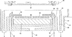
Fig. 1 is a kind of schematic diagram of flip-over type electroplanting device of traditional structure.As shown in Figure 1, tradition flip-over type electroplanting device comprises a cylindrical electroplating pool 312 that is open upwards, it is used to hold electroplate liquid 310, and a head 314, its be used for the surface of substrate W towards below state under substrate W of clamping semiconductor chip for example removably.The location of head 314 enables to cover the top open end of electroplating pool 312.In electroplating pool 312, Pingyang pole plate 316 horizontal arrangement and are immersed in the electroplate liquid 310.Positive plate 316 is as anode.The substrate W that by head 314 clampings has a neighboring, and this neighboring is connecting negative electrode by an electrode contacts that is located on the head 314.Positive plate 316 is made by porous material or Web materials.
The bottom center of electroplating pool 312 is connecting an electroplate liquid jet pipe 318, and this jet pipe is used to make the electroplate liquid in the electroplating pool 312 to form up-flow.The top of electroplating pool 312 by an electroplate liquid tank 302 round, this tank is used for holding the electroplate liquid that overflows from electroplating pool 312.Electroplate liquid jet pipe 318 is connecting an electroplate liquid supply pipe 328 that extends out from electroplate liquid regulating tank 322.Connecting a pump 324 and a filter 326 on the electroplate liquid supply pipe 328.Electroplate liquid regulating tank 322 is connecting an electroplate liquid return duct 330 that extends out from electroplate liquid fluid bowl 320.
This traditional electrical plating appts is following operation: the surface of substrate W towards below state under, substrate W by head 314 clampings, and is introduced downwards in the electroplating pool 312, thereby is immersed in the electroplate liquid 310 in the electroplating pool 312.Under certain voltage is applied to situation between positive plate 316 (anode) and the substrate W (negative electrode), electroplate liquid in the electroplate liquid regulating tank 322 upwards sprays from electroplating pool 312 bottoms through electroplate liquid jet pipe 318, and is applied to the form of jet flow on the lower surface (surface that will electroplate) of substrate W.In this way, along with electric current flows between positive plate 316 and substrate W, one deck plated film will be formed on the lower surface of substrate W.The electroplate liquid 310 that overflows from electroplating pool 312 this moment is reclaimed by electroplate liquid fluid bowl 320, and returns in the electroplate liquid regulating tank 322 through electroplate liquid return duct 330.
As previously mentioned, substrate is immersed in the electroplate liquid in electroplating the path.Connecting under the situation that dry state is arranged on the negative electrode on the head in substrate peripheral edge, wishing electrode contacts is connected on the substrate peripheral edge in the mode with respect to the electroplate liquid sealing fully.Therefore, electrode contacts need utilize a seal and seal with respect to electroplate liquid.Yet when implementing electroplating processes continuously, remaining electroplate liquid may adhere on seal and crystallization.The remaining electroplate liquid of crystallization on the seal causes the sealing property of seal to descend easily, thereby causes the conductance between substrate and the negative electrode impaired.In addition, after substrate was just electroplated, easy electroplate liquid because of remnants formed oxide-film on the surface of substrate.Therefore, after substrate was electroplated, substrate and seal needed to clean with clear water or analog immediately, thereby utilized clear water or analog to remove remaining electroplate liquid.
In conventional spray formula electroplanting device, the substrate that need be electroplated is kept by level and drops in the electroplating pool, so that continue to descend, so that in the whole lower surface immersion plating liquid of substrate again in the surface (spillwag chute) of the lower surface contact plating liquid of substrate.Therefore, after substrate is immersed in the electroplate liquid, comprise elements such as electrode contacts and seal in interior following outstanding part owing to exist, promptly therefore the substrate contact portion has bubble to be retained on the lower surface of substrate easily.Remaining bubble can hinder on the surface that electroplating film normally is formed on substrate, and produces such as defectives such as holes in plated film easily.
Summary of the invention
The present invention considers above-mentioned shortcoming and develops.Therefore, the purpose of this invention is to provide a kind of substrate processing device, its can clean efficiently substrate and with the contacted substrate contact portion of substrate, to remove electroplate liquid, and can increase the contacted tendentiousness of substrate and electroplate liquid, to realize high-quality processing.
In order to achieve the above object, according to an aspect of the present invention, provide a kind of substrate processing device that is used for treatment substrate, it comprises: head assembly, and it is used for the clamping substrate; And a plurality of substrate processing sections, their clamping to head assembly respectively substrates are handled accordingly; Wherein, head assembly can clamping substrate and is moved between the substrate processing section, and the respective handling that substrate is done is occurred in each substrate processing section successively.
Preferred construction is, substrate processing section comprises and be used for plating section that substrate is electroplated, and another substrate processing section comprises and is used for cleaning section that substrate is cleaned.Specifically, a kind of substrate processing device (electroplanting device) comprising: electroplate section, it has the electroplating pool that is used to hold electroplate liquid; Head assembly, it is used for the clamping substrate and substrate is immersed the electroplate liquid that is positioned at electroplating pool, so that form one deck plated film on the surface of substrate; Cleaning section, it is used to clean neighboring of electroplating substrate and the substrate contact portion that keeps in touch with substrate; And driving mechanism, it is used for head assembly is moved between plating section and cleaning section.
By this structure, owing to can under the state that substrate by the head assembly clamping, clean substrate lower surface and substrate contact portion, so can prevent residual effectively and attached to the electroplate liquid crystallization on the substrate contact portion.Like this, the durability of substrate contact portion can improve, and can realize high-quality electroplating process, can keep high conductivity again simultaneously.
Cleaning section can comprise hair-dryer, is used to supply for example nitrogen of clean air, so that the substrate drying.Perhaps, cleaning section can the high speed rotating substrate, so that the substrate drying.By this structure, can in a unit, implement clean and dried simultaneously.Therefore, substrate processing device can be of compact construction.In addition, the substrate contact portion can always keep dry.
Head assembly can comprise leaning device, is used for supporting substrate in tiltable mode.By this structure, the surface that will electroplate of substrate can contact with the overflow surface of electroplate liquid under the state that substrate is inclined relative to horizontal.Therefore, contacting tendentiousness and can improve between substrate and the electroplate liquid, thus make electroplate liquid can contact substrate reposefully, and can prevent that bubble from remaining on the surface that will electroplate of substrate.In addition, because substrate can keep vertical situation to have a down dip than wide-angle in the rotating shaft of head assembly, thereby the tilting action of substrate controls easily, and can have a down dip in less load.
Each processing section can be contained in the single outer cover.Be easy to generate smog around the electroplating pool, thereby can form highly corrosive environments around the electroplating pool.Outer cover can prevent effectively that smog from diffusing out.If driving mechanism is arranged in the outer cover outside, can prevents that then the particle that produces in the driving mechanism from entering in plating section and other sections, and prevent that the smog that produces in the electroplating process from acting on the driving mechanism nocuously, thereby can improve the durability of driving mechanism.In addition, if plating section and cleaning section are isolated from each other, then cleaning fluid can not mix with the electroplate liquid in the electroplating pool.Like this, the concentration of electroplate liquid can not change because of mixing cleaning fluid.Because electroplating section and cleaning section can combination with one another, so substrate processing device can be of compact construction generally.
Description of drawings
By the description of doing below in conjunction with accompanying drawing, above-mentioned and other purposes of the present invention, feature and advantage can clearly show, and the mode with example in the accompanying drawing shows the preferred embodiments of the present invention.
Fig. 1 is a kind of vertical cutaway view of traditional electrical plating appts;
Fig. 2 is the vertical view of substrate processing device according to an embodiment of the invention;
Fig. 3 is the vertical view of the electroplating unit in the substrate processing device shown in Figure 2;
Fig. 4 is the front view of electroplating unit shown in Figure 3;
Fig. 5 is the end view of electroplating unit shown in Figure 3;
Fig. 6 is the vertical cutaway view of the plating section in the electroplating unit shown in Figure 3;
Fig. 7 is the swing arm in the electroplating unit shown in Figure 3 and the vertical cutaway view of head assembly;
Fig. 8 is the vertical view of the substrate clamping limb assembly in the electroplating unit shown in Figure 3;
Fig. 9 is the cutaway view that the line IX-IX in Fig. 8 is done;
Figure 10 is the amplification view of the substrate contact portion among Fig. 9;
Figure 11 is the be connected to each other amplification view in zone of the rotating shaft of head assembly shown in Figure 7 and substrate clamping limb assembly;
Figure 12 is the front view of the cleaning section in the electroplating unit shown in Figure 3;
Figure 13 is the vertical view of the driving mechanism in the electroplating unit shown in Figure 3;
Figure 14 is the end view of driving mechanism shown in Figure 13;
Figure 15 is the cutaway view that the line XV-XV in Figure 13 is done;
Figure 16 is the cutaway view that the line XVI-XVI in Figure 13 is done;
Figure 17 is the vertical view of electroplating unit according to another embodiment of the invention;
Figure 18 is the schematic plan of an example of substrate electroplanting device;
Figure 19 is the air-flow schematic diagram in the substrate electroplanting device shown in Figure 180;
Figure 20 is the cutaway view of air-flow that is used for showing each district of substrate electroplanting device shown in Figure 180;
Figure 21 is the perspective view of substrate electroplanting device shown in Figure 180 when being placed in the clean room;
Figure 22 is the schematic plan of another example of substrate electroplanting device;
Figure 23 is the schematic plan of another example of substrate electroplanting device;
Figure 24 is the schematic plan of another example of substrate electroplanting device;
Figure 25 is the view of an organization plan example of semiconductor-based piece treating apparatus;
Figure 26 is the view of another organization plan example of semiconductor-based piece treating apparatus;
Figure 27 is the view of another organization plan example of semiconductor-based piece treating apparatus;
Figure 28 is the view of another organization plan example of semiconductor-based piece treating apparatus;
Figure 29 is the view of another organization plan example of semiconductor-based piece treating apparatus;
Figure 30 is the view of another organization plan example of semiconductor-based piece treating apparatus;
Figure 31 is the flow chart of each step in the semiconductor-based piece treating apparatus shown in Figure 30;
Figure 32 is the view of a schematic structure example of hypotenuse and dorsal part cleaning unit;
Figure 33 is the view of a schematic structure example of electroless plating apparatus;
Figure 34 is the view of another schematic structure example of electroless plating apparatus;
Figure 35 is the vertical cutaway view of an example of annealing unit;
Figure 36 is the transverse sectional view of annealing unit.
Embodiment
Below with reference to Fig. 2 to 16 substrate processing device in one embodiment of the present of invention is described.Fig. 2 is the vertical view of substrate processing device according to an embodiment of the invention.
Substrate processing device according to the embodiment of the invention is used as electroplanting device, and it is used for electro-coppering or suchlike metal on the surface of substrate.As shown in Figure 2, substrate processing device is positioned in the rectangular enclosure 1, so as to a plurality of substrates for example semiconductor chip electroplate continuously.Substrate processing device (electroplanting device) comprising: a pair of load/unload unit 10, they are respectively applied for and store a plurality of substrates, a pair of hypotenuse etching/chemical cleaning/drying unit 16, they are used to utilize chemical liquids to clean the plating substrate, pair of substrate stand 18, they are used for clamping substrate and upset substrate, and four electroplating units 22, and they are used for the plating substrate is electroplated and cleaned to substrate.Has first transmitting device 24 in the shell 1, be used between load/unload unit 10, hypotenuse etching/chemical cleaning/drying unit 16 and substrate stand 18, carrying substrate, and second transmitting device 28, be used between substrate stand 18 and electroplating unit 22, carrying substrate.
Substrate is contained in the substrate box with such state, and promptly the face side of each substrate (being used to form the surface that semiconductor device maybe will be handled) is towards the top.The substrate box that is holding substrate is placed on the load/unload unit 10.First transmitting device 24 takes out a substrate from the substrate box, substrate is transported to substrate stand 18 places, and substrate is placed on the substrate stand 18.On substrate stand 18, the turner that substrate is arranged in the substrate stand 18 spins upside down, and just is squeezed, so that its surface sides downwards.Afterwards, the substrate of being inverted is transported on second transmitting device 28 from substrate stand 18.Second transmitting device 28 is located the head assembly (will describe below) that substrate is transported to an electroplating unit 22, so that substrate is implemented electroplating processes.
Electroplating unit 22 in the electroplanting device of present embodiment is described below.Because the structure of all four electroplating units 22 is all identical, therefore only describe one of them below in detail.Fig. 3 is the vertical view of the electroplating unit 22 in the present embodiment, and Fig. 4 is the front view of electroplating unit 22 shown in Figure 3, and Fig. 5 is the end view of electroplating unit 22 shown in Figure 3.
Shown in Fig. 3 to 5, electroplating unit 22 is separated into two substrate processing sections by a partition 30, and promptly one is used for plating section 32 that substrate W is electroplated and one and is used to clean the cleaning section 34 of electroplating substrate W.Cleaning section 34 has to be held and carries substrate W, substrate W is carried out preliminary treatment and cleaning and dry function of electroplating substrate W.
Electroplating section 32 and cleaning section 34 by outer cover 36 cover caps.Outer cover 36 adjoins cleaning section 34 and has formed an opening 36a in its side plate, a gate 38 that is used for opening and closing opening 36a is arranged in opening 36a.Close opening 36a when sealing up the inside of electroplating unit 22 when gate 38, can prevent that the smog that results from the electroplating unit 22 is diffused into outside the electroplating unit 22 in the electroplating processes process.
Electroplating unit 22 has a swing arm 40 that is arranged in wherein, and it is used for doing oscillating motion around its pivot pin end between plating section 32 and cleaning section 34.Swing arm 40 has a free end, and this free end is connecting suspension head assembly 42 thereon, and a substrate W in the head assembly clamping.When swing arm 40 was done angular movement around its pivot pin end, head assembly 42 was being electroplated between plating position P in the section 32 and the cleaning positions Q in cleaning section 34 at one and is being done angular movement.
Property structure as an alternative, electroplating unit 22 also can have a straight-line motion mechanism but not swing arm 40, so that head assembly 42 is transmitted electroplating between plating position P in the section 32 and the cleaning positions Q in cleaning section 34.
Fig. 6 is the vertical cutaway view of major part of the plating section 32 in the electroplating unit 22.As shown in Figure 6, electroplate section 32 and have a cylindrical inboard spill piece 46 and a cylindrical outer side spill piece 48 that is used for holding the substantial cylindrical electroplating pool 44 of electroplate liquid and is arranged in electroplating pool 44.Inboard spill piece 46 has formed the bottom that 50, one anodes 52 of an electroplating chamber that is open upwards are arranged in electroplating chamber 50 in electroplating pool 44.
Be used for along the circumferential direction being located at the interval that equates the internal perisporium of inboard spill piece 46 to a plurality of electroplate liquid nozzles 54 of the central horizontal hydrojet of electroplating chamber 50.Electroplate liquid nozzle 54 is communicated with the electroplate liquid service duct 56 that vertically extends through inboard spill piece 46 inboards.Electroplate liquid is fed to the electroplate liquid nozzle 54 from an electroplate liquid regulating tank (not shown) through electroplate liquid service duct 56.Be used for being arranged between electroplate liquid service duct 56 and the electroplate liquid regulating tank with the control valve 58 of constant speed supply electroplate liquid.
First electroplate liquid row mouth 62 that is used for that the electroplate liquid in the electroplating chamber 50 is extracted out is formed on the bottom periphery part of electroplating chamber 50.Be used for footpath that second electroplate liquid row that the electroplate liquid of overflow by outside spill piece 48 discharged mouthfuls 64 is formed on outside spill piece 48 towards periphery.Be used for the 3rd electroplate liquid row mouth 66 that overflow is discharged by the electroplate liquid of inboard spill piece 46 is formed between inboard spill piece 46 and the outside spill piece 48.
Each first electroplate liquid row mouth 62 is connecting a container (not shown).A flow controller 68 is arranged between first electroplate liquid row mouth 62 and the described container.Each second electroplate liquid row mouth 64 all directly is being connected described container with each the 3rd electroplate liquid row mouth 66.Being transported to electroplate liquid in the described container is being driven from container by a pump and is being fed to the electroplate liquid regulating tank.A temperature controller (not shown) that is used for controlling the temperature of electroplating solution in the electroplate liquid regulating tank and one are housed in the electroplate liquid regulating tank are used for that electroplate liquid in the electroplate liquid regulating tank extracts and the plating solution analysis device (not shown) of analytical sample.
In the present embodiment, spoiler (liquid stream adjustable plate) 60 in electroplating chamber 50, be arranged in anode 52 above.Spoiler 60 will produce the electroplate liquid that flows to anode 52 and fall stream, and stream falls in this electroplate liquid will be by first electroplate liquid row mouthful 62 discharges.Spoiler 60 is used to prevent from directly to flow through from the electroplate liquid jet flow of electroplate liquid nozzle 54 ejections the surface of anode 52, is peeled off from anode 52 by the electroplate liquid jet flow to prevent the lip-deep black film that is formed on anode 52.
Fig. 7 is the vertical cutaway view of major part of swing arm 40 and head assembly 42.As shown in Figure 7, swing arm 40 is fixed on the upper end of a rotatable hollow leg 74, thereby can move horizontally along with the rotation of pillar 74.One by bearing 76 rotatably mounted rotating shaft 78 pass pillar 74, thereby can be with respect to pillar 74 rotations.A top swivel mount pulley 80 is fixed on the upper end of rotating shaft 78.
Rotating shaft 84 be can be rotated to support on the outer tube 82 by bearing 90, thereby can be with respect to outer tube 82 rotations.A head assembly pulley 92 is fixed on the upper end of rotating shaft 84.Head assembly pulley 92 is by a synchronous belt 94 top swivel mount pulley 80 that is being operably connected.Therefore, the rotating shaft 78 in pillar 74 is during around the rotation of self axis, and rotating shaft 84 will be with 86 rotations of substrate clamping limb assembly.
A bubble-tight seal cavity 98 is formed between moving member 96 and the outer tube 82 by a seal 97, and is communicated with an air feed passage 99.When air was optionally supplied in airtight sealing space 98 by air feed passage 99 or therefrom discharged, moving member 96 vertically moved with respect to outer tube 82.Moving member 96 has a plurality of depression bars 100 that are installed in the downward extension on its neighboring and a plurality ofly is used for the cylinder 104 that vertical mobile phase is answered thrust piece 102.
Fig. 8 is the vertical view of substrate clamping limb assembly 86, and Fig. 9 is the cutaway view that the line IX-IX in Fig. 8 is done.As shown in Figure 8, substrate clamping limb assembly 86 comprises that one is placed in the base 86a at center and six arm 86b that extend radially outwardly from base 86a.In these six arm 86b, three staggered arms of settling are supporting corresponding vertically carriage release lever 106 (see figure 9)s at their radial outer end respectively, and described vertical carriage release lever vertically extends through the neighboring of arm 86b.Nut 108 is installed in the upper end of vertical carriage release lever 106 respectively with such state, promptly helical compression spring 110 is clipped in respectively between nut 108 and the arm 86b.An annular substrate contact portion 112 of radially inwardly stretching out is fixed on the lower end of vertical carriage release lever 106.When the depression bar on the moving member 96 100 is resisted against on the nut 108 that is positioned at vertical carriage release lever 106 upper ends and is resisting the thrust of helical compression spring 110 and when driving vertical carriage release lever 106 and moving down, substrate contact portion 112 will move down from substrate clamping limb assembly 86, shown in the dotted line among Fig. 9.
Figure 10 is the amplification view of substrate contact portion 112.As shown in figure 10, a lip ring 114 is installed on the substrate contact portion 112.Lip ring 114 extends radially inwardly, and has an end that protrudes upward in its radial inner end.Substrate clamping limb assembly 86 have one with the terminal adjacent thrust piece that stretches out downwards 116 of protruding upward of lip ring 114.Helical compression spring 110 is selected as to have such spring performance, promptly when substrate contact portion 112 during with respect to mechanisms grip by being installed substrate W lifting, seal 114 will be pressed on the neighboring of substrate W, to seal up the compacted edge on the substrate W reliably.A cathode contact that links to each other with negative electrode 118 is arranged in seal 114 tops.When seal 114 will be pressed on the neighboring of substrate W, cathode contact 118 electrically contacted with substrate W.
Also have the corresponding mechanism 120 that is installed that is arranging with the angular spacing that equates on aforementioned three alternate arm 86b.As shown in Figure 9, each mechanism 120 that is installed comprises that respectively a base 122, on the upper surface that is installed in arm 86b is installed in bar 124 and the pawl 128 that can do angular movement around pivot 126 on the base 122 in the mode that can vertically move.Nut 130 is installed in the upper end of bar 124, and a helical compression spring 132 is clipped between nut 130 and the base 122.
As shown in Figure 9, pawl 128 is connecting bar 124 by a pin that can move horizontally 134.Like this, when bar 124 moves up, pawl 128 will radially inwardly be done angular movement around pivot 126, and when bar 124 moves down, pawl 128 will radially outward be done angular movement around pivot 126.After the cylinder on the moving member 96 104 is activated, thrust piece 102 will press against on the nut 130, and with downward catch bar 124, bar 124 will resisted the thrust of helical compression spring 132 and move down at this moment, so that pawl 128 is radially outward done angular movement around pivot 126.After the operation of cylinder 104 stops, bar 124 will upwards lift under the thrust of helical compression spring 132, so that pawl 128 is radially inwardly done angular movement around pivot 126.Therefore, the neighboring of the substrate W mechanism 120 that can be installed clamps.Specifically, the neighboring of substrate W is located and is grasped by three mechanisms 120 that are installed (pawl 128), thereby substrate W is clamped on the lower surface of substrate clamping limb assembly 86.
Figure 11 is the be connected to each other amplification view in zone of the rotating shaft 84 of head assembly 42 shown in Figure 7 and substrate clamping limb assembly 86.As shown in figure 11, dish type upper-part 140 is installed on the lower end of rotating shaft 84 of head assembly 42, and a dish type lower member 142 is installed on the upper surface of substrate clamping limb assembly 86.Upper-part 140 and lower member 142 are connected to each other by a horizontal pin 88, thereby constitute a leaning device, owing to can make lower member 142 and substrate clamping limb assembly 86 around pin 88 swings, but so leaning device supporting substrate clamping limb assembly 86 in the mode of squint.A helical compression spring 144 is clipped between the perimeter sides of upper-part 140 and lower member 142, be used under normal conditions described perimeter sides being pushed away each other, dogbolt 146 with the radially opposite position of helical compression spring 144 on be fixed on the perimeter sides of lower member 142.The upper end of dogbolt 146 can be resisted against on the lower surface of upper-part 140.When the upper end of dogbolt 146 was resisted against the lower surface of upper-part 140, substrate clamping limb assembly 86 by horizontal setting.A L shaped hook 148 is installed on the substrate clamping limb assembly 86.
Shown in Fig. 8 and 11, a cylinder 150 is installed on the outer tube 82 of head assembly 82, and a thrust piece 152 is connecting cylinder 150, vertically moves so that start the back at cylinder 150.After cylinder 150 starts, thrust piece 152 will descend and be resisted against on the upper end of hook 148, so that hook 148 is depressed.Like this, hook 148 and substrate clamping limb assembly 86 will resist helical compression spring 144 thrust and around pin 88 to lower swing.After the operation of cylinder 150 stops, hook 148 and substrate clamping limb assembly 86 will go back around pin 88 swings under the thrust of helical compression spring 144, dogbolt 146 is resisted against on the lower surface of upper-part 140, with 86 horizontal settings of substrate clamping limb assembly.
Next the cleaning section 34 of electroplating unit 22 is described.Figure 12 is the front view of cleaning section 34 shown in Figure 3.
Shown in Fig. 3 and 12, cleaning section 34 has six washer jets 160, is used to clean the substrate W that has been electroplated, and particularly electroplates the peripheral part of substrate W, and cleans substrate contact portion 112.Washer jet 160 is connecting a cleaning fluid source of supply (not shown), and cleaning fluid for example pure water sprays to the lower surface of substrate W from washer jet 160.Cleaning section 34 also has an arm shape hair-dryer 16, is used for the substrate W that has cleaned is carried out dried.Hair-dryer 162 is connecting an air source (not shown) by an air feed passage 164, and dry gas for example dry air or nitrogen sprays to the lower surface of substrate W from hair-dryer 162.Hair-dryer 162 can rotate around the one end, and this end is connecting the upper end of air feed passage 164.
As previously mentioned, pillar 74 can vertically move and can be around himself rotational, and the rotating shaft 78 that is arranged in the pillar 74 can be with respect to pillar 74 rotations.Next with reference to Figure 13 to 16 driving mechanism that is used for vertically mobile and rotation post 74 and rotating shaft 78 is described.Figure 13 is the vertical view of driving mechanism, and Figure 14 is the end view of driving mechanism, and Figure 15 is the cutaway view that the line XV-XV in Figure 13 is done, and Figure 16 is the cutaway view that the line XVI-XVI in Figure 13 is done.Shown in Figure 4 and 5, driving mechanism 170 is arranged in the outside of outer cover 36.Therefore, can prevent that the particle that driving mechanism 170 produces from entering in plating section 32 and other sections, and can prevent that the smog that produces in the electroplating process from acting on the driving mechanism 170 nocuously, to improve the durability of driving mechanism 170.
Shown in Figure 13 to 16, driving mechanism 170 mainly comprises a firm banking 172 and the vertical movable base 174 that can vertically be installed in movably on the firm banking 172 on the framework that is fixedly mounted on electroplating unit 22.Firm banking 172 upper supports a lifting motor 176, and vertically movable base 174 upper supports an electric rotating machine 178 and a swing motor 180.
As shown in figure 16, a screw shaft 182 that vertically extends is rotatably installed on the firm banking 172 by bearing 184.A nut 186 that is installed on the vertical movable base 174 keeps and screw shaft 182 engagements.A screw shaft pulley 188 is installed on the lower end of screw shaft 182, and by a synchronous belt 190 be operably connected one be installed in lifting motor 176 the axle on lifting motor pulley 192.Vertically movable base 174 has a slide block 196 (seeing Figure 15), and it is vertically led by a slide block bearing 194 that is loaded on the firm banking 172.After lifting motor 176 started, screw shaft 182 was around himself rotational, so that nut 186 and vertical movable base 174 vertically move, the slide block bearing 194 that while slide block 196 is loaded on the firm banking 172 is vertically guiding.
As shown in figure 15, a bottom swivel mount pulley 206 is installed on the lower end of the rotating shaft 78 of having passed pillar 74.Bottom swivel mount pulley 206 by a synchronous belt 208 be operably connected one be installed in electric rotating machine 178 the axle on electric rotating machine pulley 210.After electric rotating machine 178 started, rotating shaft 78 was rotated so that connecting the head assembly pulley 92 of top swivel mount pulley 80 around himself rotational, thereby drove rotating shaft 84 rotations of head assembly 42.
Electroplating process when utilization being described below for example semiconductor chip being electroplated to substrate according to the substrate processing device (electroplanting device) of present embodiment.
Substrate is contained in the substrate box with such state, and promptly the face side of each substrate (being used to form the surface that semiconductor device maybe will be handled) is towards the top.The substrate box that is holding substrate is placed on the load/unload unit 10.First transmitting device 24 takes out a substrate from the substrate box, substrate is transported to substrate stand 18 places, and substrate is placed on the substrate stand 18.On substrate stand 18, the turner that substrate is arranged in the substrate stand 18 spins upside down, and just is squeezed, so that its surface sides downwards.Afterwards, the substrate of being inverted is transported on second transmitting device 28 from substrate stand 18.The gate 38 of an electroplating unit 22 is opened, and second transmitting device 28 is transported to substrate in the electroplating unit 22 by the opening 36a on the outer cover 36.
For substrate being transported in the electroplating unit 22, the swing motor 180 of driving mechanism 170 is activated, so that pillar 74 is around the certain angle of himself rotational, thereby head assembly 42 is moved to cleaning positions Q.Afterwards, moving member 96 descends, so that depression bar 100 is resisted against on the nut 108 that is positioned at vertical carriage release lever 106 upper ends, and resisting the thrust of helical spring 110 and promotes vertical carriage release lever 106 downwards.Like this, substrate contact portion 112 can move down from substrate clamping limb assembly 86.
Next, the cylinder 104 on the moving member 96 starts, so that thrust piece 102 is resisted against on the nut 130 of the mechanism 120 that is installed.Subsequently, the thrust that bar 124 is being resisted helical spring 132 descends, so that pawl 128 is radially outward done angular movement.
The hand that stretches in the electroplating unit 22 on second transmitting device 28 lifts, and is resisted against on the thrust piece 116 of substrate clamping limb assembly 86 with the upper surface (dorsal part) with substrate W.In this state, the operation of cylinder 104 stops, and with release thrust piece 102, thereby the pawl 128 of the mechanism 120 that is installed is radially moved inward.Like this, substrate W is located and grasps by pawl 128.Afterwards, the hand of second transmitting device 28 is recalled from electroplating unit 22, and gate 38 is closed.
After the above-mentioned conveying release of substrate W, moving member 96 moves up, with lifting substrate contact portion 112.After substrate contact portion 112 was so lifted, the neighboring of substrate W promptly electrically contacted with cathode contact 118, and sealed 114 the sealing and can not be immersed in the electroplate liquid.After this, substrate W can be implemented preliminary treatment (precoating) by a kind of chemical liquids, and the washer jet 160 of this chemical liquids from cleaning section 34 sprays to the lower surface of substrate W.
Afterwards, the swing motor 180 of driving mechanism 170 starts, and so that pillar 74 is rotated a given angle, electroplates position P thereby the head assembly 42 that makes clamping substrate W moves to.The cylinder 150 of head assembly 42 starts, so that hook 148 interlocks of thrust piece 152 and substrate clamping limb assembly 86, and hook 148 is descended, thus substrate clamping limb assembly 86 is tilted by the angle in 1 ° to the 3 ° scope.After substrate clamping limb assembly 86 was so tilted, the lifting motor 176 of driving mechanism 170 started, and one section preset distance so that pillar 74 descends, the substrate W on the lower surface that is clamped in substrate clamping limb assembly 86 are immersed in the electroplate liquid in the electroplating pool 44.
When substrate W was so tilted and is immersed in the electroplate liquid, the surface of substrate W is the overflow surface of contact plating liquid gradually along with the decline of substrate W.Therefore, the surface of substrate W and the contact area of electroplate liquid are expanded gradually, thereby bubble is removed from the surface of substrate W.Therefore, contacting tendentiousness and can improve between substrate W and the electroplate liquid.Owing to have only substrate clamping limb assembly 86 to tilt, and the rotating shaft 84 of head assembly 42 meanwhile keeps vertically, so head assembly 42 and swing arm 40 do not need to tilt.Like this, substrate W can tilt than wide-angle, thereby the tilting action of substrate W controls easily, and can have a down dip in less load.Substrate clamping limb assembly 86 also can descend under its flat-hand position, and needn't tilt.
After in substrate W submerges electroplate liquid, the operation of cylinder 150 stops, so that substrate clamping limb assembly 86 returns its horizontal level.After this, the electric rotating machine 178 of driving mechanism 170 starts, rotate with the rotating shaft 84 that drives head assembly 42 by the rotating shaft in the pillar 74 78, thus the medium rotating speed rotation that substrate W is changeed with per minute about tens.Electric current is supplied between anode 52 and the substrate W, so that form plated film on the surface of substrate W.
After electroplating process finished, substrate W stopped the rotation.Cylinder 150 starts, so that in thrust piece 152 and hook 148 interlocks, and hook 148 is descended, thus substrate clamping limb assembly 86 is tilted by the angle in 1 ° to the 3 ° scope.Like this, can under action of gravity, easily fall attached to the remaining electroplate liquid on the lower surface of substrate W from substrate W.Under the situation that substrate clamping limb assembly 86 is so tilted, lifting motor 176 starts, one section preset distance so that pillar 74 and head assembly 42 raise.After this, the operation of cylinder 150 stops, so that substrate clamping limb assembly 86 returns its horizontal level.
Next, the swing motor of driving mechanism 170 180 starts, so that pillar 74 is around given angle of himself rotational, thereby the head assembly 42 that substrate W in clamping is moved to cleaning positions Q.Lifting motor 176 starts, one section preset distance so that pillar 74 descends.Afterwards, electric rotating machine 178 starts, so that substrate clamping limb assembly 86 rotary speeds with for example 100rpm revolve, meanwhile, cleaning fluid for example pure water sprays to the lower surface of substrate W from washer jet 160, electroplates substrate W and substrate contact portion 112 to clean.Owing to can under the state that substrate W by 86 clampings of substrate clamping limb assembly, clean the lower surface of electroplating substrate W and the substrate contact portion 112 of head assembly 42, therefore stay on the end of seal 114 of substrate contact portion 112 not having electroplate liquid after the substrate W release.Like this, according to the present invention, can prevent the sealing property and the conductance that cause because of remaining electroplate liquid crystallization and descend.
After this, the rotating speed of substrate clamping limb assembly 86 is brought up to for example 300rpm, so that the cleaning fluid rotation is got rid of.Meanwhile, air is fed on the substrate W from hair-dryer 162, so that substrate W drying.If only adopt the Rotary drying method, then substrate W will just can be dried with the speed rotation of 2000rpm usually.According to the present invention, owing to air is fed on the substrate W from hair-dryer 162, so substrate W need be with so high speed rotation.
Remove from substrate W and after substrate W is dried at cleaning fluid, moving member 96 descends, so that depression bar 100 is resisted against on the nut 108 that is positioned at vertical carriage release lever 106 upper ends and resisting the thrust of helical compression spring 110 and driving vertically that carriage release lever 106 moves down, thereby substrate contact portion 112 is moved down with respect to substrate W.
Next, the gate 38 of electroplating unit 22 is opened, and the hand of second transmitting device 28 stretches in the electroplating unit 22 by the opening 36a on the outer cover 36.Afterwards, the hand of second transmitting device 28 is lifted to the position that can receive substrate W.Subsequently, cylinder on the moving member 96 104 starts, so that thrust piece 102 is resisted against on the nut 130 of the mechanism 120 that is installed, and the thrust of resisting helical spring 132 reduces bar 124, so that pawl 128 is radially outward done angular movement.Substrate W is released and is placed on the hand of second transmitting device 28.After this, the hand band of second transmitting device 28 substrate W and is recalled from electroplating unit 22, and gate 38 is closed.
Though the present invention has been described with reference to preferred embodiment in the front, for the ordinary skill in the art, obviously under the premise without departing from the spirit and scope of the present invention, can make many modifications and variations.Next various feasible remodeling embodiment are described.
A flow container that is used for substrate W is immersed in electroplate liquid can be installed in the cleaning section 34.In this case, substrate W can stand preliminary treatment in electroplating unit 22, for example preimpregnation or preplating.Prepreg process is such process, promptly in an on-chip successive sedimentation apply a kind of homogeneous film that contains the preliminary treatment liquid (presoak) of electroplating bath components on the surface of separator and crystal grain layer, to improve electroplate liquid to on-chip adhesive performance.The preplating process is such process, promptly in an on-chip successive sedimentation implement preplating on the surface of separator and crystal grain layer, to strengthen uncompleted crystal grain layer.
Figure 17 is the vertical view of electroplating unit according to another embodiment of the invention.As shown in figure 17, electroplating unit has a plurality of substrate processing sections, and comprising a preplating section 250, a preliminary treatment/reprocessing/cleaning section 251 and a second time electroplating section 252, they are arranged round pillar 74, are fixing swing arm 40 on the pillar.Like this, utilize a plurality of substrate processing sections, can in single electroplating unit 22, implement different processing.
As previously mentioned, according to the present invention, owing to can under the state that substrate by the head assembly clamping, clean substrate lower surface and substrate contact portion, so can prevent residual effectively and attached to the electroplate liquid crystallization on the substrate contact portion.Like this, the durability of substrate contact portion can improve, and can realize high-quality electroplating process, can keep high conductivity again simultaneously.
In addition, be isolated from each other owing to electroplating section and cleaning section, so cleaning fluid can not mix with the electroplate liquid in the electroplating pool.Like this, the concentration of electroplate liquid can not change because of mixing cleaning fluid.
Because the substrate processing section is covered with by an outer cover, therefore can prevent that the smog that produces in the outer cover is diffused into outside the outer cover.In addition, because driving mechanism is arranged in the outer cover outside, can prevent that therefore the particle that produces in the driving mechanism from entering in plating section and other sections.Can also prevent that the smog that produces in the electroplating process from acting on the driving mechanism nocuously, thereby can improve the durability of driving mechanism.Because different element can combination with one another, so substrate processing device can be of compact construction generally.
In addition, according to the present invention, the surface that will electroplate of substrate can contact with the overflow surface of electroplate liquid under the state that substrate is inclined relative to horizontal.Therefore, contacting tendentiousness and can improve between substrate and the electroplate liquid, thus make electroplate liquid can contact substrate reposefully, and can prevent that bubble from remaining on the surface that will electroplate of substrate.In addition, because substrate can keep vertical situation to have a down dip than wide-angle in the rotating shaft of head assembly, thereby the tilting action of substrate controls easily, and can have a down dip in less load.
Figure 18 is the schematic plan of an example of substrate electroplanting device.Substrate electroplanting device shown in Figure 18 comprises: a load/unload district 520, it is holding the substrate box that semiconductor chip is housed, a treatment region 530, and it is used for semiconductor chip is handled, and a cleaning-drying district 540, it is used for cleaning and dry electroplating of semiconductor substrate.Cleaning-drying district 540 is placed between load/unload district 520 and the treatment region 530.A partition 521 is arranged between load/unload district 520 and the cleaning-drying district 540.A partition 523 is arranged between cleaning-drying district 540 and the treatment region 530.
Formed a passage (not shown) in the partition 521, this passage is used for semiconductor chip is carried between load/unload district 520 and cleaning-drying district 540, and is supporting a gate 522 that is used to open and close this passage.Also formed a passage (not shown) in the partition 523, this passage is used for semiconductor chip is carried between cleaning-drying district 540 and treatment region 530, and is supporting a gate 524 that is used to open and close this passage.Cleaning-drying district 540 and treatment region 530 can be supplied separately and discharged air.
Substrate electroplanting device shown in Figure 18 is positioned in the clean room that is holding semiconductor manufacturing facility.Pressure in load/unload district 520, treatment region 530 and the cleaning-drying district 540 is following selection:
Pressure in pressure>treatment region 530 in pressure in the load/unload district 520>cleaning-drying district 540.
Pressure in the load/unload district 520 is lower than the pressure in the clean room.Like this, air can not flow into the cleaning-drying district 540 from treatment region 530, and air can be from 540 inflow load/unload districts 520, cleaning-drying district yet.In addition, air can be from load/unload district 520 inflow clean rooms.
Arrange a loading unit 520a and a unloading unit 520b in the load/unload district 520, holding a substrate box that is used to deposit semiconductor chip in these two unit respectively.Holding two in the cleaning-drying district 540 is used to utilize water to clean water cleaning unit 541 and two drying units 542 that are used for dry electroplating of semiconductor substrate of electroplating of semiconductor substrate.Each water cleaning unit 541 can comprise a penholder shape washer or the roller that spongy layer is housed that spongy layer is housed at front end on outer surface.Each drying unit 542 can comprise a drier, is used for the high speed rotating semiconductor chip, to realize dehydration and dry.Also has a transmission unit (transferring robot) 543 that is used to carry semiconductor chip in the cleaning-drying district 540.
Holding in the treatment region 530 and be used for before electroplating a plurality of pretreatment chamber 531 of semiconductor chip preheating and be used for the copper-plated a plurality of electroplating chambers 532 of semiconductor chip.Also has a transmission unit (transferring robot) 543 that is used to carry semiconductor chip in the treatment region 530.
Figure 19 there is shown air-flow in the substrate electroplanting device in side-looking.As shown in figure 19, fresh air is introduced from the external world by a conduit 546, and forced to drive from top board 540a by fan and flow into the cleaning-drying districts 540, thereby form the fresh air that flows downward round water cleaning unit 541 and drying unit 542 through high-performance filter 544.The fresh air of most of supply returns top board 540a by circulation conduit 545 from base plate 540b, and from here on, fresh air is forced driving by fan again and passed through filter 544 and flow into once more in the cleaning-drying district 540.Part fresh air flows out cleaning-drying district 540 from water cleaning unit 541 and drying unit 542 by conduit 522.
In the treatment region 530 that is holding pretreatment chamber 531 and electroplating chamber 532,, do not allow on the surface that particle is applied to semiconductor chip even treatment region 530 is positioned at wet district yet.In order to prevent that particle is applied on the semiconductor chip, downward fresh air flows round pretreatment chamber 531 and electroplating chamber 532.Fresh air is introduced from the external world through conduit 539, and is forced driving from top board 530a through the high-performance filter 533 inflow treatment regions 530 by fan.
If the fresh air of introducing in the treatment region 530 that constitutes downward fresh air stream is generally always supplied into from the external world, then a large amount of air need be introduced in the treatment region 530 always and discharge.According to this embodiment, air is discharged from treatment region 530 with the rate of discharge that is enough to keep pressure in the treatment region 530 to be lower than pressure in the cleaning-drying district 540 through conduit 533, and introduces the fresh air that the major part in the treatment region 530 flows downward and will cycle through circulation conduit 534,535.Circulation conduit 534 begins from cleaning-drying district 540 to extend, and is connecting the filter 533 that is positioned at top board 530a top.Circulation conduit 535 is arranged in the cleaning-drying district 540, and is connecting conduit 534 parts that are arranged in cleaning-drying district 540.
Flow through and contain from chemical fog in the solution pool and gas in the circulating air of treatment region 530.By being arranged in washer 536 and the smoke separator 537,538 in conduit 534 parts that link to each other with conduit 535, chemical fog and gas are got rid of from circulating air.Like this, air begins to cycle through washer 536 and smoke separator 537,538 from cleaning-drying district 540, returns the circulation conduit 534 that is arranged in top board 530a top again, thereby has eliminated all chemical fogs and gas.This cleaned air is forced to drive the filter 533 and returning in the treatment region 530 of flowing through by fan again.
Portion of air is passed through the conduit 535 that links to each other with the base plate 530b of treatment region 530 and is discharged from treatment region 530.The air that contains chemical fog and gas is also discharged from treatment region 530 through conduit 553.Be fed to the electroplating chamber 530 from conduit 539 under the effect that for dead room pressure, results from the negative pressure in the electroplating chamber 530 with the fresh air of the air equivalent of discharging through conduit 553.
As previously mentioned, the pressure in the load/unload district 520 is higher than the pressure in the cleaning-drying district 540, and the latter is higher than the pressure in the treatment region 530 again.After gate 522,524 (seeing Figure 18) is opened, air will flow through load/unload district 520, cleaning-drying district 540 and treatment region 530 successively, as shown in figure 20.Extend to the common conduit 554 (seeing Figure 21) of clean room outside through conduit 552,553 one of inflow from the air of cleaning-drying district 540 and treatment region 530 discharges.
Perspective view when substrate electroplanting device shown in Figure 180 being shown among Figure 21 being placed in the clean room.Load/unload district 520 comprises a sidewall, and this sidewall has the boxlike delivery port 555 and the control board 556 that are formed on wherein, and is exposed in the operation interval 558 that is isolated from clean room by partition 557.Partition 557 also isolates between the battery limits that the substrate electroplanting device is installed 559 from clean room.Other sidewalls of substrate electroplanting device are exposed between the battery limits that air cleanliness is lower than operation interval 558 in 559.
As previously mentioned, cleaning-drying district 540 is arranged between load/unload district 520 and the treatment region 530.Partition 521 is arranged between load/unload district 520 and the cleaning-drying district 540.Partition 523 is arranged between cleaning-drying district 540 and the treatment region 530.A drying of semiconductor substrate is loaded into the substrate electroplanting device by boxlike delivery port 555 from operation interval 558, electroplates in the substrate electroplanting device again.The semiconductor chip of having electroplated is cleaned and is dry, is unloaded to the operation interval 558 from the substrate electroplanting device by boxlike delivery port 555 again.Therefore, do not have on the surface that particle and smog is applied to semiconductor chip, and can prevent that air cleanliness is higher than between battery limits 559 operation interval 558 and is infected with by particle, chemical fog and cleaning fluid mist.
In the embodiment shown in Figure 18 and 19, the substrate electroplanting device has load/unload district 520, cleaning-drying district 540 and treatment region 530.Yet, also a district that is holding the chemical-mechanical polishing unit can be arranged in the treatment region 530 or near, and cleaning-drying district 540 can be arranged in the treatment region 530 or between district that is holding the chemical-mechanical polishing unit and load/unload district 520.Other any suitable districts and arrangements of cells mode all can adopt, as long as the drying of semiconductor substrate can be loaded in the substrate electroplanting device, the electroplating of semiconductor substrate can be cleaned and drying also unloads from the substrate electroplanting device subsequently.
Among this embodiment of Miao Shuing, the present invention is applied in the substrate electroplanting device that is used for the electroplating of semiconductor substrate in the above.Yet principle of the present invention also can be applied in the substrate electroplanting device of the substrate that is used for electroplating except that semiconductor chip.In addition, the zone that utilizes the substrate electroplanting device to electroplate on substrate is not limited to on-chip wiring zone.The substrate electroplanting device also can be used to electroplate the metal outside the copper removal.
Figure 22 is the vertical view of another example of substrate electroplanting device.Substrate electroplanting device shown in Figure 22 comprises a loading unit 601 that is used to load semiconductor chip, one is used for copper-plated copper facing chamber 602 on semiconductor chip, be used for a pair of water purge chamber 603 and 604 that water cleans semiconductor chip, a cmp unit 605 that is used for chemistry and mechanical polishing semiconductor chip, be used for a pair of water purge chamber 606 and 607 that water cleans semiconductor chip, hothouse 608 that is used for the drying of semiconductor substrate and one be used for having the plated film that connects up the semiconductor chip unloading carry carrier unit 609.The substrate electroplanting device also has a substrate transmission mechanism (not shown), is used for semiconductor chip is carried in described chamber 602,603,604, and cmp unit 605, described chamber 606,607,608, and between the unloading unit 609.Loading unit 601, chamber 602,603,604, cmp unit 605, chamber 606,607,608, and unloading unit 609 has been formed the single formula overall structure of device.
The substrate electroplanting device is following operation: substrate transmission mechanism is transported to a semiconductor chip W who does not form the wiring plated film as yet in the copper facing chamber 602 from a substrate box 601-1 who is placed on the loading unit 601.In copper facing chamber 602, the layer of copper plated film is formed on the surface of semiconductor chip W, has the wiring zone of being made up of wire laying slot and routing hole (contact hole) on this surface.
After plated copper film was formed on the semiconductor chip W in copper facing chamber 602, semiconductor chip W was transported in the water purge chamber 603,604 by substrate transmission mechanism, and was cleaned by water in a described water purge chamber 603,604.Semiconductor chip W after the cleaning is transmitted mechanism and is transported in the cmp unit 605.Cmp unit 605 is removed useless plated copper film from the surface of semiconductor chip W, stay the plated copper film part in wire laying slot and the routing hole.A separator that is made of TiN or similar material was formed on the surface of semiconductor chip W before the copper coating deposition, comprised the inner surface of wire laying slot and routing hole.
Next, the semiconductor chip W that has the residual copper plated film is transported in the water purge chamber 606,607 by substrate transmission mechanism, and is cleaned by water in a described water purge chamber 606,607.Semiconductor chip W after the cleaning is dried in hothouse 608, and afterwards, the semiconductor chip W that has the residual copper plated film that is used as the wiring film is placed into the substrate box 609-1 that is arranged in unloading unit 609.
Figure 23 is the vertical view of another example of substrate electroplanting device.The difference of substrate electroplanting device is shown in the electroplanting device of substrate shown in Figure 23 and Figure 22, an additional copper facing chamber 602, water purge chamber 610, pretreatment chamber 611, protective layer electroplating chamber 612, water purge chamber 613 and 614 and cmp unit 615 that are used for forming protective layer on the copper coating of semiconductor chip of having comprised.Loading unit 601, chamber 602,602,603,604,614, cmp unit 605,615, chamber 606,607,608,610,611,612,613, and unloading unit 609 has been formed the single formula overall structure of device.
The electroplanting device of substrate shown in Figure 23 is following operation: semiconductor chip W is transported in the copper facing chamber 602,602 successively from a substrate box 601-1 who is placed on the loading unit 601.In a described copper facing chamber 602,602, the layer of copper plated film is formed on the surface of semiconductor chip W, has the wiring zone of being made up of wire laying slot and routing hole (contact hole) on this surface.Adopt two copper facing chambers 602,602, make that semiconductor chip W can be with the time electroplating copper film of lengthening, specifically, semiconductor chip W can electroplate the elementary copper film of last layer in the mode of electroless plating in a copper facing chamber 602, and then electroplates last layer secondary copper film in the mode of metallide in another copper facing chamber 602.The substrate electroplanting device can have plural copper facing chamber.
Having formed the semiconductor chip W behind the plated copper film is cleaned by water in a water purge chamber 603,604.Afterwards, cmp unit 605 is removed useless plated copper film from the surface of semiconductor chip W, stays the plated copper film part in wire laying slot and the routing hole.
Next, the semiconductor chip W that has the residual copper plated film is transported in the water purge chamber 610, and at this, semiconductor chip W is cleaned by water.Afterwards, semiconductor chip W is transported in the pretreatment chamber 611 also pretreated, with deposition one deck protective coating.Pretreated semiconductor chip W is transported in the protective layer electroplating chamber 612.In protective layer electroplating chamber 612, protective coating is formed on above the plated copper film in the wiring zone of semiconductor chip W.As example, protective coating can constitute by the alloy of electroless plating by nickel (Ni) and boron (B).
After semiconductor chip was cleaned in a water purge chamber 613 and 614, in cmp unit 615, the top that is deposited on the protective coating on the copper coating was ground away, so that the protective coating complanation.
After protective coating was ground, semiconductor chip W was cleaned by water in a water purge chamber 606,607.Semiconductor chip W after the cleaning is transmitted mechanism and is transported in the hothouse 608, is dried in hothouse 608, is transported to the substrate box 609-1 that is arranged in unloading unit 609 again.
Figure 24 is the vertical view of another example of substrate electroplanting device.As shown in figure 24; the substrate electroplanting device comprises a robot 616 that is positioned at its center and has mechanical arm 616-1; the substrate electroplanting device also has a copper facing chamber 602, a pair of water purge chamber 603 and 604, cmp unit 605, pretreatment chamber 611, protective layer electroplating chamber 612, a hothouse 608 and a load/unload station 617; they are arranged round robot 616, and are positioned at the coverage of mechanical arm 616-1.The unloading unit 609 that loading unit 601 that is used to load semiconductor chip and one are used to unload semiconductor chip adjoins load/unload station 617 and arranges.Robot 616, chamber 602,603,604, cmp unit 605, chamber 608,611,612, load/unload station 617, loading unit 601, and unloading unit 609 has been formed the single formula overall structure of device.
The electroplanting device of substrate shown in Figure 24 is following operation:
The semiconductor chip that will be electroplated is transported to the load/unload station 617 from loading unit 601, and at this, semiconductor chip is received by mechanical arm 616-1, and is transported in the copper facing chamber 602.In copper facing chamber 602, the layer of copper plated film is formed on the surface of semiconductor chip, has the wiring zone of being made up of wire laying slot and routing hole on this surface.The semiconductor chip that has plated copper film is transported in the cmp unit 605 by mechanical arm 616-1.In cmp unit 605, useless plated copper film is removed from the surface of semiconductor chip W, stays the plated copper film part in wire laying slot and the routing hole.
Afterwards, semiconductor chip is transported in the water purge chamber 604 by mechanical arm 616-1, and at this, semiconductor chip is cleaned by water.After this, semiconductor chip is transported in the pretreatment chamber 611 by mechanical arm 616-1, and at this, semiconductor chip is pretreated, with deposition one deck protective coating.Pretreated semiconductor chip is transported in the protective layer electroplating chamber 612 by mechanical arm 616-1.In protective layer electroplating chamber 612, protective coating is formed on above the plated copper film in the wiring zone of semiconductor chip W.The semiconductor chip that has formed protective coating is transported in the water purge chamber 604 by mechanical arm 616-1, and at this, semiconductor chip is cleaned by water.After this, semiconductor chip is transported in the hothouse 608 by mechanical arm 616-1, and at this, semiconductor chip is dried.Dried semiconductor chip is transported in the load/unload station 617 by mechanical arm 616-1, and the electroplating of semiconductor substrate is transported in the unloading unit 609 more from here.
Figure 25 is the view of another organization plan example of semiconductor-based piece treating apparatus.Semiconductor chip is such structure, promptly is provided with a load/unload station 701, plated copper film and forms unit 702, first robot 703, the 3rd cleaning machine 704, tipper 705, tipper 706, second cleaning machine 707, second robot 708, first cleaning machine 709, first lapping device 710 and second lapping device 711.One be used for before electroplating and measure the plating of coating film thickness afterwards before and plating back film thickness measuring instrument 712 and one be used for after grinding dry state and measure the dry state film thickness measuring instrument 713 of the thickness of semiconductor chip W and adjoin first robot 703 and place.
First lapping device (grinding unit) 710 have a grinding table 710-1 ,-ring 710-2 is inhaled at individual top, ring a 710-3, a film thickness measuring instrument 710-4 and a thrust piece 710-5 are inhaled in a top.Second lapping device (grinding unit) 711 has a grinding table 711-1, ring 711-2, top suction ring a 711-3, a film thickness measuring instrument 711-4 and a thrust piece 711-5 are inhaled in a top.
A substrate box 701-1 who is holding semiconductor chip W is placed on the load ports at load/unload station 701, has formed the through hole and the groove that are used to connect up among the semiconductor chip W, and has formed a crystal grain layer on the semiconductor chip W.First robot 703 takes out semiconductor chip W from substrate box 701-1, and semiconductor chip W is transported in the plated copper film formation unit 702 that is used to form plated copper film.At this moment, before crystal grain layer thickness is plated and plating back film thickness measuring instrument 712 is measured.Plated copper film is so to form, and promptly earlier hydrophilic treated is implemented on the surface of semiconductor chip W, and then copper facing.After having formed plated copper film, will form in the unit 702 semiconductor chip W washing or cleaning at plated copper film.
Semiconductor chip W formed from plated copper film by first robot 703 take out the unit 702 after, before the thickness of copper coating is plated and plating back film thickness measuring instrument 712 is measured.The result who measures is recorded in the tape deck (not shown) as the record data of semiconductor chip, and is used to judge that plated copper film forms unit 702 and whether occurs unusually.After having measured thickness, first robot 703 is transported to semiconductor chip W in the tipper 705, and tipper 705 is with semiconductor chip W upset (make and formed the downwards surperficial of copper coating).First lapping device 710 and second lapping device 711 are implemented to grind with series model and paralleling model.The grinding operation of series model is described below.
In the grinding operation of series model, utilize first lapping device 710 to implement first the grinding, utilize second lapping device 711 to implement regrind again.Second robot 708 picks up the semiconductor chip W that is positioned on the tipper 705, and semiconductor chip W is placed on the thrust piece 710-5 of lapping device 710.The top is inhaled ring 710-2 and is utilized suction adsorption firmly to be positioned at semiconductor chip W on the thrust piece 710-5, and makes the plated copper film surface of semiconductor chip W contact the abradant surface of grinding table 710-1 under pressure, to implement first grinding.By first grinding, plated copper film is ground away basically.The abradant surface of grinding table 710-1 by polyurathamc for example IC1000 constitute, perhaps constitute by material fixing or that embedded abrasive grains.Along with the relative motion between abradant surface and the semiconductor chip W, plated copper film is ground away.
Behind the grinding operation of having finished plated copper film, semiconductor chip W is being driven by top suction ring 710-2 and is returning on the thrust piece 710-5.Second robot 708 picks up semiconductor chip W, and is introduced in first cleaning machine 709.At this moment, a kind of chemical liquids can be ejected on the surface and dorsal part of the semiconductor chip W that is positioned on the thrust piece 710-5, to remove particle or to cause particle to be difficult to attached on the semiconductor chip W.
Behind the cleaning operation in having finished first cleaning machine 709, second robot 708 picks up semiconductor chip W, and places it on the thrust piece 711-5 of second lapping device 711.The top is inhaled ring 711-2 and is utilized suction adsorption to be positioned at semiconductor chip W on the thrust piece 711-5, and makes the surface that is formed with separator on the semiconductor chip W contact abradant surface of grinding table 711-1 under pressure, with the enforcement regrind.The structure of grinding table 711-1 is identical with grinding table 710-1 basically.By regrind, separator is ground away basically.Yet, after first the grinding, having stayed under the situation of plated copper film and oxide-film, these films also can be ground away.
The abradant surface of grinding table 711-1 by polyurathamc for example IC1100 constitute, perhaps constitute by material fixing or that embedded abrasive grains.Along with the relative motion between abradant surface and the semiconductor chip W, grinding operation is implemented.In this case, quartz, corundum, ceria or similar material can be used as abrasive grains or slurry.The type of the plated film that a kind of chemical liquids is ground is as required allocated out.
The detection of the terminating point of regrind is achieved in that the thickness that promptly mainly utilizes the blooming measuring instrument to measure separator, and surveys the thickness vanishing or comprise the time that expose on the insulation film surface of SiO2.In addition, the film thickness measuring instrument that has an image processing function is used as near the film thickness measuring instrument 711-4 that is located at the grinding table 711-1.By using this measuring instrument, can measure the thickness of oxide-film, measurement result is stored the processing procedure record into semiconductor chip W, and is used for judging whether implemented the semiconductor chip W after the regrind can be transported to next step.If do not reach the terminating point of regrind, then need to implement to grind again.If because of certain abnormal conditions cause overmastication, then semiconductor-based piece treating apparatus is shut down, to avoid producing more waste product in ensuing grinding operation.
After having finished regrind, semiconductor chip W is inhaled ring 711-2 by the top and moves on the thrust piece 711-5.Second robot 708 picks up the semiconductor chip W that is positioned on the thrust piece 711-5.At this moment, a kind of chemical liquids can be ejected on the surface and dorsal part of the semiconductor chip W that is positioned on the thrust piece 711-5, to remove particle or to cause particle to be difficult to attached on the semiconductor chip W.
After having finished above-mentioned cleaning, second robot 708 picks up semiconductor chip W, and is transported in the tipper 706, and tipper 706 overturns semiconductor chip W.The semiconductor chip W that has overturn is picked up by first robot 703, and is transported in the 3rd cleaning machine 704.In the 3rd cleaning machine 704, respond to the surface that water is sprayed to semiconductor chip W by the magnetosonic that ultrasonic vibration activates, to clean semiconductor chip W.At this moment, the surface of semiconductor chip W can utilize a kind of cleaning fluid to clean by known penholder shape sponge washer, and cleaning fluid is made by pure water, and has added surfactant, chelating agent or pH value conditioning agent.Afterwards, semiconductor chip W dries by rotation and is dried.
As previously mentioned, near film thickness measuring instrument 711-4 measured if thickness has been arranged on grinding table 711-1, and then semiconductor chip W need not stand additional treatments, and can be loaded into the substrate box that is arranged on the 701 unloading mouths of load/unload station.
Figure 26 is the view of another organization plan example of semiconductor-based piece treating apparatus.The difference of this substrate processing device and substrate processing device shown in Figure 25 is, is provided with an over-plated unit 750, forms unit 702 with the plated copper film that replaces among Figure 25.
The substrate box 701-1 of a semiconductor chip W who is holding to be formed with plated copper film is placed on the load ports at load/unload station 701.The semiconductor chip W that takes out from substrate box 701-1 is transported in first lapping device 710 or second lapping device 711, so that the plated copper film surface grinding is fallen.After the grinding of having finished the plated copper film surface, semiconductor chip W cleans in first cleaning machine 709.
Behind the cleaning operation in having finished first cleaning machine 709, semiconductor chip W is transported in the over-plated unit 750, at this, over-plated is implemented on plated copper film surface, and is oxidized to prevent plated copper film to be subjected to the effect of atmosphere.The semiconductor chip of having implemented after over-plated is operated is transported to second cleaning machine 707 from over-plated unit 750 by second robot 708, is cleaned by pure water or deionized water at this.After having finished cleaning, semiconductor chip turns back among the substrate box 701-1 that is put on the load/unload station 701.
Figure 27 is the view of another organization plan example of semiconductor-based piece treating apparatus.The difference of this substrate processing device and substrate processing device shown in Figure 26 is, is provided with an annealing unit 751, to replace the 3rd cleaning machine 709 among Figure 26.
Semiconductor chip W after grinding in grinding unit 710 or 711 as previously mentioned and cleaning in first cleaning machine 709 is transported in the over-plated unit 750, at this, over-plated is implemented on the plated copper film surface.The semiconductor chip of having implemented after over-plated is operated is transported to first cleaning machine 709 from over-plated unit 750 by second robot 708, and is cleaned at this.
Behind the cleaning operation in having finished first cleaning machine 709, semiconductor chip W is transported in the annealing unit 751, stands annealing in process at this substrate, so that the plated copper film alloying, thereby the electromigration resistance of increase plated copper film.Stood the semiconductor chip W after the annealing in process and be transported to second cleaning machine 707, cleaned by pure water or deionized water at this from annealing unit 751.After having finished cleaning, semiconductor chip turns back among the substrate box 701-1 that is put on the load/unload station 701.
Figure 28 is the view of another organization plan example of semiconductor-based piece treating apparatus.In as 28, represent identical or corresponding part with Reference numeral identical among Figure 25.In this routine substrate processing device, a pushing protractor 725 adjoins first lapping device 710 and second lapping device, 711 layouts.Substrate mounting table 721,722 adjoins the 3rd cleaning machine 704 respectively and plated copper film forms unit 702 layouts.A robot 723 adjoins first cleaning machine 709 and the 3rd cleaning machine 704 layouts.In addition, a robot 724 adjoins second cleaning machine 707 and plated copper film formation unit 702 layouts, and a dry state film thickness measuring instrument 713 adjoins load/unload station 701 and 703 placements of first robot.
In having the substrate processing device of said structure, first robot 703 will take out the substrate box 701-1 of semiconductor chip W on the load ports that is placed on load/unload station 701.After utilizing dry state film thickness measuring instrument 713 to measure the thickness of separator and crystal grain layer, first robot 703 is placed on semiconductor chip W on the substrate mounting table 721.Under the situation when dry state film thickness measuring instrument 713 is located at first robot, 703 hands, thickness is measured on this hand, and meron is placed on the substrate mounting table 721.The semiconductor chip W that second robot 723 will be arranged on the substrate mounting table 721 is transported to plated copper film formation unit 702, forms plated copper film at this.After having formed plated copper film, before the thickness of copper coating is plated and plating back film thickness measuring instrument 712 is measured.Afterwards, second robot 723 is transported to pushing protractor 725 with semiconductor chip W and loads thereon.
[series model]
In series model, the top is inhaled ring 710-2 and is utilized suction adsorption firmly to be positioned at semiconductor chip W on the pushing protractor 725, is transported to grinding table 710-1, and with semiconductor chip W by on the abradant surface that is pressed in grinding table 710-1, to implement grinding operation.The detection of the terminating point that grinds is to utilize with identical method noted earlier to realize.Finishing semiconductor chip W after the grinding is inhaled ring 710-2 by the top and is transported to pushing calibration 725 and loads thereon.Second robot 723 takes off semiconductor chip W, and is transported in first cleaning machine 709, to implement cleaning.Afterwards, semiconductor chip W is transported to pushing protractor 725 and loads thereon.
The top is inhaled ring 711-2 and is utilized suction adsorption firmly to be positioned at semiconductor chip W on the pushing protractor 725, is transported to grinding table 711-1, and with semiconductor chip W by on the abradant surface that is pressed in grinding table 711-1, to implement grinding operation.The detection of the terminating point that grinds is to utilize with identical method noted earlier to realize.Finishing semiconductor chip W after the grinding is inhaled ring 711-2 by the top and is transported to pushing protractor 725 and loads thereon.The 3rd robot 724 picks up semiconductor chip W, and its thickness is measured by a film thickness measuring instrument 726.Afterwards, semiconductor chip W is transported in second cleaning machine 707, to implement cleaning.Then, semiconductor chip W is transported in the 3rd cleaning machine 704, is dried thereby be cleaned and dry by rotation.Afterwards, semiconductor chip W is picked up by the 3rd robot 724, and is placed on the substrate mounting table 722.
[paralleling model]
In paralleling model, ring 710-2 is inhaled at the top or 711-2 utilizes suction adsorption firmly to be positioned at the semiconductor chip W that pushes on the protractor 725, be transported to grinding table 710-1 or 711-1, and with semiconductor chip W by on the abradant surface that is pressed in grinding table 710-1 or 711-1, to implement grinding operation.After having measured thickness, the 3rd robot 724 picks up semiconductor chip W, and is placed on the substrate mounting table 722.
The semiconductor chip W that first robot 703 will be positioned on the substrate mounting table 722 is transported on the dry state film thickness measuring instrument 713.After having measured thickness, semiconductor chip turns back among the substrate box 701-1 that is put on the load/unload station 701.
Figure 29 is the view of another organization plan example of semiconductor-based piece treating apparatus.This substrate processing device is such substrate processing device, promptly can not form a crystal grain layer of formation and a plated copper film on the semiconductor chip W of crystal grain layer as yet, and is grinding these films, to form wiring.
In this substrate processing device, a pushing protractor 725 adjoins first lapping device 710 and second lapping device, 711 layouts, substrate mounting table 721,722 adjoins second cleaning machine 707 respectively and crystal grain layer forms unit 727 layouts, and a robot 723 adjoins crystal grain layer and forms unit 727 and plated copper film formation unit 702 layouts.In addition, a robot 724 adjoins first cleaning machine 709 and second cleaning machine, 707 layouts, and a dry state film thickness measuring instrument 713 adjoins load/unload station 701 and 703 placements of first robot.
After having formed plated copper film, will measure thickness, semiconductor chip is transported on the pushing protractor 725 then.Ring 710-2 is inhaled at the top or 711-2 utilizes suction adsorption firmly to be positioned at the semiconductor chip W that pushes on the protractor 725, and is transported to grinding table 710-1 or 711-1, to implement grinding operation.After grinding, ring 710-2 is inhaled at the top or 711-2 is transported to film thickness measuring instrument 710-4 or 711-4 with semiconductor chip W, to measure thickness.Afterwards, top suction ring 710-2 or 711-2 are transported to pushing protractor 725 with semiconductor chip W and are placed on it.
Afterwards, the 3rd robot 724 picks up semiconductor chip W from pushing protractor 725, and is transported in first cleaning machine 709.Semiconductor chip W after the 3rd robot 724 will clean picks up from first cleaning machine 709, and is transported in second cleaning machine 707, and then will clean and dried semiconductor chip be placed on the substrate mounting table 722.Afterwards, first robot 703 picks up semiconductor chip W, and is transported on the dry state film thickness measuring instrument 713, to measure thickness.Afterwards, first robot 703 is transported to semiconductor chip among the substrate box 701-1 that is put on the load/unload station 701.
In substrate processing device shown in Figure 29, by on the semiconductor chip W of through hole that has circuit pattern or groove, forming a separator, a crystal grain layer and a copper coating, again they are ground away, can constitute wiring.
The substrate box 701-1 that is holding the semiconductor chip W that does not form separator as yet is placed on the load ports at load/unload station 701.First robot 703 will take out the substrate box 701-1 of semiconductor chip W on the load ports that is placed on load/unload station 701, and places it on the substrate mounting table 721.Afterwards, second robot 723 is transported to semiconductor chip W in the crystal grain layer formation unit 727, to form a separator and a crystal grain layer.Separator and crystal grain layer utilize the electroless plating method to form.The semiconductor chip W that second robot 723 will form separator and crystal grain layer is transported to before the plating and plating back film thickness measuring instrument 712, so that measure the thickness of separator and crystal grain layer.After having measured thickness, semiconductor chip W is transported to plated copper film and forms in the unit 702, forms plated copper film at this.
Figure 30 is the view of another organization plan example of semiconductor-based piece treating apparatus.In this substrate processing device, be provided with a separator and form unit 811, a crystal grain layer forms unit 812, a plated film forms unit 813, an annealing unit 814, first cleaning unit 815, hypotenuse and dorsal part cleaning unit 816, an over-plated unit 817, second cleaning unit 818, first calibration and the film thickness measuring instrument 841, second calibration and the film thickness measuring instrument 842, the first substrate tipper 843, the second substrate tipper 844, the interim mounting table 845 of substrate, tertiary membrane thickness measuring instrument 846, a load/unload unit 820, first lapping device 821, second lapping device 822, first robot 831, second robot 832, the 3rd robot 833 and the 4th robot 834.Film thickness measuring instrument 841,842 and 846 unit that have identical positive size with other unit (plating, cleaning, annealing and suchlike unit) therefore can exchange.
In this example, electroless plating ruthenium device can form unit 811 as separator, and electroless plating copper device can form unit 812 as crystal grain layer, and electrolytic plating apparatus can form unit 812 as crystal grain layer.
Figure 31 is the flow chart of each step of implementing of the semiconductor-based piece treating apparatus in this example.Below according to each step in this flow chart description device.At first, be placed on first calibration and the film thickness measuring instrument 841 with such state by a semiconductor chip that takes out the substrate box 820a of first robot 831 on being placed on load/unload unit 820, promptly the surface that will electroplate of substrate is towards the top.In order to determine a datum mark as the film thickness measuring position, need utilize otch to carry out the film thickness measuring calibration, can obtain not form as yet the thickness data of the semiconductor chip of plated copper film then.
Afterwards, semiconductor chip is transported to separator by first robot 831 and forms unit 811.It is the devices that are used for forming on semiconductor chip by electroless plating ruthenium process a separator that separator forms unit 811, thereby separator forms that unit 811 forms is plating the Liao Dynasty layer as separator, is diffused into the interlayer insulating film of semiconductor device (SiO for example to prevent copper
2) in.After having experienced cleaning and drying steps, semiconductor chip is transported to first calibration and the film thickness measuring instrument 841 by first robot 831, to measure the thickness of semiconductor chip, the i.e. thickness of separator.
After film thickness measuring, semiconductor chip is transported to crystal grain layer by second robot 832 and forms unit 812, thereby forms a crystal grain layer by electroless plating copper process on semiconductor chip.After having experienced cleaning and drying steps, semiconductor chip is transported to second calibration and the film thickness measuring instrument 842 by second robot 832, to determine an incision site, semiconductor chip is transported to the plated film formation unit 813 as the immersion plating unit then, afterwards, utilize film thickness measuring instrument 842 to implement the otch calibration for copper facing.As needs, the thickness that forms plated copper film semiconductor chip before can be measured in film thickness measuring instrument 842 one time again.
The semiconductor chip of having finished after otch is calibrated is transported to plated film formation unit 813 by the 3rd robot 833, and at this, plated copper film is applied on the semiconductor chip.The semiconductor chip that has emitted after having experienced cleaning and drying steps is transported to hypotenuse and dorsal part cleaning unit 816 by the 3rd robot 833, and at this, the useless plated copper film (crystal grain layer) that is positioned on the semiconductor chip peripheral part is removed.In hypotenuse and dorsal part cleaning unit 816, hypotenuse is etched in the given time, and adhere to the semiconductor chip dorsal part copper will by chemical liquids for example hydrofluoric acid clean fall.At this moment, before semiconductor chip being transported to hypotenuse and dorsal part cleaning unit 816, can in second calibration and film thickness measuring instrument 842, implement film thickness measuring to semiconductor chip, to obtain to electroplate the one-tenth-value thickness 1/10 of the plated copper film that forms, and based on the result who is obtained, can change the hypotenuse etching period aptly, to implement etching.Etched zone is corresponding to substrate perimeter part and does not form the zone of circuit in the hypotenuse etching process, though or to have formed circuit final not as the zone of chip.Hypotenuse partly is included in this zone.
In hypotenuse and dorsal part cleaning unit 816, experienced cleaning and dried semiconductor chip and be transported to substrate tipper 843 by the 3rd robot 833.Semiconductor chip caused by substrate tipper 843 upset plate surface towards below after, semiconductor chip is brought in the annealing unit 814 by the 4th robot 834, so that the wiring portion stabilisation.Before annealing in process and/or afterwards, semiconductor chip is transported to second calibration and the film thickness measuring instrument 842, is formed on the thickness of the plated copper film on the semiconductor chip with measurement.Afterwards, semiconductor chip is transported in first lapping device 821 by the 4th robot 834, and at this, plated copper film on the semiconductor chip and crystal grain layer are ground.
At this moment, can use suitable abrasive grains or analog, but the evenness in order to prevent to form depression and to improve the surface can be used fixed-abrasive.After having finished first grinding, semiconductor chip is transported in first cleaning unit 815 by the 4th robot 834 and is cleaned.What this cleaning process adopted is the scouring mode, wherein, length and semiconductor chip diameter roller about equally are placed in the surface and the dorsal part of semiconductor chip, and semiconductor chip and roller are rotated, there are pure water or deionized water to flow through simultaneously, thereby realize the cleaning of semiconductor chip.
After having finished first cleaning, semiconductor chip is transported in second lapping device 822 by the 4th robot 834, and at this, the separator on the semiconductor chip is ground.At this moment, can use suitable abrasive grains or analog, but the evenness in order to prevent to form depression and to improve the surface can be used fixed-abrasive.After having finished regrind, semiconductor chip is transported in first cleaning unit 815 by the 4th robot 834 once more and is cleaned.Finished clean after, semiconductor chip is transported in the second substrate tipper 844 by the 4th robot 834, at this, semiconductor chip is reversed so that plate surface is towards the top, afterwards, semiconductor chip is put into the interim mounting table 845 of substrate by the 3rd robot.
Semiconductor chip is transported to the over-plated unit 817 from the interim mounting table 845 of substrate by second robot, at this, over-plated is implemented on plated copper film surface, and is oxidized to prevent plated copper film to be subjected to the effect of atmosphere.The semiconductor chip of having implemented after over-plated is operated is transported to the tertiary membrane thickness measuring instrument 846 from over-plated unit 817 by second robot 832, to measure the thickness of plated copper film.Afterwards, semiconductor chip is transported in second cleaning unit 818 by first robot 831, and is cleaned by pure water or deionized water at this.After having finished cleaning, semiconductor chip turns back among the substrate box 820a that is put on the load/unload station 820.
Calibration and film thickness measuring instrument 841 and calibration and film thickness measuring instrument 842 are used to implement the calibration of substrate notch portion, and measure thickness.
Crystal grain layer forms unit 812 and can dispense.In this case, can in over-plated unit 817, plated film be formed directly on the separator.
Hypotenuse and dorsal part cleaning unit 816 can implement edge (hypotenuse) copper etching simultaneously and dorsal part cleans, and can suppress natural oxide film growth on the circuit on the substrate surface forms partly of copper.Figure 32 is the view of a schematic structure example of hypotenuse and dorsal part cleaning unit.Shown in figure 32, hypotenuse and dorsal part cleaning unit 816 have: a substrate retained part 922, it is placed in an inboard that has the cylindrical waterproof outer cover 920 of bottom, be used for the surface of substrate W towards above state under high speed rotating substrate W, utilize rotary chuck 921 substrate W simultaneously again along circumferencial direction horizontal clamping on a plurality of positions of substrate peripheral edge part; A central nozzle 924, it is maintained near the top surperficial middle body of the substrate W that by 922 clampings of substrate retained part; And an edge nozzle 926, it is positioned in the part top, neighboring of substrate W.Central nozzle 924 and edge nozzle 926 directed downwards.Near the below of dorsal part middle body that dorsal part nozzle 928 is placed in substrate W, and points upwards.Edge nozzle 926 is applicable to along the diametric(al) of substrate W and short transverse and moves.
The edge nozzle 926 that is arranged so that of the mobile width L of edge nozzle 926 can freely be settled along the direction of pointing to the center from the substrate peripheral end face, and the value of setting of L will be imported according to size, purposes and the similar index of substrate W.Usually, the edge cuts width C is set to 2mm to 5mm.Rotary speed at substrate is in certain value or higher, thereby is enough to make liquid to move to the surface when going up from dorsal part, and the copper film that is arranged in the edge cuts width C can be removed.
Next the cleaning method of this cleaning device is described.At first, semiconductor chip W is with 922 rotations of substrate retained part, and wherein substrate is remained on horizontal level by the rotary chuck 921 of substrate retained part 922.In this state, a kind of acid solution is fed on the surperficial middle body of substrate W from central nozzle 924.Acid solution can be non-oxidizing acid, and it can adopt hydrofluoric acid, hydrochloric acid, sulfuric acid, citric acid, oxalic acid or analog.On the other hand, a kind of oxidizing agent solution from edge nozzle 926 continuously or batch (-type) be fed on the neighboring part of substrate W.As oxidizing agent solution, can adopt a kind of in ozone water solution, aqueous hydrogen peroxide solution, aqueous solution of nitric acid, the aqueous sodium hypochlorite solution or their composition.
In this way, being formed on the upper surface of part C region, neighboring of semiconductor chip W and the plated copper film on the end face or analog can the quick oxidation of oxidized agent solution and sprayed by central nozzle 924 simultaneously and be dispersed in the whole lip-deep acid solution etching of substrate, thereby dissolved and remove.By in substrate peripheral edge acid solution is mixed with oxidizing agent solution, the situation when coming out with the mixture of making them in advance and then supply is compared, and can obtain darker etching outline.At this moment, the rate of etch of copper depends on solution concentration.If the natural oxide-film of copper is formed in the circular portion of substrate surface, then native oxide can be dispersed in the whole lip-deep acid solution of substrate along with the rotation of substrate and removes immediately, and can regrowth.Stop after central nozzle 924 supplies at acid solution, oxidizing agent solution also can stop from the supply of edge nozzle 926.Consequently, being exposed to lip-deep silicon can be oxidized, thereby the deposition of copper can be suppressed.
On the other hand, a kind of oxidizing agent solution and a kind of silicon oxide film etchant are simultaneously or alternately be fed on the substrate dorsal part middle body from dorsal part nozzle 928.Therefore, adhere to the oxidized agent solution oxidation of silicon that the copper of metallic forms of semiconductor chip W dorsal part or analog can be in substrates, and can oxidized silicon fiml etchant etching and removal.In order to reduce the quantity of chemical agent type, the oxidizing agent solution here is preferably with to be fed to lip-deep oxidizing agent solution identical.Hydrofluoric acid can be used as the silicon oxide film etchant, and if hydrofluoric acid also be used as acid solution on the substrate surface, then the quantity of chemical agent type can reduce.Like this, if the supply of oxidant at first stops, then dorsal part can obtain hydrophobic surface.If etchant solutions at first stops, then dorsal part can obtain water saturation face (hydrophilic surface), and therefore, back surface can be adjusted to and satisfy the state that subsequent treatment requires.
In this way, acid solution, just etching solution is supplied on the substrate, remains in the lip-deep metal ion of substrate W with removal.Afterwards, pure water is supplied, thereby removes with pure water displacement etching solution and with etching solution, and then, substrate is dry by the rotation drying.In this way, can remove and dorsal part copper pollutes removal at the plated copper film in the edge cuts width C of for example finishing surface of semiconductor chip neighboring part in 80 seconds.The etching cutting width at edge can be provided with (reaching 2mm to 5mm) arbitrarily, but the required time of etching is not depended on cutting width.
Before CMP (grinding) handles and after electroplating, implement annealing in process, the good effect of generation that will handle and connect up CMP subsequently.If do not implement annealing in process, when then after CMP handles, observing wide wiring (unit is several microns) surperficial, can find that such as defectives such as micropores this can cause the resistance increase of whole wiring.Carry out annealing in process, can suppress the increase of resistance.Under the situation that does not have annealing, can't see hole in the thin wiring.Therefore, can think that this phenomenon is relevant with the growth of particle.That is to say that can infer following mechanism: germination is difficult to occur in the thin wires.On the other hand, in wide wiring, particle can be grown along with annealing in process.In the germination process, too little in the plated film and can not can being assembled and move up by the ultramicropore that ESM (scanning electron microscopy) seen, thus form micropore shape pit on the top of wiring.Annealing operation condition in the annealing unit 814 is such, and promptly hydrogen (2% or following) adds in the gas atmosphere, and temperature is positioned at 300 ℃ to 400 ℃ scope, and the time is in 1 to 5 minute scope.Under this condition, can obtain above-mentioned effect.
In operation, the semiconductor chip W that is transported in the chamber 1002 by door 1000 is maintained on the lifting pin 1008, lifting pin 1008 rises on the position, so that remain on semiconductor chip W on the lifting pin 1008 and the distance between the hot plate 1004 becomes for example 0.1-1.0mm.In this state, semiconductor chip W is heated to for example 400 ℃ by hot plate 1004, meanwhile, anti-oxidant gas is introduced from gas inlet tube 1010, so that gas stream is between semiconductor chip W and hot plate 1004, and simultaneously gas is discharged from gas discharge pipe 1012, so just can prevent its oxidation again simultaneously to semiconductor chip W annealing.Annealing in process can be finished in about tens seconds to 60 seconds.The heat treatment temperature of substrate can be selected in 100-600 ℃ scope
After having finished annealing, lifting pin 1008 drops on the position, so that remain on semiconductor chip W on the lifting pin 1008 and the distance between the cold drawing 1006 becomes for example 0-0.5mm.In this state, by cold water being introduced in the cold drawing 1006, semiconductor chip W can be cooled to 100 ℃ temperature or following by cold drawing in second at 10-60 for example.Chilled semiconductor chip is transported in the following step.
The gaseous mixture that the hydrogen of nitrogen and a few percent is formed is used as aforementioned antioxidant gas.Yet, also can use nitrogen separately.
Annealing unit can be placed in the electrolytic plating apparatus.
Figure 33 is the schematic diagram of electroless plating apparatus.As shown in figure 33, this electroless plating apparatus comprises: clamping fixture 911, and it is used for the semiconductor chip W that one of clamping will be electroplated its upper surface; An interception part 931, it is used to contact the neighboring part that is held the surface that will electroplate (upper surface) on the semiconductor chip W that utensil 911 clampings, to seal up described neighboring part; And a shower nozzle 941, it is used for to the surface that will the electroplate supply electroplate liquid that is blocked at the peripheral edge portion branch on the semiconductor chip W that part 931 sealing.Electroless plating apparatus also comprises: cleaning fluid supply utensil 951, its upside periphery at clamping fixture 911 are arranged, are used for the surface that will the electroplate supply cleaning fluid on semiconductor chip W; A returnable 961 is used to reclaim the cleaning fluid or the analog (electroplating effluent) that give off; An electroplate liquid reclaims mouth 965, and it is used to draw and reclaim the electroplate liquid that remains on above the semiconductor chip W; And a motor M, it is used for rotation and drives clamping fixture 911.Each parts are described below.
Clamping fixture 911 has a substrate placement part 913 that is used to place and keep semiconductor chip W on the surface thereon.Substrate placement part 913 is applicable to be settled and fixing semiconductor chip W.Specifically, substrate placement part 913 has a vacuum suction mechanism (not shown) that utilizes suction adsorption semiconductor chip W dorsal part.A dorsal part heater 915 is installed in the dorsal part of substrate placement part 913, and this heater is a planar shaped, and from the surface that will electroplate of bottom side heating semiconductor chip W, keeping warm in the surface.Dorsal part heater 915 is made of for example rubber heater.Clamping fixture 911 is applicable to by motor M and rotates, and can be moved up and down by lifting utensil (not shown).
Electroplate liquid reclaims mouth 965 and can move up and down, and can swing, the front end that electroplate liquid reclaims mouth 965 can drop to the inboard of the interception part 931 on the upper surface neighboring that is positioned at semiconductor chip W, and draws the electroplate liquid that is positioned at above the semiconductor chip W.
Next the operation of electroless plating apparatus is described.At first, clamping fixture 911 descends from shown position, so that form the gap of preliminary dimension between clamping fixture 911 and the interception part 931, then, semiconductor chip W is placed and is fixed on the substrate placement part 913.As example, 8 inches substrate is used as semiconductor chip W.
Afterwards, clamping fixture 911 rises, so that its upper surface touches the lower surface of interception part 931 as shown in FIG., and the periphery of semiconductor chip W is blocked the hermetic unit 933 of part 931 and seals up.At this moment, the surface of semiconductor chip W is in opening-wide state.
Afterwards, semiconductor chip W itself is directly heated by dorsal part heater 915, so that the temperature of semiconductor chip W reaches for example 70 ℃ (keep this temperature, finish until electroplating).After this, for example be heated to that 50 ℃ electroplate liquid sprays from shower nozzle 941, with the electroplate liquid spray on the whole surface of semiconductor chip W.Because the surface of semiconductor chip W is blocked part 931 and surrounds, therefore the electroplate liquid of spray is maintained on the surface of substrate W entirely.The plating liquid measure of supply can be less, thereby form the thickness (approximately 30ml) of 1mm on the surface of semiconductor chip W.The degree of depth that remains on the electroplate liquid on the substrate surface can be 10mm or following, and can be the 1mm in this example.If it is just enough only to supply a spot of electroplate liquid, the size that then is used to heat the heater of electroplate liquid can be less.In this example, by heating, the temperature of semiconductor chip W rises to 70 ℃, and the temperature of electroplate liquid rises to 50 ℃.Like this, the surface that will electroplate on the semiconductor chip W can reach for example 60 ℃, thereby can obtain the optimum temperature of electroplating reaction in this example.
Semiconductor chip W was rotated by motor M moment, so that the surface that will electroplate is moistening equably by electroplate liquid, then, was at semiconductor chip W under the situation of inactive state, and the surface that be electroplated is implemented to electroplate.Specifically, semiconductor chip W rotated only 1 second with 100rpm or following rotating speed, so that the surface that will electroplate is moistening equably by electroplate liquid.Then, it is static that semiconductor chip W keeps, and electroless plating will carry out 1 minute.The time of moment rotation mostly be 10 seconds most or below.
After having finished electroplating processes, the front end of electroplate liquid recovery mouth 965 drops to the inboard near zone of the interception part 931 on the neighboring that is positioned at semiconductor chip W, to draw electroplate liquid.At this moment, if semiconductor chip W is with for example 100rpm or following rotating speed rotation, then remain in electroplate liquid on the semiconductor chip W and can under action of centrifugal force, gather position, interception part 931 place on the neighboring that is positioned at semiconductor chip W, therefore can reclaim electroplate liquid with good efficiency and high-recovery.After this, clamping fixture 911 descends, so that semiconductor chip W separates with interception part 931.Afterwards, semiconductor chip W begins to be rotated, and cleaning fluid (ultra-high purity water) is ejected on the plate surface of semiconductor chip W from the nozzle 953 of cleaning fluid supply utensil 951, with the cooling plate surface, and realizes dilution and cleaning simultaneously, thereby electroplating reaction is finished.At this moment, the cleaning fluid that sprays from nozzle 953 can be fed on the interception part 931, so that clean interception part 931 simultaneously.Electroplating effluent is recycled in the returnable 961 and is discharged from this moment.
Afterwards, semiconductor chip W is realized that by the motor M high speed rotating rotation dries, and then, semiconductor chip W is taken off from clamping fixture 911.
Figure 34 is the schematic diagram of another kind of electroless plating apparatus.The difference of electroless plating apparatus shown in Figure 34 and electroless plating apparatus shown in Figure 33 is, dorsal part heater 915 is not set in clamping fixture 911, but be provided with lamp formula heater 917 above clamping fixture 911, and lamp formula heater 917 is combined into one with shower nozzle 941-2.As example, a plurality of annular lamp formula heater 917 with different radii is provided with one heart, and the many nozzle 943-2 among the shower nozzle 941-2 are open in the formed annulus in gap between the lamp formula heater 917.Lamp formula heater 917 can be made of single spiral lamp formula heater, perhaps also can be made of other lamp formula heaters of different structure and layout.
Even by this structure, electroplate liquid also can be fed on the surface that will electroplate of hot semiconductor chip W in the mode of spray basically from each nozzle 943-2.In addition, the heating of semiconductor chip W and insulation can utilize lamp formula heater 917 directly and equably to realize.Lamp formula heater 917 not only can heat semiconductor chip W and electroplate liquid, can also heat outside air, thereby realizes the heat insulation function of semiconductor chip W.
When semiconductor chip W was directly heated by lamp formula heater 917, lamp formula heater 917 needed to consume a large amount of relatively electric energy.Alternate configurations as this lamp formula heater 917, can be used in combination less relatively lamp formula heater 917 of power consumption and the dorsal part heater 915 shown in Figure 32, so that mainly utilize dorsal part heater 915 heating semiconductor chip W, mainly utilize lamp formula heater 917 to realize the insulation of semiconductor chip W and outside air.Utilize with front embodiment in identical mode, can be provided with the utensil that is used for directly or indirectly cooling off semiconductor chip W, control to realize temperature.
Previously described over-plated is preferably implemented by the electroless plating method, but also can implement by electrolytic plating method.
Although the front shows and has described preferred embodiments more of the present invention, should be appreciated that and can make variations and modifications to them under the prerequisite that does not break away from the scope in the claim.
Substrate processing device according to the present invention is suitable for copper or suchlike metal filled in the wiring groove that is formed in the semiconductor chip.
Claims (4)
1. substrate processing device that is used to handle semiconductor chip comprises:
The load/unload unit, it is used to store semiconductor chip;
Electroplating unit, it is used for semiconductor chip is electroplated;
Cleaning unit, it is used for the semiconductor chip after electroplating is cleaned;
Transmitting device, it is used for transferring semiconductor substrate between above-mentioned electroplating unit and above-mentioned cleaning unit;
Above-mentioned electroplating unit comprises:
Electroplate section, it has the electroplating pool that is used to hold electroplate liquid;
Head assembly, it is used for the clamping semiconductor chip so that semiconductor chip contacts a substrate contact portion and a seal, and above-mentioned semiconductor chip immersed the above-mentioned electroplate liquid that is arranged in above-mentioned electroplating pool, so that on the surface of above-mentioned semiconductor chip, form one deck plated film;
Cleaning section, substrate contact portion and seal that its above-mentioned and semiconductor chip that is used to clean the neighboring of above-mentioned electroplating of semiconductor substrate and above-mentioned head assembly keeps in touch; And
Driving mechanism, it is used for above-mentioned head assembly is moved between above-mentioned plating section and above-mentioned cleaning section, so that semiconductor chip is transmitted between above-mentioned plating section and cleaning section.
2. substrate processing device according to claim 1 also comprises outer cover, and it is used for cover cap and lives in to state to electroplate section and above-mentioned cleaning section.
3. substrate processing device according to claim 2 is characterized in that above-mentioned driving mechanism is arranged in the outside of above-mentioned outer cover.
4. substrate processing device according to claim 1 is characterized in that, above-mentioned plating section and above-mentioned cleaning section are separate.
Applications Claiming Priority (3)
| Application Number | Priority Date | Filing Date | Title |
|---|---|---|---|
| JP2001009537A JP2002212786A (en) | 2001-01-17 | 2001-01-17 | Substrate processor |
| JP9537/01 | 2001-01-17 | ||
| JP9537/2001 | 2001-01-17 |
Publications (2)
| Publication Number | Publication Date |
|---|---|
| CN1455947A CN1455947A (en) | 2003-11-12 |
| CN1265425C true CN1265425C (en) | 2006-07-19 |
Family
ID=18877008
Family Applications (1)
| Application Number | Title | Priority Date | Filing Date |
|---|---|---|---|
| CNB028000455A Expired - Fee Related CN1265425C (en) | 2001-01-17 | 2002-01-16 | Substrate processing apparatus |
Country Status (7)
| Country | Link |
|---|---|
| US (1) | US7083706B2 (en) |
| EP (1) | EP1252650A1 (en) |
| JP (1) | JP2002212786A (en) |
| KR (1) | KR20030007468A (en) |
| CN (1) | CN1265425C (en) |
| TW (1) | TWI260676B (en) |
| WO (1) | WO2002058114A1 (en) |
Cited By (1)
| Publication number | Priority date | Publication date | Assignee | Title |
|---|---|---|---|---|
| TWI677599B (en) * | 2017-10-20 | 2019-11-21 | 日商Almex Pe股份有限公司 | Electroplating device |
Families Citing this family (33)
| Publication number | Priority date | Publication date | Assignee | Title |
|---|---|---|---|---|
| US6582578B1 (en) * | 1999-04-08 | 2003-06-24 | Applied Materials, Inc. | Method and associated apparatus for tilting a substrate upon entry for metal deposition |
| WO2002029137A2 (en) * | 2000-10-03 | 2002-04-11 | Applied Materials,Inc. | Method and associated apparatus for tilting a substrate upon entry for metal deposition |
| JP2002220692A (en) * | 2001-01-24 | 2002-08-09 | Ebara Corp | Plating equipment and method |
| JP2003027280A (en) * | 2001-07-18 | 2003-01-29 | Ebara Corp | Plating apparatus |
| US6798513B2 (en) * | 2002-04-11 | 2004-09-28 | Nanophotonics Ab | Measuring module |
| TW200422443A (en) * | 2003-02-18 | 2004-11-01 | Applied Materials Inc | Method for immersing a substrate |
| JP2007126756A (en) * | 2003-03-20 | 2007-05-24 | Ebara Corp | Electroless plating apparatus and electroless plating method |
| US20050048768A1 (en) * | 2003-08-26 | 2005-03-03 | Hiroaki Inoue | Apparatus and method for forming interconnects |
| EP1697967A1 (en) | 2003-12-25 | 2006-09-06 | Ebara Corporation | Substrate holding apparatus, substrate holding method, and substrate processing apparatus |
| TWI250614B (en) * | 2005-04-08 | 2006-03-01 | Chung Cheng Inst Of Technology | Method for preparing copper interconnections of ULSI |
| JP4519037B2 (en) * | 2005-08-31 | 2010-08-04 | 東京エレクトロン株式会社 | Heating device and coating / developing device |
| KR100746375B1 (en) * | 2005-12-21 | 2007-08-03 | 주식회사 실트론 | Gas inlet line and silicon single crystal growing apparatus |
| JP4719631B2 (en) * | 2006-06-16 | 2011-07-06 | 三友セミコンエンジニアリング株式会社 | Automatic metal film forming apparatus and method for forming metal film on wafer |
| US7980000B2 (en) * | 2006-12-29 | 2011-07-19 | Applied Materials, Inc. | Vapor dryer having hydrophilic end effector |
| KR100796980B1 (en) * | 2007-01-17 | 2008-01-22 | 피에스케이 주식회사 | Apparatus and methed for treating substrates |
| JP5116330B2 (en) * | 2007-03-26 | 2013-01-09 | 株式会社東京精密 | Electrolytic processing unit device and electrolytic processing cleaning and drying method |
| US20110073469A1 (en) * | 2008-03-19 | 2011-03-31 | Yue Ma | Electrochemical deposition system |
| US8541309B2 (en) * | 2010-12-03 | 2013-09-24 | Applied Materials, Inc. | Processing assembly for semiconductor workpiece and methods of processing same |
| US9799537B2 (en) | 2010-12-03 | 2017-10-24 | Applied Materials, Inc. | Processing assembly for semiconductor workpiece and methods of processing same |
| DE112011105041B4 (en) | 2011-03-15 | 2020-11-05 | Toshiba Mitsubishi-Electric Industrial Systems Corporation | Film forming device |
| TWI484549B (en) * | 2013-02-08 | 2015-05-11 | Sj High Technology Company | Method for wet-cleaning parts of semiconductor apparatus |
| JP5967034B2 (en) * | 2013-08-20 | 2016-08-10 | トヨタ自動車株式会社 | Metal film forming apparatus and film forming method |
| US9945044B2 (en) | 2013-11-06 | 2018-04-17 | Lam Research Corporation | Method for uniform flow behavior in an electroplating cell |
| CN104607420B (en) * | 2015-01-15 | 2016-08-17 | 山东大学 | Small size KDP plane of crystal magnetic-jet cleaning device and cleaning |
| JP6197813B2 (en) * | 2015-03-11 | 2017-09-20 | トヨタ自動車株式会社 | Metal film forming apparatus and film forming method |
| JP6486757B2 (en) * | 2015-04-23 | 2019-03-20 | 株式会社荏原製作所 | Substrate processing equipment |
| JP6974065B2 (en) | 2017-08-16 | 2021-12-01 | 株式会社荏原製作所 | How to remove the board processing device and the board from the table of the board processing device |
| CN112403837B (en) * | 2020-11-11 | 2022-02-08 | 上饶市光耀光学设备制造有限公司 | Coating device is used in processing of high accuracy optical lens piece |
| KR20220130663A (en) * | 2021-03-17 | 2022-09-27 | 가부시키가이샤 에바라 세이사꾸쇼 | Plating apparatus and method for cleaning contact members of plating apparatus |
| JP2022167192A (en) * | 2021-04-22 | 2022-11-04 | 国立研究開発法人産業技術総合研究所 | Plating device with a plurality of processing units circumferentially arranged |
| JPWO2023032191A1 (en) * | 2021-09-06 | 2023-03-09 | ||
| US20240218552A1 (en) * | 2021-11-04 | 2024-07-04 | Ebara Corporation | Plating apparatus and contact cleaning method |
| CN115404467B (en) * | 2022-09-02 | 2024-01-09 | 江苏芯梦半导体设备有限公司 | Full-automatic chemical plating system and chemical plating method |
Family Cites Families (9)
| Publication number | Priority date | Publication date | Assignee | Title |
|---|---|---|---|---|
| US5024746A (en) * | 1987-04-13 | 1991-06-18 | Texas Instruments Incorporated | Fixture and a method for plating contact bumps for integrated circuits |
| US5092975A (en) * | 1988-06-14 | 1992-03-03 | Yamaha Corporation | Metal plating apparatus |
| US5370741A (en) * | 1990-05-15 | 1994-12-06 | Semitool, Inc. | Dynamic semiconductor wafer processing using homogeneous chemical vapors |
| US6017437A (en) * | 1997-08-22 | 2000-01-25 | Cutek Research, Inc. | Process chamber and method for depositing and/or removing material on a substrate |
| AU2233399A (en) * | 1998-02-12 | 1999-08-30 | Acm Research, Inc. | Plating apparatus and method |
| US6258220B1 (en) * | 1998-11-30 | 2001-07-10 | Applied Materials, Inc. | Electro-chemical deposition system |
| JP4766579B2 (en) * | 1998-11-30 | 2011-09-07 | アプライド マテリアルズ インコーポレイテッド | Electrochemical deposition equipment |
| US6309520B1 (en) * | 1998-12-07 | 2001-10-30 | Semitool, Inc. | Methods and apparatus for processing the surface of a microelectronic workpiece |
| US6352623B1 (en) | 1999-12-17 | 2002-03-05 | Nutool, Inc. | Vertically configured chamber used for multiple processes |
-
2001
- 2001-01-17 JP JP2001009537A patent/JP2002212786A/en active Pending
-
2002
- 2002-01-16 CN CNB028000455A patent/CN1265425C/en not_active Expired - Fee Related
- 2002-01-16 TW TW091100540A patent/TWI260676B/en active
- 2002-01-16 EP EP02715754A patent/EP1252650A1/en not_active Withdrawn
- 2002-01-16 KR KR1020027012199A patent/KR20030007468A/en not_active Application Discontinuation
- 2002-01-16 US US10/203,832 patent/US7083706B2/en not_active Expired - Fee Related
- 2002-01-16 WO PCT/JP2002/000235 patent/WO2002058114A1/en not_active Application Discontinuation
Cited By (1)
| Publication number | Priority date | Publication date | Assignee | Title |
|---|---|---|---|---|
| TWI677599B (en) * | 2017-10-20 | 2019-11-21 | 日商Almex Pe股份有限公司 | Electroplating device |
Also Published As
| Publication number | Publication date |
|---|---|
| WO2002058114A1 (en) | 2002-07-25 |
| KR20030007468A (en) | 2003-01-23 |
| EP1252650A1 (en) | 2002-10-30 |
| CN1455947A (en) | 2003-11-12 |
| US7083706B2 (en) | 2006-08-01 |
| US20030089608A1 (en) | 2003-05-15 |
| JP2002212786A (en) | 2002-07-31 |
| TWI260676B (en) | 2006-08-21 |
Similar Documents
| Publication | Publication Date | Title |
|---|---|---|
| CN1265425C (en) | Substrate processing apparatus | |
| CN1260778C (en) | Substrate processing method | |
| CN1157767C (en) | Etching and cleaning method and using equipment for etching and cleaning | |
| CN1633520A (en) | Plating device and method | |
| CN1280452C (en) | Copper plating bath and method for plating substrate by using the same | |
| CN1253608C (en) | Method and apparatus for electrodeposition or etching of uniform film with miniml edge exclusion on substrate | |
| CN1191605C (en) | Mehtod and apparatus for holding and positioing semiconductor workpieces during electropolishing and/or electroplating of the workpieces | |
| CN1253606C (en) | Copper-plating solution, plating method and plating apparatus | |
| CN1531028A (en) | Electroplating method | |
| CN1084525C (en) | Cleaning apparatus and cleaning method | |
| CN1205651C (en) | Cleaning device and cleaning method | |
| CN1572911A (en) | Apparatus and method for plating a substrate | |
| CN1545728A (en) | Semiconductor device, method for manufacturing the same, and plating solution | |
| CN1900358A (en) | Apparatus for electroless deposition of metals onto semiconductor substrates | |
| CN1653211A (en) | Electropolishing and/or electroplating apparatus and methods | |
| CN1341277A (en) | Apparatus for plating semiconductor substrate, method for plating semiconductor substrate | |
| CN1933143A (en) | Electroless plating liquid and semiconductor device | |
| CN1685080A (en) | Substrate processing apparatus and substrate processing method | |
| CN1659686A (en) | Substrate processing apparatus and substrate processing method | |
| CN1653597A (en) | Substrate processing apparatus and substrate processing method | |
| CN1463467A (en) | Electrolytic processing device and substrate processing appts. | |
| CN1788337A (en) | Plating apparatus and plating method | |
| CN1309876C (en) | Apparatus and method for anodic sxidation | |
| CN1280872C (en) | Plating apparatus | |
| CN1742119A (en) | Plating device and plating method |
Legal Events
| Date | Code | Title | Description |
|---|---|---|---|
| C06 | Publication | ||
| PB01 | Publication | ||
| C10 | Entry into substantive examination | ||
| SE01 | Entry into force of request for substantive examination | ||
| C14 | Grant of patent or utility model | ||
| GR01 | Patent grant | ||
| C17 | Cessation of patent right | ||
| CF01 | Termination of patent right due to non-payment of annual fee |
Granted publication date: 20060719 Termination date: 20100219 |