CN111837172A - Display device and electronic apparatus - Google Patents
Display device and electronic apparatus Download PDFInfo
- Publication number
- CN111837172A CN111837172A CN201980017023.4A CN201980017023A CN111837172A CN 111837172 A CN111837172 A CN 111837172A CN 201980017023 A CN201980017023 A CN 201980017023A CN 111837172 A CN111837172 A CN 111837172A
- Authority
- CN
- China
- Prior art keywords
- transistor
- electrode
- electrically connected
- wiring
- node
- Prior art date
- Legal status (The legal status is an assumption and is not a legal conclusion. Google has not performed a legal analysis and makes no representation as to the accuracy of the status listed.)
- Pending
Links
- 230000008878 coupling Effects 0.000 claims abstract description 10
- 238000010168 coupling process Methods 0.000 claims abstract description 10
- 238000005859 coupling reaction Methods 0.000 claims abstract description 10
- 239000003990 capacitor Substances 0.000 claims description 88
- 239000004973 liquid crystal related substance Substances 0.000 claims description 63
- 230000006870 function Effects 0.000 claims description 45
- 230000015572 biosynthetic process Effects 0.000 claims description 14
- 229910044991 metal oxide Inorganic materials 0.000 claims description 11
- 150000004706 metal oxides Chemical class 0.000 claims description 11
- 229910052733 gallium Inorganic materials 0.000 claims description 8
- 229910052738 indium Inorganic materials 0.000 claims description 8
- 229910052719 titanium Inorganic materials 0.000 claims description 8
- 229910052782 aluminium Inorganic materials 0.000 claims description 7
- 229910052725 zinc Inorganic materials 0.000 claims description 6
- 229910052684 Cerium Inorganic materials 0.000 claims description 5
- 229910052779 Neodymium Inorganic materials 0.000 claims description 5
- 229910052735 hafnium Inorganic materials 0.000 claims description 5
- 229910052746 lanthanum Inorganic materials 0.000 claims description 5
- 239000011159 matrix material Substances 0.000 claims description 5
- 229910052727 yttrium Inorganic materials 0.000 claims description 5
- 229910052726 zirconium Inorganic materials 0.000 claims description 5
- 229910052732 germanium Inorganic materials 0.000 claims description 4
- 229910052718 tin Inorganic materials 0.000 claims description 3
- 239000010410 layer Substances 0.000 description 253
- 239000004065 semiconductor Substances 0.000 description 132
- 239000000758 substrate Substances 0.000 description 48
- 239000000463 material Substances 0.000 description 38
- 238000000034 method Methods 0.000 description 38
- 239000010408 film Substances 0.000 description 30
- 239000011701 zinc Substances 0.000 description 27
- 238000010586 diagram Methods 0.000 description 23
- 229920005989 resin Polymers 0.000 description 23
- 239000011347 resin Substances 0.000 description 23
- 229910052760 oxygen Inorganic materials 0.000 description 16
- 239000013078 crystal Substances 0.000 description 15
- 238000000149 argon plasma sintering Methods 0.000 description 14
- QVGXLLKOCUKJST-UHFFFAOYSA-N atomic oxygen Chemical compound [O] QVGXLLKOCUKJST-UHFFFAOYSA-N 0.000 description 14
- 239000002131 composite material Substances 0.000 description 14
- 229910052751 metal Inorganic materials 0.000 description 14
- 239000001301 oxygen Substances 0.000 description 14
- 239000012535 impurity Substances 0.000 description 13
- 150000001875 compounds Chemical class 0.000 description 10
- 239000001257 hydrogen Substances 0.000 description 10
- 229910052739 hydrogen Inorganic materials 0.000 description 10
- IJGRMHOSHXDMSA-UHFFFAOYSA-N Atomic nitrogen Chemical compound N#N IJGRMHOSHXDMSA-UHFFFAOYSA-N 0.000 description 9
- 239000002184 metal Substances 0.000 description 9
- 239000000203 mixture Substances 0.000 description 9
- 239000000565 sealant Substances 0.000 description 9
- XLOMVQKBTHCTTD-UHFFFAOYSA-N Zinc monoxide Chemical compound [Zn]=O XLOMVQKBTHCTTD-UHFFFAOYSA-N 0.000 description 8
- 238000009792 diffusion process Methods 0.000 description 8
- 238000004519 manufacturing process Methods 0.000 description 8
- 238000004088 simulation Methods 0.000 description 8
- 239000010936 titanium Substances 0.000 description 8
- UFHFLCQGNIYNRP-UHFFFAOYSA-N Hydrogen Chemical compound [H][H] UFHFLCQGNIYNRP-UHFFFAOYSA-N 0.000 description 7
- PXHVJJICTQNCMI-UHFFFAOYSA-N Nickel Chemical compound [Ni] PXHVJJICTQNCMI-UHFFFAOYSA-N 0.000 description 7
- 239000000969 carrier Substances 0.000 description 7
- 239000003086 colorant Substances 0.000 description 7
- 230000005684 electric field Effects 0.000 description 7
- 238000003860 storage Methods 0.000 description 7
- XUIMIQQOPSSXEZ-UHFFFAOYSA-N Silicon Chemical compound [Si] XUIMIQQOPSSXEZ-UHFFFAOYSA-N 0.000 description 6
- RTAQQCXQSZGOHL-UHFFFAOYSA-N Titanium Chemical compound [Ti] RTAQQCXQSZGOHL-UHFFFAOYSA-N 0.000 description 6
- 239000000470 constituent Substances 0.000 description 6
- 230000007547 defect Effects 0.000 description 6
- 230000003287 optical effect Effects 0.000 description 6
- 229910052710 silicon Inorganic materials 0.000 description 6
- 239000010703 silicon Substances 0.000 description 6
- 239000000126 substance Substances 0.000 description 6
- XAGFODPZIPBFFR-UHFFFAOYSA-N aluminium Chemical compound [Al] XAGFODPZIPBFFR-UHFFFAOYSA-N 0.000 description 5
- 238000000295 emission spectrum Methods 0.000 description 5
- 230000005669 field effect Effects 0.000 description 5
- 230000007246 mechanism Effects 0.000 description 5
- 125000006850 spacer group Chemical group 0.000 description 5
- XKRFYHLGVUSROY-UHFFFAOYSA-N Argon Chemical compound [Ar] XKRFYHLGVUSROY-UHFFFAOYSA-N 0.000 description 4
- GYHNNYVSQQEPJS-UHFFFAOYSA-N Gallium Chemical compound [Ga] GYHNNYVSQQEPJS-UHFFFAOYSA-N 0.000 description 4
- XEEYBQQBJWHFJM-UHFFFAOYSA-N Iron Chemical compound [Fe] XEEYBQQBJWHFJM-UHFFFAOYSA-N 0.000 description 4
- 229920001940 conductive polymer Polymers 0.000 description 4
- 239000010949 copper Substances 0.000 description 4
- 238000002149 energy-dispersive X-ray emission spectroscopy Methods 0.000 description 4
- 239000000945 filler Substances 0.000 description 4
- 239000011521 glass Substances 0.000 description 4
- VBJZVLUMGGDVMO-UHFFFAOYSA-N hafnium atom Chemical compound [Hf] VBJZVLUMGGDVMO-UHFFFAOYSA-N 0.000 description 4
- APFVFJFRJDLVQX-UHFFFAOYSA-N indium atom Chemical compound [In] APFVFJFRJDLVQX-UHFFFAOYSA-N 0.000 description 4
- 229910003437 indium oxide Inorganic materials 0.000 description 4
- PJXISJQVUVHSOJ-UHFFFAOYSA-N indium(iii) oxide Chemical compound [O-2].[O-2].[O-2].[In+3].[In+3] PJXISJQVUVHSOJ-UHFFFAOYSA-N 0.000 description 4
- 229910052757 nitrogen Inorganic materials 0.000 description 4
- 238000005192 partition Methods 0.000 description 4
- 239000011241 protective layer Substances 0.000 description 4
- 238000001004 secondary ion mass spectrometry Methods 0.000 description 4
- 239000010409 thin film Substances 0.000 description 4
- 238000002834 transmittance Methods 0.000 description 4
- WFKWXMTUELFFGS-UHFFFAOYSA-N tungsten Chemical compound [W] WFKWXMTUELFFGS-UHFFFAOYSA-N 0.000 description 4
- 229910052721 tungsten Inorganic materials 0.000 description 4
- 239000010937 tungsten Substances 0.000 description 4
- 239000011787 zinc oxide Substances 0.000 description 4
- OKTJSMMVPCPJKN-UHFFFAOYSA-N Carbon Chemical compound [C] OKTJSMMVPCPJKN-UHFFFAOYSA-N 0.000 description 3
- RYGMFSIKBFXOCR-UHFFFAOYSA-N Copper Chemical compound [Cu] RYGMFSIKBFXOCR-UHFFFAOYSA-N 0.000 description 3
- MYMOFIZGZYHOMD-UHFFFAOYSA-N Dioxygen Chemical compound O=O MYMOFIZGZYHOMD-UHFFFAOYSA-N 0.000 description 3
- 206010052128 Glare Diseases 0.000 description 3
- ZOKXTWBITQBERF-UHFFFAOYSA-N Molybdenum Chemical compound [Mo] ZOKXTWBITQBERF-UHFFFAOYSA-N 0.000 description 3
- 238000002441 X-ray diffraction Methods 0.000 description 3
- QCWXUUIWCKQGHC-UHFFFAOYSA-N Zirconium Chemical compound [Zr] QCWXUUIWCKQGHC-UHFFFAOYSA-N 0.000 description 3
- 239000000654 additive Substances 0.000 description 3
- 230000000996 additive effect Effects 0.000 description 3
- 125000004429 atom Chemical group 0.000 description 3
- 229910052799 carbon Inorganic materials 0.000 description 3
- ZMIGMASIKSOYAM-UHFFFAOYSA-N cerium Chemical compound [Ce][Ce][Ce][Ce][Ce][Ce][Ce][Ce][Ce][Ce][Ce][Ce][Ce][Ce][Ce][Ce][Ce][Ce][Ce][Ce][Ce][Ce][Ce][Ce][Ce][Ce][Ce][Ce][Ce][Ce][Ce][Ce][Ce][Ce][Ce][Ce][Ce][Ce] ZMIGMASIKSOYAM-UHFFFAOYSA-N 0.000 description 3
- 239000004020 conductor Substances 0.000 description 3
- 229910052802 copper Inorganic materials 0.000 description 3
- 229910001882 dioxygen Inorganic materials 0.000 description 3
- 230000000694 effects Effects 0.000 description 3
- 238000005516 engineering process Methods 0.000 description 3
- GNPVGFCGXDBREM-UHFFFAOYSA-N germanium atom Chemical compound [Ge] GNPVGFCGXDBREM-UHFFFAOYSA-N 0.000 description 3
- 238000003384 imaging method Methods 0.000 description 3
- 229910010272 inorganic material Inorganic materials 0.000 description 3
- FZLIPJUXYLNCLC-UHFFFAOYSA-N lanthanum atom Chemical compound [La] FZLIPJUXYLNCLC-UHFFFAOYSA-N 0.000 description 3
- 229910052750 molybdenum Inorganic materials 0.000 description 3
- 239000011733 molybdenum Substances 0.000 description 3
- QEFYFXOXNSNQGX-UHFFFAOYSA-N neodymium atom Chemical compound [Nd] QEFYFXOXNSNQGX-UHFFFAOYSA-N 0.000 description 3
- 229910052759 nickel Inorganic materials 0.000 description 3
- 150000002894 organic compounds Chemical class 0.000 description 3
- BASFCYQUMIYNBI-UHFFFAOYSA-N platinum Chemical compound [Pt] BASFCYQUMIYNBI-UHFFFAOYSA-N 0.000 description 3
- 230000008569 process Effects 0.000 description 3
- 230000001681 protective effect Effects 0.000 description 3
- 239000002096 quantum dot Substances 0.000 description 3
- 238000005477 sputtering target Methods 0.000 description 3
- 229910052715 tantalum Inorganic materials 0.000 description 3
- GUVRBAGPIYLISA-UHFFFAOYSA-N tantalum atom Chemical compound [Ta] GUVRBAGPIYLISA-UHFFFAOYSA-N 0.000 description 3
- VWQVUPCCIRVNHF-UHFFFAOYSA-N yttrium atom Chemical compound [Y] VWQVUPCCIRVNHF-UHFFFAOYSA-N 0.000 description 3
- YVTHLONGBIQYBO-UHFFFAOYSA-N zinc indium(3+) oxygen(2-) Chemical compound [O--].[Zn++].[In+3] YVTHLONGBIQYBO-UHFFFAOYSA-N 0.000 description 3
- PAYRUJLWNCNPSJ-UHFFFAOYSA-N Aniline Chemical compound NC1=CC=CC=C1 PAYRUJLWNCNPSJ-UHFFFAOYSA-N 0.000 description 2
- ZOXJGFHDIHLPTG-UHFFFAOYSA-N Boron Chemical compound [B] ZOXJGFHDIHLPTG-UHFFFAOYSA-N 0.000 description 2
- CURLTUGMZLYLDI-UHFFFAOYSA-N Carbon dioxide Chemical compound O=C=O CURLTUGMZLYLDI-UHFFFAOYSA-N 0.000 description 2
- FYYHWMGAXLPEAU-UHFFFAOYSA-N Magnesium Chemical compound [Mg] FYYHWMGAXLPEAU-UHFFFAOYSA-N 0.000 description 2
- KAESVJOAVNADME-UHFFFAOYSA-N Pyrrole Chemical compound C=1C=CNC=1 KAESVJOAVNADME-UHFFFAOYSA-N 0.000 description 2
- YTPLMLYBLZKORZ-UHFFFAOYSA-N Thiophene Chemical compound C=1C=CSC=1 YTPLMLYBLZKORZ-UHFFFAOYSA-N 0.000 description 2
- GWEVSGVZZGPLCZ-UHFFFAOYSA-N Titan oxide Chemical compound O=[Ti]=O GWEVSGVZZGPLCZ-UHFFFAOYSA-N 0.000 description 2
- HCHKCACWOHOZIP-UHFFFAOYSA-N Zinc Chemical compound [Zn] HCHKCACWOHOZIP-UHFFFAOYSA-N 0.000 description 2
- 229910052783 alkali metal Inorganic materials 0.000 description 2
- 150000001340 alkali metals Chemical group 0.000 description 2
- 229910052784 alkaline earth metal Chemical group 0.000 description 2
- 150000001342 alkaline earth metals Chemical group 0.000 description 2
- 229910052786 argon Inorganic materials 0.000 description 2
- 229910052790 beryllium Inorganic materials 0.000 description 2
- ATBAMAFKBVZNFJ-UHFFFAOYSA-N beryllium atom Chemical compound [Be] ATBAMAFKBVZNFJ-UHFFFAOYSA-N 0.000 description 2
- 229910052796 boron Inorganic materials 0.000 description 2
- DQXBYHZEEUGOBF-UHFFFAOYSA-N but-3-enoic acid;ethene Chemical compound C=C.OC(=O)CC=C DQXBYHZEEUGOBF-UHFFFAOYSA-N 0.000 description 2
- 238000004364 calculation method Methods 0.000 description 2
- 210000004027 cell Anatomy 0.000 description 2
- 239000011651 chromium Substances 0.000 description 2
- 238000000576 coating method Methods 0.000 description 2
- 238000004891 communication Methods 0.000 description 2
- PMHQVHHXPFUNSP-UHFFFAOYSA-M copper(1+);methylsulfanylmethane;bromide Chemical compound Br[Cu].CSC PMHQVHHXPFUNSP-UHFFFAOYSA-M 0.000 description 2
- 239000002274 desiccant Substances 0.000 description 2
- 230000006866 deterioration Effects 0.000 description 2
- 230000005611 electricity Effects 0.000 description 2
- 238000002524 electron diffraction data Methods 0.000 description 2
- 239000005038 ethylene vinyl acetate Substances 0.000 description 2
- 230000005281 excited state Effects 0.000 description 2
- 238000000605 extraction Methods 0.000 description 2
- 239000007789 gas Substances 0.000 description 2
- 230000004313 glare Effects 0.000 description 2
- 150000002431 hydrogen Chemical class 0.000 description 2
- AMGQUBHHOARCQH-UHFFFAOYSA-N indium;oxotin Chemical compound [In].[Sn]=O AMGQUBHHOARCQH-UHFFFAOYSA-N 0.000 description 2
- 239000011261 inert gas Substances 0.000 description 2
- 150000002484 inorganic compounds Chemical class 0.000 description 2
- 239000011810 insulating material Substances 0.000 description 2
- 230000010354 integration Effects 0.000 description 2
- 229910052742 iron Inorganic materials 0.000 description 2
- 229910052749 magnesium Inorganic materials 0.000 description 2
- 239000011777 magnesium Substances 0.000 description 2
- 238000005259 measurement Methods 0.000 description 2
- 150000002739 metals Chemical class 0.000 description 2
- 238000002156 mixing Methods 0.000 description 2
- -1 moisture Chemical compound 0.000 description 2
- 239000000178 monomer Substances 0.000 description 2
- 239000010955 niobium Substances 0.000 description 2
- QGLKJKCYBOYXKC-UHFFFAOYSA-N nonaoxidotritungsten Chemical compound O=[W]1(=O)O[W](=O)(=O)O[W](=O)(=O)O1 QGLKJKCYBOYXKC-UHFFFAOYSA-N 0.000 description 2
- 230000003071 parasitic effect Effects 0.000 description 2
- 230000002093 peripheral effect Effects 0.000 description 2
- 229920001200 poly(ethylene-vinyl acetate) Polymers 0.000 description 2
- 229920002037 poly(vinyl butyral) polymer Polymers 0.000 description 2
- 229920000642 polymer Polymers 0.000 description 2
- 229920000915 polyvinyl chloride Polymers 0.000 description 2
- 239000004800 polyvinyl chloride Substances 0.000 description 2
- 238000004544 sputter deposition Methods 0.000 description 2
- 230000003068 static effect Effects 0.000 description 2
- 229920001187 thermosetting polymer Polymers 0.000 description 2
- OGIDPMRJRNCKJF-UHFFFAOYSA-N titanium oxide Inorganic materials [Ti]=O OGIDPMRJRNCKJF-UHFFFAOYSA-N 0.000 description 2
- 229910001930 tungsten oxide Inorganic materials 0.000 description 2
- 229910052720 vanadium Inorganic materials 0.000 description 2
- GPPXJZIENCGNKB-UHFFFAOYSA-N vanadium Chemical compound [V]#[V] GPPXJZIENCGNKB-UHFFFAOYSA-N 0.000 description 2
- 238000007740 vapor deposition Methods 0.000 description 2
- NIXOWILDQLNWCW-UHFFFAOYSA-M Acrylate Chemical compound [O-]C(=O)C=C NIXOWILDQLNWCW-UHFFFAOYSA-M 0.000 description 1
- 239000004925 Acrylic resin Substances 0.000 description 1
- 229920000178 Acrylic resin Polymers 0.000 description 1
- VYZAMTAEIAYCRO-UHFFFAOYSA-N Chromium Chemical compound [Cr] VYZAMTAEIAYCRO-UHFFFAOYSA-N 0.000 description 1
- CERQOIWHTDAKMF-UHFFFAOYSA-M Methacrylate Chemical compound CC(=C)C([O-])=O CERQOIWHTDAKMF-UHFFFAOYSA-M 0.000 description 1
- 239000004988 Nematic liquid crystal Substances 0.000 description 1
- 239000004642 Polyimide Substances 0.000 description 1
- 239000004983 Polymer Dispersed Liquid Crystal Substances 0.000 description 1
- 229910052581 Si3N4 Inorganic materials 0.000 description 1
- VYPSYNLAJGMNEJ-UHFFFAOYSA-N Silicium dioxide Chemical compound O=[Si]=O VYPSYNLAJGMNEJ-UHFFFAOYSA-N 0.000 description 1
- BQCADISMDOOEFD-UHFFFAOYSA-N Silver Chemical compound [Ag] BQCADISMDOOEFD-UHFFFAOYSA-N 0.000 description 1
- ATJFFYVFTNAWJD-UHFFFAOYSA-N Tin Chemical compound [Sn] ATJFFYVFTNAWJD-UHFFFAOYSA-N 0.000 description 1
- 239000002313 adhesive film Substances 0.000 description 1
- 229910045601 alloy Inorganic materials 0.000 description 1
- 239000000956 alloy Substances 0.000 description 1
- 229910021417 amorphous silicon Inorganic materials 0.000 description 1
- 238000004458 analytical method Methods 0.000 description 1
- 238000013459 approach Methods 0.000 description 1
- 230000008901 benefit Effects 0.000 description 1
- 239000011230 binding agent Substances 0.000 description 1
- 239000006229 carbon black Substances 0.000 description 1
- 229910002092 carbon dioxide Inorganic materials 0.000 description 1
- 239000001569 carbon dioxide Substances 0.000 description 1
- 229910052800 carbon group element Inorganic materials 0.000 description 1
- 230000015556 catabolic process Effects 0.000 description 1
- 230000008859 change Effects 0.000 description 1
- 238000006243 chemical reaction Methods 0.000 description 1
- 229910052804 chromium Inorganic materials 0.000 description 1
- 239000011248 coating agent Substances 0.000 description 1
- 229910017052 cobalt Inorganic materials 0.000 description 1
- 239000010941 cobalt Substances 0.000 description 1
- GUTLYIVDDKVIGB-UHFFFAOYSA-N cobalt atom Chemical compound [Co] GUTLYIVDDKVIGB-UHFFFAOYSA-N 0.000 description 1
- 238000004040 coloring Methods 0.000 description 1
- 229920001577 copolymer Polymers 0.000 description 1
- 238000012937 correction Methods 0.000 description 1
- 210000002858 crystal cell Anatomy 0.000 description 1
- 229910021419 crystalline silicon Inorganic materials 0.000 description 1
- 238000001514 detection method Methods 0.000 description 1
- 125000004386 diacrylate group Chemical group 0.000 description 1
- 229910003460 diamond Inorganic materials 0.000 description 1
- 239000010432 diamond Substances 0.000 description 1
- AJNVQOSZGJRYEI-UHFFFAOYSA-N digallium;oxygen(2-) Chemical compound [O-2].[O-2].[O-2].[Ga+3].[Ga+3] AJNVQOSZGJRYEI-UHFFFAOYSA-N 0.000 description 1
- 229910001873 dinitrogen Inorganic materials 0.000 description 1
- 238000009826 distribution Methods 0.000 description 1
- 239000000975 dye Substances 0.000 description 1
- 238000005401 electroluminescence Methods 0.000 description 1
- 238000010894 electron beam technology Methods 0.000 description 1
- 239000003822 epoxy resin Substances 0.000 description 1
- 238000005530 etching Methods 0.000 description 1
- 238000011156 evaluation Methods 0.000 description 1
- 230000005284 excitation Effects 0.000 description 1
- 239000000284 extract Substances 0.000 description 1
- 238000007667 floating Methods 0.000 description 1
- 229910001195 gallium oxide Inorganic materials 0.000 description 1
- 230000005283 ground state Effects 0.000 description 1
- 230000012447 hatching Effects 0.000 description 1
- 238000010438 heat treatment Methods 0.000 description 1
- 125000004435 hydrogen atom Chemical group [H]* 0.000 description 1
- 238000005286 illumination Methods 0.000 description 1
- 230000006872 improvement Effects 0.000 description 1
- 239000011147 inorganic material Substances 0.000 description 1
- 238000009413 insulation Methods 0.000 description 1
- 230000001678 irradiating effect Effects 0.000 description 1
- 239000007788 liquid Substances 0.000 description 1
- 229910021645 metal ion Inorganic materials 0.000 description 1
- 239000007769 metal material Substances 0.000 description 1
- 230000004048 modification Effects 0.000 description 1
- 238000012986 modification Methods 0.000 description 1
- 229910021421 monocrystalline silicon Inorganic materials 0.000 description 1
- 239000002159 nanocrystal Substances 0.000 description 1
- 229910052758 niobium Inorganic materials 0.000 description 1
- GUCVJGMIXFAOAE-UHFFFAOYSA-N niobium atom Chemical compound [Nb] GUCVJGMIXFAOAE-UHFFFAOYSA-N 0.000 description 1
- 150000004767 nitrides Chemical class 0.000 description 1
- 238000010943 off-gassing Methods 0.000 description 1
- 239000012788 optical film Substances 0.000 description 1
- 239000002245 particle Substances 0.000 description 1
- 239000000049 pigment Substances 0.000 description 1
- 229910052697 platinum Inorganic materials 0.000 description 1
- 230000010287 polarization Effects 0.000 description 1
- 229920000767 polyaniline Polymers 0.000 description 1
- 229910021420 polycrystalline silicon Inorganic materials 0.000 description 1
- 229920000647 polyepoxide Polymers 0.000 description 1
- 229920001721 polyimide Polymers 0.000 description 1
- 229920000128 polypyrrole Polymers 0.000 description 1
- 229920005591 polysilicon Polymers 0.000 description 1
- 229920000123 polythiophene Polymers 0.000 description 1
- 238000007639 printing Methods 0.000 description 1
- 230000005855 radiation Effects 0.000 description 1
- 230000003252 repetitive effect Effects 0.000 description 1
- VSZWPYCFIRKVQL-UHFFFAOYSA-N selanylidenegallium;selenium Chemical compound [Se].[Se]=[Ga].[Se]=[Ga] VSZWPYCFIRKVQL-UHFFFAOYSA-N 0.000 description 1
- HQVNEWCFYHHQES-UHFFFAOYSA-N silicon nitride Chemical compound N12[Si]34N5[Si]62N3[Si]51N64 HQVNEWCFYHHQES-UHFFFAOYSA-N 0.000 description 1
- 229910052814 silicon oxide Inorganic materials 0.000 description 1
- 229920002050 silicone resin Polymers 0.000 description 1
- 229910052709 silver Inorganic materials 0.000 description 1
- 239000004332 silver Substances 0.000 description 1
- 239000002356 single layer Substances 0.000 description 1
- 239000007787 solid Substances 0.000 description 1
- 239000006104 solid solution Substances 0.000 description 1
- 235000013599 spices Nutrition 0.000 description 1
- 238000010897 surface acoustic wave method Methods 0.000 description 1
- 229930192474 thiophene Natural products 0.000 description 1
- 238000012546 transfer Methods 0.000 description 1
- 230000007704 transition Effects 0.000 description 1
- LEONUFNNVUYDNQ-UHFFFAOYSA-N vanadium atom Chemical compound [V] LEONUFNNVUYDNQ-UHFFFAOYSA-N 0.000 description 1
- XLYOFNOQVPJJNP-UHFFFAOYSA-N water Substances O XLYOFNOQVPJJNP-UHFFFAOYSA-N 0.000 description 1
Images


Classifications
-
- G—PHYSICS
- G02—OPTICS
- G02F—OPTICAL DEVICES OR ARRANGEMENTS FOR THE CONTROL OF LIGHT BY MODIFICATION OF THE OPTICAL PROPERTIES OF THE MEDIA OF THE ELEMENTS INVOLVED THEREIN; NON-LINEAR OPTICS; FREQUENCY-CHANGING OF LIGHT; OPTICAL LOGIC ELEMENTS; OPTICAL ANALOGUE/DIGITAL CONVERTERS
- G02F1/00—Devices or arrangements for the control of the intensity, colour, phase, polarisation or direction of light arriving from an independent light source, e.g. switching, gating or modulating; Non-linear optics
- G02F1/01—Devices or arrangements for the control of the intensity, colour, phase, polarisation or direction of light arriving from an independent light source, e.g. switching, gating or modulating; Non-linear optics for the control of the intensity, phase, polarisation or colour
- G02F1/13—Devices or arrangements for the control of the intensity, colour, phase, polarisation or direction of light arriving from an independent light source, e.g. switching, gating or modulating; Non-linear optics for the control of the intensity, phase, polarisation or colour based on liquid crystals, e.g. single liquid crystal display cells
- G02F1/133—Constructional arrangements; Operation of liquid crystal cells; Circuit arrangements
- G02F1/136—Liquid crystal cells structurally associated with a semi-conducting layer or substrate, e.g. cells forming part of an integrated circuit
- G02F1/1362—Active matrix addressed cells
- G02F1/136286—Wiring, e.g. gate line, drain line
-
- G—PHYSICS
- G09—EDUCATION; CRYPTOGRAPHY; DISPLAY; ADVERTISING; SEALS
- G09G—ARRANGEMENTS OR CIRCUITS FOR CONTROL OF INDICATING DEVICES USING STATIC MEANS TO PRESENT VARIABLE INFORMATION
- G09G3/00—Control arrangements or circuits, of interest only in connection with visual indicators other than cathode-ray tubes
- G09G3/20—Control arrangements or circuits, of interest only in connection with visual indicators other than cathode-ray tubes for presentation of an assembly of a number of characters, e.g. a page, by composing the assembly by combination of individual elements arranged in a matrix no fixed position being assigned to or needed to be assigned to the individual characters or partial characters
-
- G—PHYSICS
- G02—OPTICS
- G02F—OPTICAL DEVICES OR ARRANGEMENTS FOR THE CONTROL OF LIGHT BY MODIFICATION OF THE OPTICAL PROPERTIES OF THE MEDIA OF THE ELEMENTS INVOLVED THEREIN; NON-LINEAR OPTICS; FREQUENCY-CHANGING OF LIGHT; OPTICAL LOGIC ELEMENTS; OPTICAL ANALOGUE/DIGITAL CONVERTERS
- G02F1/00—Devices or arrangements for the control of the intensity, colour, phase, polarisation or direction of light arriving from an independent light source, e.g. switching, gating or modulating; Non-linear optics
- G02F1/01—Devices or arrangements for the control of the intensity, colour, phase, polarisation or direction of light arriving from an independent light source, e.g. switching, gating or modulating; Non-linear optics for the control of the intensity, phase, polarisation or colour
- G02F1/13—Devices or arrangements for the control of the intensity, colour, phase, polarisation or direction of light arriving from an independent light source, e.g. switching, gating or modulating; Non-linear optics for the control of the intensity, phase, polarisation or colour based on liquid crystals, e.g. single liquid crystal display cells
- G02F1/133—Constructional arrangements; Operation of liquid crystal cells; Circuit arrangements
- G02F1/1333—Constructional arrangements; Manufacturing methods
- G02F1/13338—Input devices, e.g. touch panels
-
- G—PHYSICS
- G02—OPTICS
- G02F—OPTICAL DEVICES OR ARRANGEMENTS FOR THE CONTROL OF LIGHT BY MODIFICATION OF THE OPTICAL PROPERTIES OF THE MEDIA OF THE ELEMENTS INVOLVED THEREIN; NON-LINEAR OPTICS; FREQUENCY-CHANGING OF LIGHT; OPTICAL LOGIC ELEMENTS; OPTICAL ANALOGUE/DIGITAL CONVERTERS
- G02F1/00—Devices or arrangements for the control of the intensity, colour, phase, polarisation or direction of light arriving from an independent light source, e.g. switching, gating or modulating; Non-linear optics
- G02F1/01—Devices or arrangements for the control of the intensity, colour, phase, polarisation or direction of light arriving from an independent light source, e.g. switching, gating or modulating; Non-linear optics for the control of the intensity, phase, polarisation or colour
- G02F1/13—Devices or arrangements for the control of the intensity, colour, phase, polarisation or direction of light arriving from an independent light source, e.g. switching, gating or modulating; Non-linear optics for the control of the intensity, phase, polarisation or colour based on liquid crystals, e.g. single liquid crystal display cells
- G02F1/133—Constructional arrangements; Operation of liquid crystal cells; Circuit arrangements
- G02F1/136—Liquid crystal cells structurally associated with a semi-conducting layer or substrate, e.g. cells forming part of an integrated circuit
- G02F1/1362—Active matrix addressed cells
- G02F1/136213—Storage capacitors associated with the pixel electrode
-
- G—PHYSICS
- G02—OPTICS
- G02F—OPTICAL DEVICES OR ARRANGEMENTS FOR THE CONTROL OF LIGHT BY MODIFICATION OF THE OPTICAL PROPERTIES OF THE MEDIA OF THE ELEMENTS INVOLVED THEREIN; NON-LINEAR OPTICS; FREQUENCY-CHANGING OF LIGHT; OPTICAL LOGIC ELEMENTS; OPTICAL ANALOGUE/DIGITAL CONVERTERS
- G02F1/00—Devices or arrangements for the control of the intensity, colour, phase, polarisation or direction of light arriving from an independent light source, e.g. switching, gating or modulating; Non-linear optics
- G02F1/01—Devices or arrangements for the control of the intensity, colour, phase, polarisation or direction of light arriving from an independent light source, e.g. switching, gating or modulating; Non-linear optics for the control of the intensity, phase, polarisation or colour
- G02F1/13—Devices or arrangements for the control of the intensity, colour, phase, polarisation or direction of light arriving from an independent light source, e.g. switching, gating or modulating; Non-linear optics for the control of the intensity, phase, polarisation or colour based on liquid crystals, e.g. single liquid crystal display cells
- G02F1/133—Constructional arrangements; Operation of liquid crystal cells; Circuit arrangements
- G02F1/136—Liquid crystal cells structurally associated with a semi-conducting layer or substrate, e.g. cells forming part of an integrated circuit
- G02F1/1362—Active matrix addressed cells
- G02F1/13624—Active matrix addressed cells having more than one switching element per pixel
-
- G—PHYSICS
- G09—EDUCATION; CRYPTOGRAPHY; DISPLAY; ADVERTISING; SEALS
- G09F—DISPLAYING; ADVERTISING; SIGNS; LABELS OR NAME-PLATES; SEALS
- G09F9/00—Indicating arrangements for variable information in which the information is built-up on a support by selection or combination of individual elements
- G09F9/30—Indicating arrangements for variable information in which the information is built-up on a support by selection or combination of individual elements in which the desired character or characters are formed by combining individual elements
-
- G—PHYSICS
- G09—EDUCATION; CRYPTOGRAPHY; DISPLAY; ADVERTISING; SEALS
- G09G—ARRANGEMENTS OR CIRCUITS FOR CONTROL OF INDICATING DEVICES USING STATIC MEANS TO PRESENT VARIABLE INFORMATION
- G09G3/00—Control arrangements or circuits, of interest only in connection with visual indicators other than cathode-ray tubes
- G09G3/20—Control arrangements or circuits, of interest only in connection with visual indicators other than cathode-ray tubes for presentation of an assembly of a number of characters, e.g. a page, by composing the assembly by combination of individual elements arranged in a matrix no fixed position being assigned to or needed to be assigned to the individual characters or partial characters
- G09G3/22—Control arrangements or circuits, of interest only in connection with visual indicators other than cathode-ray tubes for presentation of an assembly of a number of characters, e.g. a page, by composing the assembly by combination of individual elements arranged in a matrix no fixed position being assigned to or needed to be assigned to the individual characters or partial characters using controlled light sources
- G09G3/30—Control arrangements or circuits, of interest only in connection with visual indicators other than cathode-ray tubes for presentation of an assembly of a number of characters, e.g. a page, by composing the assembly by combination of individual elements arranged in a matrix no fixed position being assigned to or needed to be assigned to the individual characters or partial characters using controlled light sources using electroluminescent panels
- G09G3/32—Control arrangements or circuits, of interest only in connection with visual indicators other than cathode-ray tubes for presentation of an assembly of a number of characters, e.g. a page, by composing the assembly by combination of individual elements arranged in a matrix no fixed position being assigned to or needed to be assigned to the individual characters or partial characters using controlled light sources using electroluminescent panels semiconductive, e.g. using light-emitting diodes [LED]
- G09G3/3208—Control arrangements or circuits, of interest only in connection with visual indicators other than cathode-ray tubes for presentation of an assembly of a number of characters, e.g. a page, by composing the assembly by combination of individual elements arranged in a matrix no fixed position being assigned to or needed to be assigned to the individual characters or partial characters using controlled light sources using electroluminescent panels semiconductive, e.g. using light-emitting diodes [LED] organic, e.g. using organic light-emitting diodes [OLED]
- G09G3/3225—Control arrangements or circuits, of interest only in connection with visual indicators other than cathode-ray tubes for presentation of an assembly of a number of characters, e.g. a page, by composing the assembly by combination of individual elements arranged in a matrix no fixed position being assigned to or needed to be assigned to the individual characters or partial characters using controlled light sources using electroluminescent panels semiconductive, e.g. using light-emitting diodes [LED] organic, e.g. using organic light-emitting diodes [OLED] using an active matrix
- G09G3/3233—Control arrangements or circuits, of interest only in connection with visual indicators other than cathode-ray tubes for presentation of an assembly of a number of characters, e.g. a page, by composing the assembly by combination of individual elements arranged in a matrix no fixed position being assigned to or needed to be assigned to the individual characters or partial characters using controlled light sources using electroluminescent panels semiconductive, e.g. using light-emitting diodes [LED] organic, e.g. using organic light-emitting diodes [OLED] using an active matrix with pixel circuitry controlling the current through the light-emitting element
-
- G—PHYSICS
- G09—EDUCATION; CRYPTOGRAPHY; DISPLAY; ADVERTISING; SEALS
- G09G—ARRANGEMENTS OR CIRCUITS FOR CONTROL OF INDICATING DEVICES USING STATIC MEANS TO PRESENT VARIABLE INFORMATION
- G09G3/00—Control arrangements or circuits, of interest only in connection with visual indicators other than cathode-ray tubes
- G09G3/20—Control arrangements or circuits, of interest only in connection with visual indicators other than cathode-ray tubes for presentation of an assembly of a number of characters, e.g. a page, by composing the assembly by combination of individual elements arranged in a matrix no fixed position being assigned to or needed to be assigned to the individual characters or partial characters
- G09G3/34—Control arrangements or circuits, of interest only in connection with visual indicators other than cathode-ray tubes for presentation of an assembly of a number of characters, e.g. a page, by composing the assembly by combination of individual elements arranged in a matrix no fixed position being assigned to or needed to be assigned to the individual characters or partial characters by control of light from an independent source
- G09G3/36—Control arrangements or circuits, of interest only in connection with visual indicators other than cathode-ray tubes for presentation of an assembly of a number of characters, e.g. a page, by composing the assembly by combination of individual elements arranged in a matrix no fixed position being assigned to or needed to be assigned to the individual characters or partial characters by control of light from an independent source using liquid crystals
- G09G3/3611—Control of matrices with row and column drivers
- G09G3/3648—Control of matrices with row and column drivers using an active matrix
-
- H—ELECTRICITY
- H05—ELECTRIC TECHNIQUES NOT OTHERWISE PROVIDED FOR
- H05B—ELECTRIC HEATING; ELECTRIC LIGHT SOURCES NOT OTHERWISE PROVIDED FOR; CIRCUIT ARRANGEMENTS FOR ELECTRIC LIGHT SOURCES, IN GENERAL
- H05B33/00—Electroluminescent light sources
- H05B33/12—Light sources with substantially two-dimensional radiating surfaces
-
- H—ELECTRICITY
- H10—SEMICONDUCTOR DEVICES; ELECTRIC SOLID-STATE DEVICES NOT OTHERWISE PROVIDED FOR
- H10K—ORGANIC ELECTRIC SOLID-STATE DEVICES
- H10K59/00—Integrated devices, or assemblies of multiple devices, comprising at least one organic light-emitting element covered by group H10K50/00
-
- H—ELECTRICITY
- H10—SEMICONDUCTOR DEVICES; ELECTRIC SOLID-STATE DEVICES NOT OTHERWISE PROVIDED FOR
- H10K—ORGANIC ELECTRIC SOLID-STATE DEVICES
- H10K59/00—Integrated devices, or assemblies of multiple devices, comprising at least one organic light-emitting element covered by group H10K50/00
- H10K59/10—OLED displays
- H10K59/12—Active-matrix OLED [AMOLED] displays
- H10K59/121—Active-matrix OLED [AMOLED] displays characterised by the geometry or disposition of pixel elements
-
- H—ELECTRICITY
- H10—SEMICONDUCTOR DEVICES; ELECTRIC SOLID-STATE DEVICES NOT OTHERWISE PROVIDED FOR
- H10K—ORGANIC ELECTRIC SOLID-STATE DEVICES
- H10K59/00—Integrated devices, or assemblies of multiple devices, comprising at least one organic light-emitting element covered by group H10K50/00
- H10K59/10—OLED displays
- H10K59/12—Active-matrix OLED [AMOLED] displays
- H10K59/131—Interconnections, e.g. wiring lines or terminals
-
- H—ELECTRICITY
- H10—SEMICONDUCTOR DEVICES; ELECTRIC SOLID-STATE DEVICES NOT OTHERWISE PROVIDED FOR
- H10K—ORGANIC ELECTRIC SOLID-STATE DEVICES
- H10K59/00—Integrated devices, or assemblies of multiple devices, comprising at least one organic light-emitting element covered by group H10K50/00
- H10K59/60—OLEDs integrated with inorganic light-sensitive elements, e.g. with inorganic solar cells or inorganic photodiodes
- H10K59/65—OLEDs integrated with inorganic image sensors
-
- G—PHYSICS
- G09—EDUCATION; CRYPTOGRAPHY; DISPLAY; ADVERTISING; SEALS
- G09G—ARRANGEMENTS OR CIRCUITS FOR CONTROL OF INDICATING DEVICES USING STATIC MEANS TO PRESENT VARIABLE INFORMATION
- G09G2300/00—Aspects of the constitution of display devices
- G09G2300/08—Active matrix structure, i.e. with use of active elements, inclusive of non-linear two terminal elements, in the pixels together with light emitting or modulating elements
- G09G2300/0809—Several active elements per pixel in active matrix panels
- G09G2300/0842—Several active elements per pixel in active matrix panels forming a memory circuit, e.g. a dynamic memory with one capacitor
- G09G2300/0857—Static memory circuit, e.g. flip-flop
-
- G—PHYSICS
- G09—EDUCATION; CRYPTOGRAPHY; DISPLAY; ADVERTISING; SEALS
- G09G—ARRANGEMENTS OR CIRCUITS FOR CONTROL OF INDICATING DEVICES USING STATIC MEANS TO PRESENT VARIABLE INFORMATION
- G09G2310/00—Command of the display device
- G09G2310/02—Addressing, scanning or driving the display screen or processing steps related thereto
- G09G2310/0262—The addressing of the pixel, in a display other than an active matrix LCD, involving the control of two or more scan electrodes or two or more data electrodes, e.g. pixel voltage dependent on signals of two data electrodes
-
- H—ELECTRICITY
- H10—SEMICONDUCTOR DEVICES; ELECTRIC SOLID-STATE DEVICES NOT OTHERWISE PROVIDED FOR
- H10K—ORGANIC ELECTRIC SOLID-STATE DEVICES
- H10K59/00—Integrated devices, or assemblies of multiple devices, comprising at least one organic light-emitting element covered by group H10K50/00
- H10K59/10—OLED displays
- H10K59/12—Active-matrix OLED [AMOLED] displays
- H10K59/121—Active-matrix OLED [AMOLED] displays characterised by the geometry or disposition of pixel elements
- H10K59/1213—Active-matrix OLED [AMOLED] displays characterised by the geometry or disposition of pixel elements the pixel elements being TFTs
-
- H—ELECTRICITY
- H10—SEMICONDUCTOR DEVICES; ELECTRIC SOLID-STATE DEVICES NOT OTHERWISE PROVIDED FOR
- H10K—ORGANIC ELECTRIC SOLID-STATE DEVICES
- H10K59/00—Integrated devices, or assemblies of multiple devices, comprising at least one organic light-emitting element covered by group H10K50/00
- H10K59/10—OLED displays
- H10K59/12—Active-matrix OLED [AMOLED] displays
- H10K59/121—Active-matrix OLED [AMOLED] displays characterised by the geometry or disposition of pixel elements
- H10K59/1216—Active-matrix OLED [AMOLED] displays characterised by the geometry or disposition of pixel elements the pixel elements being capacitors
Abstract
Provided is a display device capable of improving image quality. The display device includes a pixel provided with a first node, a second node, a third node, and a display element, and first, the same image data is written to the first node and the second node. Then, the image data is supplied to the image data of the first node by capacitive coupling while the image data is read out from the second node to the third node. By performing this operation, a voltage equal to or higher than the output voltage of the source driver can be supplied to the display element.
Description
Technical Field
One embodiment of the present invention relates to a display device.
Note that one embodiment of the present invention is not limited to the above-described technical field. The technical field of one embodiment of the invention disclosed in this specification and the like relates to an object, a method, or a manufacturing method. In addition, one embodiment of the present invention relates to a process (process), a machine (machine), a product (manufacture), or a composition (machine). Thus, more specifically, as an example of the technical field of one embodiment of the present invention disclosed in the present specification, a semiconductor device, a display device, a liquid crystal display device, a light-emitting device, an illumination device, a power storage device, a storage device, an imaging device, a method for driving these devices, or a method for manufacturing these devices can be given.
Note that in this specification and the like, a semiconductor device refers to all devices which can operate by utilizing semiconductor characteristics. A transistor and a semiconductor circuit are one embodiment of a semiconductor device. In addition, the storage device, the display device, the imaging device, and the electronic apparatus may include a semiconductor device.
Background
As a semiconductor thin film which can be applied to a transistor, a silicon-based semiconductor material is widely known, and as another material, an oxide semiconductor has attracted attention. As an oxide semiconductor, for example, a multi-component metal oxide is known in addition to a single-component metal oxide such as indium oxide and zinc oxide. Among the multi-component metal oxides, In-Ga-Zn oxides (hereinafter also referred to as IGZO) have been studied particularly In the presence of fire.
By studying IGZO, a CAAC (c-axis aligned crystalline) structure and nc (nanocrystalline) structure, which are neither single crystal nor amorphous, have been found in oxide semiconductors (see non-patent documents 1 to 3). Non-patent document 1 and non-patent document 2 disclose a technique for manufacturing a transistor using an oxide semiconductor having a CAAC structure. Further, non-patent documents 4 and 5 disclose that an oxide semiconductor having a lower crystallinity than the CAAC structure and the nc structure also has a fine crystal.
Furthermore, a transistor using IGZO as an active layer has an extremely low off-state current (see non-patent document 6), and an LSI and a display device using this characteristic are known (see non-patent documents 7 and 8).
In addition, patent document 1 discloses a memory device having a structure in which a transistor with extremely low off-state current is used for a memory cell.
[ Prior Art document ]
[ patent document ]
[ patent document 1] Japanese patent application laid-open No. 2011-
[ non-patent document ]
[ non-patent document 1] S.Yamazaki et al, "SID Symposium Digest of technical papers", 2012, volume 43, issue 1, p.183-186
[ non-patent document 2] S.Yamazaki et al, "Japanese Journal of Applied Physics", 2014, volume 53, Number 4S, p.04ED18-1-04ED18-10
[ non-patent document 3] S.Ito et al, "The Proceedings of AM-FPD' 13Digest of technical Papers", 2013, p.151-154
[ non-patent document 4] S.Yamazaki et al, "ECS Journal of Solid State Science and technology", 2014, volume 3, issue 9, p.Q3012-Q3022
[ non-patent document 5] S.Yamazaki, "ECS Transactions", 2014, volume 64, issue 10, p.155-164
[ non-patent document 6] K.Kato et al, "Japanese Journal of Applied Physics", 2012, volume 51, p.021201-1-021201-7
[ non-patent document 7] S.Matsuda et al, "2015 Symposium on VLSI Technology Digest of technical Papers", 2015, p.T216-T217
[ non-patent document 8] S.Amano et al, "SID Symposium Digest of Technical Papers", 2010, volume 41, issue 1, p.626-629
Disclosure of Invention
Technical problem to be solved by the invention
The resolution of display devices has been increasing, and hardware capable of displaying images of 8K4K (number of pixels: 7680 × 4320) or higher resolution has been developed. Further, introduction of HDR (high dynamic range) display technology for improving image quality by luminance adjustment has been advanced.
In order to perform clear gradation display, it is desirable to make the range of data potentials that can be supplied to the display element wide. On the other hand, for example, the output voltage of a source driver used in a liquid crystal display device is about 15V, and when a higher voltage is supplied to a display element, a source driver with a high output must be used. High-output source drivers consume high power, and new driver ICs are sometimes developed.
In addition, it is necessary to increase the frame rate in order to display a moving image more smoothly, but the horizontal period is shortened as the number of pixels increases, and thus it is difficult to increase the frame rate. By realizing a structure in which the frame frequency can be easily increased, the structure can be easily applied to a field-sequential liquid crystal display device or the like.
Accordingly, an object of one embodiment of the present invention is to provide a display device capable of improving image quality. Another object of one embodiment of the present invention is to provide a display device capable of supplying a voltage equal to or higher than an output voltage of a source driver to a display element. Another object of one embodiment of the present invention is to provide a display device capable of improving the luminance of a display image. Another object of one embodiment of the present invention is to provide a display device capable of increasing a frame rate.
Another object of one embodiment of the present invention is to provide a display device with low power consumption. Another object of one embodiment of the present invention is to provide a highly reliable display device. Another object of one embodiment of the present invention is to provide a novel display device and the like. Another object of one embodiment of the present invention is to provide a method for driving the display device. Another object of one embodiment of the present invention is to provide a novel semiconductor device and the like.
Note that the description of these objects does not hinder the existence of other objects. It is not necessary for one embodiment of the invention to achieve all of the above objectives. The other objects described above will be apparent from the description, drawings, claims, and the like, and can be extracted from the description, drawings, claims, and the like.
Means for solving the problems
One embodiment of the present invention relates to a display device capable of improving image quality.
One embodiment of the present invention is a display device including a pixel provided with a first node, a second node, a third node, and a display element, the display device including: writing first data into the first node and the second node; reading out the first data held in the second node to the third node; generating second data in the first node by capacitive coupling of the first data held in the first node and the first data read out to the third node; and supplying the second data to the display element for display.
Another aspect of the present invention is a display device including a first pixel, a second pixel, a first wiring and a second wiring, each of the first pixel and the second pixel including a first node, a second node, a third node, and a display element, the first wiring being electrically connected to the first pixel, the second wiring being electrically connected to the second pixel, the display device having a first function of writing first data to the first node and the second node, a second function of reading the first data held in the second node to the third node, a third function of generating second data in the first node by capacitive coupling of the first data held in the first node and the first data read out to the third node, and a fourth function of supplying the second data to the display element to perform display, wherein when a first signal is supplied to the first wiring, the first function operates in the first pixel, and when the second signal is supplied to the second wiring, the second to fourth functions operate in the first pixel and the first function operates in the second pixel.
Another embodiment of the present invention is a display device including a first pixel, a second pixel, a first wiring, a second wiring, a third wiring, and a fourth wiring, wherein the first pixel and the second pixel include a first transistor, a second transistor, a third transistor, a fourth transistor, a first capacitor, a second capacitor, and a circuit block, one of a source and a drain of the first transistor is electrically connected to one electrode of the first capacitor, one electrode of the first capacitor is electrically connected to one of a source and a drain of the second transistor, the other of the source and the drain of the second transistor is electrically connected to one of a source and a drain of the third transistor, one of the source and the drain of the third transistor is electrically connected to one electrode of the second capacitor, the other electrode of the second capacitor is electrically connected to one of a source and a drain of the fourth transistor, one of a source and a drain of a fourth transistor is electrically connected to the circuit block, in the first pixel, the other of the source and the drain of the first transistor is electrically connected to the first wiring, the other of the source and the drain of the fourth transistor is electrically connected to the first wiring, a gate of the first transistor is electrically connected to the second wiring, a gate of the second transistor is electrically connected to the third wiring, a gate of the third transistor is electrically connected to the second wiring, a gate of the fourth transistor is electrically connected to the second wiring, in the second pixel, the other of the source and the drain of the first transistor is electrically connected to the first wiring, the other of the source and the drain of the fourth transistor is electrically connected to the first wiring, the gate of the first transistor is electrically connected to the third wiring, the gate of the second transistor is electrically connected to the fourth wiring, and the gate of the third transistor is electrically connected to the third wiring, the gate of the fourth transistor is electrically connected to the third wiring, and the circuit block includes a display element.
The circuit block may include a fifth transistor, a sixth transistor, a third capacitor, and an organic EL element as a display element, one electrode of the organic EL element may be electrically connected to one of a source and a drain of the sixth transistor, the other of the source and the drain of the sixth transistor may be electrically connected to one electrode of the third capacitor, one electrode of the third capacitor may be electrically connected to one of the source and the drain of the fifth transistor, a gate of the fifth transistor may be electrically connected to the other electrode of the third capacitor, and the other electrode of the third capacitor may be electrically connected to one electrode of the second capacitor.
In the above structure, the other of the source and the drain of the fifth transistor may be electrically connected to the other of the source and the drain of the third transistor.
In addition, the circuit block may also include a seventh transistor, a fourth capacitor, and a liquid crystal element as a display element, one electrode of the liquid crystal element may be electrically connected to one electrode of the fourth capacitor, one electrode of the fourth capacitor may be electrically connected to one of a source and a drain of the seventh transistor, and the other of the source and the drain of the seventh transistor may be electrically connected to one electrode of the second capacitor.
In the above structure, the other electrode of the fourth capacitor may be electrically connected to the other of the source and the drain of the third transistor.
The fourth transistor preferably has a metal oxide In the channel formation region, the metal oxide preferably containing In, Zn, and M (M is Al, Ti, Ga, Sn, Y, Zr, La, Ce, Nd, or Hf).
Effects of the invention
By using one embodiment of the present invention, a display device which can improve image quality can be provided. In addition, a display device which can supply a voltage equal to or higher than the output voltage of the source driver to the display element can be provided. In addition, a display device capable of improving the luminance of a display image can be provided. In addition, a display device capable of improving a frame rate can be provided.
In addition, a display device with low power consumption can be provided. Further, a display device with high reliability can be provided. In addition, a novel display device or the like can be provided. In addition, a driving method of the display device may be provided. In addition, a novel semiconductor device and the like can be provided.
Brief description of the drawings
Fig. 1 illustrates a diagram of a display device.
Fig. 2 illustrates a diagram of a display device.
Fig. 3 illustrates a diagram of a display device.
Fig. 4 illustrates a diagram of a display device.
Fig. 5 is a timing chart illustrating the operation of the display device.
Fig. 6 illustrates a diagram of a circuit block.
Fig. 7 illustrates a diagram of a circuit block.
Fig. 8 illustrates a diagram of a pixel circuit.
Fig. 9 is a diagram and a timing chart illustrating the structure of a display device used for simulation.
FIG. 10 is a graph showing the simulation results.
FIG. 11 is a graph showing the simulation results.
Fig. 12 illustrates a diagram of a display device.
Fig. 13 illustrates a diagram of a touch panel.
Fig. 14 illustrates a diagram of a display device.
Fig. 15 illustrates a diagram of a display device.
Fig. 16 illustrates a diagram of a display device.
Fig. 17 illustrates a diagram of a display device.
Fig. 18 illustrates a diagram of a display device.
Fig. 19 illustrates a diagram of a transistor.
Fig. 20 illustrates a diagram of a transistor.
FIG. 21 is a diagram illustrating a transistor.
FIG. 22 is a diagram illustrating a transistor.
Fig. 23 illustrates a diagram of an electronic apparatus.
Modes for carrying out the invention
The embodiments are described in detail with reference to the accompanying drawings. Note that the present invention is not limited to the following description, and those skilled in the art can easily understand that the form and details thereof can be changed into various forms without departing from the spirit and scope of the present invention. Therefore, the present invention should not be construed as being limited to the description of the embodiments shown below. Note that in the structure of the invention described below, the same reference numerals are used in common in different drawings to denote the same portions or portions having the same functions, and a repetitive description thereof will be omitted. Note that the hatching of the same constituent elements is sometimes omitted or changed as appropriate in different drawings.
Even if there is one element in the circuit diagram, the element may be configured using a plurality of elements if there is no problem in the function. For example, a plurality of transistors sometimes used as switches may be connected in series or in parallel. In addition, the capacitor may be divided and arranged at a plurality of positions.
In addition, one conductor may have a plurality of functions such as wiring, electrodes, and terminals, and a plurality of names may be used for the same element in this specification. In addition, even when elements are directly connected to each other in a circuit diagram, the elements may be actually connected to each other by one or more conductors, and such a configuration is included in the scope of direct connection in the present specification.
(embodiment mode 1)
In this embodiment, a display device according to one embodiment of the present invention is described with reference to the drawings.
One embodiment of the present invention is a display device having a function of adding image data to pixels. This display device has a structure in which the same image data is written into two nodes in a pixel and then added. Since the timing of writing the image data is different from the timing of performing the addition operation, the gate lines can be shared between the pixels in the vertical direction (the direction in which the source lines extend) and the pixels can be operated in parallel. Therefore, one source line connected to one pixel can be made. In addition, substantially one gate line connected to one pixel may be provided.
Each pixel has a plurality of nodes, and the same image data is written into the first node and the second node. Then, the image data is added to the image data of the first node by capacitive coupling while reading out the image data from the second node to the third node. By performing this operation, a data potential equal to or higher than the output voltage of the source driver can be supplied to the display element.
In addition, since the operation of reading out the image data from the second node to the third node in the first pixel and the operation of writing the same image data to the first node and the second node in the second pixel can be performed in parallel, high-speed operation is possible.
Fig. 1 is a display device illustrating an embodiment of the present invention. The display device includes a pixel 10, a source driver 12, and a gate driver 13. In addition, the pixel 10 may be driven by providing one or both of two or more source drivers 12 and gate drivers 13.
The pixel 10 includes a memory section M1, a memory section M2, and a display element 11. The memory unit M1 is electrically connected to the display element 11. Further, memory unit M2 is electrically connected to memory unit M1.
The memory units M1 and M2 are electrically connected to the source line and the first gate line, and write the same data by a signal supplied to the first gate line. Therefore, the memory section M1 and the memory section M2 can hold the same data supplied from the source line. The memory unit M2 is electrically connected to the second gate line, and reads data from the second gate line by a signal supplied to the second gate line.
The data read out from the memory section M2 is added to the data of the memory section M1, and the added data is supplied to the display element 11. By performing such an operation, a voltage higher than the output voltage of the source driver 12 can be supplied to the display element 11.
As described above, one pixel 10 is electrically connected to two data lines, and the timing of writing data into the memory unit M1 and the memory unit M2 is controlled so as to be different from the timing of reading data from the memory unit M2 in the same pixel.
Here, the timing of reading data from the memory unit M2 in the pixel 10 in the nth row (n is a natural number equal to or greater than 1) may be the same as the timing of writing data to the memory unit M1 and the memory unit M2 in the pixel 10 in the (n + 1) th row. Thus, the pixel 10 of the nth row and the pixel 10 of the (n + 1) th row may share one gate line.
In the above structure, the number of gate lines electrically connected to the pixels 10 of the first row and the pixels 10 of the last row is each 1.5 (1 + 0.5) by calculation, but the number of gate lines electrically connected to the other pixels 10 is 1 (0.5 + 0.5) by calculation. That is, one pixel 10 can be controlled by substantially 1 gate line, and therefore, high-speed operation can be performed even if an operation of adding data is included. In addition, a gate driver requiring complicated control is not provided. In addition, since there are fewer gate lines, the aperture ratio of the pixel 10 can be improved.
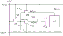
Fig. 2 shows a specific example of the pixel 10 in the mth column, nth row to (n + 2) th row (m, n are natural numbers equal to or greater than 1) of the pixel array.
The pixel 10 may employ a structure including a transistor 101, a transistor 102, a transistor 103, a transistor 104, a capacitor 105, a capacitor 106, and a circuit block 110. The circuit block 110 may include transistors, capacitors, display elements, and the like, and details thereof will be described later.
One of a source and a drain of the transistor 101 is electrically connected to one electrode of the capacitor 105. One electrode of the capacitor 105 is electrically connected to one of a source and a drain of the transistor 102. The other of the source and the drain of the transistor 102 is electrically connected to one of the source and the drain of the transistor 103. One of a source and a drain of the transistor 103 is electrically connected to one electrode of the capacitor 106. The other electrode of the capacitor 106 is electrically connected to one of the source and the drain of the transistor 104. One of a source and a drain of the transistor 104 is electrically connected to the circuit block 110.
Here, a wiring connecting one of the source and the drain of the transistor 104, the other electrode of the capacitor 106, and the circuit block is set as the node NM. The display elements included in the circuit block 110 operate according to the potential of the node NM. In addition, the node NM may be in a floating state by the constituent elements of the circuit block 110 connected to the node NM.
In addition, a wiring connecting one of the source and the drain of the transistor 101, one electrode of the capacitor 105, and one of the source and the drain of the transistor 102 is set as a node NA. Further, a wiring connecting the other of the source and the drain of the transistor 102, one electrode of the capacitor 106, and one of the source and the drain of the transistor 103 is set as a node NB.
Note that the storage unit M1 in fig. 1 corresponds to the node NM and its surrounding components. The storage unit M2 in fig. 1 corresponds to the node NA and its surrounding components. In addition, the display element 11 in fig. 1 is one of the components included in the circuit block 110.
Pixels 10[ n, m ] in the nth row]In the above description, the gate of the transistor 101, the gate of the transistor 103, and the gate of the transistor 104 are connected to the wiring 121[ n ]]And (6) electrically connecting. Gate of transistor 102 and wiring 121[ n +1]]And (6) electrically connecting. The other of the source and the drain of the transistor 101 and the other of the source and the drain of the transistor 104 are connected to a wiring 125[ m ]]And (6) electrically connecting. The other of the source and the drain of the transistor 103 is connected to a transistor capable of supplying a specific potential "Vref"are electrically connected. The other electrode of the capacitor 105 is connected to a capacitor capable of supplying a specific potential "Vr"are electrically connected.
In addition, the pixel 10[ n +1, m ] at the n +1 th row]In the above description, the gate of the transistor 101, the gate of the transistor 103, and the gate of the transistor 104 are connected to the wiring 121[ n +1]]And (6) electrically connecting. Gate of transistor 102 and wiring 121[ n + 2]]And (6) electrically connecting. The other of the source and the drain of the transistor 101 and the other of the source and the drain of the transistor 104 are connected to a wiring 125[ m ]]And (6) electrically connecting. The other of the source and the drain of the transistor 103 is connected to a transistor capable of supplying a specific potential "Vref"are electrically connected. The other electrode of the capacitor 105 is connected to a capacitor capable of supplying a specific potential "Vr"are electrically connected.
The wiring 121 is used as a gate line and is electrically connected to the gate driver 13 (see fig. 1). The wiring 125 is used as a source line and electrically connected to the source driver 12 (see fig. 1).
As described above, the gate line (the wiring 121) is electrically connected to two pixels 10 adjacent in the vertical direction. This enables parallel operation of two pixels 10 in the vertical direction.
As being able to supply "Vref'and' VrFor example, a power supply line electrically connected to the components of the circuit block 110 may be used as the wiring. In addition, can supply "Vref'and' Vr"may be the same or different.
The node NM, the node NA, and the node NB are used as storage nodes. By turning on the transistor connected to each node, data can be written to each node. Further, by making the transistor non-conductive, the data can be held in each node. By using a transistor with extremely low off-state current as the transistor, leakage current can be suppressed, and thus the potential of each node can be held for a long time. The transistor can be a transistor including a metal oxide in a channel formation region (hereinafter, an OS transistor), for example.
Specifically, as the transistors 101, 102, 103, and 104, OS transistors are preferably used. Further, an OS transistor may be used for the constituent elements included in the circuit block 110. In addition, when operation is performed within a range in which the amount of leakage current is allowable, a transistor including Si in a channel formation region (hereinafter, Si transistor) may be used. Further, an OS transistor and an Si transistor may be used in combination. Examples of the Si transistor include a transistor containing amorphous silicon, a transistor containing crystalline silicon (typically, low-temperature polysilicon or single crystal silicon), and the like.
As a semiconductor material used for the OS transistor, a metal oxide having an energy gap of 2eV or more, preferably 2.5eV or more, and more preferably 3eV or more can be used. Typically, an Oxide Semiconductor containing indium or the like is used, and for example, CAAC-OS (C-Axis Aligned crystal Oxide Semiconductor) or CAC (Cloud-Aligned Composite) -OS or the like, which will be mentioned later, can be used. CAAC-OS is suitable for transistors where the atoms constituting the crystal are stable and reliability is important. The CAC-OS exhibits high mobility characteristics and is suitable for a transistor or the like which performs high-speed driving.
Since the OS transistor has a large energy gap, it exhibits extremely low off-state current characteristics of only a few yA/μm (a current value of 1 μm per channel width). Unlike the Si transistor, the OS transistor has a characteristic of not causing impact ionization, avalanche breakdown, short channel effect, or the like, and thus can form a highly reliable circuit. In addition, variations in electrical characteristics due to non-uniformity in crystallinity caused by Si transistors are not easily generated in OS transistors.
As the semiconductor layer In the OS transistor, for example, a film represented by "In-M-Zn based oxide" containing indium, zinc, and M (a metal such as aluminum, titanium, gallium, germanium, yttrium, zirconium, lanthanum, cerium, tin, neodymium, or hafnium) can be used.
When the oxide semiconductor constituting the semiconductor layer is an In-M-Zn based oxide, the atomic ratio of the metal elements of the sputtering target for forming the In-M-Zn oxide film preferably satisfies in.gtoreq.M and Zn.gtoreq.M. The atomic ratio of the metal elements of such a sputtering target is preferably In: m: 1, Zn: 1: 1. in: m: 1, Zn: 1: 1.2, In: m: zn is 3: 1: 2. in: m: zn is 4: 2: 3. in: m: zn is 4: 2: 4.1, In: m: zn is 5: 1: 6. in: m: zn is 5: 1: 7. in: m: zn is 5: 1: 8, and the like. Note that the atomic ratio of the semiconductor layers formed may vary within a range of ± 40% of the atomic ratio of the metal element in the sputtering target.
As the semiconductor layer, an oxide semiconductor having a low carrier density is used. For example, a semiconductor layer having a carrier density of 1 × 10 can be used17/cm3Hereinafter, it is preferably 1 × 10¹⁵/cm3Hereinafter, more preferably 1 × 10¹³/cm3Hereinafter, more preferably 1 × 10¹¹/cm3Hereinafter, more preferably less than 1 × 10¹⁰/cm3And is 1X 10⁻⁹/cm3The oxide semiconductor described above. Such an oxide semiconductor is referred to as an oxide semiconductor which is intrinsic to high purity or substantially intrinsic to high purity. Since the oxide semiconductor has a low defect state density, it can be said to be an oxide semiconductor having stable characteristics.
Note that the present invention is not limited to the above description, and a material having an appropriate composition may be used in accordance with the semiconductor characteristics and the electrical characteristics (field effect mobility, threshold voltage, and the like) of a transistor which are required. In addition, it is preferable to appropriately set the carrier density, the impurity concentration, the defect density, the atomic ratio of the metal element to oxygen, the interatomic distance, the density, and the like of the semiconductor layer so as to obtain desired semiconductor characteristics of the transistor.
When the oxide semiconductor constituting the semiconductor layer contains silicon or carbon which is one of group 14 elements, oxygen vacancies increase to change the semiconductor layer to an n-type. Therefore, the concentration of silicon or carbon in the semiconductor layer (concentration measured by Secondary Ion Mass Spectrometry (SIMS)) is set to 2X 10¹⁸atoms/cm3Hereinafter, 2 × 10 is preferable17atoms/cm3The following.
In addition, when an alkali metal or an alkaline earth metal is bonded to an oxide semiconductor, carriers are generated, and an off-state current of a transistor may increase. Therefore, the concentration of the alkali metal or alkaline earth metal (concentration measured by SIMS) in the semiconductor layer is set to 1 × 10¹⁸atoms/cm3Hereinafter, 2 × 10 is preferable16atoms/cm3The following.
When the oxide semiconductor constituting the semiconductor layer contains nitrogen, electrons as carriers are generated, and the carrier density increases, so that the semiconductor layer is likely to be n-type. As a result, a transistor using an oxide semiconductor containing nitrogen easily has a normally-on characteristic. Therefore, the nitrogen concentration (concentration measured by SIMS) in the semiconductor layer is preferably 5 × 10¹⁸atoms/cm3The following.
In addition, when the oxide semiconductor constituting the semiconductor layer contains hydrogen, the hydrogen reacts with oxygen bonded to a metal atom to generate water, and therefore an oxygen vacancy is sometimes formed in the oxide semiconductor. In the case where a channel formation region in an oxide semiconductor contains oxygen vacancies, a transistor tends to have a normally-on characteristic. Further, a defect in which hydrogen enters an oxygen vacancy may be used as a donor to generate an electron as a carrier. In addition, a part of hydrogen is bonded to oxygen bonded to a metal atom, and electrons as carriers are generated in some cases. Therefore, a transistor using an oxide semiconductor containing a large amount of hydrogen easily has a normally-on characteristic.
The defect of hydrogen into the oxygen vacancy may be used as a donor of the oxide semiconductor. However, it is difficult to quantitatively evaluate the defect. Therefore, in an oxide semiconductor, evaluation may be performed not by a donor concentration but by a carrier concentration. Thus, in this specification and the like, as a parameter of the oxide semiconductor, a carrier concentration in a state where an electric field is not applied may be used instead of the donor concentration. That is, the "carrier concentration" described in this specification and the like may be referred to as "donor concentration".
Thus, it is preferable to reduce hydrogen in the oxide semiconductor as much as possible. Specifically, in the oxide semiconductor, the hydrogen concentration measured by SIMS is less than 1 × 10²⁰atoms/cm3Preferably less than 1X 10¹⁹atoms/cm3More preferably less than 5X 10¹⁸atoms/cm3More preferably less than 1X 10¹⁸atoms/cm3. By using an oxide semiconductor in which impurities such as hydrogen are sufficiently reduced in a channel formation region of a transistor, stable electrical characteristics can be provided.
The semiconductor layer may have a non-single crystal structure. The non-single crystal structure includes, for example, CAAC-OS having a crystal with c-axis orientation, a polycrystalline structure, a microcrystalline structure, or an amorphous structure. In the non-single crystalline structure, the defect state density is highest in the amorphous structure, and is lowest in the CAAC-OS.
The oxide semiconductor film having an amorphous structure has, for example, disordered atomic arrangement and has no crystalline component. Alternatively, the oxide film having an amorphous structure has, for example, a completely amorphous structure and does not have a crystal portion.
The semiconductor layer may be a mixed film of two or more kinds selected from a region having an amorphous structure, a region having a microcrystalline structure, a region having a polycrystalline structure, a region having CAAC-OS, and a region having a single crystal structure. The hybrid film sometimes has, for example, a single-layer structure or a laminated structure including two or more of the above-described regions.
The structure of CAC-OS, which is one embodiment of a non-single crystal semiconductor layer, will be described below.
The CAC-OS is, for example, a structure in which elements contained in an oxide semiconductor are unevenly distributed, and the size of a material containing the unevenly distributed elements is 0.5nm or more and 10nm or less, preferably 1nm or more and 2nm or less or an approximate size. Note that a state in which one or more metal elements are unevenly distributed in the oxide semiconductor and a region including the metal elements is mixed in a size of 0.5nm or more and 10nm or less, preferably 1nm or more and 2nm or less, or approximately, is also referred to as a mosaic (mosaic) shape or a patch (patch) shape in the following.
The oxide semiconductor preferably contains at least indium. In particular, indium and zinc are preferably contained. In addition, one or more selected from aluminum, gallium, yttrium, copper, vanadium, beryllium, boron, silicon, titanium, iron, nickel, germanium, zirconium, molybdenum, lanthanum, cerium, neodymium, hafnium, tantalum, tungsten, magnesium, and the like may be contained.
For example, CAC-OS among In-Ga-Zn oxides (In CAC-OS, In-Ga-Zn oxide may be particularly referred to as CAC-IGZO) means that the material is divided into indium oxide (hereinafter, referred to as InO)X1(X1 is a real number greater than 0)) or indium zinc oxide (hereinafter, referred to as In)X2ZnY2OZ2(X2, Y2, and Z2 are real numbers greater than 0)) and gallium oxide (hereinafter referred to as GaO)X3(X3 is a real number greater than 0)) or gallium zinc oxide (hereinafter referred to as GaX4ZnY4OZ4(X4, Y4, and Z4 are real numbers greater than 0)), and the like, and the mosaic-shaped InOX1Or InX2ZnY2OZ2A structure uniformly distributed in the film (hereinafter, also referred to as a cloud).
In other words, the CAC-OS is of GaOX3A region containing as a main component InX2ZnY2OZ2Or InOX1A composite oxide semiconductor having a structure in which regions that are main components are mixed together. In this specification, for example, when the atomic ratio of In to the element M In the first region is larger than the atomic ratio of In to the element M In the second region, the In concentration In the first region is higher than that In the second region.
Note that IGZO is generic and sometimes referred to asA compound containing In, Ga, Zn and O. A typical example is InGaO3(ZnO)m1(m1 is a natural number) or In(1+x0)Ga(1-x0)O3(ZnO)m0A crystalline compound represented by (-1. ltoreq. x 0. ltoreq.1, m0 is an arbitrary number).
The crystalline compound has a single crystal structure, a polycrystalline structure, or a CAAC structure. The CAAC structure is a crystal structure in which a plurality of IGZO nanocrystals have c-axis orientation and are connected in a non-oriented manner on the a-b plane.
On the other hand, CAC-OS is related to the material composition of an oxide semiconductor. CAC-OS refers to the following composition: in the material composition containing In, Ga, Zn, and O, some of the nanoparticle-like regions containing Ga as a main component and some of the nanoparticle-like regions containing In as a main component were observed to be irregularly dispersed In a mosaic shape. Therefore, in CAC-OS, the crystal structure is a secondary factor.
The CAC-OS does not contain a laminate structure of two or more films different in composition. For example, a structure composed of two layers of a film containing In as a main component and a film containing Ga as a main component is not included.
Note that GaO is sometimes not observedX3A region containing as a main component InX2ZnY2OZ2Or InOX1Is a well-defined boundary between regions of major composition.
In the case where the CAC-OS contains one or more selected from aluminum, yttrium, copper, vanadium, beryllium, boron, silicon, titanium, iron, nickel, germanium, zirconium, molybdenum, lanthanum, cerium, neodymium, hafnium, tantalum, tungsten, magnesium, and the like in place of gallium, the CAC-OS means a constitution as follows: some of the nano-particle-like regions containing the metal element as a main component and some of the nano-particle-like regions containing In as a main component were observed to be irregularly dispersed In a mosaic shape.
The CAC-OS can be formed by, for example, sputtering without intentionally heating the substrate. In the case of forming the CAC-OS by the sputtering method, as the film forming gas, one or more selected from an inert gas (typically argon), an oxygen gas, and a nitrogen gas may be used. The lower the flow ratio of the oxygen gas in the total flow of the film forming gas at the time of film formation, the better, for example, the flow ratio of the oxygen gas is set to 0% or more and less than 30%, preferably 0% or more and 10% or less.
The CAC-OS has the following characteristics: no clear peak was observed when measured by the Out-of-plane method according to one of the X-ray diffraction (XRD: X-ray diffraction) measurements using a theta/2 theta scan. That is, it was found that the orientation in the a-b plane direction and the c-axis direction was not present in the measurement region by the X-ray diffraction measurement.
In the electron diffraction pattern of CAC-OS obtained by irradiating an electron beam (also referred to as a nanobeam) having a beam diameter of 1nm, an annular region having high brightness (annular region) and a plurality of bright spots in the annular region were observed. From this, it is known that the crystal structure of CAC-OS has an nc (nanocrystalline) structure having no orientation in the plane direction and the cross-sectional direction, based on the electron diffraction pattern.
In addition, for example, In the CAC-OS of In-Ga-Zn oxide, it was confirmed that, based on an EDX plane analysis image obtained by Energy Dispersive X-ray spectrometry (EDX: Energy Dispersive X-ray spectroscopy): with GaOX3A region containing as a main component and InX2ZnY2OZ2Or InOX1The main component region is unevenly distributed and mixed.
The CAC-OS has a structure different from that of an IGZO compound in which metal elements are uniformly distributed, and has properties different from those of the IGZO compound. In other words, CAC-OS has a GaOX3Etc. as main component and InX2ZnY2OZ2Or InOX1The regions having the main components are separated from each other, and the regions having the elements as the main components are formed in a mosaic shape.
In here, InX2ZnY2OZ2Or InOX1The conductivity of the region having the main component is higher than that of GaOX3Etc. as the main component. In other words, when carriers flow InX2ZnY2OZ2Or InOX1When it is a region of main component, it is an oxide semiconductorIs used for the electrical conductivity of (1). Therefore, when In is usedX2ZnY2OZ2Or InOX1When the region as a main component is distributed in a cloud shape in the oxide semiconductor, high field-effect mobility (μ) can be achieved.
On the other hand, with GaOX3The insulating property of the region containing the above-mentioned component is higher than that of InX2ZnY2OZ2Or InOX1Is the region of the main component. In other words, when GaO is usedX3When the region containing the main component is distributed in the oxide semiconductor, leakage current can be suppressed, and a good switching operation can be achieved.
Therefore, when CAC-OS is used for the semiconductor element, the heat radiation is caused by GaOX3Insulation property of the like and the cause of InX2ZnY2OZ2Or InOX1Can realize high-current (I)on) And high field effect mobility (μ).
In addition, the semiconductor element using the CAC-OS has high reliability. Therefore, CAC-OS is suitable for constituent materials of various semiconductor devices.
The pixel 10 may have the structure shown in fig. 3A and 3B. Fig. 3A shows an example in which the other of the source and the drain of the transistor 104 is connected to one of the source and the drain of the transistor 101. Fig. 3B shows an example in which the other of the source and the drain of the transistor 101 is connected to one of the source and the drain of the transistor 104. Each of the structures can perform the same operation as the structure of fig. 2.
In addition, since capacitive coupling is used for the addition operation of the pixel 10, it is preferable to increase the capacitance value of the capacitor 105 provided on the supply side. On the other hand, in order to increase the aperture ratio of the pixel, it is preferable to make the occupied area of the capacitor as small as possible. Therefore, a structure in which capacitors are shared among pixels may be employed.
In the pixel 10 in which a new writing operation is not performed, the display operation is not affected even if the potential written to the capacitor 105 is changed. Therefore, the capacitor 105 can be shared among a plurality of pixels 10 to increase the capacitance. Note that the pixels 10 capable of sharing the capacitor 105 are limited to the pixels 10 that do not operate in parallel.
For example, as shown in fig. 4, a connection line 136 may be provided, whereby the capacitors 105 in every other pixel 10 in the vertical direction may be electrically connected in parallel. Although fig. 4 shows a structure in which two pixels 10 share the capacitor 105, three or more pixels 10 may share the capacitor 105 as long as every other pixel 10 in the vertical direction.
An example of the operation of adding the image data supplied to the pixel 10 will be described with reference to the timing chart shown in fig. 5. Note that in the following description, a high potential is denoted by "H" and a low potential is denoted by "L". Further, image data supplied when writing to the pixels of the first row, image data supplied when writing to the pixels of the second row, and image data supplied when writing to the pixels of the third row are "D1", "D2", and "D3", respectively. As a "Vref", for example, a potential of 0V, GND or a specific reference potential may be used.
First, the operation of writing "D1" to the node NA [ n, m ] and the node NM [ n, m ] of the pixel 10[ n, m ] in the nth row will be described. Note that, here, detailed changes due to the configuration, operation timing, and the like of the circuit are not considered in the distribution, coupling, or loss of the potential. The potential variation caused by the capacitive coupling depends on the capacitance ratio of the supply side and the supplied side, but for convenience of explanation, it is assumed that the capacitance value of the circuit block 110 is sufficiently small.
At time T1, the wiring 121[ n ] is connected]Is "H", thereby providing a pixel 10n, m with a high potential]In (1), the transistor 103 is turned on, and the potential of one electrode of the capacitor 106 becomes "Vref". This operation is a reset operation for performing the subsequent addition operation (capacitive coupling operation). Further, the transistor 101 is turned on, and the wiring 125[ m ]]Is written to the node NA n, m]. In addition, the transistor 104 is turned on, and the wiring 125[ m ]]Is written to the node NM [ n, m ]]. The job is a writing job of image data, and the node NA [ n, m ]]And node NM [ n, m ]]Becomes "D1".
At time T2, the wiring 121[ n ] is connected]Is "L", whereby the transistor 101, the transistor 103, and the transistor 104 are turned off. At this time, at node NA [ n, m ]]And sectionPoint NM [ n, m ]]While maintaining "D1". In addition, "D1-V" is held in the capacitor 106ref”。
This concludes the writing operation of "D1" in the pixel 10[ n, m ]. Next, an operation of adding "D1" in the pixel 10[ n, m ] and an operation of writing "D2" in the pixel 10[ n +1, m ] will be described.
At time T2, the wiring 121[ n +1]]Is "H", thereby providing a pixel 10n, m with a high potential]In (1), transistor 102 is turned on and held at node NA [ n, m ]]"D1" in (1) is read out to the node NB [ n, m]. At this time, node NB [ n, m ] is coupled by the capacitance of capacitor 106]Is added to the node NM [ n, m ] at a potential "D1]The potential of (2). The work being additive work, the nodes NM [ n, m ]]Becomes "D1-Vref+ D1 ". At this time, at "VrefWhen "is 0, the node NM [ n, m ]]Becomes "D1 + D1". That is, the node NA n, m may be held in the pair first]And node NM [ n, m ]]The data in (1) is added.
At pixel 10[ n +1, m]In (1), the transistor 103 is turned on, and the potential of one electrode of the capacitor 106 becomes "Vref". Further, the transistor 101 is turned on, and the wiring 125[ m ]]Is written to the node NA n +1, m]. In addition, the transistor 104 is turned on, and the wiring 125[ m ]]Is written to the node NM [ n +1, m ]]. The job is a writing job of image data, and the node NA [ n +1, m ]]And node NM [ n +1, m]Becomes "D2".
This operation is the addition operation of "D1" in the pixel 10[ n, m ] and the write operation of "D2" in the pixel 10[ n +1, m ]. Next, an operation of adding "D2" in the pixel 10[ n +1, m ] and an operation of writing "D3" in the pixel 10[ n +2, m ] will be described.
At time T3, the wiring 121[ n + 2]]Is "H", thereby providing a pixel 10[ n +1, m]In (1), transistor 102 is turned on and held at node NA n +1, m]"D2" in (1) is read to NB [ n +1, m]. At this time, node NB [ n +1, m ] is coupled by the capacitance of capacitor 106]Is added to the node NM [ n +1, m ]]The potential of (2). The work is additive, node NM [ n +1, m ]]Becomes "D2-Vref+ D2 ". At this time, at "VrefWhen "is 0, the node NMn+ 1,m]Becomes "D2 + D2".
At pixel 10[ n +2, m]In (1), the transistor 103 is turned on, and the potential of one electrode of the capacitor 106 becomes "Vref". Further, the transistor 101 is turned on, and the wiring 125[ m ]]Is written to the node NA n +2, m]. In addition, the transistor 104 is turned on, and the wiring 125[ m ]]Is written to the node NM [ n +2, m ]]. The job is a writing job of image data, and the node NA [ n +2, m ]]And node NM [ n +2, m]Becomes "D3".
This operation is the addition operation of "D2" in the pixel 10[ n +1, m ] and the write operation of "D3" in the pixel 10[ n +2, m ]. In the pixel 10[ n +2, m ], the same operation as described above is performed based on the timing chart shown in fig. 5, whereby the addition operation of "D3" can be performed.
As described above, one embodiment of the present invention can perform an operation for adding two pieces of image data. By adding the image data, a potential equal to or higher than the maximum output voltage of the source driver can be supplied to the display element, which contributes to improvement of display luminance, expansion of a dynamic range, and the like. In addition, when a standard display is performed, the output voltage of the source driver can be reduced to about 1/2, whereby power consumption can be reduced.
In addition, since the writing operation of the image data in the pixel of the n-th row and the addition operation of the image data in the pixel of the n + 1-th row can be performed in parallel, the frame rate can be improved. This makes it easy to increase the frame rate even when the horizontal period is shortened due to an increase in the number of pixels. In addition, one embodiment of the present invention is applied to a field sequential liquid crystal display device which needs to operate at high speed.
Fig. 6A to 6C are examples of a structure which can be used for the circuit block 110 and includes an EL element as a display element.
The structure shown in fig. 6A includes a transistor 111, a capacitor 113, and an EL element 114. One of a source and a drain of the transistor 111 is electrically connected to one electrode of the EL element 114. One electrode of the EL element 114 is electrically connected to one electrode of the capacitor 113. The other electrode of the capacitor 113 is electrically connected to the gate of the transistor 111. The gate of the transistor 111 is electrically connected to the node NM.
The other of the source and the drain of the transistor 111 is electrically connected to the wiring 128. The other electrode of the EL element 114 is electrically connected to a wiring 129. The wirings 128 and 129 have a function of supplying power. For example, the wiring 128 may supply a high potential power supply. In addition, the wiring 129 can supply a low potential power source.
Here, the wiring 128 may be used for supplying "V" as shown in FIG. 1ref"is used. In addition, the wiring 128 may also be used for supplying "Vr"is used. Because of "VrefAnd Vr"0V, GND or a low potential is preferable, so the wiring 128 also has a function of supplying at least any one of these potentials. For the wiring 128, "V" is supplied at the timing of writing data to the node NMrefAnd Vr", a high potential power source may be supplied at a timing when the EL element 114 emits light. In addition, a dedicated supply "V" may be providedref'and' Vr"is common wiring.
In the structure shown in fig. 6A, when the potential of the node NM becomes equal to or higher than the threshold voltage of the transistor 111, a current flows through the EL element 114. This may cause the EL element 114 to start emitting light at the stage of writing of image data shown in the timing chart of fig. 5, and thus the application of this configuration may be limited.
Fig. 6B is a structure in which a transistor 112 is added to the structure of fig. 6A. One of a source and a drain of the transistor 112 is electrically connected to one of a source and a drain of the transistor 111. The other of the source and the drain of the transistor 112 is electrically connected to the EL element 114. A gate of the transistor 112 is electrically connected to a wiring 127. The wiring 127 may have a function of a signal line which controls conduction of the transistor 112.
In this structure, when the potential of the node NM is equal to or higher than the threshold voltage of the transistor 111 and the transistor 112 is on, a current flows through the EL element 114. Therefore, light emission of the EL element 114 can be started after the second writing shown in the timing chart of fig. 3.
Fig. 6C is a structure in which a transistor 115 is added to the structure of fig. 6B. One of a source and a drain of the transistor 115 is electrically connected to one of a source and a drain of the transistor 111. The other of the source and the drain of the transistor 115 is electrically connected to the wiring 130. A gate of the transistor 115 is electrically connected to the wiring 131. The wiring 131 may have a function of a signal line which controls conduction of the transistor 115.
The wiring 130 may be electrically connected to a source for supplying a specific potential such as a reference potential. Writing of image data can also be stabilized by supplying a specific potential from the wiring 130 to one of the source and the drain of the transistor 111.
In addition, the wiring 130 may be connected to the circuit 120, and may have a function of a monitor line. The circuit 120 may have one or more of a function of supplying the specific potential, a function of acquiring electrical characteristics of the transistor 111, and a function of generating correction data.
Fig. 7A to 7C are examples of structures that can be used for the circuit block 110 and include a liquid crystal element as a display element.
The structure shown in fig. 7A includes a capacitor 116 and a liquid crystal element 117. One electrode of the liquid crystal element 117 is electrically connected to one electrode of the capacitor 116. One electrode of the capacitor 116 is electrically connected to the node NM.
The other electrode of the capacitor 116 is electrically connected to the wiring 132. The other electrode of the liquid crystal element 117 is electrically connected to the wiring 133. The wirings 132 and 133 have a function of supplying power. For example, the wirings 132 and 133 can supply reference potentials such as GND and 0V or arbitrary potentials.
Here, the wiring 132 may be used for supplying "V" as shown in FIG. 1ref"is used. In addition, the wiring 132 may be used for supplying "Vr"is used. In addition, a dedicated supply "V" may be providedref'and' Vr"is common wiring.
In this configuration, the operation of the liquid crystal element 117 is started when the potential of the node NM is equal to or higher than the operation threshold of the liquid crystal element 117. Therefore, the display operation may be started at the stage of writing of image data shown in the timing chart of fig. 5, and thus the application of this configuration may be limited. Note that in the case of the transmissive liquid crystal display device, by further performing an operation such as turning off the backlight until the end of the operation of adding image data shown in the timing chart of fig. 5, it is possible to suppress an unnecessary display operation from being visible.
Fig. 7B is a structure in which a transistor 118 is added to the structure of fig. 7A. One of a source and a drain of the transistor 118 is electrically connected to one electrode of the capacitor 116. The other of the source and the drain of the transistor 118 is electrically connected to the node NM. A gate of the transistor 118 is electrically connected to a wiring 127. The wiring 127 may have a function of a signal line which controls conduction of the transistor 118.
In this structure, the potential of the node NM is applied to the liquid crystal element 117 while the transistor 118 is turned on. This makes it possible to start the operation of the liquid crystal element after the operation of adding the image data in the timing chart shown in fig. 5.
Further, since the potential supplied to the capacitor 116 and the liquid crystal element 117 is continuously held in a state where the transistor 118 is turned off, it is preferable to reset the potential supplied to the capacitor 116 and the liquid crystal element 117 before rewriting image data. In this reset, for example, a reset potential may be supplied to a source line (a wiring 125 shown in fig. 2) connected to a pixel, and the transistor 103 and the transistor 118 may be turned on at the same time.
Fig. 7C is a structure in which a transistor 119 is added to the structure of fig. 7B. One of a source and a drain of the transistor 119 is electrically connected to one electrode of the liquid crystal element 117. The other of the source and the drain of the transistor 119 is electrically connected to the wiring 130. A gate of the transistor 119 is electrically connected to the wiring 131. The wiring 131 can function as a signal line which controls conduction of the transistor 119.
The circuit 120 electrically connected to the wiring 130 may have a function of resetting a potential supplied to the capacitor 116 and the liquid crystal element 117, similarly to the above-described description of fig. 6C.
Further, although fig. 6, 7 show that "V" is supplied from the power supply lineref"however," V "may be supplied from a gate lineref". For example, as shown in FIG. 8A, at pixel 10[ n, m ]]May also be supplied with "V" from the wiring 121ref". As shown in the timing diagram of fig. 5, because during writingWhen the transistor 103 is turned on, "D1" (D1) ", the wiring 121 is n +1, m]Is supplied with a potential equivalent to "L", so that the potential can be used as "V"ref”。
As shown in fig. 8B and 8C, the transistors 101, 102, 103, and 104 may have a structure in which a back gate is provided. Fig. 8B shows a structure in which a back gate is electrically connected to a front gate, which has an effect of increasing an on-state current. Fig. 8C shows a structure in which a back gate is electrically connected to a wiring 134 capable of supplying a constant potential, which can control the threshold voltage of a transistor. In addition, the back gate may be provided in the transistors included in the circuit block 110 shown in fig. 6A to 6C and fig. 7A to 7C.
Next, a simulation result of applying the circuit block shown in fig. 7A to the structure of the pixel 10 of the display device shown in fig. 2 (see fig. 9A) will be described. The parameters are as follows: the transistor size is 4 μm/40 μm (the transistor included in the pixel 10); the capacitance values of the capacitors C1 and C2 are 5pF, and the capacitance value of the capacitor Cs is 500 fF; the capacitance value of the liquid crystal cell Clc is 1 pF; the image DATA (DATA) is 5V at maximum, "Vref”、“Vr"is 0V, and the common electrodes CsCOM and TCOM are 0V. Further, "H" is set to +20V and "L" is set to-20V as a voltage applied to the gate of the transistor. Note that SPICE was used as the circuit simulation software.
Fig. 10 shows simulation results when the circuit shown in fig. 9A is operated according to the timing chart shown in fig. 9B.
Fig. 10 is a simulation result of voltages in the node NM [ n ] and the node NM [ n +1] when +5V is input as the image DATA (DATA). At the node NM [ n ], the first writing is performed at a timing at which GL [ n ] becomes "H", and the second writing is performed at a timing at which GL [ n +1] becomes "H", and it is confirmed that the image DATA (DATA) is added according to the capacitance ratio between the supply side and the supplied side. The same applies to node NM [ n +1 ].
Fig. 11 is a simulation result of voltages in the node NM [ n ] and the node NM [ n +1] when-5V to +5V are input as image DATA (DATA). In any case, it was confirmed that the image DATA (DATA) was added according to the capacitance ratio of the supply side to the supplied side.
From the above simulation results, the following can be confirmed: the potentials held in the two nodes may be added to be supplied to the display element. The display device according to one embodiment of the present invention can also perform parallel operation in the vertical direction, and is preferably applied to a display device which needs high-speed operation.
This embodiment can be implemented in combination with the structures described in other embodiments and the like as appropriate.
(embodiment mode 2)
In this embodiment, a configuration example of a display device using a liquid crystal element and a configuration example of a display device using an EL element are described. Note that in this embodiment, the constituent elements, operations, and functions of the display device described in embodiment 1 are omitted.
Fig. 12A to 12C show a structure of a display device to which one embodiment of the present invention can be applied.
In fig. 12A, a sealant 4005 is provided so as to surround a display portion 215 provided over a first substrate 4001, and the display portion 215 is sealed by the sealant 4005 and a second substrate 4006.
The pixel 10 described in embodiment 1 and the like can be provided in the display portion 215. Note that a scanning line driver circuit described below corresponds to a gate driver, and a signal line driver circuit corresponds to a source driver.
In fig. 12A, the scanning line driver circuit 221a, the signal line driver circuit 231a, the signal line driver circuit 232A, and the common line driver circuit 241a each include a plurality of integrated circuits 4042 provided on a printed circuit board 4041. The integrated circuit 4042 is formed of a single crystal semiconductor or a polycrystalline semiconductor. The common line driver circuit 241a has a function of supplying a predetermined potential to the wirings 128, 129, 132, 133, and the like described in embodiment 1.
Various signals and potentials are supplied to the scanning line driver circuit 221a, the common line driver circuit 241a, the signal line driver circuit 231a, and the signal line driver circuit 232a through an FPC (Flexible printed circuit) 4018.
The integrated circuit 4042 included in the scanning line driver circuit 221a and the common line driver circuit 241a has a function of supplying a selection signal to the display portion 215. The integrated circuit 4042 included in the signal line driver circuit 231a and the signal line driver circuit 232a has a function of supplying image data to the display portion 215. An integrated circuit 4042 is mounted in a region different from a region surrounded by the sealant 4005 over the first substrate 4001.
Note that a connection method of the integrated circuit 4042 is not particularly limited, and a wire bonding method, a cog (chip On glass) method, a tcp (tape Carrier package) method, a cof (chip On film) method, or the like can be used.
Fig. 12B shows an example in which an integrated circuit 4042 included in the signal line driver circuit 231a and the signal line driver circuit 232a is mounted by the COG method. In addition, a system-on-panel (system-on-panel) can be formed by forming a part or the whole of the driver circuit over a substrate over which the display portion 215 is formed.
Fig. 12B shows an example in which the scanning line driver circuit 221a and the common line driver circuit 241a are formed over a substrate over which the display portion 215 is formed. By forming the driver circuit and the pixel circuit in the display portion 215 at the same time, the number of components can be reduced. Thereby, productivity can be improved.
In fig. 12B, a sealant 4005 is provided so as to surround the display portion 215, the scan line driver circuit 221a, and the common line driver circuit 241a provided over the first substrate 4001. The second substrate 4006 is provided over the display portion 215, the scan line driver circuit 221a, and the common line driver circuit 241 a. Thus, the display portion 215, the scan line driver circuit 221a, and the common line driver circuit 241a are sealed together with the display element by the first substrate 4001, the sealant 4005, and the second substrate 4006.
Although fig. 12B illustrates an example in which the signal line driver circuit 231a and the signal line driver circuit 232a are separately formed and mounted on the first substrate 4001, one embodiment of the present invention is not limited to this configuration, and a scan line driver circuit may be separately formed and mounted, or a part of the signal line driver circuit or a part of the scan line driver circuit may be separately formed and mounted. As shown in fig. 12C, the signal line driver circuit 231a and the signal line driver circuit 232a may be formed over a substrate over which the display portion 215 is formed.
Further, the display device may include a panel in which a display element is sealed, and a module in which an IC or the like including a controller is mounted on the panel.
In addition, the display portion and the scan line driver circuit provided over the first substrate include a plurality of transistors. As the transistor, the transistor described in the above embodiment mode can be used.
The transistors included in the peripheral driver circuit and the transistors included in the pixel circuit of the display portion may have the same structure or different structures. The transistors included in the peripheral driver circuit may all have the same structure, or two or more structures may be combined. Similarly, the transistors included in the pixel circuit may have the same structure, or two or more structures may be combined.
In addition, an input device 4200 may be provided over the second substrate 4006. The structure in which the input device 4200 is provided to the display device shown in fig. 12A to 12C can be used as a touch panel.
The sensing element (also referred to as a "sensing element") included in the touch panel according to one embodiment of the present invention is not particularly limited. Various sensors capable of detecting the approach or contact of a detection object such as a finger or a stylus pen can also be used as the sensing element.
As a sensor system, for example, various systems such as a capacitance type, a resistance film type, a surface acoustic wave type, an infrared type, an optical type, and a pressure-sensitive type can be used.
In this embodiment, a touch panel including a capacitance-type sensor element will be described as an example.
The capacitance type includes a surface type capacitance type, a projection type capacitance type, and the like. The projection type capacitance includes a self capacitance and a mutual capacitance. The use of mutual capacitance is preferred because multipoint sensing can be done simultaneously.
A touch panel according to one embodiment of the present invention can have various structures such as a structure in which a display device and a sensor element which are manufactured separately are bonded to each other, and a structure in which an electrode or the like constituting a sensor element is provided over one or both of a substrate supporting a display element and a counter substrate.
Fig. 13A and 13B illustrate an example of a touch panel. Fig. 13A is a perspective view of the touch panel 4210. Fig. 13B is a perspective view of the input device 4200. Note that only typical constituent elements are shown for clarity.
The touch screen 4210 has a structure in which a display device and a sensing element which are separately manufactured are attached.
The touch screen 4210 includes an input device 4200 and a display device which are disposed to overlap.
The input device 4200 includes a substrate 4263, an electrode 4227, an electrode 4228, a plurality of wirings 4237, a plurality of wirings 4238, and a plurality of wirings 4239. For example, the electrode 4227 may be electrically connected to the wiring 4237 or the wiring 4239. In addition, the electrode 4228 may be electrically connected to a wiring 4239. The FPC4272b can be electrically connected to each of the plurality of wirings 4237 and 4238. FPC4272b may be provided with IC4273 b.
Alternatively, a touch sensor may be provided between the first substrate 4001 and the second substrate 4006 of the display device. When a touch sensor is provided between the first substrate 4001 and the second substrate 4006, an optical touch sensor using a photoelectric conversion element can be used in addition to an electrostatic capacitance type touch sensor.
Fig. 14A and 14B are sectional views along the chain line N1-N2 in fig. 12B. The display device shown in fig. 14A and 14B includes an electrode 4015, and the electrode 4015 and a terminal of an FPC4018 are electrically connected through an anisotropic conductive layer 4019. In fig. 14A and 14B, an electrode 4015 is electrically connected to a wiring 4014 in an opening formed in the insulating layer 4112, the insulating layer 4111, and the insulating layer 4110.
The electrode 4015 and the first electrode layer 4030 are formed using the same conductive layer, and the wiring 4014 and source and drain electrodes of the transistor 4010 and the transistor 4011 are formed using the same conductive layer.
In addition, the display portion 215 and the scan line driver circuit 221a provided over the first substrate 4001 include a plurality of transistors, and fig. 14A and 14B illustrate a transistor 4010 in the display portion 215 and a transistor 4011 in the scan line driver circuit 221 a. Although a bottom-gate transistor is illustrated as the transistor 4010 and the transistor 4011 in fig. 14A and 14B, a top-gate transistor may be used.
In fig. 14A and 14B, an insulating layer 4112 is provided over the transistor 4010 and the transistor 4011. In addition, in fig. 14B, a partition 4510 is formed over the insulating layer 4112.
In addition, a transistor 4010 and a transistor 4011 are provided over the insulating layer 4102. In addition, the transistor 4010 and the transistor 4011 include an electrode 4017 formed over an insulating layer 4111. The electrode 4017 can be used as a back gate electrode.
In addition, the display device shown in fig. 14A and 14B includes a capacitor 4020. The capacitor 4020 includes an electrode 4021 formed in the same step as a gate electrode of the transistor 4010 and electrodes formed in the same step as source and drain electrodes. Each electrode overlaps with each other with an insulating layer 4103 interposed therebetween.
In general, the capacitance of a capacitor provided in a pixel portion of a display device is set so as to be able to hold electric charges for a predetermined period in consideration of a leakage current of a transistor arranged in the pixel portion or the like. The capacity of the capacitor may be set in consideration of the off-state current of the transistor.
The transistor 4010 provided in the display portion 215 is electrically connected to a display element. Fig. 14A shows an example of a liquid crystal display device in which a liquid crystal element is used as a display element. In fig. 14A, a liquid crystal element 4013 which is a display element includes a first electrode layer 4030, a second electrode layer 4031, and a liquid crystal layer 4008. Note that the insulating layers 4032 and 4033 which function as alignment films are provided so as to sandwich the liquid crystal layer 4008. The second electrode layer 4031 is provided on the second substrate 4006 side, and the first electrode layer 4030 and the second electrode layer 4031 overlap with each other with the liquid crystal layer 4008 interposed therebetween.
The spacer 4035 is a columnar spacer obtained by selectively etching an insulating layer, and is provided for controlling a space (cell gap) between the first electrode layer 4030 and the second electrode layer 4031. Note that a spherical spacer may also be used.
Further, as necessary, an optical member (optical substrate) such as a black matrix (light-shielding layer), a colored layer (color filter), a polarizing member, a phase difference member, and an antireflection member may be appropriately provided. For example, circular polarization using a polarizing substrate and a phase difference substrate may be used. Further, as the light source, a backlight, a side light, or the like may be used. As the backlight or side light, Micro-LEDs and the like may be used.
In the display device shown in fig. 14A, a light-shielding layer 4132, a colored layer 4131, and an insulating layer 4133 are provided between the second substrate 4006 and the second electrode layer 4031.
Examples of materials that can be used for the light-shielding layer include carbon black, titanium black, metals, metal oxides, and composite oxides containing a solid solution of a plurality of metal oxides. The light-shielding layer may be a film containing a resin material or a thin film containing an inorganic material such as a metal. Further, a laminated film of films including materials of the colored layers may be used for the light-shielding layer. For example, a stacked structure of a film including a material of a colored layer for transmitting light of a certain color and a film including a material of a colored layer for transmitting light of another color may be employed. It is preferable that the colored layer and the light-shielding layer are made of the same material because the process can be simplified, in addition to the use of the same equipment.
Examples of materials that can be used for the colored layer include metal materials, resin materials, and resin materials containing pigments or dyes. The light-shielding layer and the colored layer can be formed by, for example, an inkjet method.
In addition, the display device shown in fig. 14A and 14B includes an insulating layer 4111 and an insulating layer 4104. As the insulating layer 4111 and the insulating layer 4104, insulating layers which are less likely to transmit impurity elements are used. By sandwiching the semiconductor layer of the transistor between the insulating layer 4111 and the insulating layer 4104, impurities from the outside can be prevented from being mixed.
As a display element included in the display device, a light-emitting element (also referred to as an EL element) using electroluminescence can be applied. An EL element has a layer containing a light-emitting compound (also referred to as an EL layer) between a pair of electrodes. When a potential difference higher than the threshold voltage of the EL element is generated between the pair of electrodes, holes are injected into the EL layer from the anode side, and electrons are injected into the EL layer from the cathode side. The injected electrons and holes are recombined in the EL layer, whereby the light-emitting compound contained in the EL layer emits light.
The EL element is distinguished depending on whether the light emitting material is an organic compound or an inorganic compound, and generally the former is referred to as an organic EL element, and the latter is referred to as an inorganic EL element. Note that an LED (including Micro-LED) using a compound semiconductor as a light emitting material is also one of EL elements.
In an organic EL element, by applying a voltage, electrons are injected from one electrode into an EL layer, and holes are injected from the other electrode into the EL layer. These carriers (electrons and holes) are recombined to form an excited state of the light-emitting organic compound, and light is emitted when the light-emitting organic compound returns from the excited state to a ground state. Due to such a mechanism, such a light-emitting element is called a current excitation type light-emitting element.
The EL layer may contain a substance having a high hole-injecting property, a substance having a high hole-transporting property, a hole-blocking material, a substance having a high electron-transporting property, a substance having a high electron-injecting property, a bipolar substance (a substance having a high electron-transporting property and a high hole-transporting property), or the like in addition to the light-emitting compound.
The EL layer can be formed by a method such as a vapor deposition method (including a vacuum vapor deposition method), a transfer method, a printing method, an ink-jet method, or a coating method.
Inorganic EL elements are classified into dispersion-type inorganic EL elements and thin-film-type inorganic EL elements according to their element structures. A dispersion-type inorganic EL element includes a light-emitting layer in which particles of a light-emitting material are dispersed in a binder, and its light emission mechanism is donor-acceptor recombination-type light emission utilizing a donor level and an acceptor level. The thin film type inorganic EL element is a structure in which a light emitting layer is sandwiched between dielectric layers, and the dielectric layers sandwiching the light emitting layer are sandwiched between electrodes, and its light emission mechanism is localized type light emission utilizing inner shell electron transition of metal ions. Note that here, an organic EL element is used as a light-emitting element for description.
In order to extract light emission, at least one of the pair of electrodes of the light-emitting element may be transparent. A transistor and a light-emitting element are formed over a substrate, and a top emission structure which emits light from a surface on the opposite side of the substrate can be used as the light-emitting element; taking out a bottom emission structure emitting light from a surface of one side of the substrate; and a double-sided emission structure taking out light emission from both surfaces.
Fig. 14B shows an example of a light-emitting display device (also referred to as an "EL display device") using a light-emitting element as a display element. A light-emitting element 4513 which is used as a display element is electrically connected to a transistor 4010 provided in the display portion 215. Although the light-emitting element 4513 has a stacked-layer structure of the first electrode layer 4030, the light-emitting layer 4511, and the second electrode layer 4031, the structure is not limited to this. The structure of the light-emitting element 4513 can be changed as appropriate depending on the direction in which light is extracted from the light-emitting element 4513, and the like.
The partition wall 4510 is formed using an organic insulating material or an inorganic insulating material. In particular, it is preferable to form an opening in the first electrode layer 4030 using a photosensitive resin material, and to form a side surface of the opening as an inclined surface having a continuous curvature.
The light-emitting layer 4511 may be formed using one layer or a stack of a plurality of layers.
The light-emitting element 4513 may emit light of white, red, green, blue, cyan, magenta, yellow, or the like depending on a material constituting the light-emitting layer 4511.
As a method for realizing color display, there are the following methods: a method of combining the light-emitting element 4513 whose emission color is white and a colored layer; and a method of providing a light-emitting element 4513 which emits light of a different color for each pixel. The former method has higher productivity than the latter method. On the other hand, in the latter method, the light-emitting layer 4511 needs to be formed for each pixel, so that the productivity is lower than that in the former method. However, in the latter method, a higher emission color can be obtained than in the former method. In the latter method, the color purity can be further improved by providing the light-emitting element 4513 with a microcavity structure.
The light-emitting layer 4511 may contain an inorganic compound such as a quantum dot. For example, quantum dots can be used as a light-emitting material by using the quantum dots for a light-emitting layer.
In order to prevent oxygen, hydrogen, moisture, carbon dioxide, or the like from entering the light-emitting element 4513, a protective layer may be formed over the second electrode layer 4031 and the partition 4510. As the protective layer, silicon nitride oxide, aluminum nitride, aluminum oxynitride, aluminum nitride oxide, dlc (diamond Like carbon), or the Like can be formed. A space sealed by the first substrate 4001, the second substrate 4006, and the sealant 4005 is provided with a filler 4514 and sealed. In this way, it is preferable to seal (enclose) the package with a protective film (adhesive film, ultraviolet curable resin film, or the like) or a cover material having high airtightness and little outgassing so as not to be exposed to the outside air.
As the filler 4514, in addition to an inert gas such as nitrogen or argon, an ultraviolet-curable resin or a thermosetting resin may be used, and for example, PVC (polyvinyl chloride), an acrylic resin, polyimide, an epoxy resin, a silicone resin, PVB (polyvinyl butyral), EVA (ethylene vinyl acetate), or the like can be used. Filler 4514 may also contain a desiccant.
As the sealant 4005, a glass material such as glass frit, or a resin material such as a curable resin, a photocurable resin, or a thermosetting resin that is curable at room temperature such as a two-liquid mixture resin can be used. The sealant 4005 may also contain a desiccant.
Further, as necessary, an optical film such as a polarizing plate, a circularly polarizing plate (including an elliptically polarizing plate), a retardation plate (λ/4 plate, λ/2 plate), a color filter, or the like may be appropriately provided on the light emitting surface of the light emitting element. Further, an antireflection film may be provided on the polarizing plate or the circular polarizing plate. For example, anti-glare treatment for reducing reflection glare by diffusing reflected light using surface irregularities may be performed.
By providing the light-emitting element with a microcavity structure, light with high color purity can be extracted. In addition, by combining the microcavity structure and the color filter, reflection glare can be prevented, and visibility of an image can be improved.
The first electrode layer and the second electrode layer (also referred to as a pixel electrode layer, a common electrode layer, a counter electrode layer, or the like) which apply a voltage to the display element may have light transmittance or reflectance selected depending on the direction of light extraction, the place where the electrode layer is provided, and the pattern structure of the electrode layer.
As the first electrode layer 4030 and the second electrode layer 4031, a light-transmitting conductive material such as indium oxide containing tungsten oxide, indium zinc oxide containing tungsten oxide, indium oxide containing titanium oxide, indium tin oxide containing titanium oxide, indium zinc oxide, or indium tin oxide to which silicon oxide is added can be used.
The first electrode layer 4030 and the second electrode layer 4031 can be formed using one or more of metals such as tungsten (W), molybdenum (Mo), zirconium (Zr), hafnium (Hf), vanadium (V), niobium (Nb), tantalum (Ta), chromium (Cr), cobalt (Co), nickel (Ni), titanium (Ti), platinum (Pt), aluminum (Al), copper (Cu), and silver (Ag), alloys thereof, and nitrides thereof.
In addition, the first electrode layer 4030 and the second electrode layer 4031 can be formed using a conductive composition containing a conductive polymer (also referred to as a conductive polymer). As the conductive polymer, a so-called pi electron conjugated conductive polymer can be used. For example, polyaniline or a derivative thereof, polypyrrole or a derivative thereof, polythiophene or a derivative thereof, or a copolymer or a derivative thereof composed of two or more kinds of aniline, pyrrole, and thiophene can be given.
Further, since a transistor is easily broken by static electricity or the like, a protection circuit for protecting a driver circuit is preferably provided. The protection circuit is preferably formed using a nonlinear element.
Note that as shown in fig. 15, a stacked structure in which the transistor and the capacitor include an overlapping region in the height direction may be employed. For example, by disposing the transistor 4011 and the transistor 4022 which constitute the driver circuit so as to overlap with each other, a display device with a narrow frame can be realized. Further, by disposing the transistor 4010, the transistor 4023, the capacitor 4020, and the like which constitute the pixel circuit so as to partially include an overlapping region, the aperture ratio and the resolution can be improved. Fig. 15 shows an example in which the stacked structure is applied to the liquid crystal display device shown in fig. 14A, but the structure may be applied to the EL display device shown in fig. 14B.
In addition, in the pixel circuit, a light-transmitting conductive film having high light transmittance to visible light is used as an electrode and a wiring, and the light transmittance in the pixel can be increased, so that the aperture ratio can be substantially increased. Further, since the semiconductor layer also has light-transmitting properties when an OS transistor is used, the aperture ratio is further improved. This is also effective when a transistor or the like does not have a stacked structure.
Further, a display device may be configured by combining a liquid crystal display device and a light-emitting device.
The light emitting device is disposed on the opposite side of the display surface or at an end portion of the display surface. The light-emitting device has a function of supplying light to the display element. The light emitting device is called a backlight.
Here, the light-emitting device may include a plate-shaped or film-shaped light guide portion (also referred to as a light guide plate) and a plurality of light-emitting elements that emit light of different colors. By disposing the light emitting element near the side surface of the light guide portion, light can be emitted from the side surface of the light guide portion to the inside. The light guide portion includes a mechanism (also referred to as a light extraction mechanism) that changes an optical path, whereby the light emitting device can uniformly irradiate light to the pixel portion of the display panel. Alternatively, a light-emitting device may be disposed directly below a pixel without providing a light guide portion.
The light-emitting device preferably includes light-emitting elements of three colors of red (R), green (G), and blue (B). Further, a white (W) light-emitting element may be included. Light Emitting Diodes (LEDs) are preferably used as the Light emitting elements.
The light-emitting element preferably has an emission spectrum with a Full Width at half maximum (FWHM) of 50nm or less, preferably 40nm or less, more preferably 30nm or less, and still more preferably 20nm or less, and has a very high color purity. Note that the smaller the full width at half maximum of the emission spectrum, the better, and for example, 1nm or more may be used. Thus, when color display is performed, vivid display with high color reproducibility can be performed.
In addition, it is preferable to use a red light-emitting element having an emission spectrum with a peak wavelength in a range of 625nm to 650 nm. In addition, it is preferable to use a green light-emitting element having an emission spectrum with a peak wavelength in a range of 515nm to 540 nm. The blue light-emitting element preferably has an emission spectrum with a peak wavelength in a range of 445nm to 470 nm.
The display device sequentially flashes the light-emitting elements of three colors and simultaneously drives the pixels in synchronization with the flashing, thereby performing color display by a sequential additive color mixing method. This driving method may also be referred to as field sequential driving.
The field sequential driving can display vivid color images. In addition, a smooth moving image can be displayed. Further, by using the above driving method, since it is not necessary to configure one pixel by a plurality of sub-pixels of different colors, the effective reflection area (also referred to as effective display area, aperture ratio) of one pixel can be enlarged, and bright display can be performed. Further, since it is not necessary to provide a color filter in the pixel, the transmittance of the pixel can be increased, and brighter display can be performed. In addition, the manufacturing process can be simplified, and thus the manufacturing cost can be reduced.
Fig. 16A and 16B are schematic cross-sectional views of a display device capable of field sequential driving. A backlight unit capable of emitting light of each color of RGB is provided on the substrate 4001 side of the display device. Note that in the field sequential driving, since the display colors are emitted in time division of each color of RGB, a color filter is not necessary.
The backlight unit 4340a shown in fig. 16A has a structure in which a plurality of light-emitting elements 4342 are provided directly below a pixel with a diffuser plate 4352 interposed therebetween. The diffuser plate 4352 has a function of diffusing light emitted from the light-emitting element 4342 to the substrate 4001 side to make luminance uniform in the display portion surface. A polarizing plate may be provided between the light-emitting element 4342 and the diffusion plate 4352 as necessary. The diffusion plate 4352 may not be provided if it is not necessary. The light-shielding layer 4132 may be omitted.
In the backlight unit 4340a, a large number of light-emitting elements 4342 can be mounted, and thus bright display can be realized. Further, there is an advantage that a light guide plate is not necessary and the light efficiency of the light-emitting element 4342 is not easily lost. Note that a lens 4344 for light diffusion may be provided in the light-emitting element 4342 as needed.
The backlight unit 4340B shown in fig. 16B has a structure in which a light guide plate 4341 is provided directly below the pixel with a diffusion plate 4352 interposed therebetween. A plurality of light emitting elements 4342 are provided at an end of the light guide plate 4341. The light guide plate 4341 has a concave-convex shape on the side opposite to the diffusion plate 4352, and thus guided light can be scattered by the concave-convex shape and emitted in the direction of the diffusion plate 4352.
The light-emitting element 4342 may be fixed to the printed circuit board 4347. Note that, although fig. 16B shows that the light-emitting elements 4342 of RGB colors overlap each other, the light-emitting elements 4342 of RGB colors may be arranged in the depth direction. A reflective layer 4348 that reflects visible light may be provided on the light guide plate 4341 on the side opposite to the light-emitting element 4342.
The backlight unit 4340b can reduce the number of light-emitting elements 4342, and thus can realize a low-cost and thin backlight unit.
A light scattering type liquid crystal element may be used as the liquid crystal element. As the light scattering liquid crystal element, an element made of a composite material containing a liquid crystal and a polymer is preferably used. For example, a polymer dispersed Liquid crystal (pdlc) device can be used. Alternatively, a polymer network Liquid crystal (pnlc) element may be used.
The light scattering type liquid crystal element has a structure in which a liquid crystal portion is provided in a three-dimensional network structure of a resin portion sandwiched between a pair of electrodes. As a material for the liquid crystal portion, for example, nematic liquid crystal can be used. Further, a photo-curable resin may be used as the resin portion. The photocurable resin may use, for example, monofunctional monomers such as acrylate, methacrylate, and the like; multifunctional monomers such as diacrylate, triacrylate, dimethacrylate, trimethacrylate, and the like; or a polymerizable compound obtained by mixing the above-mentioned components.
The light scattering liquid crystal element utilizes anisotropy of refractive index of a liquid crystal material to display by transmitting or scattering light. Further, the resin portion may have anisotropy of refractive index. When liquid crystal molecules are aligned in a certain direction in accordance with a voltage applied to the light scattering liquid crystal element, a direction occurs in which the difference in refractive index between the liquid crystal portion and the resin portion becomes small, and light incident along this direction is transmitted without being scattered in the liquid crystal portion. Therefore, the light scattering type liquid crystal element is in a transparent state when viewed from this direction. On the other hand, when the liquid crystal molecules are randomly arranged according to the applied voltage, the difference in refractive index between the liquid crystal portion and the resin portion is not greatly changed, and thus the incident light is scattered by the liquid crystal portion. Therefore, the light scattering type liquid crystal element becomes an opaque state regardless of the viewing direction.
Fig. 17A shows a structure in which the liquid crystal element 4013 of the display device of fig. 16A is replaced with a light scattering liquid crystal element 4016. The light scattering liquid crystal element 4016 includes a composite layer 4009 having a liquid crystal portion and a resin portion, and electrode layers 4030 and 4031. As for the components of the field sequential driving, the alignment film and the polarizing plate are not necessary when the light scattering liquid crystal element 4016 is used, as in fig. 16A. Note that the spacer 4035 may have a columnar shape, although it has a spherical shape.
Fig. 17B shows a structure in which the liquid crystal element 4013 of the display device in fig. 16B is replaced with a light scattering liquid crystal element 4016. The structure shown in fig. 17B is preferably a structure which operates in a mode in which light is transmitted when a voltage is not applied to the light scattering liquid crystal element 4016 and light is scattered when a voltage is applied. With this configuration, the transparent display device can be obtained in a normal state (non-display state). In this case, color display can be performed during operation of the scattered light.
Fig. 18A to 18E show a modification example of the display device shown in fig. 17B. Note that in fig. 18A to 18E, a part of the components in fig. 17B is illustrated and other components are omitted for easy understanding.
Fig. 18A illustrates a structure in which the substrate 4001 is used as a light guide plate. The outer surface of the substrate 4001 may have a concave-convex shape. In this structure, a light guide plate is not required to be separately provided, and thus the manufacturing cost can be reduced. Further, since light attenuation due to the light guide plate does not occur, light emitted from the light emitting element 4342 can be efficiently used.
Fig. 18B shows a structure in which light is incident from the vicinity of the end portion of the composite layer 4009. Light can be emitted from the light scattering liquid crystal element to the outside by total reflection at the interface between the composite layer 4009 and the substrate 4006 and at the interface between the composite layer 4009 and the substrate 4001. A material having a refractive index larger than that of the substrate 4001 and the substrate 4006 is used as the resin portion of the composite layer 4009.
Note that the light-emitting element 4342 is provided not only on one side of the display device but also on opposite sides as shown in fig. 18C. Further, the present invention may be provided on three sides or four sides. By providing the light-emitting elements 4342 on a plurality of sides, light attenuation can be supplemented, and the display device can be applied to a large-area display element.
Fig. 18D shows a structure in which light emitted from the light-emitting element 4342 is guided to the display device through a mirror 4345. With this configuration, the display device can be easily guided from a certain angle, and therefore, the total reflection light can be efficiently obtained.
Fig. 18E shows a structure in which the layer 4003 and the layer 4004 are stacked on the composite layer 4009. One of the layer 4003 and the layer 4004 is a support such as a glass substrate, and the other is formed of an inorganic film, a coating film of an organic resin, a thin film, or the like. A material having a refractive index larger than that of the layer 4004 is used as the resin portion of the composite layer 4009. In addition, a material having a larger refractive index than that of the layer 4003 is used as the layer 4004.
A first interface is formed between the composite layer 4009 and the layer 4004, and a second interface is formed between the layer 4004 and the layer 4003. With this structure, light that has passed through without being totally reflected at the first interface is totally reflected at the second interface and can return to the composite layer 4009. Therefore, light emitted from the light-emitting element 4342 can be efficiently used.
Note that the structures of fig. 17B and fig. 18A to 18E may be combined with each other.
This embodiment can be implemented in combination with the structures described in other embodiments and the like as appropriate.
(embodiment mode 3)
In this embodiment, an example of a transistor which can be used instead of each transistor described in the above embodiments will be described with reference to the drawings.
A display device according to one embodiment of the present invention can be manufactured using transistors in various forms such as a bottom gate transistor and a top gate transistor. Therefore, the semiconductor layer material or the transistor structure used can be easily replaced corresponding to the existing production line.
[ bottom-gate transistor ]
Fig. 19a1 shows a cross-sectional view in the channel length direction of the channel protective transistor 810 which is one of the bottom-gate transistors. In fig. 19a1, a transistor 810 is formed over a substrate 771. In addition, the transistor 810 includes an electrode 746 over a substrate 771 with an insulating layer 772 interposed therebetween. Further, a semiconductor layer 742 is provided over the electrode 746 with an insulating layer 726 interposed therebetween. The electrode 746 may be used as a gate electrode. The insulating layer 726 can be used as a gate insulating layer.
Further, an insulating layer 741 is provided over a channel formation region of the semiconductor layer 742. Further, an electrode 744a and an electrode 744b are provided over the insulating layer 726 so as to be in contact with part of the semiconductor layer 742. The electrode 744a may be used as one of a source electrode and a drain electrode. The electrode 744b may be used as the other of the source electrode and the drain electrode. A part of the electrode 744a and a part of the electrode 744b are formed over the insulating layer 741.
The insulating layer 741 may be used as a channel protective layer. By providing the insulating layer 741 in the channel formation region, the semiconductor layer 742 can be prevented from being exposed when the electrodes 744a and 744b are formed. This can prevent the channel formation region of the semiconductor layer 742 from being etched when the electrodes 744a and 744b are formed. According to one embodiment of the present invention, a transistor with excellent electrical characteristics can be realized.
In addition, the transistor 810 includes an insulating layer 728 over the electrode 744a, the electrode 744b, and the insulating layer 741, and an insulating layer 729 over the insulating layer 728.
When an oxide semiconductor is used for the semiconductor layer 742, a material which can extract oxygen from a part of the semiconductor layer 742 to generate an oxygen vacancy is preferably used for at least a portion of the electrodes 744a and 744b which is in contact with the semiconductor layer 742. The region in the semiconductor layer 742 where oxygen vacancies are generated has an increased carrier concentration, and this region becomes n-type (n-type) by being converted to an n-type region+Layers). Therefore, the region can be used as a source region or a drain region. When will beWhen an oxide semiconductor is used for the semiconductor layer 742, examples of a material which can abstract oxygen from the semiconductor layer 742 to generate oxygen vacancies include tungsten and titanium.
By forming a source region and a drain region in the semiconductor layer 742, contact resistance between the electrodes 744a and 744b and the semiconductor layer 742 can be reduced. Therefore, the electric characteristics of the transistor, such as field-effect mobility and threshold voltage, can be improved.
When a semiconductor such as silicon is used for the semiconductor layer 742, a layer functioning as an n-type semiconductor or a p-type semiconductor is preferably provided between the semiconductor layer 742 and the electrode 744a and between the semiconductor layer 742 and the electrode 744 b. A layer functioning as an n-type semiconductor or a p-type semiconductor may be used as a source region or a drain region of a transistor.
The insulating layer 729 is preferably formed using a material having a function of preventing diffusion of impurities from the outside into the transistor or reducing diffusion of impurities. The insulating layer 729 may be omitted as needed.
The transistor 811 shown in fig. 19a2 differs from the transistor 810 in that: an electrode 723 which can function as a back gate electrode is included on the insulating layer 729. Electrode 723 can be formed using the same materials and methods as electrode 746.
In general, the back gate electrode is formed using a conductive layer, and the channel formation region of the semiconductor layer is provided so as to be sandwiched between the gate electrode and the back gate electrode. Therefore, the back gate electrode can have the same function as the gate electrode. The back gate electrode may have the same potential as the gate electrode, and may have a ground potential (GND potential) or an arbitrary potential. Further, the threshold voltage of the transistor can be changed by changing the potential of the back gate electrode independently without being interlocked with the gate electrode.
Both the electrode 746 and the electrode 723 can be used as gate electrodes. Accordingly, the insulating layer 726, the insulating layer 728, and the insulating layer 729 can be used as a gate insulating layer. In addition, the electrode 723 may be provided between the insulating layer 728 and the insulating layer 729.
Note that when one of the electrode 746 and the electrode 723 is referred to as a "gate electrode", the other is referred to as a "back gate electrode". For example, in the transistor 811, when the electrode 723 is referred to as a "gate electrode", the electrode 746 is referred to as a "back gate electrode". In addition, when the electrode 723 is used as a "gate electrode", the transistor 811 is one of top gate type transistors. In addition, one of the electrode 746 and the electrode 723 is sometimes referred to as a "first gate electrode", and the other is sometimes referred to as a "second gate electrode".
By providing the electrode 746 and the electrode 723 through the semiconductor layer 742 and setting the potentials of the electrode 746 and the electrode 723 to be the same, the region in the semiconductor layer 742 where carriers flow is further enlarged in the film thickness direction, so that the movement amount of carriers increases. As a result, the on-state current of the transistor 811 increases, and the field-effect mobility also increases.
Therefore, the transistor 811 has a large on-state current with respect to an occupied area. That is, the area occupied by the transistor 811 can be reduced with respect to the required on-state current. According to one embodiment of the present invention, the occupied area of the transistor can be reduced. Therefore, according to one embodiment of the present invention, a semiconductor device with high integration can be realized.
Further, since the gate electrode and the back gate electrode are formed using a conductive layer, they have a function of preventing an electric field generated outside the transistor from affecting a semiconductor layer forming a channel (particularly, an electric field shielding function against static electricity or the like). In addition, when the back gate electrode is formed larger than the semiconductor layer so as to cover the semiconductor layer with the back gate electrode, the electric field shielding function can be improved.
Further, by forming the back gate electrode using a conductive film having a light-shielding property, light can be prevented from entering the semiconductor layer from the back gate electrode side. This prevents optical deterioration of the semiconductor layer and deterioration of electrical characteristics such as threshold voltage shift of the transistor.
According to one embodiment of the present invention, a transistor with high reliability can be realized. In addition, a semiconductor device with high reliability can be realized.
Fig. 19B1 is a cross-sectional view in the channel length direction of the channel protective transistor 820 having a structure different from that of fig. 19a 1. The transistor 820 has substantially the same structure as the transistor 810, but differs therefrom in that: the insulating layer 741 covers an end portion of the semiconductor layer 742. In an opening portion formed by selectively removing a portion of the insulating layer 741 which overlaps with the semiconductor layer 742, the semiconductor layer 742 is electrically connected to the electrode 744 a. In addition, in another opening portion formed by selectively removing a portion of the insulating layer 741 which overlaps with the semiconductor layer 742, the semiconductor layer 742 is electrically connected to the electrode 744 b. A region of the insulating layer 741 overlapping with the channel formation region may be used as a channel protective layer.
The transistor 821 shown in fig. 19B2 is different from the transistor 820 in that: an electrode 723 which can be used as a back gate electrode is included over the insulating layer 729.
By providing the insulating layer 741, exposure of the semiconductor layer 742, which is generated when the electrodes 744a and 744b are formed, can be prevented. Therefore, the semiconductor layer 742 can be prevented from being thinned when the electrodes 744a and 744b are formed.
In addition, the distance between the electrode 744a and the electrode 746 and the distance between the electrode 744b and the electrode 746 of the transistors 820 and 821 are longer than those of the transistors 810 and 811. Accordingly, parasitic capacitance generated between the electrode 744a and the electrode 746 can be reduced. In addition, parasitic capacitance generated between the electrode 744b and the electrode 746 can be reduced. According to one embodiment of the present invention, a transistor having excellent electrical characteristics can be provided.
Fig. 19C1 is a cross-sectional view in the channel length direction of a channel-etched transistor 825 which is one of bottom-gate transistors. In the transistor 825, the electrode 744a and the electrode 744b are formed without using the insulating layer 741. Therefore, a part of the semiconductor layer 742 exposed when the electrode 744a and the electrode 744b are formed may be etched. On the other hand, since the insulating layer 729 is not provided, the productivity of the transistor can be improved.
The transistor 826 shown in fig. 10C2 differs from the transistor 825 in that: an electrode 723 which can serve as a back gate electrode is provided over the insulating layer 729.
Fig. 20a1 to 20C2 are cross-sectional views of transistors 810, 811, 820, 821, 825, 826 in the channel width direction.
In the structures shown in fig. 20B2 and 20C2, the gate electrode and the back gate electrode are connected to each other, whereby the potentials of the gate electrode and the back gate electrode are the same. Further, the semiconductor layer 742 is sandwiched between the gate electrode and the back gate electrode.
The gate electrode and the back gate electrode are longer than the semiconductor layer 742 in the channel width direction, and the semiconductor layer 742 is entirely covered with the gate electrode or the back gate electrode with the insulating layers 726, 741, 728, and 729 interposed therebetween.
With this structure, the semiconductor layer 742 included in the transistor can be electrically surrounded by electric fields of the gate electrode and the back gate electrode.
A device structure of a transistor in which the semiconductor layer 742 forming a channel formation region is electrically Surrounded by electric fields of a gate electrode and a back gate electrode, such as the transistor 821 or the transistor 826, can be referred to as a Surrounded channel (S-channel: surrounding channel) structure.
By adopting the S-channel structure, an electric field for causing channel formation can be effectively applied to the semiconductor layer 742 by one or both of the gate electrode and the back gate electrode, whereby the current driving capability of the transistor is improved, and high on-state current characteristics can be obtained. In addition, since the on-state current can be increased, the transistor can be miniaturized. Further, by adopting the S-channel structure, the mechanical strength of the transistor can be improved.
[ Top-Gate type transistor ]
The transistor 842 illustrated in fig. 21a1 is one of top-gate transistors. The electrodes 744a and 744b are electrically connected to the semiconductor layer 742 in openings formed in the insulating layer 728 and the insulating layer 729.
In addition, by removing a part of the insulating layer 726 which does not overlap with the electrode 746 and introducing an impurity into the semiconductor layer 742 using the electrode 746 and the remaining insulating layer 726 as masks, an impurity region can be formed in the semiconductor layer 742 so as to be self-aligned (self-alignment). Transistor 842 includes a region where insulating layer 726 extends beyond the end of electrode 746. The region of the semiconductor layer 742 to which an impurity is introduced through the insulating layer 726 has a lower impurity concentration than a region to which an impurity is not introduced through the insulating layer 726. Accordingly, an LDD (lightly doped Drain) region is formed in a region of the semiconductor layer 742 that does not overlap with the electrode 746.
The transistor 843 shown in fig. 21a2 differs from the transistor 842 in that: including an electrode 723. The transistor 843 includes an electrode 723 formed over a substrate 771. The electrode 723 has a region overlapping with the semiconductor layer 742 with an insulating layer 772 interposed therebetween. The electrode 723 can be used as a back gate electrode.
As in the transistor 844 shown in fig. 21B1 and the transistor 845 shown in fig. 21B2, the insulating layer 726 in a region not overlapping with the electrode 746 may be completely removed. Note that the insulating layer 726 may not be removed as in the transistor 846 shown in fig. 21C1 and the transistor 847 shown in fig. 21C 2.
In the transistors 842 to 847, an impurity region may be formed in the semiconductor layer 742 in a self-aligned manner by introducing an impurity into the semiconductor layer 742 using the electrode 746 as a mask after the electrode 746 is formed. According to one embodiment of the present invention, a transistor with excellent electrical characteristics can be realized. In addition, according to one embodiment of the present invention, a semiconductor device with high integration can be realized.
Fig. 22a1 to 22C2 are cross-sectional views in the channel width direction of the transistors 842, 843, 844, 845, 846, 847.
The transistor 843, the transistor 845, and the transistor 847 have the S-channel structure described above. However, the transistor 843, the transistor 845, and the transistor 847 may not have an S-channel structure.
This embodiment can be implemented in combination with any of the structures described in the other embodiments and the like as appropriate.
(embodiment mode 4)
Examples of electronic devices that can use a display device according to one embodiment of the present invention include a display device, a personal computer, an image storage device and an image reproduction device each having a recording medium, a mobile phone, a game machine including a portable game machine, a portable data terminal, an electronic book reader, an imaging device such as a video camera or a digital camera, a goggle type display (head mounted display), a navigation system, an audio reproduction device (a car audio system, a digital audio player, or the like), a copier, a facsimile machine, a printer, a multifunction printer, an Automated Teller Machine (ATM), an automatic vending machine, and the like. Fig. 23 shows specific examples of these electronic devices.
Fig. 23A is a digital camera, which includes a housing 961, a shutter button 962, a microphone 963, a speaker 967, a display portion 965, operation keys 966, a zoom button 968, a lens 969, and the like. By using the display device according to one embodiment of the present invention for the display portion 965, various images can be displayed.
Fig. 23B is a digital signage including a large display portion 922. For example, to the side of the column 921. By using the display device according to one embodiment of the present invention for the display portion 922, high-quality display can be performed.
Fig. 23C is an example of a mobile phone, and includes a housing 951, a display 952, operation buttons 953, an external connection port 954, a speaker 955, a microphone 956, a camera 957, and the like. The mobile phone includes a touch sensor in the display portion 952. By touching the display portion 952 with a finger, a stylus, or the like, all operations such as making a call or inputting characters can be performed. The housing 951 and the display portion 952 are flexible and can be used while being bent as shown in the drawing. By using the display device according to one embodiment of the present invention for the display unit 952, various images can be displayed.
Fig. 23D is a video camera, which includes a first housing 901, a second housing 902, a display portion 903, operation keys 904, a lens 905, a connecting portion 906, a speaker 907, and the like. The operation keys 904 and the lens 905 are provided in the first housing 901, and the display portion 903 is provided in the second housing 902. By using the display device according to one embodiment of the present invention for the display portion 903, various images can be displayed.
Fig. 23E shows a television set including a housing 971, a display portion 973, operation keys 974, a speaker 975, a communication connection terminal 976, a photosensor 977, and the like. The display portion 973 is provided with a touch sensor and can perform input operations. By using the display device according to one embodiment of the present invention for the display portion 973, various images can be displayed.
Fig. 23F is a portable data terminal, which includes a housing 911, a display portion 912, a speaker 913, a camera 919, and the like. Data can be input or output by using the touch panel function of the display portion 912. By using the display device according to one embodiment of the present invention for the display portion 912, various images can be displayed.
This embodiment can be implemented in combination with the structures described in other embodiments and the like as appropriate.
[ description of symbols ]
10: pixel, 11: display element, 12: source driver, 13: gate driver, 101: transistor, 102: transistor, 103: transistor, 104: transistor, 105: capacitor, 106: capacitor, 110: circuit block, 111: transistors, 112: transistor, 113: capacitor, 114: EL element, 115: transistor, 116: capacitor, 117: liquid crystal element, 118: transistor, 119: transistor, 120: circuit, 121: wiring, 125: wiring, 126: wiring, 127: wiring, 128: wiring, 129: wiring, 130: wiring, 131: wiring, 132: wiring, 133: wiring, 134: wiring, 136: connecting line, 215: display unit, 221 a: scanning line driving circuit, 231 a: signal line drive circuit, 232 a: signal line drive circuit, 241 a: common line drive circuit, 723: electrode, 726: insulating layer, 728: insulating layer, 729: insulating layer, 741: insulating layer, 742: semiconductor layer, 744 a: electrode, 744 b: electrode, 746: electrode, 771: substrate, 772: insulating layer, 810: transistor, 811: transistor, 820: transistor, 821: a transistor, 825: transistors, 826: transistor, 830: transistor, 840: transistor, 842: transistor, 843: transistor, 844: transistor, 845: transistor, 846: transistor, 847: transistor, 901: a housing, 902: a housing, 903: display unit, 904: operation keys, 905: lens, 906: connecting part, 907: loudspeaker, 911: a housing, 912: display unit, 913: speaker, 919: camera, 921: column, 922: display unit, 951: a housing, 952: display portion, 953: operation buttons, 954: external connection port, 955: speaker, 956: microphone, 957: camera, 961: shell, 962: shutter button, 963: microphone, 965: display unit, 966: operation keys, 967: speaker, 968: zoom button, 969: lens, 971: housing, 973: display unit, 974: operation keys, 975: speaker, 976: connection terminal for communication, 977: photosensor, 4001: substrate, 4003: layer, 4004: layer, 4005: sealant, 4006: substrate, 4008: liquid crystal layer, 4009: composite layer, 4010: transistor, 4011: transistor, 4013: liquid crystal element, 4014: wiring, 4015: electrode, 4016: light scattering liquid crystal element, 4017: electrode, 4018: FPC, 4019: anisotropic conductive layer, 4020: capacitor, 4021: electrode, 4022: transistor, 4023: transistor, 4030: electrode layer, 4031: electrode layer, 4032: insulating layer, 4033: insulating layer, 4035: spacer, 4041: printed circuit board, 4042: integrated circuit, 4102: insulating layer, 4103: insulating layer, 4104: insulating layer, 4110: insulating layer, 4111: insulating layer, 4112: insulating layer, 4131: coloring layer, 4132: light-shielding layer 4133: insulating layer, 4200: input device, 4210: touch screen, 4227: electrode, 4228: electrode, 4237: wiring, 4238: wiring, 4239: wiring, 4263: substrate, 4272 b: FPC, 4273 b: IC. 4340 a: backlight unit, 4340 b: backlight unit, 4341: light guide plate, 4342: light-emitting element, 4344: lens, 4345: mirror, 4347: printed circuit board, 4348: reflective layer, 4352: diffuser plate, 4510: partition wall, 4511: light-emitting layer, 4513: light-emitting element, 4514: filler
Claims (9)
1. A display device, comprising:
a pixel provided with a first node, a second node, a third node, and a display element,
wherein, have the following function:
writing first data to the first node and the second node;
reading out the first data held in the second node to the third node;
generating second data in the first node by capacitive coupling of the first data held in the first node and the first data read out to the third node; and
supplying the second data to the display element for display.
2. A display device, comprising:
a first pixel;
a second pixel;
a first wiring; and
a second wiring line for connecting the first wiring line and the second wiring line,
wherein each of the first pixel and the second pixel is provided with a first node, a second node, a third node, and a display element,
the first wiring is electrically connected to the first pixel,
the second wiring is electrically connected to the first pixel,
the second wiring is electrically connected to the second pixel,
a first function of writing first data to the first node and the second node;
a second function of reading out the first data held in the second node to the third node;
a third function of generating second data in the first node by capacitive coupling of the first data held in the first node and the first data read out to the third node; and
a fourth function of supplying the second data to the display element for display,
a first function operates in the first pixel when a first signal is supplied to the first wiring,
and when a second signal is supplied to the second wiring, the second to fourth functions operate in the first pixel, and the first function operates in the second pixel.
3. A display device, comprising:
a first pixel;
a second pixel;
a first wiring;
a second wiring;
a third wiring; and
a fourth wiring line is provided on the first wiring line,
wherein the first pixel and the second pixel comprise a first transistor, a second transistor, a third transistor, a fourth transistor, a first capacitor, a second capacitor, and a circuit block,
one of a source and a drain of the first transistor is electrically connected to one electrode of the first capacitor,
one electrode of the first capacitor is electrically connected to one of a source and a drain of the second transistor,
the other of the source and the drain of the second transistor is electrically connected to one of the source and the drain of the third transistor,
one of a source and a drain of the third transistor is electrically connected to one electrode of the second capacitor,
the other electrode of the second capacitor is electrically connected to one of a source and a drain of the fourth transistor,
one of a source and a drain of the fourth transistor is electrically connected to the circuit block,
in the first pixel, the first pixel is a pixel,
the other of the source and the drain of the first transistor is electrically connected to the first wiring,
the other of the source and the drain of the fourth transistor is electrically connected to the first wiring,
a gate of the first transistor is electrically connected to the second wiring,
a gate of the second transistor is electrically connected to the third wiring,
a gate of the third transistor is electrically connected to the second wiring,
a gate of the fourth transistor is electrically connected to the second wiring,
in the second pixel, the first pixel is a pixel,
the other of the source and the drain of the first transistor is electrically connected to the first wiring,
the other of the source and the drain of the fourth transistor is electrically connected to the first wiring,
a gate of the first transistor is electrically connected to the third wiring,
a gate of the second transistor is electrically connected to the fourth wiring,
a gate of the third transistor is electrically connected to the third wiring,
a gate of the fourth transistor is electrically connected to the third wiring,
and, the circuit block includes a display element.
4. The display device according to claim 3, wherein the first and second light sources are arranged in a matrix,
wherein the circuit block includes a fifth transistor, a sixth transistor, a third capacitor, and an organic EL element as the display element,
one electrode of the organic EL element is electrically connected to one of a source and a drain of the sixth transistor,
the other of the source and the drain of the sixth transistor is electrically connected to one electrode of the third capacitor,
one electrode of the third capacitor is electrically connected to one of a source and a drain of the fifth transistor,
a gate of the fifth transistor is electrically connected to the other electrode of the third capacitor,
and the other electrode of the third capacitor is electrically connected to the other electrode of the second capacitor.
5. The display device according to claim 4, wherein the first and second light sources are arranged in a matrix,
wherein the other of the source and the drain of the fifth transistor is electrically connected to the other of the source and the drain of the third transistor.
6. The display device according to claim 3, wherein the first and second light sources are arranged in a matrix,
wherein the circuit block includes a seventh transistor, a fourth capacitor, and a liquid crystal element as the display element,
one electrode of the liquid crystal element is electrically connected to one electrode of the fourth capacitor,
one electrode of the fourth capacitor is electrically connected to one of a source and a drain of the seventh transistor,
and the other of the source and the drain of the seventh transistor is electrically connected to the other electrode of the second capacitor.
7. The display device according to claim 6, wherein the first and second light sources are arranged in a matrix,
wherein the other electrode of the fourth capacitor is electrically connected to the other of the source and the drain of the third transistor.
8. The display device according to any one of claims 3 to 7,
wherein the fourth transistor has a metal oxide in a channel formation region,
and the metal oxide contains In, Zn and M (M is Al, Ti, Ga, Ge, Sn, Y, Zr, La, Ce, Nd or Hf).
9. An electronic device, comprising:
the display device of any one of claims 1 to 8; and
a camera.
Applications Claiming Priority (3)
| Application Number | Priority Date | Filing Date | Title |
|---|---|---|---|
| JP2018-039185 | 2018-03-06 | ||
| JP2018039185 | 2018-03-06 | ||
| PCT/IB2019/051513 WO2019171204A1 (en) | 2018-03-06 | 2019-02-26 | Display device and electronic equipment |
Publications (1)
| Publication Number | Publication Date |
|---|---|
| CN111837172A true CN111837172A (en) | 2020-10-27 |
Family
ID=67846964
Family Applications (1)
| Application Number | Title | Priority Date | Filing Date |
|---|---|---|---|
| CN201980017023.4A Pending CN111837172A (en) | 2018-03-06 | 2019-02-26 | Display device and electronic apparatus |
Country Status (5)
| Country | Link |
|---|---|
| US (2) | US11204533B2 (en) |
| JP (2) | JP7246365B2 (en) |
| KR (1) | KR20200126408A (en) |
| CN (1) | CN111837172A (en) |
| WO (1) | WO2019171204A1 (en) |
Families Citing this family (1)
| Publication number | Priority date | Publication date | Assignee | Title |
|---|---|---|---|---|
| TW202114264A (en) | 2019-08-29 | 2021-04-01 | 日商半導體能源研究所股份有限公司 | Display device |
Family Cites Families (30)
| Publication number | Priority date | Publication date | Assignee | Title |
|---|---|---|---|---|
| JPH0470820A (en) * | 1990-07-12 | 1992-03-05 | Matsushita Electric Ind Co Ltd | Active matrix type flat plate display device |
| US6107980A (en) * | 1998-02-27 | 2000-08-22 | Geo-Centers, Inc. | Cell circuit for active matrix liquid crystal displays using high polarization, analog response liquid crystals |
| JP2001282201A (en) | 2000-03-31 | 2001-10-12 | Internatl Business Mach Corp <Ibm> | Display device, liquid crystal display panel, liquid crystal display device and method for driving liquid crystal display device |
| JP3486599B2 (en) | 2000-03-31 | 2004-01-13 | キヤノン株式会社 | Driving method of liquid crystal element |
| JP4072332B2 (en) | 2001-01-09 | 2008-04-09 | シャープ株式会社 | Liquid crystal display device and driving method thereof |
| EP1995787A3 (en) | 2005-09-29 | 2012-01-18 | Semiconductor Energy Laboratory Co, Ltd. | Semiconductor device having oxide semiconductor layer and manufacturing method therof |
| JP5078246B2 (en) | 2005-09-29 | 2012-11-21 | 株式会社半導体エネルギー研究所 | Semiconductor device and manufacturing method of semiconductor device |
| JP5366458B2 (en) * | 2007-07-11 | 2013-12-11 | 株式会社半導体エネルギー研究所 | Active matrix display device and electronic device using the same |
| JP2009109600A (en) | 2007-10-29 | 2009-05-21 | Hitachi Displays Ltd | Liquid crystal display device |
| KR101371604B1 (en) | 2007-11-26 | 2014-03-06 | 삼성디스플레이 주식회사 | Liquid crystal display |
| US8334033B2 (en) | 2008-12-31 | 2012-12-18 | E I Du Pont De Nemours And Company | Ionomer compositions with low haze and high moisture resistance and articles comprising the same |
| EP2494597A4 (en) | 2009-10-30 | 2015-03-18 | Semiconductor Energy Lab | Semiconductor device |
| JP2011145447A (en) | 2010-01-14 | 2011-07-28 | Seiko Epson Corp | Display element drive circuit, electro-optical device, and electronic apparatus |
| JP2011150010A (en) | 2010-01-19 | 2011-08-04 | Seiko Epson Corp | Electrooptical device, method of driving the same, and electronic apparatus |
| JP2011150009A (en) | 2010-01-19 | 2011-08-04 | Seiko Epson Corp | Electrooptical device, method of driving the same, and electronic apparatus |
| JP2012145655A (en) | 2011-01-07 | 2012-08-02 | Canon Inc | Image display device and method of controlling the same |
| JP2012168226A (en) | 2011-02-10 | 2012-09-06 | Seiko Epson Corp | Driving circuit of electro-optical device, electro-optical device and electronic apparatus |
| JP5804732B2 (en) | 2011-03-04 | 2015-11-04 | 株式会社Joled | Driving method, display device, and electronic apparatus |
| KR20120110387A (en) | 2011-03-29 | 2012-10-10 | 삼성전자주식회사 | Pixel circuit and driving method of the same |
| KR20120120761A (en) * | 2011-04-25 | 2012-11-02 | 삼성디스플레이 주식회사 | Liquid crsytal display |
| KR20130133501A (en) * | 2012-05-29 | 2013-12-09 | 삼성디스플레이 주식회사 | Flat panel display device |
| JP6394171B2 (en) * | 2013-10-30 | 2018-09-26 | 株式会社リコー | Field effect transistor, display element, image display device, and system |
| US9916791B2 (en) | 2015-04-16 | 2018-03-13 | Semiconductor Energy Laboratory Co., Ltd. | Display device, electronic device, and method for driving display device |
| JP2017027012A (en) | 2015-07-24 | 2017-02-02 | 株式会社ジャパンディスプレイ | Display device |
| US10140940B2 (en) | 2015-07-24 | 2018-11-27 | Japan Display Inc. | Display device |
| JP6610290B2 (en) | 2016-01-28 | 2019-11-27 | セイコーエプソン株式会社 | Electro-optical device and control method of electro-optical device |
| KR20200053522A (en) | 2017-09-14 | 2020-05-18 | 가부시키가이샤 한도오따이 에네루기 켄큐쇼 | Abnormality detection system of secondary battery and abnormality detection method of secondary battery |
| KR20230170155A (en) | 2017-09-15 | 2023-12-18 | 가부시키가이샤 한도오따이 에네루기 켄큐쇼 | Display device and electronic device |
| US11431199B2 (en) | 2017-11-02 | 2022-08-30 | Semiconductor Energy Laboratory Co., Ltd. | Power feeding device, electronic device, and operation method of power feeding device |
| CN115202115A (en) | 2018-02-01 | 2022-10-18 | 株式会社半导体能源研究所 | Display device |
-
2019
- 2019-02-26 JP JP2020504472A patent/JP7246365B2/en active Active
- 2019-02-26 CN CN201980017023.4A patent/CN111837172A/en active Pending
- 2019-02-26 KR KR1020207028015A patent/KR20200126408A/en not_active Application Discontinuation
- 2019-02-26 WO PCT/IB2019/051513 patent/WO2019171204A1/en active Application Filing
- 2019-02-26 US US16/977,937 patent/US11204533B2/en active Active
-
2021
- 2021-12-16 US US17/552,641 patent/US11822198B2/en active Active
-
2023
- 2023-03-14 JP JP2023039283A patent/JP2023073280A/en active Pending
Also Published As
| Publication number | Publication date |
|---|---|
| US11822198B2 (en) | 2023-11-21 |
| JP2023073280A (en) | 2023-05-25 |
| US20210011347A1 (en) | 2021-01-14 |
| JPWO2019171204A1 (en) | 2021-04-08 |
| US11204533B2 (en) | 2021-12-21 |
| KR20200126408A (en) | 2020-11-06 |
| JP7246365B2 (en) | 2023-03-27 |
| US20220107538A1 (en) | 2022-04-07 |
| WO2019171204A1 (en) | 2019-09-12 |
Similar Documents
| Publication | Publication Date | Title |
|---|---|---|
| CN111656430B (en) | Display device and electronic apparatus | |
| CN111328414B (en) | Display device and electronic apparatus | |
| CN112005289B (en) | Display device and electronic apparatus | |
| CN112567446A (en) | Display device and electronic apparatus | |
| CN112136173A (en) | Display device and electronic apparatus | |
| CN111247580B (en) | Display device and electronic apparatus | |
| CN112313736B (en) | Display device and electronic apparatus | |
| JP2023073280A (en) | Display device | |
| CN113168804A (en) | Display device and electronic apparatus | |
| CN112703554B (en) | Display device and electronic apparatus | |
| CN113228327A (en) | Display device and electronic apparatus | |
| WO2020095142A1 (en) | Display apparatus and electronic instrument | |
| WO2020161552A1 (en) | Display apparatus and electronic equipment | |
| CN113841253A (en) | Display device and electronic apparatus |
Legal Events
| Date | Code | Title | Description |
|---|---|---|---|
| PB01 | Publication | ||
| PB01 | Publication | ||
| SE01 | Entry into force of request for substantive examination | ||
| SE01 | Entry into force of request for substantive examination |