CN107911092B - A Broadband and High Linearity RF Transmitting Front-End Circuit - Google Patents
A Broadband and High Linearity RF Transmitting Front-End Circuit Download PDFInfo
- Publication number
- CN107911092B CN107911092B CN201710937103.4A CN201710937103A CN107911092B CN 107911092 B CN107911092 B CN 107911092B CN 201710937103 A CN201710937103 A CN 201710937103A CN 107911092 B CN107911092 B CN 107911092B
- Authority
- CN
- China
- Prior art keywords
- transistor
- drain
- resistor
- source
- gate
- Prior art date
- Legal status (The legal status is an assumption and is not a legal conclusion. Google has not performed a legal analysis and makes no representation as to the accuracy of the status listed.)
- Expired - Fee Related
Links
- 230000009977 dual effect Effects 0.000 claims abstract 3
- 239000003990 capacitor Substances 0.000 claims description 30
- 238000010586 diagram Methods 0.000 description 8
- 238000006243 chemical reaction Methods 0.000 description 5
- 239000000306 component Substances 0.000 description 5
- 230000008859 change Effects 0.000 description 3
- 238000002955 isolation Methods 0.000 description 3
- 238000000034 method Methods 0.000 description 2
- 230000003071 parasitic effect Effects 0.000 description 2
- 238000001228 spectrum Methods 0.000 description 2
- 230000009286 beneficial effect Effects 0.000 description 1
- 230000005540 biological transmission Effects 0.000 description 1
- JJWKPURADFRFRB-UHFFFAOYSA-N carbonyl sulfide Chemical compound O=C=S JJWKPURADFRFRB-UHFFFAOYSA-N 0.000 description 1
- 230000000295 complement effect Effects 0.000 description 1
- 239000008358 core component Substances 0.000 description 1
- 230000007423 decrease Effects 0.000 description 1
- 230000007123 defense Effects 0.000 description 1
- 238000001514 detection method Methods 0.000 description 1
- 230000000694 effects Effects 0.000 description 1
- 230000007613 environmental effect Effects 0.000 description 1
- 230000006872 improvement Effects 0.000 description 1
- 230000001939 inductive effect Effects 0.000 description 1
- 238000012886 linear function Methods 0.000 description 1
- 238000005457 optimization Methods 0.000 description 1
- 230000001629 suppression Effects 0.000 description 1
- 230000009466 transformation Effects 0.000 description 1
Images


Classifications
-
- H—ELECTRICITY
- H03—ELECTRONIC CIRCUITRY
- H03G—CONTROL OF AMPLIFICATION
- H03G3/00—Gain control in amplifiers or frequency changers
- H03G3/20—Automatic control
- H03G3/30—Automatic control in amplifiers having semiconductor devices
- H03G3/3036—Automatic control in amplifiers having semiconductor devices in high-frequency amplifiers or in frequency-changers
- H03G3/3042—Automatic control in amplifiers having semiconductor devices in high-frequency amplifiers or in frequency-changers in modulators, frequency-changers, transmitters or power amplifiers
-
- G—PHYSICS
- G01—MEASURING; TESTING
- G01S—RADIO DIRECTION-FINDING; RADIO NAVIGATION; DETERMINING DISTANCE OR VELOCITY BY USE OF RADIO WAVES; LOCATING OR PRESENCE-DETECTING BY USE OF THE REFLECTION OR RERADIATION OF RADIO WAVES; ANALOGOUS ARRANGEMENTS USING OTHER WAVES
- G01S7/00—Details of systems according to groups G01S13/00, G01S15/00, G01S17/00
- G01S7/02—Details of systems according to groups G01S13/00, G01S15/00, G01S17/00 of systems according to group G01S13/00
- G01S7/03—Details of HF subsystems specially adapted therefor, e.g. common to transmitter and receiver
Landscapes
- Engineering & Computer Science (AREA)
- Computer Networks & Wireless Communication (AREA)
- Physics & Mathematics (AREA)
- General Physics & Mathematics (AREA)
- Radar, Positioning & Navigation (AREA)
- Remote Sensing (AREA)
- Amplifiers (AREA)
Abstract
本发明涉及一种宽带高线性度的射频发射前端电路,在基带和本振端口采用基于共栅放大器‑共源放大器结构的巴伦实现超宽带输入匹配,在射频端口采用基于推挽结构的A类功率放大器实现超宽带输出匹配,包括:基带单转双模块、本振单转双模块、混频器模块、可变增益放大器模块及驱动放大器模块;混频器模块采用正交双平衡吉尔伯特结构,将基带单转双模块提供的中频信号通过与本振单转双模块提供的本振信号进行电流换向调制,转换为射频差分信号提供给可变增益放大器模块。

The invention relates to a broadband and high linearity radio frequency transmitting front-end circuit. A balun based on a common gate amplifier-common source amplifier structure is used at the baseband and local oscillator ports to realize ultra-wideband input matching, and a push-pull structure-based A amplifier is used at the radio frequency port. Class power amplifier achieves ultra-wideband output matching, including: baseband single-turn dual-module, local oscillator single-turn dual module, mixer module, variable gain amplifier module and driver amplifier module; the mixer module adopts quadrature double-balanced Gilber With a special structure, the intermediate frequency signal provided by the baseband single-to-double module is subjected to current commutation modulation with the local oscillator signal provided by the local oscillator single-to-double module, and is converted into a radio frequency differential signal and provided to the variable gain amplifier module.
Description
技术领域technical field
本发明属于集成电路设计技术领域,涉及一种射频发射前端电路。The invention belongs to the technical field of integrated circuit design, and relates to a radio frequency transmitting front-end circuit.
背景技术Background technique
自第二次世界大战崭露头角后,雷达的应用范围不断扩大,除了应用在导弹防御、目标侦查等军事领域,还广泛应用于气象探测、宇宙观测等民用领域,其重要性不断凸显。相比传统机械雷达,基于有源电扫阵列架构的相控阵雷达具有扫描速度快、跟踪目标多、作用距离远、分辨率高、可靠性高、环境适应力强等诸多优势,已经成为现代雷达发展的重要方向之一。除了相控阵雷达的基础结构外,实现射频收发功能的T/R组件对其性能也有着深远影响。通常一部大型相控阵雷达中包含数个阵面、每个阵面又由成百上千个T/R组件构成,对于单个T/R组件的优化将带来系统性能的显著提升、成本的大幅下降。Since the emergence of World War II, the application range of radar has been continuously expanded. In addition to being used in military fields such as missile defense and target reconnaissance, it is also widely used in civil fields such as meteorological detection and cosmic observation, and its importance has become increasingly prominent. Compared with the traditional mechanical radar, the phased array radar based on the active electronically scanned array architecture has many advantages such as fast scanning speed, many tracking targets, long range, high resolution, high reliability, and strong environmental adaptability. One of the important directions of radar development. In addition to the basic structure of the phased array radar, the T/R components that implement the RF transceiver function also have a profound impact on its performance. Usually, a large phased array radar contains several fronts, and each front is composed of hundreds or thousands of T/R components. The optimization of a single T/R component will bring about a significant improvement in system performance and cost. a substantial decline.
T/R组件中最重要的部分就是射频收发前端。作为核心组成之一的射频发射前端对来自上位机的基带信号进行混频、放大、滤波,将其频谱搬移至高频频段从而实现有效发射。目前主流的射频发射前端主要基于传统的直接上变频和超外差式发射机架构。前者电路结构简单,不产生镜像信号,但由于本振信号与输出信号频率相同,因此输出信号噪声较大。后者无本振牵引效应,但结构复杂,功耗较大。大多数射频发射前端针对单一频段应用进行设计,相对带宽较窄。同时发射功率固定,不可根据应用场景进行调节。The most important part of the T/R component is the RF transceiver front end. As one of the core components, the RF transmitter front-end mixes, amplifies, and filters the baseband signal from the host computer, and moves its spectrum to the high-frequency band to achieve effective transmission. The current mainstream RF transmitter front-end is mainly based on the traditional direct up-conversion and super-heterodyne transmitter architecture. The former has a simple circuit structure and does not generate an image signal, but since the frequency of the local oscillator signal is the same as that of the output signal, the noise of the output signal is relatively large. The latter has no local oscillator traction effect, but has a complex structure and large power consumption. Most RF transmit front-ends are designed for single-band applications with relatively narrow bandwidths. At the same time, the transmit power is fixed and cannot be adjusted according to the application scenario.
发明内容SUMMARY OF THE INVENTION
本发明的目的是在保证低噪声、高输出频谱纯净度的前提下,提供一种宽带、高线性度、输出功率可控的新型射频发射前端电路。利用其宽带和输出功率连续可调的特点,满足多种应用的要求。技术方案如下:The purpose of the present invention is to provide a new type of radio frequency transmitting front-end circuit with wideband, high linearity and controllable output power under the premise of ensuring low noise and high output spectrum purity. Utilize its broadband and output power continuously adjustable characteristics to meet the requirements of a variety of applications. The technical solution is as follows:
一种宽带高线性度的射频发射前端电路,在基带和本振端口采用基于共栅放大器-共源放大器结构的巴伦实现超宽带输入匹配,在射频端口采用基于推挽结构的A类功率放大器实现超宽带输出匹配,包括:基带单转双模块、本振单转双模块、混频器模块、可变增益放大器模块及驱动放大器模块,其中,A broadband and high linearity RF transmit front-end circuit uses a balun based on a common gate amplifier-common source amplifier structure at the baseband and local oscillator ports to achieve ultra-wideband input matching, and at the RF port uses a class A power amplifier based on a push-pull structure To achieve ultra-wideband output matching, including: baseband single-to-double module, local oscillator single-to-double module, mixer module, variable gain amplifier module and driver amplifier module, among which,
基带单转双模块将单端中频输入信号转换为差分形式,提供给混频器模块的跨导单元,输入匹配网络由第一晶体管(M1)、串联在第一晶体管(M1)栅极与地端之间的第一电容(C1)共同组成,用以实现基带端口5M~200MHz的宽带输入匹配;The baseband single-to-double module converts the single-ended intermediate frequency input signal into a differential form and provides it to the transconductance unit of the mixer module. The first capacitor (C1) between the terminals is composed together to realize the broadband input matching of the baseband port 5M~200MHz;
本振单转双模块将单端本振输入信号转换为差分形式,提供给混频器模块的开关单元,输入匹配网络由第三晶体管(M3)、串联在第三晶体管(M3)栅极与地端之间的第二电容(C2)及串联在输入端与第三晶体管(M3)栅极之间的第三电感(L3)组成,用以实现本振端口400M~0.2GHz的宽带输入匹配;The local oscillator single-to-double module converts the single-ended local oscillator input signal into a differential form, and provides it to the switch unit of the mixer module. The input matching network consists of a third transistor (M3), which is connected in series with the gate of the third transistor (M3) and The second capacitor (C2) between the ground terminals and the third inductor (L3) connected in series between the input terminal and the gate of the third transistor (M3) are used to realize the broadband input matching of the local oscillator port of 400M~0.2GHz ;
混频器模块采用正交双平衡吉尔伯特结构,将基带单转双模块提供的中频信号通过与本振单转双模块提供的本振信号进行电流换向调制,转换为射频差分信号提供给可变增益放大器模块;The mixer module adopts the quadrature double-balanced Gilbert structure. The intermediate frequency signal provided by the baseband single-to-double module is subjected to current commutation modulation with the local oscillator signal provided by the local oscillator single-to-double module, and is converted into a radio frequency differential signal and provided to the mixer. Variable gain amplifier module;
可变增益放大器模块采用基于跨导可变的共源共栅放大器对混频器输出的射频信号进行增益控制,并将信号提供给驱动放大器模块;The variable gain amplifier module adopts a cascode amplifier based on variable transconductance to control the gain of the radio frequency signal output by the mixer, and provides the signal to the driver amplifier module;
驱动放大器模块采用基于源级跟随器-共源放大器结构的双转单巴伦和基于推挽结构的A类功率放大器,将可变增益放大器提供的差分射频信号转换为单端信号,并提供一定功率增益。The driver amplifier module adopts a dual-turn single balun based on the source-follower-common-source amplifier structure and a class-A power amplifier based on a push-pull structure to convert the differential RF signal provided by the variable gain amplifier into a single-ended signal, and provide a certain power gain.
优选地,所述基带单转双模块还包括第二晶体管(M2)及第一电阻(R1)、第二电阻(R2)、第三电阻(R3);Preferably, the baseband single-to-double module further includes a second transistor (M2), a first resistor (R1), a second resistor (R2), and a third resistor (R3);
其中,所述第一晶体管(M1)的栅极与第一电容(C1)第一端连接,源极与第三电阻(R3)第一端连接,漏极与第一电阻(R1)第一端连接;所述第二晶体管(M2)的栅极与第三电阻(R3)第一端连接,源极与地端连接,漏极与第二电阻(R2)第一端连接;所述第一电容(C1)第二端与地端连接;所述第三电阻(R3)第二端与地端连接;所述第一电阻(R1)和第二电阻(R2)的第二端均与电源VDD连接。The gate of the first transistor (M1) is connected to the first end of the first capacitor (C1), the source is connected to the first end of the third resistor (R3), and the drain is connected to the first resistor (R1). terminal; the gate of the second transistor (M2) is connected to the first terminal of the third resistor (R3), the source is connected to the ground terminal, and the drain is connected to the first terminal of the second resistor (R2). The second end of a capacitor (C1) is connected to the ground; the second end of the third resistor (R3) is connected to the ground; the second ends of the first resistor (R1) and the second resistor (R2) are both connected to the ground. Power supply VDD connection.
所述本振单转双模块还包括:第四晶体管(M4)及第四电阻(R4)、第五电阻(R5)、第六电阻(R6)、第一电感(L1)和第二电感(L2);The local oscillator single-turn double module further includes: a fourth transistor (M4), a fourth resistor (R4), a fifth resistor (R5), a sixth resistor (R6), a first inductor (L1) and a second inductor ( L2);
其中,所述第三晶体管(M3)的栅极与第二电容(C2)第一端连接,源极与第六电阻(R6)第一端连接,漏极与第一电感(L1)第一端连接;所述第四晶体管(M4)的栅极与第六电阻(R6)第一端连接,源极与地端连接,漏极与第二电感(L2)第一端连接;所述第一电感(L1)的第二端与第四电阻(R4)的第一端连接;所述第二电感(L2)的第二端与第五电阻(R5)的第一端连接;所述第二电容(C2)第二端与地端连接;所述第六电阻(R4)第二端与地端连接;所述第四电阻(R4)和第五电阻(R5)的第二端均与电源VDD连接。The gate of the third transistor (M3) is connected to the first end of the second capacitor (C2), the source is connected to the first end of the sixth resistor (R6), and the drain is connected to the first inductor (L1). The gate of the fourth transistor (M4) is connected to the first end of the sixth resistor (R6), the source is connected to the ground, and the drain is connected to the first end of the second inductor (L2). The second end of an inductor (L1) is connected to the first end of the fourth resistor (R4); the second end of the second inductor (L2) is connected to the first end of the fifth resistor (R5); The second end of the second capacitor (C2) is connected to the ground; the second end of the sixth resistor (R4) is connected to the ground; the second ends of the fourth resistor (R4) and the fifth resistor (R5) are both connected to the ground. Power supply VDD connection.
所述混频器模块包括:第五晶体管(M5)、第六晶体管(M6)、第七晶体管(M7)、第八晶体管(M8)、第九晶体管(M9)、第十晶体管(M10)、第十一晶体管(M11)、第十二晶体管(M12)、第十三晶体管(M13)、第十四晶体管(M14)和第十五晶体管(M15)、第十六晶体管(M16)及第七电阻(R7)、第八电阻(R8)、第四电感(L4)、第五电感(L5);The mixer module includes: a fifth transistor (M5), a sixth transistor (M6), a seventh transistor (M7), an eighth transistor (M8), a ninth transistor (M9), a tenth transistor (M10), The eleventh transistor (M11), the twelfth transistor (M12), the thirteenth transistor (M13), the fourteenth transistor (M14) and the fifteenth transistor (M15), the sixteenth transistor (M16) and the seventh transistor resistance (R7), eighth resistance (R8), fourth inductance (L4), fifth inductance (L5);
其中,所述第五晶体管(M5)的栅极与负相I本振信号(LO-I-)连接、漏极与第七电阻(R7)第一端连接、源极与第十三晶体管(M13)漏极连接;所述第六晶体管(M6)的栅极与正相I本振信号(LO-I+)连接、漏极与第八电阻(R8)第一端连接、源极与第十三晶体管(M13)漏极连接;所述第七晶体管(M7)的栅极与正相I本振信号(LO-I+)连接、漏极与第七电阻(R7)第一端连接、源极与第十四晶体管(M14)漏极连接;所述第八晶体管(M8)的栅极与负相I本振信号(LO-I-)连接、漏极与第八电阻(R8)第一端连接、源极与第十四晶体管(M14)漏极连接;所述第九晶体管(M9)的栅极与负相Q本振信号连接、漏极与第七电阻(R7)第一端连接、源极与第十三晶体管(M13)漏极连接;所述第十晶体管(M10)的栅极与正相Q本振信号(LO-Q+)连接、漏极与第八电阻(R8)第一端连接、源极与第十五晶体管(M15)漏极连接;所述第十一晶体管(M11)的栅极与正相Q本振信号(LO-Q+)连接、漏极与第七电阻(R7)第一端连接、源极与第十六晶体管(M16)漏极连接;第所述十二晶体管(M12)的栅极与负相Q本振信号(LO-Q-)连接、漏极与第八电阻(R8)第一端连接、源极与第十六晶体管(M16)漏极连接;所述第十三晶体管(M13)的栅极与正相Q中频信号(LO-Q+)连接;所述第十四晶体管(M14)的栅极与负相Q中频信号(LO-Q-)连接、源极与地端连接;所述第十五晶体管(M15)的栅极与负相I中频信号(LO-I-)连接、源极与地端连接;所述第十六晶体管(M16)的栅极与正相I中频信号(LO-I+)连接、源极与地端连接;所述第四电感(L4)的第一端口与第七电阻(R7)的第二端口连接,第二端口与电源VDD连接;所述第五电感(L5)的第一端口与第八电阻(R8)的第二端口连接,第二端口与电源VDD连接。The gate of the fifth transistor (M5) is connected to the negative-phase I local oscillator signal (LO-I-), the drain is connected to the first end of the seventh resistor (R7), and the source is connected to the thirteenth transistor ( M13) drain connection; the gate of the sixth transistor (M6) is connected to the non-inverting I local oscillator signal (LO-I+), the drain is connected to the first end of the eighth resistor (R8), the source is connected to the tenth The drain of the three transistors (M13) is connected; the gate of the seventh transistor (M7) is connected to the non-inverting I local oscillator signal (LO-I+), the drain is connected to the first end of the seventh resistor (R7), and the source is connected connected to the drain of the fourteenth transistor (M14); the gate of the eighth transistor (M8) is connected to the negative-phase I local oscillator signal (LO-I-), and the drain is connected to the first end of the eighth resistor (R8). connection, the source is connected to the drain of the fourteenth transistor (M14); the gate of the ninth transistor (M9) is connected to the negative-phase Q local oscillator signal, the drain is connected to the first end of the seventh resistor (R7), The source is connected to the drain of the thirteenth transistor (M13); the gate of the tenth transistor (M10) is connected to the positive-phase Q local oscillator signal (LO-Q+), and the drain is connected to the eighth resistor (R8) first The terminal is connected, the source is connected to the drain of the fifteenth transistor (M15); the gate of the eleventh transistor (M11) is connected to the positive-phase Q local oscillator signal (LO-Q+), and the drain is connected to the seventh resistor ( R7) the first terminal is connected, the source is connected to the drain of the sixteenth transistor (M16); the gate of the twelfth transistor (M12) is connected to the negative-phase Q local oscillator signal (LO-Q-), and the drain is connected Connected to the first end of the eighth resistor (R8), the source is connected to the drain of the sixteenth transistor (M16); the gate of the thirteenth transistor (M13) is connected to the positive-phase Q intermediate frequency signal (LO-Q+) ; The gate of the fourteenth transistor (M14) is connected to the negative-phase Q intermediate frequency signal (LO-Q-), and the source is connected to the ground terminal; the gate of the fifteenth transistor (M15) is connected to the negative-phase I The intermediate frequency signal (LO-I-) is connected, and the source is connected to the ground; the gate of the sixteenth transistor (M16) is connected to the positive-phase I intermediate frequency signal (LO-I+), and the source is connected to the ground; The first port of the fourth inductor (L4) is connected to the second port of the seventh resistor (R7), and the second port is connected to the power supply VDD; the first port of the fifth inductor (L5) is connected to the eighth resistor (R8) ) is connected to the second port, and the second port is connected to the power supply VDD.
所述可变增益放大器模块包括:第十七晶体管(M17)、第十八晶体管(M18)、第十九晶体管(M19)、第二十晶体管(M20)及第九电阻(R9)、第十电阻(R10)和电流源;The variable gain amplifier module includes: a seventeenth transistor (M17), an eighteenth transistor (M18), a nineteenth transistor (M19), a twentieth transistor (M20), a ninth resistor (R9), a tenth transistor Resistor (R10) and current source;
其中,所述第十七晶体管(M17)的栅极与控制电压源连接,漏极与第九电阻(R9)的第一端连接,源极与第十九晶体管(M19)的漏极连接;所述第十八晶体管(M18)的栅极与控制电压源连接,漏极与第十电阻(R10)的第一端连接,源极与第二十晶体管(M20)的漏极连接;所述第十九晶体管(M19)的栅极与正向射频输入信号连接,漏极与第十七晶体管(M17)的源极连接,源极与电流源第一端连接;所述第二十晶体管(M20)的栅极与负向射频输入信号连接,漏极与第十八晶体管(M18)的源极连接,源极与电流源第一端连接;所述第九电阻(R9)第一端与第十七晶体管(M17)的漏极连接,第二端与电源VDD连接;所述第十电阻(R10)第一端与第十八晶体管(M18)的漏极连接,第二端与电源VDD连接;所述电流源第一端与第十九晶体管(M19)、第二十晶体管(M20)的源极连接,第二端与地端连接。Wherein, the gate of the seventeenth transistor (M17) is connected to the control voltage source, the drain is connected to the first end of the ninth resistor (R9), and the source is connected to the drain of the nineteenth transistor (M19); The gate of the eighteenth transistor (M18) is connected to the control voltage source, the drain is connected to the first end of the tenth resistor (R10), and the source is connected to the drain of the twentieth transistor (M20); the The gate of the nineteenth transistor (M19) is connected to the forward RF input signal, the drain is connected to the source of the seventeenth transistor (M17), and the source is connected to the first end of the current source; the twentieth transistor ( The gate of M20) is connected to the negative radio frequency input signal, the drain is connected to the source of the eighteenth transistor (M18), and the source is connected to the first end of the current source; the first end of the ninth resistor (R9) is connected to the The drain of the seventeenth transistor (M17) is connected to the drain, and the second terminal is connected to the power supply VDD; the first terminal of the tenth resistor (R10) is connected to the drain of the eighteenth transistor (M18), and the second terminal is connected to the power supply VDD. connection; the first end of the current source is connected to the sources of the nineteenth transistor (M19) and the twentieth transistor (M20), and the second end is connected to the ground.
所述驱动放大器模块包括:第二十一晶体管(M21)、第二十二晶体管(M22)、第二十三晶体管(M23)、第二十四晶体管(M24)及第五电容(C5)、第四电容(C4)、第四电感(L4);The drive amplifier module includes: a twenty-first transistor (M21), a twenty-second transistor (M22), a twenty-third transistor (M23), a twenty-fourth transistor (M24) and a fifth capacitor (C5), the fourth capacitor (C4), the fourth inductor (L4);
其中所述第二十一晶体管(M21)的栅极与正向射频输入信号连接,漏极与电源(VDD)连接,源极与第二十二晶体管(M22)的漏极连接;所述第二十二晶体管(M22)的栅极与负向射频输入信号连接,漏极与第二十一晶体管(M21)的源极连接,源极地端(GND)连接;所述第二十三晶体管(M23)的栅极与第四电容(C4)的第二端连接,漏极与电源(VDD)连接,源极与第二十四晶体管(M24)的漏极连接;所述第二十四晶体管(M24)的栅极与第五电容(C5)的第二端连接,源极与地端(GND)连接,漏极与第二十三晶体管(M23)的源极连接;所述第五电容(C5)第一端与第二十一晶体管(M21)的源极和第二十二晶体管(M22)的漏极连接,第二端与第二十三晶体管(M23)的栅极连接;所述第四电容(C4)第一端与第二十一晶体管(M21)的源极和第二十二晶体管(M22)的漏极连接,第二端与第二十四晶体管(M24)的栅极连接;所述第四电感(L4)的第一端与第二十三晶体管(M23)的栅极、第二十四晶体管(M24)的漏极连接,第二端与输出端连接。The gate of the twenty-first transistor (M21) is connected to the forward RF input signal, the drain is connected to the power supply (VDD), and the source is connected to the drain of the twenty-second transistor (M22). The gate of the twenty-second transistor (M22) is connected to the negative RF input signal, the drain is connected to the source of the twenty-first transistor (M21), and the source ground terminal (GND) is connected; the twenty-third transistor ( The gate of M23) is connected to the second end of the fourth capacitor (C4), the drain is connected to the power supply (VDD), and the source is connected to the drain of the twenty-fourth transistor (M24); the twenty-fourth transistor The gate of (M24) is connected to the second terminal of the fifth capacitor (C5), the source is connected to the ground terminal (GND), and the drain is connected to the source of the twenty-third transistor (M23); the fifth capacitor (C5) The first terminal is connected to the source of the twenty-first transistor (M21) and the drain of the twenty-second transistor (M22), and the second terminal is connected to the gate of the twenty-third transistor (M23); so The first terminal of the fourth capacitor (C4) is connected to the source of the twenty-first transistor (M21) and the drain of the twenty-second transistor (M22), and the second terminal is connected to the gate of the twenty-fourth transistor (M24). The first terminal of the fourth inductor (L4) is connected to the gate of the twenty-third transistor (M23) and the drain of the twenty-fourth transistor (M24), and the second terminal is connected to the output terminal.
所述第二十三晶体管(M23)为PMOS晶体管,其余均为NMOS晶体管。The twenty-third transistor (M23) is a PMOS transistor, and the rest are NMOS transistors.
本发明的实质性特点和有益效果是:The substantial features and beneficial effects of the present invention are:
1.采用共栅-共源低噪声放大器作为系统输入级,通过设计共栅MOS管的宽长比,同时采用片上电容对输入阻抗的虚部进行补偿,从而实现基带端口与本振端口的宽带输入匹配;通过设计驱动放大器的直流偏置点与MOS管宽长比,同时采用由电感搭建的匹配网络,最终实现射频端口的宽带输出匹配。1. The cascode-cascode low noise amplifier is used as the system input stage. By designing the width-length ratio of the cascode MOS transistor, and using the on-chip capacitor to compensate the imaginary part of the input impedance, the broadband port and the local oscillator port are realized. Input matching: By designing the DC bias point of the driver amplifier and the aspect ratio of the MOS tube, and using a matching network built by an inductor, the broadband output matching of the RF port is finally achieved.
2.采用推挽放大结构作为输出驱动放大器,通过设计NMOS/PMOS的参数使驱动放大器等效跨导、栅源寄生电容等趋于常数,进而提高线性度;通过使用片上电容对混频器跨导级的栅源寄生电容进行补偿,进一步提高系统线性度。2. The push-pull amplifier structure is used as the output driver amplifier, and the equivalent transconductance and gate-source parasitic capacitance of the driver amplifier are made constant by designing the parameters of NMOS/PMOS, thereby improving the linearity; The gate-source parasitic capacitance of the conduction stage is compensated to further improve the linearity of the system.
3.采用共源共栅作为增益可变放大器的基本结构,使共栅MOS管工作在饱和区,共源级MOS管工作在线性区。通过改变共栅MOS管的栅极电压改变共源级MOS管的跨导,进而使系统具有一定的增益动态范围。3. The cascode is used as the basic structure of the gain variable amplifier, so that the common gate MOS tube works in the saturation region, and the common source stage MOS tube works in the linear region. By changing the gate voltage of the common-gate MOS transistor, the transconductance of the common-source MOS transistor is changed, so that the system has a certain gain dynamic range.
4.采用感性阻抗结构来补偿晶体管的增益滚降;同时调整各级电路增益随频率变化趋势,使各级增益的变化相互叠加相消,从而使系统具有良好的带内增益起伏特性。4. The inductive impedance structure is used to compensate the gain roll-off of the transistor; at the same time, the change trend of the gain of each circuit with frequency is adjusted, so that the changes of the gain of each level are superimposed and canceled each other, so that the system has a good in-band gain fluctuation characteristic.
附图说明Description of drawings
图1射频发射前端系统架构示意图Figure 1 Schematic diagram of the RF transmitter front-end system architecture
图2基带端口LNA-Balun结构电路图原理图Figure 2 Schematic diagram of baseband port LNA-Balun structure circuit diagram
图3本振端口LNA-Balun结构电路图原理图Figure 3. Schematic diagram of the circuit diagram of the local oscillator port LNA-Balun structure
图4双平衡正交混频器电路原理图Figure 4 Schematic diagram of the double-balanced quadrature mixer circuit
图5增益可变放大器电路原理图Figure 5 Schematic diagram of the gain variable amplifier circuit
图6驱动放大器电路原理图Figure 6 Schematic diagram of the drive amplifier circuit
具体实施方式Detailed ways
本发明基于直接上变频方式,结合系统工作频带、输出功率、端口数量等要求,对传统结构进行优化,系统架构见图1。首先,电路采用全差分结构,以抑制共模噪声、降低键合线电感对电路的影响。同时为了减少系统I/O端口数量,LNA采用单入双出(Single-to-double,S2D)结构。其次,考虑到IF信号的工作范围,混频器须采用正交双平衡吉尔伯特结构。该结构一方面能够起到提高端口隔离度、抑制偶次谐波的作用,另一方面使得输出射频信号中仅包含希望的和频成分,避免了复杂滤波器的使用。第三,在Mixer与DA之间增加一级小动态范围的VGA,以精确控制系统增益,同时减小系统带内增益起伏带来的影响。下面集结合附图对各级电路实施方式进行具体说明。Based on the direct up-conversion method, the present invention optimizes the traditional structure in combination with the system operating frequency band, output power, number of ports, etc. The system architecture is shown in Figure 1 . First, the circuit adopts a fully differential structure to suppress common mode noise and reduce the influence of bond wire inductance on the circuit. At the same time, in order to reduce the number of system I/O ports, the LNA adopts a single-to-double (Single-to-double, S2D) structure. Second, considering the operating range of the IF signal, the mixer must use a quadrature double-balanced Gilbert structure. On the one hand, the structure can improve port isolation and suppress even-order harmonics; Third, a VGA with a small dynamic range is added between the Mixer and the DA to precisely control the system gain and reduce the influence of gain fluctuations in the system band. The circuit implementations at all levels will be described in detail below with reference to the accompanying drawings.
1.低噪声放大器1. Low noise amplifier
为了提高电路的噪声性能及谐波抑制比,同时节约芯片I/O端口,本发明使用低噪声放大器-巴伦合并结构(LNA-Balun Combination)作为发射通道的首级电路。基带端口的低噪声放大器电路结构如图2所示,本振端口的低噪声放大器电路结构如图3所示。In order to improve the noise performance and harmonic suppression ratio of the circuit and save the chip I/O ports, the present invention uses a low noise amplifier-balun combination structure (LNA-Balun Combination) as the first stage circuit of the transmitting channel. The low-noise amplifier circuit structure of the baseband port is shown in Figure 2, and the low-noise amplifier circuit structure of the local oscillator port is shown in Figure 3.
该电路在实现巴伦功能的同时可抵消共栅极带来的噪声及非线性。The circuit can cancel the noise and nonlinearity caused by the common gate while realizing the balun function.
考虑电路的巴伦特性,晶体管M1的电流满足下式:Considering the balun characteristics of the circuit, the current of transistor M1 satisfies the following formula:
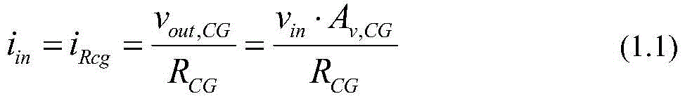
当电路满足输入匹配时,有Rin=RS,因此其输入阻抗Rin可以写为:When the circuit satisfies the input matching, there is R in = R S , so its input impedance R in can be written as:

可推出:Available:
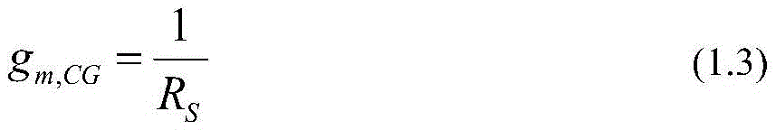

当M2满足下式时电路具有巴伦功能:The circuit has a balun function when M2 satisfies the following formula:

考虑由M1带来的噪声,将M1的热噪声等效为一个大小为Inoise的电流源,则噪声在节点IN引起的电压为:Considering the noise brought by M1, the thermal noise of M1 is equivalent to a current source whose size is I noise , then the voltage caused by the noise at the node IN is:
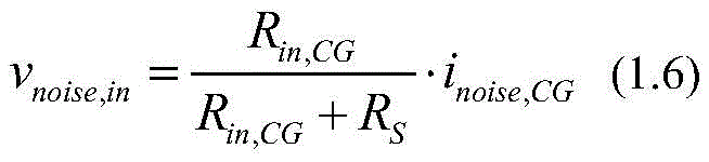
可得节点A、B中包含的噪声分别为:The noise contained in nodes A and B can be obtained as:
vnoise,CG=vnoise,in·AV,CG (1.7)v noise,CG = v noise,in · AV,CG (1.7)
vnoise,CS=vnoise,in·AV,CS=-vnoise,CG (1.8)v noise,CS =v noise,in · AV,CS =-v noise,CG (1.8)
由此可知电路消除了M1的热噪声。It can be seen that the circuit eliminates the thermal noise of M1.
考虑电路的非线性,M1的非线性漏源电流ids将对vin产生影响,又ids由电源电压vs决定,因此可以用vs表示vin:Considering the nonlinearity of the circuit, the nonlinear drain-source current i ds of M1 will affect v in , and i ds is determined by the power supply voltage v s , so v s can be used to represent v in :

其中α1表示一阶泰勒展开系数,vNL表示所有非线性项。则输出节点A、B的电压可以分别表示为:where α 1 represents the first-order Taylor expansion coefficient and v NL represents all nonlinear terms. Then the voltages of output nodes A and B can be expressed as:
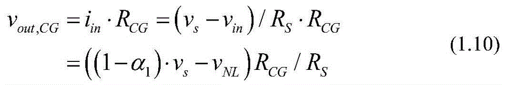
vout,CS=-vin·RCG/RS=-(α1·vs+vNL)·RCG/RS (1.11)v out, CS = -v in · R CG /R S = -(α 1 ·v s +v NL ) · R CG /R S (1.11)
电路差分输出为:The circuit differential output is:
vout,diff=vout,CG-vout,CS=vs·RCG/RS (1.12)v out,diff =v out,CG -v out,CS =v s ·R CG /R S (1.12)
上式中不包含非线性项,可见由M1导致的非线性在电路的差分输出端口抵消。The nonlinear term is not included in the above formula, and it can be seen that the nonlinearity caused by M1 is canceled at the differential output port of the circuit.
考虑到电路IF工作范围,在设计时需要额外考虑LNA的低频噪声。M2对电路噪声的贡献与其跨导gm,CS成反比,因此本发明对M2的跨导、面积与功耗进行了折衷。同时使用Poly电阻作为负载,进一步降低电路的1/f噪声。通过调节M1的参数使其跨导接近1/RS,同时在M1的栅极并联对地电容C以补偿输入信号的幅度与相位,能够使电路在5M~200M内获得良好的输入匹配。采用片上电阻R代替电流源为M2提供偏置,不仅能够节约芯片面积,而且有助于改善电路的匹配特性。Considering the circuit IF operating range, the low-frequency noise of the LNA needs to be additionally considered in the design. The contribution of M2 to circuit noise is inversely proportional to its transconductance g m,CS , so the present invention compromises the transconductance, area and power consumption of M2. At the same time, the Poly resistor is used as the load to further reduce the 1/f noise of the circuit. By adjusting the parameters of M1 to make its transconductance close to 1/R S , and at the same time connecting the capacitance C to ground in parallel with the gate of M1 to compensate the amplitude and phase of the input signal, the circuit can obtain good input matching within 5M~200M. Using the on-chip resistor R instead of the current source to provide bias for M2 not only saves chip area, but also helps to improve the matching characteristics of the circuit.
考虑到本振端口需要在更大的范围内实现宽带输入匹配,同时为了降低增益滚降对系统性能的影响,本振端口的低噪声放大器采用电阻电感串联结构作为负载,并在输入端添加电感进行匹配,其他结构与基带端口LNA结构相同。Considering that the local oscillator port needs to achieve broadband input matching in a wider range, and to reduce the impact of gain roll-off on system performance, the low-noise amplifier of the local oscillator port uses a resistor-inductor series structure as the load, and adds an inductor at the input end. For matching, other structures are the same as the baseband port LNA structure.
2.混频器2. Mixer
本发明采用的双平衡正交混频器电路结构如图4所示。The circuit structure of the double-balanced quadrature mixer adopted in the present invention is shown in FIG. 4 .
考察该电路输出节点A、B的电压:Consider the voltages at the output nodes A and B of this circuit:

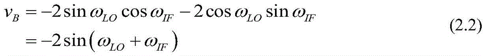
由此可见输出信号中仅包含和频成分,因此该结构免除了滤波器的使用。It can be seen that the output signal only contains sum-frequency components, so this structure eliminates the use of filters.
电路中跨导管M9~M12将输入IF电压信号转换为电流形式,开关管M1~M8由本振信号驱动工作于截止区与饱和区之间,对该电流进行开关调制,负载R1、R2将输出RF电流转换为电压信号,从而实现混频功能。同时在负载中串联电感L1、L2,目的是补偿高频增益衰减。Transductors M9-M12 in the circuit convert the input IF voltage signal into a current form. The switches M1-M8 are driven by the local oscillator signal to work between the cut-off region and the saturation region, and the current is switched and modulated. The loads R1 and R2 will output RF The current is converted into a voltage signal, thereby realizing the mixing function. At the same time, the inductors L1 and L2 are connected in series in the load to compensate the high frequency gain attenuation.
考虑到IF信号最低频率仅有5MHz,跨导级中的低频噪声经过频率转换后会对输出RF信号产生较大影响。该噪声幅度与输出RF频率和LO频率的差值成反比,主要来源为跨导级的1/f噪声。本发明通过增大跨导管面积,提高提高跨导管gm,适当增大LO信号摆幅来减小该噪声。开关级的噪声不经过任何频率转换直接输出,本发明通过减小开关级偏置电流,降低噪声脉冲的高度从而减小其噪声。Considering that the lowest frequency of the IF signal is only 5MHz, the low frequency noise in the transconductance stage will have a great impact on the output RF signal after frequency conversion. The magnitude of this noise is inversely proportional to the difference between the output RF frequency and the LO frequency, and the main source is the 1/f noise of the transconductance stage. The present invention reduces the noise by increasing the area across the conduit, increasing the g m across the conduit, and appropriately increasing the LO signal swing. The noise of the switching stage is directly output without any frequency conversion, and the present invention reduces the noise of the noise pulse by reducing the bias current of the switching stage and the height of the noise pulse.
该电路的非线性主要由跨导级决定,其三阶交调点表达式为:The nonlinearity of the circuit is mainly determined by the transconductance level, and its third-order intersection point is expressed as:

可以简化为:can be simplified to:
|IM3(2ω1-ω2)|∝|1+jωCgsZs(ω)| (2.4)|IM3(2ω 1 -ω 2 )|∝|1+jωC gs Z s (ω)| (2.4)
由于jωCgsZs(ω)项为负值,因此IM3的幅度与Zs和Cgs成反比。本设发明通过在跨导管栅源之间添加并联电感以提高晶体管原有Cgs,不以牺牲面积、增益或功耗为前提而增加线性度。Since the jωC gs Z s (ω) term is negative, the magnitude of IM3 is inversely proportional to Z s and C gs . The present invention is designed to increase the original C gs of the transistor by adding a parallel inductance between the gate-source across the conduit, without sacrificing area, gain or power consumption to increase linearity.
3.可变增益放大器3. Variable Gain Amplifier
为精确控制系统增益,同时降低带内增益起伏对输出信号功率的影响,本发明在Mixer与DA之间使用了一级具有20dB动态范围的可变增益放大器,电路结构如图5所示。In order to precisely control the system gain and reduce the influence of in-band gain fluctuations on the output signal power, the present invention uses a variable gain amplifier with a dynamic range of 20dB between the Mixer and the DA. The circuit structure is shown in Figure 5.
该VGA采用线性区工作的差分共源共栅结构。晶体管M1、M2能够起到提高增益、反向隔离度,以及减小晶体管M3、M4的密勒电容,改善稳定性等作用。The VGA uses a differential cascode structure that operates in the linear region. The transistors M1 and M2 can improve the gain and reverse isolation, reduce the Miller capacitance of the transistors M3 and M4, and improve the stability.
输入对管M3、M4工作在线性区,其等效跨导是漏源电压Vds3、Vds4的线性函数,可以写为:The input pair tubes M3 and M4 work in the linear region, and their equivalent transconductance is a linear function of the drain-source voltages V ds3 and V ds4 , which can be written as:
gm3=μ0COXW/L·Vds3 (3.1)g m3 = μ 0 C OX W/L·V ds3 (3.1)
M1、M2的跨导以及电路的电流可以表达为:The transconductance of M1, M2 and the current of the circuit can be expressed as:
gm1=μ0COXW/L·(Vgs1-Vth1)2 (3.2)g m1 = μ 0 C OX W/L·(V gs1 -V th1 ) 2 (3.2)
Ids1=μ0COXW/2L·(Vgs1-Vth1)2 (3.3)I ds1 = μ 0 C OX W/2L·(V gs1 -V th1 ) 2 (3.3)
Ids3=μ0COXW/L·[(Vgs3-Vth3)-Vds3/2]·Vds3 (3.4)I ds3 =μ 0 C OX W/L·[(V gs3 -V th3 )-V ds3 /2]·V ds3 (3.4)
联立式(3.3)和式(3.4),可以解出:Simultaneously formula (3.3) and formula (3.4) can be solved:

设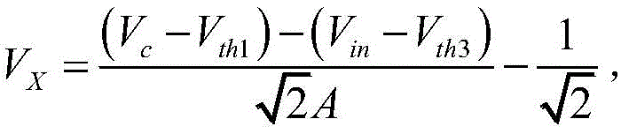

对上式进行泰勒展开变换,可以得到:The Taylor expansion transformation of the above formula can be obtained:
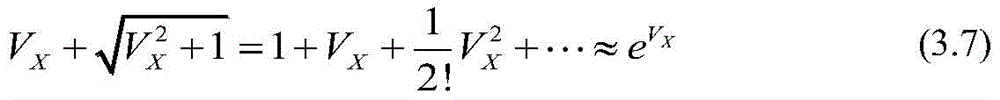
因此,在电路电流及负载保持恒定的情况下,通过对M3、M4栅电压的控制,可以使其跨导呈指数趋势变化,从而使VGA具有dB线性(Linear-in-dB)增益控制特性。Therefore, when the circuit current and load are kept constant, the transconductance can be changed exponentially by controlling the gate voltages of M3 and M4, so that the VGA has a linear-in-dB gain control characteristic.
4.驱动放大器4. Drive Amplifier
由于差分信号在系统中能够实现的噪声性能、隔离度及线性度等性能较单端信号具有明显优势,因此本发明在芯片内部使用差分信号,对于本级电路模块而言需要实现双端信号到单端信号的转换,同时还需对输出端口进行阻抗匹配设计。其电路拓扑结构如图6所示。Since the noise performance, isolation and linearity that the differential signal can achieve in the system has obvious advantages over the single-ended signal, the present invention uses the differential signal inside the chip, and for the circuit module of this stage, it is necessary to realize the double-ended signal to the The conversion of single-ended signals also requires impedance matching design for the output port. Its circuit topology is shown in Figure 6.
本发明采用共源放大器和源级跟随器来实现信号的双转单功能。晶体管M1作为源级跟随器,虽无电压增益,但其高输入阻抗、低输出阻抗使其拥有一定的功率增益。通过合理设计M1、M2的宽长比及偏置电压,利用源级跟随器对信号同相放大、共源放大器对信号进行反相放大的特点,实现信号的双转单功能。The invention adopts the common source amplifier and the source level follower to realize the double-to-single function of the signal. Transistor M1 acts as a source-level follower, although it has no voltage gain, but its high input impedance and low output impedance make it have a certain power gain. By rationally designing the width-length ratio and bias voltage of M1 and M2, and using the characteristics of the source-level follower to amplify the signal in-phase and the common-source amplifier to amplify the signal inversely, the double-to-single function of the signal is realized.
射频驱动放大器需要实现高输出功率,其线性度指标至关重要。本发明采用推挽放大器作为输出驱动放大器的结构,核心部分由上图中的晶体管M3(PMOS)、M4(NMOS)组成。M3和M4相反的工作状态,使得电路等效跨导、栅源电容等电路参数能够实现互补。通过对晶体管尺寸的设计,可使电路的g′m和g″m分别叠加抵消,从而消除跨导非线性。同时M3与M4的Cgs随输出电压变化方向相反,因而能够降低电路Cin的变化,减小AM-PM失真。RF driver amplifiers need to achieve high output power, and their linearity specifications are critical. The present invention adopts the push-pull amplifier as the structure of the output driver amplifier, and the core part is composed of the transistors M3 (PMOS) and M4 (NMOS) in the above figure. The opposite working states of M3 and M4 enable circuit parameters such as equivalent transconductance and gate-source capacitance to be complementary. Through the design of the transistor size, the g'm and g''m of the circuit can be superimposed and canceled respectively, thereby eliminating the transconductance nonlinearity. At the same time, the C gs of M3 and M4 change in opposite directions with the output voltage, so the circuit C in can be reduced. change to reduce AM-PM distortion.
考察该电路的输出阻抗,该输出阻抗的实部可以表达为:Considering the output impedance of this circuit, the real part of the output impedance can be expressed as:

因此通过合理设计电路偏置以及MOS管尺寸,可以实现电路良好的宽带阻抗匹配性能。电感L为匹配电路。Therefore, by reasonably designing the circuit bias and the size of the MOS tube, a good broadband impedance matching performance of the circuit can be achieved. Inductor L is a matching circuit.
本发明的具体结构如下:The concrete structure of the present invention is as follows:
其中基带LNA为:晶体管M1的栅极与电容C一端相连,源极与电阻R一端相连,漏极与电阻R1相连;晶体管M2的栅极与电阻R的一端相连,源极接地,漏极与电阻R2的一端连接;电容C另一端接地;电阻R另一端接地;电阻R1另一端接电源;电阻R2另一端接电源。The baseband LNA is: the gate of the transistor M1 is connected to one end of the capacitor C, the source is connected to one end of the resistor R, and the drain is connected to the resistor R1; the gate of the transistor M2 is connected to one end of the resistor R, the source is grounded, and the drain is connected to One end of the resistor R2 is connected; the other end of the capacitor C is grounded; the other end of the resistor R is connected to the ground; the other end of the resistor R1 is connected to the power supply; the other end of the resistor R2 is connected to the power supply.
其中本振LNA为:晶体管M1的栅极与电容C一端相连,源极与电阻R一端相连,漏极与电感L1相连,L1另一端与电阻R1相连;晶体管M2的栅极与电感L和电阻R的一端相连,源极接地,漏极与电感L2相连,L2另一端电阻R2的一端连接;电容C另一端接地;电阻R另一端接地;电阻R1另一端接电源;电阻R2另一端接电源。The local oscillator LNA is: the gate of the transistor M1 is connected to one end of the capacitor C, the source is connected to one end of the resistor R, the drain is connected to the inductor L1, and the other end of L1 is connected to the resistor R1; the gate of the transistor M2 is connected to the inductor L and the resistor. One end of R is connected, the source is grounded, the drain is connected to the inductor L2, and the other end of L2 is connected to one end of the resistor R2; the other end of the capacitor C is connected to the ground; the other end of the resistor R is connected to the ground; the other end of the resistor R1 is connected to the power supply; the other end of the resistor R2 is connected to the power supply .
其中混频器为:第一晶体管M1、第四晶体管M4的栅极连接反向本振I信号LO-I-,第二晶体管M2、第三晶体管M3的栅极连接正向本振I信号LO-I+,第五晶体管M5、第八晶体管M8的栅极连接反向本振I信号LO-I-,第六晶体管M6、第七晶体管M7的栅极连接正向本振I信号LO-I+。第一晶体管、第三晶体管、第五晶体管、第七晶体管的漏极与电阻R1的一端相连,R1的另一端与电感L1的一端相连,L1另一端接电源。第二晶体管、第四晶体管、第六晶体管、第八晶体管的漏极与电阻R2的一端相连,R2的另一端与电感L2的一端相连,L2另一端接电源。第一晶体管、第二晶体管的源极接第九晶体管M9的漏极。第三晶体管、第四晶体管的源极接第十晶体管M10的漏极。第五晶体管、第六晶体管的源极接第十一晶体管M11的漏极。第七晶体管、第八晶体管的源极接第十二晶体管M12的漏极。第九晶体管的栅极接正向中频信号QIF-Q+,源极接地。第十晶体管的栅极接反向中频信号Q(IF-Q-)。第十一晶体管的栅极接反向中频信号IIF-I-,源极接地。第十二晶体管的栅极接正向中频信号(IF-I+),源极接地。The mixer is: the gates of the first transistor M1 and the fourth transistor M4 are connected to the reverse local oscillator I signal LO-I-, and the gates of the second transistor M2 and the third transistor M3 are connected to the forward local oscillator I signal LO -I+, the gates of the fifth transistor M5 and the eighth transistor M8 are connected to the reverse local oscillator I signal LO-I-, and the gates of the sixth transistor M6 and the seventh transistor M7 are connected to the forward local oscillator I signal LO-I+. The drains of the first transistor, the third transistor, the fifth transistor and the seventh transistor are connected to one end of the resistor R1, the other end of R1 is connected to one end of the inductor L1, and the other end of L1 is connected to the power supply. The drains of the second transistor, the fourth transistor, the sixth transistor and the eighth transistor are connected to one end of the resistor R2, the other end of the R2 is connected to one end of the inductor L2, and the other end of the L2 is connected to the power supply. The sources of the first transistor and the second transistor are connected to the drain of the ninth transistor M9. The sources of the third transistor and the fourth transistor are connected to the drain of the tenth transistor M10. The sources of the fifth transistor and the sixth transistor are connected to the drain of the eleventh transistor M11. The sources of the seventh transistor and the eighth transistor are connected to the drain of the twelfth transistor M12. The gate of the ninth transistor is connected to the forward intermediate frequency signal QIF-Q+, and the source is connected to the ground. The gate of the tenth transistor is connected to the reverse intermediate frequency signal Q (IF-Q-). The gate of the eleventh transistor is connected to the reverse intermediate frequency signal IIF-I-, and the source is connected to the ground. The gate of the twelfth transistor is connected to the forward intermediate frequency signal (IF-I+), and the source is connected to the ground.
其中VGA为:第一晶体管M1的漏极接电阻R1的一端,R1另一端接电源;栅极接控制电压Vc;漏极接第三晶体管M3的漏极。第二晶体管M2的漏极接电阻R2的一端,R2另一端接电源;栅极接控制电压Vc;漏极接第四晶体管M4的漏极。第三晶体管的栅极接正向输入信号IN+,源极接电流源。第四晶体管的栅极接反向输入信号IN-,源极接电流源。The VGA is: the drain of the first transistor M1 is connected to one end of the resistor R1, the other end of R1 is connected to the power supply; the gate is connected to the control voltage Vc; the drain is connected to the drain of the third transistor M3. The drain of the second transistor M2 is connected to one end of the resistor R2, the other end of R2 is connected to the power supply; the gate is connected to the control voltage Vc; the drain is connected to the drain of the fourth transistor M4. The gate of the third transistor is connected to the forward input signal IN+, and the source is connected to the current source. The gate of the fourth transistor is connected to the reverse input signal IN-, and the source is connected to the current source.
其中驱动放大器模块为:第一晶体管M1的漏极接电源,栅极接正向输入信号IN+,源极接第二晶体管M2的漏极。第二晶体管的栅极接反向输入信号IN-,源极接地。第三晶体管M3的栅极通过电容连接到第一晶体管的源极,漏极接电源,源极接第四晶体管M4的漏极。第四晶体管的栅极通过电容连接到第二晶体管的漏极,漏极接电感L的一端,L另一端为输出,源极接地。The driving amplifier module is: the drain of the first transistor M1 is connected to the power supply, the gate is connected to the forward input signal IN+, and the source is connected to the drain of the second transistor M2. The gate of the second transistor is connected to the reverse input signal IN-, and the source is connected to the ground. The gate of the third transistor M3 is connected to the source of the first transistor through a capacitor, the drain is connected to the power supply, and the source is connected to the drain of the fourth transistor M4. The gate of the fourth transistor is connected to the drain of the second transistor through a capacitor, the drain is connected to one end of the inductor L, the other end of L is the output, and the source is grounded.
Claims (8)
Priority Applications (1)
| Application Number | Priority Date | Filing Date | Title |
|---|---|---|---|
| CN201710937103.4A CN107911092B (en) | 2017-10-10 | 2017-10-10 | A Broadband and High Linearity RF Transmitting Front-End Circuit |
Applications Claiming Priority (1)
| Application Number | Priority Date | Filing Date | Title |
|---|---|---|---|
| CN201710937103.4A CN107911092B (en) | 2017-10-10 | 2017-10-10 | A Broadband and High Linearity RF Transmitting Front-End Circuit |
Publications (2)
| Publication Number | Publication Date |
|---|---|
| CN107911092A CN107911092A (en) | 2018-04-13 |
| CN107911092B true CN107911092B (en) | 2020-11-27 |
Family
ID=61841222
Family Applications (1)
| Application Number | Title | Priority Date | Filing Date |
|---|---|---|---|
| CN201710937103.4A Expired - Fee Related CN107911092B (en) | 2017-10-10 | 2017-10-10 | A Broadband and High Linearity RF Transmitting Front-End Circuit |
Country Status (1)
| Country | Link |
|---|---|
| CN (1) | CN107911092B (en) |
Families Citing this family (19)
| Publication number | Priority date | Publication date | Assignee | Title |
|---|---|---|---|---|
| CN108957409A (en) * | 2018-07-12 | 2018-12-07 | 中国船舶重工集团公司第七二四研究所 | A kind of broadband transmitting-receiving subassembly improves the design method of anti-interference ability and miniaturization |
| CN108736847B (en) * | 2018-07-24 | 2023-09-01 | 成都嘉纳海威科技有限责任公司 | High-efficiency inverse D-type stacked power amplifier based on accurate resonant circuit control |
| CN109104160A (en) * | 2018-08-22 | 2018-12-28 | 广东工业大学 | A kind of radio-frequency power amplifier and wireless communication system |
| CN109743023B (en) * | 2018-12-24 | 2020-10-30 | 武汉大学 | A 24GHz Mixer with Up-down Conversion Multiplexing |
| EP3940953A4 (en) * | 2019-03-30 | 2022-03-09 | Huawei Technologies Co., Ltd. | VARIABLE GAIN AMPLIFIER AND PHASE CONTROLLED TRANSCEIVER |
| GB202007234D0 (en) * | 2020-05-15 | 2020-07-01 | Nordic Semiconductor Asa | Radio-frequency modulator apparatus |
| CN111600559B (en) * | 2020-06-16 | 2021-07-06 | 锐石创芯(深圳)科技有限公司 | Power amplifier output matching circuits, RF front-end modules and wireless devices |
| CN113098485B (en) * | 2021-04-02 | 2022-12-02 | 南方科技大学 | Double-rotation single-drive circuit |
| CN113437941B (en) * | 2021-06-11 | 2022-10-14 | 电子科技大学 | High-linearity single-sideband mixer with high-sideband suppression |
| CN113746431B (en) * | 2021-08-06 | 2024-01-05 | 天津大学 | An ultra-wideband and high linearity mixer with image suppression function |
| CN114046881B (en) * | 2021-11-15 | 2024-05-28 | 深圳知微创新技术有限公司 | High-sensitivity color sensor based on thin film transistor |
| CN114584076B (en) * | 2022-03-03 | 2024-04-16 | 北京大学 | A correction method for suppressing harmonics in a passive up-mixer of a transmitter |
| CN114598267B (en) * | 2022-04-12 | 2025-03-04 | 中国科学院空天信息创新研究院 | Bidirectional mixer |
| CN114785287B (en) * | 2022-06-17 | 2022-09-20 | 成都旋极星源信息技术有限公司 | Transmitter circuit and electronic equipment |
| CN114978074B (en) * | 2022-07-25 | 2022-11-11 | 成都嘉纳海威科技有限责任公司 | Three-channel transceiving amplification chip |
| CN115276573A (en) * | 2022-08-01 | 2022-11-01 | 浙江大学 | Phase temperature compensation amplifier integrated circuit based on transistor variable capacitor |
| CN117674816B (en) * | 2023-10-25 | 2024-09-20 | 隔空微电子(深圳)有限公司 | Co-local oscillator chip, cascade structure and working method |
| CN118018044B (en) * | 2024-04-09 | 2024-06-04 | 成都信息工程大学 | Ultra-wideband emission front-end system |
| CN119561558B (en) * | 2024-11-27 | 2025-07-08 | 广州润芯信息技术有限公司 | Front-end circuit of current type transmitter and transmitting system |
Family Cites Families (6)
| Publication number | Priority date | Publication date | Assignee | Title |
|---|---|---|---|---|
| CN102096079B (en) * | 2009-12-12 | 2013-12-11 | 杭州中科微电子有限公司 | Method for constructing radio frequency front end of multi-mode multi-band satellite navigation receiver and module thereof |
| US9300264B2 (en) * | 2014-08-22 | 2016-03-29 | Mediatek Inc. | Receiver arrangement and method of performing operations of receiver |
| CN105139049B (en) * | 2015-08-25 | 2018-02-27 | 华东师范大学 | Work in the 860~960MHz fully integrated UHF RFID readers radio frequency receiving front-end circuits of CMOS |
| CN105281802A (en) * | 2015-11-30 | 2016-01-27 | 武汉中元通信股份有限公司 | Broad-band radio frequency universal receiving/transmitting unit suitable for radio station |
| CN106385240B (en) * | 2016-11-30 | 2018-09-21 | 东南大学 | A kind of RF front-end circuit that gain is continuously adjustable |
| CN107134980B (en) * | 2017-06-14 | 2023-07-25 | 苏州大学 | RF single-ended to differential transconductance complementary high-performance down-mixer |
-
2017
- 2017-10-10 CN CN201710937103.4A patent/CN107911092B/en not_active Expired - Fee Related
Also Published As
| Publication number | Publication date |
|---|---|
| CN107911092A (en) | 2018-04-13 |
Similar Documents
| Publication | Publication Date | Title |
|---|---|---|
| CN107911092B (en) | A Broadband and High Linearity RF Transmitting Front-End Circuit | |
| CN107786168B (en) | High-gain high-isolation millimeter wave double-balanced passive subharmonic mixer | |
| CN101834567B (en) | Broadband gain adjustable low-noise amplifier | |
| CN103401508B (en) | A kind of low noise amplifier and frequency mixer emerging system | |
| CN101494441B (en) | Wideband low noise amplifier | |
| CN110635769B (en) | Differential low noise amplifier | |
| JP2012257290A (en) | Differential amplifier with active post-distortion linearization | |
| CN107645300A (en) | A kind of current multiplexing low-power consumption radio-frequency transmitter | |
| CN107070425A (en) | Broadband low-power consumption low-noise amplifier applied to wireless sensor network | |
| CN107196611A (en) | Broadband single-ended transfer difference low-noise amplifier | |
| CN111313844A (en) | An Adaptive Bias Circuit Applied to Low Noise Amplifier Chip | |
| CN107733375A (en) | Ultra-wideband low-noise amplifier | |
| CN104124923B (en) | A kind of low-noise mixer circuit | |
| CN111711424A (en) | A CMOS power amplifier and its radio frequency module | |
| CN114553147B (en) | Configurable Gain Double Balanced Passive Mixer | |
| CN103633947A (en) | Noninductive and high-gain CMOS (Complementary Metal Oxide Semiconductor) broadband low-noise amplifier | |
| US6980055B2 (en) | CMOS differential buffer circuit | |
| CN113904635A (en) | High-third-order intermodulation point field effect transistor radio frequency amplifier | |
| CN112910416A (en) | High-gain millimeter wave mixer applied to automobile radar | |
| CN117118466A (en) | A P-band frequency conversion transmission method and system | |
| WO2020000614A1 (en) | Frequency mixer circuit | |
| CN104104336B (en) | A kind of low-power consumption broadband rf front end circuit with noise cancellation | |
| CN106603013B (en) | Mixer circuit with complementary CMOS structure | |
| CN111478671A (en) | Novel low-noise amplifier applied to Sub-GHz frequency band | |
| CN114938206A (en) | Low-noise ultra-wideband active balun |
Legal Events
| Date | Code | Title | Description |
|---|---|---|---|
| PB01 | Publication | ||
| PB01 | Publication | ||
| SE01 | Entry into force of request for substantive examination | ||
| SE01 | Entry into force of request for substantive examination | ||
| GR01 | Patent grant | ||
| GR01 | Patent grant | ||
| CF01 | Termination of patent right due to non-payment of annual fee |
Granted publication date: 20201127 Termination date: 20211010 |
|
| CF01 | Termination of patent right due to non-payment of annual fee |