Disclosure of Invention
The embodiment of the invention aims to provide a method for processing data among multiple FPGA chips and a conversion device, which solve the problem of data transmission of the multiple FPGA chips in the process of verifying an ASIC chip in the prior art and realize the packaging and transmission of various interface signals.
In order to achieve the above object, an embodiment of the present invention provides a method for processing data between multiple FPGA chips, where the method is applied to a conversion device of an FPGA chip, and the conversion device is used for forwarding data between a data interface of the FPGA chip and a high-speed transceiver, and the method includes:
the steps of preparing the message to be sent are as follows:
storing the received signal data of the specific type according to a storage rule corresponding to the specific type;
in response to a transmission request for the stored signal data, the stored signal data is read out according to a fair round robin arbitration scheme and encapsulated in a message of a specified format for transmission of the message through the high speed transceiver.
Further, the storing the received signal data of the specific type according to the storage rule corresponding to the specific type includes: storing a specific type of signal data received from a flow-controlled data interface in a buffer with a first depth, wherein the specific type is a flow-controlled data type, the first depth is equal to an initial value of a credit value, and the credit value is maintained by the flow-controlled data interface.
Further, the reading out the stored signal data includes: when a signal data is read from the buffer of the first depth, 1 credit value is returned to the fluidic data interface.
Further, the storing the received signal data of the specific type according to the storage rule corresponding to the specific type includes: and storing the specific type of signal data received from the flow-free data interface in a buffer area with a second depth, wherein the specific type is a flow-free data type.
Further, the method further comprises: and sending out prompt information of signal data overflow when detecting that the storage space in the buffer with the second depth is full and receiving the signal data without flow control.
Further, the storing the received signal data of the specific type according to the storage rule corresponding to the specific type includes: when the signal data of which the specific type is the pulse signal type is received, 1 is added to the value in the designated counter.
Further, the storing the received signal data of the specific type according to the storage rule corresponding to the specific type includes: when signal data of which the specific type is a level signal type is received, the signal data is stored in a register.
Further, the message with the specified format includes a message type field, a sequence number field, a CRC field, and a data payload field, where the data payload field is used to carry signal data.
Further, the data payload field includes at least one specific type of signal data.
Further, the method further comprises:
splitting the message into micro packets with specified length so as to send the micro packets according to the splitting sequence of the micro packets through the high-speed transceiver, wherein the specified length is equal to the bit width of a parallel data interface of the high-speed transceiver, the micro packets comprise position fields and data fields, and the position fields are used for representing the positions of the micro packets in the message.
Further, the method further comprises:
the steps of processing the received message are as follows:
checking the received message according to a preset checking rule;
taking out the signal data carried in the message with correct verification;
and according to the specific type of the signal data, sending the signal data to a data interface corresponding to the specific type.
Further, before the received packet is verified according to the preset verification rule, the method further includes:
receiving a micro packet with a specified length, wherein the specified length is equal to the bit width of a parallel data interface of the high-speed transceiver, the micro packet comprises a position field and a data field, and the position field is used for representing the position of the micro packet in the message;
and assembling the micro packets into corresponding messages according to the receiving sequence according to the position fields.
Further, the packet includes a packet type field, a sequence number field, a CRC field, and a data payload field, where the data payload field is used to carry signal data.
Further, the verifying the received packet according to the preset verification rule includes: and checking the received message according to the sequence number field and the CRC field.
Further, the sending the signal data to a data interface corresponding to a specific type of the signal data according to the specific type includes: when the specific type of the signal data is a data type with flow control, storing the signal data in a buffer area corresponding to a first depth in a data interface with flow control, and subtracting 1 from a local credit value, wherein the first depth is equal to an initial value of the credit value.
Further, the method further comprises: and when the flow-controlled data interface reads out a signal data from the buffer with the first depth, receiving 1 credit value returned by the flow-controlled data interface.
Further, the sending the signal data to a data interface corresponding to a specific type of the signal data according to the specific type includes: and when the specific type of the signal data is a data type without flow control, sending the signal data to a corresponding data interface without flow control.
Further, the sending the signal data to a data interface corresponding to a specific type of the signal data according to the specific type includes:
when the specific type of the signal data is a pulse signal type, the signal data is stored in a designated counter,
wherein the designated counter is decremented by 1 when a signal data is transmitted to the pulse signal interface.
Further, the sending the signal data to a data interface corresponding to a specific type of the signal data according to the specific type includes:
when the specific type of the signal data is a level signal type, storing the signal data in a register;
and sending the signal data in the register to a level signal interface.
The embodiment of the present invention further provides a conversion device, which is applied between a data interface of an FPGA chip and a high-speed transceiver to forward data, and the conversion device includes:
the storage unit is used for storing the received signal data of the specific type according to a storage rule corresponding to the specific type;
and the packaging unit is used for responding to a sending request aiming at the stored signal data, reading the stored signal data according to a fair round robin arbitration mechanism, and packaging the stored signal data into a message with a specified format so as to send the message through the high-speed transceiver.
Further, the storage unit is further configured to store a specific type of signal data received from the flow-controlled data interface in a buffer at a first depth, where the specific type is a flow-controlled data type, the first depth is equal to an initial value of a credit value, and the credit value is maintained by the flow-controlled data interface.
Further, the encapsulation unit includes: and the processing module is used for returning 1 credit value to the data interface with the flow control when a signal datum is read out from the buffer with the first depth.
Further, the storage unit is further configured to store a specific type of signal data received from the fluidionless data interface in a buffer at the second depth, where the specific type is a fluidionless data type.
Further, the apparatus further comprises: and the prompting unit is used for sending out the prompt information of signal data overflow when the storage space in the buffer with the second depth is detected to be full and the signal data without flow control is received.
Further, the storage unit is further configured to add 1 to the value in the designated counter when the signal data of which the specific type is the pulse signal type is received.
Further, the storage unit is further configured to store the signal data in a register when the signal data of which the specific type is a level signal type is received.
Further, the message in the specified format encapsulated by the encapsulation unit includes a message type field, a sequence number field, a CRC field, and a data payload field, where the data payload field is used to carry signal data.
Further, the data payload field in the message of the specified format encapsulated by the encapsulation unit includes at least one specific type of signal data.
Further, the apparatus further comprises:
the splitting unit is configured to split the packet into a micro packet with a specified length, so that the micro packet is sent by the high-speed transceiver according to a splitting order of the micro packet, where the specified length is equal to a bit width of a parallel data interface of the high-speed transceiver, the micro packet includes a position field and a data field, and the position field is used to indicate a position of the micro packet in the packet.
Further, the apparatus further comprises:
the verification unit is used for verifying the received message according to a preset verification rule;
the processing unit is used for taking out the signal data carried in the message with correct verification;
and the sending unit is used for sending the signal data to a data interface corresponding to the specific type according to the specific type of the signal data.
Further, the apparatus further comprises:
a receiving unit, configured to receive a micro packet with a specified length, where the specified length is equal to a bit width of a parallel data interface of the high-speed transceiver, and the micro packet includes a location field and a data field, where the location field is used to indicate a location of the micro packet in the message;
and the assembling unit is used for assembling the micro packets into corresponding messages according to the receiving sequence according to the position fields.
Further, the received message includes a message type field, a sequence number field, a CRC field, and a data payload field, where the data payload field is used to carry signal data.
Further, the checking unit is further configured to check the received packet according to the sequence number field and the CRC field.
Further, the sending unit is further configured to, when the specific type of the signal data is a data type with flow control, store the signal data in a buffer corresponding to a first depth in a data interface with flow control, and subtract 1 from a local credit value, where the first depth is equal to an initial value of the credit value.
Further, the apparatus further comprises: and the credit value receiving unit is used for receiving 1 credit value returned by the flow control data interface when the flow control data interface reads out one signal data from the buffer with the first depth.
Further, the sending unit is further configured to send the signal data to a corresponding flow-free data interface when the specific type of the signal data is a flow-free data type.
Further, the transmission unit includes:
the first storage module is used for storing the signal data in a specified counter when the specific type of the signal data is a pulse signal type;
and the processing module is used for subtracting 1 from the designated counter when sending a signal data to the pulse signal interface.
Further, the transmission unit includes:
the second storage module is used for storing the signal data in a register when the specific type of the signal data is a level signal type;
and the sending module is used for sending the signal data in the register to a level signal interface.
The received signal data of a specific type is stored according to a storage rule corresponding to the specific type by a conversion device arranged between an FPGA chip and a high-speed transceiver, the stored signal data is read out according to a fair rotation arbitration mechanism in response to a sending request aiming at the stored signal data, and is packaged in a message of a specified format, and the message is sent by the high-speed transceiver. The embodiment of the invention solves the problem of data transmission of a plurality of FPGA chips in the process of verifying the ASIC chip in the prior art, and realizes the packaging and transmission of various interface signals.
Additional features and advantages of embodiments of the invention will be set forth in the detailed description which follows.
Detailed Description
The following detailed description of embodiments of the invention refers to the accompanying drawings. It should be understood that the detailed description and specific examples, while indicating embodiments of the invention, are given by way of illustration and explanation only, not limitation.
When a large ASIC chip is logically divided, it is necessary to cut between main functional components according to the direction of data flow. Therefore, signal interfaces between the cut modules are simple, and data transmission across the FPGA chip is easy to carry out. Generally, the data interface is classified into the following types:
(1) data interface with flow control
In ASIC chip design, the data interface between two modules, if having flow control function, generally adopts a flow control mechanism based on credit value. Under the flow control mechanism, a sending credit counter is maintained at a sending party, a receiving data buffer area is maintained at a receiving party, and the initial value of the sending party credit counter is equal to the maximum depth of the receiving party data buffer area. When the sender gives a data to the receiver, a credit value of the sender is consumed; the data enters a data buffer area of a receiver and occupies one of the storage units; if the receiver needs to process the data in the buffer, taking out one data from the buffer for processing, and returning a credit value to the sender; the sender, upon receiving the credit returned from the receiver, supplements it to a credit counter.
(2) Non-flow control data interface
This kind of non-flow control data interface does not need flow control of data between the sender and the receiver, which means the following 3 different meanings: the sender generates data slower and has the ability to process it at the receiver; having a buffer at the receiver large enough to receive data from the sender without loss; the transmitted data is not lost even if the receiving party is not in time to process the data, and normal logic processing cannot be influenced.
(3) Pulse signal interface with fast change rate
This type of signal data is valid if it is 1 in a certain clock cycle; if 0 in a certain clock cycle, it is invalid. When such signal data is transmitted from one FPGA chip to another FPGA chip, how many clock cycles a sender has is 1, and the same number of cycles is required to be 1 at a receiver. In the worst case, the transmitting side may continuously transmit this type of signal data for a long time, but the receiving side may not have time to process the signal data because other processes are simultaneously performed. Therefore, a receiving buffer with a certain capacity needs to be maintained at the receiving end to temporarily store the signal data transmitted from the transmitting end.
In addition, this type of signal data is generally not continuously transmitted. After a plurality of signal data are continuously transmitted, the transmission is stopped for a certain period of time. For example, the credit return signal data mentioned above is of this type.
(4) Level signal interface with slow change rate
Signal data of this level signal type generally remains for a long time after the value changes from 0 to 1 or from 1 to 0 before the next state change occurs. It is simply a status signal indicating that the current system is in a certain state, which is often seen in some interrupts or error status signals. For this type of signal data, only the information of the state change needs to be transmitted to the other end, and there is no time requirement.
There may be a plurality of sets of signal data for each of the above 4 types of signal data. The embodiment of the invention aims at the 4 types of signal data to be transmitted among the multiple FPGA chips.
In addition, a plurality of high-speed transceivers are generally provided in a currently common middle-high-end FPGA chip, and provide a set of parallel interfaces for signal data, perform parallel-to-serial conversion inside the high-speed transceivers, and provide a set of high-speed serial differential signals outside the FPGA chip. The two FPGA chips are connected through a high-speed serial signal, and parallel data are transmitted between the two chips. According to the difference of chips, PCB processing technology and plates, the data transmission rate of the high-speed transceiver to differential signals can be different from 1Gbps to 10Gbps, and some high-grade chips even can reach 20Gbps to 30 Gbps. Moreover, in order to increase the total transmission bandwidth, multiple high-speed transceivers are often bundled together (each transceiver and its differential signal transmission link are referred to as 1 lane), and a serial-to-parallel conversion interface with multiple lane bindings is formed.
In order to quickly transmit the various signal data from one FPGA chip to another FPGA chip through the high-speed serial interface, in the embodiment of the present invention, a conversion device is respectively designed on the FPGA chips at the two ends for performing data forwarding between the data interface in the FPGA chip and the high-speed transceiver.
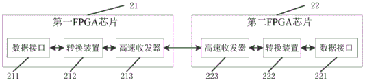
Fig. 1 is a flowchart of a method for processing data between multiple FPGA chips according to an embodiment of the present invention. The method is applied to the conversion device 212 between the data interface 211 of the first FPGA chip 21 and the high-speed transceiver 213 shown in fig. 2, and as shown in fig. 1, the method includes the following steps of preparing a message to be sent:
101. and storing the received signal data of the specific type according to a storage rule corresponding to the specific type.
Wherein the specific types include the types in 4 mentioned above: a data type with flow control, a data type without flow control, a pulse signal type and a level signal type.
And after receiving the signal data of each specific type from each data interface, the conversion device at the local end stores the signal data according to the storage rule corresponding to the specific type.
102. In response to a transmission request for the stored signal data, the stored signal data is read out according to a fair round robin arbitration scheme and encapsulated in a message of a specified format for transmission of the message through the high speed transceiver.
After each specific type of signal data is stored, a transmission request is issued in real time, and a fair round robin arbitration mechanism is adopted among the specific types of signal data. All the signal data of specific types have the same priority in the fair round robin arbitration mechanism, and the signal data of specific types are allowed to be sent out in turn. A specific type of signal data is selected by a fair round robin arbitration mechanism to be read out and packaged in a message with a specified format.
The message with the specified format includes a message type field, a sequence number field, a Cyclic Redundancy Check (CRC) field, and a data payload field, where the data payload field is used to carry signal data. For example, as shown in fig. 3, the message with the specified format may include a 2-bit type field, a 10-bit sequence number field, a 32-bit CRC field, and an n-bit data payload field, and the total length of the message is n +44 bits.
The message type field identifies the type of the message, and the bit number of the field is not limited, and may be 2 bits, 3 bits or more, and is related to the message specifically set by the user. For the sequence number field, the sequence number field of the first message is 0, then every time a message is generated, the field is added with 1, if the sequence number field is changed to all 1, the sequence number field of the next message is changed to 0, thereby distinguishing the sending sequence of the message. The CRC field is used to check the correctness of data transmission, and generally a 32-bit CRC field is used, and in some special cases, for example, in the case of a short message length, a 16-bit or 8-bit CRC field may be used, and when the message length is longer, in order to improve the checking efficiency, 2 32 CRC fields may be used to check, so that the number of bits of the CRC field is not limited, and is specifically related to the length of the message.
The received signal data of a specific type is stored according to a storage rule corresponding to the specific type by a conversion device arranged between an FPGA chip and a high-speed transceiver, the stored signal data is read out according to a fair rotation arbitration mechanism in response to a sending request aiming at the stored signal data, and is packaged in a message of a specified format, and the message is sent by the high-speed transceiver. The embodiment of the invention solves the problem of data transmission of a plurality of FPGA chips in the process of verifying the ASIC chip in the prior art, and realizes the packaging and transmission of various interface signals.
According to an embodiment of the present invention, since the bit width of the parallel data interface of the high-speed transceiver is fixed, when a packet is too long, 1 packet may be split into a micro packet with a specified length, so that the micro packet is sent by the high-speed transceiver according to the splitting order of the micro packet, where the specified length is equal to the bit width of the parallel data interface of the high-speed transceiver, the micro packet includes a position field and a data field, the position field is used to indicate the position of the micro packet in the packet, and the data field is used to carry data in the split packet. The position field includes a header flag bit (H) and a tail flag bit (T), and when H is 1 and T is 0, the position field indicates that the packet is the first packet in the entire message, when H is 0 and T is 1, the position field indicates that the packet is the last packet in the entire message, when H is 0 and T is 0, the position field indicates that the packet is the middle packet in the entire message, and when H is 1 and T is 1, the position field indicates that the message only includes one packet. As shown in fig. 4, a format of a micro packet is given by taking a micro packet with a length of 64 bits as an example, wherein the first two bits are a position field, and the last 62 bits are a data field.
In addition, when the micro packets are sent, the micro packets are sent according to the splitting sequence, and the sequence of the micro packets when the micro packets are reassembled into the message cannot be disturbed.
For the step 101 in the above embodiment, different specific types of signal data are stored by using different storage rules, which are described below for the specific types of signal data in fig. 4:
(1) for data types with flow control
Storing a specific type of signal data received from a flow-controlled data interface in a buffer with a first depth, wherein the specific type is a flow-controlled data type, the first depth is equal to an initial value of a credit value, and the credit value is maintained by the flow-controlled data interface.
Similar to the flow control mechanism based on credit value adopted by the flow-controlled data interface in the prior art, after the flow-controlled data interface sends a signal data to the conversion device, the signal data is stored in the buffer with the first depth, and a credit value of the flow-controlled data interface is consumed, when all the credit values are consumed, the credit data can not be sent to the conversion device any more.
When a signal data is read from the buffer of the first depth, 1 credit value is returned to the fluidic data interface. That is, when the signal data stored in the buffer of the first depth is read, it indicates that there is a storage space in the buffer of the first depth, several signal data are read, that is, several credit values are returned to the data interface with the flow control, and after there is a credit value in the data interface with the flow control, the signal data can be sent to the conversion device.
(2) For non-flow control data types
And storing the specific type of signal data received from the flow-free data interface in a buffer area with a second depth, wherein the specific type is a flow-free data type. For the non-flow control data type, the depth of the buffer with the second depth is set to be as large as possible, for example, the second depth is 1024, so that signal data sent by the non-flow control data interface is prevented from being buffered and not lost.
In addition, in order to avoid that in some cases, the signal data sent by the non-flow control data interface is lost and cannot be perceived due to the insufficient depth of the buffer with the second depth, when it is detected that the storage space in the buffer with the second depth is full and the non-flow control signal data is received, a prompt message of signal data overflow is sent out so as to notify a user that the data loss is caused by the data overflow on the non-flow control data interface.
(3) For pulse signal type
When the signal data of which the specific type is the pulse signal type is received, 1 is added to the value in the designated counter. For example, when the signal is 1 in a certain clock cycle, the value in the designated counter is increased by 1. And after passing through a fair rotation arbitration mechanism, when the signal data of the pulse signal type is transmitted in turn, packaging the value in the designated counter in a message and transmitting the message.
(4) For level signal type
When signal data of which the specific type is a level signal type is received, the signal data is stored in a register. For the signal data of the type, only the value of the signal data needs to be recorded in a register, and after passing through a fair round robin arbitration mechanism, the signal data of the level signal type is packaged in a message and sent.
In another embodiment of the present invention, in order to improve the utilization rate of the packet, the data payload field of the packet includes at least one specific type of signal data, that is, two specific types of signal data may share one packet for transmission. As shown in fig. 5, the signal data transmission between the egr module in one FPGA chip and the dic module in another FPGA chip is taken as an example for explanation, wherein the data types of the current control are egr _ dic _ vld, egr _ dic _ data and dic _ egr _ release, and dic _ egr _ vld, dic _ egr _ data and egr _ dic _ release; the non-flow control data types are 3 groups of signal data csr _ chain0_, csr _ chain1 _andcsr _ chain2 _; int is one-way interrupt signal data, which belongs to signal data of a level signal type with a slow change rate; copy done and release belong to the signal data of the pulse signal type having a fast rate of change. In the embodiment, the high-speed serial transceiver uses a 4lane binding mode, each lane provides 5Gbps bandwidth, and the 4 lanes have 20Gbps data transmission bandwidth in total. The high-speed transceiver provides a 64-bit parallel data interface to the outside.
And respectively defining respective message formats aiming at the specific types of signal data. For the signal data of egr _ dic _ vld and egr _ dic _ data, the defined message format is as shown in fig. 6. The data bit width is very wide, single CRC check efficiency is low, so that 2 CRC fields with 32 bits are adopted to check the whole message in a segmented mode, in addition, a sequence number field with 20 bits is adopted, a release _ info field with 136 bits is used for transmitting a copy _ done field, each copy _ done is stored by 1 counter with 4 bits, 15 count values can be transmitted each time, and therefore copy _ done signals transmitted in the loading mode can transmit 34 counters at most each time. The 4-bit release _ cnt field is used to transmit a credit release signal in the reverse direction. The message is additionally provided with a 3-bit Type field for indicating which Type of message the message currently belongs to, and the Type value of the current message is 001. Thus, the entire message has a width of 2054 bits and needs to be divided into 34 micro packets, each of which has a width of 64 bits and includes a position field of 2 bits and a data field of 62 bits.
For the signal data of dic _ egr _ vld and dic _ egr _ data, the defined message format is as shown in fig. 7. The whole message width is 1751 bits and needs to be divided into 29 micro packets. For the current message, the type value is 010. The meaning of each field thereof is similar to the signal data of the egr _ dic _ vld and egr _ dic _ data described earlier. The method comprises the steps of adopting 2 32-bit CRC fields to check the whole message in a segmented mode, adopting a 20-bit sequence number field, adopting a 136-bit release _ info field for transmitting a copy _ done field, storing each copy _ done by using 1 4-bit counter, and transmitting 15 count values each time, so that the copy _ done signal transmitted in the piggyback mode can transmit the count values of 34 counters at most each time. The 4-bit release _ cnt field is used to transmit a credit release signal in the reverse direction.
For 3 sets of data type of csr signal data without flow control, each set of data is 87 bits wide, and therefore the message format is as shown in fig. 8. Because the data width is very small, an 8-bit CRC check algorithm is adopted, and the 20-bit sequence number is still used for message sequence check. The 3-bit Type field is used for distinguishing specific message types, and the Type values of the csr signal data of the 3 groups of flow-control-free data types are 011, 100 and 101 respectively.
For the 2-bit interrupt signal int, that is, the signal data of the level signal type, a message format may be organized, as shown in fig. 9, which includes not only the 2-bit interrupt status signal, but also the credit value (release _ cnt) that needs to be reversely released, and the copy _ done and release signals of 34 bits, and it is intended that when no data message passes through and no piggyback transmission is possible, the credit value release signal and the copy _ done and release signals that the user needs may be transmitted through a specific message, so as to improve the utilization rate of the message.
The received signal data of a specific type is stored according to a storage rule corresponding to the specific type by a conversion device arranged between an FPGA chip and a high-speed transceiver, the stored signal data is read out according to a fair rotation arbitration mechanism in response to a sending request aiming at the stored signal data, and then the stored signal data is packaged in a message of a specified format, and the message is sent by the high-speed transceiver. The embodiment of the invention solves the data transmission problem of a plurality of FPGA chips in the verification process of the ASIC chip in the prior art, realizes the encapsulation and transmission of various interface signals, and can carry other types of signal data by utilizing the available space of the message, thereby fully improving the transmission efficiency of the message.
In another embodiment of the present invention, the first FPGA chip may also be used as a receiving party to process the received message, as shown in fig. 10, the method further includes the following steps of processing the received message:
1001. and checking the received message according to a preset checking rule.
The received message comprises a message type field, a sequence number field, a CRC field and a data load field, wherein the data load field is used for carrying signal data.
The message type field identifies the type of the message, and the bit number of the field is not limited, and may be 2 bits, 3 bits or more, and is related to the message specifically set by the user. For the sequence number field, the sequence number field of the first message is 0, then every time a message is generated, the field is added with 1, if the sequence number field is changed to all 1, the sequence number field of the next message is changed to 0, thereby distinguishing the sending sequence of the message. The CRC field is used to check the correctness of data transmission, and generally a 32-bit CRC field is used, and in some special cases, for example, in the case of a short message length, a 16-bit or 8-bit CRC field may be used, and when the message length is longer, in order to improve the checking efficiency, 2 32 CRC fields may be used to check, so that the number of bits of the CRC field is not limited, and is specifically related to the length of the message.
And checking the received message according to the sequence number field and the CRC field. Reference may be made to the prior art for checking messages by means of CRC. In addition, the embodiment of the invention can also check the message by using the sequence number field in the message. Since the sequence number field of the first packet is 0 in the sequence number field, after each packet is generated, the sequence number field is added with 1, and if the sequence number field becomes all 1, the sequence number field of the next packet becomes 0 again. If the sequence number field is checked to be in error, it indicates that 1 or more messages are lost in the transmission process. The CRC field can check whether the packet is erroneous during transmission through the high-speed link, and if the packet is erroneous, it indicates that some micro packets of the packet are erroneous or lost during transmission through the link, so as to notify the user. Through the two error detection mechanisms, most errors which can occur when a plurality of messages are transmitted through a high-speed link can be detected.
In an embodiment of the present invention, since a bit width of a parallel data interface of the high-speed transceiver is fixed, when a packet is too long, an opposite end may split 1 packet into micro packets with a specified length, where the specified length is equal to a bit width of the parallel data interface of the high-speed transceiver, and then a local end receives the micro packets with the specified length before checking the received packet according to a preset checking rule, where the micro packets include a position field and a data field, and the position field is used to indicate a position of the micro packet in the packet, and then assembles the micro packets into corresponding packets according to a receiving sequence according to the position field.
The position field includes a header flag bit (H) and a tail flag bit (T), and when H is 1 and T is 0, the position field indicates that the packet is the first packet in the entire message, when H is 0 and T is 1, the position field indicates that the packet is the last packet in the entire message, when H is 0 and T is 0, the position field indicates that the packet is the middle packet in the entire message, and when H is 1 and T is 1, the position field indicates that the message only includes one packet. Then after receiving multiple micro packets, according to H and T in the location field, the first and last micro packets of the message can be known, so as to assemble the corresponding message together with the middle micro packets. When the position field is H ═ 1 and T ═ 0, it is indicated that the micro packet is the first micro packet of another packet, so that the micro packets of the respective packets can be distinguished.
1002. Taking out the signal data carried in the message with correct verification;
1003. and according to the specific type of the signal data, sending the signal data to a data interface corresponding to the specific type.
And taking out the signal data carried in the message which is correctly checked, and sending the signal data to a data interface corresponding to the specific type according to the specific type of the signal data.
For the step 1003 in the above embodiment, different processing methods are adopted for different specific types of signal data, and the following is respectively described for specific types of signal data in 4:
(1) for data types with flow control
When the specific type of the signal data is a data type with flow control, storing the signal data in a buffer area corresponding to a first depth in a data interface with flow control, and subtracting 1 from a local credit value, wherein the first depth is equal to an initial value of the credit value.
When the flow-controlled data interface reads out a signal data from the buffer with the first depth, 1 credit value returned by the flow-controlled data interface is received, and then 1 is added to the local credit value.
(2) For non-flow control data types
And when the specific type of the signal data is a data type without flow control, sending the signal data to a corresponding data interface without flow control.
(3) For pulse signal type
And when the specific type of the signal data is a pulse signal type, storing the signal data in a designated counter, wherein when one signal data is sent to the pulse signal interface, the designated counter is reduced by 1. In addition, each time signal data of this type is received, the value of the signal data is added to the specified counter.
(4) For level signal type
And when the specific type of the signal data is a level signal type, storing the signal data in a register, and sending the signal data in the register to a level signal interface.
It should be noted that there may be multiple sets of each of the above 4 types of signal data. For signal data of type 1 and type 2, if there are multiple groups, each group of signal data has respective buffer area; for signal data of type 3 and type 4, if there are multiple groups of signals, the multiple groups of signals may be merged and organized into one message, and share the same set of check field, message encapsulation and parsing processing logic.
In addition, in an actual ASIC chip, data transmission between two adjacent modules tends to be bidirectional. At each end there is a transmitting device and a receiving device. Since the high-speed transceivers are bi-directional in nature, the bi-directional data transmission will share a set of high-speed transceivers to realize bi-directional data transmission, as shown in fig. 2. Meanwhile, data transmission is carried out in both directions, so that a credit carrying mode can be adopted for reverse credit value transmission, and the released credit value is transmitted back to the transmitting end by using a certain section of idle field in the message while the reverse data transmission is carried out. This will improve the transmission efficiency of network messages to some extent.
For signal data of a data type with flow control, in the original ASIC design, when data is read from a buffer of a receiving end, a credit value is directly returned to a credit management module of the transmitting end. At present, a sending end and a receiving end are divided into 2 different chips, and long conversion logic is arranged between the sending end and the receiving end, so that the original credit flow control needs to be divided into a plurality of sections for respective processing. Specifically, there is credit flow control processing between the data interface and the conversion device of the sender, between the conversion device of the sender and the conversion device of the receiver, and between the conversion device of the receiver and the data interface. Thus, a reverse credit return path is also required between the converting means of the transmitting side and the converting means of the receiving side for transmitting the reverse credit to the transmitting side. For this reason, it is also necessary to count the credit value, CRC check and encapsulate it into a message, which is similar to the process of pulse signal type message processing. For example, the message formats in fig. 6, 7 and 9 include a reverse credit release _ cnt signal.
Correspondingly, fig. 11 is a schematic structural diagram of a conversion device according to an embodiment of the present invention. The conversion device is applied to forward data between the data interface 211 of the first FPGA chip 21 shown in fig. 2 and the high-speed transceiver 213, and as shown in fig. 11, the conversion device 212 includes:
a storage unit 1101 configured to store the received signal data of a specific type according to a storage rule corresponding to the specific type;
a packaging unit 1102, configured to, in response to a transmission request for the stored signal data, read out the stored signal data according to a fair round robin arbitration mechanism and package the read out signal data into a message in a specified format, so as to transmit the message through the high-speed transceiver.
The received signal data of a specific type is stored according to a storage rule corresponding to the specific type by a conversion device arranged between an FPGA chip and a high-speed transceiver, the stored signal data is read out according to a fair rotation arbitration mechanism in response to a sending request aiming at the stored signal data, and is packaged in a message of a specified format, and the message is sent by the high-speed transceiver. The embodiment of the invention solves the problem of data transmission of a plurality of FPGA chips in the process of verifying the ASIC chip in the prior art, and realizes the packaging and transmission of various interface signals.
Further, the storage unit is further configured to store a specific type of signal data received from the flow-controlled data interface in a buffer at a first depth, where the specific type is a flow-controlled data type, the first depth is equal to an initial value of a credit value, and the credit value is maintained by the flow-controlled data interface.
Further, as shown in fig. 12, the encapsulation unit includes:
a processing module 1201, configured to return 1 credit value to the fluidic data interface when a signal data is read out from the buffer with the first depth.
Further, the storage unit is further configured to store a specific type of signal data received from the fluidionless data interface in a buffer at the second depth, where the specific type is a fluidionless data type.
Further, as shown in fig. 13, the apparatus further includes:
and a prompt unit 1301, configured to send a prompt message of signal data overflow when it is detected that the storage space in the buffer at the second depth is full and no-flow control signal data is received.
Further, the storage unit is further configured to add 1 to the value in the designated counter when the signal data of which the specific type is the pulse signal type is received.
Further, the storage unit is further configured to store the signal data in a register when the signal data of which the specific type is a level signal type is received.
Further, the message in the specified format encapsulated by the encapsulation unit includes a message type field, a sequence number field, a CRC field, and a data payload field, where the data payload field is used to carry signal data.
Further, the data payload field in the message of the specified format encapsulated by the encapsulation unit includes at least one specific type of signal data.
Further, as shown in fig. 14, the apparatus further includes:
a splitting unit 1401, configured to split the packet into a micro packet with a specified length, so as to send the micro packet through the high-speed transceiver according to a splitting order of the micro packet, where the specified length is equal to a bit width of a parallel data interface of the high-speed transceiver, and the micro packet includes a position field and a data field, where the position field is used to indicate a position of the micro packet in the packet.
Further, as shown in fig. 15, the conversion apparatus further includes:
the verification unit 1501 is configured to verify the received message according to a preset verification rule;
a processing unit 1502, configured to take out signal data carried in a correctly verified message;
a sending unit 1503, configured to send the signal data to a data interface corresponding to the specific type according to the specific type of the signal data.
Further, as shown in fig. 16, the apparatus further includes:
a receiving unit 1601, configured to receive a micro packet with a specified length, where the specified length is equal to a bit width of a parallel data interface of the high-speed transceiver, and the micro packet includes a location field and a data field, where the location field is used to indicate a location of the micro packet in the message;
an assembling unit 1602, configured to assemble the micro packets into corresponding packets according to the receiving order according to the location field.
Further, the received message includes a message type field, a sequence number field, a CRC field, and a data payload field, where the data payload field is used to carry signal data.
Further, the checking unit is further configured to check the received packet according to the sequence number field and the CRC field.
Further, the sending unit is further configured to, when the specific type of the signal data is a data type with flow control, store the signal data in a buffer corresponding to a first depth in a data interface with flow control, and subtract 1 from a local credit value, where the first depth is equal to an initial value of the credit value.
Further, as shown in fig. 17, the apparatus further includes:
a credit receiving unit 1701, configured to receive 1 credit returned by the flow-controlled data interface when the flow-controlled data interface reads out one signal data from the buffer with the first depth.
Further, the sending unit is further configured to send the signal data to a corresponding flow-free data interface when the specific type of the signal data is a flow-free data type.
Further, as shown in fig. 18, the transmitting unit includes:
a first storage module 1801, configured to store the signal data in a designated counter when the specific type of the signal data is a pulse signal type;
a processing module 1802 for decrementing the assigned counter by 1 when sending a signal data to the pulse signal interface.
Further, as shown in fig. 19, the transmitting unit includes:
a second storage module 1901, configured to store the signal data in a register when the specific type of the signal data is a level signal type;
a sending module 1902, configured to send the signal data in the register to a level signal interface.
The specific implementation process of each unit in the conversion device 212 may participate in the processing process of the above-mentioned method for processing data between multiple FPGA chips.
Although the embodiments of the present invention have been described in detail with reference to the accompanying drawings, the embodiments of the present invention are not limited to the details of the above embodiments, and various simple modifications can be made to the technical solutions of the embodiments of the present invention within the technical idea of the embodiments of the present invention, and the simple modifications all belong to the protection scope of the embodiments of the present invention.
It should be noted that the various features described in the above embodiments may be combined in any suitable manner without departing from the scope of the invention. In order to avoid unnecessary repetition, the embodiments of the present invention do not describe every possible combination.
Those skilled in the art will understand that all or part of the steps in the method according to the above embodiments may be implemented by a program, which is stored in a storage medium and includes several instructions to enable a single chip, a chip, or a processor (processor) to execute all or part of the steps in the method according to the embodiments of the present application. And the aforementioned storage medium includes: a U-disk, a removable hard disk, a Read-Only Memory (ROM), a Random Access Memory (RAM), a magnetic disk or an optical disk, and other various media capable of storing program codes.
In addition, any combination of various different implementation manners of the embodiments of the present invention is also possible, and the embodiments of the present invention should be considered as disclosed in the embodiments of the present invention as long as the combination does not depart from the spirit of the embodiments of the present invention.