JP3757204B2 - Error detection / correction method and control device using the method - Google Patents
Error detection / correction method and control device using the method Download PDFInfo
- Publication number
- JP3757204B2 JP3757204B2 JP2002355634A JP2002355634A JP3757204B2 JP 3757204 B2 JP3757204 B2 JP 3757204B2 JP 2002355634 A JP2002355634 A JP 2002355634A JP 2002355634 A JP2002355634 A JP 2002355634A JP 3757204 B2 JP3757204 B2 JP 3757204B2
- Authority
- JP
- Japan
- Prior art keywords
- error detection
- correction
- data
- circuit
- code generation
- Prior art date
- Legal status (The legal status is an assumption and is not a legal conclusion. Google has not performed a legal analysis and makes no representation as to the accuracy of the status listed.)
- Expired - Fee Related
Links
Images


Classifications
-
- H—ELECTRICITY
- H04—ELECTRIC COMMUNICATION TECHNIQUE
- H04L—TRANSMISSION OF DIGITAL INFORMATION, e.g. TELEGRAPHIC COMMUNICATION
- H04L1/00—Arrangements for detecting or preventing errors in the information received
- H04L1/004—Arrangements for detecting or preventing errors in the information received by using forward error control
- H04L1/0045—Arrangements at the receiver end
-
- H—ELECTRICITY
- H04—ELECTRIC COMMUNICATION TECHNIQUE
- H04L—TRANSMISSION OF DIGITAL INFORMATION, e.g. TELEGRAPHIC COMMUNICATION
- H04L1/00—Arrangements for detecting or preventing errors in the information received
- H04L1/004—Arrangements for detecting or preventing errors in the information received by using forward error control
- H04L1/0041—Arrangements at the transmitter end
-
- H—ELECTRICITY
- H04—ELECTRIC COMMUNICATION TECHNIQUE
- H04L—TRANSMISSION OF DIGITAL INFORMATION, e.g. TELEGRAPHIC COMMUNICATION
- H04L1/00—Arrangements for detecting or preventing errors in the information received
- H04L2001/0092—Error control systems characterised by the topology of the transmission link
- H04L2001/0094—Bus
-
- H—ELECTRICITY
- H04—ELECTRIC COMMUNICATION TECHNIQUE
- H04L—TRANSMISSION OF DIGITAL INFORMATION, e.g. TELEGRAPHIC COMMUNICATION
- H04L1/00—Arrangements for detecting or preventing errors in the information received
- H04L2001/0098—Unequal error protection
Landscapes
- Engineering & Computer Science (AREA)
- Computer Networks & Wireless Communication (AREA)
- Signal Processing (AREA)
- Detection And Correction Of Errors (AREA)
- Detection And Prevention Of Errors In Transmission (AREA)
- Error Detection And Correction (AREA)
Description
【0001】
【発明の属する技術分野】
本発明は、制御装置の各モジュール間を接続するバスにおけるエラー検出/訂正方式及び該方式を用いた制御装置に関する。
【0002】
【従来の技術】
データ伝送を行う場合、その伝送中にデータの誤りを含む場合があり、このデータ誤りを検出し、訂正するためにエラー検出/訂正コードが用いられている。一般にエラー検出/訂正コードは、検査ビットが多いほど検出/訂正能力が高く、エラー検出/訂正をかける単位が大きくなれば、情報ビットに対する検査ビットの比率が同じ場合は、検出/訂正能力が高まる。
【0003】
一方でバスの転送単位はアドレス、コマンド部分は固定長であるがデータ部分は長さが様々に変化するため、この制約からデータ側最小転送量によって、エラー検出/訂正をかけるパケットの大きさが決まる。一般に情報ビットに対する検査ビットの比率に対して、低い訂正検出能力に制限されてしまう。
【0004】
送受信するデータ量の変動に対応するために、特に、メモリ素子の出力ビット数が増加(n×kビット)するときに、メモリ素子の出力ビット数が少ないときに使用されたECC(エラー訂正コード)回路(nビット)を複数個(k個)使用してメモリ素子の故障発生を検出できるようにしたデータ誤り検出装置が知られている(特許文献1参照)。
【0005】
又、メッセージが固定サイズバースト又はセルを介して交換される多数起点/多数目標端末装置切り替えシステムにおいて、各端末装置は、メッセージの第1バーストでの初期エラー訂正コード,前のバーストエラー訂正コード及びバーストのデータバイトの関数としてエラー訂正コードを生成し、受信バーストエラー訂正コードと比較して誤りを検出するようにして、データ処理端末装置間で交換されるメッセージの保全性を確保するものも知られている(特許文献2参照)。
【0006】
【特許文献1】
特開平11−65944号公報(段落「0009」〜「0011」及び図1参照)
【特許文献2】
特開平6−53942号公報(段落「0006」参照)
【0007】
【発明が解決しようとする課題】
上述したデータ長が変化するものに対してエラー検出する際に、データを最小単位で分割してその最小単位ごとにエラー検出する方法では、検出/訂正能力は一定となり、先に述べたように、エラー検出/訂正をかける単位が大きくなった場合に、情報ビットに対する検査ビットの比率が同じ場合には、検出/訂正能力が高まるというメリットは享受できない。
【0008】
そこで、本発明の目的は、エラー検出/訂正をかける単位の大きさが変化しても、又情報の種類によっても、最適な訂正/検出能力の向上を図ったエラー検出/訂正方式及び該方式を採用した制御装置を提供することにある。
【0009】
【課題を解決するための手段】
制御装置におけるバス接続された複数のモジュール間のデータ伝送におけるエラー検出/訂正方式であって、請求項1に係わる発明は、検査ビット長、情報ビット長、訂正能力の少なくとも1つが異なる、複数のエラー検出/訂正コード生成回路及び該エラー検出/訂正コード生成回路に対応するエラー検出/訂正回路を組み込み、転送するデータの種類、長さ、タイミングによって使用するエラー検出/訂正コード生成回路及びエラー検出/訂正回路を切り替えることにより、データ伝送によるエラーを検出し訂正するようにした。特に、請求項2に係わる発明は、アドレスやコマンド、データを送出するフェーズによって使用するエラー検出/訂正コード生成回路及びエラー検出/訂正回路を切り替えるものとした。又、請求項3に係わる発明は、シングルアクセス時とバーストアクセス時とで使用するエラー検出/訂正コード生成回路及びエラー検出/訂正回路を切り替えるようにした。さらに、請求項4に係わる発明は、転送するデータ量によってエラー検出/訂正コード生成回路及びエラー検出/訂正回路を切り替えるようにした。
【0010】
又、請求項5に係わる発明は、上述した請求項1〜4に係わる発明のエラー検出/訂正方式を用いた制御装置であり、請求項6に係わる発明は、複数のモジュールが接続されたバスの複数をシリアル伝送路によって結合するシリアル転送モジュールを備え、該シリアル転送モジュールにも検査ビット長、情報ビット長、訂正能力の少なくとも1つが異なる、複数のエラー検出/訂正コード生成回路及び該エラー検出/訂正コード生成回路に対応するエラー検出/訂正回路を組み込まれ、シリアル転送においても、上述した各エラー検出/訂正方式を用いるようにした制御装置である。
【0011】
【発明の実施の形態】
図1は、本発明のエラー検出/訂正を採用した制御装置の一実施形態のブロック図である。バス1a上には複数のモジュールM1〜Mnが接続されている。バス1b上にも複数のモジュールM11〜M1nが接続されている。そしてバス1aとバス1bは、バス結合用モジュールMa、Mbでシリアル接続されている。各モジュールは、バスマスタにもスレーブにもなり得る。バスマスタはバス使用権を獲得すると、アクセス先のアドレス、コマンド等を出力することによって、バスサイクルを起こす。これらの情報を出力している状態をアドレスフェーズと呼ぶ。バスマスタ以外のモジュールはアドレスフェーズの情報を受信して、自分に対するアクセスであると判断した場合にスレーブとなり、マスタ、スレーブ間のデータのやり取りが行われる。このデータをやり取りが行われている状態をデータフェーズと呼ぶ。
【0012】
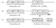
図2にバス上の転送フォーマットを示す。アドレスフェーズでは、アドレス、コマンドが順次送信され、これら全体に対するエラー訂正コード(以下、ECCコードという)が最後に付加される。又、アドレス及びコマンドにそれぞれECCコードを付加する場合もあるが、いずれにしても、アドレスフェーズはフォーマットが固定されている。
【0013】
しかし、データフェーズは図2(a),(b)に示すように、データ量が固定のシングルアクセスと、図2(c)に示すように、データ量が可変のバーストアクセスがある。シングルアクセスには、さらにデータ量の違いによって区別され、図2(a)に示すように、例えばデータ量32ビットに対してECCコードが付加されている場合と、図2(b)のように、データ量が2倍の64ビットに対してECCコードが付加されている場合の2つのシングルアクセスがある。又、バーストアクセスでは、図2(c)に示すように、データ量が可変なので、データとECCコードが分離されていない。
【0014】
データフェーズのフォーマットの違いを示す情報はアドレスフェーズのコマンドに入っており、スレーブはこの情報を基にデータフェーズのフォーマットを判断する。
【0015】
図3にモジュール内部の構成を示す。この実施形態ではバスマスタとスレーブの両方になり得るモジュールで各モジュールM1〜Mn,M11〜M1nが構成されている。又、バス結合用モジュールMa,Mbもこれらのモジュールと同一構成である。図3は、その1つのモジュール(モジュールM1〜Mn,M11〜M1n、バス結合用モジュールMa,Mbを代表してMと付している)の構成を示すものである。
各モジュールMには、送信側10と受信側11を備え、送信側10及び受信側11は内部バス12を介してモジュール間バス(1a,1b)又はシリアル伝送路に接続されている。
【0016】
送信側10には、アドレス/コマンドを受信してエラー検出/訂正コード(ECCコード)を生成する検出/訂正コード生成回路#A、シングル32ビットのデータを受信しエラー検出/訂正コード(ECCコード)を生成する検出/訂正コード生成回路#B、シングルでデータ幅が2倍の64ビットのデータを受信しエラー検出/訂正コード(ECCコード)を生成する検出/訂正コード生成回路#C、バーストのデータを受信しエラー検出/訂正コード(ECCコード)を生成する検出/訂正コード生成回路#D、及び送信側選択回路13を備える。
【0017】
アドレス、コマンド、各データ(シングルデータ、2倍のシングルデータ、バーストデータ)はそれぞれ内部バス12に送出され、かつ、送信側選択回路13によってその送出されたアドレス/コマンド、データの種類に基づいてECCコードがそれぞれ図2に示すように付されて、モジュール間バス1a,1b又はシリアル伝送路に送出される。
【0018】
一方、受信側11は、受信側選択回路14と、アドレス/コマンドのエラー検出/訂正を行うエラー検出/訂正回路#A、シングル32ビットのデータのエラー検出/訂正を行うエラー検出/訂正回路#B、シングルでデータ幅が2倍の64ビットのデータにおけるエラー検出/訂正を行うエラー検出/訂正回路#C、バーストデータのデータのエラー検出/訂正を行うエラー検出/訂正回路#Dを備える。モジュール間バス1a,1b又はシリアル伝送路を介して受信したアドレス/コマンド、データの種類に基づいて、受信側選択回路14によって、各エラー検出/訂正回路#A〜#Dに引き渡され、エラー検出/訂正がなされて、モジュールM内に取りこまれる。
【0019】
バスマスタがアドレス/コマンドを送信するアドレスフェーズの場合は、アドレス/コマンドフェーズ用のエラー検出/訂正コード生成回路#Aによって生成されたECCコードが送信側選択回路13によって選択され、該ECCコードが図2に示すようにアドレス/コマンドの後に付されて、モジュール間バス1a,1b又はシリアル伝送路に送出される。一方、バスマスタ以外のモジュールはアドレスフェーズを受信する際に受信側選択回路14によりアドレスフェーズ用のエラー検出/訂正回路#Aが選択され使用される。
【0020】
データフェーズではリードの場合はスレーブがデータを送信し、ライトの場合はバスマスタがデータを送信する。送信側のモジュールは、図2のような転送フォーマット毎に送信側10のエラー検出/訂正コード生成回路#A〜#Dを切り替え、バスに送信する。受信側のモジュールは、これに対応して受信側選択回路14でエラー検出/訂正回路#A〜#Dを選択切り替える。
【0021】
バスマスタが出力したアドレス/コマンドがライトの場合、受信側のスレーブのモジュールは、このアドレスフェーズで受信したコマンドの情報によって転送フォーマットを認識し、このコマンドで指令されている転送フォーマットに基づいて、受信側のモジュール(スレーブ)の受信側選択回路14は、データがシングル32ビットの場合は、エラー検出/訂正回路#Bに切り替え、データをシングル64ビットの場合は、エラー検出/訂正回路#Cに切り替え、バーストデータの場合には、エラー検出/訂正回路#Dに切り替えて、データを受信する。
【0022】
一方、バスマスタが出力したアドレス/コマンドがリードの場合、受信側のスレーブのモジュールは、このアドレスフェーズで受信したコマンドの情報によって転送フォーマットを認識し、この転送フォーマットに基づいて送信側選択回路13がエラー検出/訂正コード生成回路#B〜#Dを選択切り替え、リードしたデータを選択したエラー検出/訂正コード生成回路#B〜#Dで生成されたECCコードを図2に示すように、それぞれのデータにECCコードを付して送信する。このデータを受信するバスマスタのモジュールでは、アドレスフェーズでアドレス/コマンドを送出するときに、すでに、転送フォーマットを指定しているものであるから、このバスマスタのモジュールの受信側選択回路14は、指定した転送フォーマットに対応するエラー検出/訂正回路#B〜#Dを選択して切り替え、受信データのエラーの検出/訂正を行い、データを取りこむ。
【0023】
バス間を繋ぐシリアル伝送路においても同様に数種類の転送フォーマットを用意し、最適な回路でエラー検出/訂正を行うことができるようにエラー検出/訂正コード生成回路、又はエラー検出/訂正回路を切り替える。
【0024】
以上のように、本実施形態では、制御装置内でバスで接続されているモジュール間の通信において、各モジュールには、数種類の転送フォーマットに対応するエラー検出/訂正コード生成回路及びエラー検出/訂正回路を備えることによって、最適のデータ伝送を構成することができる。
【0025】
上述した実施形態では、アドレス/コマンド用の検出/訂正コード生成回路#A,エラー検出/訂正回路#A、データがシングル32ビット用の検出/訂正コード生成回路#B,エラー検出/訂正回路#B、データがシングル64ビット用の検出/訂正コード生成回路#C,エラー検出/訂正回路#C、バーストデータ用の検出/訂正コード生成回路#D,エラー検出/訂正回路#Dをモジュールに設けたが、これ以外にも、検査ビット長、情報ビット長、訂正能力に差異がある検出/訂正コード生成回路,エラー検出/訂正回路を設けて、必要とする最適なエラー検出/訂正方式を採用するようにすればよい。
【0026】
特に、アドレス、コマンド部分とデータ部分に対するエラー検出/訂正方式を変えることによって、固定長のアドレス、コマンド部分は大きなパケット単位でエラー検出/訂正を適用し、データ部分に比較してより検出/訂正能力を高めることができるようにすることができる。
【0027】
アドレス、コマンド部分に誤りが発生した場合、予期せぬ部位のデータを乱したり、システムとしてアクセスが許容されない資源に対するアクセスになり、重篤な障害を招く可能性があるため、この部分の誤り訂正/検出能力を高めることによってより高い信頼性が期待できる。
【0028】
またバスサイクルの一部に高い誤り訂正/検出能力を持つサイクルを含めることによって、万一バスにハード的な不具合が検出された場合に、その原因及び故障箇所を明確にすることが容易になる。例えばアドレス/コマンド部分には隣接2ビットの誤り検出、データ転送部分には1ビット誤り検出とした場合に、バスの隣接2ビットがショートしたケースにはシステムとして継続して動作することはできないが、バスのどの2ビットに不具合があったのかを明確にすることが可能となり、故障箇所や原因の解析に有効である。
【0029】
【発明の効果】
エラー検出・訂正機能が異なる複数のものの中から伝送する情報の内容、その量、その性質に応じて、最適なものを用いてデータの送受を行うことにより、信頼性の高いデータ伝送を行うことができる。
【図面の簡単な説明】
【図1】本発明のエラー検出/訂正方式を採用した一実施形態の制御装置の要部ブロック図である。
【図2】同実施形態におけるバス上の転送フォーマットの説明図である。
【図3】同実施形態におけるモジュールの一形態の要部ブロック図である。
【符号の説明】
M,M1〜Mn,M11〜M1n モジュール
Ma,Mb バス結合用モジュール
1a,1b バス
10 送信側
11 受信側
12 内部バス
13 送信側選択回路
14 受信側選択回路[0001]
BACKGROUND OF THE INVENTION
The present invention relates to an error detection / correction method in a bus connecting between modules of a control device and a control device using the method.
[0002]
[Prior art]
When data transmission is performed, a data error may be included in the transmission, and an error detection / correction code is used to detect and correct this data error. In general, the error detection / correction code has a higher detection / correction capability as the number of check bits increases. If the unit for performing error detection / correction increases, the detection / correction capability increases when the ratio of the check bits to the information bits is the same. .
[0003]
On the other hand, the bus transfer unit is an address and the command part has a fixed length, but the data part has various lengths. Therefore, due to this restriction, the size of the packet to be subjected to error detection / correction depends on the minimum transfer amount on the data side. Determined. Generally, it is limited to a low correction detection capability with respect to the ratio of check bits to information bits.
[0004]
In order to cope with fluctuations in the amount of data to be transmitted / received, an ECC (error correction code) used when the number of output bits of the memory element is small, particularly when the number of output bits of the memory element increases (n × k bits) There is known a data error detection apparatus that uses a plurality (k) of circuits (n bits) to detect the occurrence of a failure in a memory element (see Patent Document 1).
[0005]
Also, in a multi-origin / multi-target terminal switching system where messages are exchanged via fixed size bursts or cells, each terminal unit has an initial error correction code in the first burst of messages, a previous burst error correction code, and Also known are those that ensure the integrity of messages exchanged between data processing terminals by generating error correction codes as a function of burst data bytes and detecting errors compared to received burst error correction codes. (See Patent Document 2).
[0006]
[Patent Document 1]
JP-A-11-65944 (see paragraphs “0009” to “0011” and FIG. 1)
[Patent Document 2]
JP-A-6-53942 (see paragraph "0006")
[0007]
[Problems to be solved by the invention]
In the above-described method for detecting an error with respect to a data whose length changes, the method for dividing the data into the smallest units and detecting the error for each smallest unit has a constant detection / correction capability, and as described above. When the error detection / correction unit becomes large and the ratio of the inspection bits to the information bits is the same, the advantage of increased detection / correction capability cannot be enjoyed.
[0008]
SUMMARY OF THE INVENTION Accordingly, an object of the present invention is to provide an error detection / correction method for improving the optimum correction / detection capability and the method even if the size of a unit for error detection / correction changes or depending on the type of information. It is in providing the control apparatus which employ | adopted.
[0009]
[Means for Solving the Problems]
An error detection / correction method for data transmission between a plurality of bus-connected modules in a control device, wherein the invention according to
[0010]
The invention according to claim 5 is a control device using the error detection / correction system of the invention according to
[0011]
DETAILED DESCRIPTION OF THE INVENTION
FIG. 1 is a block diagram of an embodiment of a control device employing the error detection / correction of the present invention. A plurality of modules M1 to Mn are connected on the bus 1a. A plurality of modules M11 to M1n are also connected on the bus 1b. The bus 1a and the bus 1b are serially connected by bus coupling modules Ma and Mb. Each module can be a bus master or a slave. When the bus master obtains the right to use the bus, the bus master generates a bus cycle by outputting the access destination address, command, and the like. The state in which these pieces of information are output is called an address phase. Modules other than the bus master receive the information of the address phase and become slaves when it is determined that the access is for themselves, and exchange data between the master and the slave. This state in which data is exchanged is called a data phase.
[0012]
FIG. 2 shows a transfer format on the bus. In the address phase, addresses and commands are sequentially transmitted, and an error correction code (hereinafter referred to as ECC code) for all of them is added at the end. In some cases, an ECC code is added to each address and command, but in any case, the format of the address phase is fixed.
[0013]
However, the data phase includes single access with a fixed data amount as shown in FIGS. 2 (a) and 2 (b) and burst access with a variable data amount as shown in FIG. 2 (c). Single access is further distinguished by the difference in data amount. As shown in FIG. 2A, for example, when an ECC code is added to a data amount of 32 bits, as shown in FIG. There are two single accesses in the case where an ECC code is added to 64-bit data amount that is doubled. In the burst access, as shown in FIG. 2C, the data amount is variable, so that the data and the ECC code are not separated.
[0014]
Information indicating the difference in the format of the data phase is included in the address phase command, and the slave determines the format of the data phase based on this information.
[0015]
FIG. 3 shows the internal configuration of the module. In this embodiment, the modules M1 to Mn and M11 to M1n are configured by modules that can be both a bus master and a slave. The bus coupling modules Ma and Mb have the same configuration as these modules. FIG. 3 shows the configuration of one of the modules (modules M1 to Mn, M11 to M1n, bus coupling modules Ma and Mb are denoted by M).
Each module M includes a transmission side 10 and a
[0016]
The transmitting side 10 receives an address / command and generates an error detection / correction code (ECC code), a detection / correction code generation circuit #A, receives single 32-bit data, and receives an error detection / correction code (ECC code). Detection / correction code generation circuit #B, which generates a single 64-bit data having a double data width and generates an error detection / correction code (ECC code), burst The detection / correction code generation circuit #D for generating the error detection / correction code (ECC code) and the transmission side selection circuit 13 are provided.
[0017]
The address, command, and each data (single data, double single data, burst data) are sent to the
[0018]
On the other hand, the
[0019]
In the address phase in which the bus master transmits an address / command, the ECC code generated by the error detection / correction code generation circuit #A for the address / command phase is selected by the transmission side selection circuit 13, and the ECC code is shown in FIG. 2 is added after the address / command and sent to the inter-module buses 1a and 1b or the serial transmission path. On the other hand, when the module other than the bus master receives the address phase, the error detection / correction circuit #A for the address phase is selected and used by the receiving
[0020]
In the data phase, the slave transmits data in the case of reading, and the bus master transmits data in the case of writing. The transmission-side module switches the error detection / correction code generation circuits #A to #D on the transmission side 10 for each transfer format as shown in FIG. Correspondingly, the receiving side module selects and switches the error detection / correction circuits #A to #D by the receiving
[0021]
When the address / command output by the bus master is a write, the receiving slave module recognizes the transfer format based on the command information received in this address phase, and receives it based on the transfer format specified by this command. The reception
[0022]
On the other hand, when the address / command output by the bus master is a read, the receiving slave module recognizes the transfer format based on the command information received in this address phase, and the transmission side selection circuit 13 determines the transfer format based on this transfer format. The error detection / correction code generation circuits #B to #D are selectively switched, and the ECC codes generated by the error detection / correction code generation circuits #B to #D that select the read data are shown in FIG. Data is sent with an ECC code attached. In the bus master module that receives this data, when the address / command is sent in the address phase, the transfer format has already been specified. The error detection / correction circuits #B to #D corresponding to the transfer format are selected and switched to detect / correct errors in the received data and capture the data.
[0023]
Similarly, several types of transfer formats are prepared in the serial transmission path connecting the buses, and the error detection / correction code generation circuit or the error detection / correction circuit is switched so that error detection / correction can be performed with an optimum circuit. .
[0024]
As described above, in this embodiment, in communication between modules connected by a bus in the control device, each module has an error detection / correction code generation circuit and error detection / correction corresponding to several types of transfer formats. By providing the circuit, the optimum data transmission can be configured.
[0025]
In the embodiment described above, the address / command detection / correction code generation circuit #A, the error detection / correction circuit #A, the data detection / correction code generation circuit #B for single 32-bit data, and the error detection / correction circuit # B. Detection / correction code generation circuit #C for single 64-bit data, error detection / correction circuit #C, detection / correction code generation circuit #D for burst data, and error detection / correction circuit #D are provided in the module. However, in addition to this, a detection / correction code generation circuit and an error detection / correction circuit that differ in inspection bit length, information bit length, and correction capability are provided, and the optimum error detection / correction method required is adopted. You just have to do it.
[0026]
In particular, by changing the error detection / correction method for the address, command part, and data part, error detection / correction is applied to fixed-length addresses and command parts in units of large packets, and they are detected / corrected more than the data part. The ability can be increased.
[0027]
If an error occurs in the address or command part, data in an unexpected part may be disturbed, or access to a resource that is not permitted to be accessed by the system may result, resulting in a serious failure. Higher reliability can be expected by increasing the correction / detection capability.
[0028]
In addition, by including a cycle with high error correction / detection capability in a part of the bus cycle, if a hardware failure is detected in the bus, it becomes easy to clarify the cause and failure location. . For example, when the adjacent 2 bits are detected in the address / command part and the 1 bit error is detected in the data transfer part, the system cannot continue to operate when the adjacent 2 bits of the bus are short-circuited. This makes it possible to clarify which 2 bits of the bus are defective, and is effective in analyzing the failure location and the cause.
[0029]
【The invention's effect】
Highly reliable data transmission by sending and receiving data using the most appropriate information according to the content, amount, and nature of information to be transmitted from multiple items with different error detection / correction functions Can do.
[Brief description of the drawings]
FIG. 1 is a block diagram of a main part of a control device according to an embodiment adopting an error detection / correction method of the present invention.
FIG. 2 is an explanatory diagram of a transfer format on the bus in the embodiment;
FIG. 3 is a block diagram showing a main part of one form of a module according to the embodiment;
[Explanation of symbols]
M, M1 to Mn, M11 to M1n Module Ma, Mb Bus coupling module 1a, 1b Bus 10
Claims (6)
Priority Applications (3)
| Application Number | Priority Date | Filing Date | Title |
|---|---|---|---|
| JP2002355634A JP3757204B2 (en) | 2002-12-06 | 2002-12-06 | Error detection / correction method and control device using the method |
| EP03257609A EP1427126B1 (en) | 2002-12-06 | 2003-12-03 | Error detection/correction system, and controller using this system |
| US10/726,561 US7428686B2 (en) | 2002-12-06 | 2003-12-04 | Error detection/correction system, and controller using this system |
Applications Claiming Priority (1)
| Application Number | Priority Date | Filing Date | Title |
|---|---|---|---|
| JP2002355634A JP3757204B2 (en) | 2002-12-06 | 2002-12-06 | Error detection / correction method and control device using the method |
Publications (2)
| Publication Number | Publication Date |
|---|---|
| JP2004193664A JP2004193664A (en) | 2004-07-08 |
| JP3757204B2 true JP3757204B2 (en) | 2006-03-22 |
Family
ID=32310768
Family Applications (1)
| Application Number | Title | Priority Date | Filing Date |
|---|---|---|---|
| JP2002355634A Expired - Fee Related JP3757204B2 (en) | 2002-12-06 | 2002-12-06 | Error detection / correction method and control device using the method |
Country Status (3)
| Country | Link |
|---|---|
| US (1) | US7428686B2 (en) |
| EP (1) | EP1427126B1 (en) |
| JP (1) | JP3757204B2 (en) |
Families Citing this family (12)
| Publication number | Priority date | Publication date | Assignee | Title |
|---|---|---|---|---|
| US20060195631A1 (en) | 2005-01-31 | 2006-08-31 | Ramasubramanian Rajamani | Memory buffers for merging local data from memory modules |
| US7827462B2 (en) | 2005-03-31 | 2010-11-02 | Intel Corporation | Combined command and data code |
| CN101176289B (en) * | 2005-05-13 | 2012-11-14 | 费希尔-罗斯蒙德系统公司 | Fieldbus process communications using error correction |
| JP4226620B2 (en) * | 2006-08-24 | 2009-02-18 | ファナック株式会社 | Data transfer method and data transfer device |
| FR2917863A1 (en) * | 2007-06-20 | 2008-12-26 | St Microelectronics Crolles 2 | Data bus for portable electronic devices e.g. mobile phone, has repeater logical blocks with logical error correction circuit coupled with repeater in parallel, where circuit is arranged for determining error correction bit |
| KR20120137416A (en) | 2010-03-22 | 2012-12-20 | 모사이드 테크놀로지스 인코퍼레이티드 | Composite semiconductor memory device with error correction |
| JP2012257122A (en) * | 2011-06-09 | 2012-12-27 | Hitachi Automotive Systems Ltd | Vehicle controller and vehicle control system |
| JP2013062691A (en) * | 2011-09-13 | 2013-04-04 | Dainippon Printing Co Ltd | Information processing device and computer program |
| KR101829464B1 (en) * | 2011-10-13 | 2018-04-11 | 삼성전자주식회사 | Method and apparatus for encoding of pacekt data |
| CN108197199B (en) * | 2017-12-27 | 2021-10-29 | 珠海市君天电子科技有限公司 | Data monitoring method and device, electronic equipment and computer readable storage medium |
| JP7428689B2 (en) | 2021-12-17 | 2024-02-06 | 華邦電子股▲ふん▼有限公司 | memory system |
| KR102645215B1 (en) * | 2022-01-27 | 2024-03-07 | 윈본드 일렉트로닉스 코포레이션 | Memory system |
Family Cites Families (16)
| Publication number | Priority date | Publication date | Assignee | Title |
|---|---|---|---|---|
| US4228496A (en) * | 1976-09-07 | 1980-10-14 | Tandem Computers Incorporated | Multiprocessor system |
| US4453213A (en) * | 1981-07-30 | 1984-06-05 | Harris Corporation | Error reporting scheme |
| JP3003277B2 (en) * | 1991-05-24 | 2000-01-24 | ソニー株式会社 | Digital data communication method and apparatus |
| US5638386A (en) * | 1991-09-20 | 1997-06-10 | Hitachi, Ltd. | Recording apparatus |
| JPH05158808A (en) | 1991-12-06 | 1993-06-25 | Nec Eng Ltd | Microprogram controller |
| US5539754A (en) * | 1992-10-05 | 1996-07-23 | Hewlett-Packard Company | Method and circuitry for generating syndrome bits within an error correction and detection circuit |
| EP0606016B1 (en) * | 1993-01-07 | 2002-10-09 | Kabushiki Kaisha Toshiba | Data communication system using an adaptive hybrid ARQ scheme |
| EP0608663B1 (en) * | 1993-01-25 | 1999-03-10 | Bull HN Information Systems Italia S.p.A. | A multi-processor system with shared memory |
| JP2885263B2 (en) * | 1993-09-30 | 1999-04-19 | 日本ビクター株式会社 | Code generation method |
| US5535405A (en) * | 1993-12-23 | 1996-07-09 | Unisys Corporation | Microsequencer bus controller system |
| JPH0853942A (en) | 1994-08-12 | 1996-02-27 | Fujita Corp | PC floor board hanging jig and PC floor board laying method using this jig |
| US5570425A (en) * | 1994-11-07 | 1996-10-29 | Digisonix, Inc. | Transducer daisy chain |
| US6415398B1 (en) * | 1995-09-29 | 2002-07-02 | Kabushiki Kaisha Toshiba | Coding system and decoding system |
| WO1998001806A1 (en) | 1996-07-03 | 1998-01-15 | Hitachi, Ltd. | Information processor |
| JPH1165944A (en) | 1997-08-13 | 1999-03-09 | Fujitsu Ltd | Data error detection device |
| US6745268B1 (en) * | 2000-08-11 | 2004-06-01 | Micron Technology, Lnc. | Capacitive multidrop bus compensation |
-
2002
- 2002-12-06 JP JP2002355634A patent/JP3757204B2/en not_active Expired - Fee Related
-
2003
- 2003-12-03 EP EP03257609A patent/EP1427126B1/en not_active Expired - Lifetime
- 2003-12-04 US US10/726,561 patent/US7428686B2/en not_active Expired - Lifetime
Also Published As
| Publication number | Publication date |
|---|---|
| EP1427126B1 (en) | 2011-11-16 |
| US7428686B2 (en) | 2008-09-23 |
| JP2004193664A (en) | 2004-07-08 |
| US20040153939A1 (en) | 2004-08-05 |
| EP1427126A3 (en) | 2006-10-04 |
| EP1427126A2 (en) | 2004-06-09 |
Similar Documents
| Publication | Publication Date | Title |
|---|---|---|
| CN100470496C (en) | Channel testing with mutable maps | |
| CN100498724C (en) | Early CRC delivery for partial frame | |
| JP4210302B2 (en) | Memory channel with unidirectional link | |
| JP4210300B2 (en) | Memory channels that can be added / removed while the power is on | |
| US7047475B2 (en) | CRC encoding scheme for conveying status information | |
| JP4210301B2 (en) | Memory channels that use transposed state patterns | |
| JP3757204B2 (en) | Error detection / correction method and control device using the method | |
| US12120010B2 (en) | Error detection test device for a subscriber station of a serial bus system and method for testing mechanisms for detecting errors in a communication in a serial bus system | |
| US20150019936A1 (en) | Error detection method and a system including one or more memory device | |
| KR101687038B1 (en) | Error detection method and a system including one or more memory devices | |
| JP2007511012A (en) | Data storage between data path and memory device | |
| JP2006526849A (en) | Memory channel with bit lane failover | |
| US7810013B2 (en) | Memory device that reflects back error detection signals | |
| US20050201162A1 (en) | Data transfer control device and electronic instrument | |
| US6157651A (en) | Rogue data packet removal method and apparatus | |
| CN118381721B (en) | Method for configuring serializer or sensor by I2C broadcast in A-PHY system | |
| KR100717572B1 (en) | Control method for error detection and correction apparatus, error detection and correction apparatus, and control program for error detection and correction apparatus | |
| CN101189593A (en) | Method for transmitting redundant data during address transmission on a multiplexed address/data bus | |
| Creech | Black Channel Communication: What is it and how does it work? | |
| US20070008907A1 (en) | Reconfigurable LSI | |
| US7596742B1 (en) | Error detection in a communication link | |
| WO2025009346A1 (en) | Semiconductor device and communication system | |
| CN119046227A (en) | Data transmission module and data transmission method | |
| KR19980048995A (en) | Data transmission apparatus and method | |
| JPH02287744A (en) | Bus master device |
Legal Events
| Date | Code | Title | Description |
|---|---|---|---|
| A977 | Report on retrieval |
Free format text: JAPANESE INTERMEDIATE CODE: A971007 Effective date: 20050120 |
|
| A131 | Notification of reasons for refusal |
Free format text: JAPANESE INTERMEDIATE CODE: A131 Effective date: 20050126 |
|
| A131 | Notification of reasons for refusal |
Free format text: JAPANESE INTERMEDIATE CODE: A131 Effective date: 20050531 |
|
| A521 | Request for written amendment filed |
Free format text: JAPANESE INTERMEDIATE CODE: A523 Effective date: 20050711 |
|
| TRDD | Decision of grant or rejection written | ||
| A01 | Written decision to grant a patent or to grant a registration (utility model) |
Free format text: JAPANESE INTERMEDIATE CODE: A01 Effective date: 20051213 |
|
| A61 | First payment of annual fees (during grant procedure) |
Free format text: JAPANESE INTERMEDIATE CODE: A61 Effective date: 20051226 |
|
| R150 | Certificate of patent or registration of utility model |
Free format text: JAPANESE INTERMEDIATE CODE: R150 Ref document number: 3757204 Country of ref document: JP Free format text: JAPANESE INTERMEDIATE CODE: R150 |
|
| FPAY | Renewal fee payment (event date is renewal date of database) |
Free format text: PAYMENT UNTIL: 20100106 Year of fee payment: 4 |
|
| FPAY | Renewal fee payment (event date is renewal date of database) |
Free format text: PAYMENT UNTIL: 20110106 Year of fee payment: 5 |
|
| FPAY | Renewal fee payment (event date is renewal date of database) |
Free format text: PAYMENT UNTIL: 20120106 Year of fee payment: 6 |
|
| FPAY | Renewal fee payment (event date is renewal date of database) |
Free format text: PAYMENT UNTIL: 20120106 Year of fee payment: 6 |
|
| FPAY | Renewal fee payment (event date is renewal date of database) |
Free format text: PAYMENT UNTIL: 20130106 Year of fee payment: 7 |
|
| FPAY | Renewal fee payment (event date is renewal date of database) |
Free format text: PAYMENT UNTIL: 20130106 Year of fee payment: 7 |
|
| FPAY | Renewal fee payment (event date is renewal date of database) |
Free format text: PAYMENT UNTIL: 20140106 Year of fee payment: 8 |
|
| LAPS | Cancellation because of no payment of annual fees |