CN107667421B - Substrate processing apparatus disposed in a process chamber and method of operating the same - Google Patents
Substrate processing apparatus disposed in a process chamber and method of operating the same Download PDFInfo
- Publication number
- CN107667421B CN107667421B CN201680027285.5A CN201680027285A CN107667421B CN 107667421 B CN107667421 B CN 107667421B CN 201680027285 A CN201680027285 A CN 201680027285A CN 107667421 B CN107667421 B CN 107667421B
- Authority
- CN
- China
- Prior art keywords
- magnet
- disk
- metal ring
- axis
- processing apparatus
- Prior art date
- Legal status (The legal status is an assumption and is not a legal conclusion. Google has not performed a legal analysis and makes no representation as to the accuracy of the status listed.)
- Active
Links
Images


Classifications
-
- H—ELECTRICITY
- H01—ELECTRIC ELEMENTS
- H01L—SEMICONDUCTOR DEVICES NOT COVERED BY CLASS H10
- H01L21/00—Processes or apparatus adapted for the manufacture or treatment of semiconductor or solid state devices or of parts thereof
- H01L21/67—Apparatus specially adapted for handling semiconductor or electric solid state devices during manufacture or treatment thereof; Apparatus specially adapted for handling wafers during manufacture or treatment of semiconductor or electric solid state devices or components ; Apparatus not specifically provided for elsewhere
- H01L21/683—Apparatus specially adapted for handling semiconductor or electric solid state devices during manufacture or treatment thereof; Apparatus specially adapted for handling wafers during manufacture or treatment of semiconductor or electric solid state devices or components ; Apparatus not specifically provided for elsewhere for supporting or gripping
- H01L21/687—Apparatus specially adapted for handling semiconductor or electric solid state devices during manufacture or treatment thereof; Apparatus specially adapted for handling wafers during manufacture or treatment of semiconductor or electric solid state devices or components ; Apparatus not specifically provided for elsewhere for supporting or gripping using mechanical means, e.g. chucks, clamps or pinches
- H01L21/68714—Apparatus specially adapted for handling semiconductor or electric solid state devices during manufacture or treatment thereof; Apparatus specially adapted for handling wafers during manufacture or treatment of semiconductor or electric solid state devices or components ; Apparatus not specifically provided for elsewhere for supporting or gripping using mechanical means, e.g. chucks, clamps or pinches the wafers being placed on a susceptor, stage or support
-
- H—ELECTRICITY
- H01—ELECTRIC ELEMENTS
- H01L—SEMICONDUCTOR DEVICES NOT COVERED BY CLASS H10
- H01L21/00—Processes or apparatus adapted for the manufacture or treatment of semiconductor or solid state devices or of parts thereof
- H01L21/67—Apparatus specially adapted for handling semiconductor or electric solid state devices during manufacture or treatment thereof; Apparatus specially adapted for handling wafers during manufacture or treatment of semiconductor or electric solid state devices or components ; Apparatus not specifically provided for elsewhere
- H01L21/67005—Apparatus not specifically provided for elsewhere
- H01L21/67011—Apparatus for manufacture or treatment
- H01L21/67155—Apparatus for manufacturing or treating in a plurality of work-stations
- H01L21/6719—Apparatus for manufacturing or treating in a plurality of work-stations characterized by the construction of the processing chambers, e.g. modular processing chambers
-
- H—ELECTRICITY
- H01—ELECTRIC ELEMENTS
- H01L—SEMICONDUCTOR DEVICES NOT COVERED BY CLASS H10
- H01L21/00—Processes or apparatus adapted for the manufacture or treatment of semiconductor or solid state devices or of parts thereof
- H01L21/67—Apparatus specially adapted for handling semiconductor or electric solid state devices during manufacture or treatment thereof; Apparatus specially adapted for handling wafers during manufacture or treatment of semiconductor or electric solid state devices or components ; Apparatus not specifically provided for elsewhere
- H01L21/683—Apparatus specially adapted for handling semiconductor or electric solid state devices during manufacture or treatment thereof; Apparatus specially adapted for handling wafers during manufacture or treatment of semiconductor or electric solid state devices or components ; Apparatus not specifically provided for elsewhere for supporting or gripping
- H01L21/687—Apparatus specially adapted for handling semiconductor or electric solid state devices during manufacture or treatment thereof; Apparatus specially adapted for handling wafers during manufacture or treatment of semiconductor or electric solid state devices or components ; Apparatus not specifically provided for elsewhere for supporting or gripping using mechanical means, e.g. chucks, clamps or pinches
- H01L21/68714—Apparatus specially adapted for handling semiconductor or electric solid state devices during manufacture or treatment thereof; Apparatus specially adapted for handling wafers during manufacture or treatment of semiconductor or electric solid state devices or components ; Apparatus not specifically provided for elsewhere for supporting or gripping using mechanical means, e.g. chucks, clamps or pinches the wafers being placed on a susceptor, stage or support
- H01L21/68764—Apparatus specially adapted for handling semiconductor or electric solid state devices during manufacture or treatment thereof; Apparatus specially adapted for handling wafers during manufacture or treatment of semiconductor or electric solid state devices or components ; Apparatus not specifically provided for elsewhere for supporting or gripping using mechanical means, e.g. chucks, clamps or pinches the wafers being placed on a susceptor, stage or support characterised by a movable susceptor, stage or support, others than those only rotating on their own vertical axis, e.g. susceptors on a rotating caroussel
-
- H—ELECTRICITY
- H01—ELECTRIC ELEMENTS
- H01L—SEMICONDUCTOR DEVICES NOT COVERED BY CLASS H10
- H01L21/00—Processes or apparatus adapted for the manufacture or treatment of semiconductor or solid state devices or of parts thereof
- H01L21/67—Apparatus specially adapted for handling semiconductor or electric solid state devices during manufacture or treatment thereof; Apparatus specially adapted for handling wafers during manufacture or treatment of semiconductor or electric solid state devices or components ; Apparatus not specifically provided for elsewhere
- H01L21/683—Apparatus specially adapted for handling semiconductor or electric solid state devices during manufacture or treatment thereof; Apparatus specially adapted for handling wafers during manufacture or treatment of semiconductor or electric solid state devices or components ; Apparatus not specifically provided for elsewhere for supporting or gripping
- H01L21/687—Apparatus specially adapted for handling semiconductor or electric solid state devices during manufacture or treatment thereof; Apparatus specially adapted for handling wafers during manufacture or treatment of semiconductor or electric solid state devices or components ; Apparatus not specifically provided for elsewhere for supporting or gripping using mechanical means, e.g. chucks, clamps or pinches
- H01L21/68714—Apparatus specially adapted for handling semiconductor or electric solid state devices during manufacture or treatment thereof; Apparatus specially adapted for handling wafers during manufacture or treatment of semiconductor or electric solid state devices or components ; Apparatus not specifically provided for elsewhere for supporting or gripping using mechanical means, e.g. chucks, clamps or pinches the wafers being placed on a susceptor, stage or support
- H01L21/68771—Apparatus specially adapted for handling semiconductor or electric solid state devices during manufacture or treatment thereof; Apparatus specially adapted for handling wafers during manufacture or treatment of semiconductor or electric solid state devices or components ; Apparatus not specifically provided for elsewhere for supporting or gripping using mechanical means, e.g. chucks, clamps or pinches the wafers being placed on a susceptor, stage or support characterised by supporting more than one semiconductor substrate
-
- H—ELECTRICITY
- H01—ELECTRIC ELEMENTS
- H01L—SEMICONDUCTOR DEVICES NOT COVERED BY CLASS H10
- H01L21/00—Processes or apparatus adapted for the manufacture or treatment of semiconductor or solid state devices or of parts thereof
- H01L21/67—Apparatus specially adapted for handling semiconductor or electric solid state devices during manufacture or treatment thereof; Apparatus specially adapted for handling wafers during manufacture or treatment of semiconductor or electric solid state devices or components ; Apparatus not specifically provided for elsewhere
- H01L21/683—Apparatus specially adapted for handling semiconductor or electric solid state devices during manufacture or treatment thereof; Apparatus specially adapted for handling wafers during manufacture or treatment of semiconductor or electric solid state devices or components ; Apparatus not specifically provided for elsewhere for supporting or gripping
- H01L21/687—Apparatus specially adapted for handling semiconductor or electric solid state devices during manufacture or treatment thereof; Apparatus specially adapted for handling wafers during manufacture or treatment of semiconductor or electric solid state devices or components ; Apparatus not specifically provided for elsewhere for supporting or gripping using mechanical means, e.g. chucks, clamps or pinches
- H01L21/68714—Apparatus specially adapted for handling semiconductor or electric solid state devices during manufacture or treatment thereof; Apparatus specially adapted for handling wafers during manufacture or treatment of semiconductor or electric solid state devices or components ; Apparatus not specifically provided for elsewhere for supporting or gripping using mechanical means, e.g. chucks, clamps or pinches the wafers being placed on a susceptor, stage or support
- H01L21/68785—Apparatus specially adapted for handling semiconductor or electric solid state devices during manufacture or treatment thereof; Apparatus specially adapted for handling wafers during manufacture or treatment of semiconductor or electric solid state devices or components ; Apparatus not specifically provided for elsewhere for supporting or gripping using mechanical means, e.g. chucks, clamps or pinches the wafers being placed on a susceptor, stage or support characterised by the mechanical construction of the susceptor, stage or support
-
- H—ELECTRICITY
- H01—ELECTRIC ELEMENTS
- H01L—SEMICONDUCTOR DEVICES NOT COVERED BY CLASS H10
- H01L21/00—Processes or apparatus adapted for the manufacture or treatment of semiconductor or solid state devices or of parts thereof
- H01L21/67—Apparatus specially adapted for handling semiconductor or electric solid state devices during manufacture or treatment thereof; Apparatus specially adapted for handling wafers during manufacture or treatment of semiconductor or electric solid state devices or components ; Apparatus not specifically provided for elsewhere
- H01L21/683—Apparatus specially adapted for handling semiconductor or electric solid state devices during manufacture or treatment thereof; Apparatus specially adapted for handling wafers during manufacture or treatment of semiconductor or electric solid state devices or components ; Apparatus not specifically provided for elsewhere for supporting or gripping
- H01L21/687—Apparatus specially adapted for handling semiconductor or electric solid state devices during manufacture or treatment thereof; Apparatus specially adapted for handling wafers during manufacture or treatment of semiconductor or electric solid state devices or components ; Apparatus not specifically provided for elsewhere for supporting or gripping using mechanical means, e.g. chucks, clamps or pinches
- H01L21/68714—Apparatus specially adapted for handling semiconductor or electric solid state devices during manufacture or treatment thereof; Apparatus specially adapted for handling wafers during manufacture or treatment of semiconductor or electric solid state devices or components ; Apparatus not specifically provided for elsewhere for supporting or gripping using mechanical means, e.g. chucks, clamps or pinches the wafers being placed on a susceptor, stage or support
- H01L21/68792—Apparatus specially adapted for handling semiconductor or electric solid state devices during manufacture or treatment thereof; Apparatus specially adapted for handling wafers during manufacture or treatment of semiconductor or electric solid state devices or components ; Apparatus not specifically provided for elsewhere for supporting or gripping using mechanical means, e.g. chucks, clamps or pinches the wafers being placed on a susceptor, stage or support characterised by the construction of the shaft
Abstract
Disclosed is a substrate processing apparatus including: a disk provided to be rotatable on an axis thereof; at least one susceptor arranged on the disk such that a substrate is placed on an upper surface of the susceptor, the susceptor being configured to rotate on an axis thereof and revolve around a center of the disk as the disk rotates on the axis thereof; a metal ring connected to a lower portion of the base, the metal ring being disposed such that a center thereof coincides with a center of the base; and a magnet disposed under the disk to be radially arranged based on a center of the disk, at least a portion of the magnet being opposite to the metal ring in a vertical direction.
Description
Technical Field
The present invention relates to a substrate processing apparatus disposed in a process chamber and an operating method thereof.
Background
The statements in this section merely provide background information related to the present disclosure and may not constitute prior art.
In general, a semiconductor memory device, a liquid crystal display apparatus, an organic light emitting apparatus, and the like are manufactured by performing various semiconductor processes on a substrate to deposit and stack into a structure having a desired shape.
Examples of semiconductor processing include a process of depositing a specified thin film on a substrate, a photolithography process of exposing selected regions of the thin film to light, and an etching process of removing the thin film from the selected regions. These semiconductor processes are performed in process chambers, in which an optimal environment is created for the respective process.
Generally, an apparatus for processing a circular substrate (e.g., a wafer) is placed in the processing chamber and is configured such that a plurality of circular susceptors are mounted on a circular disk, which is larger than the susceptors.
In the substrate processing apparatus, after a substrate is placed on the susceptor, the disk is rotated on its axis, and the susceptor is rotated on its axis and also revolves around the center of the disk. Then, the processing of the substrate is performed in such a way that the source material is sprayed on the substrate so that a structure having a desired shape can be deposited, laminated or etched on the substrate.
At this time, an additional means for injecting air or other gas is used so as to allow the susceptor to rotate on its axis. In this scheme, foreign substances contained in the air or gas may be inconveniently absorbed onto the substrate, resulting in a defective product.
Disclosure of Invention
Technical problem
It is, therefore, an object of the present invention to provide a substrate processing apparatus, which is disposed in a process chamber and rotates a susceptor about its axis without using an additional device for injecting air or other gas, and an associated operating method thereof.
The technical objects to be achieved by the present invention are not limited to the above-mentioned technical objects, and other technical objects not mentioned will be clearly understood by those of ordinary skill in the art from the following description.
Technical scheme
In one embodiment, a substrate processing apparatus includes: a disc provided to be rotatable on an axis thereof; at least one susceptor arranged on the disk such that a substrate is placed on an upper surface of the susceptor, the susceptor being configured to rotate on an axis thereof and revolve around a center of the disk as the disk rotates on the axis thereof; a metal ring connected to a lower portion of the base, the metal ring being disposed such that a center thereof coincides with a center of the base; and a magnet disposed below the disk to be radially arranged based on a center of the disk, at least a portion of the magnet being vertically opposite to the metal ring.
In this embodiment, the substrate processing apparatus may further include: a bearing disposed in contact with both the disk and the base; and a frame having a receiving portion for receiving the disk, and the metal ring is rotatable on its axis by a magnetic force of the magnet as the disk rotates on its axis, thereby rotating the base on its axis.
In this embodiment, the base may include a first support portion protruding from a lower surface thereof, the first support portion being connected to the metal ring and configured to support the bearing.
The metal ring may include an inner ring connected to the first support portion, an outer ring connected to the inner ring, and a ring connecting portion formed between the outer ring and the inner ring to connect the outer ring and the inner ring to each other.
The outer ring may be vertically opposite to the magnet, and may have a width greater than that of the magnet.
The outer ring may be vertically opposite the magnet and may include a region opposite the magnet for covering the entire magnet in the vertical direction.
The magnet may be radially arranged on the frame based on a center of the receiving portion so as not to rotate.
The magnet may comprise a plurality of segments arranged radially at fixed intervals.
The segments may have a cylindrical shape.
In this embodiment, the substrate processing apparatus may further include a shaft inserted into a through hole formed in a central region of the receiving part for rotating the coil around an axis thereof; and a disk support portion having a lower side connected to an upper end of the shaft and an upper side connected to the disk.
In this embodiment, the speed at which the base rotates on its axis may be proportional to the ratio of the diameter of the metal ring to the diameter of the magnet.
The diameter of the magnet may be a value obtained by measuring a distance between opposite points on the width center of the magnet arranged in a ring shape in a diameter direction, and the diameter of the metal ring may be a value obtained by measuring a distance between opposite points on the width center of the metal ring in a diameter direction.
The metal ring may be made of a ferromagnetic material.
The direction in which the disc rotates on its axis may be the same as the direction in which the base rotates on its axis.
A center of the magnet disposed under the disk and radially arranged based on the center of the disk may be spaced apart from a center of the metal ring.
In another embodiment, a substrate processing apparatus includes: a disc configured to be rotatable; a susceptor disposed on the disk so that a substrate is placed on an upper surface thereof, the susceptor being configured to rotate on an axis thereof and revolve around a center of the disk as the disk rotates; a metal ring connected to a lower portion of the base, the metal ring being arranged such that a center thereof coincides with a center of the base; and a magnet disposed under the disk so as to be radially arranged based on a center of the disk, the magnet being opposite to the metal ring in a vertical direction, wherein the base rotates on an axis thereof in a same direction as a direction in which the disk rotates on the axis thereof as the disk rotates on the axis thereof.
The metal ring may include a region for covering the entire magnet in a ring shape in a vertical direction.
In another embodiment, a substrate processing apparatus includes: a disc configured to be rotatable; a susceptor disposed on the disk so that a substrate is placed on an upper surface thereof, the susceptor being configured to rotate on an axis thereof and revolve around a center of the disk as the disk rotates; a metal ring connected to a lower portion of the base, the metal ring being arranged such that a center thereof coincides with a center of the base; and a magnet disposed under the disk to be radially arranged based on a center of the disk, the magnet being opposite to the metal ring in a vertical direction, wherein a speed at which the susceptor rotates on an axis thereof is proportional to a ratio of a diameter of the metal ring to a diameter of the magnet.
In another embodiment, a substrate processing apparatus includes: a disk configured to perform a first rotation; at least one susceptor arranged on the disk such that a substrate is placed on an upper surface thereof, the susceptor being configured to perform the first rotation and perform a second rotation about a center of the disk as the disk performs the first rotation; a metal ring connected to a lower portion of the base, the metal ring being arranged such that a center thereof coincides with a center of the base; and a magnet disposed below the disk to be radially arranged based on a center of the disk, at least a portion of the magnet being vertically opposite to the metal ring.
In another embodiment, a method of operating a substrate processing apparatus includes: rotating the disk on its axis, revolving a base around a center of the disk as the disk rotates on its axis, revolving a metal ring around the center of the disk as the base revolves around the center of the disk, the metal ring being connected with a lower portion of the base, magnetically attracting the metal ring with a magnet, the metal ring and the magnet being opposed to each other in a vertical direction, and the base connected with the metal ring being attracted and rotated on its axis by the magnet due to a magnetic attraction force between the magnet and the metal ring.
Advantageous effects
According to the present invention, since the susceptor can be rotated on its axis without an additional susceptor rotating apparatus using air or gas, the configuration of the substrate processing apparatus can be simplified and power consumption required for processing the substrate can be reduced.
In addition, it is possible to significantly reduce the occurrence of defective products caused when foreign substances contained in air or gas are absorbed on, for example, a substrate (such as a wafer) when using a rotating apparatus using air or gas.
Further, by suppressing vibration and noise generated during rotation of the susceptor, it is possible to suppress generation of vibration of the substrate placed on the upper surface of the susceptor, uneven deposition on the substrate, and erosion.
Drawings
Fig. 1 is a cross-sectional perspective view showing a substrate processing apparatus according to an embodiment.
Fig. 2 is a sectional view showing a portion a of fig. 1.
Fig. 3 and 4 are schematic bottom views for explaining the operation of the tray and the base according to one embodiment.
Fig. 5 is a cross-sectional perspective view showing a part of a substrate processing apparatus according to an embodiment.
Fig. 6 is a plan view showing a metal ring according to an embodiment.
Fig. 7 is a view for explaining an arrangement of a metal ring and a magnet according to an embodiment.
Fig. 8 is a flowchart for explaining an operation method of a substrate processing apparatus according to an embodiment.
Fig. 9 is a schematic sectional view showing a substrate processing apparatus according to another embodiment.
Fig. 10 is a schematic sectional view showing a substrate processing apparatus according to still another embodiment.
Detailed Description
Various embodiments will be described in detail below with reference to the accompanying drawings. The described embodiments may be modified in many different ways and may take many different forms, and specific embodiments have been shown in the drawings and will be described in detail below. It should be understood, however, that the drawings and description thereto are not intended to limit the embodiments to the particular form disclosed, but on the contrary, the intention is to cover all modifications, equivalents, and alternatives falling within the spirit and scope of the present embodiments. Herein, the size or shape of each element shown in the drawings may be exaggerated for clarity and convenience.
The terms "first," "second," and the like may be used to describe various elements, but the elements should not be limited by the terms. The term is used only to distinguish one element from another. In addition, terms specifically defined in consideration of the configuration and operation of the respective embodiments are only used to describe the embodiments, and are not intended to show the scope of the respective embodiments.
In describing the various embodiments, it will be understood that when an element is referred to as being "on" or "under" another element, it can be "directly on or under the other element or" indirectly on the other element, such that intervening elements may also be present. Further, it will be understood that when an element is referred to as being "on" or "under" another element, it can be referred to as being "above" or "below" the other element.
Furthermore, the relative terms "top/over," "bottom/under" and the like in the description and the claims may be used for distinguishing between one substance or element and another substance or element and not necessarily for describing a physical or logical relationship between the substances or elements or a particular order.
Fig. 1 is a cross-sectional perspective view showing a substrate processing apparatus according to an embodiment. Fig. 2 is a sectional view showing a portion a of fig. 1. The substrate processing apparatus of this embodiment includes a disk 100, a susceptor 200, a metal ring 300, a magnet 400, a bearing 600, and a frame 500.
The disc 100 may be received in a receiving portion 510 defined in the frame 500 so as to perform a first rotation, i.e., a rotation on its axis with respect to the frame 500. The pedestals 200 may be symmetrically arranged on the disc 100 based on the center of the disc 100. The base 200 will be described in detail below.
The tray 100 may be mounted on a frame 500, as shown in fig. 1. At this time, the receiving part 510 may be formed in the frame 500 such that the area and shape thereof correspond to the shape and area of the disc 100, so that the disc 100 may be placed in the receiving part 510.
Meanwhile, in the case where the base 200 is provided on the disc 100, a different number of bases 200 may be radially arranged on the disc 100 depending on the size of the base 200. Further, a tray placement region may be depressed in the upper portion of the tray 100 to form a region and a shape corresponding to those of the base 200, so that the base 200 may be placed in the tray placement region.
The susceptor 200 may be placed on the tray 100 and may be configured such that a substrate is placed on an upper surface thereof. As the disk 100 rotates on its axis, the base 200 may rotate on its axis, and may also perform a second rotation, i.e., a revolution around the center of the disk 100. At this time, the base 200 may be rotated on its axis by a magnetic force acting between the metal ring 300 and the magnet 400.
A substrate (not shown) may be placed on the upper surface of the susceptor 200. At this time, in the case where the susceptor 200 has a circular shape as in this embodiment, the substrate may be, for example, a circular wafer. Accordingly, a substrate (e.g., a wafer) placed on the upper surface of the susceptor 200 may be processed by injecting a process gas, e.g., including a source material, onto the substrate.
Further, since the susceptor 200 is rotated on its axis while being revolved around the center of the disk 100, a film may be deposited or etched on a circular substrate placed on the susceptor 200 so as to be symmetrical in a diameter direction based on the center of the circular substrate.
Meanwhile, the first support part 210 may be located below the base 200. The first support part 210 may protrude from the lower surface of the base 200, may be connected with the metal ring 300, and may be used to support the bearing 600.
As shown in fig. 2, the first support part 210 may protrude from the lower surface of the base 200 and may define a recess into which the connector P may be inserted. Meanwhile, the metal ring 300 may provide a hole in a region thereof for connection with the first support part 210, into which the connection member P may be inserted.
Meanwhile, a plurality of connection members P may be radially connected to the metal ring 300 and the first support part 210. Therefore, the number of the recesses in the first support part 210 and the holes in the metal ring 300 may be set to be equal to or greater than the number of the connection members P.
Thus, the metal ring 300 may be coupled to the first support part 210 by the coupling member P, thereby being coupled to the lower portion of the base 200. As will be described later, the metal ring 300 may be fixedly coupled with the base 200 to be rotated by the magnetic force of the magnet 400, whereby the base 200 may be rotated on its axis.
The metal ring 300 may be connected to the lower portion of the susceptor 200, and the metal ring 300 is disposed such that the center of the metal ring 300 coincides with the center of the susceptor 200. With this configuration, when the metal ring 300 is rotated by the rotation of the magnet 400, the susceptor 200 may be rotated on its axis at a constant rotational speed identical to that of the metal ring 300.
For example, the metal ring 300 may be formed of a metal, such as iron, nickel, cobalt, or a ferromagnetic material containing the above elements, so as to strongly respond to the magnetic force of the magnet 400.
Meanwhile, as shown in fig. 2, the metal ring 300 may include an inner ring 310, an outer ring 320, and a ring connection part 330. The inner ring 310 may be provided with a hole so that it can be coupled with the first support part 210 using the coupling member P. The outer ring 320 may be disposed outside the inner ring 310 and may be connected with the inner ring 310 using a ring connection portion 330.
At this time, in one embodiment, the outer ring 320 may be vertically opposite to the magnet 400 disposed below the outer ring 320. With this configuration, the magnetic force will act primarily between the magnet 400 and the outer ring 320.
The ring connection part 330 may be formed between the outer ring 320 and the inner ring 310, and may serve to connect the outer ring 320 and the inner ring 310 to each other. At this time, the inner ring 310, the outer ring 320, and the ring connection part 330 may be formed integrally with each other, for example, by injection molding or casting.
The bearing 600 may be placed so as to be in contact with the disc 100 and the base 200, respectively, and may serve to help the base 200 smoothly rotate on its axis with respect to the disc 100.
As shown in fig. 2, the bearing 600 may be, for example, a ball bearing. The ball bearing may include an inner ring, an outer ring, and balls interposed between the inner ring and the outer ring to form point contacts with the inner ring and the outer ring.
The inner ring may be supported by the first support part 210 and the metal ring 300, and the outer ring may be supported by the disc 100. With this configuration, the bearing 600 may help the base 200 to smoothly rotate on the disk 100.
The magnet 400 may be radially disposed below the disc 100 based on the center of the disc 100, and may be vertically opposite to the metal ring 300. When the disc 100 is rotated by a magnetic force acting between the magnet 400 and the metal ring 300, the magnet 400 may rotate the metal ring 300, thereby rotating the susceptor 200 connected to the metal ring 300.
The magnet 400 may be disposed below the metal ring 300 to prevent rotation. For example, the magnets 400 may be located in the receiving part 510 formed in the frame 500 in a circular shape, and may be radially arranged based on the center of the receiving part 510.
In the case where the magnets 400 are radially arranged based on the center of the receiving portion 510, since the magnets 400 provide a uniform magnetic force to each metal ring 300 connected to each susceptor 200, the speed at which the susceptor 200 rotates on its axis can be uniformly controlled as long as the speed at which the disk 100 rotates on its axis is uniform.
Further, the magnet 400 may be vertically opposite to and spaced apart from the metal ring 300. In one embodiment, the magnet 400 may be vertically opposite and spaced apart from at least a portion of the outer ring 320 of the metal ring 300.
Further, the magnet 400 may include a plurality of segments 400a, which are radially arranged at constant intervals. Each segment 400a may have a circular shape and may be, for example, a permanent magnet.
The segments 400a may be radially arranged at constant intervals, and each segment 400a may generate a magnetic field that is distinguished from the magnetic fields of the other segments 400 a. The segments 400a together form a magnet 400, which is a permanent magnet for generating a magnetic field.
The disc 100 may be placed on the frame 500, and to this end, the frame 500 may include a receiving part 510. At this time, although the disc 100 placed in the receiving portion 510 may rotate with respect to the frame 500, in an alternative, the frame 500 may be configured not to rotate with respect to the disc 100.
The receiving part 510 may be formed in the frame 500 to have a shape and size corresponding to those of the disc 100. As described above, the magnet 400 may be radially disposed at the bottom of the receiving portion 510 based on the center of the receiving portion 510.
In addition, a through-hole 520 may be formed in a central region of the receiving part 510. At this time, a shaft (not shown) may be inserted in the through hole 520, the shaft being connected to the disk 100 to rotate the disk 100 on its axis.
The shaft may be inserted into the through hole 520 and may be rotated using an external power supply. Thus, as the shaft rotates, the disk 100 connected to the shaft may rotate on its axis.
Meanwhile, the shaft and the disc 100 may be connected to each other using the disc support part 820. The lower end of the disc support 820 may be connected with the upper end of the shaft, and the upper end of the disc support 820 may be connected with the disc 100, whereby the shaft and the disc 100 may be connected with each other. At this time, the shaft, the disk support 820 and the disk 100 may be detachably connected to each other using a suitable connection mechanism.
Fig. 3 and 4 are schematic bottom views for explaining the operation of the tray 100 and the base 200 according to an embodiment. At this time, the disk 100 rotates on its axis in the same direction as the base 200 rotates on its axis.
As shown in fig. 3 and 4, the center of the magnet 400 and the center of the metal ring 300 may be spaced apart from each other.
This is because, in the case where the center of the magnet 400 and the center of the metal ring 300 coincide with each other, the magnetic force of the magnet 400 may be uniformly distributed in the circumferential direction of the metal ring 300, and such a configuration may prevent the base 200 from rotating on its axis even if the disk 100 rotates on its axis.
At this time, for example, as shown in fig. 3 and 4, when the lower surface of the disc 100 is viewed, the base 200 and the metal ring 300 connected thereto may be rotated in a direction indicated by an arrow (i.e., clockwise) when the disc 100 is rotated on its axis in the direction indicated by the arrow (i.e., clockwise).
At this time, since a magnetic force acts between the metal ring 300 and the magnet 400, as the disc 100 rotates on its axis in a clockwise direction, the metal ring 300 may rotate in the clockwise direction by the magnetic force, and at the same time, the base 200 fixedly connected to the metal ring 300 may rotate in the clockwise direction.
That is, the metal ring 300 and the magnet 400 achieve magnetic coupling using magnetic force, which works in a manner similar to that of two gears meshing. Thus, the fixed magnet 400 may function similar to a fixed gear, and the metal ring 300 may be engaged with the magnet 400 and rotated by the magnet 400.
Therefore, in this embodiment, in the case where the disc 100 is rotated in the clockwise direction as in the present embodiment, the metal ring 300 may be rotated in the clockwise direction as if it is engaged with and rotated by the fixed gear.
Similarly, in another embodiment, in the case where the disk 100 is rotated on its axis in the counterclockwise direction, the base 200 and the metal ring 300 may revolve around the center of the disk 100 in the counterclockwise direction while being rotated on its axis in the counterclockwise direction.
For the above-described reasons, in any case, the rotation direction of the disk 100 and the rotation direction of the base 200 may be identical to each other.
Meanwhile, the speed at which the base 200 rotates on its axis may be proportional to the ratio of the diameter of the metal ring 300 to the diameter of the magnet 300.
At this time, for example, the diameter of the magnet 400 may be defined as a value obtained by measuring a distance between opposite points on the width center of the magnet 400 arranged in a ring form in a diameter direction, and the diameter of the metal ring 300 may be defined as a value obtained by measuring a distance between opposite points on the width center of the metal ring 300 in a diameter direction.
As can be seen by comparing fig. 3 and 4 with each other, the diameter D1 of the magnet 400 in fig. 3 is greater than the diameter D1' of the magnet 400 in fig. 4. Further, the diameter D2 of the metal ring 300 in fig. 3 is smaller than the diameter D2' of the metal ring 300 in fig. 4. That is, the relationship of D1> D1 'and the relationship of D2< D2' were determined.
Under the above conditions, when the diameter of the disc 100 in fig. 3 and 4 and the speed at which the disc 100 rotates on its axis are equal, the ratio of the diameter D2 of the metal ring 300 to the diameter D1 of the magnet 400 in fig. 3 is smaller than the ratio of the diameter D2 'of the metal ring 300 to the diameter D1' of the magnet 400 in fig. 4.
Therefore, the magnet 400 and the base 200 in fig. 3 rotate on their axes faster than the magnet 400 and the base 200 in fig. 4 rotate on their axes. As described above, by appropriately adjusting the ratio of the diameter of the metal ring 300 to the diameter of the magnet 400, the speed at which the susceptor 200 rotates on its axis can be controlled.
Of course, in addition to the above-described methods, the speed at which the base 200 rotates on its axis may be appropriately controlled by adjusting the speed at which the disk 100 rotates on its axis, for example.
Fig. 5 is a cross-sectional perspective view showing a part of a substrate processing apparatus according to an embodiment. Fig. 6 is a plan view illustrating a metal ring 300 according to an embodiment. Fig. 7 is a view for explaining an arrangement of the metal ring 300 and the magnet 400 according to an embodiment. For clarity of description, in fig. 6, the hole in the inner ring 310 into which the connector P is inserted is not shown.
As shown in fig. 5, for example, in the case where the base 200 is rotated as indicated by a curved arrow, the rotated base 200 may be subjected to an eccentric load generated by the magnetic force of the magnet 400.
That is, the region of the base 200 opposite to the metal ring 300 and the magnet 400 may be affected by the magnetic force, and only the radially opposite region of the base 200 opposite to the metal ring 300 may be substantially unaffected by the magnetic force of the magnet 400.
With this configuration, the region of the base 200 opposite to both the metal ring 300 and the magnet 400 may be inclined downward as indicated by the downward arrow, and only the region of the base 200 opposite to the metal ring 300 may be inclined upward as indicated by the upward arrow.
With such tilting, the base 200 may be subjected to vibration and noise when the base 200 rotates on its axis. In particular, the vibration generated when the susceptor 200 is rotated on its axis may cause the substrate placed on the upper surface of the susceptor 200 to vibrate, uneven deposition of a film on the substrate, and undesirable etching of the film, which may result in defective products.
Therefore, it is necessary to suppress vibration and noise of the base 200 as described above. This can be achieved by improving the configuration of the metal ring 300. In general, the magnitude of the magnetic force can be expressed by the following equation.
Mathematical equation 1
[ equation 1]

Wherein
F: the magnitude of the magnetic force is such that,
k: the constant of proportionality is,
m1、m2: the magnetic charges are generated by the magnetic field generator,
r: the distance between the two magnetic poles is such that,
are shown to each other.
In this embodiment, the distance r between two magnetic poles may represent a distance between the magnet 400 and the metal ring 300 facing each other. In addition, the product of magnetic chargesm1m2May increase as the area of the opposing regions of the magnet 400 and the metal ring 300 increases.
In this embodiment, vibration and noise generated when the base 200 is rotated on its axis may be suppressed by increasing the magnetic force acting between the magnet 400 and the metal ring 300. That is, when the magnetic force is increased, vibration generated when the base 200 is rotated on its axis may be suppressed by the magnetic force, and accordingly, noise generated due to the vibration may be suppressed.
To increase the magnetic force, the product m of the magnetic charges may be increased1m2. For this reason, the area of the opposing region of the magnet 400 and the metal ring 300 may be increased.
In order to increase the area of the opposing regions of the magnet 400 and the metal ring 300, for example, the metal ring 300 may be configured to have a region for covering the entire magnet 400 in the vertical direction, the region having a ring shape.
Specifically, as shown in fig. 6 and 7, for example, the region of the metal ring 300 corresponding to the magnet 400 in the vertical direction may be the outer ring 320, and the width D3 of the outer ring 320 may be greater than the width of the magnet 400.
With this configuration, the region of the outer ring 320 opposite the magnet 400 may be configured to cover the entire magnet 400 in the vertical direction.
The product m of magnetic charges can be increased in the case of the above-described configuration, as compared to the configuration in which the outer ring 320 covers a portion of the magnet 400 in the vertical direction in the opposing region of the magnet 400 and the metal ring 3001m2. Therefore, considering the above equation 1, the magnitude of the magnetic force can be increased.
When the magnitude of the magnetic force is increased, as described above, vibration and noise generated when the base 200 rotates on its axis may be suppressed.
Fig. 8 is a flowchart for explaining an operation method of a substrate processing apparatus according to an embodiment. The method of operating a substrate processing apparatus may include: an operation S110 of rotating the disc 100 on its axis; an operation S120 of revolving the base 200 around the center of the disc 100; an operation S130 of revolving the metal ring 300 around the center of the disc 100; an operation S140 of applying a magnetic attractive force; and an operation S150 of rotating the base 200 on its axis.
In the disc rotating operation S110, the disc 100 may be rotated on its axis. At this time, the disc 100 may rotate on its axis as the shaft rotates. The shaft may be rotated on its axis using electrical, pneumatic, or various other means.
In the base swing operation S120, the base 200 may swing around the center of the disk 100 as the disk 100 rotates on its axis.
In the metal ring rotating operation S130, the metal ring 300 connected to the lower portion of the base 200 may rotate around the center of the tray 100 as the base 200 rotates around the center of the tray 100.
In the magnetic attraction force applying operation S140, the magnet 400 may magnetically attract the metal ring 300 using a magnetic force acting between the metal ring 300 and the magnet 400, which are opposite to each other in the vertical direction.
In the base rotating operation S150, the base 200 connected to the metal ring 300 may be magnetically attracted by the magnet 400 to be rotated on the axis thereof by the magnetic force acting between the metal ring 300 and the magnet 400.
At this time, as described above, the base 200 may be rotated in the same direction as the rotation direction of the disk 100, for example, using the magnetic force of the magnet 400.
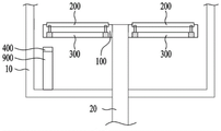
Fig. 9 is a schematic sectional view showing a substrate processing apparatus according to another embodiment. The tray 100 and the susceptor 200 may be disposed in a process chamber 10, the process chamber 10 including a reaction space. At this time, the disk 100, the susceptor 200, the metal ring 300, and the magnet 400 may be disposed in the process chamber 10.
The disc 100 may perform a first rotation, i.e. a rotation on its axis. For example, the disc 100 may perform a first rotation as the shaft 20 connected to the disc 100 rotates.
At least one susceptor 200 may be disposed on the tray 100 such that a substrate may be placed on an upper surface of the susceptor 200. As the disk 100 performs a first rotation, i.e., rotation on its axis, the susceptor 200 may perform not only the first rotation but also a second rotation, i.e., revolution around the center of the disk 100.
At this time, as described above, the rotation of the base 200 on its axis may be achieved using the magnetic force acting between the metal ring 300 and the magnet 400. Next, the configuration and arrangement relationship of the metal ring 300 and the magnet 400 will be described.
As shown in fig. 9, the metal ring 300 may be coupled to the outer circumferential surface of the susceptor 200, and the magnet 400 may be coupled to the inner wall of the process chamber 10 so as to be laterally opposite to the metal ring 300.
The disk 100 rotates on its axis as the shaft 20 rotates, and then the base 200 may revolve around the center of the disk 100 as the disk 100 rotates on its axis. At this time, the metal ring 300 connected to the susceptor 200 may revolve around the center of the disk 100, and a magnetic force may act between the metal ring 300 revolving around the center of the disk 100 and the magnet 400 connected to the inner wall of the process chamber 10 so as not to rotate.
Due to the magnetic force, the metal ring 300 may rotate on the center of the base 200, and the base 200 connected with the metal ring 300 may rotate on its axis.
Meanwhile, since the magnet 400 and the metal ring 300 are opposite to each other in the lateral direction, vibration and noise generated when the base 200 is rotated on its axis may be suppressed, as compared to the above-described configuration (i.e., the configuration in which the magnet 400 and the metal ring 300 are opposite to each other in the vertical direction).
Meanwhile, although a plurality of magnets 400 may be radially arranged on the inner wall of the process chamber 10 having a cylindrical shape, one or more magnets may be arranged in a specific region on the inner wall of the process chamber 10 in an arrangement different from the radial arrangement.
This is because the metal ring 300 and the susceptor 200 revolve around the center of the disk 100 as the disk 100 rotates on its axis, and thus the magnetic force of the magnet 400 disposed in a specific region on the inner wall of the process chamber 10 has an influence on the metal ring 300.
Fig. 10 is a schematic sectional view showing a substrate processing apparatus according to still another embodiment. The embodiment shown in fig. 10 is different from the substrate processing apparatus shown in fig. 1 to 7 in the arrangement of the magnet 400.
That is, one end of the magnet 400 may be supported by the support column 900, and the support column 900 is connected to the process chamber 10 so as to be disposed below the metal ring 300 to be opposite to the metal ring 300 in a vertical direction. That is, the magnet 400 may not be directly connected to the disk 100 or the base 200, but may be separated and spaced apart from the disk 100 or the base 200.
Meanwhile, although a plurality of magnets 400 may be arranged radially below the metal ring 300 and the disk 100, one or more magnets may be arranged in a specific region within the process chamber 10 in an arrangement different from the radial arrangement.
In the same manner as described above, since the metal ring 300 and the susceptor 200 revolve around the center of the disk 100 as the disk 100 rotates on its axis, the magnetic force of the magnet 400 located in a specific region within the process chamber 10 may have an influence on the metal ring 300.
In the embodiment of fig. 9 and 10, since the magnet 400 is separated and spaced apart from the disk 100 or the susceptor 200, the substrate processing apparatus may be relatively simply manufactured compared to the case where the magnet 400 is coupled to the disk 100.
In various embodiments, since the susceptor 200 can be rotated on its axis without a separate rotation apparatus using air or gas, the configuration of the substrate processing apparatus may be simplified and power consumption used in the substrate processing process may be reduced.
In addition, it is possible to significantly reduce the occurrence of defective products caused when foreign substances contained in air or gas are absorbed onto a substrate (e.g., a wafer) in the case of using a rotating apparatus using air or gas.
Further, by suppressing vibration or noise generated during rotation of the susceptor 200, vibration of the substrate placed on the upper surface of the susceptor 200, uneven deposition of a film on the substrate, and erosion of the film can be suppressed.
While various embodiments have been described above, various other embodiments are possible. The technical descriptions of the embodiments described above can be combined in many different ways, as long as they are not mutually exclusive, so that a new embodiment can be implemented.
Industrial applicability
According to the present invention, since the susceptor can be rotated on its axis without an additional susceptor rotating apparatus using air or gas, the configuration of the substrate processing apparatus can be simplified and power consumption used in the substrate processing can be reduced. Therefore, it has industrial applicability.
Claims (14)
1. A substrate processing apparatus, comprising:
a disk provided to be rotatable on an axis thereof;
at least one susceptor arranged on the disk such that a substrate is placed on an upper surface of the susceptor, the susceptor being configured to rotate on an axis thereof and revolve around a center of the disk as the disk rotates on the axis thereof;
a metal ring connected to a lower portion of the base, the metal ring being disposed such that a center thereof coincides with a center of the base;
a magnet disposed below the disc to be radially arranged based on a center of the disc, at least a portion of the magnet being opposite to the metal ring in a vertical direction; and
a frame having an accommodating portion for accommodating the tray,
wherein the magnet is radially arranged on the frame based on a center of the receiving portion so as not to rotate.
2. The substrate processing apparatus of claim 1, further comprising:
bearings disposed in contact with the disk and the base, respectively,
wherein as the disk rotates on its axis, the metal ring rotates on its axis by the magnetic force of the magnet, thereby rotating the base on its axis.
3. The substrate processing apparatus of claim 2, wherein the susceptor comprises a first support protruding from a lower surface thereof, the first support being coupled to the metal ring and configured to support the bearing.
4. The substrate processing apparatus of claim 3, wherein the metal ring comprises:
an inner ring connected with the first support part;
an outer ring connected with the inner ring; and
a ring connecting portion formed between the outer ring and the inner ring for connecting the outer ring and the inner ring to each other.
5. The substrate processing apparatus of claim 4, wherein the outer ring is vertically opposite the magnet and has a width greater than a width of the magnet.
6. The substrate processing apparatus of claim 4, wherein the outer ring is vertically opposite the magnet and includes a region opposite the magnet for covering the entire magnet in a vertical direction.
7. The substrate processing apparatus of claim 1, wherein the magnet comprises a plurality of segments radially arranged at fixed intervals.
8. The substrate processing apparatus of claim 7, wherein the segments are cylindrical in shape.
9. The substrate processing apparatus of claim 1, further comprising:
a shaft inserted into a through hole formed in a central region of the receiving portion for rotating the disk on an axis thereof; and
a disk support portion having a lower side connected with an upper end of the shaft and an upper side connected with the disk.
10. The substrate processing apparatus of claim 1, wherein a speed at which the susceptor rotates on its axis is proportional to a ratio of a diameter of the metal ring and a diameter of the magnet.
11. The substrate processing apparatus according to claim 10, wherein the diameter of the magnet is a value obtained by measuring a distance in a diameter direction between opposite points on a width center of magnets arranged in a ring shape, and the diameter of the metal ring is a value obtained by measuring a distance in a diameter direction between opposite points on a width center of the metal ring.
12. The substrate processing apparatus of claim 1, wherein the metal ring is made of a ferromagnetic material.
13. The substrate processing apparatus of claim 1, wherein a direction in which the disk rotates on its axis is the same as a direction in which the susceptor rotates on the axis.
14. The substrate processing apparatus of claim 1, wherein the magnets disposed below the disk to be radially arranged based on a center of the disk have centers spaced apart from a center of the metal ring.
Priority Applications (1)
| Application Number | Priority Date | Filing Date | Title |
|---|---|---|---|
| CN202111132309.2A CN114005783A (en) | 2015-05-11 | 2016-05-10 | Substrate processing apparatus disposed in a process chamber and method of operating the same |
Applications Claiming Priority (5)
| Application Number | Priority Date | Filing Date | Title |
|---|---|---|---|
| KR10-2015-0065094 | 2015-05-11 | ||
| KR20150065094 | 2015-05-11 | ||
| KR10-2015-0097515 | 2015-07-09 | ||
| KR1020150097515A KR102508025B1 (en) | 2015-05-11 | 2015-07-09 | Substrate disposition apparatus arranged in process chamber and operating method thereof |
| PCT/KR2016/004842 WO2016182299A1 (en) | 2015-05-11 | 2016-05-10 | Substrate treatment device arranged inside process chamber and method for operating same |
Related Child Applications (1)
| Application Number | Title | Priority Date | Filing Date |
|---|---|---|---|
| CN202111132309.2A Division CN114005783A (en) | 2015-05-11 | 2016-05-10 | Substrate processing apparatus disposed in a process chamber and method of operating the same |
Publications (2)
| Publication Number | Publication Date |
|---|---|
| CN107667421A CN107667421A (en) | 2018-02-06 |
| CN107667421B true CN107667421B (en) | 2021-10-01 |
Family
ID=57537945
Family Applications (2)
| Application Number | Title | Priority Date | Filing Date |
|---|---|---|---|
| CN201680027285.5A Active CN107667421B (en) | 2015-05-11 | 2016-05-10 | Substrate processing apparatus disposed in a process chamber and method of operating the same |
| CN202111132309.2A Pending CN114005783A (en) | 2015-05-11 | 2016-05-10 | Substrate processing apparatus disposed in a process chamber and method of operating the same |
Family Applications After (1)
| Application Number | Title | Priority Date | Filing Date |
|---|---|---|---|
| CN202111132309.2A Pending CN114005783A (en) | 2015-05-11 | 2016-05-10 | Substrate processing apparatus disposed in a process chamber and method of operating the same |
Country Status (5)
| Country | Link |
|---|---|
| US (2) | US10229849B2 (en) |
| JP (1) | JP6959696B2 (en) |
| KR (1) | KR102508025B1 (en) |
| CN (2) | CN107667421B (en) |
| TW (1) | TWI702670B (en) |
Families Citing this family (3)
| Publication number | Priority date | Publication date | Assignee | Title |
|---|---|---|---|---|
| KR102508025B1 (en) * | 2015-05-11 | 2023-03-10 | 주성엔지니어링(주) | Substrate disposition apparatus arranged in process chamber and operating method thereof |
| KR20190140373A (en) * | 2018-06-11 | 2019-12-19 | 캐논 톡키 가부시키가이샤 | Substrate rotation apparatus, substrate rotation method and manufacturing method of electronic device |
| CN110643949B (en) * | 2019-10-29 | 2022-08-05 | 苏州华楷微电子有限公司 | Evaporation method of revolution type semiconductor evaporation table |
Citations (5)
| Publication number | Priority date | Publication date | Assignee | Title |
|---|---|---|---|---|
| JP2009206288A (en) * | 2008-02-27 | 2009-09-10 | Mtc:Kk | Thin substrate rotation processing equipment |
| KR101053047B1 (en) * | 2008-05-06 | 2011-08-01 | 삼성엘이디 주식회사 | Chemical vapor deposition apparatus |
| KR20130061802A (en) * | 2011-12-02 | 2013-06-12 | 주식회사 케이씨텍 | Deposition apparatus equipped with a rotating susceptor pocket |
| CN103322996A (en) * | 2013-06-20 | 2013-09-25 | 上海交通大学 | Electromagnetic-drive electrostatic-detection bulk acoustic wave harmonic-vibration triaxial microgyroscope and preparation method thereof |
| CN103597577A (en) * | 2011-06-01 | 2014-02-19 | 朗姆研究公司 | Device for treating surfaces of wafer-shaped articles |
Family Cites Families (13)
| Publication number | Priority date | Publication date | Assignee | Title |
|---|---|---|---|---|
| JPH01184277A (en) * | 1988-01-18 | 1989-07-21 | Matsushita Electric Ind Co Ltd | Substrate rotating device |
| US5795448A (en) * | 1995-12-08 | 1998-08-18 | Sony Corporation | Magnetic device for rotating a substrate |
| JP4470680B2 (en) * | 2004-10-12 | 2010-06-02 | 日立電線株式会社 | Vapor growth equipment |
| KR101200372B1 (en) * | 2005-06-15 | 2012-11-12 | 주성엔지니어링(주) | Thin film manufacturing apparatus and thin film deposition method using the same |
| KR100957525B1 (en) | 2008-01-18 | 2010-05-11 | 이석태 | Power device |
| JP5276388B2 (en) * | 2008-09-04 | 2013-08-28 | 東京エレクトロン株式会社 | Film forming apparatus and substrate processing apparatus |
| KR20100046962A (en) * | 2008-10-28 | 2010-05-07 | 세메스 주식회사 | Apparatus for conveying glass substrate |
| KR20110116901A (en) | 2010-04-20 | 2011-10-26 | 엘아이지에이디피 주식회사 | Apparatus for rotating suscepter and apparatus for chemical vapor deposition using the same |
| JP6017817B2 (en) * | 2011-12-15 | 2016-11-02 | 住友化学株式会社 | Surface treatment apparatus, surface treatment method, substrate support mechanism, and program |
| JP6050944B2 (en) * | 2012-04-05 | 2016-12-21 | 東京エレクトロン株式会社 | Plasma etching method and plasma processing apparatus |
| JP6330630B2 (en) * | 2014-11-13 | 2018-05-30 | 東京エレクトロン株式会社 | Deposition equipment |
| KR102508025B1 (en) * | 2015-05-11 | 2023-03-10 | 주성엔지니어링(주) | Substrate disposition apparatus arranged in process chamber and operating method thereof |
| JP6507953B2 (en) * | 2015-09-08 | 2019-05-08 | 東京エレクトロン株式会社 | Substrate processing apparatus and substrate processing method |
-
2015
- 2015-07-09 KR KR1020150097515A patent/KR102508025B1/en active IP Right Grant
-
2016
- 2016-05-10 CN CN201680027285.5A patent/CN107667421B/en active Active
- 2016-05-10 US US15/573,480 patent/US10229849B2/en active Active
- 2016-05-10 JP JP2017559429A patent/JP6959696B2/en active Active
- 2016-05-10 CN CN202111132309.2A patent/CN114005783A/en active Pending
- 2016-05-11 TW TW105114563A patent/TWI702670B/en active
-
2019
- 2019-01-31 US US16/264,637 patent/US10818534B2/en active Active
Patent Citations (5)
| Publication number | Priority date | Publication date | Assignee | Title |
|---|---|---|---|---|
| JP2009206288A (en) * | 2008-02-27 | 2009-09-10 | Mtc:Kk | Thin substrate rotation processing equipment |
| KR101053047B1 (en) * | 2008-05-06 | 2011-08-01 | 삼성엘이디 주식회사 | Chemical vapor deposition apparatus |
| CN103597577A (en) * | 2011-06-01 | 2014-02-19 | 朗姆研究公司 | Device for treating surfaces of wafer-shaped articles |
| KR20130061802A (en) * | 2011-12-02 | 2013-06-12 | 주식회사 케이씨텍 | Deposition apparatus equipped with a rotating susceptor pocket |
| CN103322996A (en) * | 2013-06-20 | 2013-09-25 | 上海交通大学 | Electromagnetic-drive electrostatic-detection bulk acoustic wave harmonic-vibration triaxial microgyroscope and preparation method thereof |
Also Published As
| Publication number | Publication date |
|---|---|
| KR102508025B1 (en) | 2023-03-10 |
| JP6959696B2 (en) | 2021-11-05 |
| US20190164801A1 (en) | 2019-05-30 |
| JP2018515930A (en) | 2018-06-14 |
| TW201701390A (en) | 2017-01-01 |
| CN107667421A (en) | 2018-02-06 |
| KR20160132743A (en) | 2016-11-21 |
| US20180144968A1 (en) | 2018-05-24 |
| CN114005783A (en) | 2022-02-01 |
| TWI702670B (en) | 2020-08-21 |
| US10229849B2 (en) | 2019-03-12 |
| US10818534B2 (en) | 2020-10-27 |
Similar Documents
| Publication | Publication Date | Title |
|---|---|---|
| US10584416B2 (en) | Substrate processing apparatus | |
| CN107667421B (en) | Substrate processing apparatus disposed in a process chamber and method of operating the same | |
| US20220415692A1 (en) | Substrate Processing Apparatus and Rotating Electrical Connector for Vacuum | |
| KR20170092105A (en) | Substrate processing apparatus | |
| CN109643641B (en) | Substrate processing apparatus | |
| KR102399075B1 (en) | Substrate producing apparatus arranged in process chamber | |
| KR20170027641A (en) | Substrate disposition apparatus and operating method thereof | |
| CN110214405A (en) | Motor | |
| US10517146B2 (en) | Internal chamber rotation motor, alternative rotation | |
| KR102408889B1 (en) | Substrate Processing Apparatus | |
| JP2018515930A5 (en) | ||
| KR101136536B1 (en) | Coating appratus usisng magnetic | |
| JP2002093767A (en) | Single wafer cleaning equipment | |
| US20190362951A1 (en) | Pvd reactor with magnetic rotation mechanism | |
| EP1093157A2 (en) | Substrate processing method and apparatus | |
| KR100959725B1 (en) | Chemical vapor deposition apparatus | |
| KR102510956B1 (en) | Substrate disposition apparatus | |
| KR20160148157A (en) | Substrate disposition apparatus arranged in process chamber and operating method thereof | |
| JPH11274042A (en) | Wafer processing apparatus | |
| KR101321582B1 (en) | Susceptor having a function of self-balancing and deposition equipment using the same | |
| KR20110123670A (en) | Vertical plating equipment and plating method thereof | |
| JPH08288265A (en) | Microwave plasma etching system |
Legal Events
| Date | Code | Title | Description |
|---|---|---|---|
| PB01 | Publication | ||
| PB01 | Publication | ||
| SE01 | Entry into force of request for substantive examination | ||
| SE01 | Entry into force of request for substantive examination | ||
| GR01 | Patent grant | ||
| GR01 | Patent grant |