CN107466159B - Molded circuit board of camera module and manufacturing equipment and manufacturing method thereof - Google Patents
Molded circuit board of camera module and manufacturing equipment and manufacturing method thereof Download PDFInfo
- Publication number
- CN107466159B CN107466159B CN201610394707.4A CN201610394707A CN107466159B CN 107466159 B CN107466159 B CN 107466159B CN 201610394707 A CN201610394707 A CN 201610394707A CN 107466159 B CN107466159 B CN 107466159B
- Authority
- CN
- China
- Prior art keywords
- molding
- circuit board
- base
- mold
- manufacturing apparatus
- Prior art date
- Legal status (The legal status is an assumption and is not a legal conclusion. Google has not performed a legal analysis and makes no representation as to the accuracy of the status listed.)
- Active
Links
- 238000004519 manufacturing process Methods 0.000 title claims abstract description 173
- 238000000465 moulding Methods 0.000 claims abstract description 403
- 239000007788 liquid Substances 0.000 claims abstract description 118
- 238000000034 method Methods 0.000 claims abstract description 95
- 230000003287 optical effect Effects 0.000 claims abstract description 85
- 230000008569 process Effects 0.000 claims abstract description 83
- 239000007787 solid Substances 0.000 claims abstract description 56
- 239000000463 material Substances 0.000 claims abstract description 34
- 238000006243 chemical reaction Methods 0.000 claims abstract description 7
- 239000012778 molding material Substances 0.000 claims description 232
- 239000000758 substrate Substances 0.000 claims description 45
- 238000010438 heat treatment Methods 0.000 claims description 44
- 238000003860 storage Methods 0.000 claims description 30
- 229920001187 thermosetting polymer Polymers 0.000 claims description 27
- 230000007246 mechanism Effects 0.000 claims description 24
- 238000002844 melting Methods 0.000 claims description 20
- 230000008018 melting Effects 0.000 claims description 20
- 238000003475 lamination Methods 0.000 claims description 15
- 239000012943 hotmelt Substances 0.000 claims description 12
- 230000000694 effects Effects 0.000 claims description 6
- 238000007493 shaping process Methods 0.000 claims description 4
- 238000004891 communication Methods 0.000 claims description 3
- 238000006073 displacement reaction Methods 0.000 claims description 2
- 238000011112 process operation Methods 0.000 claims description 2
- 238000012546 transfer Methods 0.000 claims description 2
- 238000001723 curing Methods 0.000 description 26
- 238000010030 laminating Methods 0.000 description 12
- 239000003292 glue Substances 0.000 description 9
- 238000011049 filling Methods 0.000 description 8
- 239000011344 liquid material Substances 0.000 description 8
- 230000009471 action Effects 0.000 description 7
- 238000010586 diagram Methods 0.000 description 7
- 238000005520 cutting process Methods 0.000 description 6
- 239000000047 product Substances 0.000 description 6
- 238000001816 cooling Methods 0.000 description 5
- 238000004806 packaging method and process Methods 0.000 description 4
- 238000003825 pressing Methods 0.000 description 4
- 239000004065 semiconductor Substances 0.000 description 4
- 239000003990 capacitor Substances 0.000 description 3
- 238000012858 packaging process Methods 0.000 description 3
- 238000007711 solidification Methods 0.000 description 3
- 230000008023 solidification Effects 0.000 description 3
- 230000015572 biosynthetic process Effects 0.000 description 2
- 238000011161 development Methods 0.000 description 2
- 239000000428 dust Substances 0.000 description 2
- 230000017525 heat dissipation Effects 0.000 description 2
- 238000003384 imaging method Methods 0.000 description 2
- 230000010365 information processing Effects 0.000 description 2
- 238000012986 modification Methods 0.000 description 2
- 230000004048 modification Effects 0.000 description 2
- 239000000843 powder Substances 0.000 description 2
- 239000002994 raw material Substances 0.000 description 2
- 239000011347 resin Substances 0.000 description 2
- 229920005989 resin Polymers 0.000 description 2
- 239000011265 semifinished product Substances 0.000 description 2
- 239000000853 adhesive Substances 0.000 description 1
- 238000004026 adhesive bonding Methods 0.000 description 1
- 230000001070 adhesive effect Effects 0.000 description 1
- 239000000919 ceramic Substances 0.000 description 1
- 239000011093 chipboard Substances 0.000 description 1
- 239000011248 coating agent Substances 0.000 description 1
- 238000000576 coating method Methods 0.000 description 1
- 239000013039 cover film Substances 0.000 description 1
- 238000009826 distribution Methods 0.000 description 1
- 230000009977 dual effect Effects 0.000 description 1
- 238000009713 electroplating Methods 0.000 description 1
- 238000001914 filtration Methods 0.000 description 1
- 239000012530 fluid Substances 0.000 description 1
- 238000013007 heat curing Methods 0.000 description 1
- 239000012535 impurity Substances 0.000 description 1
- 238000011068 loading method Methods 0.000 description 1
- 238000010309 melting process Methods 0.000 description 1
- 230000002093 peripheral effect Effects 0.000 description 1
- 238000004321 preservation Methods 0.000 description 1
- 238000012545 processing Methods 0.000 description 1
- 238000007789 sealing Methods 0.000 description 1
- 238000005476 soldering Methods 0.000 description 1
- 239000012815 thermoplastic material Substances 0.000 description 1
- 230000001131 transforming effect Effects 0.000 description 1
- 230000007704 transition Effects 0.000 description 1
Images


Classifications
-
- B—PERFORMING OPERATIONS; TRANSPORTING
- B29—WORKING OF PLASTICS; WORKING OF SUBSTANCES IN A PLASTIC STATE IN GENERAL
- B29C—SHAPING OR JOINING OF PLASTICS; SHAPING OF MATERIAL IN A PLASTIC STATE, NOT OTHERWISE PROVIDED FOR; AFTER-TREATMENT OF THE SHAPED PRODUCTS, e.g. REPAIRING
- B29C45/00—Injection moulding, i.e. forcing the required volume of moulding material through a nozzle into a closed mould; Apparatus therefor
- B29C45/17—Component parts, details or accessories; Auxiliary operations
- B29C45/76—Measuring, controlling or regulating
- B29C45/78—Measuring, controlling or regulating of temperature
-
- H—ELECTRICITY
- H05—ELECTRIC TECHNIQUES NOT OTHERWISE PROVIDED FOR
- H05K—PRINTED CIRCUITS; CASINGS OR CONSTRUCTIONAL DETAILS OF ELECTRIC APPARATUS; MANUFACTURE OF ASSEMBLAGES OF ELECTRICAL COMPONENTS
- H05K3/00—Apparatus or processes for manufacturing printed circuits
- H05K3/0011—Working of insulating substrates or insulating layers
- H05K3/0014—Shaping of the substrate, e.g. by moulding
-
- B—PERFORMING OPERATIONS; TRANSPORTING
- B29—WORKING OF PLASTICS; WORKING OF SUBSTANCES IN A PLASTIC STATE IN GENERAL
- B29C—SHAPING OR JOINING OF PLASTICS; SHAPING OF MATERIAL IN A PLASTIC STATE, NOT OTHERWISE PROVIDED FOR; AFTER-TREATMENT OF THE SHAPED PRODUCTS, e.g. REPAIRING
- B29C45/00—Injection moulding, i.e. forcing the required volume of moulding material through a nozzle into a closed mould; Apparatus therefor
- B29C45/02—Transfer moulding, i.e. transferring the required volume of moulding material by a plunger from a "shot" cavity into a mould cavity
-
- B—PERFORMING OPERATIONS; TRANSPORTING
- B29—WORKING OF PLASTICS; WORKING OF SUBSTANCES IN A PLASTIC STATE IN GENERAL
- B29C—SHAPING OR JOINING OF PLASTICS; SHAPING OF MATERIAL IN A PLASTIC STATE, NOT OTHERWISE PROVIDED FOR; AFTER-TREATMENT OF THE SHAPED PRODUCTS, e.g. REPAIRING
- B29C45/00—Injection moulding, i.e. forcing the required volume of moulding material through a nozzle into a closed mould; Apparatus therefor
- B29C45/14—Injection moulding, i.e. forcing the required volume of moulding material through a nozzle into a closed mould; Apparatus therefor incorporating preformed parts or layers, e.g. injection moulding around inserts or for coating articles
- B29C45/14639—Injection moulding, i.e. forcing the required volume of moulding material through a nozzle into a closed mould; Apparatus therefor incorporating preformed parts or layers, e.g. injection moulding around inserts or for coating articles for obtaining an insulating effect, e.g. for electrical components
- B29C45/14655—Injection moulding, i.e. forcing the required volume of moulding material through a nozzle into a closed mould; Apparatus therefor incorporating preformed parts or layers, e.g. injection moulding around inserts or for coating articles for obtaining an insulating effect, e.g. for electrical components connected to or mounted on a carrier, e.g. lead frame
-
- B—PERFORMING OPERATIONS; TRANSPORTING
- B29—WORKING OF PLASTICS; WORKING OF SUBSTANCES IN A PLASTIC STATE IN GENERAL
- B29C—SHAPING OR JOINING OF PLASTICS; SHAPING OF MATERIAL IN A PLASTIC STATE, NOT OTHERWISE PROVIDED FOR; AFTER-TREATMENT OF THE SHAPED PRODUCTS, e.g. REPAIRING
- B29C45/00—Injection moulding, i.e. forcing the required volume of moulding material through a nozzle into a closed mould; Apparatus therefor
- B29C45/17—Component parts, details or accessories; Auxiliary operations
- B29C45/26—Moulds
- B29C45/27—Sprue channels ; Runner channels or runner nozzles
-
- B—PERFORMING OPERATIONS; TRANSPORTING
- B29—WORKING OF PLASTICS; WORKING OF SUBSTANCES IN A PLASTIC STATE IN GENERAL
- B29C—SHAPING OR JOINING OF PLASTICS; SHAPING OF MATERIAL IN A PLASTIC STATE, NOT OTHERWISE PROVIDED FOR; AFTER-TREATMENT OF THE SHAPED PRODUCTS, e.g. REPAIRING
- B29C45/00—Injection moulding, i.e. forcing the required volume of moulding material through a nozzle into a closed mould; Apparatus therefor
- B29C45/17—Component parts, details or accessories; Auxiliary operations
- B29C45/64—Mould opening, closing or clamping devices
-
- H—ELECTRICITY
- H04—ELECTRIC COMMUNICATION TECHNIQUE
- H04N—PICTORIAL COMMUNICATION, e.g. TELEVISION
- H04N23/00—Cameras or camera modules comprising electronic image sensors; Control thereof
-
- H—ELECTRICITY
- H04—ELECTRIC COMMUNICATION TECHNIQUE
- H04N—PICTORIAL COMMUNICATION, e.g. TELEVISION
- H04N23/00—Cameras or camera modules comprising electronic image sensors; Control thereof
- H04N23/50—Constructional details
-
- H—ELECTRICITY
- H04—ELECTRIC COMMUNICATION TECHNIQUE
- H04N—PICTORIAL COMMUNICATION, e.g. TELEVISION
- H04N23/00—Cameras or camera modules comprising electronic image sensors; Control thereof
- H04N23/50—Constructional details
- H04N23/54—Mounting of pick-up tubes, electronic image sensors, deviation or focusing coils
-
- H—ELECTRICITY
- H04—ELECTRIC COMMUNICATION TECHNIQUE
- H04N—PICTORIAL COMMUNICATION, e.g. TELEVISION
- H04N23/00—Cameras or camera modules comprising electronic image sensors; Control thereof
- H04N23/57—Mechanical or electrical details of cameras or camera modules specially adapted for being embedded in other devices
-
- H—ELECTRICITY
- H05—ELECTRIC TECHNIQUES NOT OTHERWISE PROVIDED FOR
- H05K—PRINTED CIRCUITS; CASINGS OR CONSTRUCTIONAL DETAILS OF ELECTRIC APPARATUS; MANUFACTURE OF ASSEMBLAGES OF ELECTRICAL COMPONENTS
- H05K3/00—Apparatus or processes for manufacturing printed circuits
-
- H—ELECTRICITY
- H05—ELECTRIC TECHNIQUES NOT OTHERWISE PROVIDED FOR
- H05K—PRINTED CIRCUITS; CASINGS OR CONSTRUCTIONAL DETAILS OF ELECTRIC APPARATUS; MANUFACTURE OF ASSEMBLAGES OF ELECTRICAL COMPONENTS
- H05K3/00—Apparatus or processes for manufacturing printed circuits
- H05K3/22—Secondary treatment of printed circuits
- H05K3/28—Applying non-metallic protective coatings
- H05K3/284—Applying non-metallic protective coatings for encapsulating mounted components
-
- B—PERFORMING OPERATIONS; TRANSPORTING
- B29—WORKING OF PLASTICS; WORKING OF SUBSTANCES IN A PLASTIC STATE IN GENERAL
- B29C—SHAPING OR JOINING OF PLASTICS; SHAPING OF MATERIAL IN A PLASTIC STATE, NOT OTHERWISE PROVIDED FOR; AFTER-TREATMENT OF THE SHAPED PRODUCTS, e.g. REPAIRING
- B29C45/00—Injection moulding, i.e. forcing the required volume of moulding material through a nozzle into a closed mould; Apparatus therefor
- B29C45/14—Injection moulding, i.e. forcing the required volume of moulding material through a nozzle into a closed mould; Apparatus therefor incorporating preformed parts or layers, e.g. injection moulding around inserts or for coating articles
- B29C45/14639—Injection moulding, i.e. forcing the required volume of moulding material through a nozzle into a closed mould; Apparatus therefor incorporating preformed parts or layers, e.g. injection moulding around inserts or for coating articles for obtaining an insulating effect, e.g. for electrical components
- B29C45/14655—Injection moulding, i.e. forcing the required volume of moulding material through a nozzle into a closed mould; Apparatus therefor incorporating preformed parts or layers, e.g. injection moulding around inserts or for coating articles for obtaining an insulating effect, e.g. for electrical components connected to or mounted on a carrier, e.g. lead frame
- B29C2045/14663—Injection moulding, i.e. forcing the required volume of moulding material through a nozzle into a closed mould; Apparatus therefor incorporating preformed parts or layers, e.g. injection moulding around inserts or for coating articles for obtaining an insulating effect, e.g. for electrical components connected to or mounted on a carrier, e.g. lead frame the mould cavity walls being lined with a film, e.g. release film
-
- B—PERFORMING OPERATIONS; TRANSPORTING
- B29—WORKING OF PLASTICS; WORKING OF SUBSTANCES IN A PLASTIC STATE IN GENERAL
- B29C—SHAPING OR JOINING OF PLASTICS; SHAPING OF MATERIAL IN A PLASTIC STATE, NOT OTHERWISE PROVIDED FOR; AFTER-TREATMENT OF THE SHAPED PRODUCTS, e.g. REPAIRING
- B29C45/00—Injection moulding, i.e. forcing the required volume of moulding material through a nozzle into a closed mould; Apparatus therefor
- B29C45/16—Making multilayered or multicoloured articles
- B29C45/1671—Making multilayered or multicoloured articles with an insert
- B29C2045/1673—Making multilayered or multicoloured articles with an insert injecting the first layer, then feeding the insert, then injecting the second layer
-
- B—PERFORMING OPERATIONS; TRANSPORTING
- B29—WORKING OF PLASTICS; WORKING OF SUBSTANCES IN A PLASTIC STATE IN GENERAL
- B29C—SHAPING OR JOINING OF PLASTICS; SHAPING OF MATERIAL IN A PLASTIC STATE, NOT OTHERWISE PROVIDED FOR; AFTER-TREATMENT OF THE SHAPED PRODUCTS, e.g. REPAIRING
- B29C2945/00—Indexing scheme relating to injection moulding, i.e. forcing the required volume of moulding material through a nozzle into a closed mould
- B29C2945/76—Measuring, controlling or regulating
- B29C2945/76494—Controlled parameter
- B29C2945/76531—Temperature
-
- B—PERFORMING OPERATIONS; TRANSPORTING
- B29—WORKING OF PLASTICS; WORKING OF SUBSTANCES IN A PLASTIC STATE IN GENERAL
- B29C—SHAPING OR JOINING OF PLASTICS; SHAPING OF MATERIAL IN A PLASTIC STATE, NOT OTHERWISE PROVIDED FOR; AFTER-TREATMENT OF THE SHAPED PRODUCTS, e.g. REPAIRING
- B29C2945/00—Indexing scheme relating to injection moulding, i.e. forcing the required volume of moulding material through a nozzle into a closed mould
- B29C2945/76—Measuring, controlling or regulating
- B29C2945/76655—Location of control
- B29C2945/76732—Mould
-
- B—PERFORMING OPERATIONS; TRANSPORTING
- B29—WORKING OF PLASTICS; WORKING OF SUBSTANCES IN A PLASTIC STATE IN GENERAL
- B29C—SHAPING OR JOINING OF PLASTICS; SHAPING OF MATERIAL IN A PLASTIC STATE, NOT OTHERWISE PROVIDED FOR; AFTER-TREATMENT OF THE SHAPED PRODUCTS, e.g. REPAIRING
- B29C45/00—Injection moulding, i.e. forcing the required volume of moulding material through a nozzle into a closed mould; Apparatus therefor
- B29C45/16—Making multilayered or multicoloured articles
- B29C45/1671—Making multilayered or multicoloured articles with an insert
-
- B—PERFORMING OPERATIONS; TRANSPORTING
- B29—WORKING OF PLASTICS; WORKING OF SUBSTANCES IN A PLASTIC STATE IN GENERAL
- B29L—INDEXING SCHEME ASSOCIATED WITH SUBCLASS B29C, RELATING TO PARTICULAR ARTICLES
- B29L2031/00—Other particular articles
- B29L2031/34—Electrical apparatus, e.g. sparking plugs or parts thereof
-
- H—ELECTRICITY
- H05—ELECTRIC TECHNIQUES NOT OTHERWISE PROVIDED FOR
- H05K—PRINTED CIRCUITS; CASINGS OR CONSTRUCTIONAL DETAILS OF ELECTRIC APPARATUS; MANUFACTURE OF ASSEMBLAGES OF ELECTRICAL COMPONENTS
- H05K2201/00—Indexing scheme relating to printed circuits covered by H05K1/00
- H05K2201/10—Details of components or other objects attached to or integrated in a printed circuit board
- H05K2201/10007—Types of components
- H05K2201/10121—Optical component, e.g. opto-electronic component
-
- H—ELECTRICITY
- H05—ELECTRIC TECHNIQUES NOT OTHERWISE PROVIDED FOR
- H05K—PRINTED CIRCUITS; CASINGS OR CONSTRUCTIONAL DETAILS OF ELECTRIC APPARATUS; MANUFACTURE OF ASSEMBLAGES OF ELECTRICAL COMPONENTS
- H05K2201/00—Indexing scheme relating to printed circuits covered by H05K1/00
- H05K2201/10—Details of components or other objects attached to or integrated in a printed circuit board
- H05K2201/10007—Types of components
- H05K2201/10151—Sensor
-
- H—ELECTRICITY
- H05—ELECTRIC TECHNIQUES NOT OTHERWISE PROVIDED FOR
- H05K—PRINTED CIRCUITS; CASINGS OR CONSTRUCTIONAL DETAILS OF ELECTRIC APPARATUS; MANUFACTURE OF ASSEMBLAGES OF ELECTRICAL COMPONENTS
- H05K2203/00—Indexing scheme relating to apparatus or processes for manufacturing printed circuits covered by H05K3/00
- H05K2203/13—Moulding and encapsulation; Deposition techniques; Protective layers
- H05K2203/1305—Moulding and encapsulation
- H05K2203/1316—Moulded encapsulation of mounted components
Abstract
A mould circuit board of camera module group and its manufacturing equipment and method, wherein the manufacturing equipment includes a forming mould, which includes a first mould and a second mould capable of opening and closing mould, wherein the first and second moulds form a forming cavity when closing mould, and a light window forming block and a base forming guide groove around the light window forming block are arranged in the forming cavity, wherein, when the circuit board is installed in the forming cavity, the mould material filled into the base forming guide groove is solidified and formed through the conversion process from liquid state to solid state, a mould base is formed at the position corresponding to the base forming guide groove, a through hole of the mould base is formed at the position corresponding to the light window forming block, wherein the mould base is integrally formed on the circuit board to form the mould circuit board of camera module group. The through hole is used for providing an optical path for the camera module, and the molding base can be used as a bracket of the camera module.
Description
Technical Field
The present invention relates to a circuit board of a camera module, and more particularly, to a molded circuit board of a camera module, and a manufacturing apparatus and a manufacturing method thereof.
Background
Along with the development of various electronic products and intelligent equipment, the camera module is also developing towards higher performance and light and thin direction, and in the face of the development requirements of various high performances such as high pixel and high imaging quality, electronic components in the circuit are more and more, the area of the chip is larger and more, and passive components such as driving resistor and capacitor are correspondingly increased, so that the specification of the electronic components is larger and larger, the assembly difficulty is increased continuously, and the integral size of the camera module is larger and larger.
The conventional camera module generally includes a circuit board, a photosensitive element, a lens holder, a lens, and other components, and the package of the camera module generally adopts a cob (chip On board) process, wherein the photosensitive element is connected to the circuit board, and the lens holder is attached to the circuit board through glue.
In addition, the lens base or the motor is adhered to the circuit board through an adhesive such as glue, and a calibration process is usually performed during adhesion, namely, central axes of the photosensitive element and the lens are adjusted to be consistent in a horizontal direction and a vertical direction. The mirror base can not be smoothly attached to the circuit board by using glue for bonding.
In addition, in the process of attaching and packaging, the electronic components and the photosensitive element of the circuit board are exposed in the environment, so that dirt and dust which are easy to adhere to the electronic components of the circuit board or even further reach the photosensitive element are inevitable, and the assembled camera module has bad phenomena such as dirty and black spots and the like, and the product yield is reduced.
The above problems can be solved by integrally packaging and molding the mirror base on the circuit board, but there is no such circuit board with integrally packaged and molded mirror base in the prior art, and there is no suitable packaging device. In a conventional semiconductor integrated package molding process, a liquid material is generally packaged on a whole semiconductor substrate, and the liquid material can cover the whole semiconductor material in a large area, and then the liquid material is cured to complete the package.
However, the circuit board of the camera module and the lens holder structure thereof are limited, and the conventional semiconductor packaging process has not been applied to the manufacture of such a circuit board with an integrally packaged lens holder. On the one hand, the camera module has higher requirements on size, precision and flatness. On the other hand, the circuit board needs to be matched with the photosensitive element, the lens holder is generally annular, an optical window needs to be arranged in the middle of the lens holder so as to facilitate the optical alignment of the photosensitive element and the lens and enable light passing through the lens to reach the photosensitive element through the optical window, and the bottom side of the lens holder needs to be tightly and seamlessly combined with the circuit board. On the other hand, the circuit board of the camera module usually has a plurality of electronic components, such as resistors, capacitors, drivers, etc., and the integrated packaging process needs to reasonably arrange the electronic components, and the molding structure of the molding mold is designed to be only capable of forming the lens base with the optical window at the peripheral position of the circuit board, but not capable of entering the effective photosensitive area of the circuit board and the photosensitive element to influence the photosensitive effect. In addition, the forming mold is also required to be designed to match the size of the circuit board, such as area, thickness, etc., so as to form the lens holder with a suitable size.
Disclosure of Invention
The invention aims to provide a molded circuit board of a camera module, manufacturing equipment and a manufacturing method thereof, wherein the molded circuit board comprises a molded base and a circuit board, and the molded base can integrally mold raw materials for forming the molded base on the circuit board through the manufacturing equipment so as to enable the molded circuit board to form an integral packaging structure.
Another object of the present invention is to provide a molded circuit board of a camera module, and a manufacturing apparatus and a manufacturing method thereof, wherein a photosensitive element of the camera module can also be formed into an integral structure with the molded circuit board through a molding process, i.e., the mold base can be integrally formed on the circuit board and the photosensitive element, thereby further forming an integral compact structure.
Another object of the present invention is to provide a molded circuit board of a camera module, and a manufacturing apparatus and a manufacturing method thereof, wherein the molded circuit board does not require glue to be attached during the integral molding process of the mold base, so that the molded circuit board has better flatness and smaller thickness, and the camera module is conveniently calibrated, and is lighter and thinner and has better performance.
Another object of the present invention is to provide a molded circuit board of a camera module, and a manufacturing apparatus and a manufacturing method thereof, wherein the manufacturing apparatus enables the mold base to be integrally formed with the circuit board, so that the integrally and tightly bonded structure enables the mold base to block stray light, enhance a heat dissipation function of the circuit board, and enhance the strength of the molded circuit board.
Another object of the present invention is to provide a molded circuit board of a camera module, and a manufacturing apparatus and a manufacturing method thereof, in which the molded base integrally covers a plurality of electronic components of the circuit board so that the electronic components are not directly exposed to the external environment.
Another object of the present invention is to provide a molded circuit board of a camera module, a manufacturing apparatus and a manufacturing method thereof, wherein a plurality of electronic components of the circuit board are arranged at an edge region of a substrate thereof, and a molding die of the manufacturing apparatus is prevented from entering a liquid molding material corresponding to a central die lamination region of the circuit board, so that the liquid material is coated at the edge region of an outer side of the circuit board to form the molding base for coating the electronic components.
Another object of the present invention is to provide a molded circuit board of a camera module, a manufacturing apparatus and a manufacturing method thereof, wherein the manufacturing apparatus has the molding die capable of manufacturing the molded circuit board, and in a molding step, a central chip-overlapping region of the circuit board is made to correspond to the optical window molding block of the molding die by at least one optical window molding block and at least one base molding guide groove provided in a molding cavity thereof, so as to prevent a liquid material from entering, and the base molding guide groove around the optical window molding block is filled with the liquid material to form the molding base.
Another object of the present invention is to provide a molded circuit board of a camera module, and a manufacturing apparatus and a manufacturing method thereof, wherein the molding mold further prevents liquid material from entering through one or more motor pin hole forming portions during mold closing, so that the molded base forms corresponding motor pin holes after curing, so as to facilitate attaching the pins of the motor to the circuit board during manufacturing of the moving-focus camera module.
Another object of the present invention is to provide a molded circuit board of a camera module, a manufacturing apparatus and a manufacturing method thereof, in which the molding step is performed after the molding dies of the manufacturing apparatus are closed by first and second dies, in which the circuit board is fixed in the molding cavity of the molding die set, and then the liquid material forming the mold base can enter the base molding guide groove in the molding cavity and be cured to form the mold base.
Another object of the present invention is to provide a molded circuit board of a camera module, and a manufacturing apparatus and a manufacturing method thereof, in which the first and second molds are configured to be relatively displaceable to enable opening and closing of the molds, one of the molds is fixed and the other is movable, or both of the molds are movable, thereby facilitating the operation.
Another object of the present invention is to provide a molded circuit board of a camera module, a manufacturing apparatus and a manufacturing method thereof, in which a material forming the mold base may be a hot-melt material, so as to be injected into the molding cavity in a liquid state, and may be solidified and molded by cooling.
Another object of the present invention is to provide a molded circuit board of a camera module, a manufacturing apparatus and a manufacturing method thereof, in which a raw material forming the mold base may be a thermosetting material so as to be injected into the molding cavity in a liquid state and may be cured and molded by continuing heating.
Another object of the present invention is to provide a molded circuit board of a camera module, a manufacturing apparatus and a manufacturing method thereof, in which the circuit board can be preheated, so that the temperature difference between the circuit board and a liquid molding material can be reduced in a molding process.
Another object of the present invention is to provide a molded circuit board of a camera module, and a manufacturing apparatus and a manufacturing method thereof, wherein the manufacturing apparatus can manufacture a single molded circuit board, or the manufacturing apparatus is configured to manufacture a molded circuit board assembly, and the molded circuit board assembly is cut to form a plurality of molded circuit boards forming a single camera module or a plurality of molded circuit boards forming an array camera module.
Another object of the present invention is to provide a molded circuit board of a camera module, and a manufacturing apparatus and a manufacturing method thereof, wherein when the molding mold is closed, the liquid molding material enters the base molding guide groove under pressure, so that it can be formed on the circuit board in a flat manner, and the flat molding surface of the molding mold can ensure that the top surface and the side surface of the molded base are also formed with better flatness.
Another object of the present invention is to provide a molded circuit board of a camera module, and a manufacturing apparatus and a manufacturing method thereof, in which the liquid molding material introduced into the base forming guide groove can be precisely controlled, thereby ensuring formation of the molded base of an appropriate size.
To achieve the above object, the present invention provides a manufacturing apparatus for manufacturing at least one molded circuit board of at least one camera module, wherein the manufacturing apparatus comprises:
a forming die, which comprises a first die and a second die;
a mold fixing device capable of separating or closing the first and second molds, wherein the first and second molds form at least one molding cavity when closed, and the molding mold is provided with at least one optical window molding block and a base molding guide groove around the optical window molding block in the molding cavity; and
and the temperature control device is used for providing a temperature control environment for the forming cavity, when at least one circuit board is installed in the forming cavity, a molding material filled into the base forming guide groove undergoes a liquid-to-solid conversion process under the temperature control action of the temperature control device and is solidified and formed, a molding base is formed at the position corresponding to the base forming guide groove, a through hole of the molding base is formed at the position corresponding to the optical window forming block, and the molding base is integrally formed on the circuit board to form the molding circuit board of the camera module. It will be appreciated that the optical window is adapted to provide an optical path for the camera module, and the molded base may serve as a support for the camera module.
In some embodiments, the first and second molds are capable of relative displacement to effect opening and closing of the mold, wherein at least one of the first and second molds is configured to be movable.
In some embodiments, the light window forming block and the base forming guide groove are disposed in the first mold, and the second mold has at least one circuit board positioning groove for mounting the circuit board.
In some embodiments, the light window forming block and the base forming guide groove are disposed in the second mold, and the first mold has at least one circuit board positioning groove for mounting the circuit board.
In some embodiments, the first mold is a stationary upper mold and the second mold is a movable lower mold.
In some embodiments, the light window forming block and the base forming channel are integrally formed with the first mold.
In some embodiments, the molding structure providing the light window molding block and the base molding guide groove is detachably disposed on the first mold so as to be suitable to be replaced to manufacture the molded circuit board with different specifications.
In some embodiments, the manufacturing apparatus further comprises a molding material supply mechanism having at least one reservoir, at least one feed channel, and at least one pusher, wherein the molding material is filled from the reservoir via the feed channel into the base-forming channel via the pusher.
In some embodiments, the reservoir is provided with a heated environment such that the molding material in the solid state in the reservoir is heated to melt and pushed into the feed channel.
In some embodiments, the molding material in the solid state in the storage tank is pushed into the feeding channel by the pusher while being heated and melted.
In some embodiments, the molding material in a solid state in the storage tank is heated and melted into a pure liquid, and then is pushed into the feeding channel by the pusher.
In some embodiments, the mold fixture of the manufacturing apparatus is configured to drive at least one of the first and second molds to move so as to position the first and second molds coaxially spaced apart or closely together.
In some embodiments, the manufacturing apparatus further comprises a vacuum apparatus for evacuating the molding cavity.
In some embodiments, the temperature control device includes a melting heating device for melting the molding material in a solid state and a solidifying temperature control device for providing a heating environment for the forming mold; or the temperature control device is an integrated temperature control device and can be used for heating and melting the molding material in a solid state and heating the molding material in the forming cavity to thermoset and form the molding material in a liquid state.
In some embodiments, the manufacturing apparatus further comprises a circuit board panel feeding mechanism for supplying at least one circuit board panel to the molding die, wherein the circuit board panels are integrally joined to a plurality of the circuit boards, the circuit board panel feeding mechanism comprises at least one guide rail, at least one loader and at least one unloader, and the loader and the unloader move along the guide rail to transfer the circuit board before molding to the molding cavity and unload the molded circuit board after molding from the molding cavity, respectively.
In some embodiments, the manufacturing apparatus further comprises a controller for automating the molding process operations of the manufacturing apparatus.
In some embodiments, at least one circuit board panel is mounted in the molding cavity, the circuit board panel comprises a plurality of integrally joined circuit boards, and the manufacturing equipment is used for obtaining at least one molded circuit board panel through panel molding operation of the circuit board panel, wherein the molded circuit board panel comprises a plurality of integrally joined molded circuit boards.
In some embodiments, each of the molded circuit boards has the molded base independent of the other.
In some embodiments, the molded circuit board has a molded base panel integrally formed with the circuit board panel.
In some embodiments, the molding material is a hot melt material, and is filled into the base forming guide groove to form a liquid molten state, and after being cooled and solidified, the molding material forms the molding base integrally formed on the circuit board.
In some embodiments, the molding material is a thermosetting material, and is filled into the base forming guide groove to be in a liquid molten state, and is thermally cured to form the molding base integrally formed on the circuit board.
In some embodiments, the circuit board includes a substrate and a plurality of electronic components disposed on the substrate, wherein the molded base integrally covers the electronic components.
In some embodiments, the substrate has a central chip stacking region and an edge region around the chip stacking region, wherein the electronic component is disposed at the edge region.
In some embodiments, the chip lamination area provides a flat bonding surface to closely fit with the bottom surface of the light window forming block to prevent the molding material in liquid form from entering the chip lamination area.
In some embodiments, the chip lamination area and the edge area of the substrate are in the same plane.
In some embodiments, the chip stacking region of the substrate is recessed relative to the edge region so that the substrate forms an inner groove, the bottom end of the optical window forming block protrudes out of the base forming guide groove, and the forming mold closes and performs a molding process, the bottom end of the optical window forming block extends into the inner groove, and the inner groove is used for assembling a photosensitive element of the camera module.
In some embodiments, the molding die is further provided with a side guide groove communicated with the base molding guide groove and located on at least one side of the circuit board when the molding die is closed to perform the molding process, and the molding material in a liquid state is filled into the side guide groove, so that the molding base formed after the curing molding is further coated on the side of the circuit board.
In some embodiments, the molding die is further provided with a bottom side guide groove communicated with the base molding guide groove and located on at least a part of the bottom surface of the circuit board when the molding die is closed to perform the molding process, and the molding material in a liquid state is filled into the bottom side guide groove so that the molding base formed after the curing molding further covers the at least a part of the bottom surface of the circuit board.
In some embodiments, the circuit board further has one or more through holes extending in a thickness direction thereof, wherein when the forming mold is closed to perform a molding process, the molding material in a liquid state further fills into the through holes and is cured and formed in the through holes.
In some embodiments, the circuit board to be molded is further connected with at least one photosensitive element, wherein the molding base is integrally formed on the circuit board and the photosensitive element.
In some embodiments, the circuit board to be molded and the photosensitive element are electrically connected through one or more leads.
In some embodiments, the photosensitive element has a photosensitive region and a non-photosensitive region located around the photosensitive region, wherein when the forming mold is closed to perform a molding process, the optical window forming block is tightly attached to the photosensitive region, and the molding base is integrally formed in at least a portion of the non-photosensitive region after curing.
In some embodiments, the molded base integrally encapsulates the leads and the electronic components of the circuit board.
In some embodiments, the circuit board to be molded further has at least one photosensitive element and an optical filter stacked on the photosensitive element, wherein when the molding mold is closed to perform a molding process, the optical window molding block is tightly attached to a central region of the optical filter, so that the molding base and the molding base are integrally formed on the circuit board, the photosensitive element and the optical filter after curing.
In some embodiments, the forming mold is further provided with one or more motor pin slot forming blocks extending in the base forming guide groove when the mold is closed, and a motor pin slot is formed at a position corresponding to the motor pin slot forming block after a molding material filled into the base forming guide groove is solidified and formed through a liquid-to-solid conversion process.
In some embodiments, the light window shaping block is shaped and dimensioned to match the desired shape and dimensions of the light window, and the base shaping channel is shaped and dimensioned to match the desired shape and dimensions of the molded base.
In some embodiments, the light window forming block further comprises a forming part body and a stepped part of the top end integrally formed with the forming part body to form a groove at the top side of the formed molding base.
According to another aspect of the present invention, there is provided a method for manufacturing a molded circuit board of a camera module, comprising the steps of:
(a) fixing at least one circuit board to a second mold of a molding mold;
(b) after the second mold and a first mold are closed, filling a liquid molding material into at least one base molding guide groove in the molding mold, wherein the position corresponding to at least one optical window molding block is prevented from being filled with the molding material, and the base molding guide groove is positioned around the optical window molding block;
And
(c) and the molding material in the base forming guide groove is changed from a liquid state to a solid state, so that a molding base is formed at a position corresponding to the base forming guide groove, and an optical window of the molding base is formed at a position corresponding to the optical window forming block, wherein the molding base is integrally formed on the circuit board to form the molding circuit board of the camera module.
According to some embodiments of the present invention, wherein in step (a) at least one circuit board panel is secured to the second mold, wherein the circuit board panel comprises a plurality of the circuit boards integrally connected, and in step (b) the molding material is filled into a base panel molding guide groove having a plurality of the base molding guide grooves in communication, the circuit board panel being integrally molded with a molded base panel after the curing step of step (c) to provide a molded circuit board panel.
According to some embodiments of the invention, the method of manufacturing further comprises the steps of: and cutting the jointed board of the molded circuit board to obtain a plurality of molded circuit boards.
According to some embodiments of the invention, the method of manufacturing further comprises the steps of: attaching a photosensitive element to the circuit board, and then fixing the circuit board attached with the photosensitive element to the second mold, so that the integrally molded molding base is further molded on at least a part of the non-photosensitive area of the photosensitive element after the curing step of the step (c).
According to some embodiments of the invention, the method of manufacturing further comprises the steps of: respectively connecting a plurality of photosensitive elements to each circuit board of the circuit board jointed boards, and then fixing the circuit board jointed boards connected with the photosensitive elements to the second mold, so that after the curing step of the step (c), the integrally-formed molding base jointed board is further formed on at least one part of the non-photosensitive area of the photosensitive elements.
According to some embodiments of the invention, wherein in step (b) further comprises the step of: at least one of the first and second molds is driven to move by a mold fixing device to be clamped with the first and second molds to form at least one closed molding cavity.
According to some embodiments of the invention, further comprising the step of: before the step (b), further comprising the steps of: preheating the circuit board to reduce the temperature difference between the circuit board and the molding material when performing the step (b).
According to some embodiments of the invention, the method of manufacturing further comprises the steps of: automatically conveying the circuit board jointed boards to the forming mold through at least one loader moving along at least one guide rail; and after step (c), automatically transporting the molded circuit board panel to a storage location by moving at least one unloader along the guide rail.
According to some embodiments of the invention, before the step (b), the method further comprises the steps of: after the solid molding material is fed into at least one storage tank and heated to melt to a pure liquid, the molding material in liquid form is pushed into one or more feed channels communicating with the storage tank by at least one pusher, and the molding material in liquid form enters the base forming channel via the feed channels.
According to some embodiments of the invention, before the step (b), further comprising the steps of: feeding the solid molding material into at least one storage tank, and in the process of melting, pushing the gradually melted molding material into one or more feeding channels communicated with the storage tank under the action of at least one pusher, wherein the liquid molding material enters the base forming guide groove through the feeding channels.
According to some embodiments of the invention, wherein the molding material is a hot melt material, in the step (c), further comprising the steps of: cooling the liquid molding material to solidify and form the molding base.
According to some embodiments of the invention, wherein the molding material is a thermosetting material, wherein in the step (c), further comprising the steps of: heating the molding material in a liquid state so that the molding material is thermally cured to form the molding base.
According to some embodiments of the invention, the method of manufacturing further comprises the steps of: and replacing a molding structure detachably arranged on the first mold and used for providing the optical window molding block and the base molding guide groove with another molding structure of different specifications suitable for manufacturing the molded circuit board of different specifications.
According to another aspect of the present invention, there is provided a molded circuit board of a camera module, wherein the molded circuit board is manufactured by the following manufacturing method:
(a) fixing at least one circuit board to a second mold of a molding mold;
(b) after the second mold and a first mold are closed, filling a liquid molding material into at least one base molding guide groove in the molding mold, wherein the position corresponding to at least one optical window molding block is prevented from being filled with the molding material, and the base molding guide groove is positioned around the optical window molding block;
and
(c) and the molding material in the base forming guide groove is changed from a liquid state to a solid state, so that a molding base is formed at a position corresponding to the base forming guide groove, and an optical window of the molding base is formed at a position corresponding to the optical window forming block, wherein the molding base is integrally formed on the circuit board to form the molding circuit board of the camera module.
In some embodiments, wherein in said step (a) at least one circuit board panel is secured to said second mold, wherein said circuit board panel comprises a plurality of said circuit boards integrally joined, and in said step (b) said molding material is filled into at least one base panel forming channel having a plurality of said base forming channels in communication, said circuit board panel being integrally formed with a molded base panel after said curing of step (c) to provide a molded circuit board panel, said molded circuit board panel further being cut to provide a plurality of said molded circuit boards.
According to another aspect of the present invention, there is provided a forming mold for manufacturing at least one molded circuit board of at least one camera module, comprising a first mold and a second mold capable of being separated or combined, wherein the first and second molds form at least one forming cavity when combined, and the forming mold is configured with at least one optical window forming block and a base forming guide groove around the optical window forming block in the forming cavity, wherein when at least one circuit board is installed in the forming cavity, a molding material filled into the base forming guide groove undergoes a liquid-to-solid conversion process under the temperature control of the temperature control device to be cured and formed, a molding base is formed at a position corresponding to the base forming guide groove, and an optical window of the molding base is formed at a position corresponding to the optical window forming block, wherein the molding base is integrally formed on the circuit board to form the molding circuit board of the camera module.
Drawings
Fig. 1 is a block diagram configuration diagram of a manufacturing apparatus of a molded circuit board according to a preferred embodiment of the present invention.
Fig. 2A is a schematic cross-sectional view of a molding die of the manufacturing apparatus of the molded circuit board according to the above preferred embodiment of the present invention when the die is opened.
Fig. 2B is a schematic sectional view of the molding die of the manufacturing apparatus of the molded circuit board according to the above preferred embodiment of the present invention when the dies are closed.
Fig. 3A is a schematic perspective view of a first mold of the molding molds of the manufacturing apparatus of the molded circuit board according to the above preferred embodiment of the present invention.
Fig. 3B is a partially enlarged structural view of the optical window forming block and the base forming guide groove of the first mold of the forming mold of the manufacturing apparatus of the molded circuit board according to the above preferred embodiment of the present invention.
Fig. 4 is a perspective view of a second mold of the molding mold of the manufacturing apparatus of the molded circuit board according to the above preferred embodiment of the present invention.
Fig. 5 is a schematic perspective view of the circuit board when it is placed in the second mold of the molding mold of the manufacturing apparatus for molding a circuit board according to the above preferred embodiment of the present invention.
Fig. 6 is a sectional view showing a position where a circuit board and a molding material are disposed in the molding die of the manufacturing apparatus of the molded circuit board according to the above preferred embodiment of the present invention, wherein the sectional view is a sectional view taken along the line B-B shown in fig. 5.
Fig. 7 is a sectional view showing the time when the circuit board and the resin material are fixed in place in the molding die of the manufacturing apparatus of the molded circuit board according to the above-described preferred embodiment of the present invention, wherein the sectional view is a sectional view taken along the line B-B shown in fig. 5.
Fig. 8 is a sectional view showing a state where a liquid molding material is pushed into a base molding guide groove in the molding die of the manufacturing apparatus of the molded circuit board according to the above preferred embodiment of the present invention, wherein the sectional view is a sectional view taken along the line B-B shown in fig. 5.
Fig. 9A is a sectional view taken along line B-B in fig. 5 illustrating a molding step performed in the molding die of the manufacturing apparatus of the molded circuit board according to the above preferred embodiment of the present invention to form a mold base.
Fig. 9B is a sectional view taken along line C-C in fig. 5 illustrating a molding step performed in the molding die of the manufacturing apparatus of the molded circuit board according to the above preferred embodiment of the present invention to form a mold base.
Fig. 10 is a schematic perspective view of the molded circuit board manufactured by the molding process according to the above embodiment of the invention.
Fig. 11 is a sectional view taken along line D-D of the molded circuit board manufactured by the molding process according to the above-described embodiment of the present invention.
Fig. 12 is a sectional view of a camera module assembled by the molded circuit board manufactured by the molding process according to the above embodiment of the present invention.
Fig. 13 is an exploded perspective view of a camera module assembled by the molded circuit board manufactured by the molding process according to the above embodiment of the invention.
Fig. 14 is a cross-sectional view of the molded circuit board according to a variant of the above-described embodiment of the invention.
Fig. 15A is a sectional view of the molded circuit board according to the above-described modified embodiment of the above-described embodiment of the present invention before the molding dies are clamped and molded.
Fig. 15B is a sectional view of the molded circuit board according to the above-described modified embodiment of the above-described embodiment of the present invention after the molding dies are clamped and molded.
Fig. 16A is a cross-sectional view of the molded circuit board according to another modified embodiment of the above-described embodiment of the present invention.
Fig. 16B is a sectional view of the molded circuit board according to the above-described another modified embodiment of the above-described embodiment of the present invention, before the molding dies are closed and molded.
Fig. 16C is a sectional view of the molded circuit board according to the above-described another modified embodiment of the above-described embodiment of the present invention after the molding dies are closed and molded.
Fig. 17 is a sectional view of the molded circuit board according to another modified embodiment of the above-described embodiment of the present invention.
Fig. 18 is a sectional view of the molded circuit board according to the above-described another modified embodiment of the above-described embodiment of the present invention before the molding dies are closed and molded.
Fig. 19 is a sectional view of the molded circuit board according to the above-described another modified embodiment of the above-described embodiment of the present invention after the molding dies are clamped and molded.
Fig. 20 is a sectional view of the molded circuit board according to another modified embodiment of the above-described embodiment of the present invention after the molding dies are closed and molded.
Fig. 21 is a flow chart illustrating the method for manufacturing the molded circuit board according to the above embodiment of the present invention.
Fig. 22 is a schematic block diagram of an apparatus for manufacturing a molded circuit board panel in accordance with another embodiment of the present invention.
Fig. 23 is a perspective view of the apparatus for manufacturing the molded circuit board panels according to another embodiment of the present invention.
Fig. 24A is a sectional view of the molding tool of the manufacturing apparatus for the molded circuit board panels according to the above another embodiment of the present invention, taken along the length thereof when the mold is opened.
Fig. 24B is a sectional view of the molding tool of the apparatus for manufacturing molded circuit board panels according to another preferred embodiment of the present invention taken along the length thereof when closed.
Fig. 25A is a cross-sectional view of the molding tool of the manufacturing apparatus for the molded circuit board panels according to the above another embodiment of the present invention, taken along the width direction thereof when the mold is opened.
Fig. 25B is a cross-sectional view of the molding tool of the apparatus for manufacturing boards assembled from molded circuit boards according to another preferred embodiment of the present invention taken along the width of the molding tool when the mold is closed.
Fig. 26A is a perspective view of a first mold of the molding mold of the apparatus for manufacturing molded circuit board panels according to another preferred embodiment of the present invention.
Fig. 26B is a perspective view of the light window forming block and base panel forming guide groove of the first mold of the molding mold of the apparatus for manufacturing molded circuit board panels according to another preferred embodiment of the present invention.
Fig. 27 is a perspective view of a second mold of the molding mold of the manufacturing device for the molded circuit board panels according to the above another preferred embodiment of the present invention.
Fig. 28 is a perspective view of the apparatus for manufacturing molded circuit board panels according to another preferred embodiment of the present invention when the circuit board panels are placed in the second mold of the molding mold.
Fig. 29 is a sectional view showing a position where a circuit board and a molding material are disposed in the molding die of the manufacturing apparatus for the molded circuit board assembly according to the above-mentioned another preferred embodiment of the present invention, wherein the sectional view is a sectional view taken along the length direction of the molding die.
Fig. 30 is a sectional view showing the manufacturing equipment of the molded circuit board panels according to the another preferred embodiment of the present invention, with the circuit board panels and the resin material fixed in place in the molding die, wherein the sectional view is a sectional view taken along the length direction of the molding die.
Fig. 31 is a sectional view showing the liquid molding material pushed into the base molding guide groove in the molding die of the apparatus for manufacturing the molded circuit board panels according to the another preferred embodiment of the present invention, wherein the sectional view is a sectional view taken along the length direction of the molding die.
Fig. 32A is a sectional view of the molded circuit board panel manufacturing apparatus performing a molding step in the molding die to form a molded base panel according to the above another preferred embodiment of the present invention, wherein the sectional view is a sectional view taken along the length of the molding die.
Fig. 32B is a sectional view showing a molding step performed in the molding die of the manufacturing apparatus for the molded circuit board panels according to the above-mentioned another preferred embodiment of the present invention to form molded base panels, wherein the sectional view is a sectional view taken along the width direction of the molding die to show a structure for forming motor pin grooves.
Fig. 33 is a perspective view of the molded circuit board panel made by the molding process according to another embodiment of the present invention.
Fig. 34 is a schematic structural diagram of a single molded circuit board obtained by cutting the molded circuit board panels manufactured by the molding process according to another embodiment of the invention.
Fig. 35 is a schematic structural diagram of a camera module made of a single molded circuit board obtained by cutting the molded circuit board panel made by the molding process according to another embodiment of the invention.
Fig. 36 is a schematic structural diagram of a molded circuit board manufactured by a molding process for manufacturing an array camera module according to a modified embodiment of the another embodiment of the present invention.
Fig. 37A is a schematic structural diagram of a molded circuit board panel for assembling the array camera module according to the molding process of the other embodiment of the invention.
Fig. 37B is an exploded perspective view of the array camera module assembled by the molded circuit board manufactured by the molding process according to another embodiment of the invention.
Fig. 38 is a cross-sectional view of the molded circuit board according to another modified implementation of another example of the above-described embodiment of the invention.
Fig. 39 is a cross-sectional view of the molded circuit board after the molding dies are closed and molded according to another modified embodiment of the above another embodiment of the above-described embodiment of the present invention.
FIG. 40 is a schematic flow chart of a molding process according to another embodiment of the present invention described above.
Detailed Description
The following description is provided to disclose the invention so as to enable any person skilled in the art to practice the invention. The preferred embodiments in the following description are given by way of example only, and other obvious variations will occur to those skilled in the art. The basic principles of the invention, as defined in the following description, may be applied to other embodiments, variations, modifications, equivalents, and other technical solutions without departing from the spirit and scope of the invention.
It will be understood by those skilled in the art that in the present disclosure, the terms "longitudinal," "lateral," "upper," "lower," "front," "rear," "left," "right," "vertical," "horizontal," "top," "bottom," "inner," "outer," and the like are used in an orientation or positional relationship indicated in the drawings for ease of description and simplicity of description, and do not indicate or imply that the referenced devices or components must be constructed and operated in a particular orientation and thus are not to be considered limiting.
It is understood that the terms "a" and "an" should be interpreted as meaning that a number of one element or element is one in one embodiment, while a number of other elements is one in another embodiment, and the terms "a" and "an" should not be interpreted as limiting the number.
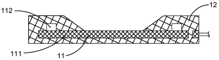
Fig. 1 to 13 show a molded circuit board 10 of a camera module 100 and a manufacturing apparatus 200 thereof according to a preferred embodiment of the present invention. As shown in fig. 10 to 13, the molded circuit board includes a circuit board 11 and a molded base 12, wherein the molded base 12 of the present invention is integrally formed on the circuit board 11 by the manufacturing apparatus 200, so that the molded base 12 can replace a lens holder or a bracket of a conventional camera module, and does not need to attach the lens holder or the bracket to a circuit board through glue like in a conventional packaging process.
The camera module 100 further includes a photosensitive element 20 and a lens 30. Wherein the mold base 12 includes a ring-shaped mold body 121 with a light window 122 in the middle to provide a light path for the lens 30 and the photosensitive element 20. The photosensitive element 20 is operatively connected to the circuit board 11, such as by COB wire bonding the photosensitive element 20 to the circuit board 11 on the top side of the circuit board 11, or by Flip Chip mounting the photosensitive element 20 on the bottom side of the circuit board 11. The photosensitive element 20 and the lens 30 are respectively assembled on two sides of the mold base 12 and are arranged in optical alignment, so that light passing through the mirror 30 can reach the photosensitive element through the optical window 122, and the image pickup module 100 can provide an optical image after photoelectric conversion.
The camera module 100 may be a fixed focus camera module or a moving focus camera module. As shown in fig. 12 and 13, the camera module 100 may be a moving focus camera module having a motor 40 (driver), and the lens 30 is mounted to the motor 40. The molded base 12 may be used to support the motor 40. The top side of the molded base 12 may also be provided with a filter 50 for filtering light passing through the lens 30, such as an infrared cut filter.
The circuit board 11 includes a substrate 111, and a plurality of electronic components 112 formed on the substrate 111, for example, mounted by SMT process, wherein the electronic components 112 include, but are not limited to, resistors, capacitors, driving devices, etc. In this embodiment of the present invention, the mold base 12 integrally covers the electronic component 112, so as to prevent dust and impurities from adhering to the electronic component 112 and further contaminating the photosensitive element 20, which affects the imaging effect, like in a conventional camera module. It is understood that in another modified embodiment, it is also possible that the electronic component 112 is buried in the substrate 111, i.e., the electronic component 112 may not be exposed. The substrate 111 of the circuit board 111 may be a hard PCB, a soft PCB, a rigid-flex board, a ceramic substrate, or the like. It should be noted that, in the preferred embodiment of the present invention, since the mold base 12 can completely cover the electronic components 112, the electronic components 112 may not be embedded in the substrate 111, and the substrate 111 is only used for forming the conductive traces, so that the final molded circuit board 10 can be made thinner.
In the preferred embodiment of the present invention, as shown in fig. 10 to 13, the substrate 111 includes a central lamination area 111a corresponding to the stacked photosensitive elements 20, an edge area 111b is formed around the central lamination area 111b, and the electronic component 112 can be disposed on the edge area 111b, so as to provide a relatively flat central lamination area 111a, so that the central lamination area 111a of the substrate 111 can be closely attached to a mold surface of the manufacturing apparatus to prevent the molding material 13 from entering the central lamination area 111a when molding is performed, as will be described in further detail below.
It can be understood that the molding base 12 of the present invention is fixed to the circuit board 11 by a molding process, without a bonding and fixing process, the molding method has better connection stability and controllability of the process compared to the bonding and fixing, and a glue space for calibration and adjustment is not required to be reserved between the molding base 12 and the circuit board 11, so that the thickness of the camera module is reduced; on the other hand, the molded base 12 covers the electronic component 112, so that a safety distance is not required to be reserved around the electronic component like a conventional camera module. In addition, the molding base 12 replaces a traditional lens base or a traditional bracket, so that the inclination error caused by the adhesion and assembly of the lens base or the bracket is avoided, and the accumulated tolerance of the camera module assembly is reduced. And the mold base 12 is integrally formed with the circuit board 11, so that the integrally tightly combined structure enables the mold base 12 to block stray light, enhances the heat dissipation function of the circuit board 11, and enhances the strength of the mold circuit board 11.
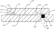
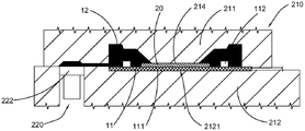
Further, as shown in fig. 1 to 9, the apparatus 200 for manufacturing the molded circuit board 10 of the camera module 100 includes a molding die 210, a molding material supply mechanism 220, a die fixing device 230, a temperature control device 250, and a controller 260, wherein the controller 260 is used for automatically controlling the molding material supply mechanism 220 during a molding process. The forming mold 210 includes a first mold 211 and a second mold 212 which can be opened and closed by the mold fixing device 230, that is, the mold fixing device 230 can separate and close the first mold 211 and the second mold 212 to form a forming cavity 213, when the molds are closed, the circuit board 11 is fixed in the forming cavity 213, and the liquid molding material 13 enters the forming cavity 213 to be integrally formed on the circuit board 11, and after being cured, the molding base 12 integrally formed on the circuit board 11 is formed.
More specifically, the molding module 210 further includes an optical window molding block 214 and a base molding guide groove 215 formed around the optical window molding block 214, when the first and second molds 211 and 212 are closed, the optical window molding block 214 and the base molding guide groove 215 are extended in the molding cavity 213, and the molding material 13 in a liquid state is filled into the base molding guide groove 215, and the molding material 13 in a liquid state cannot be filled at a position corresponding to the optical window molding block 214, so that the molding material 13 in a liquid state after being solidified at a position corresponding to the base molding guide groove 215 can form the annular molding body 121 of the molding base 12, and the optical window 122 of the molding base 12 is formed at a position corresponding to the optical window molding block 214.
The first and second molds 211 and 212 may be two molds capable of moving relatively, such as one of the two molds being fixed and the other being movable; or both molds may be movable, the invention is not limited in this respect. In the example of this embodiment of the invention, the first mold 211 is embodied in particular as a stationary upper mold, while the second mold 212 is embodied as a movable lower mold. The stationary upper mold and the movable lower mold are coaxially arranged, and as the movable lower mold is slidable in the upward direction along a plurality of positioning axes, the molding cavity 213 can be formed to be tightly closed when the upper mold is clamped.
The second mold 212, i.e., the lower mold, may have a circuit board positioning groove 2121 for mounting and fixing the circuit board 11, and the optical window forming block 214 and the base forming guide groove 215 may be formed at the first mold 211, i.e., the upper mold, to form the forming cavity 213 when the first and second molds 211 and 212 are closed. And the molding material 13 in a liquid state is injected into the base forming guide groove 215 of the top side of the circuit board 11, thereby forming the mold base 12 on the top side of the circuit board 11.
It is understood that the circuit board positioning groove 2121 may be provided in the first mold 211, i.e., the upper mold, for mounting and fixing the circuit board 11, and the optical window molding block 214 and the base molding guide groove 215 may be formed in the second mold 211 to form the molding cavity 213 when the first and second molds 211 and 212 are closed. The circuit board 11 may be arranged in the upper mold in a front-side orientation, and the molding material 13 in a liquid state is injected into the base forming guide groove 215 of the bottom side of the circuit board 11 which is inverted, thereby forming the molding base 12 on the bottom side of the circuit board 11 which is inverted.
More specifically, when the first and second molds 211 and 212 are closed and the molding step is performed, the light window molding block 214 is overlapped with the central die-overlapped region 111a of the substrate 111 of the circuit board 11, and the bottom surface of the light window molding block 214 is closely attached to the central die-overlapped region 111a of the substrate 111 of the circuit board 11, so that the molding material 13 in a liquid state is prevented from entering the central die-overlapped region 111a of the substrate 111 of the circuit board 11, thereby finally forming the light window 122 of the mold base 12 at a position corresponding to the light window molding block 214. The base forming guide groove 215 is located at the edge region 111b, so that when the base forming guide groove 215 is filled with the liquid molding material 13, the liquid molding material 13 is integrally bonded to the edge region 111b of the substrate 111 of the circuit board 11, and the molding base 12 can be formed outside the chip-on-chip region 111a in the center of the substrate 111 of the circuit board 11 after curing.
It is understood that, in this embodiment, the electronic component 112 of the circuit board 11 may be disposed outside the central die laminating area 111a, i.e. outside the position corresponding to the position where the photosensitive element 20 is mounted, so that the central die laminating area 111a is not provided with the electronic component 112 protruding, and thus the central die laminating area 111a of the substrate 111 of the circuit board 11 may provide a relatively flat surface, so that when the light window forming block 214 disposed on the first mold 211 is attached to the central die laminating area 111a of the substrate 111 of the circuit board 11, a gap is not formed between the bottom surface of the light window forming block 214 and the central die laminating area 111a of the substrate 111 of the circuit board 11 due to the protrusion, so that the liquid molding material 13 enters the central die laminating area 111a of the substrate 111 of the circuit board 11 during the molding process . That is, the bottom surface of the optical window molding block 214 can be closely attached to the top surface of the chip-overlapping region 111a in the center of the substrate 111 of the circuit board 11, so that the molding material 13 in a liquid state can reach only the periphery of the optical window molding block 214 to prevent the flash phenomenon. It can also be said that the chip laminating region 111a in the center of the substrate 111 of the circuit board 11 provides a bonding surface closely attached to the bottom surface of the light window molding block 214.
When the molding die 210 is closed, the electronic components 112 enter the base molding guide groove 215, and when the liquid molding material 13 enters the base molding guide groove 215, the liquid molding material 13 covers the surface of each electronic component 112,
it should be noted that the light window forming block 214 further includes a forming portion main body 2141 and a step portion 2142 formed integrally with the forming portion main body at the top end. The molded base 12 may thus also form a recess 123 at the top end of the light window 112, resulting in a stepped top surface of the molded base 12. Of course, in other embodiments, the molded base 12 may not have the above-mentioned recess 123 at the top end of the light window 112, but rather may form a flat top surface. The recess 123 formed in this embodiment of the present invention can be directly used for mounting the filter 50, that is, the stepped top surface on the inner side of the mold base 12 can be used for supporting the filter 50, and the stepped top surface on the outer side can be used for mounting the motor 40 or other components for supporting the lens 30, or directly used for supporting the lens 30. Or, a small bracket is further attached to the position of the groove 123, and the small bracket is used for mounting the optical filter 50. In addition, the shape of the light window 122 of the mold base 12 is not limited, and in the illustrated example, the light window 122 may have a square shape, and the light window forming block 214 may have a cylindrical structure, accordingly. In a further variant, this may be a frustum with a progressively larger diameter, for example.
It is understood that the molding surface of the first mold 211 forming the base molding guide 215 may be configured as a flat surface and be in the same plane, so that when the molding base 12 is cured, the top surface of the molding base 12 is flat, thereby providing a flat mounting condition for the motor 40, the lens 30 or other bearing components of the lens, and reducing the tilt error of the camera module 100 after assembly.
It should be noted that the base forming guide groove 215 and the light window forming block 214 may be integrally formed with the first mold 211. Alternatively, the first mold 211 further includes a detachable molding structure, and the molding structure is formed with the base molding guide groove 215 and the light window molding block 214. Thus, the base forming guide groove 215 and the light window forming block 214 may be designed in various shapes and sizes according to the shape and size requirements of the molded circuit board 10, such as the diameter and thickness of the molded base, and the like. In this way, only different molding structures need to be replaced, and the manufacturing equipment can be adapted to the molded circuit board 10 with different specification requirements. It will be appreciated that the second mold 212 may also include a removable mounting block to provide the recess 2121 with a different shape and size to facilitate replacement of the circuit board 11 to accommodate a different shape and size.
The molding material feeding mechanism 220 includes a hopper 221, a pusher 222, a melting and heating device 251, and has a feeding passage 223. The feed passage 223 communicates with the base forming guide 215. The hopper 221 has a storage vessel 2211, the molding material 13 can be placed in the storage vessel 2211, and the molding material 13 in a solid state is heated and melted by the melting and heating device 251 to become the molding material 13 in a liquid state. The hopper 221 may be a separate box or may be integrally formed with the second mold 212, that is, the hopper 2211 may be integrally formed at a partial position of the second mold 212. The feed channel 223 may be integrally formed in the molding material feed mechanism 220 or may be formed by a suitable feed conduit communicating with the storage slot 2211. in this preferred embodiment, the feed channel 223 is implemented as a guide slot formed in the bottom side of the first mold 211 or the second mold 212, such as the first mold 211, i.e., the upper mold, such that the feed channel 223 may form the feed channel 223 for feeding the molding material 13 to the base forming channel 215 when the first and second molds 211 and 212 are closed. It will be appreciated that upon completion of the molding process, a solidified extension formed from the molding material 13 will also be formed within the feed channel 223. After the molded product is removed, the feed passage 223 and the base molding guide groove 215 may be cleaned as needed. The pusher 222 may be a movable structure capable of pressing and pushing the molding material 13 in the storage tank 2211, such as a plunger. The melting and heating device 251 may be of any suitable structure capable of heating the molding material 13 in the solid state in the storage tank 2211, for example, a heating pipe filled with a heating fluid may be provided outside the storage tank 221.
It will be appreciated that the molding material 13 may also be weighed to accurately meter the liquid molding material 13 into the base forming channel 215. Alternatively, the molding material supply mechanism 220 may further include a quantitative distribution mechanism, such as a mechanism for calculating the amount of the molding material 13 in a liquid state filled into the base forming guide groove 215 by the flow rate of the molding material 13 and the diameter of the feed passage 223. Alternatively, the amount of the molding material 13 may be controlled by maintaining the pressure in the base forming channel 215 of the forming die 210. Of course, the quantitative control method is not limited to the above method, and other suitable methods may be used.
When the molding die 210 is in a closed state, the liquid molding material 13 is pushed through the feed channel 223 into the base molding guide groove 215 by the pushing and pressing action of the pusher 222, thereby filling the periphery of the optical window molding block 214. Finally, the liquid molding material 13 is subjected to a curing process to cure and harden the liquid molding material 13 located in the base forming guide groove 215 to form the molding base 12 integrally molded with the circuit board 11.
It is to be understood that the molding material 13 may be a hot-melt material such as a thermoplastic material, and the hot-melt material in a solid state is heated and melted by the melting and heating device to become the molding material 13 in a liquid state. During the molding process, the hot-melt molding material 13 is solidified and formed through a cooling process. The forming mold 210 may further be configured with a solidification temperature control device 252, which is used for providing a temperature control environment for the forming cavity 213, and cooling the molding material 13 in the liquid molten state in the base forming guide 215 so as to solidify and form the molding material 13 to form the molding base 12.
The molding material 13 may also be a thermosetting material, and the molding material 13 in a solid state and thermosetting is placed in the storage tank 2211. The thermosetting material in a solid state is heated and melted by the melting and heating device to melt the molding material 13 which becomes a liquid. During the molding, the thermosetting molding material 13 is cured by further heating and is no longer melted after being cured, thereby forming the molding base 12.
Accordingly, when the molding material 13 is a thermosetting material, the curing temperature control device 252 of the molding die 210 may be a curing heating device to continuously heat the liquid thermosetting molding material 13 entering the base molding guide 215, so as to thermoset the liquid thermosetting molding material 13. It is to be understood that the melting heating means for heating and melting the molding material 13 and the curing heating means for thermosetting the molding material 13 may be separate heating means or may be an integrated heating means. When using an integrated heating device, the melting temperature and the solidification holding temperature of the molding material 13 can be kept uniform, and at this time, it should be mentioned that the melting time in the storage tank 2211 needs to be controlled to avoid the solidification of the molding material 13 in the liquid state in the storage tank 2211. So that the molding material 13 in a solid state is pushed into the feed channel 223 by the pusher 222 when it is substantially completely melted into a liquid state. Alternatively, when the molding material 13 in a solid state starts to melt and is in a semi-solid state, the pusher 222 may start to push the molding material into the feeding passage 223 during the melting process. When different heating devices are used for melting and curing, the solid molding material 13 can be heated and melted to a liquid state in a relatively low temperature environment, and then fed into a higher temperature environment for curing and forming.
It is understood that the molding die 210 may preheat the circuit board 11 fixed in advance, for example, may be heated to a temperature during the curing process, so that the circuit board 11 and the liquid thermosetting molding material 13 do not have a great temperature difference during the molding process, thereby facilitating the liquid thermosetting molding material 13 to be closely bonded to the surface of the circuit board 11.
It is understood that, in this embodiment, the molding process of one circuit board 11 is illustrated, and in application, a plurality of independent circuit boards 11 may be molded simultaneously, that is, the molding material 13 in the storage tank 2211 is heated and melted, and then is conveyed to a plurality of independent circuit boards 11 through a plurality of the feeding channels 223 simultaneously to perform the molding process. Alternatively, the panel splicing work described in another embodiment below may be used.
Fig. 5 to 9B are schematic views illustrating a manufacturing process of the molded base 12 of the camera module 100 according to the preferred embodiment of the invention, wherein the sectional views of fig. 5 to 9A are taken along the line B-B as illustrated in fig. 5, and fig. 9B is taken along the line C-C as illustrated in fig. 5.
As shown in fig. 5 and 6, before the molding process, in this illustrative example, the circuit board 11 is fixed to the second mold 212, i.e., the lower mold, and the molding material 13 in a solid state may be disposed on one side of the circuit board 11.
As shown in fig. 7, the molding die 210 is in a clamped state, the circuit board 11 to be molded and the molding material 13 in a solid state are fixed in position, and the molding material 13 in a solid state is heated, thereby melting the molding material 13 in a liquid state. It is understood that in other examples, it is also possible that the molten molding material 13 is delivered into the holding tank 2211 through a conduit in a liquid or semi-solid state.
As shown in fig. 8, the melted molding material 13 enters the base forming guide 215 along the feeding passage 223 by the pusher 222 and reaches the periphery of the light window forming block 214. It is understood that the molding material 13 may be completely melted into a liquid state and then pushed into the feeding channel 223 by the pusher 222, or the molding material 13 may be pushed into the feeding channel 223 while being melted, and the molding material 13 in a solid state is completely melted into a liquid state by providing a heating environment by the forming mold 210.
As shown in fig. 9A and 9B, when the base forming guide groove 215 is completely filled with the liquid molding material 13, the liquid molding material 13 is cured and formed into the molding base 12 integrally formed on the circuit board 11 through a curing process. Taking the molding material 13 as a thermosetting material as an example, the molding material 13 that is heated and melted to be in a liquid state is further heated, so as to be cured and formed. For example, the temperature may be raised or the temperature may be kept for a predetermined time. For example, in the case of heat preservation and heat curing, in a specific example, the solid molding material 13 is heated in a heating environment at a predetermined temperature, such as 175C, for a first predetermined time to melt into a liquid state, and when being conveyed into the base forming guide slot 215, the solid molding material 13 is heated in the heating environment at the predetermined temperature for a second predetermined time to solidify and form the liquid molding material 13. It is to be understood that the temperature and the values of the first and second predetermined times are not provided as examples and do not limit the present invention. According to the material property of the molding material 13 and the requirement of the molding process, the material property can be adjusted according to the requirement in practical application. If the predetermined temperature is 110-250C, the melting heating time is 2-10 seconds, the curing heating time is 15 seconds-5 minutes, etc., the present invention is not limited in this respect to the values and value ranges in the above examples. In addition, after the molding process is completed, the molded circuit board 10 obtained may be taken out of the molding die 210 and continuously placed in a baking apparatus to be continuously heat-hardened for a predetermined time, such as 1 to 5 hours.
In addition, referring to fig. 21, the present invention provides a method for manufacturing a molded circuit board 10 of a camera module 100, which comprises the following steps:
fixing the circuit board 11: fixing the circuit board 11 in the molding die 210;
a step of filling the molding material 13: after the molding die 210 is closed, filling the liquid molding material 13 into the base molding guide groove 215 in the molding die 210, wherein the molding material 13 cannot be filled into the position of the light window molding block 214 of the molding die 210; and
a step of solidifying the molding material 13 in a liquid state: within the forming die 210, the molding material 13 within the base forming channel 215 transitions from a liquid state to a solid state.
It is to be understood that, in the step of fixing the circuit board 11, the forming mold 210 is in an open state, and the circuit board 11 may be fixed to the second mold 212 of the forming mold 210, or the circuit board 11 may be fixed to the first mold 211 of the forming mold 210. In this exemplary embodiment of the present invention, the circuit board 11 is fixed to the second mold 212, i.e., the lower mold 212, and the electronic component 112 of the circuit board 11 is located on the top side to be integrally covered by the molding material 13 in the subsequent molding step.
In the step of filling the molding material 13, according to this embodiment of the present invention, it further includes the steps of: the solid molding material 13 is fed into the storage tank 2211 in advance before the forming mold 210 is closed, and the solid molding material 13 may be solid blocks or solid powder; the solid molding material 13 is melted and conveyed into the base forming guide groove 215 through the feeding passage 223 by the pushing action of the pusher 222. After the pushing operation is completed, the molding material 13 in a liquid state fills the base forming guide groove 215.
A step of solidifying the molding material 13 in a liquid state: when the molding material 13 is a thermosetting material, the molding cavity 213 of the molding die 210 is provided with a heating environment, so that the liquid molding material 13 is thermosetting molded to form the molding base 12 integrally molded on the circuit board 11, and the molding base 12 covers the electronic component 112; when the molding material 13 is a hot melt material, the liquid molding material 13 is cooled in the molding die 210, and thereby cooled and solidified to form the mold base 12 integrally formed on the circuit board 11.
As shown in fig. 14, 15A and 15B, it is conceivable for those skilled in the art that, in another modified embodiment, the central die-laminating region 111a of the substrate 111 of the circuit board 11 may be recessed, that is, the central die-laminating region 111a and the edge region 111B of the substrate 111 of the circuit board 11 are not on the same surface, and the recessed die-laminating region 111a allows the top side of the substrate 111 of the circuit board 11 to form an inner groove 113, so that the optical window forming block 214 is protruded from the base forming guide groove 215, and the bottom end thereof extends into the inner groove 113 and is fitted into the recessed die-laminating region 111a, thereby further preventing the liquid molding material 13 from entering the inner groove 113 and reaching the die-laminating region 111 a. In addition, after such a circuit board 11 having the inner recess 113 is integrally molded with the mold base 12, the photosensitive element 20 may be mounted in the inner recess 113.
In addition, in the above example, after the mold base 12 is integrally formed on the circuit board 11 to obtain the molded circuit board 10, the photosensitive element 20 is assembled on the top side of the circuit board 11 of the molded circuit board 10 inside the mold base in a COB manner. In another modified embodiment, after the mold base 12 is formed and the circuit board 11 is formed with the opening, the photosensitive element 20 may be flip-chip mounted on the circuit board 11.
As shown in fig. 16A to 16C, according to a modified embodiment of the above-described embodiment of the present invention, in this modified embodiment of the present invention, the manufacturing mold 200 can manufacture the mold base 12 capable of covering not only the top surface of the circuit board 11. Specifically, at least one side surface and at least a part of the bottom surface of the mold base 12 may also be covered by the molding material 13, so as to enhance the strength of the molded circuit board 10 and facilitate the cutting of the molded circuit board 10 along the side surface covered side to obtain a finished product.
As shown in fig. 16B and 16C, when the molding die 210 is closed, at least one side surface of the circuit board 11 has a side guide groove 216, a bottom guide groove 217 is provided on the back surface of the circuit board 11, and the side guide groove 216 and the bottom guide groove 217 can communicate with the feeding passage 223. So that when the molding material 13 in a liquid state enters the molding die 210 through the feeding passage 223, it can fill the base molding guide groove 215 and the side guide groove 216 as well as the bottom side guide groove 217, so that the molding base 12 can further cover at least one side surface and at least a part of the bottom surface of the circuit board 11 after the curing step. It is understood that in alternative variations, rather than forming the annular base body 121, the molded base 12 may only cover at least one side of the circuit board 11, or only cover at least a portion of the bottom surface of the circuit board 11.
In addition, the substrate 111 of the circuit board 11 may further have one or more through holes 114, so that the liquid molding material 13 may further fill into the through holes 114 during the molding process to further enhance the strength of the formed molded integral structure. In this example, the through hole 114 may further connect the base forming channel 215 to the bottom side channel 217.
As shown in fig. 17 to 19, in another modified embodiment of the present invention, the manufacturing mold 200 may manufacture the molded circuit board 10 having the photosensitive element 20 capable of integrally encapsulating the photosensitive element 20. In this modified embodiment, the mold base 12 formed integrally covers the circuit board 11 and the photosensitive element 20 integrally.
More specifically, the photosensitive element 20 is connected to the circuit board 11 in advance, for example, electrically connected to the circuit board 11 by a cob (chip board) lead connection method. As shown in fig. 17, the photosensitive element 20 is connected to the circuit board 11 by one or more leads 21. The photosensitive element 20 has a photosensitive area 201 on the top surface and a non-photosensitive area 202 around the photosensitive area 201, i.e. the photosensitive area 201 is located at the center, and the non-photosensitive area 202 is located at the outer edge of the photosensitive element 20.
When the molding die 210 is opened, the circuit board 11 to which the photosensitive element 20 is connected is mounted on the second die 212. As shown in fig. 18 to 19, when the molding die 210 is clamped, the circuit board 11 to which the photosensitive element 20 is attached is located in the molding cavity 213 of the molding die 210. The light window forming block 214 is attached to the light sensing region 201 of the light sensing element 20, and the lead 21 and the electronic component 112 of the circuit board 11 are located in the base forming guide groove 215. Thus, when the liquid molding material 13 enters the forming mold 210 through the feeding channel 223, the liquid molding material 13 can only reach the periphery of the light window forming block 214, i.e. located in the base forming guide groove 215, i.e. the liquid molding material 13 is prevented from entering the photosensitive area 201 of the photosensitive element 20. Finally, outside the photosensitive region 201 of the photosensitive element 20, the liquid molding material 13 is cured to form the annular base body 121, i.e., the annular base body 121 is integrally formed on at least a portion of the non-photosensitive region 202 along the annular outer edge of the photosensitive element 20.
It can be understood that the molding base 12 is fixed to the circuit board 11 and the photosensitive element 20 through a molding process, a pasting and fixing process is not required, the molding manner has better connection stability and controllability of the process compared with the pasting and fixing, and a glue space for calibration and adjustment is not required to be reserved between the molding base 12 and the circuit board 11, so that the thickness of the camera module is reduced; on the other hand, the molding base 12 covers the electronic component 112 and the lead 21, and it is not necessary to reserve an operation space for connecting the photosensitive element 20 to the circuit board 11 by a subsequent wire bonding operation when the molding base 12 is only formed on the circuit board 11 as in the above embodiment, so that in this embodiment, the molding base 12 extends to the non-photosensitive region 202 of the photosensitive element 20, so that the molding base 12 can contract inward, thereby further reducing the transverse length and width dimensions of the camera module 100.
In another modified embodiment, after the light receiving element 20 is assembled on the circuit board 11, the optical filter 50 may be further stacked on the light receiving element 20, and then an integrated light receiving structure assembly formed by assembling the light receiving element 20 and the circuit board 11 on which the optical filter 50 is stacked may be mounted on the molding die 210, and when the molding die 210 is closed, the optical window molding block 214 may be attached to a central region of the optical filter 50 to prevent the molding material from entering a central region of the optical filter 50, and the liquid molding material 13 entering the base molding guide groove 215 may be integrally molded on edge regions of the circuit board 11 and the optical filter 50 after being cured to cover the electronic components 112 of the circuit board 11, thereby allowing the circuit board 11 to be molded via the mold base 12, the light sensing element 20 and the filter 50 form an integrally packaged compact structure.
As shown in fig. 20, according to the above-described further modified embodiment of fig. 17 to 19 of the present invention, a cover film 2111 is further attached to the first mold 211, i.e., the upper mold, of the molding mold 210, so that when the first and second molds 211 and 212 of the molding mold 210 are closed, the sealing property between the molding mold and the circuit board 11 and the photosensitive element 20 to be molded is enhanced, and the mold is released after the molding process is finished.
It is understood that in another variant embodiment, the molding surface of the first mold 211 of the molding mold 210 may be formed with an additional layer by electroplating or other suitable method to improve the performance of the molding surface, such as increasing the hardness, or selecting suitable materials to prevent scratches on the circuit board 11 and the photosensitive element 20.
Fig. 22 to 35 show the molded circuit board 10 of the camera module 100 and the manufacturing apparatus 200 thereof according to another embodiment of the present invention. The manufacturing equipment 200 can simultaneously manufacture the integrally combined molded circuit board panel 1000, the molded circuit board panel 1000 can be used as a semi-finished product, and then the semi-finished product can be cut as required to obtain a plurality of single finished products of the molded circuit board 10.
More specifically, as shown in fig. 22 and 23, the manufacturing apparatus includes a molding die 210, a molding material feeding mechanism 220, a die fixing device 230, a circuit board panel feeding mechanism 240, a temperature control device 250, and a controller 260. The molding mold 210 includes a first mold 211 and a second mold 212 capable of opening and closing the mold, the mold fixing device 230 is used for opening or closing the first and second molds 211 and 212, the molding material supply mechanism 220 is used for supplying the molding material 13 into the molding mold 210, the circuit board panel supply mechanism 240 is used for automatically supplying one or more circuit board panels 1100 to the molding mold 210, and the controller 260 is used for controlling the operation of the manufacturing apparatus.
More specifically, the mold 210 forms a mold cavity 213 when closed, and provides a plurality of optical window molding blocks 214 and one or more base panel molding guides 2150 having a plurality of base molding guides 215, the base molding guides 215 communicating and forming an integral guide.
It should be noted that the base panel forming guide 2150 and the optical window forming block 214 may be integrally formed with the first mold 211. Alternatively, the first mold 211 further comprises a detachable molding structure 219, and the molding structure 219 is formed with the base panel molding guide 2150 and the optical window molding block 214. Thus, different shapes and sizes of the base panel forming guide 2150 and the light window forming block 214 can be designed according to the shape and size requirements of different molded circuit board panels, such as the diameter and thickness of the formed unitary molded base, etc. Thus, only different molding structures 219 need be replaced to adapt the manufacturing equipment for use in making different specifications for the molded circuit board panel 1000. It will be appreciated that the second mold 212 may also include a removable retaining block to provide the recesses 2121 of different shapes and sizes to facilitate replacement of the circuit board panels 1100 to accommodate different shapes and sizes.
Similarly, the first mold 211 and the second mold 212 can be driven by the mold fixture 230 to move relatively, for example, one of the molds can be fixed while the other mold can be driven by the mold fixture 230 to move; or both molds may be moved by the mold fixture 230. In this embodiment of the present invention, the first mold 211 is implemented as a fixed upper mold, the second mold 212 is implemented as a movable lower mold, the mold fixing device 230 is used for driving the second mold 212 to move vertically, that is, the mold fixing device 230 can drive the second mold 212 to move upwards to cooperate with the first mold 211 to form the forming mold 210 in a closed state, and after the feeding or molding process is required to be finished, the mold fixing device 230 can drive the second mold 212 to move downwards to leave the first mold 211.
It will be appreciated by those skilled in the art that the mold fixture 230 may be any suitable device capable of driving the second mold 212 to move, for example, in one specific example, the mold fixture 230 may be implemented as a press device, which is driven by a power source such as an electric motor, hydraulic pressure, pneumatic pressure, etc. to push the second mold 212 to move upward and closely fit with the first mold 211 to form the relatively closed molding cavity 213. When it is necessary to leave the mold clamping operation, the press apparatus drives the second mold 212 downward by a reverse driving force, so that the first and second molds 211 and 212 are separated from each other.
It should be noted that, in this embodiment of the present invention, the example in which the first and second molds 211 and 212 are arranged in the vertical direction and the second mold 212 is driven to move upward or downward is only an example and is not a limitation of the present invention, and in another modified embodiment, the first and second molds 211 and 212 may be configured to be engaged in the horizontal direction or other directions.
The molding material feeding mechanism 220 includes one or more hoppers 221, one or more pushers 222, and has one or more feeding channels 223, for example, two feeding channels 223 may be arranged to supply the molding material 13 to two circuit board panels 1100. One or more material conveying mechanisms 224, which can convey a plurality of molding materials 13 in the form of material blocks to the corresponding hoppers 221 as required, may be further included.
The circuit board panel feeding mechanism 240 includes one or more feeding rails 241, a loader 242 supported on the feeding rails 241, and an unloader 243. Wherein under the control of the controller 260, one or more circuit board panels 1100 stored in a circuit board panel magazine are automatically transported by the loader 242 to the corresponding work station along each of the feeding rails 241. After the molding process is completed and the molded circuit board panel 1000 is cut, the molded circuit board panel 1000 may be unloaded by the unloader 243 and moved on the guide rails 241 to transport the molded circuit board panel 1000 into a product storage box.
It is understood that the mold fixture 230, the molding material feeding mechanism 220, the circuit board panel feeding mechanism 240 and the temperature control device 250 can be operated automatically and continuously under the control of the controller 260, so as to realize a continuous and automatic molding process. In addition, in some embodiments, the manufacturing apparatus 200 may further include a vacuum apparatus 270 for decompressing the molding cavity 213, exhausting air in the molding cavity 213, and pressing the first and second molds 211 and 212 more tightly.
Furthermore, a plurality of the feeding channels 223 are respectively communicated with the base jigsaw forming guide grooves 2150. Each of the hoppers 221 has a storage slot 2211, the molding material 13 can be placed in each storage slot 2211, and the molding material 13 in a solid state is heated and melted by the temperature control device 250 to become the liquid molding material 13. The hopper 221 may be a separate box or may be integrally formed with the second mold 212, that is, the storage slot 2211 may be integrally formed at a partial position of the second mold 212.
Of course, the manufacturing facility 200 may also provide a plurality of the stockers 221 and a corresponding plurality of the pushers 222 for performing the pushing operation, each of which may be independently operated to perform the molding operation on a plurality of the circuit board panels 1100. For example, in the example shown in fig. 23, the molding die 210 provides four processing stations that can simultaneously mold four of the circuit board panels 1100.
It can be understood that in the process of attaching the lens base of the traditional circuit board through the glue pasting process, the glue application amount is difficult to control, the smooth attachment cannot be ensured, the operation is long in time consumption, and the large-scale operation cannot be simultaneously carried out. When the molding process is used for production in a plate splicing mode, the manufacturing efficiency of the molded circuit board 10 is greatly improved.
Like the above-described embodiment, each of the feeding passages 223 may be integrally formed in the molding material supply mechanism 220, and in this preferred embodiment, the feeding passages 223 are implemented as guide grooves formed at the bottom side of the first mold 211, i.e., the upper mold. Each pusher 222 may be a movable structure capable of pressurizing and pushing the molding material 13 in the storage tank 2211, such as a plunger.
It will be appreciated that the molding material 13 may also be weighed, or the molding material 13 may be precisely metered by controlling the flow rate of the molding material 13, or the pressure within the forming mold and the accumulator, or other suitable means.
When the forming mold 210 is in a mold closing state, the liquid molding material 13 is pushed through the feeding channels 223 into the base panel forming guide 2150 by the pushing and pressing action of the ejectors 222, so as to fill the periphery of the light window forming blocks 214. Finally, the liquid molding material 13 is subjected to a curing process to cure and harden the liquid molding material 13 located in the base panel forming guide 2150 to form the molding bases 12 integrally molded on the circuit boards 11 of the circuit board panels 1100, and these molding bases 12 form the integrated molding base panel 1200. It is understood that the plurality of circuit boards 11 of the circuit board assembly 1100 are arranged in one or more groups, each group having two columns of the circuit boards 11, each column having at least one of the circuit boards 11, wherein the ends of the two columns of the circuit boards 11 corresponding to the photosensitive elements 20 are adjacently arranged to form the one-piece molded base assembly 1200 on the two columns of the circuit boards 11. For example, in the example of fig. 33, the molded circuit board panel 1000 has two of the molded base panels 1200, 24 of the circuit boards 11 are divided into two groups, two columns of each group of the circuit boards 11, and 6 of the circuit boards 11 in each column, with a single molded base panel 1200 having a single 12 of the molded bases 12. The photosensitive element mounting ends of the two rows of circuit boards 11 are arranged in alignment to facilitate the formation of the connected molded base jointed board.
Similarly, in the panel assembling process, the molding material 13 may be a hot melt material, and the hot melt material in a solid state is heated and melted by the temperature control device 250 to become the liquid molding material 13. In the molding process, the hot-melt molding material 13 in the base panel forming guide groove 2150 is solidified and formed through a cooling process.
The molding material 13 may also be a thermosetting material, and the molding material 13 in a solid state is placed in each of the hoppers 2211. The thermosetting material in a solid state is heated and melted by the temperature control device 250 to become the molding material 13 in a liquid state. During the molding process, the thermosetting molding material 13 is further cured by the heating of the temperature control device 250, and after curing, it can no longer melt, thereby forming the molded base panels 1200. That is, in this embodiment, the molding die 210 and the molding material feeding mechanism 220 may both provide a heating environment through the integrated temperature control device 250, and in order to prevent the thermosetting molding material from solidifying in each storage slot 2211, after the molding material 13 in each storage slot 2211 is heated and melted for a controlled heating time, the molding material is fed into each feeding conduit 2231 in a pure liquid state in time, or fed into each feeding channel 2231 in a semi-solid state while being melted, because the molding die 210 is also in the heating environment, and the molding material reaching the base panel forming guide 2150 becomes in a pure liquid state.
It is understood that the forming mold 210 can preheat the pre-fixed circuit board panels 1100 through the temperature control device 250, so that the circuit board 11 and the liquid thermosetting molding material 13 do not have too large a temperature difference during the molding process.
It should be noted that when each of the individual molded circuit boards 10 cut from the molded circuit board assembly 1000 is used to manufacture a focusing camera module, i.e. an auto-focusing camera module, the forming mold 210 is further provided with a plurality of motor pin slot forming blocks 218, each of the motor pin slot forming blocks 218 extends into the base assembly forming guide groove 2150, so that the liquid molding material 13 does not fill the positions corresponding to the motor pin slot forming blocks 218 during the molding process, so that after the curing step, a plurality of the optical windows 122 and a plurality of motor pin slots 124 are formed in the molded base assembly 1200 of the molded circuit board assembly 1000, and the molded base 12 of each of the individual molded circuit boards 10 cut from the individual molded circuit board assembly is configured with the motor pin slots 124, so that when the focusing camera module 100 is manufactured, the pins 41 of the motor 40 are connected to the circuit board 11 of the molded circuit board 10 by soldering or conductive adhesive bonding.
It is understood that, in another variant embodiment, the circuit board panels 1000 are convexly formed with lands at positions corresponding to the positions where the pins 41 of the motor 40 need to be connected, so that the depth of each motor pin groove forming block 218 can be reduced, thereby enabling the molding base 11 of the molded circuit board 10 to reduce the length of the pins 41 of the motor 40, which are not required to be longer, because the lands protruding from the circuit board 11 extend into the motor pin grooves 124 when the motor 40 is assembled.
In addition, the second mold 212, i.e., the movable lower mold, may have a circuit board panel positioning groove 2121 for mounting and fixing the circuit board panel 1100, and each of the optical window forming block 214 and the base panel forming guide 2150 may be formed at the first mold 211, i.e., the upper mold, to form the forming cavity 213 when the first and second molds 211 and 212 are closed. And the molding material 13 in liquid form is injected into the base panel molding guide 2150 on the top side of the circuit board panel 1100, thereby forming the molded base panel 1200 on the top side of the circuit board panel 1100.
When the first and second molds 211 and 212 are closed and the molding step is performed, each of the optical window molding blocks 214 is overlapped with the chip overlapping region 111a of each of the substrates 111 of the circuit board assembly 1100, and the bottom surface of each of the optical window molding blocks 214 is closely attached to the chip overlapping region 111a of each of the substrates 111 of the circuit board assembly 1100, so that the liquid molding material 13 filled into the base assembly molding guide groove 2150 is prevented from entering the chip overlapping region 111a of each of the substrates 111 of the circuit board assembly 1100, and the liquid molding material 13 is filled in the edge region 111b outside the corresponding chip overlapping region 111a and at the position corresponding to the base assembly molding guide groove 2150 to form the molded base assembly 1200.
It will be appreciated that, in contrast to the above-described process for manufacturing the single molded circuit board 10 of the first embodiment, in the panel splicing operation, two adjacent base forming guide grooves 215 for forming two molded bases 12 are substantially integrally joined together, and a plurality of light window forming blocks 214 are disposed at intervals, so that the molding material 13 is finally formed into the molded base panel 1200 of a unitary structure. In this embodiment, as shown in fig. 33, molded base panel 1200 is produced having a plurality of optical windows 122 and a plurality of motor pin slots 124, which when cut, results in a unitary molded circuit board 10 having one optical window 122 and two motor pin slots 124 as shown in fig. 34. And the molded base panels 1200 form curing extensions 223a at positions corresponding to the feeding channels 223, that is, the molded base panels 1200 include a plurality of the molded bases 12 integrally joined and the curing extensions 223a extending from the plurality of the molded bases 12 integrally joined.
Fig. 28 to 32B are schematic views illustrating the manufacturing process of the molded base 12 of the camera module 100 by the plate splicing operation according to the preferred embodiment of the invention.
As shown in fig. 28 to 29, prior to the molding process, in this illustrative example, the circuit board panels 1100 are held in the second mold 212, i.e., the lower mold, in the circuit board panel positioning slots 2121, the magazine 2211 supplying the molding material 13 to the circuit board panels 1100 is shown in a central position and is fed through the two feed channels 223 to the two base panel molding guide slots 2150.
As shown in fig. 30, the forming mold 210 is in a mold clamping state, the circuit board panels 1100 to be molded and the solid molding material 13 are fixed in position, and the solid molding material 13 is heated by the temperature control device 250, so that the molding material 13 is melted into a liquid state. Alternatively, the melted molding material 13 may be transported into the storage tank 2211 through a conduit in a liquid state or a semi-solid state.
As shown in fig. 31, the melted molding material 13 enters the base panel forming guide 2150 along the two feeding channels 223 by the pusher 222 and reaches the periphery of each light window forming block 214. Similarly, the molding material 13 may be completely melted into a liquid state and then pushed into each of the feeding channels 223 by the pusher 222, or the molding material 13 may be pushed into each of the feeding channels 223 while being melted, and the temperature control device 250 provides a heating function to the formed mold 210 so that the molding material 13 in a solid state is completely melted into a liquid state.
As shown in fig. 32A and 32B, when the liquid molding material 13 is completely filled in each of the base board alignment forming guide grooves 2150, the liquid molding material 13 is cured and formed into the molded base board 1200 integrally formed with the circuit board alignment 1100 through a curing process. Taking the molding material 13 as a thermosetting material as an example, the molding material 13 that is heated and melted to be liquid is then subjected to a heating process, thereby being cured and formed. For example, the temperature may be raised or the temperature may be maintained for a predetermined time. The molded circuit board panel 1000 thus produced can be taken out of the forming mold 210 and then put into a baking device to be continuously heated and hardened for a predetermined time.
In addition, referring to fig. 40, the present invention provides a method for manufacturing a molded circuit board 10 of a camera module 100, which comprises the following steps:
fixing the circuit board jointed board 1100: conveying and loading the circuit board panels 1100 to the second mold 212 of the molding mold 210;
step of filling the molding material 13: after the forming mold 210 is closed, filling the liquid molding material 13 in the base jointed board forming guide groove 2150 in the forming mold 210, wherein the position of each optical window forming block 214 of the forming mold 210 cannot be filled with the molding material 13;
A step of solidifying the molding material 13 in a liquid state: transforming the molding material 13 in the base panel molding guide 2150 from a liquid state to a solid state within the molding mold 210 to form the molded base panel 1200 on the circuit board panel 1100, resulting in the molded circuit board panel 1000; and
the step of manufacturing the single molded circuit board 10: cutting the molded circuit board panel 1000 to obtain a plurality of the molded circuit boards 10.
Accordingly, in this embodiment, in the step of fixing the circuit board panels 1100, the molding mold 210 is in the open state, the circuit board panels 1100 are transferred by the loader 241 and finally the circuit board panels 1100 are fixed to the circuit board panel positioning grooves 2121 of the second mold 212 of the molding mold 210, so that the electronic components 112 of the circuit board panels 1100 are located at the top side to be integrally coated with the molding material 13 in the subsequent molding step.
According to this embodiment of the invention, it further comprises the steps of: the solid molding material 13 is fed into the material storage tank 2211 in advance before the forming mold 210 is closed, and the solid molding material 13 may be a solid block or a solid powder; under the heating action of the temperature control device 250, the solid molding material 13 is melted and conveyed into the base panel forming guide groove 2150 through each feeding channel 223 under the pushing action of each pusher 222. After the pushing operation is finished, the liquid molding material 13 fills the base panel forming guide 2150. In addition, in the process of manufacturing the molded circuit board panel 1000 of the focusing camera module, the molding material 13 cannot be filled at the position corresponding to the motor pin groove forming block 218. Accordingly, in the process of manufacturing the molded circuit board panel 1000 of the fixed focus camera module, the motor lead groove forming block 218 may not be provided in the forming mold 210.
In the step of solidifying the molding material 13 in a liquid state: when the molding material 13 is a thermosetting material, a heating environment is provided in the molding cavity 213 of the molding mold 210 by the heating effect of the temperature control device 250, so that the liquid molding material 13 is thermally cured to form the molded base panel 1200 integrally formed on the circuit board panel 1100, and the molded base panel 1200 covers the electronic component 112; when the molding material 13 is a hot melt material, the liquid molding material 13 is cooled in the molding mold 210, so as to be cooled and solidified to form the molded base panel 1200 integrally molded on the circuit board panel 1100.
In the step of manufacturing the molded circuit board 10 as a single body: the molded circuit board panel 1000 can be cut to obtain a plurality of independent molded circuit boards 10 for making a single camera module. Or two or more integrally connected molded circuit boards 10 may be cut and separated from the molded circuit board panel 1000 to manufacture a split array camera module, that is, each camera module of the array camera module has an independent molded circuit board 10, where two or more molded circuit boards 10 may be connected to a control motherboard of the same electronic device, respectively, so that the array camera module manufactured by two or more molded circuit boards 10 may transmit images taken by multiple camera modules to the control motherboard for image information processing.
As shown in fig. 36-37B, the molding process of the panel assembly may also be used to make molded circuit boards 10 having two or more of the optical windows 122, where such molded circuit boards 10 may be used to make common substrate array camera modules. That is, taking the molded circuit board 10 for manufacturing a dual camera module as an example, in the molding process of each circuit board 11 of the circuit board assembly 1100, one circuit board substrate 111 is correspondingly provided with two optical window molding blocks 214, and two base molding guide grooves which are integrally communicated are formed around the two optical window molding blocks 214 which are spaced from each other, so that after the molding process is completed, each circuit board 11 forms a connected molded base which shares one circuit board substrate 111 and is provided with two optical windows 122, and two photosensitive elements 20 and two lenses 30 are correspondingly mounted. And the substrate 111 of the circuit board 11 can be connected to a control motherboard of an electronic device, so that the array camera module manufactured in this embodiment can transmit images taken by a plurality of camera modules to the control motherboard for image information processing.
As shown in fig. 38 to 39, in another modified embodiment of the above-mentioned another embodiment of the present invention, the manufacturing mold 200 may manufacture the molded circuit board 10 having the photosensitive element 20, which is capable of integrally encapsulating the photosensitive element 20, through a plate splicing operation. In this modified embodiment, the mold base 12 formed integrally covers the circuit board 11 and the photosensitive element 20 integrally.
More specifically, a plurality of the photosensitive elements 20 are respectively connected to the corresponding circuit boards 11 of the circuit board jointed board 1100 in advance, and each of the photosensitive elements 20 is connected to the circuit board 11 through one or more leads 21. And each of the photosensitive elements 20 has a photosensitive area 201 on the top surface and a non-photosensitive area 202 around the photosensitive area 201. Each of the integrally formed molding bases 12 will integrally cover the outer edge area of the corresponding circuit board 11 and the non-photosensitive area 202 of the photosensitive element 20.
When the forming mold 210 is opened, the circuit board panels 1100 connected with the plurality of photosensitive elements 20 are installed on the second mold 212. As shown in fig. 39, when the forming mold 210 is closed, the circuit board jointed board 1100 connected with the photosensitive element 20 is located in the forming cavity 213 of the forming mold 210. Each of the optical window forming blocks 214 is attached to the corresponding photosensitive area 201 of the photosensitive element 20, the leads 21 and the electronic components 112 of the circuit board 11 are located in the base jointed board forming guide grooves 2150, and a plurality of motor pin slot forming blocks 218 may be disposed in the forming cavity 213 of the forming mold 210, so as to form a motor pin slot for accommodating the motor pin 41 electrically connecting the motor 40 and the circuit board 11 after the molding process is completed. Thus, when the liquid molding material 13 enters the forming mold 210 through each feeding channel 223, the liquid molding material 13 can only reach the periphery of the light window forming block 214 and the motor pin slot forming block 218, i.e. located in the base panel forming guide slot 215, i.e. the liquid molding material 13 is prevented from entering the light sensing area 201 of each light sensing element 20. In addition, in another modified embodiment, after each of the photosensitive elements 20 is assembled on the circuit board assembly 1100, the plurality of optical filters 50 may be further stacked on the corresponding photosensitive element 20, and then after the molding process is completed, the photosensitive elements 20 and the optical filters 50 may be integrally packaged on the circuit board assembly 1100 by the integrally molded molding base assembly 1200, and then the single molded circuit board 10 having the integrally packaged photosensitive elements 20 and the optical filters 50 is obtained by cutting.
It will be appreciated by persons skilled in the art that the embodiments of the invention described above and shown in the drawings are given by way of example only and are not limiting of the invention. The objects of the present invention have been fully and effectively accomplished. The functional and structural principles of the present invention have been shown and described in the embodiments, and any variations or modifications may be made to the embodiments of the present invention without departing from the principles described.
Claims (35)
1. A manufacturing apparatus for manufacturing at least one molded circuit board of at least one camera module, the manufacturing apparatus comprising:
a forming die, which comprises a first die and a second die;
a mold fixing device capable of separating or closing the first and second molds, wherein the first and second molds form at least one molding cavity when closed, and the molding mold is provided with at least one optical window molding block and a base molding guide groove around the optical window molding block in the molding cavity; and
a temperature control device for providing a temperature control environment for the molding cavity, wherein when at least one circuit board and at least one photosensitive element connected to the circuit board are installed in the molding cavity, a molding material filled into the base molding guide groove undergoes a liquid-to-solid conversion process under the temperature control effect of the temperature control device to be cured and molded, a molding base is formed at a position corresponding to the base molding guide groove, and an optical window of the molding base is formed at a position corresponding to the optical window molding block, wherein the molding base is integrally molded on the circuit board and at least a part of a non-photosensitive area of the photosensitive element to form the molding circuit board of the camera module; wherein an inner surface of the mold base is a slope and the light window whose cross section is gradually enlarged from a side close to the photosensitive element toward a side close to a top surface of the mold base is formed by the inner surface, wherein the light window forming block is a gradually enlarged frustum.
2. The manufacturing apparatus of claim 1, wherein the first and second molds are capable of relative displacement to effect opening and closing of the mold, wherein at least one of the first and second molds is configured to be movable.
3. The manufacturing apparatus according to claim 1, wherein the light window molding block and the base molding guide groove are provided in the first mold, and the second mold has at least one circuit board positioning groove for mounting the circuit board.
4. The manufacturing apparatus according to claim 1, wherein the light window molding block and the base molding guide groove are provided in the second mold, the first mold having at least one circuit board positioning groove for mounting the circuit board.
5. The manufacturing apparatus according to claim 3, wherein the first mold is a fixed upper mold and the second mold is a movable lower mold.
6. The manufacturing apparatus as claimed in claim 1, wherein the light window molding block further comprises a molding part body and a stepped part of a tip end integrally molded with the molding part body to form a groove for placing a filter on a top side of the molding base formed.
7. The manufacturing apparatus as set forth in claim 1 further comprising a molding material feed mechanism having at least one accumulator, at least one feed channel and at least one pusher, wherein said molding material is fed from said accumulator into said base-forming channel via said pusher via said feed channel.
8. The manufacturing apparatus as set forth in claim 7, wherein said temperature control device includes a melting and heating device, so that said storage tank is provided with a heating environment so that said molding material in a solid state in said storage tank is heated and melted and pushed into said feed channel.
9. The manufacturing apparatus as set forth in claim 8, wherein said molding material in a solid state in said accumulator is pushed into said feed channel by said pusher while being heated and melted.
10. The manufacturing apparatus according to claim 8, wherein the molding material in the storage tank is heated and melted to be a pure liquid, and then pushed into the feeding channel by the pusher.
11. A manufacturing apparatus according to claim 2, said mold holding means being adapted to drive at least one of said first and second molds into movement so as to separate or close said first and second molds in coaxial arrangement.
12. The manufacturing apparatus according to claim 1, further comprising a vacuum apparatus for evacuating the molding cavity.
13. The manufacturing apparatus according to claim 1, wherein the temperature control device includes a melting heating device for melting the molding material in a solid state and a solidifying temperature control device for providing a heating environment for the forming mold; or the temperature control device is an integrated temperature control device and can be used for heating and melting the molding material in a solid state and heating the molding material in the forming cavity to thermoset and form the molding material in a liquid state.
14. The manufacturing apparatus as set forth in claim 1 further including a circuit board panel feeding mechanism for supplying at least one circuit board panel to said forming mold, wherein said circuit board panels integrally engage a plurality of said circuit boards, said circuit board panel feeding mechanism including at least one guide rail, at least one loader and at least one unloader, said loader and said unloader moving along said guide rail to transfer said circuit board before molding to said forming cavity and to unload said molded circuit board after molding from said forming cavity, respectively.
15. The manufacturing apparatus as claimed in any one of claims 1 to 14, further comprising a controller for automating a molding process operation of the manufacturing apparatus.
16. The manufacturing apparatus as claimed in any one of claims 1 to 13, wherein at least one circuit board panel comprising a plurality of said circuit boards integrally joined is installed in said molding cavity, said manufacturing apparatus being adapted to obtain at least one molded circuit board panel by subjecting said circuit board panel to a panel molding operation, wherein said molded circuit board panel comprises a plurality of said molded circuit boards integrally joined.
17. The manufacturing apparatus of claim 16, wherein each of said circuit boards of said molded circuit boards has said mold base independent from each other.
18. The manufacturing apparatus of claim 16, wherein said molded circuit board has a molded base panel integrally formed therewith.
19. The manufacturing apparatus according to any one of claims 1 to 14, wherein the molding material is a hot-melt material, is filled into the base forming guide groove in a liquid molten state, and is cooled and solidified to form the molding base integrally formed with the circuit board.
20. The manufacturing apparatus according to any one of claims 1 to 14, wherein the molding material is a thermosetting material, is filled into the base forming guide groove in a liquid molten state, and is thermally cured to form the molding base integrally formed with the circuit board.
21. The manufacturing apparatus according to any one of claims 1 to 14, wherein the circuit board includes a substrate and a plurality of electronic components arranged on the substrate, wherein the mold base integrally covers the electronic components.
22. The manufacturing apparatus of claim 21, wherein the substrate has a central chip lamination area and an edge area around the chip lamination area, wherein the electronic component is disposed in the edge area.
23. The manufacturing apparatus as claimed in claim 22, wherein the die lamination area provides a flat bonding surface to closely fit with a bottom surface of the light window molding block to prevent the molding material in a liquid state from entering the die lamination area.
24. The manufacturing apparatus of claim 22, wherein the chip lamination area and the edge area of the substrate are in a same plane.
25. The manufacturing apparatus according to claim 22, wherein the die lamination area of the substrate is recessed with respect to the edge area so that the substrate forms an inner recess into which a bottom end of the optical window molding block extends during the molding process, the bottom end of the optical window molding block protruding from the base molding guide groove and the molding die being clamped and the molding die being carried out, the inner recess being used for assembling the photosensitive element of the camera module.
26. The manufacturing apparatus according to any one of claims 1 to 14, wherein the molding die is further provided with a side guide groove communicating with the base molding guide groove on at least one side of the circuit board when the molding process is performed by clamping the die, and the molding material in a liquid state is filled into the side guide groove and then the molding base formed after the curing molding is further coated on the side of the circuit board.
27. The manufacturing apparatus according to any one of claims 1 to 14, wherein the molding die is further provided with a bottom-side guide groove located on at least a part of a bottom surface of the circuit board in communication with the base-side forming guide groove when closing the die to perform the molding process, and the molding material in a liquid state is filled into the bottom-side guide groove to further coat at least a part of the bottom surface of the circuit board with the molding base formed after the curing molding.
28. The manufacturing apparatus according to any one of claims 1 to 14, wherein the circuit board further has one or more through holes extending in a thickness direction thereof, wherein the molding material in a liquid state further fills into the through holes and is cured and molded within the through holes when the molding die is clamped to perform a molding process.
29. The manufacturing apparatus according to any one of claims 1 to 14, wherein the circuit board to be molded is further connected with at least one of the photosensitive elements, wherein the molding base is integrally formed with the circuit board and the photosensitive element.
30. The manufacturing apparatus according to claim 29, wherein the circuit board to be molded and the photosensitive element are electrically connected in advance by one or more leads.
31. The manufacturing apparatus of claim 30, wherein the photosensitive element has a photosensitive region and a non-photosensitive region located around the photosensitive region, wherein when the forming mold is closed to perform a molding process, the optical window forming block is tightly attached to the photosensitive region, and after curing, the molding base is integrally formed on at least a portion of the non-photosensitive region.
32. A manufacturing apparatus as set forth in claim 31 wherein said mold base integrally encases said leads and electronic components of said circuit board.
33. The manufacturing apparatus according to any one of claims 1 to 14, wherein the circuit board to be molded further has at least one of the photosensitive elements attached thereto, and an optical filter laminated on the photosensitive element, wherein when the molding mold is closed to perform a molding process, the optical window molding block is closely attached to a central region of the optical filter, so that the molding base and the molding base are integrally molded on the circuit board, the photosensitive element and the optical filter after curing.
34. The manufacturing apparatus according to any one of claims 1 to 14, wherein the molding die is further provided with one or more motor lead groove molding blocks extending in the base molding guide groove when closed, and a motor lead groove is formed at a position corresponding to the motor lead groove molding block after a molding material filled in the base molding guide groove is solidified and molded by a liquid-to-solid conversion process.
35. A manufacturing apparatus as claimed in any one of claims 1 to 14, in which the shape and dimensions of the light window shaping block are configured to match the required shape and dimensions of the light window, and the shape and dimensions of the base shaping channel are configured to match the required shape and dimensions of the moulding base.
Priority Applications (9)
| Application Number | Priority Date | Filing Date | Title |
|---|---|---|---|
| CN201610394707.4A CN107466159B (en) | 2016-06-06 | 2016-06-06 | Molded circuit board of camera module and manufacturing equipment and manufacturing method thereof |
| PCT/CN2017/087316 WO2017211267A1 (en) | 2016-06-06 | 2017-06-06 | Molded circuit board of camera module, manufacturing equipment and manufacturing method for molded circuit board |
| KR1020187037930A KR102262937B1 (en) | 2016-06-06 | 2017-06-06 | Molding circuit board of imaging module, manufacturing equipment and manufacturing method |
| EP17809706.9A EP3468316A4 (en) | 2016-06-06 | 2017-06-06 | Molded circuit board of camera module, manufacturing equipment and manufacturing method for molded circuit board |
| TW106118749A TWI692999B (en) | 2016-06-06 | 2017-06-06 | Molded circuit board of camera module, manufacturing equipment and manufacturing method thereof |
| JP2018563523A JP6806801B2 (en) | 2016-06-06 | 2017-06-06 | Molded circuit board of imaging module and its manufacturing equipment and manufacturing method |
| US16/307,926 US11161291B2 (en) | 2016-06-06 | 2017-06-06 | Molded circuit board of camera module, manufacturing equipment and manufacturing method for molded circuit board |
| KR1020217012124A KR102388560B1 (en) | 2016-06-06 | 2017-06-06 | Molded circuit board of camera module, manufacturing equipment and manufacturing method for molded circuit board |
| JP2020201519A JP7132998B2 (en) | 2016-06-06 | 2020-12-04 | Molded circuit board for imaging module, manufacturing equipment and manufacturing method thereof |
Applications Claiming Priority (1)
| Application Number | Priority Date | Filing Date | Title |
|---|---|---|---|
| CN201610394707.4A CN107466159B (en) | 2016-06-06 | 2016-06-06 | Molded circuit board of camera module and manufacturing equipment and manufacturing method thereof |
Publications (2)
| Publication Number | Publication Date |
|---|---|
| CN107466159A CN107466159A (en) | 2017-12-12 |
| CN107466159B true CN107466159B (en) | 2022-07-19 |
Family
ID=60545713
Family Applications (1)
| Application Number | Title | Priority Date | Filing Date |
|---|---|---|---|
| CN201610394707.4A Active CN107466159B (en) | 2016-06-06 | 2016-06-06 | Molded circuit board of camera module and manufacturing equipment and manufacturing method thereof |
Country Status (7)
| Country | Link |
|---|---|
| US (1) | US11161291B2 (en) |
| EP (1) | EP3468316A4 (en) |
| JP (2) | JP6806801B2 (en) |
| KR (2) | KR102388560B1 (en) |
| CN (1) | CN107466159B (en) |
| TW (1) | TWI692999B (en) |
| WO (1) | WO2017211267A1 (en) |
Families Citing this family (20)
| Publication number | Priority date | Publication date | Assignee | Title |
|---|---|---|---|---|
| CN107466160B (en) * | 2016-06-06 | 2022-04-29 | 宁波舜宇光电信息有限公司 | Equipment and method for manufacturing molded circuit board of camera module |
| US10659664B2 (en) * | 2016-08-01 | 2020-05-19 | Ningbo Sunny Opotech Co., Ltd. | Camera module and molded circuit board assembly and manufacturing method thereof |
| TWI734028B (en) * | 2017-09-28 | 2021-07-21 | 大陸商寧波舜宇光電信息有限公司 | Camera module, photosensitive component, penalization of photosensitive component, mold of the penalization and manufacturing method |
| CN107888812A (en) * | 2017-11-27 | 2018-04-06 | 维沃移动通信有限公司 | The camera module of a kind of electronic equipment and electronic equipment |
| CN108289375A (en) * | 2018-01-15 | 2018-07-17 | 深圳华麟电路技术有限公司 | High-pixel camera module Rigid Flex processing method |
| CN108134898B (en) * | 2018-01-30 | 2020-04-10 | 维沃移动通信有限公司 | Camera module, assembling method of camera module and mobile terminal |
| US20210029281A1 (en) * | 2018-04-17 | 2021-01-28 | Ningbo Sunny Opotech Co., Ltd. | Camera module with chamfer, photosensitive component and electronic device |
| US11758253B2 (en) | 2018-04-17 | 2023-09-12 | Ningbo Sunny Opotech Co., Ltd. | Camera module having chamfer, photosensitive assembly, preparation method, and electronic device |
| WO2019242771A1 (en) * | 2018-06-22 | 2019-12-26 | 宁波舜宇光电信息有限公司 | Molded photosensitive assembly, camera module, and manufacturing method therefor, and electronic device |
| WO2020019940A1 (en) * | 2018-07-26 | 2020-01-30 | 宁波舜宇光电信息有限公司 | Photosensitive component, photosensitive component panel, molding component panel and manufacturing method |
| CN110933258A (en) * | 2018-09-20 | 2020-03-27 | 宁波舜宇光电信息有限公司 | Optical lens, camera module and assembling method thereof |
| CN111050032B (en) * | 2018-10-15 | 2021-08-24 | 三赢科技(深圳)有限公司 | Camera module |
| CN111263507A (en) * | 2018-11-30 | 2020-06-09 | 宁波舜宇光电信息有限公司 | Circuit board jointed board and manufacturing method thereof, photosensitive assembly and camera module |
| CN109743845A (en) * | 2019-03-06 | 2019-05-10 | 宁波舜宇光电信息有限公司 | Molded circuit board and preparation method thereof, molded circuit board semi-finished product |
| CN112020219B (en) * | 2019-05-30 | 2022-03-01 | 宁波舜宇光电信息有限公司 | Copper-clad jointed board and preparation method of camera module |
| CN110519500A (en) * | 2019-09-17 | 2019-11-29 | 深圳传音控股股份有限公司 | Camera module, electronic equipment and image acquiring method |
| CN112954163B (en) * | 2021-02-05 | 2022-08-23 | 南昌欧菲光电技术有限公司 | Optical sensing module, camera module and electronic equipment |
| CN114407403B (en) * | 2021-12-09 | 2024-04-09 | 陕西法士特齿轮有限责任公司 | Device and method for manufacturing end face O-shaped ring |
| TWI794101B (en) * | 2022-04-21 | 2023-02-21 | 大根光學工業股份有限公司 | Imaging lens module and electronic device |
| CN115056417B (en) * | 2022-05-09 | 2023-06-20 | 广州市力驰微电子科技有限公司 | Injection molding equipment for power chip production and operation method thereof |
Citations (9)
| Publication number | Priority date | Publication date | Assignee | Title |
|---|---|---|---|---|
| JPS63143824A (en) * | 1986-12-08 | 1988-06-16 | Hitachi Ltd | Molding die |
| WO2005072041A1 (en) * | 2004-01-22 | 2005-08-04 | Fico B.V. | Encapsulating device with displaceable table, and method of encapsulation |
| CN101855063A (en) * | 2007-09-13 | 2010-10-06 | 波音公司 | The method and apparatus of resin transfer molding composite parts |
| CN102148171A (en) * | 2010-02-05 | 2011-08-10 | 先进科技新加坡有限公司 | Modular molding assembly for electronic devices |
| CN102548729A (en) * | 2009-07-17 | 2012-07-04 | 飞科公司 | Method and device for encapsulating electronic components with controlled gas pressure |
| CN102782574A (en) * | 2010-01-11 | 2012-11-14 | 弗莱克斯电子有限责任公司 | Camera module with molded tape flip chip imager mount and method of manufacture |
| CN104081511A (en) * | 2012-04-11 | 2014-10-01 | 东和株式会社 | Resin sealing device and resin sealing method |
| TW201545848A (en) * | 2014-03-07 | 2015-12-16 | Asahi Glass Co Ltd | Method for producing semiconductor-element-mounting package, and mould-release film |
| CN105611134A (en) * | 2016-02-18 | 2016-05-25 | 宁波舜宇光电信息有限公司 | Shooting module based on moulding process, and moulded circuit board assembly and manufacturing method thereof |
Family Cites Families (28)
| Publication number | Priority date | Publication date | Assignee | Title |
|---|---|---|---|---|
| JP3651580B2 (en) * | 2000-04-07 | 2005-05-25 | 三菱電機株式会社 | Imaging apparatus and manufacturing method thereof |
| US6770236B2 (en) * | 2000-08-22 | 2004-08-03 | Apic Yamada Corp. | Method of resin molding |
| US7200009B2 (en) * | 2003-07-01 | 2007-04-03 | Nokia Corporation | Integrated electromechanical arrangement and method of production |
| US7872686B2 (en) | 2004-02-20 | 2011-01-18 | Flextronics International Usa, Inc. | Integrated lens and chip assembly for a digital camera |
| JP2006269486A (en) | 2005-03-22 | 2006-10-05 | Renesas Technology Corp | Method for manufacturing semiconductor apparatus |
| JP2006324539A (en) | 2005-05-20 | 2006-11-30 | Akita Denshi Systems:Kk | Method for manufacturing semiconductor device, and molding die |
| KR101298449B1 (en) | 2005-10-14 | 2013-08-22 | 코니카 미놀타 어드밴스드 레이어즈 인코포레이티드 | Imaging device |
| JP5070896B2 (en) | 2007-03-19 | 2012-11-14 | 富士通セミコンダクター株式会社 | Electronic component resin sealing method, resin sealing mold, and semiconductor device manufacturing method |
| JP2009099680A (en) | 2007-10-15 | 2009-05-07 | Panasonic Corp | Optical device and method of manufacturing the same |
| JP5210617B2 (en) | 2007-12-17 | 2013-06-12 | 住友重機械工業株式会社 | Resin sealing device provided with resin transport mechanism, and resin transport method in resin seal device |
| JP2010177351A (en) | 2009-01-28 | 2010-08-12 | Sharp Corp | Solid-state imaging device and electronic apparatus including the same |
| US8743207B2 (en) * | 2010-07-27 | 2014-06-03 | Flir Systems Inc. | Infrared camera architecture systems and methods |
| CN102403323B (en) * | 2010-09-16 | 2014-01-29 | 胜开科技股份有限公司 | Wafer level image sensor packaging structure and manufacturing method thereof |
| CN103237646B (en) * | 2010-12-02 | 2015-07-22 | 东丽株式会社 | Method for producing metal composite, and chassis for electronic equipment |
| US9369619B2 (en) * | 2011-06-29 | 2016-06-14 | Lg Innotek Co., Ltd. | Camera module having structure to reduce flare phenomenon |
| WO2013006811A1 (en) * | 2011-07-06 | 2013-01-10 | Flextronics Ap, Llc | Camera module with magnetic shielding and method of manufacture |
| JP5360182B2 (en) | 2011-10-17 | 2013-12-04 | 第一精工株式会社 | Resin sealing device and control method of resin sealing device |
| JP5985402B2 (en) | 2013-01-08 | 2016-09-06 | Towa株式会社 | Resin sealing device and resin sealing method |
| TWI650016B (en) * | 2013-08-22 | 2019-02-01 | 新力股份有限公司 | Imaging device, manufacturing method and electronic device |
| JP2015068853A (en) | 2013-09-26 | 2015-04-13 | ソニー株式会社 | Laminated body, imaging element package, imaging apparatus, and electronic apparatus |
| CN103700634B (en) * | 2013-11-06 | 2016-06-22 | 南昌欧菲光电技术有限公司 | Camera module and encapsulating structure thereof and method for packing |
| KR101397677B1 (en) | 2013-11-19 | 2014-05-23 | 케이에스엠테크놀로지(주) | Molding apparatus for semiconductor package |
| US20150351207A1 (en) * | 2014-05-29 | 2015-12-03 | Qualcomm Mems Technologies, Inc. | Electrostatic discharge mitgation in display devices |
| JP2016002669A (en) * | 2014-06-13 | 2016-01-12 | 住友ベークライト株式会社 | Metal foil-clad substrate, circuit board and electronic component-mounted substrate |
| JP6568715B2 (en) * | 2014-07-04 | 2019-08-28 | 太陽インキ製造株式会社 | Photosensitive thermosetting resin composition, dry film and printed wiring board |
| US11877044B2 (en) | 2016-02-18 | 2024-01-16 | Ningbo Sunny Opotech Co., Ltd. | Integral packaging process-based camera module, integral base component of same, and manufacturing method thereof |
| KR102195988B1 (en) | 2016-02-18 | 2020-12-29 | 닝보 써니 오포테크 코., 엘티디. | Array imaging module and molded photosensitive assembly, cirduit board assembly and manufacturing method thereof for electronic device |
| CN207251754U (en) * | 2016-08-01 | 2018-04-17 | 宁波舜宇光电信息有限公司 | Array camera module and electronic equipment |
-
2016
- 2016-06-06 CN CN201610394707.4A patent/CN107466159B/en active Active
-
2017
- 2017-06-06 WO PCT/CN2017/087316 patent/WO2017211267A1/en unknown
- 2017-06-06 KR KR1020217012124A patent/KR102388560B1/en active IP Right Grant
- 2017-06-06 TW TW106118749A patent/TWI692999B/en active
- 2017-06-06 KR KR1020187037930A patent/KR102262937B1/en active IP Right Grant
- 2017-06-06 EP EP17809706.9A patent/EP3468316A4/en active Pending
- 2017-06-06 US US16/307,926 patent/US11161291B2/en active Active
- 2017-06-06 JP JP2018563523A patent/JP6806801B2/en active Active
-
2020
- 2020-12-04 JP JP2020201519A patent/JP7132998B2/en active Active
Patent Citations (9)
| Publication number | Priority date | Publication date | Assignee | Title |
|---|---|---|---|---|
| JPS63143824A (en) * | 1986-12-08 | 1988-06-16 | Hitachi Ltd | Molding die |
| WO2005072041A1 (en) * | 2004-01-22 | 2005-08-04 | Fico B.V. | Encapsulating device with displaceable table, and method of encapsulation |
| CN101855063A (en) * | 2007-09-13 | 2010-10-06 | 波音公司 | The method and apparatus of resin transfer molding composite parts |
| CN102548729A (en) * | 2009-07-17 | 2012-07-04 | 飞科公司 | Method and device for encapsulating electronic components with controlled gas pressure |
| CN102782574A (en) * | 2010-01-11 | 2012-11-14 | 弗莱克斯电子有限责任公司 | Camera module with molded tape flip chip imager mount and method of manufacture |
| CN102148171A (en) * | 2010-02-05 | 2011-08-10 | 先进科技新加坡有限公司 | Modular molding assembly for electronic devices |
| CN104081511A (en) * | 2012-04-11 | 2014-10-01 | 东和株式会社 | Resin sealing device and resin sealing method |
| TW201545848A (en) * | 2014-03-07 | 2015-12-16 | Asahi Glass Co Ltd | Method for producing semiconductor-element-mounting package, and mould-release film |
| CN105611134A (en) * | 2016-02-18 | 2016-05-25 | 宁波舜宇光电信息有限公司 | Shooting module based on moulding process, and moulded circuit board assembly and manufacturing method thereof |
Also Published As
| Publication number | Publication date |
|---|---|
| JP6806801B2 (en) | 2021-01-06 |
| CN107466159A (en) | 2017-12-12 |
| JP2019526164A (en) | 2019-09-12 |
| US20190263040A1 (en) | 2019-08-29 |
| KR102388560B1 (en) | 2022-04-20 |
| KR20210046874A (en) | 2021-04-28 |
| JP7132998B2 (en) | 2022-09-07 |
| TW201813469A (en) | 2018-04-01 |
| KR20190015388A (en) | 2019-02-13 |
| TWI692999B (en) | 2020-05-01 |
| EP3468316A1 (en) | 2019-04-10 |
| EP3468316A4 (en) | 2020-02-19 |
| US11161291B2 (en) | 2021-11-02 |
| JP2021052194A (en) | 2021-04-01 |
| KR102262937B1 (en) | 2021-06-09 |
| WO2017211267A1 (en) | 2017-12-14 |
Similar Documents
| Publication | Publication Date | Title |
|---|---|---|
| CN107466159B (en) | Molded circuit board of camera module and manufacturing equipment and manufacturing method thereof | |
| CN105283289B (en) | Resin moulded use module and resin molding apparatus | |
| JP7189990B2 (en) | Imaging module molded circuit board manufacturing apparatus and manufacturing method | |
| JP2012146770A (en) | Resin molding method and resin molding apparatus and supply handler | |
| TWI647085B (en) | Resin molding device and resin molding method | |
| KR101667864B1 (en) | Resin sealing device and resin sealing method | |
| CN107682592B (en) | Camera module and molded circuit board assembly and manufacturing method thereof | |
| CN114939950A (en) | Method for producing resin molded article, mold, and resin molding apparatus | |
| CN109689330B (en) | Compression molding device, compression molding method, and method for manufacturing compression molded product | |
| WO2019047960A1 (en) | Camera module, and photosensitive component, electronic device, forming mold and manufacturing method thereof | |
| JP6404734B2 (en) | RESIN MOLDING METHOD, RESIN MOLDING MOLD, AND METHOD FOR PRODUCING MOLDED ARTICLE | |
| WO2018100808A1 (en) | Compression molding device, compression molding method, and method for producing compression-molded article | |
| CN109495671B (en) | Image pickup module, photosensitive assembly thereof and manufacturing method |
Legal Events
| Date | Code | Title | Description |
|---|---|---|---|
| PB01 | Publication | ||
| PB01 | Publication | ||
| SE01 | Entry into force of request for substantive examination | ||
| SE01 | Entry into force of request for substantive examination | ||
| GR01 | Patent grant | ||
| GR01 | Patent grant |