CN103813640A - All printed circuit board and manufacturing method thereof - Google Patents
All printed circuit board and manufacturing method thereof Download PDFInfo
- Publication number
- CN103813640A CN103813640A CN201210450725.1A CN201210450725A CN103813640A CN 103813640 A CN103813640 A CN 103813640A CN 201210450725 A CN201210450725 A CN 201210450725A CN 103813640 A CN103813640 A CN 103813640A
- Authority
- CN
- China
- Prior art keywords
- groove
- substrate
- insulating properties
- allprint
- base material
- Prior art date
- Legal status (The legal status is an assumption and is not a legal conclusion. Google has not performed a legal analysis and makes no representation as to the accuracy of the status listed.)
- Pending
Links
Images


Abstract
The invention relates to the technical field of printed circuit boards, in particular to an all printed circuit board and a manufacturing method thereof. The all printed circuit board and the manufacturing method aim to solve the problem that all printed electronic technology printed circuit boards are not high in conductive line and graph precision and the requirements for conductive ink are high. The method comprises the steps of enabling at least two substrates containing conductor graphs to undergo lamination and press fit treatment, and forming the multiplayer all printed circuit board; or the steps of enabling the substrates containing the conductor graphs, an insulating base material and a protective film to undergo lamination and press fit treatment, manufacturing at least one groove in the surface of the insulating base material, manufacturing blind holes at the positions of part of all of the grooves, and filling the positions of the grooves and the blind holes with the conductive ink to form the multiplayer all printed circuit board. The problem that the all printed electronic technology printed circuit boards are not high in conductive line and graph precision and the requirements for the conductive ink are high is solved, the conductive line and graph precision of the multiplayer all printed circuit board is improved, and the requirements for the conductive ink are reduced.
Description
Technical field
The present invention relates to printed circuit board technology field, relate in particular to a kind of allprint plate and manufacture method thereof.
Background technology
Be tending towards under multi-functional complicated prerequisite at electronic product, the contact distance of integrated circuit component is dwindled thereupon, the speed that signal transmits improves relatively, the thing followed be wiring quantity raising, point between distribution length locality shorten, these just need to apply high-density line configuration and micropore technology realizes, and therefore full printed electronics technology is arisen at the historic moment.Full printed electronics technology (Print Full Electronic Technology) refer to employing fast, efficiently and flexibly Digital Inkjet Printing on substrate (without conductor), form conducting wire and figure, or form the process of whole printed circuit board.
The process of full printed electronics technology printed circuit board be utilize super inkjet printer metal nano ink jet-printing to the line layer that forms plane on substrate, then on this layer plane, spray printing connects projection, connect for interlayer, form again the insulating barrier of interlayer, and then on insulating barrier, form the circuit of the second layer, the rest may be inferred, just can form the multilayer circuit board of the required number of plies, i.e. the PCB of full printed electronics.
But there are some defects in full printed electronics technology printed circuit board, because wiring quantity on circuit board is more, etween the lines interval is less, and full printed electronics technology printed circuit board adopts the method for inkjet printing to form conducting wire and figure, pattern precision is not high, is prone to the phenomenons such as short circuit; In addition, printed circuit board need use metal nano level ink, requires ink to keep certain contact angle with substrate surface, and ink itself will have a certain size surface tension, therefore, electrically conductive ink is had relatively high expectations.
Therefore, full printed electronics technology printed circuit board existence formation conducting wire and pattern precision are not high, and the problem that electrically conductive ink is had relatively high expectations.
Summary of the invention
The embodiment of the present invention provides a kind of allprint plate and manufacture method thereof, with solve full printed electronics technology printed circuit board exist form conducting wire and pattern precision not high, and the problem that electrically conductive ink is had relatively high expectations.
The embodiment of the present invention provides a kind of manufacture method of substrate of allprint plate, comprising:
At the upper surface of insulating properties base material and the lower surface diaphragm of fitting in advance;
Upper surface and/or lower surface at insulating properties base material are made at least one groove, and make through hole at part or all of groove; At groove and through hole filled conductive ink; Remove the insulating properties substrate surface diaphragm of fitting in advance, form the substrate that contains conductor fig.
The embodiment of the present invention provides a kind of method of utilizing the substrate of allprint plate to manufacture allprint plate, comprising:
At least two substrates that contain conductor fig are carried out to lamination and pressing processing, form multilayer allprint plate;
Wherein, upper surface and the lower surface of multilayer allprint plate all contain fluted, and the surface of the substrate joint that two of arbitrary neighborhoods contain conductor fig is containing fluted, and each substrate through-hole that contains conductor fig is carried out lamination and the rear superimposed via that forms multilayer allprint plate is processed in pressing.
The embodiment of the present invention provides a kind of method of utilizing the substrate of allprint plate to manufacture allprint plate, comprising:
Carry out lamination and pressing processing according to the order of the substrate that contains conductor fig, insulating properties base material and diaphragm, the substrate that wherein contains conductor fig is the substrate that upper and lower surface all contains reeded conductor fig, and the surface contacting with insulating properties base material in the substrate that contains conductor fig is upper surface and/or lower surface; Make at least one groove on the surface of insulating properties base material, and make blind hole at part or all of groove; At groove and described blind hole place filled conductive ink, remove the diaphragm of the pre-laminating of insulating properties substrate surface, form multilayer allprint plate.
The embodiment of the present invention provides a kind of manufacture method of individual layer allprint plate, comprising:
The diaphragm of fitting in advance on the surface that need to make groove of insulating properties base material, and make at least one groove on the surface of pre-laminating diaphragm; At groove filled conductive ink; Remove the insulating properties substrate surface diaphragm of fitting in advance, form individual layer allprint plate.
The embodiment of the present invention provides a kind of multilayer allprint plate, comprising:
The substrate that at least one contains conductor fig; Wherein, the upper surface of this multilayer allprint plate and lower surface all contain fluted, contain through hole at part or all of groove, and the surface of any two adjacent substrate joints of containing conductor fig is containing fluted; In groove and described through hole, be filled with electrically conductive ink.
The embodiment of the present invention provides a kind of substrate of allprint plate, comprising:
Upper surface and/or lower surface at insulating properties base material at least contain a groove, and contain through hole at part or all of groove; Be filled with electrically conductive ink at groove and through hole.
The embodiment of the present invention provides a kind of individual layer allprint plate, comprising:
An insulating properties base material contains at least one groove on this insulating properties base material, is filled with electrically conductive ink in groove.
The embodiment of the present invention is carried out lamination and pressing processing by adopting by the substrate that contains conductor fig of requirement, form the scheme of multilayer allprint plate, avoid full printed electronics technology printed circuit board formation conducting wire and pattern precision not high, and the problem that full printed electronics technology printed circuit board is had relatively high expectations to electrically conductive ink, the conducting wire and the pattern precision that have improved multilayer allprint plate, reduced the requirement to electrically conductive ink.
Accompanying drawing explanation
Fig. 1 is the schematic flow sheet of a kind of manufacture method of substrate of allprint plate in the embodiment of the present invention;
Fig. 2 A is the schematic flow sheet of the manufacture method of the substrate that in the embodiment of the present invention, one side contains conductor fig;
Fig. 2 B is the process schematic diagram of the manufacture method of the substrate that in the embodiment of the present invention, one side contains conductor fig
Fig. 3 A is the schematic flow sheet of the manufacture method of the two-sided substrate that contains conductor fig in the embodiment of the present invention;
Fig. 3 B is the process schematic diagram of the manufacture method of the two-sided substrate that contains conductor fig in the embodiment of the present invention
Fig. 4 is the detailed process schematic diagram of printing conductive inks in the embodiment of the present invention;
Fig. 5 adopts laminating to manufacture the schematic flow sheet of multilayer allprint plate method in the embodiment of the present invention;
Fig. 6 A is the process schematic diagram that in the embodiment of the present invention, the first laminating is manufactured 4 layers of allprint plate;
Fig. 6 B is the process schematic diagram that in the embodiment of the present invention, the second laminating is manufactured 4 layers of allprint plate;
Fig. 6 C is the process schematic diagram that in the embodiment of the present invention, the third laminating is manufactured 4 layers of allprint plate;
Fig. 6 D is the process schematic diagram of 4 layers of allprint plate of the 4th kind of laminating manufacture in the embodiment of the present invention;
Fig. 7 adopts lamination method to manufacture the schematic flow sheet of multilayer allprint plate method in the embodiment of the present invention;
Fig. 8 A adopts lamination method to manufacture the schematic flow sheet of 4 layers of allprint plate method in the embodiment of the present invention;
Fig. 8 B adopts lamination method to manufacture the process schematic diagram of 4 layers of allprint plate method in the embodiment of the present invention;
Fig. 9 A is the schematic flow sheet of a kind of manufacture method of individual layer allprint plate in the embodiment of the present invention;
Fig. 9 B is the process schematic diagram of a kind of manufacture method of individual layer allprint plate in the embodiment of the present invention;
Figure 10 is the structural representation of 4 layers of allprint plate in the embodiment of the present invention;
Figure 11 is the structural representation of a kind of substrate of allprint plate in the embodiment of the present invention;
Figure 12 is the structural representation of a kind of allprint plate in the embodiment of the present invention;
Figure 13 is the structural representation of individual layer allprint plate in the embodiment of the present invention.
Embodiment
The embodiment of the present invention adopts carries out lamination and pressing processing by least two substrates that contain conductor fig, forms the method for multilayer allprint plate; Or carry out lamination and pressing processing according to the order of the substrate that contains conductor fig, insulating properties base material and diaphragm, make at least one groove on the surface of insulating properties base material, and make blind hole at part or all of groove, at groove and described blind hole place filled conductive ink, remove the diaphragm of the pre-laminating of insulating properties substrate surface, the method that forms multilayer allprint plate is made multilayer allprint plate; Avoid full printed electronics technology printed circuit board formation conducting wire and pattern precision not high, and the problem that full printed electronics technology printed circuit board is had relatively high expectations to electrically conductive ink, the conducting wire and the pattern precision that have improved multilayer allprint plate, reduced the requirement to electrically conductive ink.
Below in conjunction with Figure of description, the embodiment of the present invention is described in further detail.
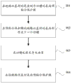
As shown in Figure 1, for the manufacture method of the substrate of a kind of allprint plate of the embodiment of the present invention, comprise the following steps:
Step 101: at the upper surface of insulating properties base material and the lower surface diaphragm of fitting in advance;
Step 102: upper surface and/or lower surface at insulating properties base material are made at least one groove, and make through hole at part or all of groove;
Step 103: at groove and through hole filled conductive ink;
Step 104: remove the insulating properties substrate surface diaphragm of fitting in advance, form the substrate that contains conductor fig.
Wherein, in step 101, the pre-binding temperature of insulating properties base material and diaphragm will be lower than the glass transition temperature of resin in insulating properties base material, and then avoids the resin of insulating properties base material in pre-laminating process to occur to solidify, and loses caking property, the pre-laminating of impact effect.
Diaphragm includes but not limited to polyester film or polyimide film; And because electrically conductive ink has certain mobility, if the thickness of diaphragm is blocked up, removing after diaphragm; the electrically conductive ink that diaphragm place forms groove may flow; cause the coarse problem of conductor fig of formation, therefore, preferably the thickness of diaphragm is less than 25 μ m.
In step 102, as shown in Fig. 2 B 223, can make at least one groove at the upper surface of insulating properties base material or lower surface as required, and make through hole at part or all of groove; As shown in Fig. 3 B 323, also can make at least one groove at the upper surface of insulating properties base material, make groove in the relevant position of the upper surface portion of insulating properties base material or the lower surface that all groove is corresponding.
In step 103, can adopt the mode of printing in the mode of groove and through hole filled conductive ink, wherein, the mode of printing conductive inks as required, can select manual printing, semi-automatic printing, the automatically mode of printing or Vacuum printing, also can as required, several mode of printing collocation be used.
Wherein, the kind of electrically conductive ink includes but not limited to following kind:
Conductive copper ink, conductive silver ink, electric conductive carbon printing ink.
The substrate that contains conductor fig that described in employing Fig. 1, method manufacture forms has two kinds, is introduced respectively below.
The substrate that the first contains conductor fig
The substrate that the first contains conductor fig is to make at least one groove at the upper surface of insulating properties base material or lower surface, and makes through hole at part or all of groove, forms the substrate that one side contains conductor fig.
As shown in Figure 2 A, the manufacture method of the substrate that contains conductor fig for one side, comprising:
Step 201: at the upper surface of insulating properties base material 21 and the lower surface diaphragm 22 of fitting in advance, the procedure chart of step 201 specifically can be referring to 221 of Fig. 2 B;
Step 202: insulating properties base material 21 surfaces at pre-laminating diaphragm 22 process, and make groove 23, and the procedure chart of step 202 specifically can be referring to 222 of Fig. 2 B;
Step 203: in the position of the groove 23 of producing, the processing of holing, produces through hole 24, the procedure chart of step 203 specifically can be referring to 223 of Fig. 2 B;
Step 204: to the groove 23 of producing and through hole 24 filled conductive ink, the procedure chart of step 204 specifically can be referring to 224 of Fig. 2 B;
Step 205: remove the diaphragm of the pre-laminating of insulating properties substrate surface, the procedure chart of step 205 specifically can be referring to 225 of Fig. 2 B.
Wherein, insulating properties base material 21 can be prepreg; Wherein, prepreg includes but not limited to following high molecular polymer:
Epoxy resin glass-fiber-fabric substrate, the weaving cotton cloth of aromatic polyamide resin fiber, epoxy resin nonwoven fabrics substrate, polyimide resin substrate, polyflon substrate, polyphenylene oxide resin substrate, polyphenylene oxide resin substrate, cyanate ester resin substrate, bi-maleimide modified cyanate resin substrate.
Preferably; in step 201, the pre-binding temperature of insulating properties base material 21 and diaphragm 22 will be lower than the glass transition temperature of resin in insulating properties base material, and then avoids the resin of insulating properties base material in pre-laminating process to occur to solidify; lose caking property, the pre-laminating of impact effect.
To fit the in advance processing of diaphragm 22 of insulating properties base material 21, be during for fear of printing conductive inks, ink pollutes insulating properties base material 21 surfaces, causes the conductor fig inaccuracy that forms, or causes the problems such as short circuit.
Wherein, diaphragm includes but not limited to polyester film or polyimide film; And because electrically conductive ink has certain mobility; if the thickness of diaphragm is blocked up, to remove after diaphragm, the electrically conductive ink that diaphragm place forms groove may flow; the coarse problem of conductor fig that causes formation, therefore the thickness of diaphragm is less than 25 μ m.
In step 202, can adopt the method for machining or laser processing, carry out processing and fabricating groove 23 at insulating properties substrate surface, for the problem of the wire dropping on the circuit board of avoiding forming, increase the crystallized ability of conductor fig to wire, the degree of depth of the groove of processing on insulating properties base material should be not less than 5 μ m; Preferably, in order to make the working depth of groove comparatively accurate, can select the method for laser processing groove.
Wherein, the method for laser processing groove includes but not limited to: the method that the method that infrared laser control is profoundly cut and Ultra-Violet Laser control are profoundly cut.
In step 203, make the method that through hole 24 can adopt the method for laser drill or adopt machine drilling, in the time that the diameter in drilled through hole is not less than 0.1mm, adopt the method for machine drilling or laser drill all can, in the time that the diameter in drilled through hole is less than 0.1mm, in order to guarantee the dimensional accuracy in drilled through hole, preferably adopt the method for laser drill to drill through required through hole.
In step 204, can adopt the mode of printing to the mode of the groove 23 of producing and through hole 24 filled conductive ink, wherein mode of printing includes but not limited to following mode of printing: manually printing, semi-automatic printing, the automatically mode of printing or Vacuum printing.According to the needs of printed circuit board (PCB), can select wherein a kind of mode of printing, but also this selects several mode of printings to mix use.
Wherein, the kind of electrically conductive ink includes but not limited to following kind:
Conductive copper ink, conductive silver ink, electric conductive carbon printing ink.
The substrate that the second contains conductor fig
The substrate that the second contains conductor fig is to make at least one groove at the upper surface of insulating properties base material, and make groove in the relevant position of the lower surface that partly or entirely upper surface groove is corresponding, make through hole at part or all of groove, form the two-sided substrate that contains conductor fig.
As shown in 325 of Fig. 3 B, on the two-sided substrate that contains conductor fig, can contain the via of following part or all of kind: the first, upper surface at insulating properties base material is made groove, and makes groove in lower surface same position, between upper surface groove and lower surface groove, makes through hole; The second, at the upper surface groove of insulating properties base material, makes groove in the relevant position of the lower surface of insulating properties base material, between upper surface groove and lower surface groove, make through hole, make the groove of upper surface, the lower surface groove that upper surface groove is corresponding, and corresponding through hole forms path.
On the two-sided substrate that contains conductor fig, also can contain one side via, make a groove at upper surface or the lower surface of insulating properties base material, make through hole at groove, form one side via.
As shown in Figure 3A, be the manufacture method of the two-sided substrate that contains conductor fig, comprising:
Step 301: at the upper surface of insulating properties base material 31 and the lower surface diaphragm 32 of fitting in advance, the procedure chart of step 301 specifically can be referring to 321 of Fig. 3 B;
Step 302: make groove 33 at the pre-laminating insulating properties base material upper surface of diaphragm 32 and the relevant position of lower surface, the procedure chart of step 302 specifically can be referring to 322 of Fig. 3 B;
Step 303: the position of the groove 33 of producing in part, the processing of holing, produces through hole 34, and the procedure chart of step 303 specifically can be referring to 323 of Fig. 3 B;
Step 304: to the groove 33 of producing and through hole 34 filled conductive ink, the procedure chart of step 304 specifically can be referring to 324 of Fig. 3 B;
Step 305: remove the diaphragm of the pre-laminating of insulating properties substrate surface, the procedure chart of step 305 specifically can be referring to 325 of Fig. 3 B.
Wherein, insulating properties base material 31 can make same insulating properties base material with the insulating properties base material 21 in mode one, can be also insulating properties base material not of the same race; Insulating properties base material 31 can be prepreg; Wherein, prepreg includes but not limited to following high molecular polymer:
Epoxy resin glass-fiber-fabric substrate, the weaving cotton cloth of aromatic polyamide resin fiber, epoxy resin nonwoven fabrics substrate, polyimide resin substrate, polyflon substrate, polyphenylene oxide resin substrate, polyphenylene oxide resin substrate, cyanate ester resin substrate, bi-maleimide modified cyanate resin substrate.
Preferably, in step 301, diaphragm 32 can be diaphragm of the same race with the diaphragm 22 in mode one, can be also different diaphragms of planting; And the pre-binding temperature of insulating properties base material 31 and diaphragm 32 will be lower than the glass transition temperature of resin in insulating properties base material, and then avoids the resin of insulating properties base material in pre-laminating process to occur to solidify, and loses caking property, the pre-laminating of impact effect.
To fit the in advance processing of diaphragm 32 of insulating properties base material 31, be during for fear of printing conductive inks, ink pollutes insulating properties base material 31 surfaces, causes the conductor fig inaccuracy that forms, or causes the problems such as short circuit.
Wherein, diaphragm includes but not limited to polyester film or polyimide film; And because electrically conductive ink has certain mobility; if the thickness of diaphragm is blocked up, to remove after diaphragm, the electrically conductive ink that diaphragm place forms groove may flow; the coarse problem of conductor fig that causes formation, therefore the thickness of diaphragm is less than 25 μ m.
In step 302, as shown in Fig. 3 B 323, insulating properties base material upper surface and lower surface at pre-laminating diaphragm 32 are made respectively the groove 33 of requirement, wherein, groove 33 can adopt the method for machining or laser processing, carries out processing and fabricating groove 33 at insulating properties substrate surface, is the problem of the wire dropping on the circuit board of avoiding forming, increase the crystallized ability of conductor fig to wire, the degree of depth of the groove of processing on insulating properties base material should be not less than 5 μ m; Preferably, in order to make the working depth of groove comparatively accurate, can select the method for laser processing groove.
Wherein, the method for laser processing groove includes but not limited to: the method that the method that infrared laser control is profoundly cut and Ultra-Violet Laser control are profoundly cut.
In step 303, make the method that through hole 34 can adopt the method for laser drill or adopt machine drilling, in the time that the diameter in drilled through hole is not less than 0.1mm, adopt the method for machine drilling or laser drill all can, in the time that the diameter in drilled through hole is less than 0.1mm, in order to guarantee the dimensional accuracy in drilled through hole, preferably adopt the method for laser drill to drill through required through hole.
In step 304, can adopt the mode of printing to the mode of the groove 33 of producing and through hole 34 filled conductive ink, wherein mode of printing includes but not limited to following mode of printing: manually printing, semi-automatic printing, the automatically mode of printing or Vacuum printing.According to the needs of printed circuit board (PCB), can select wherein a kind of mode of printing, but also this selects several mode of printings to mix use.
Wherein, the kind of electrically conductive ink includes but not limited to following kind:
Conductive copper ink, conductive silver ink, electric conductive carbon printing ink.
As shown in Figure 4, for the substrate that contains conductive pattern take one side is example, the detailed process of printing conductive inks.
The electrically conductive ink of piling up certain volume at the substrate surface on the groove completing and through hole side, scrapes electrically conductive ink in groove and through hole by scraper, completes the filling of the electrically conductive ink of a groove and through hole, and scraper moves to by next groove.
Wherein, the substrate surface diaphragm of having fitted in advance that electrically conductive ink is piled up, has avoided electrically conductive ink to pollute insulating properties substrate surface, or has caused the coarse problem of conductor fig; And the volume of electrically conductive ink is slightly larger than the volume sum of groove and through hole, to guarantee that electrically conductive ink can be by full to groove and filling through hole.
Wherein, scraper can use rubber scraper or stainless steel scraper.
In the embodiment of the present invention, utilize the substrate manufacture multilayer allprint plate of allprint plate to have two kinds of methods, a kind of is laminating manufacture multilayer allprint plate, another kind of for lamination method manufacture multilayer allprint plate, below two kinds of methods of manufacturing multilayer allprint plates are introduced respectively.
One, laminating is manufactured multilayer allprint plate
As shown in Figure 5, manufacture multilayer allprint plate method for the embodiment of the present invention adopts laminating, comprise the following steps:
Step 501: at least two substrates that contain conductor fig are carried out to lamination processing;
Step 502: the substrate that contains conductor fig after treatment lamination is carried out to pressing processing, form multilayer allprint plate.
Wherein, upper surface and the lower surface of the multilayer allprint plate forming all contain fluted, and the surface of the substrate joint that two of arbitrary neighborhoods contain conductor fig is containing fluted, and each substrate through-hole that contains conductor fig is carried out lamination and the rear superimposed via that forms multilayer allprint plate is processed in pressing, and the superimposed via of the multilayer allprint plate of formation as shown in figure 10.
In step 501, the substrate that contains conductor fig that carries out lamination processing at least contains a two-sided substrate that contains conductive pattern, the manufacture of multilayer allprint plate can have multiple, below take the production method of 4 layers of allprint plate as example, the manufacture of respectively several laminatings being manufactured to multilayer allprint plates is introduced.
Mode one
As shown in Figure 6A, manufacture the manufacture of 4 layers of allprint plate for the first laminating.The substrate that two one sides are contained to conductor fig and a two-sided substrate that contains conductor fig carry out lamination processing, the substrate that substrate, the two-sided substrate that contains conductor fig and the one side that its lamination order contains conductor fig for one side contains conductor fig; The Surface Contact containing reeded surface and the two-sided substrate that contains conductor fig in the substrate that wherein two one sides contain conductor fig; Substrate after treatment lamination is carried out to pressing processing, form 4 layers of allprint plate.
Mode two
As shown in Figure 6B, manufacture the manufacture of 4 layers of allprint plate for the second laminating.The substrate that two one sides are contained to conductor fig and a two-sided substrate that contains conductor fig carry out lamination processing, the substrate that its lamination order contains conductor fig for one side, substrate and the two-sided substrate that contains conductor fig that one side contains conductor fig; Wherein, the substrate that the one side adjacent with the two-sided substrate that contains conductor fig contains conductor fig not containing the surface of groove and the Surface Contact of the two-sided substrate that contains conductor fig, the substrate that the substrate that another one side contains conductor fig does not contain conductor fig containing the surface of groove and adjacent one side contain reeded Surface Contact; Substrate after treatment lamination is carried out to pressing processing, form 4 layers of allprint plate.
Mode three
As shown in Figure 6 C, manufacture the manufacture of 4 layers of allprint plate for the third laminating.Three two-sided substrates that contain conductor fig are carried out to lamination and pressing processing, form 4 layers of allprint plate.
Mode four
As shown in Figure 6 D, it is the manufacture that the 4th kind of laminating manufactured 4 layers of allprint plate, will be only containing reeded substrate, carry out lamination and pressing processing with two two-sided substrates that contain conductor fig, its lamination order, for the two-sided substrate that contains conductor fig, only containing reeded substrate, the two-sided substrate that contains conductor fig, forms 4 layers of allprint plate.
Two, lamination method is manufactured multilayer allprint plate
As shown in Figure 7, manufacture multilayer allprint plate method for the embodiment of the present invention adopts lamination method, comprise the following steps:
Step 701: carry out lamination according to the order of the substrate that contains conductor fig, insulating properties base material and diaphragm;
Step 702: the substrate that contains conductor fig after treatment lamination, insulating properties base material and diaphragm are carried out to pressing processing;
Step 703: make at least one groove on the surface of insulating properties base material;
Step 704: make blind hole at part or all of groove, wherein the position of the groove on insulating properties base material and blind hole forms path with the on-chip groove that contains conductor fig and the through hole that carry out lamination and pressing processing;
Step 705: at groove and described blind hole place filled conductive ink;
Step 706: remove the diaphragm of the pre-laminating of insulating properties substrate surface, form multilayer allprint plate.
Insulating properties base material in step 701 can be prepreg; Wherein, prepreg includes but not limited to following high molecular polymer:
Epoxy resin glass-fiber-fabric substrate, the weaving cotton cloth of aromatic polyamide resin fiber, epoxy resin nonwoven fabrics substrate, polyimide resin substrate, polyflon substrate, polyphenylene oxide resin substrate, polyphenylene oxide resin substrate, cyanate ester resin substrate, bi-maleimide modified cyanate resin substrate.
Preferably; in step 702; right; the two-sided substrate that contains conductor fig; when insulating properties base material and diaphragm carry out pressing, pressing-in temp will be lower than the glass transition temperature of resin in insulating properties base material, and then avoids the resin of insulating properties base material in pre-laminating process to occur to solidify; lose caking property, the pre-laminating of impact effect.
At insulating properties substrate surface pressing diaphragm, be during for fear of printing conductive inks, ink pollutes insulating properties substrate surface, causes the conductor fig inaccuracy that forms, or causes the problems such as short circuit.
Wherein, diaphragm includes but not limited to polyester film or polyimide film; And because electrically conductive ink has certain mobility; if the thickness of diaphragm is blocked up, to remove after diaphragm, the electrically conductive ink that diaphragm place forms groove may flow; the coarse problem of conductor fig that causes formation, therefore the thickness of diaphragm is less than 25 μ m
In step 703, in the time that insulating properties substrate surface is made groove, be the problem of the wire dropping on the circuit board of avoiding forming, increase the crystallized ability of conductor fig to wire, the degree of depth of groove should be not less than 5 μ m; Wherein, the processing method of groove can selector tool the method for processing or laser processing, in order to make the working depth of groove comparatively accurate, preferably select the method for laser processing groove.
Wherein, the method for laser processing groove includes but not limited to: the method that the method that infrared laser control is profoundly cut and Ultra-Violet Laser control are profoundly cut.
In step 704, the making of blind hole can adopt the method for laser drill or adopt the method for machine drilling, in the time that the diameter in drilled through hole is not less than 0.1mm, adopt the method for machine drilling or laser drill all can, in the time that the diameter in drilled through hole is less than 0.1mm, in order to guarantee the dimensional accuracy in drilled through hole, preferably adopt the method for laser drill to drill through required through hole.
Wherein, the thickness after the degree of depth of blind hole is removed groove with insulating properties base material in step 704 is identical; Even if the groove of the groove of making on insulating properties base material and blind hole and the two-sided substrate that contains conductor fig and through hole form path.
In step 705, can adopt the mode of printing to the mode of the groove of producing and blind hole filled conductive ink, wherein mode of printing includes but not limited to following mode of printing: manually printing, semi-automatic printing, the automatically mode of printing or Vacuum printing.According to the needs of printed circuit board (PCB), can select wherein a kind of mode of printing, but also this selects several mode of printings to mix use.
Wherein, the kind of electrically conductive ink includes but not limited to following kind:
Conductive copper ink, conductive silver ink, electric conductive carbon printing ink.
Preferably, in step 701, the substrate that contains conductor fig is the two-sided substrate that contains conductor fig, and the surface contacting with insulating properties base material in the two-sided substrate that contains conductor fig is upper surface and/or lower surface.The upper surface that is the two-sided substrate that contains conductor fig contacts with an insulating properties base material respectively with lower surface, carries out lamination processing; Or the upper surface of the two-sided substrate that contains conductor fig or lower surface contact with an insulating properties base material, carry out lamination processing.
As shown in Figure 8 A, upper surface with the two-sided substrate that contains conductor fig contacts with an insulating properties base material respectively with lower surface, carry out lamination processing, making 4 layers of allprint plate is example, and the method for lamination method being manufactured to multilayer allprint plate is further elaborated.
Step 801: by 82, two diaphragms 83 of 81, two insulating properties base materials of a two-sided substrate that contains conductor fig, carry out lamination processing, the order of lamination is: diaphragm 83, insulating properties base material 82, the two-sided substrate that contains conductor fig 81, insulating properties base material 82 and diaphragm 83; The procedure chart of step 801 specifically can be referring to 821 of Fig. 8 B;
Step 802: by the two-sided substrate that contains conductor fig 81 after treatment lamination, insulating properties base material 82 and diaphragm 83, carry out pressing processing, the procedure chart of step 802 specifically can be referring to 822 of Fig. 8 B;
Step 803: two pressings diaphragm 83 insulating properties base material 82 surface make groove 84, the procedure chart of step 803 specifically can be referring to 823 of Fig. 8 B;
Step 804: the position at the surperficial groove 84 of insulating properties base material 82 makes blind hole 85, wherein, blind hole 85 on insulating properties base material 82 forms path with the through hole of the two-sided substrate that contains conductor fig 81, and the procedure chart of step 804 specifically can be referring to 824 of Fig. 8 B;
Step 805: to the groove groove 84 of producing and blind hole 85 filled conductive ink, the procedure chart of step 805 specifically can be referring to 825 of Fig. 8 B;
Step 806: remove the diaphragm 83 of the insulating properties base material 82 pre-laminatings in surface, the procedure chart of step 806 specifically can be referring to 826 of Fig. 8 B.
As shown in Figure 9 A, the manufacture method of a kind of individual layer allprint plate providing for the embodiment of the present invention, comprises the following steps:
Step 901: the diaphragm 92 of fitting in advance on the surface that need to make groove of insulating properties base material 91, the procedure chart of step 901 specifically can be referring to 921 of Fig. 9 B;
Step 902: the surface at the insulating properties base material 91 of pre-laminating diaphragm 92 makes at least one groove 93, and the procedure chart of step 902 specifically can be referring to 922 of Fig. 9 B;
Step 903: at groove 93 place's filled conductive ink, the procedure chart of step 903 specifically can be referring to 923 of Fig. 9 B;
Step 904: remove the insulating properties base material 91 pre-laminating in surface diaphragms 92, form individual layer allprint plate.
Wherein, insulating properties base material 91 can be prepreg; Wherein, prepreg includes but not limited to following high molecular polymer:
Epoxy resin glass-fiber-fabric substrate, the weaving cotton cloth of aromatic polyamide resin fiber, epoxy resin nonwoven fabrics substrate, polyimide resin substrate, polyflon substrate, polyphenylene oxide resin substrate, polyphenylene oxide resin substrate, cyanate ester resin substrate, bi-maleimide modified cyanate resin substrate.
Preferably; in step 901, the pre-binding temperature of insulating properties base material 91 and diaphragm 92 will be lower than the glass transition temperature of resin in insulating properties base material, and then avoids the resin of insulating properties base material in pre-laminating process to occur to solidify; lose caking property, the pre-laminating of impact effect.
To fit the in advance processing of diaphragm 92 of insulating properties base material 91, be during for fear of printing conductive inks, ink pollutes insulating properties base material 91 surfaces, causes the conductor fig inaccuracy that forms, or causes the problems such as short circuit.
Wherein, diaphragm includes but not limited to polyester film or polyimide film; And because electrically conductive ink has certain mobility; if the thickness of diaphragm is blocked up, to remove after diaphragm, the electrically conductive ink that diaphragm place forms groove may flow; the coarse problem of conductor fig that causes formation, therefore the thickness of diaphragm is less than 25 μ m.
In step 902, can adopt the method for machining or laser processing, carry out processing and fabricating groove 93 at insulating properties substrate surface, for the problem of the wire dropping on the circuit board of avoiding forming, increase the crystallized ability of conductor fig to wire, the degree of depth of the groove of processing on insulating properties base material should be not less than 5 μ m; Preferably, in order to make the working depth of groove comparatively accurate, can select the method for laser processing groove.
Wherein, the method for laser processing groove includes but not limited to: the method that the method that infrared laser control is profoundly cut and Ultra-Violet Laser control are profoundly cut.
In step 903, can adopt the mode of printing to the mode of the groove 93 filled conductive ink of producing, wherein mode of printing includes but not limited to following mode of printing: manually printing, semi-automatic printing, the automatically mode of printing or Vacuum printing.According to the needs of printed circuit board (PCB), can select wherein a kind of mode of printing, but also this selects several mode of printings to mix use.
Wherein, the kind of electrically conductive ink includes but not limited to following kind:
Conductive copper ink, conductive silver ink, electric conductive carbon printing ink.
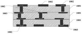
In the embodiment of the present invention, multilayer allprint plate is to be obtained by laminating by some substrates that contain conductor fig, or obtained by lamination method by the substrate that contains conductor fig and insulating properties base material, take 4 layers of allprint plate as example, shown in Figure 10, the structure of 4 layers of allprint plate is described below.
These 4 layers of allprint plates are made up of three insulating properties base materials, and the upper surface of each insulating properties base material 1001 and/or lower surface contain several grooves 1002, contain through hole 1003 on part groove, in groove 1002 and through hole 1003, are filled with electrically conductive ink.
As shown in figure 11, be the structure of a kind of substrate of allprint plate in the embodiment of the present invention.
The substrate of this allprint plate comprises an insulating properties base material 1101, upper surface on this insulating properties base material 1101 and/or lower surface contain at least one groove 1102, at part or all of groove, through hole 1103 is contained at 1102 places, in groove 1102 and through hole 1103, is filled with electrically conductive ink.
As shown in figure 12, be the structure of a kind of multilayer allprint plate in the embodiment of the present invention.
This multilayer allprint plate comprises the substrate 1201 of several allprint plates, upper surface and/or lower surface at insulating properties base material 1201 contain at least one groove 1102, at part or all of groove, through hole 1103 is contained at 1102 places, in groove 1102 and through hole 1103, is filled with electrically conductive ink.
As shown in figure 13, be the structure of a kind of individual layer allprint plate in the embodiment of the present invention.
This individual layer allprint plate comprises an insulating properties base material 1301, contains at least one groove 1302 on this insulating properties base material 1301, in groove 1302, is filled with electrically conductive ink.
Obviously, those skilled in the art can carry out various changes and modification and not depart from the spirit and scope of the present invention the present invention.Like this, if within of the present invention these are revised and modification belongs to the scope of the claims in the present invention and equivalent technologies thereof, the present invention is also intended to comprise these changes and modification interior.
Claims (12)
1. a manufacture method for the substrate of allprint plate, is characterized in that, the method comprises:
At the upper surface of insulating properties base material and the lower surface diaphragm of fitting in advance;
Upper surface and/or lower surface at insulating properties base material are made at least one groove, and make through hole at part or all of groove;
At described groove and described through hole filled conductive ink;
Remove the insulating properties substrate surface diaphragm of fitting in advance, form the substrate that contains conductor fig.
2. the method for claim 1, is characterized in that, makes at least one groove at upper surface and the lower surface of insulating properties base material, and makes through hole at part or all of groove, comprising:
A groove of making at the upper surface of insulating properties base material, and a groove of making at lower surface corresponding to this groove, and the through hole of making on this upper surface groove forms an electrical connection path of this insulating properties base material jointly.
3. utilize substrate that claim 2 makes to manufacture a method for allprint plate, it is characterized in that, the method also comprises:
The substrate that contains conductor fig described at least two of formation is carried out to lamination and pressing processing, form multilayer allprint plate;
Wherein, upper surface and the lower surface of described multilayer allprint plate all contain fluted, and the surface of the substrate joint of containing conductor fig described in two of arbitrary neighborhoods is containing fluted, and the substrate through-hole that contains conductor fig described in each carries out forming after lamination and pressing are processed the superimposed via of multilayer allprint plate.
4. the substrate that utilizes claim 1 or 2 to make is manufactured a method for allprint plate, it is characterized in that, the method comprises:
Carry out lamination and pressing processing according to the order of the substrate that contains conductor fig, insulating properties base material and diaphragm, the wherein said substrate that contains conductor fig is the substrate that upper and lower surface all contains reeded conductor fig, and the surface contacting with insulating properties base material in the substrate that contains conductor fig is upper surface and/or lower surface;
Make at least one groove on the surface of insulating properties base material, and make blind hole at part or all of groove;
At described groove and described blind hole place filled conductive ink, remove the diaphragm of the pre-laminating of insulating properties substrate surface, form multilayer allprint plate.
5. method as claimed in claim 4, is characterized in that, after forming multilayer allprint plate, also comprises:
Whether the number of plies that judges multilayer allprint plate meets the setting number of plies; if; shut-down operation; otherwise; carry out lamination and pressing processing according to the order of multilayer allprint plate, insulating properties base material and diaphragm, and return to the whether satisfied step of setting the number of plies of the number of plies that judges multilayer allprint plate.
6. a manufacture method for allprint plate, is characterized in that, the method comprises:
The surface that needs to make groove on the insulating properties base material diaphragm of fitting in advance, and make at least one groove on the surface of pre-laminating diaphragm;
At described groove filled conductive ink;
Remove the insulating properties substrate surface diaphragm of fitting in advance, form individual layer allprint plate.
7. a multilayer allprint plate, is characterized in that, this circuit board comprises:
At least two substrates that contain conductor fig;
Wherein, the upper surface of this multilayer allprint plate and lower surface all contain fluted, contain through hole at part or all of groove, and the surface of any two adjacent substrate joints of containing conductor fig is containing fluted; In described groove and described through hole, be filled with electrically conductive ink.
8. circuit board as claimed in claim 7, is characterized in that, described in contain conductor fig substrate also comprise:
On the upper surface of the described substrate that contains conductor fig and/or lower surface, contain at least one groove, and partly or entirely on the position of groove, contain through hole, in groove and through hole, be filled with electrically conductive ink.
9. circuit board as claimed in claim 8, is characterized in that, on the upper surface of the described substrate that contains conductor fig and/or lower surface, contains at least one groove, comprising:
The groove that the upper surface of insulating properties base material contains, and a groove of lower surface corresponding to this groove, and the through hole containing on this upper surface groove forms an electrical connection path of this insulating properties base material jointly.
10. a substrate for allprint plate, is characterized in that, this substrate comprises:
Upper surface and/or lower surface at insulating properties base material at least contain a groove, and contain through hole at part or all of groove;
Be filled with electrically conductive ink at described groove and described through hole.
11. 1 kinds of allprint plates, is characterized in that, comprise substrate as claimed in claim 10.
12. 1 kinds of individual layer allprint plates, is characterized in that, this circuit board comprises:
An insulating properties base material contains at least one groove on this insulating properties base material, is filled with electrically conductive ink in groove.
Priority Applications (1)
| Application Number | Priority Date | Filing Date | Title |
|---|---|---|---|
| CN201210450725.1A CN103813640A (en) | 2012-11-12 | 2012-11-12 | All printed circuit board and manufacturing method thereof |
Applications Claiming Priority (1)
| Application Number | Priority Date | Filing Date | Title |
|---|---|---|---|
| CN201210450725.1A CN103813640A (en) | 2012-11-12 | 2012-11-12 | All printed circuit board and manufacturing method thereof |
Publications (1)
| Publication Number | Publication Date |
|---|---|
| CN103813640A true CN103813640A (en) | 2014-05-21 |
Family
ID=50709668
Family Applications (1)
| Application Number | Title | Priority Date | Filing Date |
|---|---|---|---|
| CN201210450725.1A Pending CN103813640A (en) | 2012-11-12 | 2012-11-12 | All printed circuit board and manufacturing method thereof |
Country Status (1)
| Country | Link |
|---|---|
| CN (1) | CN103813640A (en) |
Cited By (10)
| Publication number | Priority date | Publication date | Assignee | Title |
|---|---|---|---|---|
| CN104093279A (en) * | 2014-07-16 | 2014-10-08 | 电子科技大学 | Printed-circuit board manufacturing method based on laser groove machining technology |
| CN107087355A (en) * | 2017-06-16 | 2017-08-22 | 东莞职业技术学院 | A kind of method that use screen printing technique realizes the interconnection of PCB internal layers |
| CN110324991A (en) * | 2019-07-10 | 2019-10-11 | 广东工业大学 | A kind of preparation method of composite circuit board |
| CN110536551A (en) * | 2019-07-10 | 2019-12-03 | 广东工业大学 | A kind of preparation method of circuit board |
| CN112533386A (en) * | 2020-12-24 | 2021-03-19 | 深圳市百柔新材料技术有限公司 | Manufacturing method of conductive circuit board |
| WO2022006789A1 (en) * | 2020-07-08 | 2022-01-13 | 广东工业大学 | Method for preparing composite circuit board |
| CN114007346A (en) * | 2021-10-26 | 2022-02-01 | 武汉天喻信息产业股份有限公司 | Multilayer circuit board manufacturing method and multilayer circuit board |
| CN114126224A (en) * | 2020-08-28 | 2022-03-01 | 深南电路股份有限公司 | Circuit board and manufacturing method thereof |
| US11348831B2 (en) | 2019-07-04 | 2022-05-31 | Universal Global Technology (Shanghai) Co., Ltd | Method of manufacturing a semiconductor unit |
| TWI803185B (en) * | 2022-02-10 | 2023-05-21 | 福懋科技股份有限公司 | Printing device |
Citations (4)
| Publication number | Priority date | Publication date | Assignee | Title |
|---|---|---|---|---|
| JP2000232267A (en) * | 1999-02-12 | 2000-08-22 | Matsushita Electric Ind Co Ltd | Manufacture of multilayer printed wiring board |
| CN101466205A (en) * | 2007-12-19 | 2009-06-24 | 富葵精密组件(深圳)有限公司 | Circuit board and preparation method thereof |
| CN101610635A (en) * | 2008-06-20 | 2009-12-23 | 欣兴电子股份有限公司 | Circuit board structure and technology thereof |
| CN102595809A (en) * | 2012-03-14 | 2012-07-18 | 柏承科技(昆山)股份有限公司 | Method for manufacturing high-density interconnection printed circuit board |
-
2012
- 2012-11-12 CN CN201210450725.1A patent/CN103813640A/en active Pending
Patent Citations (4)
| Publication number | Priority date | Publication date | Assignee | Title |
|---|---|---|---|---|
| JP2000232267A (en) * | 1999-02-12 | 2000-08-22 | Matsushita Electric Ind Co Ltd | Manufacture of multilayer printed wiring board |
| CN101466205A (en) * | 2007-12-19 | 2009-06-24 | 富葵精密组件(深圳)有限公司 | Circuit board and preparation method thereof |
| CN101610635A (en) * | 2008-06-20 | 2009-12-23 | 欣兴电子股份有限公司 | Circuit board structure and technology thereof |
| CN102595809A (en) * | 2012-03-14 | 2012-07-18 | 柏承科技(昆山)股份有限公司 | Method for manufacturing high-density interconnection printed circuit board |
Cited By (10)
| Publication number | Priority date | Publication date | Assignee | Title |
|---|---|---|---|---|
| CN104093279A (en) * | 2014-07-16 | 2014-10-08 | 电子科技大学 | Printed-circuit board manufacturing method based on laser groove machining technology |
| CN107087355A (en) * | 2017-06-16 | 2017-08-22 | 东莞职业技术学院 | A kind of method that use screen printing technique realizes the interconnection of PCB internal layers |
| US11348831B2 (en) | 2019-07-04 | 2022-05-31 | Universal Global Technology (Shanghai) Co., Ltd | Method of manufacturing a semiconductor unit |
| CN110324991A (en) * | 2019-07-10 | 2019-10-11 | 广东工业大学 | A kind of preparation method of composite circuit board |
| CN110536551A (en) * | 2019-07-10 | 2019-12-03 | 广东工业大学 | A kind of preparation method of circuit board |
| WO2022006789A1 (en) * | 2020-07-08 | 2022-01-13 | 广东工业大学 | Method for preparing composite circuit board |
| CN114126224A (en) * | 2020-08-28 | 2022-03-01 | 深南电路股份有限公司 | Circuit board and manufacturing method thereof |
| CN112533386A (en) * | 2020-12-24 | 2021-03-19 | 深圳市百柔新材料技术有限公司 | Manufacturing method of conductive circuit board |
| CN114007346A (en) * | 2021-10-26 | 2022-02-01 | 武汉天喻信息产业股份有限公司 | Multilayer circuit board manufacturing method and multilayer circuit board |
| TWI803185B (en) * | 2022-02-10 | 2023-05-21 | 福懋科技股份有限公司 | Printing device |
Similar Documents
| Publication | Publication Date | Title |
|---|---|---|
| CN103813640A (en) | All printed circuit board and manufacturing method thereof | |
| CN108684155B (en) | Method for embedding resistor in printed circuit board | |
| CN104125724B (en) | Production process for PCB (Printed Circuit Board) metal half-hole products | |
| CN103456643A (en) | Ic carrier plate and manufacturing method thereof | |
| CN102480852B (en) | Method for manufacturing circuit boards | |
| CN103906364B (en) | A kind of processing method of buried resistor in printed circuit board | |
| CN104125727A (en) | Method for manufacturing rigid-flexible printed circuit board with multiple layers of soft boards | |
| CN101120623A (en) | Manufacturing method of multi-layer circuit board and multi-layer circuit board | |
| CN103108491A (en) | Circuit board and manufacture method thereof | |
| CN104349574A (en) | Circuit board and manufacturing method thereof | |
| CN105188278A (en) | Resin plug hole stitching structure and resin plug hole technology | |
| CN104519680A (en) | Ecological method for constructing circuit boards | |
| CN103108485A (en) | Multi-layer printed circuit board and manufacturing method thereof | |
| CN104717840A (en) | Circuit board manufacturing method and circuit board | |
| TWI501715B (en) | Multilayer printed circuit board and manufacturing method thereof | |
| CN102227959B (en) | Wiring board and method for manufacturing same | |
| CN104254213A (en) | Multi-layer circuit board and manufacturing method thereof | |
| CN103841771A (en) | Combined printed circuit board manufacturing method and printed circuit board | |
| CN104735899B (en) | Flexible circuit board and preparation method thereof | |
| CN106061140A (en) | High-order random-layer HDI board manufacture process | |
| CN103857176A (en) | Circuit board and manufacture method for the same | |
| CN103906376A (en) | Flexible circuit board and manufacturing method thereof | |
| CN104159392A (en) | Printed circuit board and preparation method thereof | |
| CN103144378B (en) | Copper-clad plate (CCL) and printed circuit board (PCB) of phenol novolac (PN) curing system and manufacturing method thereof | |
| CN101951737A (en) | Manufacture method of multilayered circuit board |
Legal Events
| Date | Code | Title | Description |
|---|---|---|---|
| C06 | Publication | ||
| PB01 | Publication | ||
| C10 | Entry into substantive examination | ||
| SE01 | Entry into force of request for substantive examination | ||
| RJ01 | Rejection of invention patent application after publication | ||
| RJ01 | Rejection of invention patent application after publication |
Application publication date: 20140521 |