CN102687262A - Semiconductor wafer transport system - Google Patents
Semiconductor wafer transport system Download PDFInfo
- Publication number
- CN102687262A CN102687262A CN2010800586516A CN201080058651A CN102687262A CN 102687262 A CN102687262 A CN 102687262A CN 2010800586516 A CN2010800586516 A CN 2010800586516A CN 201080058651 A CN201080058651 A CN 201080058651A CN 102687262 A CN102687262 A CN 102687262A
- Authority
- CN
- China
- Prior art keywords
- plate
- wafer
- locator
- outlet
- location
- Prior art date
- Legal status (The legal status is an assumption and is not a legal conclusion. Google has not performed a legal analysis and makes no representation as to the accuracy of the status listed.)
- Pending
Links
Images


Classifications
-
- H—ELECTRICITY
- H01—ELECTRIC ELEMENTS
- H01L—SEMICONDUCTOR DEVICES NOT COVERED BY CLASS H10
- H01L21/00—Processes or apparatus adapted for the manufacture or treatment of semiconductor or solid state devices or of parts thereof
- H01L21/67—Apparatus specially adapted for handling semiconductor or electric solid state devices during manufacture or treatment thereof; Apparatus specially adapted for handling wafers during manufacture or treatment of semiconductor or electric solid state devices or components ; Apparatus not specifically provided for elsewhere
- H01L21/683—Apparatus specially adapted for handling semiconductor or electric solid state devices during manufacture or treatment thereof; Apparatus specially adapted for handling wafers during manufacture or treatment of semiconductor or electric solid state devices or components ; Apparatus not specifically provided for elsewhere for supporting or gripping
- H01L21/6838—Apparatus specially adapted for handling semiconductor or electric solid state devices during manufacture or treatment thereof; Apparatus specially adapted for handling wafers during manufacture or treatment of semiconductor or electric solid state devices or components ; Apparatus not specifically provided for elsewhere for supporting or gripping with gripping and holding devices using a vacuum; Bernoulli devices
-
- B—PERFORMING OPERATIONS; TRANSPORTING
- B25—HAND TOOLS; PORTABLE POWER-DRIVEN TOOLS; MANIPULATORS
- B25J—MANIPULATORS; CHAMBERS PROVIDED WITH MANIPULATION DEVICES
- B25J11/00—Manipulators not otherwise provided for
- B25J11/0095—Manipulators transporting wafers
-
- B—PERFORMING OPERATIONS; TRANSPORTING
- B25—HAND TOOLS; PORTABLE POWER-DRIVEN TOOLS; MANIPULATORS
- B25J—MANIPULATORS; CHAMBERS PROVIDED WITH MANIPULATION DEVICES
- B25J15/00—Gripping heads and other end effectors
- B25J15/06—Gripping heads and other end effectors with vacuum or magnetic holding means
- B25J15/0616—Gripping heads and other end effectors with vacuum or magnetic holding means with vacuum
-
- B—PERFORMING OPERATIONS; TRANSPORTING
- B65—CONVEYING; PACKING; STORING; HANDLING THIN OR FILAMENTARY MATERIAL
- B65G—TRANSPORT OR STORAGE DEVICES, e.g. CONVEYORS FOR LOADING OR TIPPING, SHOP CONVEYOR SYSTEMS OR PNEUMATIC TUBE CONVEYORS
- B65G49/00—Conveying systems characterised by their application for specified purposes not otherwise provided for
- B65G49/05—Conveying systems characterised by their application for specified purposes not otherwise provided for for fragile or damageable materials or articles
- B65G49/06—Conveying systems characterised by their application for specified purposes not otherwise provided for for fragile or damageable materials or articles for fragile sheets, e.g. glass
- B65G49/063—Transporting devices for sheet glass
- B65G49/064—Transporting devices for sheet glass in a horizontal position
- B65G49/065—Transporting devices for sheet glass in a horizontal position supported partially or completely on fluid cushions, e.g. a gas cushion
-
- H—ELECTRICITY
- H01—ELECTRIC ELEMENTS
- H01L—SEMICONDUCTOR DEVICES NOT COVERED BY CLASS H10
- H01L21/00—Processes or apparatus adapted for the manufacture or treatment of semiconductor or solid state devices or of parts thereof
- H01L21/67—Apparatus specially adapted for handling semiconductor or electric solid state devices during manufacture or treatment thereof; Apparatus specially adapted for handling wafers during manufacture or treatment of semiconductor or electric solid state devices or components ; Apparatus not specifically provided for elsewhere
- H01L21/677—Apparatus specially adapted for handling semiconductor or electric solid state devices during manufacture or treatment thereof; Apparatus specially adapted for handling wafers during manufacture or treatment of semiconductor or electric solid state devices or components ; Apparatus not specifically provided for elsewhere for conveying, e.g. between different workstations
- H01L21/67739—Apparatus specially adapted for handling semiconductor or electric solid state devices during manufacture or treatment thereof; Apparatus specially adapted for handling wafers during manufacture or treatment of semiconductor or electric solid state devices or components ; Apparatus not specifically provided for elsewhere for conveying, e.g. between different workstations into and out of processing chamber
- H01L21/67742—Mechanical parts of transfer devices
-
- H—ELECTRICITY
- H01—ELECTRIC ELEMENTS
- H01L—SEMICONDUCTOR DEVICES NOT COVERED BY CLASS H10
- H01L21/00—Processes or apparatus adapted for the manufacture or treatment of semiconductor or solid state devices or of parts thereof
- H01L21/67—Apparatus specially adapted for handling semiconductor or electric solid state devices during manufacture or treatment thereof; Apparatus specially adapted for handling wafers during manufacture or treatment of semiconductor or electric solid state devices or components ; Apparatus not specifically provided for elsewhere
- H01L21/683—Apparatus specially adapted for handling semiconductor or electric solid state devices during manufacture or treatment thereof; Apparatus specially adapted for handling wafers during manufacture or treatment of semiconductor or electric solid state devices or components ; Apparatus not specifically provided for elsewhere for supporting or gripping
- H01L21/687—Apparatus specially adapted for handling semiconductor or electric solid state devices during manufacture or treatment thereof; Apparatus specially adapted for handling wafers during manufacture or treatment of semiconductor or electric solid state devices or components ; Apparatus not specifically provided for elsewhere for supporting or gripping using mechanical means, e.g. chucks, clamps or pinches
- H01L21/68707—Apparatus specially adapted for handling semiconductor or electric solid state devices during manufacture or treatment thereof; Apparatus specially adapted for handling wafers during manufacture or treatment of semiconductor or electric solid state devices or components ; Apparatus not specifically provided for elsewhere for supporting or gripping using mechanical means, e.g. chucks, clamps or pinches the wafers being placed on a robot blade, or gripped by a gripper for conveyance
-
- B—PERFORMING OPERATIONS; TRANSPORTING
- B65—CONVEYING; PACKING; STORING; HANDLING THIN OR FILAMENTARY MATERIAL
- B65G—TRANSPORT OR STORAGE DEVICES, e.g. CONVEYORS FOR LOADING OR TIPPING, SHOP CONVEYOR SYSTEMS OR PNEUMATIC TUBE CONVEYORS
- B65G2249/00—Aspects relating to conveying systems for the manufacture of fragile sheets
- B65G2249/04—Arrangements of vacuum systems or suction cups
- B65G2249/045—Details of suction cups suction cups
Landscapes
- Engineering & Computer Science (AREA)
- Physics & Mathematics (AREA)
- Condensed Matter Physics & Semiconductors (AREA)
- General Physics & Mathematics (AREA)
- Manufacturing & Machinery (AREA)
- Computer Hardware Design (AREA)
- Microelectronics & Electronic Packaging (AREA)
- Power Engineering (AREA)
- Robotics (AREA)
- Mechanical Engineering (AREA)
- Container, Conveyance, Adherence, Positioning, Of Wafer (AREA)
Abstract
A system and a wand are disclosed for the transport of a semiconductor wafer. The system and wand include a plate and a locator. The plate includes a plurality of plate outlets for directing a gas flow against the wafer to hold the wafer using the Bernoulli principle. The locator extends from the plate and includes a locating outlet for directing a gas flow to locate the wafer laterally relative to the plate. The plate outlets and the locating outlet operate to prevent the wafer from contacting the plate or the locator. In some embodiments, a plurality of locators are used to locate the wafer laterally relative to the plate.
Description
Background technology
Semiconductor wafer is moved by " Bernoulli wand (Bernoulli wand) " during process operation usually.Said Bernoulli wand utilizes bernoulli principle directly below said rod, to form slipstream (pocket).Said slipstream is through being formed by the increase of gas flow speed when the downside of said rod is drawn at gas.Said slipstream attracts wafer towards the lower surface of said rod, and gas flow has stoped the following side contacts of the top surface and the said rod of wafer simultaneously.Be provided with outstanding leg downwards in the edge of said rod, so that along the lateral register wafer and prevent below said rod, to skid off at wafer during the said rod motion.The leg of said rod comes positions wafer through the edge of contact wafer.Because Bernoulli wand is used in the hot environment usually, therefore said rod and leg are processed by resistant to elevated temperatures quartz or other material.Thereby submissive materials such as plastics is not suitable for being used on the leg of said rod to alleviate or to relax the contact between the leg of Waffer edge and said rod.
Summary of the invention
One aspect of the present invention is a kind of semiconductor wafer conveying system that comprises plate and locator.Said plate comprises a plurality of plate exits, is used for facing to wafer guiding gas stream so that utilize bernoulli principle to keep wafer.Said locator extends from said plate, and comprises the location outlet that is used for guiding gas stream, so as with respect to said plate along the lateral register wafer.Said plate exit is operated to prevent that wafer from contacting with said plate or locator with the location outlet.
Another aspect is a kind of rod that comprises plate and a plurality of locators (wand) that is used for transfer wafers.Said plate comprises a plurality of plate exits, is used for facing to wafer guiding gas stream so that utilize bernoulli principle to keep wafer.Said plate has neck to help to locate said plate.Said a plurality of locator extends from said plate, and includes the location outlet that is used for guiding gas stream, so as with respect to said plate along the lateral register wafer.Said plate exit is operated to prevent that wafer from contacting with said plate or locator with the location outlet.
There are various improvement for the characteristic of mentioning in the above-mentioned each side.Further feature also can be combined in the above-mentioned each side.These improve and supplementary features can individually or exist with any combination.For example, the various characteristics of discussing among the embodiment of hereinafter shown in any can be individually or be combined in any compound mode any above-mentioned aspect in.
Description of drawings
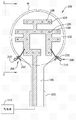
Fig. 1 is a kind of plan view from above of exemplary rod;
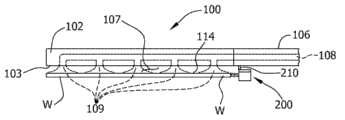
Fig. 2 is the partial side view of the exemplary rod of Fig. 1;
Fig. 3 is a kind of plan view from above of exemplary excellent leg;
Fig. 4 is the end view of the exemplary excellent leg of Fig. 3; And
Fig. 5 is the plan view from above of the excellent leg of another embodiment.
Embodiment
The wafer W that Fig. 1 and 2 illustrates a kind of exemplary Bernoulli wand 100 (being called " rod " hereinafter) and is positioned at the rod below.In this exemplary embodiment, wafer W is a semiconductor wafer, and can carry any substrate through rod 100 in other embodiments.Fig. 1 is the plan view from above of rod 100, and Fig. 2 is the end view of the part of rod.The rod of this embodiment is suitable for delivery diameter and is 200mm or 300mm or the wafer of 400mm at least at least at least, perhaps is suitable for delivery diameter in certain embodiments and is the wafer of 450mm at least.
The plate 102 of rod 100 has a plurality of inner passages 108 or groove, so that guiding gas stream therefrom passes through.Inner passage 108 guiding are passed through excellent 100 neck 106, the inside of the entering plate 102 of going forward side by side from the gas stream of gas source 112.Gas stream leaves rod 100 through a plurality of plate exits 109 in the lower surface 103 of plate 102.The gas stream that leaves plate 102 is shown in broken lines in Fig. 2.In said a plurality of plate exit 109 each is communicated with at least a portion fluid of inner passage 108.In this exemplary embodiment, the shape of said a plurality of plate exits 109 is circular, but plate exit can have difformity (for example, shape of slit) in different embodiment.
In this exemplary embodiment, plate exit 109 is configured to: their guiding gas stream at a certain angle when gas leaves plate 102.In certain embodiments, according to the position of different plate exit 109 on plate 102, said angle is different for these different plate exits 109.The angular deflection (angling) of the gas stream through plate exit 109 is with a part of bias voltage of wafer W towards rod 100.For example, wafer W can be biased on the direction of one or more locators (that is a pair of excellent leg of, discussing like hereinafter).In this exemplary embodiment, plate exit 109 is the openings that in the lower surface 103 of plate 102, form.Be conducted through inner passage 108 and be can be sharply and any suitable inert gas (for example, argon or nitrogen) of wafer W reaction via the specific gas that plate exit 109 flows out.
When gas leaves plate exit 109, according to forming low-pressure area in the zone 107 of bernoulli principle between the lower surface 103 of wafer W and plate 102.This low-pressure area is produced by said gas when gas leaves plate 102 through plate exit 109.This low-pressure area causes producing the lifting force that attracts wafer W towards the lower surface 103 of plate 102.When the top surface 114 of wafer W was attracted the lower surface 103 near plate 102, the gas stream through the plate exit 109 of flowing through had stoped said top surface to contact said lower surface.Although the gas stream through plate exit 109 is enough to respect to excellent 100 wafer W vertically is held in place, the lifting force that is produced through flowing can not be settled or positions wafer along side direction.
Shown in Fig. 3 and 4, a pair of leg 200 (broadly for " locator ") stretch out from the edge 101 of rod 100 and from the lower surface 103 of rod 100 to extending below.Usually, leg 200 with respect to rod 100 along the lateral register wafer W.Although show a pair of leg 200 in this exemplary embodiment, can use any amount of leg and can not depart from the scope of embodiment.For example, except said a pair of leg 200, can use the 3rd leg.Said the 3rd leg can said neck 106 places or near be positioned between the said a pair of leg 200, and be configured to prevent wafer W rotation.The same as rod 100, leg 200 constitutes (for example quartzy) by resistant to elevated temperatures material.
Each leg 200 has the supporting structure 210 that liner 220 is attached to rod 100.Be formed with inner passage 230 or groove in the supporting structure 210, be used for supplied gas and flow through this supporting structure and export 240 outflows via the location.The same as plate exit 109, said location outlet 240 can be parallel to the plane that is limited plate 102 and guide the gas stream that leaves through said location outlet 240.In one embodiment, gas stream can change between+/-10 degree with respect to said plane through orienting mouthfuls 240 angles left, perhaps in another embodiment, between+/-30 degree, changes.In this exemplary embodiment, on the liner 220 of leg 200, have five location outlets 240, other embodiment can use more or less outlet and can not depart from the scope of embodiment.In addition, although the location shown in accompanying drawing outlet 240 be shaped as circle, can use difform outlet and can not depart from the scope of embodiment.For example, in one embodiment, location outlet 240 is the slit on the plane that totally is parallel to plate 102 of formation in liner 220.
The inner passage 230 of supporting structure 210 is communicated with inner passage 108 fluids of plate 102, and by identical gas source 112 supply gas.Can use any suitable connector the inner passage 230 of supporting structure 210 to be connected to the inner passage 108 of plate 102.In other embodiments, the inner passage 230 of supporting structure 210 can not be connected to the inner passage 108 of plate.On the contrary, inner passage 230 can directly be connected to gas source 112.Although a pair of leg 200 has been shown among Fig. 1 and 2, can uses any amount of leg and can not depart from the scope of embodiment.In one embodiment, an additional leg is positioned on the plate 102 so that be bonded on the recess that forms in the edge of wafer W.Joint between said additional leg and the said recess has prevented that wafer W is with respect to plate 102 rotations.
In another embodiment shown in Fig. 5, gas stream is not introduced to supporting structure 210 inside.On the contrary, gas stream is crossed the external pipe 250 that adjacent support structure 210 is provided with.Pipeline 250 is made up of resistant to elevated temperatures material (for example quartzy).Pipeline 250 liner 220 places or near end at pipe outlet 260, and on the direction identical with the embodiment that uses location outlet 240 guiding gas stream.In the embodiment of Fig. 5, used three pipe outlets 260, but can use more or less pipe outlet and can not depart from the scope of embodiment.
In operation, rod 100 is used for not comprising transfer wafers W under the situation that edge physics contacts with any part of wafer in wafer process operating period.In conventional Bernoulli wand, the edge of wafer contacts with excellent leg.Contacting between Waffer edge and the excellent leg can damage the edge.The damage that Waffer edge is caused possibly cause wafer can not satisfy quality standard or make that wafer is not suitable for being used in the device.
In one embodiment; Rod 100 is transported to wafer W in the epitaxial reactor (epitaxial reactor); Wafer W experiences epitaxial process in 1050 ℃ to 1200 ℃ hot environment in this reactor, and said rod can stand 600 ℃ to 950 ℃ temperature.After growth course is accomplished, wafer W is removed from reactor through excellent 100.During mentioning wafer W, gas is conducted through rod 100 inner passage 108 and flows out via plate opening 109 from gas source 112.One of them a little plate opening 109 is angled with respect to the plane that is limited plate 102, makes gas stream biasing wafer W on the direction of leg 200.Gas also is conducted through the inner passage 108 of rod 100 and gets into the inner passage 230 of the supporting structure of leg 200.Gas flows out from leg through locator outlet 240 then.Therefore gas is flowing in biasing wafer W on the direction of leg 200 through some of them plate opening 109 at least angled.Gas contacts with liner 220 entering of leg through the mobile edge of wafer W that prevented of locator outlet 240.
In certain embodiments, on many edges that leg 200 are positioned at plate 102.In these embodiment, plate exit 109 can be not angled because wafer W need be not biased on the direction of any leg 200, this be because through said many to leg prevented wafer with respect to rod 100 along being displaced sideways.In these embodiment, leg 200 can be positioned at the equidistant position on the edge of plate 102, to prevent being displaced sideways of wafer W.
When introducing the element of the present invention or embodiment, article " ", " being somebody's turn to do " and " said " are intended to mean to have one or more elements.Term " comprises ", " comprising " and " having " comprising property, and meaning except the element of listing to have additional element.
Owing to can carry out various changes and can not depart from scope of the present invention to above structure, therefore comprise in the above specification and accompanying drawing shown in all the elements should be interpreted as exemplary, rather than restrictive.
Claims (20)
1. semiconductor wafer conveying system that is used for transport semiconductor wafers comprises:
The plate that comprises a plurality of plate exits, said plate exit are used for facing to wafer guiding gas stream so that utilize bernoulli principle to keep wafer;
Extend and comprise the locator of location outlet from said plate, the outlet of said location be used for guiding gas stream in case with respect to said plate along the lateral register wafer;
Wherein, said plate exit is operated to prevent that wafer from contacting with said plate or locator with the location outlet.
2. system according to claim 1 is characterized in that said plate limits a plane, and the outlet of said location is to become the angle guiding gas of 0 degree to 30 degree with respect to said plane.
3. system according to claim 1 is characterized in that, the outlet of said location is totally to be parallel to the slit that extend on the plane of said plate.
4. system according to claim 1; It is characterized in that; Said locator is first locator, and said system comprises also and isolated second locator of said first locator that said second locator is from said plate extension and comprise the location outlet that is used for respect to said plate positions wafer.
5. system according to claim 1 is characterized in that, is provided with groove in the said plate, and said groove is connected to gas vent with gas source.
6. system according to claim 5; It is characterized in that; Said system also comprises the neck that extends from said plate, and from the arm that the said neck that is used to locate said plate extends, comprises groove in the said neck to be used for gas source is connected to the groove of said plate.
7. system according to claim 1 is characterized in that said system combines with semiconductor wafer, and the diameter of said wafer is 300mm at least.
8. rod that is used for transfer wafers, said rod comprises:
The plate that comprises a plurality of plate exits, said plate exit are used for flowing so that utilize bernoulli principle to keep wafer facing to the wafer guiding gas, and said plate has neck to help to locate said plate;
Extend and comprise respectively a plurality of locators of location outlet from said plate, the outlet of said location be used for guiding gas stream in case with respect to said plate along the lateral register wafer;
Wherein, said plate exit is operated to prevent that wafer from contacting with said plate or locator with the location outlet.
9. rod according to claim 8 is characterized in that said plate limits a plane, and one of them location outlet is to become the angle guiding gas of 0 degree to 10 degree with respect to said plane.
10. rod according to claim 9 is characterized in that, at least one plate exit is different with respect to the angle of said plane guiding gas and another plate exit at least with respect to the angle of said plane guiding gas.
11. rod according to claim 9 is characterized in that, at least one plate exit is at least one the locator biasing wafer in said a plurality of locators with respect to the angle Selection of said plane guiding gas.
12. rod according to claim 8 is characterized in that, said plate exit be shaped as circle.
13. rod according to claim 8 is characterized in that, a locator in said a plurality of locators is configured to and is located at the engage on the edge of wafer.
14. rod according to claim 8 is characterized in that, each locator in said a plurality of locators is spaced apart from each other.
15. rod according to claim 14 is characterized in that, said plate is circular, and said locator is evenly spaced apart each other along the circumference of said plate.
16. rod according to claim 8 is characterized in that, said plate and said a plurality of locator are processed by quartz.
17. rod according to claim 8 is characterized in that, is provided with groove in the said plate, said groove is connected to plate exit with gas source.
18. rod according to claim 17 is characterized in that, is equipped with groove in said a plurality of locators, said groove is connected to the location outlet with gas source.
19. rod according to claim 17 is characterized in that, said a plurality of locators all comprise the pipeline that is located at the locator outside, and said pipeline is connected to the location outlet with gas source.
20. system according to claim 8 is characterized in that, said system combines with semiconductor wafer, and the diameter of said wafer is 400mm at least.
Applications Claiming Priority (3)
| Application Number | Priority Date | Filing Date | Title |
|---|---|---|---|
| US12/645,565 US20110148128A1 (en) | 2009-12-23 | 2009-12-23 | Semiconductor Wafer Transport System |
| US12/645,565 | 2009-12-23 | ||
| PCT/IB2010/055899 WO2011077338A1 (en) | 2009-12-23 | 2010-12-16 | Semiconductor wafer transport system |
Publications (1)
| Publication Number | Publication Date |
|---|---|
| CN102687262A true CN102687262A (en) | 2012-09-19 |
Family
ID=43795168
Family Applications (1)
| Application Number | Title | Priority Date | Filing Date |
|---|---|---|---|
| CN2010800586516A Pending CN102687262A (en) | 2009-12-23 | 2010-12-16 | Semiconductor wafer transport system |
Country Status (7)
| Country | Link |
|---|---|
| US (1) | US20110148128A1 (en) |
| EP (1) | EP2517236A1 (en) |
| JP (1) | JP2013516061A (en) |
| KR (1) | KR20120115279A (en) |
| CN (1) | CN102687262A (en) |
| TW (1) | TW201138015A (en) |
| WO (1) | WO2011077338A1 (en) |
Cited By (6)
| Publication number | Priority date | Publication date | Assignee | Title |
|---|---|---|---|---|
| CN104176497A (en) * | 2013-05-23 | 2014-12-03 | 先进科技新加坡有限公司 | Transfer device for holding an object using a gas flow |
| CN107301964A (en) * | 2016-04-15 | 2017-10-27 | 上海新昇半导体科技有限公司 | Bernoulli Jacob's base unit and depositing device |
| CN108183084A (en) * | 2017-12-28 | 2018-06-19 | 英特尔产品(成都)有限公司 | Vacuum suction nozzle component |
| CN108346607A (en) * | 2017-01-25 | 2018-07-31 | 上海新昇半导体科技有限公司 | It is inserted vertically into formula blocking foot and bernoulli gripper |
| CN109817556A (en) * | 2017-11-21 | 2019-05-28 | 台湾积体电路制造股份有限公司 | Transfer approach and transmission device |
| WO2021184683A1 (en) * | 2020-03-16 | 2021-09-23 | 上海晶盟硅材料股份有限公司 | Device for holding semiconductor wafer |
Families Citing this family (4)
| Publication number | Priority date | Publication date | Assignee | Title |
|---|---|---|---|---|
| DE102013021664A1 (en) | 2013-12-19 | 2014-07-31 | Daimler Ag | Internal combustion engine for motor vehicle, comprises motor housing portion that is provided with temperature-controlled channels for guiding exhaust gas for heating motor housing portion |
| JP6128050B2 (en) * | 2014-04-25 | 2017-05-17 | トヨタ自動車株式会社 | Non-contact transfer hand |
| US9911640B2 (en) * | 2015-09-01 | 2018-03-06 | Boris Kesil | Universal gripping and suction chuck |
| TWI565569B (en) * | 2016-02-05 | 2017-01-11 | 南京瀚宇彩欣科技有限責任公司 | Absorbing apparatus, absorbing system and application thereof |
Citations (4)
| Publication number | Priority date | Publication date | Assignee | Title |
|---|---|---|---|---|
| JPH0663254U (en) * | 1993-02-24 | 1994-09-06 | 新明和工業株式会社 | Non-contact chuck device |
| WO1999033725A1 (en) * | 1997-12-30 | 1999-07-08 | Krytek Corporation | Contactless wafer pick-up chuck |
| US20050088003A1 (en) * | 2002-08-20 | 2005-04-28 | Halpin Michael W. | Bonded structures for use in semiconductor processing environments |
| CN101553347A (en) * | 2006-12-01 | 2009-10-07 | Asm美国公司 | Bernoulli wand |
Family Cites Families (3)
| Publication number | Priority date | Publication date | Assignee | Title |
|---|---|---|---|---|
| US6183183B1 (en) * | 1997-01-16 | 2001-02-06 | Asm America, Inc. | Dual arm linear hand-off wafer transfer assembly |
| US7100954B2 (en) * | 2003-07-11 | 2006-09-05 | Nexx Systems, Inc. | Ultra-thin wafer handling system |
| US20080025835A1 (en) * | 2006-07-31 | 2008-01-31 | Juha Paul Liljeroos | Bernoulli wand |
-
2009
- 2009-12-23 US US12/645,565 patent/US20110148128A1/en not_active Abandoned
-
2010
- 2010-12-16 CN CN2010800586516A patent/CN102687262A/en active Pending
- 2010-12-16 EP EP10812914A patent/EP2517236A1/en not_active Withdrawn
- 2010-12-16 JP JP2012545503A patent/JP2013516061A/en active Pending
- 2010-12-16 KR KR1020127016257A patent/KR20120115279A/en not_active Application Discontinuation
- 2010-12-16 WO PCT/IB2010/055899 patent/WO2011077338A1/en active Application Filing
- 2010-12-22 TW TW099145326A patent/TW201138015A/en unknown
Patent Citations (4)
| Publication number | Priority date | Publication date | Assignee | Title |
|---|---|---|---|---|
| JPH0663254U (en) * | 1993-02-24 | 1994-09-06 | 新明和工業株式会社 | Non-contact chuck device |
| WO1999033725A1 (en) * | 1997-12-30 | 1999-07-08 | Krytek Corporation | Contactless wafer pick-up chuck |
| US20050088003A1 (en) * | 2002-08-20 | 2005-04-28 | Halpin Michael W. | Bonded structures for use in semiconductor processing environments |
| CN101553347A (en) * | 2006-12-01 | 2009-10-07 | Asm美国公司 | Bernoulli wand |
Cited By (9)
| Publication number | Priority date | Publication date | Assignee | Title |
|---|---|---|---|---|
| CN104176497A (en) * | 2013-05-23 | 2014-12-03 | 先进科技新加坡有限公司 | Transfer device for holding an object using a gas flow |
| CN107301964A (en) * | 2016-04-15 | 2017-10-27 | 上海新昇半导体科技有限公司 | Bernoulli Jacob's base unit and depositing device |
| CN108346607A (en) * | 2017-01-25 | 2018-07-31 | 上海新昇半导体科技有限公司 | It is inserted vertically into formula blocking foot and bernoulli gripper |
| CN109817556A (en) * | 2017-11-21 | 2019-05-28 | 台湾积体电路制造股份有限公司 | Transfer approach and transmission device |
| US10804133B2 (en) | 2017-11-21 | 2020-10-13 | Taiwan Semiconductor Manufacturing Co., Ltd. | Article transferring method in semiconductor fabrication |
| US11251063B2 (en) | 2017-11-21 | 2022-02-15 | Taiwan Semiconductor Manufacturing Company, Ltd. | Article transporter in semiconductor fabrication |
| CN108183084A (en) * | 2017-12-28 | 2018-06-19 | 英特尔产品(成都)有限公司 | Vacuum suction nozzle component |
| CN108183084B (en) * | 2017-12-28 | 2019-03-22 | 英特尔产品(成都)有限公司 | Vacuum suction nozzle component |
| WO2021184683A1 (en) * | 2020-03-16 | 2021-09-23 | 上海晶盟硅材料股份有限公司 | Device for holding semiconductor wafer |
Also Published As
| Publication number | Publication date |
|---|---|
| EP2517236A1 (en) | 2012-10-31 |
| TW201138015A (en) | 2011-11-01 |
| WO2011077338A1 (en) | 2011-06-30 |
| JP2013516061A (en) | 2013-05-09 |
| US20110148128A1 (en) | 2011-06-23 |
| KR20120115279A (en) | 2012-10-17 |
Similar Documents
| Publication | Publication Date | Title |
|---|---|---|
| CN102687262A (en) | Semiconductor wafer transport system | |
| US11420337B2 (en) | Transport apparatus | |
| US10074555B2 (en) | Non-contact substrate processing | |
| KR101610638B1 (en) | Vapor phase growing apparatus and vapor phase growing method | |
| CN107112265B (en) | Substrate conveying mechanism | |
| US20080129064A1 (en) | Bernoulli wand | |
| KR20120096599A (en) | Substrate holder, substrate transfer apparatus, and substrate processing apparatus | |
| TWI721191B (en) | Plate conveying device and processing device | |
| JP2013516061A5 (en) | ||
| US9890473B2 (en) | Batch epitaxy processing system having gas deflectors | |
| CN104812939A (en) | Process chamber gas flow apparatus, systems, and methods | |
| US20180096879A1 (en) | Spin chuck including edge ring | |
| TW202002135A (en) | Apparatus for supporting and maneuvering wafers | |
| CN109817556A (en) | Transfer approach and transmission device | |
| JP6091867B2 (en) | Transport mechanism | |
| CN112925174B (en) | Semiconductor lithographic apparatus | |
| JP2011124298A (en) | Pre-aligner device and transfer system equipped with the same | |
| JP6255221B2 (en) | Transport device | |
| TWI615255B (en) | Support mechanism and transport device | |
| KR100704177B1 (en) | Transfering apparatus of substrate and the method thereof | |
| CN105624648A (en) | Film growth chamber and film growth device | |
| CN109306468A (en) | Susceptor, epitaxially growing equipment and method of vapor-phase growing | |
| KR20070080164A (en) | Apparatus for transfering semiconductor wafer | |
| KR20120061598A (en) | Device for Transferring Substrate |
Legal Events
| Date | Code | Title | Description |
|---|---|---|---|
| C06 | Publication | ||
| PB01 | Publication | ||
| C10 | Entry into substantive examination | ||
| SE01 | Entry into force of request for substantive examination | ||
| C02 | Deemed withdrawal of patent application after publication (patent law 2001) | ||
| WD01 | Invention patent application deemed withdrawn after publication |
Application publication date: 20120919 |