CN102160192B - Method for fabricating solar cell using direct-pattern pin-hole-free masking layer - Google Patents
Method for fabricating solar cell using direct-pattern pin-hole-free masking layer Download PDFInfo
- Publication number
- CN102160192B CN102160192B CN200980136212.XA CN200980136212A CN102160192B CN 102160192 B CN102160192 B CN 102160192B CN 200980136212 A CN200980136212 A CN 200980136212A CN 102160192 B CN102160192 B CN 102160192B
- Authority
- CN
- China
- Prior art keywords
- pinholes
- patterning
- free
- mask layer
- layer
- Prior art date
- Legal status (The legal status is an assumption and is not a legal conclusion. Google has not performed a legal analysis and makes no representation as to the accuracy of the status listed.)
- Expired - Fee Related
Links
- 238000000034 method Methods 0.000 title claims abstract description 52
- 230000000873 masking effect Effects 0.000 title abstract 4
- 239000000758 substrate Substances 0.000 claims abstract description 53
- 238000000059 patterning Methods 0.000 claims description 94
- 238000005516 engineering process Methods 0.000 claims description 18
- 238000005530 etching Methods 0.000 claims description 18
- VYPSYNLAJGMNEJ-UHFFFAOYSA-N Silicium dioxide Chemical compound O=[Si]=O VYPSYNLAJGMNEJ-UHFFFAOYSA-N 0.000 claims description 16
- KWYUFKZDYYNOTN-UHFFFAOYSA-M Potassium hydroxide Chemical compound [OH-].[K+] KWYUFKZDYYNOTN-UHFFFAOYSA-M 0.000 claims description 15
- 239000003795 chemical substances by application Substances 0.000 claims description 14
- 238000005229 chemical vapour deposition Methods 0.000 claims description 9
- 238000000608 laser ablation Methods 0.000 claims description 9
- 239000000377 silicon dioxide Substances 0.000 claims description 8
- 235000012239 silicon dioxide Nutrition 0.000 claims description 8
- 238000001039 wet etching Methods 0.000 claims description 8
- 229910021417 amorphous silicon Inorganic materials 0.000 claims description 7
- 239000007864 aqueous solution Substances 0.000 claims description 6
- 239000000463 material Substances 0.000 claims description 6
- 230000003287 optical effect Effects 0.000 claims description 6
- 229910052581 Si3N4 Inorganic materials 0.000 claims description 5
- HQVNEWCFYHHQES-UHFFFAOYSA-N silicon nitride Chemical compound N12[Si]34N5[Si]62N3[Si]51N64 HQVNEWCFYHHQES-UHFFFAOYSA-N 0.000 claims description 5
- 229910003481 amorphous carbon Inorganic materials 0.000 claims description 4
- 230000015572 biosynthetic process Effects 0.000 claims description 4
- 241000931526 Acer campestre Species 0.000 claims description 3
- 239000004642 Polyimide Substances 0.000 claims description 3
- 238000002679 ablation Methods 0.000 claims description 3
- 229910021419 crystalline silicon Inorganic materials 0.000 claims description 3
- 229920001721 polyimide Polymers 0.000 claims description 3
- KRHYYFGTRYWZRS-UHFFFAOYSA-N Fluorane Chemical compound F KRHYYFGTRYWZRS-UHFFFAOYSA-N 0.000 description 4
- 238000000151 deposition Methods 0.000 description 4
- 230000008021 deposition Effects 0.000 description 4
- 238000012545 processing Methods 0.000 description 4
- 230000001681 protective effect Effects 0.000 description 4
- 239000007789 gas Substances 0.000 description 3
- 230000005855 radiation Effects 0.000 description 3
- KDLHZDBZIXYQEI-UHFFFAOYSA-N Palladium Chemical compound [Pd] KDLHZDBZIXYQEI-UHFFFAOYSA-N 0.000 description 2
- ATUOYWHBWRKTHZ-UHFFFAOYSA-N Propane Chemical compound CCC ATUOYWHBWRKTHZ-UHFFFAOYSA-N 0.000 description 2
- 230000000694 effects Effects 0.000 description 2
- 238000004519 manufacturing process Methods 0.000 description 2
- 229910052751 metal Inorganic materials 0.000 description 2
- 239000002184 metal Substances 0.000 description 2
- 239000007769 metal material Substances 0.000 description 2
- VNWKTOKETHGBQD-UHFFFAOYSA-N methane Chemical compound C VNWKTOKETHGBQD-UHFFFAOYSA-N 0.000 description 2
- QPJSUIGXIBEQAC-UHFFFAOYSA-N n-(2,4-dichloro-5-propan-2-yloxyphenyl)acetamide Chemical compound CC(C)OC1=CC(NC(C)=O)=C(Cl)C=C1Cl QPJSUIGXIBEQAC-UHFFFAOYSA-N 0.000 description 2
- 239000004065 semiconductor Substances 0.000 description 2
- DDFHBQSCUXNBSA-UHFFFAOYSA-N 5-(5-carboxythiophen-2-yl)thiophene-2-carboxylic acid Chemical compound S1C(C(=O)O)=CC=C1C1=CC=C(C(O)=O)S1 DDFHBQSCUXNBSA-UHFFFAOYSA-N 0.000 description 1
- ZOXJGFHDIHLPTG-UHFFFAOYSA-N Boron Chemical compound [B] ZOXJGFHDIHLPTG-UHFFFAOYSA-N 0.000 description 1
- OTMSDBZUPAUEDD-UHFFFAOYSA-N Ethane Chemical compound CC OTMSDBZUPAUEDD-UHFFFAOYSA-N 0.000 description 1
- OAICVXFJPJFONN-UHFFFAOYSA-N Phosphorus Chemical compound [P] OAICVXFJPJFONN-UHFFFAOYSA-N 0.000 description 1
- BLRPTPMANUNPDV-UHFFFAOYSA-N Silane Chemical compound [SiH4] BLRPTPMANUNPDV-UHFFFAOYSA-N 0.000 description 1
- BQCADISMDOOEFD-UHFFFAOYSA-N Silver Chemical compound [Ag] BQCADISMDOOEFD-UHFFFAOYSA-N 0.000 description 1
- 229910045601 alloy Inorganic materials 0.000 description 1
- 239000000956 alloy Substances 0.000 description 1
- 239000004411 aluminium Substances 0.000 description 1
- 229910052782 aluminium Inorganic materials 0.000 description 1
- XAGFODPZIPBFFR-UHFFFAOYSA-N aluminium Chemical compound [Al] XAGFODPZIPBFFR-UHFFFAOYSA-N 0.000 description 1
- 238000013459 approach Methods 0.000 description 1
- 229910052796 boron Inorganic materials 0.000 description 1
- 239000011248 coating agent Substances 0.000 description 1
- 238000000576 coating method Methods 0.000 description 1
- 230000007547 defect Effects 0.000 description 1
- 238000011161 development Methods 0.000 description 1
- PZPGRFITIJYNEJ-UHFFFAOYSA-N disilane Chemical compound [SiH3][SiH3] PZPGRFITIJYNEJ-UHFFFAOYSA-N 0.000 description 1
- 239000002019 doping agent Substances 0.000 description 1
- 230000002349 favourable effect Effects 0.000 description 1
- 238000001465 metallisation Methods 0.000 description 1
- 229910052763 palladium Inorganic materials 0.000 description 1
- 229910052698 phosphorus Inorganic materials 0.000 description 1
- 239000011574 phosphorus Substances 0.000 description 1
- 230000005622 photoelectricity Effects 0.000 description 1
- 239000001294 propane Substances 0.000 description 1
- QQONPFPTGQHPMA-UHFFFAOYSA-N propylene Natural products CC=C QQONPFPTGQHPMA-UHFFFAOYSA-N 0.000 description 1
- 125000004805 propylene group Chemical group [H]C([H])([H])C([H])([*:1])C([H])([H])[*:2] 0.000 description 1
- 238000012827 research and development Methods 0.000 description 1
- 238000007650 screen-printing Methods 0.000 description 1
- 229910000077 silane Inorganic materials 0.000 description 1
- 239000004332 silver Substances 0.000 description 1
- 229910052709 silver Inorganic materials 0.000 description 1
- 239000000126 substance Substances 0.000 description 1
Images


Classifications
-
- H—ELECTRICITY
- H01—ELECTRIC ELEMENTS
- H01L—SEMICONDUCTOR DEVICES NOT COVERED BY CLASS H10
- H01L31/00—Semiconductor devices sensitive to infrared radiation, light, electromagnetic radiation of shorter wavelength or corpuscular radiation and specially adapted either for the conversion of the energy of such radiation into electrical energy or for the control of electrical energy by such radiation; Processes or apparatus specially adapted for the manufacture or treatment thereof or of parts thereof; Details thereof
- H01L31/02—Details
- H01L31/0224—Electrodes
- H01L31/022408—Electrodes for devices characterised by at least one potential jump barrier or surface barrier
- H01L31/022425—Electrodes for devices characterised by at least one potential jump barrier or surface barrier for solar cells
- H01L31/022441—Electrode arrangements specially adapted for back-contact solar cells
-
- B—PERFORMING OPERATIONS; TRANSPORTING
- B23—MACHINE TOOLS; METAL-WORKING NOT OTHERWISE PROVIDED FOR
- B23K—SOLDERING OR UNSOLDERING; WELDING; CLADDING OR PLATING BY SOLDERING OR WELDING; CUTTING BY APPLYING HEAT LOCALLY, e.g. FLAME CUTTING; WORKING BY LASER BEAM
- B23K26/00—Working by laser beam, e.g. welding, cutting or boring
- B23K26/18—Working by laser beam, e.g. welding, cutting or boring using absorbing layers on the workpiece, e.g. for marking or protecting purposes
-
- B—PERFORMING OPERATIONS; TRANSPORTING
- B23—MACHINE TOOLS; METAL-WORKING NOT OTHERWISE PROVIDED FOR
- B23K—SOLDERING OR UNSOLDERING; WELDING; CLADDING OR PLATING BY SOLDERING OR WELDING; CUTTING BY APPLYING HEAT LOCALLY, e.g. FLAME CUTTING; WORKING BY LASER BEAM
- B23K26/00—Working by laser beam, e.g. welding, cutting or boring
- B23K26/36—Removing material
- B23K26/362—Laser etching
- B23K26/364—Laser etching for making a groove or trench, e.g. for scribing a break initiation groove
-
- B—PERFORMING OPERATIONS; TRANSPORTING
- B23—MACHINE TOOLS; METAL-WORKING NOT OTHERWISE PROVIDED FOR
- B23K—SOLDERING OR UNSOLDERING; WELDING; CLADDING OR PLATING BY SOLDERING OR WELDING; CUTTING BY APPLYING HEAT LOCALLY, e.g. FLAME CUTTING; WORKING BY LASER BEAM
- B23K26/00—Working by laser beam, e.g. welding, cutting or boring
- B23K26/36—Removing material
- B23K26/40—Removing material taking account of the properties of the material involved
- B23K26/402—Removing material taking account of the properties of the material involved involving non-metallic material, e.g. isolators
-
- H—ELECTRICITY
- H01—ELECTRIC ELEMENTS
- H01L—SEMICONDUCTOR DEVICES NOT COVERED BY CLASS H10
- H01L21/00—Processes or apparatus adapted for the manufacture or treatment of semiconductor or solid state devices or of parts thereof
- H01L21/02—Manufacture or treatment of semiconductor devices or of parts thereof
- H01L21/04—Manufacture or treatment of semiconductor devices or of parts thereof the devices having at least one potential-jump barrier or surface barrier, e.g. PN junction, depletion layer or carrier concentration layer
- H01L21/18—Manufacture or treatment of semiconductor devices or of parts thereof the devices having at least one potential-jump barrier or surface barrier, e.g. PN junction, depletion layer or carrier concentration layer the devices having semiconductor bodies comprising elements of Group IV of the Periodic System or AIIIBV compounds with or without impurities, e.g. doping materials
- H01L21/30—Treatment of semiconductor bodies using processes or apparatus not provided for in groups H01L21/20 - H01L21/26
- H01L21/31—Treatment of semiconductor bodies using processes or apparatus not provided for in groups H01L21/20 - H01L21/26 to form insulating layers thereon, e.g. for masking or by using photolithographic techniques; After treatment of these layers; Selection of materials for these layers
- H01L21/3105—After-treatment
- H01L21/311—Etching the insulating layers by chemical or physical means
- H01L21/31144—Etching the insulating layers by chemical or physical means using masks
-
- H—ELECTRICITY
- H01—ELECTRIC ELEMENTS
- H01L—SEMICONDUCTOR DEVICES NOT COVERED BY CLASS H10
- H01L31/00—Semiconductor devices sensitive to infrared radiation, light, electromagnetic radiation of shorter wavelength or corpuscular radiation and specially adapted either for the conversion of the energy of such radiation into electrical energy or for the control of electrical energy by such radiation; Processes or apparatus specially adapted for the manufacture or treatment thereof or of parts thereof; Details thereof
- H01L31/04—Semiconductor devices sensitive to infrared radiation, light, electromagnetic radiation of shorter wavelength or corpuscular radiation and specially adapted either for the conversion of the energy of such radiation into electrical energy or for the control of electrical energy by such radiation; Processes or apparatus specially adapted for the manufacture or treatment thereof or of parts thereof; Details thereof adapted as photovoltaic [PV] conversion devices
- H01L31/06—Semiconductor devices sensitive to infrared radiation, light, electromagnetic radiation of shorter wavelength or corpuscular radiation and specially adapted either for the conversion of the energy of such radiation into electrical energy or for the control of electrical energy by such radiation; Processes or apparatus specially adapted for the manufacture or treatment thereof or of parts thereof; Details thereof adapted as photovoltaic [PV] conversion devices characterised by at least one potential-jump barrier or surface barrier
- H01L31/068—Semiconductor devices sensitive to infrared radiation, light, electromagnetic radiation of shorter wavelength or corpuscular radiation and specially adapted either for the conversion of the energy of such radiation into electrical energy or for the control of electrical energy by such radiation; Processes or apparatus specially adapted for the manufacture or treatment thereof or of parts thereof; Details thereof adapted as photovoltaic [PV] conversion devices characterised by at least one potential-jump barrier or surface barrier the potential barriers being only of the PN homojunction type, e.g. bulk silicon PN homojunction solar cells or thin film polycrystalline silicon PN homojunction solar cells
- H01L31/0682—Semiconductor devices sensitive to infrared radiation, light, electromagnetic radiation of shorter wavelength or corpuscular radiation and specially adapted either for the conversion of the energy of such radiation into electrical energy or for the control of electrical energy by such radiation; Processes or apparatus specially adapted for the manufacture or treatment thereof or of parts thereof; Details thereof adapted as photovoltaic [PV] conversion devices characterised by at least one potential-jump barrier or surface barrier the potential barriers being only of the PN homojunction type, e.g. bulk silicon PN homojunction solar cells or thin film polycrystalline silicon PN homojunction solar cells back-junction, i.e. rearside emitter, solar cells, e.g. interdigitated base-emitter regions back-junction cells
-
- B—PERFORMING OPERATIONS; TRANSPORTING
- B23—MACHINE TOOLS; METAL-WORKING NOT OTHERWISE PROVIDED FOR
- B23K—SOLDERING OR UNSOLDERING; WELDING; CLADDING OR PLATING BY SOLDERING OR WELDING; CUTTING BY APPLYING HEAT LOCALLY, e.g. FLAME CUTTING; WORKING BY LASER BEAM
- B23K2101/00—Articles made by soldering, welding or cutting
- B23K2101/34—Coated articles, e.g. plated or painted; Surface treated articles
-
- B—PERFORMING OPERATIONS; TRANSPORTING
- B23—MACHINE TOOLS; METAL-WORKING NOT OTHERWISE PROVIDED FOR
- B23K—SOLDERING OR UNSOLDERING; WELDING; CLADDING OR PLATING BY SOLDERING OR WELDING; CUTTING BY APPLYING HEAT LOCALLY, e.g. FLAME CUTTING; WORKING BY LASER BEAM
- B23K2101/00—Articles made by soldering, welding or cutting
- B23K2101/36—Electric or electronic devices
- B23K2101/40—Semiconductor devices
-
- B—PERFORMING OPERATIONS; TRANSPORTING
- B23—MACHINE TOOLS; METAL-WORKING NOT OTHERWISE PROVIDED FOR
- B23K—SOLDERING OR UNSOLDERING; WELDING; CLADDING OR PLATING BY SOLDERING OR WELDING; CUTTING BY APPLYING HEAT LOCALLY, e.g. FLAME CUTTING; WORKING BY LASER BEAM
- B23K2103/00—Materials to be soldered, welded or cut
- B23K2103/16—Composite materials, e.g. fibre reinforced
- B23K2103/166—Multilayered materials
- B23K2103/172—Multilayered materials wherein at least one of the layers is non-metallic
-
- B—PERFORMING OPERATIONS; TRANSPORTING
- B23—MACHINE TOOLS; METAL-WORKING NOT OTHERWISE PROVIDED FOR
- B23K—SOLDERING OR UNSOLDERING; WELDING; CLADDING OR PLATING BY SOLDERING OR WELDING; CUTTING BY APPLYING HEAT LOCALLY, e.g. FLAME CUTTING; WORKING BY LASER BEAM
- B23K2103/00—Materials to be soldered, welded or cut
- B23K2103/50—Inorganic material, e.g. metals, not provided for in B23K2103/02 – B23K2103/26
- B23K2103/56—Inorganic material, e.g. metals, not provided for in B23K2103/02 – B23K2103/26 semiconducting
-
- Y—GENERAL TAGGING OF NEW TECHNOLOGICAL DEVELOPMENTS; GENERAL TAGGING OF CROSS-SECTIONAL TECHNOLOGIES SPANNING OVER SEVERAL SECTIONS OF THE IPC; TECHNICAL SUBJECTS COVERED BY FORMER USPC CROSS-REFERENCE ART COLLECTIONS [XRACs] AND DIGESTS
- Y02—TECHNOLOGIES OR APPLICATIONS FOR MITIGATION OR ADAPTATION AGAINST CLIMATE CHANGE
- Y02E—REDUCTION OF GREENHOUSE GAS [GHG] EMISSIONS, RELATED TO ENERGY GENERATION, TRANSMISSION OR DISTRIBUTION
- Y02E10/00—Energy generation through renewable energy sources
- Y02E10/50—Photovoltaic [PV] energy
- Y02E10/547—Monocrystalline silicon PV cells
Abstract
A method for fabricating a solar cell is described. The method includes first providing a substrate having a dielectric layer disposed thereon. A pin-hole-free masking layer is then formed above the dielectric layer. Finally, without the use of a mask, the pin-hole-free masking layer is patterned to form a patterned pin-hole-free masking layer.
Description
Under the government of the ZAX-4-33628-05 that the present invention authorizes according to photoelectricity (PV) manufacture research and development (R & D) project in USDOE supports, produce, by National Renewable Energy Laboratory, described development project is managed.Government has the specific rights in the present invention.
Technical field
Embodiments of the invention in the field that solar cell is made, particularly, in the field of the free of pinholes mask of the direct patterning of making for solar cell.
Background technology
Photovoltaic cell (being conventionally known as solar cell) is well-known for directly solar radiation being converted to the device of electric energy.Conventionally, the p-n junction that approaches substrate surface to form by semiconductor processing techniques on semiconductor wafer or substrate is made solar cell.The solar radiation being mapped on substrate surface produces electronics and hole pair in the main body of substrate, and it moves to p doped region and n doped region in substrate, thereby between doped region, produces voltage difference.Doped region is coupled to the hard contact on solar cell, with the external circuit that electric current is coupled with it from battery guide.
Typically, by first forming hard contact to being formed on dielectric layer or the stacking patterning that carries out at the back side of photovoltaic substrate.For example, use silk screen printing to process and on dielectric layer, form ink marks pattern.Then, during etch processes, use ink marks pattern, as mask, dielectric layer is carried out to patterning.Yet, typically use (with respect to part) etch processes of the overall situation.Thereby any pin hole existing in ink marks pattern is also all patterned in dielectric layer, thereby forms pin hole in dielectric layer.The pin hole forming in can being undesirably filled in the dielectric layer of patterning for form the metal level of hard contact at the dielectric layer of patterning, thus short circuit or other defect caused potentially.
Summary of the invention
Accompanying drawing explanation
Fig. 1 has described the flow chart of the sequence of operations in the method that represents making solar cell according to an embodiment of the invention.
Fig. 2 A shows the sectional view operation 102 corresponding to the flow chart from Fig. 1 according to an embodiment of the invention, that be furnished with the substrate of dielectric layer thereon.
Fig. 2 B shows the sectional view operation 104 corresponding to the flow chart from Fig. 1 according to an embodiment of the invention, that be formed with the substrate of free of pinholes mask layer thereon.
Fig. 2 C shows the sectional view of the substrate of the free of pinholes mask layer operation 106 corresponding to the flow chart from Fig. 1 according to an embodiment of the invention, that be formed with patterning thereon.
Fig. 2 D shows the sectional view of substrate of the free of pinholes mask layer of the dielectric layer operation 108 corresponding to the flow chart from Fig. 1 according to an embodiment of the invention, that be formed with patterning thereon and patterning.
Fig. 2 E shows the sectional view of the substrate of the dielectric layer operation 110 corresponding to the flow chart from Fig. 1 according to an embodiment of the invention, that be formed with patterning thereon, has wherein removed the free of pinholes mask layer of patterning.
Fig. 2 F shows the sectional view operation 112 corresponding to the flow chart from Fig. 1 according to an embodiment of the invention, that be formed with the substrate of a plurality of hard contacts thereon.
Embodiment
At this, method of making solar cell is described.In the following description, some specific detail (such as specific chemical compatibility) have been illustrated, to provide for complete understanding of the present invention.It will be apparent to one skilled in the art that in the situation that not thering are these specific detail and also can realize embodiments of the invention.In other examples, well-known treatment step (such as metal deposition step) is not described in detail, to do not make embodiments of the invention unnecessarily thicken.In addition, should be understood that, various embodiment illustrated in the accompanying drawings are for schematically showing, and not proportionally drafting.
Content disclosed herein is for making the method for solar cell.First the substrate that is furnished with dielectric layer thereon can be provided.In one embodiment, then on this dielectric layer, form free of pinholes mask layer.Do not use mask, then can carry out patterning to this free of pinholes mask layer, to form the free of pinholes mask layer of patterning.In one embodiment, during patterning, dielectric layer protective substrate.In one embodiment, use the free of pinholes mask layer of patterning as mask, then dielectric layer is carried out to etching, to form the dielectric layer of patterning and to expose the part of substrate.Then, remove the free of pinholes mask layer of patterning, with the dielectric layer of exposure pattern, and in the dielectric layer of this patterning, form a plurality of hard contacts.
Utilize direct patterning free of pinholes mask layer substantially to eliminate to form dielectric layer or the stacking formation pin hole of a plurality of hard contacts on the back side at solar cell.According to one embodiment of present invention, in the patterned process of a plurality of hard contacts that is used to finally to form solar cell, with free of pinholes mask layer, substitute ink marks layer.Can to free of pinholes mask layer, carry out patterning by directly forming (with respect to mask) patterned process of pattern.In one embodiment, by the free of pinholes mask layer of direct patterning being carried out to patterning with laser ablation technology.In another embodiment, by use, put etching technique the free of pinholes mask layer of direct patterning is carried out to patterning.
Directly the free of pinholes mask layer of patterning can be used in and make in solar cell.Fig. 1 has described flow process Figure 100 of the sequence of operations in the method that represents making solar cell according to an embodiment of the invention.Fig. 2 A-2F shows and represents the sectional view operation corresponding to flow process Figure 100 according to an embodiment of the invention, that make the operation in solar cell.
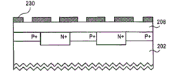
Fig. 2 A shows according to an embodiment of the invention corresponding to the sectional view operation 102 from flow process Figure 100, that be furnished with the substrate of dielectric layer thereon.The operation 102 of reference flowchart Figure 100 and corresponding Fig. 2 A, provide the substrate that is furnished with dielectric layer thereon.
With reference to figure 2A, substrate 200 has optical receiving surface 202 and the back side 204.In one embodiment, optical receiving surface 202 is by veining (as shown in Figure 2 A), to reduce less desirable reflection during solar radiation collection efficiency.In one embodiment, antireflecting coating 220 is formed on the optical receiving surface 202 of substrate 200 and is conformal with it.204 places, the back side at substrate 200 form a plurality of active areas 206.According to one embodiment of present invention, a plurality of active area 206 comprises alternately HeP+ district, N+ district (as shown in Figure 2 A).In one embodiment, substrate 200 comprises that crystalline silicon ,N+ district comprises that phosphorus dopant foreign atom ErP+ district comprises boron dope agent foreign atom.On the back side 204 of substrate 200, arrange dielectric layer 208.In one embodiment, dielectric layer 208 comprises the material such as silicon dioxide, but is not limited thereto.In another embodiment, dielectric layer 208 is stack of dielectric layers, and for example, dielectric layer 208 is included in the silicon dioxide layer of arranging on substrate 200 and the silicon nitride layer of arranging on this silicon dioxide layer.
Fig. 2 B shows according to an embodiment of the invention corresponding to the sectional view operation 104 from flow process Figure 100, that be formed with the substrate of free of pinholes mask layer thereon.The operation 104 of reference flowchart Figure 100 and corresponding Fig. 2 B form free of pinholes mask layer on dielectric layer.
With reference to figure 2B, on the surface of dielectric layer 208, form free of pinholes mask layer 210.The technology that can not form by being suitable for providing the conformal covering of dielectric layer 208 pin hole forms free of pinholes mask layer 210.According to one embodiment of present invention, form free of pinholes mask layer 210 and comprise use chemical vapor deposition technology.In one embodiment, use chemical vapor deposition technology to comprise the material of deposition such as amorphous silicon, amorphous carbon or polyimides, but be not limited thereto.In a particular embodiment, free of pinholes mask layer 210 comprises amorphous silicon, and by using such as silane (SiH
4) or disilane (Si
2h
6) and so on the chemical vapor deposition of gas form free of pinholes mask layer 210, but be not limited thereto.In another specific embodiment, free of pinholes mask layer 210 comprises amorphous carbon, and by using such as methane (CH
4), ethane (C
2h
6), propane (C
3h
8), the rare (C of second
2h
4) or propylene (C
3h
6) and so on the chemical vapor deposition of gas form free of pinholes mask layer 210, but be not limited thereto.For make efficiency, can in the identical processing operation with dielectric layer 208 depositions, deposit free of pinholes mask layer 210.For example, in one embodiment, dielectric layer 208 is the stack of dielectric layers that comprises silicon nitride layer, and by arrangement, is used in the order of the deposition gases in chemical vapor deposition processing, in the process cavity identical with silicon nitride layer and in identical treatment step, deposits free of pinholes mask layer 210.In another embodiment, formation free of pinholes mask layer 210 is included in separated processing operation and forms amorphous silicon layer on silicon dioxide dielectric layer 208.
Fig. 2 C shows the sectional view of the substrate corresponding to the free of pinholes mask layer operation 106 from flow process Figure 100, that be formed with patterning thereon according to an embodiment of the invention.The operation 106 of reference flowchart Figure 100 and corresponding Fig. 2 C, do not used mask, and free of pinholes mask layer is carried out to patterning, to form the free of pinholes mask layer of patterning.
With reference to figure 2C, the free of pinholes mask layer 210 on dielectric layer 208 is carried out to patterning, to form the free of pinholes mask layer 230 of patterning.In one embodiment, the pattern of the free of pinholes mask layer 230 of patterning has been determined and will be formed on the position of a plurality of contact openings in dielectric layer 208 subsequently.The technology that can not affect significantly by being suitable for selectively free of pinholes mask layer 210 being carried out to patterning dielectric layer 208 carries out to free of pinholes mask layer 210 the free of pinholes mask layer 230 that patterning forms patterning.According to one embodiment of present invention, free of pinholes mask layer 210 is carried out to patterning and comprise that to form the free of pinholes mask layer 230 of patterning use utilizes the laser ablation technology of laser.In one embodiment, use laser ablation technology to comprise to select to make free of pinholes mask layer 210 to have than dielectric layer 208 optical maser wavelength of ablation velocity faster.In a particular embodiment; during laser ablation; dielectric layer 208 protective substrates 200; this is because the band gap of dielectric layer 208 is greater than the band gap of substrate 200; otherwise in the situation that there is no dielectric layer 208, substrate 200 affects the laser ablation process that is undesirably used to free of pinholes mask layer 210 to carry out patterning.
According to another embodiment of the present invention, free of pinholes mask layer 210 is carried out to patterning and comprise a use point etching technique to form the free of pinholes mask layer 230 of patterning.In one embodiment, use a some etching technique to comprise to select to make free of pinholes mask layer 210 to have than dielectric layer 208 Wet-etching agent of etch-rate faster.In a particular embodiment, select Wet-etching agent to comprise the aqueous solution that uses potassium hydroxide.In a specific embodiment; at a during etching; dielectric layer 208 protective substrates 200; this be because the etch-rate of dielectric layer 208 far below the etch-rate of substrate 200; otherwise in the situation that there is no dielectric layer 208, substrate 200 affects the some etching that is undesirably used to the free of pinholes mask layer 210 to carry out patterning.Note, because the thickness dielectric layer 208 with respect to free of pinholes mask layer 210 has sizable thickness, so direct some etching of dielectric layer 208 may be invalid.Thereby according to one embodiment of present invention, when making a plurality of hard contact for solar cell, it is favourable using the free of pinholes mask layer of direct patterning to carry out patterning to dielectric layer.In one embodiment, the thickness of dielectric layer 208 is in the scope of about 100-500 nanometer, and the thickness of free of pinholes mask layer 210 is in the scope of about 1-100 nanometer.In one embodiment, the patterning of free of pinholes mask layer 210 retains whole dielectric layer 208 during being included in patterning.
Therefore, as described in conjunction with Fig. 2 A-2C, in the situation that not using mask, can carry out patterning to free of pinholes mask layer, to form the free of pinholes mask layer of patterning.After having formed free of pinholes mask layer, can make the hard contact of back contact solar cells, as described in conjunction with 2D-2F.
Fig. 2 D shows the sectional view of the substrate of the free of pinholes mask layer corresponding to the dielectric layer operation 108 from flow process Figure 100, that be formed with patterning thereon and patterning according to an embodiment of the invention.The operation 108 of reference flowchart Figure 100 and corresponding Fig. 2 D, used the free of pinholes mask layer of patterning, as mask, dielectric layer is carried out to etching, to form the dielectric layer of patterning and to expose the part of substrate.
With reference to figure 2D, by using the free of pinholes mask layer 230 of patterning as mask, in dielectric layer 208, form a plurality of contact openings, to form the dielectric layer 240 of patterning.Can from the free of pinholes mask layer 230 of patterning, shift patterns and (for example can not affect significantly by being suitable for selectively, etching) technology of the back side 204 of substrate 200 (that is, can not make the effect of a plurality of active areas 206 reduce) carries out to dielectric layer 208 dielectric layer 240 that patterning forms patterning.According to one embodiment of present invention, by using overall buffered oxide etch agent, dielectric layer 208 (is for example carried out to etching, by substrate 200 is immersed in buffered oxide etch agent), dielectric layer 208 is carried out to patterning to form the dielectric layer 240 of patterning.In one embodiment, buffered oxide etch agent comprises and includes hydrofluoric acid (HF) and ammonium fluoride (NH
4f) the aqueous solution.In a particular embodiment, HF: NH
4f ratio is about 1: 4-1: in 10 scope, and at the temperature within the scope of about 30-40 degree Celsius, in the scope that schedules to last about 3-10 minute, buffered oxide etch agent is applied to dielectric layer 208.
Fig. 2 E shows the sectional view of the substrate corresponding to the dielectric layer operation 110 from flow process Figure 100, that be formed with patterning thereon according to an embodiment of the invention, has wherein removed the free of pinholes mask layer of patterning.The operation 110 of reference flowchart Figure 100 and corresponding Fig. 2 E, the free of pinholes mask layer of removal patterning, with the dielectric layer of exposure pattern.
With reference to figure 2E, remove selectively the free of pinholes mask layer 230 of patterning, so that the dielectric layer 240 of the patterning that is formed with therein a plurality of openings to be provided.According to one embodiment of present invention, can by be suitable for keeping patterning dielectric layer 240 pattern integrity and (for example can not affect significantly, etching) technology of the back side 204 of substrate 200 (that is, can not make the effect of a plurality of active areas 206 reduce) is removed the free of pinholes mask layer 230 of patterning selectively.In one embodiment, the free of pinholes mask layer 230 of removal patterning comprises the aqueous solution that uses potassium hydroxide.
Fig. 2 F shows according to an embodiment of the invention corresponding to the sectional view operation 112 from flow process Figure 100, that be formed with the substrate of a plurality of hard contacts thereon.The operation 112 of reference flowchart Figure 100 and corresponding Fig. 2 F form a plurality of hard contacts in the dielectric layer of patterning.
With reference to figure 2F, by deposition the metallic material of patterning bag among the dielectric layer 240 at patterning and a plurality of active areas 206, form a plurality of hard contacts 250.In one embodiment, the metallic material of bag that is used to form a plurality of hard contacts 250 comprises the metal such as aluminium, silver, palladium or its alloy, but is not limited thereto.According to one embodiment of present invention, thus form back contact solar cells 260.
Therefore, disclose for making the method for solar cell.According to one embodiment of present invention, provide the substrate that is furnished with dielectric layer thereon.On this substrate, form free of pinholes mask layer.In the situation that not using mask, this free of pinholes mask layer is carried out to patterning, to form the free of pinholes mask layer of patterning.In one embodiment, during patterning, dielectric layer protective substrate.
Claims (21)
1. for making a method for solar cell, comprising:
The substrate that is furnished with dielectric layer is thereon provided;
On described dielectric layer, form free of pinholes mask layer;
In the situation that not using mask, described free of pinholes mask layer is carried out to patterning, to form the free of pinholes mask layer of patterning, wherein, during patterning, described dielectric layer is protected described substrate;
Use the free of pinholes mask layer of described patterning, as mask, described dielectric layer is carried out to etching, to form the dielectric layer of patterning and to expose the part of described substrate;
Remove the free of pinholes mask layer of described patterning, to expose the dielectric layer of described patterning; And
In the dielectric layer of described patterning, form a plurality of hard contacts.
2. according to the process of claim 1 wherein that described free of pinholes mask layer is carried out to patterning comprises the laser ablation technology that uses utilization to have the laser of certain wavelength.
3. according to the method for claim 2, wherein use laser ablation technology to comprise to select to make described free of pinholes mask layer to have than the described dielectric layer optical maser wavelength of ablation velocity faster.
4. according to the process of claim 1 wherein that described free of pinholes mask layer is carried out to patterning comprises that use utilizes the some etching technique of Wet-etching agent.
5. according to the method for claim 4, wherein use a some etching technique to comprise to select to make described free of pinholes mask layer to have than the described dielectric layer Wet-etching agent of etch-rate faster.
6. according to the method for claim 5, wherein select Wet-etching agent to comprise the aqueous solution that uses potassium hydroxide.
7. according to the process of claim 1 wherein that forming described free of pinholes mask layer comprises use chemical vapor deposition technology.
8. according to the method for claim 7, wherein use chemical vapor deposition technology to comprise and deposit the material in the group of selecting freely following material formation: amorphous silicon, amorphous carbon and polyimides.
9. according to the process of claim 1 wherein that providing the substrate with dielectric layer to comprise provides the crystalline silicon substrates that is furnished with silicon dioxide layer thereon, and wherein form described free of pinholes mask layer and be included on described silicon dioxide layer and form amorphous silicon layer.
10. according to the process of claim 1 wherein, described free of pinholes mask layer is carried out to the described dielectric layer that patterning comprises that reservation is whole.
11. 1 kinds for making the method for solar cell, comprising:
The substrate that is furnished with dielectric stack is thereon provided;
On described dielectric stack, form free of pinholes mask layer;
In the situation that not using mask, described free of pinholes mask layer is carried out to patterning, to form the free of pinholes mask layer of patterning, wherein, during patterning, described dielectric stack is protected described substrate;
Use the free of pinholes mask layer of described patterning, as mask, described dielectric stack is carried out to etching, to form the dielectric stack of patterning and to expose the part of described substrate;
Remove the free of pinholes mask layer of described patterning, to expose the dielectric stack of described patterning; And
In the dielectric stack of described patterning, form a plurality of hard contacts.
12. according to the method for claim 11, wherein described dielectric stack is carried out to the buffered oxide etch agent that etching comprises that use is overall.
13. according to the method for claim 11, and the free of pinholes mask layer of wherein removing described patterning comprises the aqueous solution that uses potassium hydroxide.
14. according to the method for claim 11, wherein described free of pinholes mask layer is carried out to patterning and comprise the laser ablation technology that use to utilize the laser with certain wavelength, and wherein use laser ablation technology to comprise to select to make described free of pinholes mask layer to have than the described dielectric stack layers optical maser wavelength of ablation velocity faster.
15. according to the method for claim 11, wherein described free of pinholes mask layer is carried out to patterning and comprise and use the some etching technique utilize Wet-etching agent, and wherein use a some etching technique to comprise to select to make described free of pinholes mask layer to have than the described dielectric stack Wet-etching agent of etch-rate faster.
16. according to the method for claim 15, wherein selects Wet-etching agent to comprise the aqueous solution that uses potassium hydroxide.
17. according to the method for claim 11, wherein forms described free of pinholes mask layer and comprises use chemical vapor deposition technology.
18. according to the method for claim 17, wherein uses chemical vapor deposition technology to comprise and deposits the material in the group of selecting freely following material formation: amorphous silicon, amorphous carbon and polyimides.
19. according to the method for claim 11, wherein provide the substrate with dielectric stack to comprise the crystalline silicon substrates that is furnished with silicon dioxide layer and is furnished with silicon nitride layer on this substrate on this silicon dioxide layer is provided, and wherein form described free of pinholes mask layer and be included on described silicon nitride layer and form amorphous silicon layer.
20. according to the method for claim 11, wherein described free of pinholes mask layer is carried out to the described dielectric stack that patterning comprises that reservation is whole.
21. 1 kinds of solar cells that use is manufactured according to the method described in any one in claim 1 to 20.
Applications Claiming Priority (3)
| Application Number | Priority Date | Filing Date | Title |
|---|---|---|---|
| US12/233,819 | 2008-09-19 | ||
| US12/233,819 US20100071765A1 (en) | 2008-09-19 | 2008-09-19 | Method for fabricating a solar cell using a direct-pattern pin-hole-free masking layer |
| PCT/US2009/050960 WO2010033296A1 (en) | 2008-09-19 | 2009-07-17 | Method for fabricating a solar cell using a direct-pattern pin-hole-free masking layer |
Publications (2)
| Publication Number | Publication Date |
|---|---|
| CN102160192A CN102160192A (en) | 2011-08-17 |
| CN102160192B true CN102160192B (en) | 2014-03-12 |
Family
ID=42036391
Family Applications (1)
| Application Number | Title | Priority Date | Filing Date |
|---|---|---|---|
| CN200980136212.XA Expired - Fee Related CN102160192B (en) | 2008-09-19 | 2009-07-17 | Method for fabricating solar cell using direct-pattern pin-hole-free masking layer |
Country Status (6)
| Country | Link |
|---|---|
| US (1) | US20100071765A1 (en) |
| EP (1) | EP2329529A4 (en) |
| JP (2) | JP2012503330A (en) |
| KR (1) | KR20110063546A (en) |
| CN (1) | CN102160192B (en) |
| WO (1) | WO2010033296A1 (en) |
Families Citing this family (16)
| Publication number | Priority date | Publication date | Assignee | Title |
|---|---|---|---|---|
| US8324015B2 (en) * | 2009-12-01 | 2012-12-04 | Sunpower Corporation | Solar cell contact formation using laser ablation |
| US8211731B2 (en) * | 2010-06-07 | 2012-07-03 | Sunpower Corporation | Ablation of film stacks in solar cell fabrication processes |
| US8586403B2 (en) | 2011-02-15 | 2013-11-19 | Sunpower Corporation | Process and structures for fabrication of solar cells with laser ablation steps to form contact holes |
| US20140166094A1 (en) * | 2012-12-18 | 2014-06-19 | Paul Loscutoff | Solar cell emitter region fabrication using etch resistant film |
| US8916038B2 (en) | 2013-03-13 | 2014-12-23 | Gtat Corporation | Free-standing metallic article for semiconductors |
| US8936709B2 (en) | 2013-03-13 | 2015-01-20 | Gtat Corporation | Adaptable free-standing metallic article for semiconductors |
| TWI631724B (en) * | 2013-03-13 | 2018-08-01 | 美商梅林太陽能科技股份有限公司 | Method of forming a photovoltaic cell |
| US8569096B1 (en) * | 2013-03-13 | 2013-10-29 | Gtat Corporation | Free-standing metallic article for semiconductors |
| WO2014144967A1 (en) * | 2013-03-15 | 2014-09-18 | Sunpower Corporation | Reduced contact resistance and improved lifetime of solar cells |
| WO2015159456A1 (en) * | 2014-04-16 | 2015-10-22 | 三菱電機株式会社 | Solar cell and solar cell manufacturing method |
| US9461192B2 (en) | 2014-12-16 | 2016-10-04 | Sunpower Corporation | Thick damage buffer for foil-based metallization of solar cells |
| CN107408599B (en) * | 2015-03-24 | 2020-11-27 | 松下知识产权经营株式会社 | Method for manufacturing solar cell |
| WO2016158226A1 (en) * | 2015-03-31 | 2016-10-06 | 株式会社カネカ | Solar cell and method for manufacturing same |
| US20160380127A1 (en) * | 2015-06-26 | 2016-12-29 | Richard Hamilton SEWELL | Leave-In Etch Mask for Foil-Based Metallization of Solar Cells |
| CN117374169B (en) * | 2023-12-07 | 2024-03-12 | 浙江晶科能源有限公司 | Preparation method of back contact solar cell and back contact solar cell |
| CN117673207A (en) * | 2024-02-01 | 2024-03-08 | 通威太阳能(眉山)有限公司 | Preparation method of solar cell, solar cell and photovoltaic module |
Family Cites Families (29)
| Publication number | Priority date | Publication date | Assignee | Title |
|---|---|---|---|---|
| US4353778A (en) * | 1981-09-04 | 1982-10-12 | International Business Machines Corporation | Method of etching polyimide |
| JPS6215864A (en) * | 1985-07-15 | 1987-01-24 | Hitachi Ltd | Manufacture of solar cell |
| US5041361A (en) * | 1988-08-08 | 1991-08-20 | Midwest Research Institute | Oxygen ion-beam microlithography |
| JPH03285332A (en) * | 1990-04-02 | 1991-12-16 | Ricoh Co Ltd | Masking film |
| JPH046121A (en) * | 1990-04-23 | 1992-01-10 | Shin Etsu Chem Co Ltd | Production of glass preform for optical fiber |
| JP2986875B2 (en) * | 1990-09-07 | 1999-12-06 | キヤノン株式会社 | Integrated solar cell |
| WO1993018545A1 (en) * | 1992-03-10 | 1993-09-16 | Lasa Industries Inc. | Method of laser etching of silicon dioxide |
| US5759745A (en) * | 1995-12-05 | 1998-06-02 | Materials Research Group, Inc. | Method of using amorphous silicon as a photoresist |
| JP2005167291A (en) * | 1996-12-20 | 2005-06-23 | Mitsubishi Electric Corp | Solar cell manufacturing method and semiconductor device manufacturing method |
| WO1999031514A1 (en) * | 1997-12-15 | 1999-06-24 | Seiko Instruments Inc. | Optical waveguide probe and its manufacturing method |
| JPH11220101A (en) * | 1998-01-30 | 1999-08-10 | Matsushita Electric Ind Co Ltd | Semiconductor device and its manufacture |
| JP5121090B2 (en) * | 2000-02-17 | 2013-01-16 | アプライド マテリアルズ インコーポレイテッド | Method for depositing amorphous carbon layer |
| US6696008B2 (en) * | 2000-05-25 | 2004-02-24 | Westar Photonics Inc. | Maskless laser beam patterning ablation of multilayered structures with continuous monitoring of ablation |
| US20020173157A1 (en) * | 2001-03-29 | 2002-11-21 | Taiwan Semiconductor Manufacturing Co., Ltd. | Dual damascene method employing composite low dielectric constant dielectric layer having intrinsic etch stop characteristics |
| EP1378947A1 (en) * | 2002-07-01 | 2004-01-07 | Interuniversitair Microelektronica Centrum Vzw | Semiconductor etching paste and the use thereof for localised etching of semiconductor substrates |
| US7388147B2 (en) * | 2003-04-10 | 2008-06-17 | Sunpower Corporation | Metal contact structure for solar cell and method of manufacture |
| US7122392B2 (en) * | 2003-06-30 | 2006-10-17 | Intel Corporation | Methods of forming a high germanium concentration silicon germanium alloy by epitaxial lateral overgrowth and structures formed thereby |
| JP2005136062A (en) * | 2003-10-29 | 2005-05-26 | Sharp Corp | Manufacturing method of solar battery |
| US20050151129A1 (en) * | 2004-01-14 | 2005-07-14 | Rahul Gupta | Deposition of conducting polymers |
| JP2006080450A (en) * | 2004-09-13 | 2006-03-23 | Sharp Corp | Solar battery manufacturing method |
| DE102004050269A1 (en) * | 2004-10-14 | 2006-04-20 | Institut Für Solarenergieforschung Gmbh | Process for the contact separation of electrically conductive layers on back-contacted solar cells and solar cell |
| EP1763086A1 (en) * | 2005-09-09 | 2007-03-14 | Interuniversitair Micro-Elektronica Centrum | Photovoltaic cell with thick silicon oxide and silicon nitride passivation and fabrication method |
| US7737357B2 (en) * | 2006-05-04 | 2010-06-15 | Sunpower Corporation | Solar cell having doped semiconductor heterojunction contacts |
| GB0612754D0 (en) * | 2006-06-27 | 2006-08-09 | Univ Cambridge Tech | Semiconductor device transducer and method |
| JP5329784B2 (en) * | 2006-08-25 | 2013-10-30 | 株式会社半導体エネルギー研究所 | Method for manufacturing semiconductor device |
| KR101241617B1 (en) * | 2006-12-01 | 2013-03-08 | 샤프 가부시키가이샤 | Solar cell and method of manufacturing the same |
| JP4630294B2 (en) * | 2007-01-29 | 2011-02-09 | シャープ株式会社 | Photoelectric conversion device and manufacturing method thereof |
| US20080314443A1 (en) * | 2007-06-23 | 2008-12-25 | Christopher Michael Bonner | Back-contact solar cell for high power-over-weight applications |
| US7517709B1 (en) * | 2007-11-16 | 2009-04-14 | Applied Materials, Inc. | Method of forming backside point contact structures for silicon solar cells |
-
2008
- 2008-09-19 US US12/233,819 patent/US20100071765A1/en not_active Abandoned
-
2009
- 2009-07-17 JP JP2011527849A patent/JP2012503330A/en active Pending
- 2009-07-17 WO PCT/US2009/050960 patent/WO2010033296A1/en active Application Filing
- 2009-07-17 KR KR1020117008770A patent/KR20110063546A/en not_active Application Discontinuation
- 2009-07-17 CN CN200980136212.XA patent/CN102160192B/en not_active Expired - Fee Related
- 2009-07-17 EP EP09814940.4A patent/EP2329529A4/en not_active Withdrawn
-
2013
- 2013-11-13 JP JP2013235039A patent/JP2014060430A/en active Pending
Also Published As
| Publication number | Publication date |
|---|---|
| KR20110063546A (en) | 2011-06-10 |
| EP2329529A1 (en) | 2011-06-08 |
| JP2012503330A (en) | 2012-02-02 |
| CN102160192A (en) | 2011-08-17 |
| US20100071765A1 (en) | 2010-03-25 |
| EP2329529A4 (en) | 2017-10-11 |
| WO2010033296A1 (en) | 2010-03-25 |
| JP2014060430A (en) | 2014-04-03 |
Similar Documents
| Publication | Publication Date | Title |
|---|---|---|
| CN102160192B (en) | Method for fabricating solar cell using direct-pattern pin-hole-free masking layer | |
| US7670638B2 (en) | Protection layer for fabricating a solar cell | |
| JP2020129689A (en) | Solar cell | |
| JP6178400B2 (en) | Solar cell having an emitter region containing a wide bandgap semiconductor material | |
| JP5863391B2 (en) | Method for manufacturing crystalline silicon solar cell | |
| TW201528344A (en) | Solar cell emitter region fabrication using ion implantation | |
| JP2004531074A (en) | Solar cell manufacturing method | |
| EP2782146A1 (en) | Solar cell with reduced potential induced degradation and manufacturing method thereof | |
| EP2782144A1 (en) | Method for fabricating heterojunction interdigitated back contact photovoltaic cells | |
| CN105308755A (en) | Epitaxial silicon solar cells with moisture barrier | |
| JP4827550B2 (en) | Manufacturing method of solar cell | |
| CN115188837B (en) | Back contact solar cell, preparation method and cell assembly | |
| JP2006156646A (en) | Solar cell manufacturing method | |
| CN108713255A (en) | Solar cell device | |
| CN114914328B (en) | Double-sided solar cell and preparation method thereof | |
| CN101312219A (en) | Solar battery | |
| TW201937748A (en) | Method for producing solar cell | |
| CN114005907A (en) | Manufacturing method of Topcon battery | |
| JP5172993B2 (en) | Method for forming texture structure and method for manufacturing solar cell | |
| KR101154095B1 (en) | Solar cell and manufacturing method of the same | |
| CN101312222A (en) | Method of manufacturing solar cell | |
| CN110957396A (en) | Zero-bias working graphene photoelectric device and preparation method thereof | |
| CN114664954A (en) | Manufacturing method of passivated back contact solar cell |
Legal Events
| Date | Code | Title | Description |
|---|---|---|---|
| C06 | Publication | ||
| PB01 | Publication | ||
| C10 | Entry into substantive examination | ||
| SE01 | Entry into force of request for substantive examination | ||
| GR01 | Patent grant | ||
| GR01 | Patent grant | ||
| CF01 | Termination of patent right due to non-payment of annual fee | ||
| CF01 | Termination of patent right due to non-payment of annual fee |
Granted publication date: 20140312 Termination date: 20170717 |