JP2005167291A - Solar cell manufacturing method and semiconductor device manufacturing method - Google Patents
Solar cell manufacturing method and semiconductor device manufacturing method Download PDFInfo
- Publication number
- JP2005167291A JP2005167291A JP2005069769A JP2005069769A JP2005167291A JP 2005167291 A JP2005167291 A JP 2005167291A JP 2005069769 A JP2005069769 A JP 2005069769A JP 2005069769 A JP2005069769 A JP 2005069769A JP 2005167291 A JP2005167291 A JP 2005167291A
- Authority
- JP
- Japan
- Prior art keywords
- electrode
- manufacturing
- silicon
- glass
- solar cell
- Prior art date
- Legal status (The legal status is an assumption and is not a legal conclusion. Google has not performed a legal analysis and makes no representation as to the accuracy of the status listed.)
- Pending
Links
- 238000004519 manufacturing process Methods 0.000 title claims abstract description 90
- 239000004065 semiconductor Substances 0.000 title claims abstract description 85
- 238000000034 method Methods 0.000 claims abstract description 153
- 239000011521 glass Substances 0.000 claims abstract description 115
- 239000000758 substrate Substances 0.000 claims abstract description 96
- 229910052710 silicon Inorganic materials 0.000 claims abstract description 74
- 239000010703 silicon Substances 0.000 claims abstract description 71
- 229910052581 Si3N4 Inorganic materials 0.000 claims abstract description 61
- HQVNEWCFYHHQES-UHFFFAOYSA-N silicon nitride Chemical compound N12[Si]34N5[Si]62N3[Si]51N64 HQVNEWCFYHHQES-UHFFFAOYSA-N 0.000 claims abstract description 60
- 239000000463 material Substances 0.000 claims abstract description 59
- GWEVSGVZZGPLCZ-UHFFFAOYSA-N Titan oxide Chemical compound O=[Ti]=O GWEVSGVZZGPLCZ-UHFFFAOYSA-N 0.000 claims abstract description 32
- OGIDPMRJRNCKJF-UHFFFAOYSA-N titanium oxide Inorganic materials [Ti]=O OGIDPMRJRNCKJF-UHFFFAOYSA-N 0.000 claims abstract description 32
- 229910052751 metal Inorganic materials 0.000 claims abstract description 23
- 239000002184 metal Substances 0.000 claims abstract description 23
- 229910052782 aluminium Inorganic materials 0.000 claims abstract description 22
- XAGFODPZIPBFFR-UHFFFAOYSA-N aluminium Chemical compound [Al] XAGFODPZIPBFFR-UHFFFAOYSA-N 0.000 claims abstract description 22
- -1 aluminum silver Chemical compound 0.000 claims abstract description 20
- 239000010408 film Substances 0.000 claims description 191
- 239000010410 layer Substances 0.000 claims description 131
- XUIMIQQOPSSXEZ-UHFFFAOYSA-N Silicon Chemical compound [Si] XUIMIQQOPSSXEZ-UHFFFAOYSA-N 0.000 claims description 70
- 238000010304 firing Methods 0.000 claims description 59
- BQCADISMDOOEFD-UHFFFAOYSA-N Silver Chemical compound [Ag] BQCADISMDOOEFD-UHFFFAOYSA-N 0.000 claims description 38
- 229910052709 silver Inorganic materials 0.000 claims description 38
- 239000004332 silver Substances 0.000 claims description 38
- KRHYYFGTRYWZRS-UHFFFAOYSA-N Fluorane Chemical compound F KRHYYFGTRYWZRS-UHFFFAOYSA-N 0.000 claims description 32
- VYPSYNLAJGMNEJ-UHFFFAOYSA-N Silicium dioxide Chemical compound O=[Si]=O VYPSYNLAJGMNEJ-UHFFFAOYSA-N 0.000 claims description 29
- 229910052814 silicon oxide Inorganic materials 0.000 claims description 29
- 239000007789 gas Substances 0.000 claims description 22
- 238000005268 plasma chemical vapour deposition Methods 0.000 claims description 14
- 238000002230 thermal chemical vapour deposition Methods 0.000 claims description 14
- QVGXLLKOCUKJST-UHFFFAOYSA-N atomic oxygen Chemical compound [O] QVGXLLKOCUKJST-UHFFFAOYSA-N 0.000 claims description 13
- 229910052760 oxygen Inorganic materials 0.000 claims description 12
- 239000001301 oxygen Substances 0.000 claims description 12
- 239000007864 aqueous solution Substances 0.000 claims description 10
- 238000002844 melting Methods 0.000 claims description 10
- 230000008018 melting Effects 0.000 claims description 10
- ZOXJGFHDIHLPTG-UHFFFAOYSA-N Boron Chemical compound [B] ZOXJGFHDIHLPTG-UHFFFAOYSA-N 0.000 claims description 9
- 229910052796 boron Inorganic materials 0.000 claims description 9
- UFHFLCQGNIYNRP-UHFFFAOYSA-N Hydrogen Chemical compound [H][H] UFHFLCQGNIYNRP-UHFFFAOYSA-N 0.000 claims description 8
- 239000010409 thin film Substances 0.000 claims description 8
- IJGRMHOSHXDMSA-UHFFFAOYSA-N Atomic nitrogen Chemical compound N#N IJGRMHOSHXDMSA-UHFFFAOYSA-N 0.000 claims description 7
- 229910052739 hydrogen Inorganic materials 0.000 claims description 7
- 239000001257 hydrogen Substances 0.000 claims description 7
- 238000010438 heat treatment Methods 0.000 claims description 6
- 229910052757 nitrogen Inorganic materials 0.000 claims description 6
- 239000002356 single layer Substances 0.000 claims description 5
- DDFHBQSCUXNBSA-UHFFFAOYSA-N 5-(5-carboxythiophen-2-yl)thiophene-2-carboxylic acid Chemical compound S1C(C(=O)O)=CC=C1C1=CC=C(C(O)=O)S1 DDFHBQSCUXNBSA-UHFFFAOYSA-N 0.000 claims description 4
- RTAQQCXQSZGOHL-UHFFFAOYSA-N Titanium Chemical compound [Ti] RTAQQCXQSZGOHL-UHFFFAOYSA-N 0.000 claims description 4
- 230000003647 oxidation Effects 0.000 claims description 4
- 238000007254 oxidation reaction Methods 0.000 claims description 4
- 230000000149 penetrating effect Effects 0.000 claims description 4
- 239000011344 liquid material Substances 0.000 claims description 3
- 238000010248 power generation Methods 0.000 claims description 3
- 229910052719 titanium Inorganic materials 0.000 claims description 3
- 239000010936 titanium Substances 0.000 claims description 3
- 238000009792 diffusion process Methods 0.000 abstract description 86
- 238000000926 separation method Methods 0.000 abstract description 16
- 238000005245 sintering Methods 0.000 abstract 2
- 230000008569 process Effects 0.000 description 52
- 230000000694 effects Effects 0.000 description 36
- 230000015572 biosynthetic process Effects 0.000 description 28
- OAICVXFJPJFONN-UHFFFAOYSA-N Phosphorus Chemical compound [P] OAICVXFJPJFONN-UHFFFAOYSA-N 0.000 description 16
- 229910052698 phosphorus Inorganic materials 0.000 description 16
- 239000011574 phosphorus Substances 0.000 description 16
- 239000012535 impurity Substances 0.000 description 13
- 238000007639 printing Methods 0.000 description 13
- BLRPTPMANUNPDV-UHFFFAOYSA-N Silane Chemical compound [SiH4] BLRPTPMANUNPDV-UHFFFAOYSA-N 0.000 description 11
- 239000000203 mixture Substances 0.000 description 11
- 238000007650 screen-printing Methods 0.000 description 11
- QGZKDVFQNNGYKY-UHFFFAOYSA-N Ammonia Chemical compound N QGZKDVFQNNGYKY-UHFFFAOYSA-N 0.000 description 10
- 238000006243 chemical reaction Methods 0.000 description 10
- XHXFXVLFKHQFAL-UHFFFAOYSA-N phosphoryl trichloride Chemical compound ClP(Cl)(Cl)=O XHXFXVLFKHQFAL-UHFFFAOYSA-N 0.000 description 10
- HEMHJVSKTPXQMS-UHFFFAOYSA-M Sodium hydroxide Chemical compound [OH-].[Na+] HEMHJVSKTPXQMS-UHFFFAOYSA-M 0.000 description 9
- 238000005530 etching Methods 0.000 description 9
- 238000000059 patterning Methods 0.000 description 9
- 238000010586 diagram Methods 0.000 description 7
- 238000005468 ion implantation Methods 0.000 description 7
- 238000002955 isolation Methods 0.000 description 7
- 238000001035 drying Methods 0.000 description 6
- 230000003628 erosive effect Effects 0.000 description 6
- 230000000737 periodic effect Effects 0.000 description 6
- RLOWWWKZYUNIDI-UHFFFAOYSA-N phosphinic chloride Chemical compound ClP=O RLOWWWKZYUNIDI-UHFFFAOYSA-N 0.000 description 6
- 239000013078 crystal Substances 0.000 description 5
- 239000007772 electrode material Substances 0.000 description 5
- 238000002474 experimental method Methods 0.000 description 5
- 238000007654 immersion Methods 0.000 description 5
- 230000008859 change Effects 0.000 description 4
- 238000005229 chemical vapour deposition Methods 0.000 description 4
- VNWKTOKETHGBQD-UHFFFAOYSA-N methane Chemical compound C VNWKTOKETHGBQD-UHFFFAOYSA-N 0.000 description 4
- 229910000069 nitrogen hydride Inorganic materials 0.000 description 4
- 239000011295 pitch Substances 0.000 description 4
- FDNAPBUWERUEDA-UHFFFAOYSA-N silicon tetrachloride Chemical compound Cl[Si](Cl)(Cl)Cl FDNAPBUWERUEDA-UHFFFAOYSA-N 0.000 description 4
- 239000000243 solution Substances 0.000 description 4
- LYCAIKOWRPUZTN-UHFFFAOYSA-N Ethylene glycol Chemical compound OCCO LYCAIKOWRPUZTN-UHFFFAOYSA-N 0.000 description 3
- KWYUFKZDYYNOTN-UHFFFAOYSA-M Potassium hydroxide Chemical compound [OH-].[K+] KWYUFKZDYYNOTN-UHFFFAOYSA-M 0.000 description 3
- 238000000137 annealing Methods 0.000 description 3
- 238000011109 contamination Methods 0.000 description 3
- 238000000354 decomposition reaction Methods 0.000 description 3
- 230000007547 defect Effects 0.000 description 3
- MROCJMGDEKINLD-UHFFFAOYSA-N dichlorosilane Chemical compound Cl[SiH2]Cl MROCJMGDEKINLD-UHFFFAOYSA-N 0.000 description 3
- MTHSVFCYNBDYFN-UHFFFAOYSA-N diethylene glycol Chemical compound OCCOCCO MTHSVFCYNBDYFN-UHFFFAOYSA-N 0.000 description 3
- 230000006872 improvement Effects 0.000 description 3
- 229910021420 polycrystalline silicon Inorganic materials 0.000 description 3
- 239000002994 raw material Substances 0.000 description 3
- 238000005215 recombination Methods 0.000 description 3
- 230000006798 recombination Effects 0.000 description 3
- 229910000077 silane Inorganic materials 0.000 description 3
- XNWFRZJHXBZDAG-UHFFFAOYSA-N 2-METHOXYETHANOL Chemical compound COCCO XNWFRZJHXBZDAG-UHFFFAOYSA-N 0.000 description 2
- OTMSDBZUPAUEDD-UHFFFAOYSA-N Ethane Chemical compound CC OTMSDBZUPAUEDD-UHFFFAOYSA-N 0.000 description 2
- VEXZGXHMUGYJMC-UHFFFAOYSA-N Hydrochloric acid Chemical compound Cl VEXZGXHMUGYJMC-UHFFFAOYSA-N 0.000 description 2
- MHAJPDPJQMAIIY-UHFFFAOYSA-N Hydrogen peroxide Chemical compound OO MHAJPDPJQMAIIY-UHFFFAOYSA-N 0.000 description 2
- XEEYBQQBJWHFJM-UHFFFAOYSA-N Iron Chemical compound [Fe] XEEYBQQBJWHFJM-UHFFFAOYSA-N 0.000 description 2
- 229910019213 POCl3 Inorganic materials 0.000 description 2
- XYFCBTPGUUZFHI-UHFFFAOYSA-N Phosphine Chemical compound P XYFCBTPGUUZFHI-UHFFFAOYSA-N 0.000 description 2
- 229910003910 SiCl4 Inorganic materials 0.000 description 2
- HAYXDMNJJFVXCI-UHFFFAOYSA-N arsenic(5+) Chemical compound [As+5] HAYXDMNJJFVXCI-UHFFFAOYSA-N 0.000 description 2
- 238000005266 casting Methods 0.000 description 2
- 238000007796 conventional method Methods 0.000 description 2
- 230000006378 damage Effects 0.000 description 2
- 230000007423 decrease Effects 0.000 description 2
- 229940028356 diethylene glycol monobutyl ether Drugs 0.000 description 2
- PZPGRFITIJYNEJ-UHFFFAOYSA-N disilane Chemical compound [SiH3][SiH3] PZPGRFITIJYNEJ-UHFFFAOYSA-N 0.000 description 2
- 238000011156 evaluation Methods 0.000 description 2
- 229910021480 group 4 element Inorganic materials 0.000 description 2
- 229910021478 group 5 element Inorganic materials 0.000 description 2
- 239000012212 insulator Substances 0.000 description 2
- 238000004518 low pressure chemical vapour deposition Methods 0.000 description 2
- 239000000155 melt Substances 0.000 description 2
- 239000011259 mixed solution Substances 0.000 description 2
- 238000002156 mixing Methods 0.000 description 2
- 229910021421 monocrystalline silicon Inorganic materials 0.000 description 2
- QPJSUIGXIBEQAC-UHFFFAOYSA-N n-(2,4-dichloro-5-propan-2-yloxyphenyl)acetamide Chemical compound CC(C)OC1=CC(NC(C)=O)=C(Cl)C=C1Cl QPJSUIGXIBEQAC-UHFFFAOYSA-N 0.000 description 2
- JCGNDDUYTRNOFT-UHFFFAOYSA-N oxolane-2,4-dione Chemical compound O=C1COC(=O)C1 JCGNDDUYTRNOFT-UHFFFAOYSA-N 0.000 description 2
- 230000007261 regionalization Effects 0.000 description 2
- 238000001004 secondary ion mass spectrometry Methods 0.000 description 2
- HBMJWWWQQXIZIP-UHFFFAOYSA-N silicon carbide Chemical compound [Si+]#[C-] HBMJWWWQQXIZIP-UHFFFAOYSA-N 0.000 description 2
- ZDHXKXAHOVTTAH-UHFFFAOYSA-N trichlorosilane Chemical compound Cl[SiH](Cl)Cl ZDHXKXAHOVTTAH-UHFFFAOYSA-N 0.000 description 2
- 239000005052 trichlorosilane Substances 0.000 description 2
- XLYOFNOQVPJJNP-UHFFFAOYSA-N water Substances O XLYOFNOQVPJJNP-UHFFFAOYSA-N 0.000 description 2
- GRYLNZFGIOXLOG-UHFFFAOYSA-N Nitric acid Chemical compound O[N+]([O-])=O GRYLNZFGIOXLOG-UHFFFAOYSA-N 0.000 description 1
- 229910004541 SiN Inorganic materials 0.000 description 1
- 229910004205 SiNX Inorganic materials 0.000 description 1
- 229910004298 SiO 2 Inorganic materials 0.000 description 1
- 229910010413 TiO 2 Inorganic materials 0.000 description 1
- 230000002411 adverse Effects 0.000 description 1
- 229910021529 ammonia Inorganic materials 0.000 description 1
- 229910052787 antimony Inorganic materials 0.000 description 1
- WATWJIUSRGPENY-UHFFFAOYSA-N antimony atom Chemical compound [Sb] WATWJIUSRGPENY-UHFFFAOYSA-N 0.000 description 1
- 229910052785 arsenic Inorganic materials 0.000 description 1
- RQNWIZPPADIBDY-UHFFFAOYSA-N arsenic atom Chemical compound [As] RQNWIZPPADIBDY-UHFFFAOYSA-N 0.000 description 1
- 229910052793 cadmium Inorganic materials 0.000 description 1
- BDOSMKKIYDKNTQ-UHFFFAOYSA-N cadmium atom Chemical compound [Cd] BDOSMKKIYDKNTQ-UHFFFAOYSA-N 0.000 description 1
- 239000000969 carrier Substances 0.000 description 1
- 230000015556 catabolic process Effects 0.000 description 1
- 238000003486 chemical etching Methods 0.000 description 1
- 238000004140 cleaning Methods 0.000 description 1
- 239000011248 coating agent Substances 0.000 description 1
- 238000000576 coating method Methods 0.000 description 1
- 239000000470 constituent Substances 0.000 description 1
- 238000003795 desorption Methods 0.000 description 1
- ZOCHARZZJNPSEU-UHFFFAOYSA-N diboron Chemical compound B#B ZOCHARZZJNPSEU-UHFFFAOYSA-N 0.000 description 1
- 229910001873 dinitrogen Inorganic materials 0.000 description 1
- 238000011038 discontinuous diafiltration by volume reduction Methods 0.000 description 1
- 239000002003 electrode paste Substances 0.000 description 1
- 229940093476 ethylene glycol Drugs 0.000 description 1
- 229910001385 heavy metal Inorganic materials 0.000 description 1
- 229910052742 iron Inorganic materials 0.000 description 1
- 239000007788 liquid Substances 0.000 description 1
- 230000007246 mechanism Effects 0.000 description 1
- 229910017604 nitric acid Inorganic materials 0.000 description 1
- 239000003960 organic solvent Substances 0.000 description 1
- 238000002161 passivation Methods 0.000 description 1
- 235000011837 pasties Nutrition 0.000 description 1
- 230000001737 promoting effect Effects 0.000 description 1
- 238000000197 pyrolysis Methods 0.000 description 1
- 230000009467 reduction Effects 0.000 description 1
- 238000004528 spin coating Methods 0.000 description 1
- 238000004544 sputter deposition Methods 0.000 description 1
- 230000003746 surface roughness Effects 0.000 description 1
- 230000009897 systematic effect Effects 0.000 description 1
- JBQYATWDVHIOAR-UHFFFAOYSA-N tellanylidenegermanium Chemical compound [Te]=[Ge] JBQYATWDVHIOAR-UHFFFAOYSA-N 0.000 description 1
- 238000005979 thermal decomposition reaction Methods 0.000 description 1
- 238000005406 washing Methods 0.000 description 1
Images


Classifications
-
- H—ELECTRICITY
- H01—ELECTRIC ELEMENTS
- H01L—SEMICONDUCTOR DEVICES NOT COVERED BY CLASS H10
- H01L31/00—Semiconductor devices sensitive to infrared radiation, light, electromagnetic radiation of shorter wavelength or corpuscular radiation and specially adapted either for the conversion of the energy of such radiation into electrical energy or for the control of electrical energy by such radiation; Processes or apparatus specially adapted for the manufacture or treatment thereof or of parts thereof; Details thereof
- H01L31/04—Semiconductor devices sensitive to infrared radiation, light, electromagnetic radiation of shorter wavelength or corpuscular radiation and specially adapted either for the conversion of the energy of such radiation into electrical energy or for the control of electrical energy by such radiation; Processes or apparatus specially adapted for the manufacture or treatment thereof or of parts thereof; Details thereof adapted as photovoltaic [PV] conversion devices
- H01L31/06—Semiconductor devices sensitive to infrared radiation, light, electromagnetic radiation of shorter wavelength or corpuscular radiation and specially adapted either for the conversion of the energy of such radiation into electrical energy or for the control of electrical energy by such radiation; Processes or apparatus specially adapted for the manufacture or treatment thereof or of parts thereof; Details thereof adapted as photovoltaic [PV] conversion devices characterised by at least one potential-jump barrier or surface barrier
- H01L31/068—Semiconductor devices sensitive to infrared radiation, light, electromagnetic radiation of shorter wavelength or corpuscular radiation and specially adapted either for the conversion of the energy of such radiation into electrical energy or for the control of electrical energy by such radiation; Processes or apparatus specially adapted for the manufacture or treatment thereof or of parts thereof; Details thereof adapted as photovoltaic [PV] conversion devices characterised by at least one potential-jump barrier or surface barrier the potential barriers being only of the PN homojunction type, e.g. bulk silicon PN homojunction solar cells or thin film polycrystalline silicon PN homojunction solar cells
-
- H—ELECTRICITY
- H01—ELECTRIC ELEMENTS
- H01L—SEMICONDUCTOR DEVICES NOT COVERED BY CLASS H10
- H01L31/00—Semiconductor devices sensitive to infrared radiation, light, electromagnetic radiation of shorter wavelength or corpuscular radiation and specially adapted either for the conversion of the energy of such radiation into electrical energy or for the control of electrical energy by such radiation; Processes or apparatus specially adapted for the manufacture or treatment thereof or of parts thereof; Details thereof
- H01L31/02—Details
- H01L31/0224—Electrodes
- H01L31/022408—Electrodes for devices characterised by at least one potential jump barrier or surface barrier
- H01L31/022425—Electrodes for devices characterised by at least one potential jump barrier or surface barrier for solar cells
- H01L31/022441—Electrode arrangements specially adapted for back-contact solar cells
-
- H—ELECTRICITY
- H01—ELECTRIC ELEMENTS
- H01L—SEMICONDUCTOR DEVICES NOT COVERED BY CLASS H10
- H01L31/00—Semiconductor devices sensitive to infrared radiation, light, electromagnetic radiation of shorter wavelength or corpuscular radiation and specially adapted either for the conversion of the energy of such radiation into electrical energy or for the control of electrical energy by such radiation; Processes or apparatus specially adapted for the manufacture or treatment thereof or of parts thereof; Details thereof
- H01L31/04—Semiconductor devices sensitive to infrared radiation, light, electromagnetic radiation of shorter wavelength or corpuscular radiation and specially adapted either for the conversion of the energy of such radiation into electrical energy or for the control of electrical energy by such radiation; Processes or apparatus specially adapted for the manufacture or treatment thereof or of parts thereof; Details thereof adapted as photovoltaic [PV] conversion devices
- H01L31/06—Semiconductor devices sensitive to infrared radiation, light, electromagnetic radiation of shorter wavelength or corpuscular radiation and specially adapted either for the conversion of the energy of such radiation into electrical energy or for the control of electrical energy by such radiation; Processes or apparatus specially adapted for the manufacture or treatment thereof or of parts thereof; Details thereof adapted as photovoltaic [PV] conversion devices characterised by at least one potential-jump barrier or surface barrier
- H01L31/068—Semiconductor devices sensitive to infrared radiation, light, electromagnetic radiation of shorter wavelength or corpuscular radiation and specially adapted either for the conversion of the energy of such radiation into electrical energy or for the control of electrical energy by such radiation; Processes or apparatus specially adapted for the manufacture or treatment thereof or of parts thereof; Details thereof adapted as photovoltaic [PV] conversion devices characterised by at least one potential-jump barrier or surface barrier the potential barriers being only of the PN homojunction type, e.g. bulk silicon PN homojunction solar cells or thin film polycrystalline silicon PN homojunction solar cells
- H01L31/0682—Semiconductor devices sensitive to infrared radiation, light, electromagnetic radiation of shorter wavelength or corpuscular radiation and specially adapted either for the conversion of the energy of such radiation into electrical energy or for the control of electrical energy by such radiation; Processes or apparatus specially adapted for the manufacture or treatment thereof or of parts thereof; Details thereof adapted as photovoltaic [PV] conversion devices characterised by at least one potential-jump barrier or surface barrier the potential barriers being only of the PN homojunction type, e.g. bulk silicon PN homojunction solar cells or thin film polycrystalline silicon PN homojunction solar cells back-junction, i.e. rearside emitter, solar cells, e.g. interdigitated base-emitter regions back-junction cells
-
- H—ELECTRICITY
- H01—ELECTRIC ELEMENTS
- H01L—SEMICONDUCTOR DEVICES NOT COVERED BY CLASS H10
- H01L31/00—Semiconductor devices sensitive to infrared radiation, light, electromagnetic radiation of shorter wavelength or corpuscular radiation and specially adapted either for the conversion of the energy of such radiation into electrical energy or for the control of electrical energy by such radiation; Processes or apparatus specially adapted for the manufacture or treatment thereof or of parts thereof; Details thereof
- H01L31/18—Processes or apparatus specially adapted for the manufacture or treatment of these devices or of parts thereof
- H01L31/1804—Processes or apparatus specially adapted for the manufacture or treatment of these devices or of parts thereof comprising only elements of Group IV of the Periodic System
-
- Y—GENERAL TAGGING OF NEW TECHNOLOGICAL DEVELOPMENTS; GENERAL TAGGING OF CROSS-SECTIONAL TECHNOLOGIES SPANNING OVER SEVERAL SECTIONS OF THE IPC; TECHNICAL SUBJECTS COVERED BY FORMER USPC CROSS-REFERENCE ART COLLECTIONS [XRACs] AND DIGESTS
- Y02—TECHNOLOGIES OR APPLICATIONS FOR MITIGATION OR ADAPTATION AGAINST CLIMATE CHANGE
- Y02E—REDUCTION OF GREENHOUSE GAS [GHG] EMISSIONS, RELATED TO ENERGY GENERATION, TRANSMISSION OR DISTRIBUTION
- Y02E10/00—Energy generation through renewable energy sources
- Y02E10/50—Photovoltaic [PV] energy
- Y02E10/547—Monocrystalline silicon PV cells
-
- Y—GENERAL TAGGING OF NEW TECHNOLOGICAL DEVELOPMENTS; GENERAL TAGGING OF CROSS-SECTIONAL TECHNOLOGIES SPANNING OVER SEVERAL SECTIONS OF THE IPC; TECHNICAL SUBJECTS COVERED BY FORMER USPC CROSS-REFERENCE ART COLLECTIONS [XRACs] AND DIGESTS
- Y02—TECHNOLOGIES OR APPLICATIONS FOR MITIGATION OR ADAPTATION AGAINST CLIMATE CHANGE
- Y02P—CLIMATE CHANGE MITIGATION TECHNOLOGIES IN THE PRODUCTION OR PROCESSING OF GOODS
- Y02P70/00—Climate change mitigation technologies in the production process for final industrial or consumer products
- Y02P70/50—Manufacturing or production processes characterised by the final manufactured product
Abstract
Description
この発明は、太陽電池の製造方法及び半導体装置の製造方法に関するものであり、特に、シリコン太陽電池の電極形成において必要なpn接合の電気的な分離を平易でしかも量産性に富んだ方法により実現し得る太陽電池の製造方法及び太陽電池の電極形成の際のpn接合の電気的な分離方法と同様な物理現象を適用して半導体基板との接触抵抗を大幅に低減し得る電極を形成する半導体装置の製造方法に関するものである。 The present invention relates to a method for manufacturing a solar cell and a method for manufacturing a semiconductor device. In particular, the electrical isolation of a pn junction necessary for forming an electrode of a silicon solar cell is realized by a simple and mass-productive method. Semiconductor that forms an electrode capable of greatly reducing contact resistance with a semiconductor substrate by applying a physical phenomenon similar to a method of manufacturing a solar cell and an electrical isolation method of a pn junction in forming an electrode of a solar cell The present invention relates to a device manufacturing method.
現在、地球上で用いられる電力用太陽電池の主流はシリコン太陽電池であるが、その量産レベルにおけるプロセスフローは、なるべく簡素化して製造コストの低減を図ろうとするのが一般的である。
以下、太陽電池の製造工程図を示す図17を用いてその製造方法の一例について説明する。
図17(a)に示すp型Si基板1に対し、同図(b)において例えばリン(P)を熱的に拡散することにより導電型を反転させたn型拡散層2を形成する。 通常、リンの拡散源としては、オキシ塩化リン(POCl3)が用いられることが多い。また、特に工夫の無い場合、n型拡散層2はp型Si基板1の全面に形成される。なお、このn型拡散層2のシート抵抗は数十Ω/□程度であり、その深さは0.3〜0.5μm程度である。
Currently, the mainstream of power solar cells used on the earth is silicon solar cells, but it is common to attempt to reduce the manufacturing cost by simplifying the process flow at the mass production level as much as possible.
Hereinafter, an example of the manufacturing method will be described with reference to FIG.
In the p-
さらに、詳細は省略するが、このn型拡散層2は、例えばレジストで片面を保護した後、同図(c)に示すように、一主面(入射光面)のみにn型拡散層2を残すようにエッチング除去し、このレジストは有機溶剤等を用いて除去される。この後、アルミペースト3を、同図(c)におけるn型拡散層2の対向面に、例えばスクリーン印刷で印刷後、700〜900℃で数分から十数分、近赤外炉中で焼成することによりアルミペーストから不純物としてアルミがp型Si基板1中に拡散し、同図(d)に示すように、高濃度不純物を含んだp+ 層でなるBSF(Back Surface Field)層4が形成される。このBSF(Back Surface Field)層4は、太陽電池のエネルギー変換効率の向上に寄与するものである。
Further, although not described in detail, the n-
引き続き、同図(e)に示すように、一主面のみに形成されたn型拡散層2上に、n電極5として、通常、櫛形の銀ペースト電極パターンをスクリーン印刷等により形成した後、700〜800℃で焼成することで、太陽電池が完成する。 なお、ここでは、簡単のため、図による説明を省略したが、n型拡散層2上には、さらなる変換効率の向上を目的として、TiO2、SiN、SiO2等の反射防止膜が形成される場合が多い。
Subsequently, as shown in FIG. 5 (e), on the n-
一般に、太陽電池は上述したプロセスにより作製されるが、図17(f)には、同図(b)に示すn型拡散層2に対し、p型Si基板1側面のn型拡散層2を残したまま、p及びn電極の形成を行った場合の太陽電池構造を示している。この場合、図中、符号6で示す部分はp+/n接合となっているが、このn型拡散層2表面近傍の不純物(リン)濃度は1020〜1021cm−3オーダーと非常に高いため、電気的にリークの発生し易い構造となってしまい、太陽電池の変換効率が大幅に低下する。すなわち、図17(c)に示すように、片面(入射光面)のみにn型拡散層2を形成しないと、良好な特性を有する太陽電池が作製できないわけである。ここに示した例では、上述したように、レジストによる拡散層の表面保護、エッチング、レジスト除去という工程が必要となるが、製造コスト低減の為にはこのようなプロセスをなるべく簡略化する必要がある。
In general, a solar cell is manufactured by the above-described process. In FIG. 17F, the n-
そこで、この発明は上述した点に鑑みてなされたもので、太陽電池の構成上必要なpn接合の電気的な分離を非常に簡便な方法で実現でき、製造コスト及び生産性を大幅に改善することができる構造の太陽電池の製造方法を得ることを目的とする。 Therefore, the present invention has been made in view of the above-described points, and electrical separation of the pn junction necessary for the configuration of the solar cell can be realized by a very simple method, and the manufacturing cost and productivity are greatly improved. It is an object of the present invention to obtain a method for manufacturing a solar cell having a structure that can be used.
また、太陽電池の電極形成の際のpn接合の電気的な分離方法と同様な物理現象を適用して半導体基板との接触抵抗を大幅に低減し得る電極を形成することができる半導体装置の製造方法を得ることを目的とする。 Also, the manufacture of a semiconductor device capable of forming an electrode capable of significantly reducing contact resistance with a semiconductor substrate by applying a physical phenomenon similar to a method of electrically separating pn junctions when forming an electrode of a solar cell. The purpose is to obtain a method.
この発明に係る太陽電池の製造方法は、発電層となるシリコン層と該シリコン層の表面もしくは表面及び裏面の両面あるいはエッジを含む全面に形成された上記シリコン層とは反対導電型の薄膜層からなるpn接合を有するシリコン太陽電池の製造方法において、上記pn接合上にシリコンを溶融せしめる性質を有したガラスを主成分とする材料を設けて焼成することにより上記pn接合の電気的分離を行う工程と、上記ガラスを主成分とする材料を焼成する工程後に、太陽電池の集電に必要なp電極及びn電極を、上記pn接合の表面もしくは表面及び裏面の両面に、上記ガラスを主成分とする材料が形成された上記pn接合上の領域外に形成し焼成する工程とを含み、上記p電極及びn電極として、銀、アルミ銀、アルミペーストなどの材料を組合せて用いることを特徴とする。 The method for manufacturing a solar cell according to the present invention comprises a silicon layer serving as a power generation layer and a thin film layer having a conductivity type opposite to the silicon layer formed on the entire surface including the front surface, both surfaces of the front surface and the back surface of the silicon layer, or the edges. In the method for manufacturing a silicon solar cell having a pn junction, a step of electrically separating the pn junction by providing a material mainly composed of glass having a property of melting silicon on the pn junction and firing the material. And after the step of firing the material containing glass as a main component, the p-electrode and n-electrode required for collecting solar cells are formed on the surface of the pn junction or both the front and back surfaces, and the glass is the main component. Forming and firing outside the region on the pn junction where the material to be formed is formed, and as the p electrode and the n electrode, silver, aluminum silver, aluminum paste, etc. Characterized by using a combination of fee.
また、この発明に係る半導体装置の製造方法は、接合を有する半導体基板の表面もしくは表面及び裏面の両面に絶縁膜を形成してなる半導体装置の製造方法において、上記絶縁膜上に該絶縁膜を溶融せしめる性質を有したガラスを含む金属ペースト材料を設けて焼成することにより上記絶縁膜を貫通して上記半導体基板と電気的な接触を行う電極を形成する工程を含み、上記絶縁膜は、単層または複数層で構成され、単層の場合は窒化シリコン膜を用い、複数層の場合はその中の少なくとも1層に窒化シリコン膜を用いてなることを特徴とする。 According to another aspect of the present invention, there is provided a method for manufacturing a semiconductor device, comprising: forming a semiconductor substrate having a junction, and forming an insulating film on both the front and back surfaces of the semiconductor substrate; Providing a metal paste material containing glass having a melting property and firing it to form an electrode penetrating the insulating film and making electrical contact with the semiconductor substrate. In the case of a single layer, a silicon nitride film is used, and in the case of a plurality of layers, a silicon nitride film is used as at least one of the layers.
この発明によれば、太陽電池の構成上必要なpn接合の電気的な分離を非常に簡便な方法で実現でき、製造コスト及び生産性を大幅に改善することができる。 According to the present invention, electrical separation of the pn junction necessary for the configuration of the solar cell can be realized by a very simple method, and the manufacturing cost and productivity can be greatly improved.
また、太陽電池の電極形成の際のpn接合の電気的な分離方法と同様な物理現象を適用して半導体基板との接触抵抗を大幅に低減し得る電極を形成することができる。 In addition, an electrode that can greatly reduce the contact resistance with the semiconductor substrate can be formed by applying a physical phenomenon similar to the electrical separation method of the pn junction in forming the electrode of the solar cell.
通常のシリコン太陽電池に用いられる電極材料に用いられる銀ペーストには、例えば鉛ボロンガラスが添加されている。このガラスはフリット状のもので、例えば鉛(Pb)5〜30%、ボロン(B)5〜10%、シリコン(Si)5〜15%、酸素(0)30〜60%の組成からなり、さらに、亜鉛(Zn)やカドミウム(Cd)なども数%程度混合される場合もある。 For example, lead boron glass is added to a silver paste used for an electrode material used for a normal silicon solar cell. This glass is frit-like, for example, composed of lead (Pb) 5-30%, boron (B) 5-10%, silicon (Si) 5-15%, oxygen (0) 30-60%, Furthermore, zinc (Zn), cadmium (Cd), etc. may be mixed about several percent.
このような鉛ボロンガラスは、組成にもよるが数百℃(例えば700℃程度)の加熱で溶融し、しかもその際にシリコンを浸食する性質を有している。このような現象の詳細については、例えばG.C.Cheek等(IEEE Transactions on Electron Devices, vo1. ED31, No. 5, 1984, pp.602-609)やR.Mertens等(Conference Record of the 17th IEEE Photovoltaic Specialists Conference, 1984, pp.1347-1351)により報告がなされている。 Such lead boron glass has a property of melting by heating at several hundred degrees C. (for example, about 700.degree. C.) depending on the composition and eroding silicon at that time. For details of such a phenomenon, for example, GCCheek et al. (IEEE Transactions on Electron Devices, vo1. ED31, No. 5, 1984, pp.602-609) and R. Mertens et al. (Conference Record of the 17th IEEE Photovoltaic Specialists Conference, 1984, pp.1347-1351).
一般には、このようなガラスフリットの特性を利用してシリコンと銀ペーストの電気的接触を得ている。従って、留意点としては、例えば従来例の図17で示したn型拡散拡散層2を銀ペースト中のガラスフリットが浸食し接合を破壊させないように、ガラスフリット量や焼成温度に工夫がなされている。
この発明のポイントは、このガラスフリットの性質を積極的に利用して、pn接合の電気的な分離を平易に行えるようにしたものである。
In general, electrical contact between silicon and silver paste is obtained by utilizing such characteristics of glass frit. Therefore, as a point to keep in mind, for example, the glass frit amount and the firing temperature are devised so that the glass frit in the silver paste erodes the n-type
The point of this invention is that the electrical separation of the pn junction can be easily performed by actively utilizing the properties of the glass frit.
以下、図面を参照してこの発明を説明する。
なお、この発明では、上述した組成の鉛ボロンガラスにジエチレングリコール・モノブチルエーテル(Diethyleneglycol Monobtylether)及びエチレングリコール・モノメチルエーテル(Ethyleneglycol Monobtylether)を適量混合し、スクリーン印刷可能な所定の粘度に調整し、ペースト状として用いている(以下、ガラスペーストと呼ぶ)。
The present invention will be described below with reference to the drawings.
In the present invention, a suitable amount of diethylene glycol monobutyl ether and ethylene glycol monomethyl ether are mixed in the lead boron glass having the above-described composition, adjusted to a predetermined viscosity capable of screen printing, and pasty. (Hereinafter referred to as glass paste).
実施の形態1.
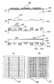
図1はこの発明による最も基本的な太陽電池作製プロセスのフローチャートの一例である。
すなわち、この発明においては、まず、準備された例えばp型シリコン基板に対し、濃度1〜数%の水酸化ナトリウム等のアルカリ水溶液でシリコンをエッチングすることにより表面にテクスチャーと呼ばれる凹凸構造を形成し、太陽電池表面で光の多重反射を生じさせることで、実効的に反射率を低減し変換効率を向上させる(ステップS1、S2)。なお、このテクスチャー構造のない場合についても、この発明は何ら問題なく適用できる。
FIG. 1 is an example of a flowchart of the most basic solar cell manufacturing process according to the present invention.
That is, in the present invention, first, a prepared concavo-convex structure called a texture is formed on the surface by etching silicon with an alkaline aqueous solution such as sodium hydroxide having a concentration of 1 to several percent on a prepared p-type silicon substrate, for example. By causing multiple reflection of light on the surface of the solar cell, the reflectance is effectively reduced and the conversion efficiency is improved (steps S1 and S2). Note that the present invention can be applied to any case without this texture structure without any problem.
次に、POCl3 によるリンの熱的な拡散によりn型拡散層を形成し(ステップS3)、そのn型拡散層の表面に反射防止膜を形成する(ステップS4)。その後、受光面銀ペースト電極の印刷・乾燥工程(ステップS5)、裏面アルミペースト電極の印刷・乾燥工程(ステップS6)、裏面ガラスペーストの印刷・乾燥工程(ステップS7)を経た後、焼成することにより太陽電池が完成される(ステップS8,S9)。なお、受光面側に反射防止膜を形成しない場合においても何らの問題なく、この発明を適用できる。また、ここで、表面電極と裏面電極の印刷の順番を入れ替えても問題はない。 Next, an n-type diffusion layer is formed by thermal diffusion of phosphorus with POCl3 (step S3), and an antireflection film is formed on the surface of the n-type diffusion layer (step S4). Then, after passing through the printing / drying step (step S5) of the light receiving surface silver paste electrode, the printing / drying step (step S6) of the back surface aluminum paste electrode, and the printing / drying step (step S7) of the back surface glass paste, firing is performed. Thus, the solar cell is completed (steps S8 and S9). Note that the present invention can be applied without any problem even when the antireflection film is not formed on the light receiving surface side. Here, there is no problem even if the printing order of the front electrode and the back electrode is changed.
このプロセスフローにより太陽電池が作製できることを図2を参照して説明する。
まず、図2(a)は、ガラスペーストによりシリコンが浸食され得ることを示すものである。
すなわち、p型単結晶シリコン基板表面にスクリーン印刷法を用いて幅400μmの線状のガラスペーストパターンを形成し、乾燥空気中100℃で10分問乾燥した後、同じく乾燥空気中650℃で数分間焼成した後のガラスペーストによるシリコンの浸食量を表面粗さ計で測定したものである。なお、浸食量の評価は、焼成後のガラスペーストを弗酸でエッチング除去した上で行っている。ガラスペーストのエッチング除去性はやや悪い為、外力の印加、例えば超音波などを加えると容易に除去できる。
It will be described with reference to FIG. 2 that a solar cell can be manufactured by this process flow.
First, FIG. 2 (a) shows that silicon can be eroded by glass paste.
That is, a linear glass paste pattern having a width of 400 μm is formed on the surface of a p-type single crystal silicon substrate by screen printing, dried for 10 minutes at 100 ° C. in dry air, and then several times at 650 ° C. in dry air. The amount of silicon erosion by the glass paste after baking for a minute was measured with a surface roughness meter. The evaluation of the amount of erosion is carried out after removing the fired glass paste with hydrofluoric acid. Etching removability of glass paste is somewhat poor and can be easily removed by applying external force, for example, applying ultrasonic waves.
この結果、図2(a)に示すように、シリコンはおよそ0.5μm程浸食されているのが分かる。以下に示すように、例えば原料としてPOCl3 を用いリンを熱的に拡散した拡散層の深さを0.3μmとしておけば、充分にこの拡散層を浸食・除去できる条件であると言える。この接合深さは、拡散温度や時間の調節で再現性良くコントロールできるものである。 As a result, as shown in FIG. 2A, it can be seen that silicon is eroded by about 0.5 μm. As shown below, for example, if the depth of the diffusion layer in which phosphorus is thermally diffused using POCl3 as a raw material is set to 0.3 μm, it can be said that the condition is sufficient for erosion and removal of this diffusion layer. This junction depth can be controlled with good reproducibility by adjusting the diffusion temperature and time.
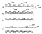
図2(b一1)及び(b一2)は、この方法により実際にpn接合の電気的分離が可能であるか否かを評価したサンプルの上面図及び断面図である。
図中、100は抵抗率が約2Ωcmのp型シリコン基板、101はPOCl3 により熱的にリンを拡散したn型拡散層であり、SIMS(Secondary Ion MassSpectroscopy)評価により約0.3μmの厚さであることを確認している。また、102は銀ペーストでなるn電極、103はアルミを数%含むアルミ銀ペーストでなるp電極、104はガラスペーストである。なお、ここでは、p電極103としてアルミ銀ペーストを用いたが、銀を含まないアルミペーストでも良く、以下に述べる効果は同様に得られることを確認している。
FIG. 2 (b 1) and FIG. 2 (b 1) are a top view and a cross-sectional view of a sample for evaluating whether or not pn junction can be electrically separated by this method.
In the figure, 100 is a p-type silicon substrate having a resistivity of about 2 Ωcm, 101 is an n-type diffusion layer in which phosphorus is thermally diffused by
また、図2(d)は図2(b一2)に示すサンプルを、700℃で数分間焼成した後の銀ペーストでなるn電極102とアルミ銀ペーストでなるp電極103の電極問の電流(縦軸)一電圧(横軸)特性(図中、with Glass Pasteと表記)及びガラスペーストパターンを形成せずに銀ペーストでなるn電極102とアルミ銀ペーストでなるp電極103のみをパターニングした場合の電流一電圧特性(図中、without Glass Pasteと表記)を示したものである。この結果から明らかなように、ガラスペースト104の存在により、明確なダイオード特性(整流性)が得られており、本方法がpn接合の電気的な分離に極めて有効であることが分かる。勿論のこと、焼成後のガラスペースト104は絶縁体であり、このガラスペースト104を除去したとしても図2(d)に示すダイオード特性が変ることはない。
FIG. 2D shows the current of the electrode between the
図番は前後するが、この結果から、図2(b一2)のサンプルを焼成した後のサンプルは、図2(c)に示すような形状になっていることは明らかである。この図2(c)に示すように、ガラスペースト104はn型拡散層101を浸食し、アルミ銀ペーストでなるp電極103下のn型拡散層101にはアルミが拡散し、該n型拡散層がp型に反転したp型反転層105が形成される。
Although the figure numbers are mixed, it is clear from this result that the sample after firing the sample of FIG. 2 (b-12) has a shape as shown in FIG. 2 (c). As shown in FIG. 2 (c), the
なお、本実施の形態では、n型拡散層101をPOCl3 により熱的にリンを拡散したものとしたが、他の方法、例えばリンあるいはヒ素のイオン注入やシラン系ガス、例えばモノシラン(SiH4)、ジシラン(Si2H6)、ジクロルシラン(SiCl2H2)、トリクロルシラン(SiCl3H)、テトラクロルシラン(SiCl4)と不純物原料としてのホスフィン(PH3)ガスを混合させたものを、熱あるいはプラズマ等の外的エネルギ一により分解して形成したn型拡散層を用いても同様な効果を得ることができる。
In the present embodiment, the n-
さらには、pn接合をへテロ接合として太陽電池の表面再結合抑制、窓効果などによる特性改善を図るため、例えばモノシランとメタンあるいはエタンなどの混合ガスより形成されるシリコンカーバイド(SiC)を用いてもよい。また、このような方法で形成される薄膜は、形成条件、例えば成膜温度などを変えることにより、非晶質、微結晶、多結晶あるいは単結晶とすることが可能である。また、その厚さも数百オングストロームから数μmであれば、ガラスペースト組成・焼成条件の工夫により同様な効果を得ることが可能である。 Furthermore, in order to improve the characteristics by suppressing the surface recombination of the solar cell, the window effect, etc. by using the pn junction as a heterojunction, for example, silicon carbide (SiC) formed from a mixed gas such as monosilane and methane or ethane is used. Also good. In addition, the thin film formed by such a method can be made amorphous, microcrystalline, polycrystalline, or single crystal by changing the forming conditions such as the film forming temperature. If the thickness is several hundred angstroms to several μm, the same effect can be obtained by devising the glass paste composition and firing conditions.
また、本実施の形態では、pn接合の電気的な分離を実現する手段の一例として、図2(b一2)に示すように、電極・ガラスペーストを全てパターニングした後、焼成を行う方法を示したが、ガラスペーストのパターニング・焼成後に電極形成を行う、あるいはガラスペーストのパターニング・焼成・エッチング除去後に電極形成を行う、また、電極のパターニング・焼成後、ガラスペーストをパターニング・焼成する、など様々な方法によっても前述したと同様なpn接合の電気的分離を図ることが可能である。また、具体的な焼成温度の条件としては、600〜950℃、数分から数十分の範囲で上述したpn接合の分離効果が得られることを確認している。 In this embodiment, as an example of means for realizing electrical isolation of the pn junction, as shown in FIG. 2 (b-12), a method of firing after patterning all of the electrode / glass paste is performed. As shown, electrode formation after patterning / firing of glass paste, electrode formation after patterning / firing / etching removal of glass paste, glass paste patterning / firing after patterning / firing of electrode, etc. It is possible to achieve electrical isolation of the pn junction as described above by various methods. Moreover, as specific firing temperature conditions, it has been confirmed that the above-described pn junction separation effect can be obtained within a range of 600 to 950 ° C. for several minutes to several tens of minutes.
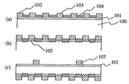
図3は上記の基本的な実験事実に基づき実際に太陽電池を作製した工程図を示すもので、図1に示すフローチャートに対応したものである。
図3における太陽電池の構造は、図17に示す従来例で説明したものと同様の場合である。ここでは、図3(a)に示すp型シリコン基板100として、厚さ600μm、サイズ10cm×10cm、比抵抗20Ωcm、面方位(100)の基板を用いた。図3(b)に示すn型拡散層101は上述したPOCl3 によるリンの熱的な拡散により形成した。拡散条件としては、例えば860℃、10分の処理により、拡散層シート抵抗として約50Ω/□、接合深さ0.3μmの拡散層を形成した。
FIG. 3 shows a process diagram for actually producing a solar cell based on the above basic experimental facts, and corresponds to the flowchart shown in FIG.
The structure of the solar cell in FIG. 3 is the same as that described in the conventional example shown in FIG. Here, as the p-
ここでは、図3(c)、(d)に示す位置にガラスペースト104を形成している点がポイントであり、ガラスペースト104のパターン幅は、例えば0.5〜2mmとした。なお、受光面(入射光面)に形成する銀ペーストでなるn電極107の形状は、図3(e)に示すような櫛型パターンとした(電極ピッチは、例えば2.5mm)。ここで、n電極107・ガラスペースト104の形成条件は、乾燥空気中にて700℃で7分問の焼成を行った。
Here, the point is that the
この方法で作製した太陽電池の特性は、図17(a)〜(e)による従来例の方法と遜色のないものが得られた。これは、図3(c)のエッジ部分115に示すように、BSF層4とn型拡散層101がガラスペースト104により電気的に分離されるためになされた結果である。また、図3には示していないが、図1のフローチャートに示すように、反射防止膜をn型拡散層2の表面に設けた後、受光面に形成される銀ペーストでなるn電極107、裏面に形成されるアルミペーストでなるp電極103、及びガラスペースト104を形成しても、全く同様の方法で太陽電池の作製が可能である。
The characteristics of the solar cell produced by this method were inferior to those of the conventional method shown in FIGS. 17 (a) to 17 (e). This is because the
この場合、焼成時にはn電極107の銀ペースト中に含まれるガラス成分が反射防止膜を突き破る現象(ファイヤースルー)によりn型拡散層101と電気的な接触が実現される為である。ここで、反射防止膜としては、例えばCVD法あるいはスパッタリング法等を用いて形成されるシリコン窒化膜(SiNx)、チタンオキサイド(TiOx)、シリコン酸化膜(SiOx)などであり、厚さは数百から1000オングストローム程度の厚さである。
In this case, the electrical contact with the n-
また、図3には示していないが、図1のフローチャートに示すように、一般に、テクスチャーと呼ばれる凹凸構造(後述の実施の形態6を参照)を基板表面に設けた後、上述のプロセス方法を適用してもこの発明に何らの妨げも無い。
さらに、反射防止膜の形成方法として、例えば減圧CVD法でシリコン窒化膜を形成するような場合、基板裏面側にもシリコン窒化膜が形成されてしまう。
しかし、この発明では、この例のように裏面に形成されてしまったシリコン窒化膜を除去することなく、前述した作製フローそのままで太陽電池が作製できることも確認した。これは、裏面に形成したガラスペースト104及びn電極107の銀ペースト中に含まれるガラス成分が裏面側のシリコン窒化膜をファイヤースルーすることにより、pn接合の電気的な分離、電極の半導体との接触が実現できるためである。勿論、シリコン窒化膜のみならず、他の反射防止膜材料に対しても同様である。
Although not shown in FIG. 3, as shown in the flowchart of FIG. 1, generally, after providing an uneven structure called texture (see Embodiment 6 described later) on the substrate surface, the above-described process method is performed. Even if applied, there is no hindrance to this invention.
Further, as a method for forming the antireflection film, for example, when a silicon nitride film is formed by a low pressure CVD method, a silicon nitride film is also formed on the back surface side of the substrate.
However, in the present invention, it was also confirmed that a solar cell can be manufactured with the above-described manufacturing flow as it is without removing the silicon nitride film formed on the back surface as in this example. This is because the
上述したように、この実施の形態によれば、従来例で述べたような基板裏面に形成された不要な拡散層のエッチング除去工程が全く不要になり、大幅に工程を簡略化することができる。
なお、ガラスペースト104と電極ペーストの形成のためのプロセスフローとしては、既に述べた様々な手順を選択できることは言うまでもない。また、この実施の形態において、基板の導電型が逆になった場合においても、後述する実施の形態4に示すものと同様な考え方で、この発明の適用が可能である。
さらに、この発明における電極及びガラスペーストパターンの形成には、上述したスクリーン印刷の他に、ロールコーター式の印刷方法を用いてもよい。
以上の様々なプロセス方法は以下で述べる幾つかの実施の形態の実現に当たっても、同様に適用できるものであり、太陽電池の構造やシリコンの結晶品質に依存して取捨選択が可能である。
As described above, according to this embodiment, the unnecessary step of removing the diffusion layer formed on the back surface of the substrate as described in the conventional example is completely unnecessary, and the process can be greatly simplified. .
It goes without saying that the various procedures described above can be selected as the process flow for forming the
Furthermore, in order to form the electrode and the glass paste pattern in the present invention, a roll coater type printing method may be used in addition to the screen printing described above.
The various process methods described above can be similarly applied to the realization of some embodiments described below, and can be selected depending on the structure of the solar cell and the crystal quality of silicon.
実施の形態2.
図4はこの発明による実施の形態2を説明するための太陽電池の製造プロセス及び構造について説明するものである。以下、図を用いて製造プロセスを順に説明する。
図4(a)は、実施の形態1と同様に、n型拡散層101を形成したp型シリコン基板100上に、ガラスペースト104のパターンを形成した状態を示している。そして、図4(b)は図4(a)に示すサンプルを焼成後、ガラスペースト104をエッチング除去した状態を示している。ここで、n型拡散層101は実施の形態1で示したメカニズムにより除去され、図4(b)に示すように、p型シリコン基板表面106が露出することになる。
FIG. 4 explains a solar cell manufacturing process and structure for explaining the second embodiment of the present invention. Hereinafter, the manufacturing process will be described in order with reference to the drawings.
FIG. 4A shows a state in which the pattern of the
図4(c)は、ガラスペースト104をパターニングしなかったn型拡散層101上に銀ペーストでなるn電極102とp型シリコン基板表面106上にアルミ銀ペーストでなるp電極103を形成した状態である。これらの電極パターンピッチは、1〜3mm程度である。
図4(d)は図4(a)〜(c)でプロセスを実施した面と対抗面(太陽電池として機能させる際に、主たる入射光面(受光面)となる)に形成されたn型拡散層101への電極を形成した状態を示している。ここで、107は主たる入射光面側に形成された銀ペーストでなるn電極であり、パターンピッチは2〜3mm程度である。
FIG. 4C shows a state in which an
FIG. 4D is an n-type formed on the surface opposite to the surface on which the process is performed in FIGS. 4A to 4C (which becomes the main incident light surface (light receiving surface) when functioning as a solar cell). The state which formed the electrode to the diffused
ここで、電極102、103、107の焼成は別々に実施しても良いが、プロセスの簡易化の為には、電極102、103、107を連続して印刷した後、同時に焼成を行ってもよい。なお、この主たる入射光面側に形成すべきn型拡散層101は、実施の形態1でも述べた様々な方法により形成可能であり、また、形成する順番も、裏面側のn型拡散層101と同時あるいは裏面側のn型拡散層101の形成後であっても良い。
Here, the
以上により完成される太陽電池の電極パターンの模式図を図4(e)及び(f)に示す。
この構造の太陽電池は、主たる入射光面側にn電極107、その裏面(対抗面)にn電極102及びp電極103を有する構造となっており、太陽電池の変換効率向上に有効な構造の一つとして知られているが(例えば、T.Warabisakoand K.Matsukuma, Technical Digest of the 7th lnternational Photovoltaic Science and Engineering Conference, Nagoya, Japan, 1993, pp.57)、このような構造の太陽電池も、この発明によれば簡単なプロセスで実現することが可能となる。
The schematic diagram of the electrode pattern of the solar cell completed by the above is shown to FIG.4 (e) and (f).
The solar cell having this structure has a structure having an n-
実施の形態3.
図5は前述した実施の形態2の太陽電池の構造を実現するための実施の形態3に係る製造方法を説明する工程図である。
上述した実施の形態2では、pn接合の電気的分離を行うのに、ガラスペースト104を除去する方法について説明したが、既に実施の形態1で述べたように必ずしもガラスペースト104を除去する必要はない。ここでは、ガラスペースト104を除去しない場合の太陽電池製造プロセスについての実施の形態についての説明を行う。
FIG. 5 is a process diagram illustrating a manufacturing method according to
In the above-described second embodiment, the method of removing the
図5(a)は、実施の形態1と同様に、n型拡散層101を形成したp型シリコン基板100上に、n電極102の銀ペーストパターンとp電極103のアルミ銀ペーストパターンを印刷し焼成した後の状態を示しており、105は既に説明したものと同等なp型反転層である。
また、図5(b)はn電極102とp電極103間の電気的な分離を行うためのガラスペースト104を印刷した状態、図5(c)はこれを焼成しpn接合を電気的に分離した後の状態、図5(d)は主たる入射光面側に銀ペーストでなるn電極107のパターンを形成した状態をそれぞれ示すものである。なお、ここに示すように、電極102、103及び107とガラスペースト104の焼成は別々に実施しても良いが、プロセスの簡易化の為には電極102、103及び107を印刷後、同時に焼成を行ってもよい。
以上のように、本実施の形態によれば、実施の形態2よりもさらに簡略化したプロセスで太陽電池を製造することが可能となる。
5A, in the same manner as in the first embodiment, the silver paste pattern of the
FIG. 5B shows a state in which a
As described above, according to the present embodiment, it is possible to manufacture a solar cell by a process further simplified than that of the second embodiment.
実施の形態4.
図6は実施の形態2の太陽電池構造を実現するための実施の形態4に係る製造方法を説明する工程図である。上述した実施の形態3では、図4(a)及び(b)に示すように、p電極、n電極、ガラスペーストパターンを分けて形成するようにしているが、さらに製造プロセスを簡略化するためには、以下の方法が有効である。
FIG. 6 is a process diagram for explaining the manufacturing method according to the fourth embodiment for realizing the solar cell structure of the second embodiment. In the above-described third embodiment, as shown in FIGS. 4A and 4B, the p electrode, the n electrode, and the glass paste pattern are separately formed. However, in order to further simplify the manufacturing process. The following methods are effective for this.
図6(a)は、n型拡散層101を形成したp型シリコン基板100上に、銀ペーストでなるn電極102のパターン、アルミ銀ペーストでなるp電極103のパターン、ガラスペースト104のパターンを全て印刷した後の状態を示し、図6(b)はこれを一度に焼成した状態を示している。なお、105は既に説明したものと同等なp型反転層である。
6A shows an
さらに、図6(c)は、主たる入射光面側に銀ペーストでなるn電極107のパターンを形成した状態を示すものである。なお、ここに示すように、電極102、103及び107とガラスペースト104の焼成は別々に実施しても良いが、プロセスの簡易化の為には電極102、103及び107とガラスペースト104を印刷後、全て同時に焼成を行ってもよい。
Further, FIG. 6C shows a state in which the pattern of the n-
以上のように、本実施の形態によれば、実施の形態3よりもさらに簡略化したプロセスで太陽電池を製造することが可能となる。
なお、実施の形態1〜4においては、特に最適条件を指定していないが、実際の太陽電池の製造方法の手順の選定、即ち電極材料、ガラスペーストの印刷順番、焼成温度及び焼成回数、焼成順番等の選定は、用いているシリコン結晶の品質に依存する所が大きいため、一義的には決まるものではなく、熱的な影響を考慮して決定されるべきものである。何れにせよ、この発明によれば、簡略化したプロセスで太陽電池を製造することが可能となることは明らかである。
As described above, according to the present embodiment, it is possible to manufacture a solar cell by a process further simplified than that of the third embodiment.
In
実施の形態5.
図7はこの発明によるさらに別の実施の形態5に係る太陽電池の製造方法について説明する工程図である。
上述した実施の形態1ないし4では、基板の導電型がp型の場合について説明を行ったが、この発明は基板がn型の場合でも適用可能である。
Embodiment 5 FIG.
FIG. 7 is a process diagram for explaining a method for manufacturing a solar cell according to still another embodiment 5 of the present invention.
In the first to fourth embodiments described above, the case where the conductivity type of the substrate is p-type has been described. However, the present invention can also be applied to the case where the substrate is n-type.
図7(a)で、108は例えば抵抗率が約2Ωcmのn型シリコン基板、109は例えばボロンを熱的に拡散したp型拡散層である。なお、このp型拡散層109としては、ボロンなどの不純物のイオン注入あるいはシラン系ガスとジボラン(B2H6)ガスを混合させたものを、熱あるいはプラズマ等の外的エネルギーにより分解して形成したp型シリコン層を用いてもよく、その厚さも数百オングストロームから数μmであれば、実施の形態1で説明したと同じ理由により、以下に説明する効果を奏することが可能である。
In FIG. 7A, 108 is an n-type silicon substrate having a resistivity of about 2 Ωcm, for example, and 109 is a p-type diffusion layer in which boron is thermally diffused, for example. The p-
本実施の形態では、まず、このp型シリコン層109上に、ガラスペースト104をスクリーン印刷によりパターニングする。パターン形状・ピッチ等は既に実施の形態2等で述べたものと同様で良い。図7(b)は、図7(a)を焼成した後、ガラスペースト104を弗酸でエッチング除去した後の状態を示している。ガラスペースト104の性質上、対象となるシリコンの導電型がn、pを問わず焼成により浸食し、その結果、図7(b)に示すような形状を得ることができる。ここで、110はガラスペースト104により浸食され露出したn型シリコン基板表面である。
In the present embodiment, first,
このn型シリコン基板表面110上にn型電極102となる銀ペーストパターン、部分的に残されたp型拡散層109上にp電極103となるアルミ銀ペーストパターンを印刷・焼成した後の状態が図7(c)である。さらに、図7(a)〜(c)でプロセスを実施した面と対抗面(太陽電池として機能させる際に、主たる入射光面(受光面)となる)に形成されたp型拡散層109上にp電極111となるアルミ銀ペースト電極を形成した状態を図7(d)に示す。
The state after printing and baking the silver paste pattern to be the n-
ここで、電極102、103と111の焼成は別々に実施しても良いが、プロセスの簡易化の為には、電極102、103と111の印刷後、同時に焼成を行ってもよい。なお、この主たる入射光面側に形成すべきp型拡散層109は、上述した様々な方法により形成可能であり、また、形成する順番も、裏面側のp型層と同時あるいは裏面側のp型層形成後であっても良い。
以上により完成される太陽電池の電極パターンの模式図を図7(e)及び(f)に示す。また、p電極111としてアルミ銀ペーストの代わりに銀を含まないアルミペーストを用いることも可能である。
Here, the
The schematic diagram of the electrode pattern of the solar cell completed by the above is shown to FIG.7 (e) and (f). Moreover, it is also possible to use the aluminum paste which does not contain silver for the
実施の形態6.
図8はこの発明による実施の形態6を説明するための太陽電池の構造を示すもので、同図(a)はその断面構造図、同図(b)は外観図を示したものである。 ここに示した構造は、実施の形態2〜5で示したものとは異なり、基板にバイアホール113を設けたp型シリコン基板112を用いていることが特徴であり、このバイアホール113側面にもn型拡散層101を設けることにより、発生した電流を太陽電池裏面に配置したn電極102及びp電極103で集電するものである。
このような構造にする理由は、発電に寄与するp型シリコン基板112を薄くした場合、発生電流の低下は避けられないため、電極を全て裏面に配置することにより、受光面積を増し、光電流の増加を図ることを目的としているからである。
Embodiment 6 FIG.
FIG. 8 shows the structure of a solar cell for explaining Embodiment 6 according to the present invention. FIG. 8 (a) is a sectional structural view thereof, and FIG. 8 (b) is an external view thereof. Unlike the structures shown in the second to fifth embodiments, the structure shown here is characterized by using a p-
The reason for adopting such a structure is that when the p-
本構造を実現するための基本プロセスは、例えばM.Deguchi等によって示されているが(Conference Record of IEEE First World Conference on Photovoltaic Energy Conversion, Hawaii, voI.II, pp.1287(1994))、ここでは、そのプロセス方法の詳細な説明は省略する。
この発明を、このような太陽電池構造に適用した場合の最終構造のみを、図8(a)、(b)及び(c)に示す。
The basic process for realizing this structure is shown by, for example, M. Deguchi (Conference Record of IEEE First World Conference on Photovoltaic Energy Conversion, Hawaii, voI.II, pp.1287 (1994)). Then, detailed explanation of the process method is omitted.
Only the final structure when this invention is applied to such a solar cell structure is shown in FIGS. 8 (a), (b) and (c).
図8(a)はp型シリコン基板112の全面にn型拡散層101を設けた後、実施の形態2、3あるいは実施の形態4に示すのと同様なプロセスで、電極形成とpn接合の電気的な分離をなし得た状態である。なお、ここに、n型拡散層101は、実施の形態1で述べたような様々な方法で形成することができる。
図8(c)は電極配置面の上面図であるが、ここに示すようなパターンでpn接合の分離及び電極パターンの配置を実現することにより、バイアホール113を有するp型シリコン基板112を用いた太陽電池に対しても、この発明は適用可能である。
In FIG. 8A, after the n-
FIG. 8C is a top view of the electrode arrangement surface. By realizing the separation of the pn junction and the arrangement of the electrode pattern with the pattern shown here, the p-
なお、図8中、114は一般にテクスチャーと呼ばれる表面の凹凸構造で、面方位が(100)のシリコン基板を用いる場合には、濃度1〜数%の水酸化ナトリウム等のアルカリ水溶液でシリコンをエッチングすることにより形成可能であるが、これを設けることにより、太陽電池表面で光の多重反射が生じ、実効的に反射率を低減し変換効率を向上できる。 In FIG. 8, 114 is an uneven structure of the surface generally called texture. When a silicon substrate having a (100) plane orientation is used, silicon is etched with an alkaline aqueous solution such as sodium hydroxide having a concentration of 1 to several percent. However, by providing this, multiple reflection of light occurs on the surface of the solar cell, effectively reducing the reflectance and improving the conversion efficiency.
実施の形態1〜5では説明を簡単にするために、このテクスチャー構造のない場合について説明したが、勿論、このテクスチャー構造を有していても、この発明は何ら問題なく適用できる。
またさらに、説明の簡略化の為に、受光面側に反射防止膜を形成しない状態の構造について実施の形態2〜6で説明したが、実施の形態1で述べたような方法により反射防止膜を設けた場合においても何らの問題なく、この発明を適用できることは言うまでもない。
In the first to fifth embodiments, the case where this texture structure is not provided has been described in order to simplify the description. Of course, the present invention can be applied without any problem even if this texture structure is provided.
Furthermore, for the sake of simplification, the structure in which the antireflection film is not formed on the light receiving surface side has been described in the second to sixth embodiments. However, the antireflection film is formed by the method described in the first embodiment. Needless to say, the present invention can be applied without any problem even in the case of providing the above.
実施の形態7.
上述した実施の形態1ないし6は、太陽電池の電極形成においてpn接合の電気的な分離を容易に実現する製造方法について述べたものであるが、この実施の形態7では、太陽電池の電極形成の際のpn接合の電気的な分離方法と同様な物理現象を適用して半導体基板との接触抵抗を大幅に低減し得る電極を形成することができる半導体装置の製造方法について詳述する。
すなわち、後述する実施の形態7以下における半導体装置の製造方法では、主としてシリコン半導体装置に関し、特に、窒化シリコン膜あるいは酸化チタン膜をシリコン基板表面に有する構造体において、金属ペースト材料を用いた場合の電極形成方法を簡略化し生産性を高めると共に、金属ペースト材料でなる電極とシリコン間の接触抵抗の低抵抗化を図り得る新規な半導体装置の製造方法を提供する。
That is, the method for manufacturing a semiconductor device according to the seventh embodiment or later to be described later mainly relates to a silicon semiconductor device, particularly when a metal paste material is used in a structure having a silicon nitride film or a titanium oxide film on the surface of a silicon substrate. Provided is a novel semiconductor device manufacturing method capable of simplifying an electrode forming method and improving productivity and reducing a contact resistance between an electrode made of a metal paste material and silicon.
このような半導体装置の製造方法が適用可能な半導体装置の種類は多岐に亘るが、中でも、フォトダイオードや太陽電池等の受光素子にとりわけ有効である。ここでは、具体例として太陽電池を取り上げ、発明の背景について説明する。
現在、地球上で用いられる電力用太陽電池の主流はシリコン太陽電池であるが、その量産レベルにおけるプロセスフローは、なるべく簡素化して製造コストの低減を図ろうとするのが一般的であり、中でも電極形成に関しては、金属ペーストをスクリーン印刷等で形成する方法が採られている。
There are a wide variety of types of semiconductor devices to which such a method for manufacturing a semiconductor device can be applied. Among them, the method is particularly effective for light receiving elements such as photodiodes and solar cells. Here, taking a solar cell as a specific example, the background of the invention will be described.
Currently, silicon solar cells are the mainstream of power solar cells used on the earth, but the process flow at the mass production level is generally as simple as possible to reduce the manufacturing cost. Regarding the formation, a method of forming a metal paste by screen printing or the like is employed.
一般的に行われている太陽電池作製フローで、反射防止膜を形成する前迄の工程は、図17(a)〜(d)に示す作製フローに従い、その後、n型拡散層2の表面に反射防止膜が形成される。
図9と図10は上記反射防止膜形成後の表面電極形成方法の例を示すフローチャートである。
図9は例えば特公平5−72114号公報に開示された方法を、また、図10は例えば特公平3−46985号公報に開示されている方法を示している。
In the solar cell manufacturing flow that is generally performed, the steps up to the formation of the antireflection film follow the manufacturing flow shown in FIGS. 17 (a) to 17 (d), and then on the surface of the n-
FIG. 9 and FIG. 10 are flowcharts showing an example of the surface electrode forming method after forming the antireflection film.
FIG. 9 shows a method disclosed in, for example, Japanese Patent Publication No. 5-72114, and FIG. 10 shows a method disclosed in, for example, Japanese Patent Publication No. 3-46985.
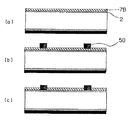
図9の場合は、図17(a)〜(d)に示すプロセスの後、反射防止膜7AがプラズマCVD法により形成された窒化シリコン膜からなる場合の電極形成方法である。この場合には、まず、窒化シリコン膜でなる反射防止膜7Aを表面電極が形成される部分のみ選択的にエッチング除去する(図9(a)→(b))。これにより、絶縁物である窒化シリコン膜を除去した部分はn型拡散層2が露出しており、ここに、直接、銀ペースト電極5Aを印刷し、乾燥・焼成工程を経て、表面電極形成が完了する(図9(c))。
The case of FIG. 9 is an electrode formation method when the
図10の場合は、図17(a)〜(d)に示す示すプロセスの後、反射防止膜7BがCVD法等によって形成された酸化チタン膜からなる場合の電極形成方法である。この場合には、図9とは異なり、酸化チタン膜上に直接、表面電極となる銀ペースト電極5Bを印刷し、乾燥・焼成工程を行う(図10(a)→(b))。これにより、酸化チタン膜でなる反射防止膜7Bは溶融し、銀ペースト電極5Bはn型拡散層2に到達し接触するので、電気的な接触が図られる(図10(c))。
The case of FIG. 10 is an electrode formation method in the case where the antireflection film 7B is made of a titanium oxide film formed by a CVD method or the like after the processes shown in FIGS. In this case, unlike FIG. 9, the silver paste electrode 5B which becomes a surface electrode is printed directly on the titanium oxide film, and a drying and baking process is performed (FIG. 10 (a)-> (b)). As a result, the antireflection film 7B made of a titanium oxide film is melted and the silver paste electrode 5B reaches and contacts the n-
この様な方法は、一般に、ファイヤースルーと言われるものであり、古くから知られている現象である。特に、この従来例にあるように、酸化チタン膜やシリコン酸化膜では、比較的容易にファイヤースルーが生じることも知られている。しかし、図17(a)〜(d)に示すようなpn接合型の太陽電池で、n型の浅い拡散層2に対して銀ペースト電極5を形成する際には、例えば高温で焼成しすぎると、pn接合破壊が生じるなどの問題がある。この点に関して、銀ペーストに周期表第5族の元素を混入し、焼成時に第5族の元素をn型拡散層2に拡散させることで、n型拡散層2の破壊を抑制する方法も提案されている。
Such a method is generally called fire-through and is a phenomenon that has been known for a long time. In particular, as in this conventional example, it is known that fire-through occurs relatively easily in a titanium oxide film or a silicon oxide film. However, when the silver paste electrode 5 is formed on the n-type
このような例は、例えば特公平4−67347号公報に、リン、ヒ素、アンチモンなどを混合することが開示されている。また、図10で示した特公平3−46985号公報による例では、周期表第5族の元素、具体例としてリンが酸化チタン膜やシリコン酸化膜からなる反射防止膜と反応し、ファイヤースルーを促進し易くなることが示されている。 Such an example is disclosed, for example, in Japanese Patent Publication No. 4-67347 in which phosphorus, arsenic, antimony, or the like is mixed. Further, in the example of Japanese Patent Publication No. 3-46985 shown in FIG. 10, an element of Group 5 of the periodic table, specifically, phosphorus reacts with an antireflection film made of a titanium oxide film or a silicon oxide film, It has been shown to be easier to promote.
以上のように、シリコン太陽電池の電極形成方法に関しては様々な工夫がなされているが、特に、窒化シリコン膜を反射防止膜とした太陽電池では、ファイヤースルーを行うに至っておらず、図9に示すようなプロセスを必要としていた。あるいは、図10に示すように銀ペースト電極にリンに代表されるような周期表第5族の元素を混入し、ファイヤースルーを促進する方法も提案されているが、窒化シリコン膜に対してのファイヤースルーによる電極形成の可能性については開示されていない。 As described above, various contrivances have been made for the electrode formation method of the silicon solar cell. In particular, in the solar cell using the silicon nitride film as the antireflection film, the fire-through has not been performed. I needed a process as shown. Alternatively, as shown in FIG. 10, a method of promoting the fire-through by mixing elements of Group 5 of the periodic table such as phosphorus into the silver paste electrode has been proposed. The possibility of forming electrodes by fire-through is not disclosed.
そこで、この実施の形態7では、従来困難であった窒化シリコン膜を用いた場合でもファイヤースルーを可能として、半導体基板との接触抵抗を大幅に低減し得る半導体装置の製造方法を提供する。また、酸化チタン膜のファイヤースルーを利用して電極形成を行う半導体装置においても、従来方法よりも太陽電池の性能が改善され、また、接触抵抗も大幅に低減し得る半導体装置の製造方法を提供する。 In view of this, the seventh embodiment provides a method for manufacturing a semiconductor device that enables fire-through even when a silicon nitride film, which has been difficult in the past, is used, and that can greatly reduce the contact resistance with the semiconductor substrate. Also, a semiconductor device manufacturing method in which the performance of a solar cell is improved as compared with the conventional method and the contact resistance can be greatly reduced in a semiconductor device in which electrodes are formed using a fire-through of a titanium oxide film. To do.
この実施の形態7において、金属ペースト材料は半導体基板上に形成した絶縁膜を溶融・貫通する性質を有するものであるが、これを実現する為には、金属ペースト材料中に混合するフリット状のガラスの成分がポイントとなる。本発明者の実験によれば、例えばガラスの主成分として、鉛(Pb)5−30%、ボロン(B)5−10%、シリコン(Si)5−15%、酸素(O)30−60%の組成を基本とすることで、後述する以下の実施の形態で示す効果を平易に奏することができることが明らかにされた。なお、本実施の形態ではこれらの組成のガラスに加え、ジエチレングリコール・モノブチルエーテル(Diethyleneglycol Monobtylether)及びエチレングリコール・モノメチルエーテル(Ethyleneglycol Monobtylether)等を適量混合し、スクリーン印刷可能な所定の粘度に調整して用いた。また、従来の技術で紹介したような周期表第5族の元素を混入させた金属ペースト材料を用いる必要性がないことも併せて確認した。以下の半導体装置に係る具体的な実施の形態で使用する金属ペースト材料は特に断わりがない限り、このような金属ペースト材料を用いている。 In the seventh embodiment, the metal paste material has a property of melting and penetrating an insulating film formed on the semiconductor substrate. In order to realize this, a frit-like material mixed in the metal paste material is used. The glass component is the point. According to the experiments by the present inventors, for example, as a main component of glass, lead (Pb) 5-30%, boron (B) 5-10%, silicon (Si) 5-15%, oxygen (O) 30-60. It has been clarified that the effects shown in the following embodiments described later can be easily achieved by using the composition of% as a basis. In the present embodiment, in addition to the glass having these compositions, diethylene glycol monobutyl ether (Diethyleneglycol Monobtylether), ethylene glycol monomethyl ether (Ethyleneglycol Monobtylether) and the like are mixed in an appropriate amount, and adjusted to a predetermined viscosity capable of screen printing. Using. It was also confirmed that there was no need to use a metal paste material mixed with elements of Group 5 of the periodic table as introduced in the prior art. As long as there is no notice in particular, the metal paste material used by the following specific embodiment concerning a semiconductor device uses such a metal paste material.
図11はこの実施の形態7及び後述する実施の形態9に係る半導体装置の製造方法に関するフローチャートである。
以下、このフローチャートに基づいて具体的な実施の形態について説明する。なお、本プロセスフローは1つの半導体装置に限定されるものではないが、以下、具体例として太陽電池を取り上げて説明する。
FIG. 11 is a flowchart relating to the semiconductor device manufacturing method according to the seventh embodiment and a ninth embodiment to be described later.
A specific embodiment will be described below based on this flowchart. The process flow is not limited to one semiconductor device, but a solar cell will be described below as a specific example.
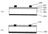
この実施の形態7では、図11に示すフローチャートで、ステップS11−ステップS12−(ステップS13)−ステップS14−ステップS15a−(ステップS16)−ステップS17−(ステップS18)−ステップS19−ステップS20のフローで作製される太陽電池について、図12に示す特徴的な断面構造を参照して説明を行う。なお、図11において、括弧付の工程、例えば(ステップS3)等は、太陽電池の製造工程で本質的に必要とされるものではなく、本工程の付加によりさらに特性改善が図れるものあるいは工程を簡略化する上で省略しても良いものであることを示している。 In the seventh embodiment, in the flowchart shown in FIG. 11, step S11-step S12- (step S13) -step S14-step S15a- (step S16) -step S17- (step S18) -step S19-step S20. The solar cell manufactured by the flow will be described with reference to a characteristic cross-sectional structure shown in FIG. In FIG. 11, the steps in parentheses, such as (Step S3), are not essentially required in the manufacturing process of the solar cell, and the steps or steps that can further improve the characteristics by adding this step. It is shown that it may be omitted for simplification.
まず、図11のステップS11は、半導体基板として例えば引き上げ法により製造される単結晶あるいは鋳造法により製造される多結晶シリコン基板を洗浄する工程であるが、太陽電池の場合、インゴットからスライスされたままの基板を用いることが多い。この場合、スライスに用いたワイヤーソー等の傷による基板表面ダメージおよびウエハスライス工程の汚染を取り除くため、水酸化カリウム、水酸化ナトリウム水溶液等のアルカリ水溶液あるいは弗酸と硝酸の混合液などを用いて、およそ10から20μm程度、基板表面をエッチングする。さらには、基板表面に付着した鉄などの重金属類の除去のために、塩酸と過酸化水素の混含液で洗浄する工程を付加しても良い。図12(a)では、この工程により得られたシリコン基板を符号200で示した。
First, step S11 in FIG. 11 is a step of cleaning a single crystal manufactured by, for example, a pulling method or a polycrystalline silicon substrate manufactured by a casting method as a semiconductor substrate, but in the case of a solar cell, it is sliced from an ingot. In many cases, the substrate is used as it is. In this case, in order to remove substrate surface damage and contamination of the wafer slicing process due to the wire saw used for slicing, an alkaline aqueous solution such as potassium hydroxide or sodium hydroxide aqueous solution or a mixed solution of hydrofluoric acid and nitric acid is used. The substrate surface is etched by about 10 to 20 μm. Further, a step of washing with a mixed solution of hydrochloric acid and hydrogen peroxide may be added to remove heavy metals such as iron adhering to the substrate surface. In FIG. 12A, the silicon substrate obtained by this process is denoted by
引き続き、ステップS12で、使用する基板が例えばp型シリコン基板200であれば、pn接合を形成する為にn型拡散層201を形成する。このn型拡散層の形成方法は、図17(b)で説明したようなオキシ塩化リン(POCl3)によるリン拡散を用いる。その他の方法としては、例えばリンあるいはヒ素のイオン注入やシラン系ガス、例えばモノシラン(SiH4)、ジシラン(Si2H6)、ジクロルシラン(SiCl2H2)、トリクロルシラン(SiCl3H)、テトラクロルシラン(SiCl4)と不純物原料としてのホスフィン(PH3)ガスを混合させたものを、熱あるいはプラズマ等の外的エネルギーにより分解して形成したn型シリコン層を用いても同様の効果を得ることができる。さらには、pn接合をヘテロ接合として太陽電池の表面再結合抑制、窓効果などによる特性改善を図るため、例えばモノシランとメタンあるいはエタンなのど混合ガスより形成されるシリコンカーバイド(SiC)を用いてもよい。
Subsequently, in step S12, if the substrate to be used is a p-
すなわち、シリコン基板に形成される接合が、周期表第3族あるいは第5族に属する元素を不純物として用いた第4族からなる半導体層を用いて構成するようにすることで、簡便な方法でpn接合を形成することができ、また、第4族の元素からなる半導体層が、直接シリコン基板への不純物拡散もしくはイオン注入により形成された半導体層あるいはシリコン基板表面に原料ガスの熱もしくはプラズマによる分解反応により堆積・形成される単元素もしくは複数の元素からなる半導体薄膜層を用いることにより、この半導体層の不純物濃度、厚さ等を高い精度で制御できる。また、このような方法で形成される薄膜は、形成条件、例えば成膜温度などを変えることにより、非晶質、微結晶、多結晶あるいは単結晶とすることが可能であり、不純物のドーピング量もコントロールできる。また、その厚さも数百オングストロームから数μmの範囲で、目的に合わせて任意に選択すれば良い。以上のように形成されるn型拡散層を、図12(a)中で符号201で示した。
That is, the junction formed on the silicon substrate is configured by using a semiconductor layer made of
次に、ステップS13の基板表裏面のpn接合分離は、図17(c)に示すようなフローで行うことが可能である。また、上記ステップS12で述べたような、イオン注入やCVD法によるn型層形成プロセスを選択する場合には、基本的に片面にのみn型層が形成されているので、図17(c)に示すようなフローは必ずしも必要としない。またさらには、リンが含まれる液体塗布材料、例えばPSG(Phospho‐Slicate‐Glass)などを基板の1面のみにスピンコートして、適当な条件でアニールする拡散方法を用いるような場合にも、図17(c)に示すようなフローは必ずしも必要としない。勿論、基板裏面までn型層が形成されている恐れのある場合には、本工程を採用することで、完全性を高めることができる。 Next, the pn junction separation of the front and back surfaces of the substrate in step S13 can be performed by a flow as shown in FIG. When the n-type layer formation process by ion implantation or CVD method as described in step S12 is selected, since the n-type layer is basically formed only on one side, FIG. The flow shown in Fig. 1 is not necessarily required. Furthermore, even when using a diffusion method in which a liquid coating material containing phosphorus, such as PSG (Phospho-Slicate-Glass), is spin-coated on only one surface of the substrate and annealed under appropriate conditions, The flow as shown in FIG. 17C is not necessarily required. Of course, when there is a possibility that the n-type layer is formed up to the back surface of the substrate, the use of this process can improve the integrity.
ステップS14は、上記のようにしてn型拡散層201を形成した基板を、例えば熱酸化法により熱酸化(酸素中、800℃から1000℃で数分間処理)することで、基板表面(特にn型拡散層表面)に適当な厚み、例えば100から200オングストローム程度のシリコン酸化膜を形成する工程である。この工程により、n型拡散層表面のみならず、対向面のp型シリコン基板200表面にも酸化膜が形成されるが、この酸化膜の形成により、n型拡散層表面および対向面のp型シリコン基板表面の欠陥密度(表面準位密度)が低減し表面再結含が抑制されることにより、太陽電池特性が改善される。この方法は、表面パッシベーション技術の一つとして広く知られているものである。また、シリコン酸化膜は、SiH4と02 の混合ガスを原料としたプラズマCVD法または熱CVD法により形成しても良い。図12(a)では、上記の方法で得られるシリコン酸化膜202が特にn型拡散層201の表面に形成された場合の構造を示した。
In step S14, the substrate on which the n-
ステップS15aは、窒化シリコン膜203(図12(a)参照)を形成する工程である。前記のステップS14を実施した場合、シリコン酸化膜202上に形成される構造となるが、先述したように、太陽電池の構成上、シリコン酸化膜202は本質的には必要ではないので、直接n型拡散層201上に形成しても良い。この窒化シリコン膜203は反射防止膜として機能するため、太陽電池の入射光に対する表面反射率を低減させることができ、このため、大幅に発生電流を増加させることが可能になる。窒化シリコン膜203の厚さは、その屈折率にもよるが、例えば1.9から2.0程度の屈折率の場合に700から800オングストローム程度が適当である。
Step S15a is a step of forming the silicon nitride film 203 (see FIG. 12A). When step S14 is performed, the structure is formed on the
この窒化シリコン膜203の形成方法は、減圧熱CVD法やプラズマCVD法を用いて形成される。熱CVD法の場合、ジクロルシラン(SiCl2H2)とアンモニア(NH3)を原料とすることが多く、例えばガス流量比としてNH3/SiCl2H2=10から20、反応室内の圧力0.2から0.5Torr、温度760℃の条件で成膜を行う。この方法では、高温熱分解の為、窒化シリコン膜203中には殆ど水素は含まれず、SiとNの組成比は、ほぼ化学量論的組成であるSi3N4となり、屈折率もほぼ1.96から1.98の範囲になる。従って、このような膜の場合、後工程で熱処理が加えられても膜質(膜厚、屈折率)が変化しない極めて緻密な膜質であるという特徴を有する。
The
また、プラズマCVD法で形成する場合の原料ガスとしては、SiH4とNH3の混合ガスを用いるのが一般的である。成膜条件としては、例えばガス流量比NH3/SiH4=0.5から1.5、反応室内の圧力1から2Torr、温度300から550℃で、プラズマ放電に必要な高周波電源の周波数としては数百kHz以上が適当である。このプラズマCVD法の場合、熱CVD法に比べて低温成膜のため、窒化シリコン膜203中には水素が含まれること、また、ガス分解がプラズマによるためSiとNの組成比も大きく変化させることができる等の特徴を有する。具体的に、ガス流量比、圧力、温度等の条件を変化させることで、Si、N、水素の組成比が変化し、屈折率で、およそ1.8から2.5の範囲の屈折率の窒化シリコン膜を形成できる。このような膜質の場合、後工程で熱処理が加えられた場合、例えば電極焼成工程等で、水素が離脱するなどの現象により、屈折率、膜厚が成膜直後の値から変化する場合がある。この場合には、あらかじめ後工程での熱処理による膜質変化を考慮して、成膜条件を決定するように対応すれば、太陽電池として必要な窒化シリコン膜を得ることが可能になる。
In addition, a mixed gas of SiH4 and NH3 is generally used as a source gas in the case of forming by plasma CVD. As the film forming conditions, for example, the gas flow ratio NH3 / SiH4 = 0.5 to 1.5, the pressure in the reaction chamber is 1 to 2 Torr, the temperature is 300 to 550 ° C., and the frequency of the high frequency power source necessary for plasma discharge is several hundreds. kHz or more is appropriate. In the case of this plasma CVD method, the
ステップS16についての詳細は後述するので、次工程以降の説明を先に行う。ステップS17はウエハ裏面に電極材料をスクリーン印刷法で所定のパターンのこの発明による金属ペースト材料として銀アルミもしくはアルミペーストでなる電極204(図12(a)参照)を印刷し乾燥する工程であり、ステップS18は、このペーストを焼成する工程である。具体的には、乾燥空気中で、例えば700から800℃の温度で数十秒から数分間焼成することで、p型基板とのオーミック接触を得るものであり、アルミがシリコン基板中に拡散した拡散層205(図12(b)参照)が形成される。 Since details of step S16 will be described later, the subsequent steps will be described first. Step S17 is a step of printing and drying an electrode 204 (see FIG. 12A) made of silver aluminum or aluminum paste as a metal paste material according to the present invention having a predetermined pattern by screen printing on the back surface of the wafer, Step S18 is a step of firing this paste. Specifically, by baking in dry air, for example, at a temperature of 700 to 800 ° C. for several tens of seconds to several minutes, ohmic contact with the p-type substrate is obtained, and aluminum diffuses into the silicon substrate. A diffusion layer 205 (see FIG. 12B) is formed.
ステップS19は、この発明による銀ペースト電極206をn型拡散層201側に形成した窒化シリコン膜203上に直接印刷し乾燥するものである。この後のステップS20では、銀ペースト206の焼成を行う工程であるが、前記のこの発明によるガラス成分を含む銀ペースト、銀アルミもしくはアルミペーストを用いる限り、ステップS18は不要であり、ステップS17およびS19で印刷・乾燥した各電極材料は一括してステップS20により焼成を行うことができる。この発明ではこのステップS20迄で、従来なし得なかった、窒化シリコン膜203に対するファイヤースルーが容易に実現され、図12(b)に示すように、ファイヤースルー後の銀ペースト電極206は、窒化シリコン膜203とシリコン酸化膜202を溶融・貫通しn型拡散層201と電気的な接触を取ることが可能になる。
In step S19, the
この点に関し、以下、実験事実に基づき詳細な説明を行う。
先述したように、通常、プラズマCVD法による窒化シリコン膜よりも熱CVD法による窒化シリコン膜は緻密であり、一層ファイヤースルーを実現するのは困難であることが容易に予測されるが、この発明によれば、成膜方法によらず容易に受光面電極側のオーミック接触を得ることができる。
図13は、図12に示す構造で実際に太陽電池を作製し、その特性、特にファイヤースルーで充分な低抵抗のオーミック接触が得られているかの目安になる、フィルファクター(FF)との関係を実験的に調べた結果である。
This point will be described in detail below based on experimental facts.
As described above, the silicon nitride film formed by the thermal CVD method is usually denser than the silicon nitride film formed by the plasma CVD method, and it is easily predicted that it is difficult to realize further fire-through. Therefore, ohmic contact on the light-receiving surface electrode side can be easily obtained regardless of the film forming method.
FIG. 13 shows the relationship with the fill factor (FF), which is a measure of whether or not a solar cell is actually manufactured with the structure shown in FIG. It is the result of having investigated experimentally.
この実験は、半導体基板としては、鋳造法による多結晶シリコン、n型拡散層201はオキシ塩化リン(POCl3)によるリン拡散法、シリコン酸化膜202は熱酸化法を用い、窒化シリコン膜203の成膜方法に関しては、プラズマCVD法、減圧熱CVD法の両方を検討したものである。電極の焼成は、図12(a)中の電極204と206を同時に焼成しており、乾燥空気中で実施した。また、焼成時間は焼成温度(ピーク値)675、700℃では45秒、720℃〜750℃では22秒、775℃〜800℃では10秒とした。なお、太陽電池サイズは全て10cm×10cmである。図13中に示すように、ほぼ全ての焼成条件で、10cm×10cmの実用的サイズの太陽電池において、0.76以上のフィルファクターが得られており、この発明の有効性を確認することができた。
In this experiment, polycrystalline silicon by casting is used as a semiconductor substrate, phosphorus diffusion by phosphorus oxychloride (POCl 3) is used for the n-
図12中に示すプラズマCVD法による窒化シリコン膜203の屈折率は、2.1で膜厚750オングストロームの場合であるが、他の屈折率として1.9、2.0、2.2、2.3、2.4の膜に対しても同様の結果が得られることを確認した。なお、上記の説明中、ステップS16に関する説明を省略したが、この工程は以下の状況を想定したものである。例えば減圧CVD法で窒化シリコン膜203を形成する場合、基板はその周辺の一部のみを固定する方法が取られることが多く、この場合、窒化シリコン膜203は、図12のように片面のみならず、その対向面にも形成されてしまう。その場合、対向面に形成された窒化シリコン膜は、裏面の電極204を形成する際の妨げになる場合がある。すなわち、ファイヤースルーできない場合には、基板200との電気的な接触の妨げとなってしまうのである。
The refractive index of the
従って、このような状況を回避するため、例えば部分的に対向面に形成された窒化シリコン膜の一部あるいは全体を除去した上で電極形成を行うことで、基板200との電気的接触を可能にするものがステップS16での工程である。しかし、この発明による銀アルミあるいはアルミペーストを用いる場合には、前記の焼成条件で窒化シリコン膜203をファイヤースルーできることが確認されており、必ずしも本工程を必要とするものではない。なお、プラズマCVD法で形成される窒化シリコン膜が裏面側に存在しても、全く同様にファイヤースルーできることも併せて確認している。即ち、この発明では、むしろ、積極的にあるいは不可抗力で基板の両面に窒化シリコン膜が形成された場合でも、一切のパターニング工程を必要とせずに太陽電池が製造できることになる。
Therefore, in order to avoid such a situation, it is possible to make electrical contact with the
実施の形態8.
この実施の形態8では、図11に示す工程のうち、実施の形態7以降のステップS21及びS22による発明についての説明を行う。特に、ステップS22がこの発明に係る特徴的な工程であり、ステップS20を経た太陽電池を、弗酸(HF)水溶液中に浸漬するものである。なお、浸漬後は純水で充分に洗浄したのち乾燥する。
Embodiment 8 FIG.
In the eighth embodiment, of the steps shown in FIG. 11, the invention according to steps S21 and S22 after the seventh embodiment will be described. In particular, step S22 is a characteristic process according to the present invention, in which the solar cell that has undergone step S20 is immersed in an aqueous hydrofluoric acid (HF) solution. After the immersion, the substrate is thoroughly washed with pure water and then dried.
図14に実際の実験結果を示す。なお、ここで示したものは、窒化シリコン膜203を減圧熱CVD法で形成した場合の太陽電池についての結果である。焼成条件は、実施の形態7よりも焼成条件を長目に実施した場合、例えば720℃で5分間の焼成を行った場合のものである。焼成直後のフィルファクター値を図14中白丸で示したが、0.65程度と非常に低い値を示した。一方、この状態の太陽電池を図14中に示す各種の条件で弗酸水溶液中に浸漬した結果、著しい改善効果のあることを見い出した(図14中黒丸)。
FIG. 14 shows the actual experimental results. In addition, what was shown here is the result about the solar cell when the
この現象を理解するために、別の実験を行った結果、弗酸水溶液浸漬処理前後の電極206(図12(b)参照)自体の比抵抗は3×10⁻³Ωcmと全く変化がないのに対して、接触抵抗率は、処理前で2.68×10⁻¹Ωcm2であったものが、処理後2.60×10⁻³Ωcm2と2桁も低減していることが明らかになった。すなわち、フィルファクターの改善は窒化シリコン膜203をファイヤースルーした場合、焼成条件によっては、電極206(図12(b)参照)とn型拡散層201の界面に接触抵抗を増加させるガラス成分が偏析する場合があり、これが弗酸浸漬処理により取り除かれ、特性が改善されるものと推測される。
As a result of conducting another experiment to understand this phenomenon, the specific resistance of the electrode 206 (see FIG. 12B) before and after the hydrofluoric acid aqueous solution immersion treatment was 3 × 10 −3 Ωcm, which was not changed at all. On the other hand, the contact resistivity was 2.68 × 10 −1
すなわち、本方法は、窒化シリコン膜203をファイヤースルーして電極形成を行う場合において、極めて広範な電極焼成条件での太陽電池製造を可能とすると共に、歩留り改善にも大きく寄与する画期的なものであると言える。また、本工程では、弗酸水溶液に完成した太陽電池を浸漬するため、例えば反射防止膜である窒化シリコン膜がエッチングされてしまうことが懸念されるが、少なくとも図14に示す条件の範囲では熱CVDおよびプラズマCVD法により形成した窒化シリコン膜がエッチングされ、太陽電池の反射率が不適切な方向に変化することは全く認められなかった。
In other words, this method is an epoch-making product that enables solar cell production under a wide range of electrode firing conditions and greatly contributes to yield improvement in the case of forming electrodes by firing through the
また、この工程で大きく電極の付着力が低下することもなく、通常の方法で太陽電池モジュールを作製するに関して何らの問題も生じないことも確認している。なお、ステップS21での水素アニールは、本実施の形態8では窒化シリコン膜203もしくはシリコン酸化膜202とn型拡散層201の界面準位密度低減に寄与する効果を奏する。具体的な条件としては、例えば水素ガス:窒素ガス=1:9の混合ガスで30分間、400から450℃のアニールを行うことで実現される。実験の結果、例えば開放電圧がアニール前に587mVであったものが処理後596mVになる効果を確認した。
In addition, it has been confirmed that the adhesion force of the electrode is not greatly reduced in this step, and that no problem occurs with respect to manufacturing the solar cell module by a normal method. Note that the hydrogen annealing in step S21 has the effect of contributing to the reduction of the interface state density between the
なお、このステップS21と前記のステップS22の順番を入れ替えても、最終的な太陽電池特性には影響を与えないことも確認している。また、上記の説明では、弗酸を用いた場合について説明したが、ガラス成分を溶解する性質のエッチング液であれば、これに限ったものではなく、例えば弗化アンモニウム水溶液を用いても同様の効果を奏することを確認している。 It has also been confirmed that even if the order of step S21 and step S22 is changed, the final solar cell characteristics are not affected. In the above description, the case where hydrofluoric acid is used has been described. However, the present invention is not limited to this as long as the etching solution has a property of dissolving the glass component. It has been confirmed that there is an effect.
実施の形態9.
この実施の形態9では、図11に示すフローチヤートで、ステップS11−ステップS12−ステップS13−ステップS14−ステップS15b−(ステップS16)−ステップS17−(ステップS18)−ステップS19−ステップS20のフローで作製される太陽電池について説明を行う。
また、図12は、本実施の形態のプロセスにより製造される太陽電池の特徴的な断面構造を図示したものである。ステップS15b以外は、実施の形態7で説明したものと全く同じであり説明を省略するが、本実施の形態9では、ステップS13を必ず行うことを特徴としている。
In the ninth embodiment, in the flow chart shown in FIG. 11, the flow of step S11-step S12-step S13-step S14-step S15b- (step S16) -step S17- (step S18) -step S19-step S20. The solar cell produced in will be described.
FIG. 12 shows a characteristic cross-sectional structure of a solar cell manufactured by the process of the present embodiment. Except for step S15b, it is exactly the same as that described in the seventh embodiment and will not be described. However, the ninth embodiment is characterized in that step S13 is always performed.
ステップS15bは、図15で示す酸化チタン膜207を形成する工程である。酸化チタン膜207の形成方法としては、TPT(テトラ−i−プロピルチタネート)に代表される有機チタネート(チタンを含む有機液体材料)を、基板上に塗布・焼成することにより形成することができる。スピンコートで塗布する場合には、TPTの液量、回転数・時間により厚さをコントロールする。焼成後、体積減少により膜厚は減少するが、焼成後の厚さとしては700から800オングストローム程度のなるように調整する。焼成温度・時間は例えば300から400℃で数分から30分とする。その他の成膜方法としては、TPT蒸気と水蒸気を混合した状態で、250から300℃で熱分解を行う(熱CVD法)ことでも酸化チタン膜207を形成することができる。以上の方法で、屈折率としては、2.0から2.3程度のものが得られる。
Step S15b is a step of forming the
なお、ここで、ステップS13によりシリコン酸化膜202を設ける理由は、既に説明したように、ウエハ表面の欠陥密度を低減させることを目的としているが、とりわけ酸化チタン膜207を反射防止膜として用いる太陽電池では、シリコン酸化膜/酸化チタン膜の2重構造にすることが効果的である。その理由は、上記のような方法で酸化チタン膜207を直接半導体上に形成した場合、酸化チタン膜207と半導体基板(この場合n型拡散層201)との界面の欠陥密度が高いため、太陽電池の変換効率に悪影響を及ぼすためである。この実施の形態によれば、図15に示すように、シリコン酸化膜202/酸化チタン膜207の2重構造の絶縁膜に対しても、容易に電極206(図15(b)参照)をファイヤースルーさせることができるが、実験の結果、その条件が非常に特徴的であることを見い出した(図16参照)。
Here, the reason why the
一般的には、金属ペースト材料の焼成は乾燥空気中で行うが、この発明の構造体に対しては、図16に示すように、酸素濃度(酸素と窒素の混合ガス)が重要なポイントとなっていることが分かる。例えば800℃の高温で焼成する場合には、通常の乾燥空気中でも高いフィルファクター(FF)得られるが、温度が低温化すると乾燥空気では高いフィルファクターFFは得られない。それに対して、酸素濃度を例えば50%とすることで、高いフィルファクターFFが得られるようになるのである。その他の系統的な実験結果より、酸素濃度を30%以上にすることで、ほぼ700から800℃の焼成範囲で高いフィルファクターFFが得られることを確認した。 In general, the metal paste material is fired in dry air. However, as shown in FIG. 16, the oxygen concentration (mixed gas of oxygen and nitrogen) is an important point for the structure of the present invention. You can see that For example, when firing at a high temperature of 800 ° C., a high fill factor (FF) can be obtained even in normal dry air, but when the temperature is lowered, a high fill factor FF cannot be obtained with dry air. On the other hand, by setting the oxygen concentration to 50%, for example, a high fill factor FF can be obtained. From other systematic experimental results, it was confirmed that by setting the oxygen concentration to 30% or higher, a high fill factor FF can be obtained in a firing range of about 700 to 800 ° C.
また、詳細は図示しないが、本構造体においても実施の形態8で示したステップS22(図11)の弗酸浸漬処理がフィルファクターFFの改善に有効であることも確認した。例えばステップS20までの段階で0.68のフィルファクターFFが、HF:H20=1:50の溶液に30秒浸漬することで、0.75まで改善させることができた。 Although details are not shown, it was also confirmed that the hydrofluoric acid immersion treatment in step S22 (FIG. 11) shown in the eighth embodiment is effective for improving the fill factor FF even in this structure. For example, the fill factor FF of 0.68 was improved to 0.75 by immersing it in a solution of HF: H20 = 1: 50 for 30 seconds until the step S20.
以上のように、この発明に係る太陽電池の製造方法によれば、太陽電池の構成上必要なpn接合の電気的な分離を、非常に簡便な方法で実現できるため、シリコン太陽電池に拘わる製造コスト、生産性を大幅に改善することが可能である。
特に、pn接合の電気的な分離を従来のような化学的なエッチング処理を行うことなく、シリコンを溶融せしめる性質を有したガラスを主成分とする材料をpn接合上に設けて焼成するという方法のみで実現できるため、太陽電池の製造工程を大幅に短縮し、製造コストを低減できる効果がある。
As described above, according to the method for manufacturing a solar cell according to the present invention, the electrical separation of the pn junction necessary for the configuration of the solar cell can be realized by a very simple method. Cost and productivity can be greatly improved.
In particular, a method in which a material mainly composed of glass having a property of melting silicon is provided on the pn junction and baked without performing a conventional chemical etching process for electrical separation of the pn junction. Therefore, the solar cell manufacturing process can be greatly shortened, and the manufacturing cost can be reduced.
また、上記薄膜層は、厚さが数百オングストロームから数ミクロンであり、熱的な不純物拡散、イオン注入もしくは原料ガスの熱あるいはプラズマなどの外的エネルギーの印加により分解して形成するようにしたので、pn接合形成を制御性良く、かつ高い再現性で実現できる効果がある。 The thin film layer has a thickness of several hundreds of angstroms to several microns and is decomposed by thermal impurity diffusion, ion implantation, heat of source gas or application of external energy such as plasma. Therefore, there is an effect that pn junction formation can be realized with good controllability and high reproducibility.
また、上記ガラスを主成分とする材料は、ペースト状であり、これを塗布・パターニングするようにしたので、所定のパターンを形成し易い効果がある。 Further, the material containing glass as a main component is in a paste form, and since this is applied and patterned, there is an effect that a predetermined pattern can be easily formed.
また、上記ガラスを主成分とする材料は、上記pn接合を電気的に分離した後、除去することなくその形成部分に残すようにしたため、ガラスを主成分とした材料を除去することが不要となり、工程が簡略化されると同時に汚染を低減する効果がある。 In addition, since the material mainly composed of glass is electrically separated from the pn junction and is left in the formation portion without being removed, it is not necessary to remove the material mainly composed of glass. The process is simplified and has the effect of reducing contamination.
また、上記ガラスを主成分とする材料の焼成により上記pn接合を電気的に分離した後、該ガラスを主成分とする材料を除去する工程をさらに含むことにより、ガラスを主成分とした材料を除去して、電極形成におけるパターニング精度を向上させることができる効果がある。 Moreover, after electrically separating the pn junction by firing the material containing glass as a main component, the method further includes a step of removing the material containing glass as a main component. This has the effect of improving the patterning accuracy in electrode formation.
また、太陽電池の集電に必要なp電極及びn電極を上記ガラスを主成分とする材料が形成された上記pn接合上の領域外に形成する工程をさらに含むことにより、ガラスを主成分とした材料の領域外に電極を形成するため、電極へのガラスを主成分とした材料のストレスあるいは不純物混入を避けることができる効果がある。 The method further includes forming a p-electrode and an n-electrode necessary for collecting solar cells outside the region on the pn junction where the material containing the glass as a main component is formed. Since the electrode is formed outside the region of the material, there is an effect that it is possible to avoid stress or impurity contamination of the material mainly composed of glass on the electrode.
また、上記p電極及びn電極を形成する工程は、上記ガラスを主成分とする材料の形成後に行うことにより、電極形成条件及びガラスを主成分とした材料形成条件を独立して設定する、即ち形成条件を最適化し易い効果がある。 In addition, the step of forming the p electrode and the n electrode is performed after the formation of the material mainly composed of the glass, thereby independently setting the electrode formation conditions and the material formation conditions mainly composed of the glass. There is an effect that it is easy to optimize the forming conditions.
また、上記p電極及びn電極を形成する工程は、上記ガラスを主成分とする材料の形成前に行うことにより、電極形成条件及びガラスを主成分とした材料形成条件を独立して設定する、即ち形成条件を最適化し易い効果がある。 Further, the step of forming the p electrode and the n electrode is performed before the formation of the material containing the glass as a main component, thereby independently setting the electrode forming conditions and the material forming conditions containing the glass as a main component. That is, there is an effect that the formation conditions can be easily optimized.
また、上記p電極及びn電極として、銀、アルミ銀、アルミペーストなどの材料を組合せて用いることにより、ガラスを主成分とした材料と併用可能なこと及び生産性の高い製造方法とする効果がある。 In addition, by using a combination of materials such as silver, aluminum silver, and aluminum paste as the p electrode and the n electrode, it is possible to use together with a material mainly composed of glass, and there is an effect that a manufacturing method with high productivity can be obtained. is there.
また、上記ガラスを主成分とする材料を焼成する工程は、上記p電極及びn電極の材料を上記pn接合の表面もしくは表面及び裏面の両面に形成後、これら電極と同時に焼成することにより、生産性の高い製造方法とする効果がある。 In addition, the step of firing the glass-based material is produced by forming the p-electrode and n-electrode materials on the front surface or both the front and back surfaces of the pn junction, and firing the electrodes at the same time. There is an effect of making a highly producible manufacturing method.
また、上記ガラスを主成分とする材料を焼成する工程後に、上記p電極及びn電極を上記pn接合の表面もしくは表面及び裏面の両面に形成し焼成する工程をさらに含むことにより、電極形成条件及びガラスを主成分とした材料形成条件を独立して設定する、即ち形成条件を最適化し易い効果がある。 In addition, after the step of firing the glass-based material, the method further includes the step of forming and firing the p electrode and the n electrode on the front surface or both the front and back surfaces of the pn junction, There is an effect that the material forming conditions mainly composed of glass are set independently, that is, the forming conditions can be easily optimized.
また、上記電極を焼成する工程は、焼成後のガラスを主成分とする材料を除去した後に行うことにより、電極形成条件及びガラスを主成分とした材料形成条件を独立して設定する、即ち形成条件を最適化し易い効果がある。 In addition, the step of firing the electrode is performed after removing the material containing the fired glass as a main component, thereby independently setting the electrode forming conditions and the material forming conditions containing the glass as a main component, that is, forming It is easy to optimize the conditions.
また、上記ガラス主成分とする材料を焼成する工程前に、上記p電極及びn電極を上記pn接合層の表面もしくは表面及び裏面の両面に形成し焼成する工程をさらに含むことにより、電極形成条件及びガラスを主成分とした材料形成条件を独立して設定する、即ち形成条件を最適化し易い効果がある。 In addition, before the step of firing the material containing the glass as a main component, the method further includes the step of forming and firing the p electrode and the n electrode on the front surface or both the front and back surfaces of the pn junction layer. In addition, there is an effect that the material forming conditions mainly including glass are set independently, that is, the forming conditions can be easily optimized.
また、上記ガラスを主成分とする材料は、スクリーン印刷あるいはロールコーター印刷によりパターニングされて上記pn接合面上に形成されるようにしたので、短時間でパターン形成が行い得ることができ、生産性を高める効果がある。 In addition, the material mainly composed of glass is patterned by screen printing or roll coater printing so as to be formed on the pn junction surface, so that pattern formation can be performed in a short time, and productivity can be achieved. There is an effect to increase.
また、上記電極材料は、スクリーン印刷あるいはロールコーター印刷によりパターニングされて上記pn接合上に形成されるようにしたので、短時間でパターン形成が行い得ることができ、生産性を高める効果がある。 In addition, since the electrode material is patterned by screen printing or roll coater printing and formed on the pn junction, pattern formation can be performed in a short time, and the productivity can be improved.
また、他の発明に係る太陽電池によれば、基板とこの基板の表面もしくは表面及び裏面の両面あるいはエッジを含む全面に形成されて該基板とは反対導電型の薄膜層とでなるpn接合と、このpn接合上に形成されたp型電極及びn型電極を有する太陽電池において、上記p型電極と上記n型電極の間に、上記pn接合を電気的に分離するガラスを主成分とする材料を設けたことにより、簡単な構造でpn電極間の電気的分離を実現し得ることができ、従来と遜色のない特性を有する太陽電池構造を得られる効果がある。 According to another aspect of the present invention, there is provided a pn junction comprising a substrate and a thin film layer having a conductivity type opposite to the substrate formed on the entire surface including the front surface or both surfaces of the substrate and the back surface of the substrate. In a solar cell having a p-type electrode and an n-type electrode formed on the pn junction, the main component is glass that electrically separates the pn junction between the p-type electrode and the n-type electrode. By providing the material, it is possible to achieve electrical separation between the pn electrodes with a simple structure, and there is an effect that a solar cell structure having characteristics comparable to those of the conventional structure can be obtained.
また、さらに他の発明に係る半導体装置の製造方法によれば、接合を有する半導体基板の表面もしくは表面及び裏面の両面に絶縁膜を形成してなる半導体装置の製造方法において、上記絶縁膜上に該絶縁膜を溶融せしめる性質を有したガラスを含む金属ペースト材料を設けて焼成することにより上記絶縁膜を貫通して上記半導体基板と電気的な接触を行う電極を形成する工程を含むようにしたので、太陽電池の電極形成の際にpn接合の電気的な分離を容易に行う方法と同様な物理現象を適用して半導体基板との接触抵抗を大幅に低減し得る電極を形成することができる効果がある。 According to another aspect of the invention, there is provided a method of manufacturing a semiconductor device, wherein an insulating film is formed on a surface of a semiconductor substrate having a junction or both surfaces of a front surface and a back surface. The method includes forming a metal paste material containing glass having a property of melting the insulating film and firing to form an electrode penetrating the insulating film and making electrical contact with the semiconductor substrate. Therefore, it is possible to form an electrode that can greatly reduce the contact resistance with the semiconductor substrate by applying the same physical phenomenon as the method of easily performing electrical separation of the pn junction when forming the electrode of the solar cell. effective.
また、上記絶縁膜は、単層または複数層で構成され、単層の場合は窒化シリコン膜を用い、複数層の場合はその中の少なくとも1層に窒化シリコン膜を用いている場合でもファイヤースルーを可能とし、さらには、半導体基板との接触抵抗を大幅に低減し得る半導体装置の構造とその製造方法を実現することができる。特に、接合を有する半導体基板の一主面もしくはその対向面をも含む両面に絶縁膜を形成した構造体において、その絶縁膜の主な構成材料が窒化シリコン膜であり、この膜上に窒化シリコンを溶融する性質を有したガラスを含む金属ペースト材料を所定の位置に所定の形状に形成し、焼成することで、電極は窒化シリコン膜を溶融・貫通し、半導体基板と電気的な接触を図ることができるので、電極パターンに応じた窒化シリコン膜の一切のパターニング・エッチング工程を省略し、大幅に製造コストを低減できる効果がある。 The insulating film is composed of a single layer or a plurality of layers. In the case of a single layer, a silicon nitride film is used. In the case of a plurality of layers, a fire-through is performed even when a silicon nitride film is used as at least one of the layers. Furthermore, it is possible to realize a structure of a semiconductor device and a method for manufacturing the same that can significantly reduce the contact resistance with the semiconductor substrate. In particular, in a structure in which an insulating film is formed on one main surface of a semiconductor substrate having a junction or both surfaces including the opposing surface, the main constituent material of the insulating film is a silicon nitride film, and silicon nitride is formed on the film. A metal paste material containing glass having a property of melting the glass is formed in a predetermined shape at a predetermined position and baked, so that the electrode melts and penetrates the silicon nitride film and makes electrical contact with the semiconductor substrate. Therefore, it is possible to omit the patterning / etching process of the silicon nitride film according to the electrode pattern, and to greatly reduce the manufacturing cost.
また、上記絶縁層は、複数層で構成される場合に、上記窒化シリコン膜の他にシリコン酸化膜を用いることにより、上記絶縁膜を、特に窒化シリコン膜とシリコン酸化膜の2層構造として、半導体装置表面でのキャリアの表面再結合を抑制する効果を著しく向上できる効果がある。 Further, when the insulating layer is composed of a plurality of layers, by using a silicon oxide film in addition to the silicon nitride film, the insulating film has a two-layer structure, in particular, a silicon nitride film and a silicon oxide film. There is an effect that the effect of suppressing the surface recombination of carriers on the surface of the semiconductor device can be remarkably improved.
また、上記窒化シリコン膜は、熱CVD法もしくはプラズマCVD法により形成されるようにしたので、膜厚、屈折率等の制御が容易であり、半導体装置の所定の構造を実現し易い効果がある。 Further, since the silicon nitride film is formed by a thermal CVD method or a plasma CVD method, it is easy to control the film thickness, refractive index, etc., and it is easy to realize a predetermined structure of the semiconductor device. .
また、上記絶縁膜が、複数層で構成され、その中の少なくとも1層に酸化チタン膜を用いてなる場合に、その酸化チタン膜上に絶縁膜を溶融せしめる性質を有したガラスを含む金属ペースト材料を所定の位置に所定の形状に形成し焼成することで、電極は絶縁膜を溶融・貫通し、半導体基板と電気的な接触を行うので、電極パターンに応じた絶縁膜の一切のパターニング・エッチング工程を省略し、大幅に製造コストを低減できる効果がある。 Further, when the insulating film is composed of a plurality of layers and a titanium oxide film is used as at least one of the layers, a metal paste containing glass having a property of melting the insulating film on the titanium oxide film By forming the material in a predetermined shape at a predetermined position and firing it, the electrode melts and penetrates the insulating film and makes electrical contact with the semiconductor substrate, so all patterning of the insulating film according to the electrode pattern The etching process is omitted, and the manufacturing cost can be greatly reduced.
また、上記絶縁膜は、上記酸化チタン膜の他にシリコン酸化膜を用いてなる場合に、上記絶縁膜を、酸化チタン膜とシリコン酸化膜の2層構造とすることにより、半導体装置表面でのキャリアの表面再結含を抑制する効果を著しく向上できる効果がある。 Further, when the insulating film is formed using a silicon oxide film in addition to the titanium oxide film, the insulating film has a two-layer structure of a titanium oxide film and a silicon oxide film, so that This has the effect of significantly improving the effect of suppressing the surface reconstitution of the carrier.
また、上記酸化チタン膜は、チタンを含む有機液体材料を上記半導体基板上に塗布して焼成することにより形成されるかもしくは熱CVD法により形成されるようにしたので、生産性が高められる効果がある。 In addition, the titanium oxide film is formed by applying an organic liquid material containing titanium onto the semiconductor substrate and baking it, or is formed by a thermal CVD method. There is.
また、上記の酸化チタン膜とシリコン酸化膜の2層構造の絶縁膜を有する半導体装置において、上記金属ペースト材料は、酸素と窒素の混合ガスの雰囲気で焼成され、その酸素濃度が30%以上であるようにしたので、著しく電極と半導体の接触抵抗を低減できる効果がある。 Further, in the semiconductor device having an insulating film having a two-layer structure of the titanium oxide film and the silicon oxide film, the metal paste material is fired in an atmosphere of a mixed gas of oxygen and nitrogen, and the oxygen concentration is 30% or more. Since there is, there is an effect that the contact resistance between the electrode and the semiconductor can be remarkably reduced.
また、上記シリコン酸化膜は、熱酸化法、熱CVD法もしくはプラズマCVD法により形成されるようにしたので、高品質のシリコン酸化膜を得られる効果がある。 Further, since the silicon oxide film is formed by a thermal oxidation method, a thermal CVD method or a plasma CVD method, there is an effect that a high quality silicon oxide film can be obtained.
また、上記ガラスは、その主成分が、鉛、ボロン、シリコン、酸素の組み合わせからなるガラスとすることで、金属ペースト材料の焼成時に上記各種絶縁膜を容易に溶融し半導体と電気的な接触を図ること、即ち容易にファイヤースルーを行える効果がある。 In addition, the glass is composed mainly of a combination of lead, boron, silicon, and oxygen, so that the various insulating films can be easily melted when the metal paste material is baked to make electrical contact with the semiconductor. There is an effect that it is possible to make a plan, that is, fire-through can be easily performed.
また、上記金属ペースト材料は、銀、アルミを含んだ銀アルミもしくはアルミペーストであり、これらのうち1つもしくは2つ以上を組み合わせて用いるようにしたので、全ての電極がファイヤースルーで形成できる効果がある。 In addition, the metal paste material is silver, aluminum containing aluminum, or aluminum paste. Since one or more of these are used in combination, all electrodes can be formed through fire-through. There is.
また、上記半導体基板に、単結晶もしくは多結晶シリコンを用いるようにしたので、大量生産が可能であると共に、半導体装置のコストを低減できる効果がある。 In addition, since single crystal or polycrystalline silicon is used for the semiconductor substrate, mass production is possible and the cost of the semiconductor device can be reduced.
また、上記シリコン基板に形成される接合は、周期表第3族あるいは第5族に属する元素を不純物として用いた第4族からなる半導体層を用いて構成されるようにしたので、簡便な方法でpn接合を形成できる効果がある。
In addition, since the junction formed on the silicon substrate is configured by using a semiconductor layer of
また、上記第4族の元素からなる半導体層が、上記シリコン基板への不純物拡散もしくはイオン注入により形成された半導体層あるいは上記シリコン基板表面に原料ガスの熱もしくはプラズマによる分解反応により堆積・形成される単元素もしくは複数の元素からなる半導体薄膜層を用いるようにしたので、この半導体層の不純物濃度、厚さ等を高い精度で制御できる効果がある。
In addition, a semiconductor layer composed of the
また、上記金属ペースト材料を焼成することにより上記絶縁膜を貫通して上記半導体基板と電気的な接触を行う電極を形成する工程を経た後に、弗酸もしくは弗化アンモニウムを含む水溶液に浸漬する工程を付加するようにしたので、大幅に電極の接触抵抗を低減できる効果がある。 And a step of immersing in an aqueous solution containing hydrofluoric acid or ammonium fluoride after a step of forming an electrode that is in electrical contact with the semiconductor substrate through the insulating film by firing the metal paste material As a result, the contact resistance of the electrode can be greatly reduced.
さらに、上記弗酸もしくは弗化アンモニウムを含む水溶液に浸債する工程の前もしくは後に、水素を含む雰囲気中で熱処理を施す工程を付加することにより、半導体装置における表面再結含を更に抑制できる効果がある。 Further, by adding a step of performing heat treatment in an atmosphere containing hydrogen before or after the step of immersing in the aqueous solution containing hydrofluoric acid or ammonium fluoride, the effect of further suppressing surface reconstitution in the semiconductor device There is.
100 p型シリコン基板、101 n型拡散層、102 銀ペーストでなるn電極、103 アルミ銀ペーストでなるp電極、104 ガラスペースト、105 p型反転層、106 ガラスペーストの浸食により露出したp型シリコン基板表面、107 主たる入射光面側に形成された銀ペーストでなるn電極、108 n型シリコン基板、109 p型拡散層、110 ガラスペーストの浸食により露出したn型シリコン基板表面、111 主たる入射光面側に形成されたアルミ銀ペーストでなるp電極、112 バイアホールを有するp型シリコン基板、113 バイアホール、114 テクスチャー構造、115 ガラスペーストにより電気的に分離されたBSF/n型シリコン接合、200 p型シリコン基板、201 n型拡散層、202 シリコン酸化膜、203 窒化シリコン膜、204 アルミペースト電極、205 アルミ拡散層、206 銀ペースト電極、207 酸化チタン膜。 100 p-type silicon substrate, 101 n-type diffusion layer, 102 n-electrode made of silver paste, 103 p-electrode made of aluminum silver paste, 104 glass paste, 105 p-type inversion layer, 106 p-type silicon exposed by erosion of glass paste Substrate surface, 107 n-electrode made of silver paste formed on the main incident light surface side, 108 n-type silicon substrate, 109 p-type diffusion layer, 110 n-type silicon substrate surface exposed by erosion of glass paste, 111 main incident light P-electrode made of aluminum silver paste formed on the surface side, p-type silicon substrate having 112 via holes, 113 via holes, 114 texture structure, 115 BSF / n-type silicon junction electrically separated by glass paste, 200 p-type silicon substrate, 201 n-type diffusion layer, 202 Silicon oxide film, 203 silicon nitride film, 204 aluminum paste electrode, 205 aluminum diffusion layer, 206 silver paste electrode, 207 titanium oxide film.
Claims (13)
上記pn接合上にシリコンを溶融せしめる性質を有したガラスを主成分とする材料を設けて焼成することにより上記pn接合の電気的分離を行う工程と、
上記ガラスを主成分とする材料を焼成する工程後に、太陽電池の集電に必要なp電極及びn電極を、上記pn接合の表面もしくは表面及び裏面の両面に、上記ガラスを主成分とする材料が形成された上記pn接合上の領域外に形成し焼成する工程と
を含み、
上記p電極及びn電極として、銀、アルミ銀、アルミペーストなどの材料を組合せて用いる
ことを特徴とする太陽電池の製造方法。 Manufacturing method of silicon solar cell having pn junction consisting of silicon layer as power generation layer and thin film layer of opposite conductivity type to the silicon layer formed on the surface of the silicon layer or both surfaces of the front surface and the back surface or the entire surface including the edge In
A step of electrically separating the pn junction by providing and baking a material mainly composed of glass having a property of melting silicon on the pn junction;
After the step of firing the glass-based material, the p-electrode and n-electrode necessary for collecting solar cells are formed on the surface of the pn junction or both the front and back surfaces of the glass-based material. Forming and firing outside the region on the pn junction in which is formed,
A method for manufacturing a solar cell, wherein a combination of materials such as silver, aluminum silver, and aluminum paste is used as the p electrode and the n electrode.
上記絶縁膜上に該絶縁膜を溶融せしめる性質を有したガラスを含む金属ペースト材料を設けて焼成することにより上記絶縁膜を貫通して上記半導体基板と電気的な接触を行う電極を形成する工程を含み、
上記絶縁膜は、単層または複数層で構成され、単層の場合は窒化シリコン膜を用い、複数層の場合はその中の少なくとも1層に窒化シリコン膜を用いてなる
ことを特徴とする半導体装置の製造方法。 In a method for manufacturing a semiconductor device in which an insulating film is formed on both the front surface and the front and back surfaces of a semiconductor substrate having bonding,
Forming a metal paste material containing glass having a property of melting the insulating film on the insulating film and baking it to form an electrode penetrating the insulating film and making electrical contact with the semiconductor substrate Including
The insulating film is composed of a single layer or a plurality of layers. In the case of a single layer, a silicon nitride film is used, and in the case of a plurality of layers, a silicon nitride film is used as at least one of the layers. Device manufacturing method.
13. The method of manufacturing a semiconductor device according to claim 12, further comprising a step of performing a heat treatment in an atmosphere containing hydrogen before or after the step of immersing in the aqueous solution containing hydrofluoric acid or ammonium fluoride.
Priority Applications (1)
| Application Number | Priority Date | Filing Date | Title |
|---|---|---|---|
| JP2005069769A JP2005167291A (en) | 1996-12-20 | 2005-03-11 | Solar cell manufacturing method and semiconductor device manufacturing method |
Applications Claiming Priority (2)
| Application Number | Priority Date | Filing Date | Title |
|---|---|---|---|
| JP34159596 | 1996-12-20 | ||
| JP2005069769A JP2005167291A (en) | 1996-12-20 | 2005-03-11 | Solar cell manufacturing method and semiconductor device manufacturing method |
Related Parent Applications (1)
| Application Number | Title | Priority Date | Filing Date |
|---|---|---|---|
| JP14240697A Division JP3722326B2 (en) | 1996-12-20 | 1997-05-30 | Manufacturing method of solar cell |
Related Child Applications (1)
| Application Number | Title | Priority Date | Filing Date |
|---|---|---|---|
| JP2006186806A Division JP4486622B2 (en) | 1996-12-20 | 2006-07-06 | Manufacturing method of solar cell |
Publications (2)
| Publication Number | Publication Date |
|---|---|
| JP2005167291A true JP2005167291A (en) | 2005-06-23 |
| JP2005167291A5 JP2005167291A5 (en) | 2006-05-25 |
Family
ID=34740859
Family Applications (1)
| Application Number | Title | Priority Date | Filing Date |
|---|---|---|---|
| JP2005069769A Pending JP2005167291A (en) | 1996-12-20 | 2005-03-11 | Solar cell manufacturing method and semiconductor device manufacturing method |
Country Status (1)
| Country | Link |
|---|---|
| JP (1) | JP2005167291A (en) |
Cited By (6)
| Publication number | Priority date | Publication date | Assignee | Title |
|---|---|---|---|---|
| JP2014060430A (en) * | 2008-09-19 | 2014-04-03 | Sunpower Corp | Method of manufacturing solar cell utilizing pinhole-free mask layer by direct pattern |
| KR101542583B1 (en) * | 2009-05-28 | 2015-08-07 | 인텔렉츄얼 키스톤 테크놀로지 엘엘씨 | Solar cell and method for manufacturing the same |
| CN106571402A (en) * | 2016-11-18 | 2017-04-19 | 吉林瑞能半导体有限公司 | Fast recovery diode and manufacturing method thereof |
| CN111048617A (en) * | 2019-11-29 | 2020-04-21 | 武汉华星光电技术有限公司 | Photodiode and preparation method thereof |
| CN116885044A (en) * | 2023-08-01 | 2023-10-13 | 江苏润阳光伏科技有限公司 | Preparation method for effectively improving TOPCON battery assembly power |
| CN116885044B (en) * | 2023-08-01 | 2024-04-19 | 江苏润阳光伏科技有限公司 | Preparation method for effectively improving TOPCon battery assembly power |
-
2005
- 2005-03-11 JP JP2005069769A patent/JP2005167291A/en active Pending
Cited By (8)
| Publication number | Priority date | Publication date | Assignee | Title |
|---|---|---|---|---|
| JP2014060430A (en) * | 2008-09-19 | 2014-04-03 | Sunpower Corp | Method of manufacturing solar cell utilizing pinhole-free mask layer by direct pattern |
| KR101542583B1 (en) * | 2009-05-28 | 2015-08-07 | 인텔렉츄얼 키스톤 테크놀로지 엘엘씨 | Solar cell and method for manufacturing the same |
| CN106571402A (en) * | 2016-11-18 | 2017-04-19 | 吉林瑞能半导体有限公司 | Fast recovery diode and manufacturing method thereof |
| CN106571402B (en) * | 2016-11-18 | 2024-03-29 | 吉林瑞能半导体有限公司 | Fast recovery power diode and manufacturing method thereof |
| CN111048617A (en) * | 2019-11-29 | 2020-04-21 | 武汉华星光电技术有限公司 | Photodiode and preparation method thereof |
| CN111048617B (en) * | 2019-11-29 | 2021-06-01 | 武汉华星光电技术有限公司 | Photodiode and preparation method thereof |
| CN116885044A (en) * | 2023-08-01 | 2023-10-13 | 江苏润阳光伏科技有限公司 | Preparation method for effectively improving TOPCON battery assembly power |
| CN116885044B (en) * | 2023-08-01 | 2024-04-19 | 江苏润阳光伏科技有限公司 | Preparation method for effectively improving TOPCon battery assembly power |
Similar Documents
| Publication | Publication Date | Title |
|---|---|---|
| JP3722326B2 (en) | Manufacturing method of solar cell | |
| JP5649580B2 (en) | Manufacturing method of solar cell | |
| KR102221380B1 (en) | Solar cell having an emitter region with wide bandgap semiconductor material | |
| JP5058184B2 (en) | Method for manufacturing photovoltaic device | |
| WO2008065918A1 (en) | Solar cell and method for manufacturing the same | |
| AU2013200622B2 (en) | Solar cell and method of manufacturing the same | |
| JP2009512214A (en) | Method for manufacturing n-type polycrystalline silicon solar cell | |
| JP2010521824A (en) | Solar cell | |
| WO2011145731A1 (en) | Solar cell element and method for producing the same, and solar cell module | |
| JP2004006565A (en) | Solar cell and its manufacturing method | |
| KR20130140106A (en) | Solar cell and solar-cell module | |
| JPH0572114B2 (en) | ||
| JP5991945B2 (en) | Solar cell and solar cell module | |
| JP4486622B2 (en) | Manufacturing method of solar cell | |
| JP5323827B2 (en) | Photovoltaic device and manufacturing method thereof | |
| JP2005167291A (en) | Solar cell manufacturing method and semiconductor device manufacturing method | |
| JP2011066044A (en) | Method for manufacturing solar cell device | |
| JP5014263B2 (en) | Photovoltaic device and manufacturing method thereof | |
| KR100995654B1 (en) | Solar cell and method for manufacturing the same | |
| JP2004281569A (en) | Method for producing solar cell element | |
| JP5452755B2 (en) | Method for manufacturing photovoltaic device | |
| KR101321538B1 (en) | Bulk silicon solar cell and method for producing same | |
| JP2588464B2 (en) | Photoelectric conversion device | |
| JPH0945945A (en) | Solar cell element and fabrication thereof | |
| WO2009150741A1 (en) | Photovoltaic device manufacturing method |
Legal Events
| Date | Code | Title | Description |
|---|---|---|---|
| A621 | Written request for application examination |
Free format text: JAPANESE INTERMEDIATE CODE: A621 Effective date: 20050311 |
|
| A521 | Request for written amendment filed |
Free format text: JAPANESE INTERMEDIATE CODE: A523 Effective date: 20060331 |
|
| A131 | Notification of reasons for refusal |
Free format text: JAPANESE INTERMEDIATE CODE: A131 Effective date: 20060509 |
|
| A521 | Request for written amendment filed |
Free format text: JAPANESE INTERMEDIATE CODE: A523 Effective date: 20060707 |
|
| A131 | Notification of reasons for refusal |
Free format text: JAPANESE INTERMEDIATE CODE: A131 Effective date: 20060808 |
|
| A521 | Request for written amendment filed |
Free format text: JAPANESE INTERMEDIATE CODE: A523 Effective date: 20060928 |
|
| A02 | Decision of refusal |
Free format text: JAPANESE INTERMEDIATE CODE: A02 Effective date: 20061205 |