CN101924552B - Pll circuit - Google Patents
Pll circuit Download PDFInfo
- Publication number
- CN101924552B CN101924552B CN2010102029063A CN201010202906A CN101924552B CN 101924552 B CN101924552 B CN 101924552B CN 2010102029063 A CN2010102029063 A CN 2010102029063A CN 201010202906 A CN201010202906 A CN 201010202906A CN 101924552 B CN101924552 B CN 101924552B
- Authority
- CN
- China
- Prior art keywords
- frequency
- mentioned
- output
- voltage
- channel number
- Prior art date
- Legal status (The legal status is an assumption and is not a legal conclusion. Google has not performed a legal analysis and makes no representation as to the accuracy of the status listed.)
- Active
Links
Images


Classifications
-
- H—ELECTRICITY
- H03—ELECTRONIC CIRCUITRY
- H03L—AUTOMATIC CONTROL, STARTING, SYNCHRONISATION OR STABILISATION OF GENERATORS OF ELECTRONIC OSCILLATIONS OR PULSES
- H03L7/00—Automatic control of frequency or phase; Synchronisation
- H03L7/06—Automatic control of frequency or phase; Synchronisation using a reference signal applied to a frequency- or phase-locked loop
- H03L7/08—Details of the phase-locked loop
-
- H—ELECTRICITY
- H03—ELECTRONIC CIRCUITRY
- H03L—AUTOMATIC CONTROL, STARTING, SYNCHRONISATION OR STABILISATION OF GENERATORS OF ELECTRONIC OSCILLATIONS OR PULSES
- H03L1/00—Stabilisation of generator output against variations of physical values, e.g. power supply
- H03L1/02—Stabilisation of generator output against variations of physical values, e.g. power supply against variations of temperature only
- H03L1/022—Stabilisation of generator output against variations of physical values, e.g. power supply against variations of temperature only by indirect stabilisation, i.e. by generating an electrical correction signal which is a function of the temperature
- H03L1/026—Stabilisation of generator output against variations of physical values, e.g. power supply against variations of temperature only by indirect stabilisation, i.e. by generating an electrical correction signal which is a function of the temperature by using a memory for digitally storing correction values
Landscapes
- Stabilization Of Oscillater, Synchronisation, Frequency Synthesizers (AREA)
Abstract
本发明提供一种能够对全部信道得到寄生特性良好的VCO输出并且能够抑制因温度变化造成的特性变动的PLL电路。在该PLL电路中,控制电路(3)具备温度传感器(31)、与温度对应地对每个信道编号存储了电压控制振荡器的输出的寄生特性良好的分频比的分频比表(32),从分频比表(32)读取与由温度传感器(31)检测出的温度和所输入的信道编号对应的分频比,并设定到PLLIC(2),并且向DDS电路(基准频率生成电路)(4)设定信道编号和分频比,DDS电路(4)根据信道编号和分频比计算出基准频率的值,生成与该值对应的基准频率。
The present invention provides a PLL circuit capable of obtaining VCO outputs with good spurious characteristics for all channels and capable of suppressing characteristic fluctuations due to temperature changes. In this PLL circuit, the control circuit (3) includes a temperature sensor (31), and a frequency division ratio table (32) that stores frequency division ratios with good spurious characteristics of the output of the voltage controlled oscillator for each channel number corresponding to the temperature. ), read the frequency division ratio corresponding to the temperature detected by the temperature sensor (31) and the input channel number from the frequency division ratio table (32), and set to PLLIC (2), and to the DDS circuit (reference The frequency generation circuit) (4) sets the channel number and the frequency division ratio, and the DDS circuit (4) calculates the value of the reference frequency according to the channel number and the frequency division ratio, and generates a reference frequency corresponding to the value.
Description
技术领域 technical field
本发明涉及PLL电路,特别涉及能够提高寄生特性的PLL电路。The invention relates to a PLL circuit, in particular to a PLL circuit capable of improving parasitic characteristics.
背景技术 Background technique
[现有技术的说明:图7][Description of Prior Art: Figure 7]
使用图7说明一般的PLL(Phase Locked Loop)电路。图7是表示一般的PLL电路的结构的结构框图。A general PLL (Phase Locked Loop) circuit will be described using Figure 7. FIG. 7 is a structural block diagram showing the structure of a general PLL circuit.
如图7所示,一般的PLL电路包括VCO(Voltage ControlledOscillator:电压控制振荡器)1、PLLIC2、DDS(Direct DigitalSynthesizer)电路4’、模拟滤波器5。As shown in FIG. 7 , a general PLL circuit includes VCO (Voltage Controlled Oscillator: Voltage Controlled Oscillator) 1, PLLIC 2, DDS (Direct Digital Synthesizer) circuit 4', and
VCO1与来自模拟滤波器5的控制电压对应地振荡频率。The VCO1 oscillates at a frequency corresponding to the control voltage from the
PLLIC2是以下这样的集成电路,即按照所设定的分频比对VCO1的输出频率进行分频,输出控制为与来自DDS电路4’的基准频率相比,VCO1的输出频率成为规定频率的电压,PLLIC2由单一芯片构成。PLLIC2 is an integrated circuit that divides the output frequency of VCO1 according to the set frequency division ratio, and controls the output so that the output frequency of VCO1 becomes a voltage of a specified frequency compared with the reference frequency from the DDS circuit 4'. , PLLIC2 consists of a single chip.
DDS电路4’根据所设定的信道编号,生成并输出基准频率信号。The DDS circuit 4' generates and outputs a reference frequency signal based on the set channel number.
模拟滤波器5取出来自PLLIC2的电压的直流部分,作为VCO1的控制电压而输出。The
在上述结构的PLL电路中,PLLIC2按照指定的分频比对输入的VCO1的输出信号进行分频,对来自DDS电路4’的基准频率信号和相位进行比较,输出基于相位差的电压,由模拟滤波器5取出直流分量,作为控制电压施加到VCO1。由此,使VCO1的输出Fout成为规定的频率。In the PLL circuit with the above structure, PLLIC2 divides the input VCO1 output signal according to the specified frequency division ratio, compares the reference frequency signal from the DDS circuit 4' with the phase, and outputs a voltage based on the phase difference, which is controlled by the
[DDS电路4’:图8][DDS Circuit 4': Figure 8]
在此,使用图8,说明现有的PLL电路的DDS电路4’的概要结构。图8是现有的DDS电路4’的概要结构图。Here, a schematic configuration of a DDS circuit 4' of a conventional PLL circuit will be described using FIG. 8 . Fig. 8 is a schematic configuration diagram of a conventional DDS circuit 4'.
如图8所示,现有的DDS电路4’的基本结构具备控制部件41’、基准频率表43。As shown in FIG. 8 , the basic structure of a conventional DDS circuit 4' includes a control unit 41' and a reference frequency table 43.
基准频率表43存储与信道编号对应的基准频率。The reference frequency table 43 stores reference frequencies corresponding to channel numbers.
另外,控制部件41’如果输入了信道编号,则参照基准频率表43读取基准频率,输出对应的正弦波的数据。Also, when the channel number is input, the control unit 41' reads the reference frequency with reference to the reference frequency table 43, and outputs the corresponding sine wave data.
进而,虽然省略图示,但由D/A变换器变换为模拟信号,经由滤波器而作为基准频率信号输出到PLLIC2。Furthermore, although not shown in the figure, it is converted into an analog signal by a D/A converter, passes through a filter, and is output to
[寄生恶化:图9][Parasitic deterioration: Figure 9]
在使用上述PLL电路作为合成器的情况下,通过改变来自DDS电路4’的基准频率、PLLIC2的分频比的设定,能够输出多个信道。In the case of using the above-mentioned PLL circuit as a synthesizer, a plurality of channels can be output by changing the setting of the reference frequency from the DDS circuit 4' and the frequency division ratio of the
但是,根据信道,有时在来自DDS电路4’的基准频率、PLLIC2的输出中包含寄生成分,作为结果,在VCO1的输出中会产生寄生。However, depending on the channel, the reference frequency from the DDS circuit 4' and the output of the
另外,还有该寄生恶化具有温度依存性的情况。In addition, there are cases where this parasitic deterioration has temperature dependence.
在此,使用图9,说明在一般的PLL电路中,改变了PLLIC2的分频比(div)的情况下的0~600信道的VCO1的输出寄生特性。图9是一般的PLL电路的VCO1的输出寄生特性的模式说明图。Here, using FIG. 9 , in a general PLL circuit, the output spurious characteristics of the VCO1 of
在图9中,表示了将PLLIC2的分频比改变为133、135、137的情况下的VCO1的输出寄生特性。如图9所示可知,对于任意一个分频比,都有寄生特性显著恶化的信道。即,在每个信道中都有寄生特性良好的分频比和不好的分频比,对每个信道都不同。FIG. 9 shows output spurious characteristics of VCO1 when the frequency division ratio of PLLIC2 is changed to 133, 135, and 137. As shown in FIG. 9, it can be seen that for any frequency division ratio, there are channels with significantly degraded spurious characteristics. That is, there are frequency division ratios with good spurious characteristics and frequency division ratios with bad spurious characteristics in each channel, which are different for each channel.
[关联技术][Related Technology]
作为与PLL电路有关的技术,有日本特开2004-166179号公报“无线通信用半导体集成电路装置”(申请人:关西日本电气株式会社,专利文献1)、日本特开2003-69426号公报“频率合成器”(申请人:松下电器产业株式会社,专利文献2)。As technologies related to PLL circuits, there are Japanese Patent Laid-Open No. 2004-166179 "Semiconductor Integrated Circuit Device for Wireless Communication" (Applicant: Kansai Nippon Electric Co., Ltd., Patent Document 1), Japanese Patent Laid-Open No. 2003-69426 " Frequency synthesizer" (applicant: Matsushita Electric Industrial Co., Ltd., patent document 2).
另外,作为与频率合成器相关的技术,有日本特开2007-208367号公报“同步信号生成装置、发送机和控制方法”(申请人:株式会社ケンウツド,专利文献3)。Also, as a technology related to frequency synthesizers, there is Japanese Unexamined Patent Publication No. 2007-208367 "Synchronization Signal Generator, Transmitter, and Control Method" (Applicant: Kenwood Co., Ltd., Patent Document 3).
在专利文献1中记载了:在PLL电路中,通过从微型计算机设定信道编号,来设定最优的分频数N、A,减轻微型计算机的负荷。
但是,在专利文献1中,并没有记载基准频率fr是固定值,是可变的。However,
在专利文献2中记载了:在频率合成器中,即使基准频率信号与温度变化对应地变动,通过与温度变化对应地调节分频比,也能够减小输出频率的变动。
但是,在专利文献2中,并没有记载有意图地改变基准频率信号,抑制寄生恶化。However,
在专利文献3中记载了:针对DDS的输入信号频率和输出信号频率的组合,调整PLL电路的分频比、DDS的输出频率/输入频率等,使得DDS的寄生成为规定电平以下。
但是,在现有的PLL电路中,来自DDS电路的基准频率和PLLIC的分频比根据信道而被固定,并没有考虑到寄生特性,因此有以下的问题点:VCO输出的寄生特性有时恶化,由于恶化依存于温度,所以特性根据温度变化而变动。However, in the conventional PLL circuit, the reference frequency from the DDS circuit and the frequency division ratio of the PLLIC are fixed according to the channel, and the spurious characteristics are not taken into consideration. Therefore, there are problems in that the spurious characteristics of the VCO output sometimes deteriorate, Since deterioration depends on temperature, the characteristics fluctuate according to temperature changes.
发明内容 Contents of the invention
本发明就是鉴于上述实际情况而提出的,其目的在于:提供一种PLL电路,它能够对全部信道得到寄生特性良好的VCO输出,并且能够抑制因温度变化造成的特性变动。The present invention has been made in view of the above circumstances, and an object of the present invention is to provide a PLL circuit capable of obtaining a VCO output with good spurious characteristics for all channels and capable of suppressing fluctuations in characteristics due to temperature changes.
用于解决上述现有例子的问题点的本发明是具备振荡与控制电压对应的频率的电压控制振荡器的PLL电路,具备:基准频率生成电路,输出与信道编号对应的一定的频率;相位比较单元,对按照设定了的分频比对电压控制振荡器的输出频率进行了分频的频率和基准频率生成电路的输出频率进行比较而输出相位差;循环滤波器,根据相位差而生成控制电压;控制部件,对每个信道编号存储了电压控制振荡器的输出的寄生特性良好的分频比的分频比表,其中,如果从外部输入了信道编号,则从分频比表读取与输入的信道编号对应的分频比,并设定到相位比较单元,并且对基准频率生成电路设定信道编号和分频比,基准频率生成电路根据信道编号和分频比计算出基准频率的值并生成与计算出的对应的值对应的基准频率,具有以下这样的效果:输入了任意的信道编号,都能够成为与希望的电压控制振荡器的输出频率对应的最优的分频比和基准频率,能够使电压控制振荡器输出的寄生特性良好。The present invention for solving the problems of the above-mentioned conventional examples is a PLL circuit provided with a voltage-controlled oscillator that oscillates at a frequency corresponding to a control voltage, and includes: a reference frequency generating circuit that outputs a constant frequency corresponding to a channel number; phase comparison The unit compares the output frequency of the voltage-controlled oscillator with the output frequency of the reference frequency generation circuit according to the set frequency division ratio to output a phase difference; the loop filter generates a control signal based on the phase difference voltage; the control unit stores a frequency division ratio table of a frequency division ratio having a good spurious characteristic of the output of the voltage control oscillator for each channel number, wherein, if the channel number is input from the outside, it is read from the frequency division ratio table The frequency division ratio corresponding to the input channel number is set to the phase comparison unit, and the channel number and the frequency division ratio are set to the reference frequency generating circuit, and the reference frequency generating circuit calculates the frequency of the reference frequency according to the channel number and the frequency division ratio value and generate a reference frequency corresponding to the calculated corresponding value, which has the following effect: inputting any channel number can become the optimal frequency division ratio and corresponding to the output frequency of the desired voltage controlled oscillator. The reference frequency can make the spurious characteristics of the voltage controlled oscillator output good.
另外,在本发明的上述PLL电路中,相位比较单元是把电路集成为单一芯片的PLL集成电路,具有能够使PLL电路全体小型化的效果。In addition, in the above-mentioned PLL circuit of the present invention, the phase comparator is a PLL integrated circuit in which the circuit is integrated into a single chip, and there is an effect that the entire PLL circuit can be miniaturized.
另外,在本发明的上述PLL电路中,相位比较单元具备:按照所设定的分频比对电压控制振荡器的输出频率进行分频的分频器;将分频器的输出变换为数字信号的A/D变换器;对D/A变换器的输出和基准频率进行比较的相位比较器;对相位比较器的输出进行频带限制的数字滤波器;将数字滤波器的输出变换为模拟信号的A/D变换器,其中控制部件对分频器设定分频比,基准频率生成电路将所生成的基准频率输出到相位比较器,具有以下这样的效果:能够实现不使用PLL集成电路也能够使电压控制振荡器输出的寄生特性良好的数字控制PLL电路。In addition, in the above-mentioned PLL circuit of the present invention, the phase comparison unit includes: a frequency divider for dividing the output frequency of the voltage control oscillator according to a set frequency division ratio; and converting the output of the frequency divider into a digital signal A/D converter; a phase comparator that compares the output of the D/A converter with a reference frequency; a digital filter that band-limits the output of the phase comparator; a digital filter that converts the output of the digital filter into an analog signal The A/D converter, wherein the control part sets the frequency division ratio for the frequency divider, and the reference frequency generation circuit outputs the generated reference frequency to the phase comparator, has the following effects: it can realize the frequency division ratio without using the PLL integrated circuit. A digitally controlled PLL circuit that makes the parasitic characteristics of the voltage controlled oscillator output good.
另外,在本发明的上述PLL电路中,在控制部件中具备测定周围的温度的温度传感器,分频比表与温度对应地对每个信道编号存储了电压控制振荡器的输出的寄生特性良好的分频比,控制部件从分频比表读取与所输入的信道编号和由温度传感器检测出的温度对应的分频比,具有以下这样的效果:能够与使用的温度对应地设定为最优的分频比和基准频率,能够抑制因温度变化产生的特性的变动,使电压控制振荡器输出的寄生特性进一步良好。In addition, in the above-mentioned PLL circuit of the present invention, the temperature sensor for measuring the ambient temperature is provided in the control unit, and the frequency division ratio table stores, for each channel number, the frequency-division ratio table corresponding to the temperature. The frequency division ratio, the control part reads the frequency division ratio corresponding to the input channel number and the temperature detected by the temperature sensor from the frequency division ratio table, which has the following effect: it can be set to the optimum value corresponding to the temperature used. The excellent frequency division ratio and reference frequency can suppress the change of characteristics caused by temperature changes, and further improve the spurious characteristics of the output of the voltage controlled oscillator.
另外,在本发明的上述PLL电路中,基准频率生成电路具备:使信道编号和电压控制振荡器的输出频率对应起来进行存储的表,其中,如果输入了信道编号和分频比,则从表中读取与所输入的信道编号对应的电压控制振荡器的输出频率,根据电压控制振荡器的输出频率、输入的分频比,将电压控制振荡器的输出频率除以分频比,计算出基准频率的值,具有以下这样的效果:即使在希望的信道编号改变了的情况下,也能够容易地计算出适当的基准频率的值。In addition, in the above-mentioned PLL circuit of the present invention, the reference frequency generation circuit includes a table that stores the channel number and the output frequency of the voltage controlled oscillator in association, and when the channel number and the frequency division ratio are input, the Read the output frequency of the voltage-controlled oscillator corresponding to the input channel number, divide the output frequency of the voltage-controlled oscillator by the frequency-division ratio according to the output frequency of the voltage-controlled oscillator and the frequency-division ratio of the input, and calculate The value of the reference frequency has the effect that an appropriate value of the reference frequency can be easily calculated even when the desired channel number is changed.
附图说明 Description of drawings
图1是本实施例的PLL电路的结构框图。FIG. 1 is a block diagram showing the configuration of the PLL circuit of this embodiment.
图2是分频比表32的模式说明图。FIG. 2 is a schematic explanatory diagram of the frequency division ratio table 32 .
图3是DDS电路4的概要结构图。FIG. 3 is a schematic configuration diagram of the
图4是表示了从DDS电路4输出的基准频率的例子的表图。FIG. 4 is a graph showing examples of reference frequencies output from the
图5是本PLL电路的VCO1的常温时的输出寄生特性的模式说明图。FIG. 5 is a schematic explanatory diagram of the output parasitic characteristics of the VCO1 of the present PLL circuit at normal temperature.
图6是适用了本PLL电路的数字控制PLL电路的结构框图。FIG. 6 is a block diagram of a digitally controlled PLL circuit to which this PLL circuit is applied.
图7是表示一般的PLL电路的结构的框图。FIG. 7 is a block diagram showing the configuration of a general PLL circuit.
图8是现有的DDS电路4’的概要结构图。Fig. 8 is a schematic configuration diagram of a conventional DDS circuit 4'.
图9是一般的PLL电路的VCO1的输出寄生特性的模式说明图。FIG. 9 is a schematic explanatory diagram of output parasitic characteristics of VCO1 in a general PLL circuit.
附图标号Reference number
1:VCO;2:PLLIC;3、13:控制电路;4、14:DDS电路;5:模拟滤波器;11:分频器;12:A/D变换器;15:相位比较器;16:数字滤波器;18:D/A变换器;19:A/D变换器;31:温度传感器;32:分频比表;41:控制部件;42:VCO输出频率表;43:基准频率表1: VCO; 2: PLLIC; 3, 13: control circuit; 4, 14: DDS circuit; 5: analog filter; 11: frequency divider; 12: A/D converter; 15: phase comparator; 16: Digital filter; 18: D/A converter; 19: A/D converter; 31: temperature sensor; 32: frequency division ratio table; 41: control components; 42: VCO output frequency table; 43: reference frequency table
具体实施方式 Detailed ways
[实施例的概要][summary of embodiment]
参照附图,说明本发明的实施例。Embodiments of the present invention will be described with reference to the drawings.
本发明的实施例的PLL电路在控制电路中具备温度传感器,并且与使用温度区域对应地,对每个信道将试验求出的寄生特性良好的分频比存储为分频比表,从外部输入了信道编号时,控制电路读取与由温度传感器检测出的温度数据和信道编号对应的分频比而设定到PLLIC,将信道编号和分频比设定到DDS电路,DDS电路根据信道编号和分频比计算出基准频率,生成基准频率信号并输出,因此,能够在实际使用的温度区域中使希望的信道的VCO输出的寄生特性良好。The PLL circuit according to the embodiment of the present invention includes a temperature sensor in the control circuit, and stores, for each channel, a frequency division ratio with good spurious characteristics obtained through experiments as a frequency division ratio table, and inputs it from the outside. When the channel number is set, the control circuit reads the frequency division ratio corresponding to the temperature data detected by the temperature sensor and the channel number and sets it to PLLIC, and sets the channel number and frequency division ratio to the DDS circuit, and the DDS circuit according to the channel number The reference frequency is calculated from the frequency division ratio, and the reference frequency signal is generated and output. Therefore, the spurious characteristics of the VCO output of the desired channel can be made good in the temperature range of actual use.
[实施例的PLL电路:图1][PLL circuit of the embodiment: FIG. 1 ]
使用图1说明本实施例的PLL电路的结构。图1是实施例的PLL电路的结构框图。The configuration of the PLL circuit of this embodiment will be described using FIG. 1 . FIG. 1 is a block diagram showing the configuration of a PLL circuit of the embodiment.
如图1所示,本实施例的PLL电路包括VCO1、PLLIC2、控制电路3、DDS电路4、模拟滤波器5,VCO1、PLLIC2、模拟滤波器5的结构和动作与现有技术相同。As shown in FIG. 1, the PLL circuit of this embodiment includes VCO1, PLLIC2,
另外,PLLIC2相当于权利要求所记载的PLL集成电路,控制电路3相当于控制部件,DDS电路4相当于基准频率生成电路。In addition, the
说明本PLL电路的特征部分。The characteristic part of this PLL circuit will be described.
[控制电路3][Control circuit 3]
控制电路3基本上具备计算电路和存储部件,作为本PLL电路的特征,在存储部件中存储分频比表32,还设置有温度传感器31。The
温度传感器31测量VCO1等进行温度管理的代表性的部件的周围温度。The temperature sensor 31 measures the ambient temperature of typical components that perform temperature management, such as the VCO1.
分频比表32是本PLL电路的特征部分,与使用温度对应地,对每个信道编号存储了寄生特性良好的分频比。The frequency division ratio table 32 is a characteristic part of this PLL circuit, and stores frequency division ratios with good spurious characteristics for each channel number in accordance with the operating temperature.
[分频比表:图2][Frequency division ratio table: Figure 2]
在此,使用图2,说明存储在控制电路3中的分频比表32。图2是分频比表32的示意说明图。Here, the frequency division ratio table 32 stored in the
如图2所示,分频比表针对实际使用的全部信道,对每个使用温度,存储了寄生特性良好的分频比,在本PLL电路中,针对1~600信道,存储了低温、常温、高温时适当的分频比。在此,假设不满0℃为低温,0℃~50℃为常温,50℃以上为高温。As shown in Figure 2, the frequency division ratio table stores frequency division ratios with good spurious characteristics for all channels actually used and for each operating temperature. In this PLL circuit, for
各表值是预先试验求出的,对每个分频比比较图9所示那样的各信道的寄生特性,选择各信道的寄生特性良好的最优的分频比。Each table value is obtained by experiment in advance, and the spurious characteristics of each channel as shown in FIG. 9 are compared for each frequency division ratio, and the optimal frequency division ratio with good spurious characteristics of each channel is selected.
另外,作为本PLL电路的特征,控制电路3根据从外部输入的信道编号和来自温度传感器31的温度数据,从分频比表32读取分频比,向PLLIC2设定分频比,并且向DDS电路4设定信道编号和分频比。由此,在每次向控制电路3设定信道编号时,都向PLLIC2和DDS电路4设定寄生良好的最优的分频比。In addition, as a feature of this PLL circuit, the
[DDS电路4:图3][DDS Circuit 4: Figure 3]
接着,使用图3说明本PLL电路的DDS电路4。图3是DDS电路4的概要结构图。Next, the
现有的DDS电路4’在输入了信道编号时,将应该生成的基准频率确定为一个,但在本PLL电路的DDS电路4中,根据从控制电路3输入的信道编号和分频比在内部计算基准频率,与之对应地生成基准频率信号。The conventional DDS circuit 4' determines one reference frequency to be generated when a channel number is input, but in the
如图3所示,本PLL电路的DDS电路4基本具备控制部件41和VCO输出频率表42,其他还与现有技术一样地具备正弦波表、D/A变换器、滤波器。As shown in FIG. 3 , the
VCO输出频率表42存储了与信道编号对应地规定的VCO1的输出频率的值。在此,对0~600信道存储了VCO1的输出频率。The VCO output frequency table 42 stores the value of the output frequency of the
另外,在本DDS电路4中,控制部件41根据从图1所示的控制电路3输入的信道编号和分频比,计算出应该输出的基准频率的值,根据该值生成基准频率信号,输出到PLLIC2。In addition, in this
[基准频率的计算:图4][Calculation of reference frequency: Figure 4]
在DDS电路4的控制部件41中,如果输入了从控制电路3输入的信道编号和分频比,则参照VCO输出频率表42,读取与输入的信道编号对应的VCO输出频率。When the
另外,控制部件41根据基准频率(MHz)=VCO输出频率(GHz)/分频比的计算公式,计算出基准频率。In addition, the
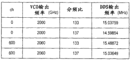
图4表示具体的计算例子。图4是表示从DDS电路4输出的基准频率的例子的表图。Fig. 4 shows a specific calculation example. FIG. 4 is a table diagram showing examples of reference frequencies output from the
如图4所示,例如在信道编号为0,分频比为133的情况下,基准频率(在图中记载为“DDS输出频率”)为15.03759MHz,即使是相同的信道编号0,在分频比137的情况下,为14.59854MHz。在本PLL电路中,如图2的分频比表所规定的那样,即使是相同的信道编号,由于温度的不同,最优的分频比也不同,因此,从DDS电路4输出的基准频率也不同。As shown in Figure 4, for example, when the channel number is 0 and the frequency division ratio is 133, the reference frequency (referred to as "DDS output frequency" in the figure) is 15.03759MHz. In the case of a frequency ratio of 137, it is 14.59854 MHz. In this PLL circuit, as stipulated in the frequency division ratio table in Figure 2, even for the same channel number, the optimal frequency division ratio is different due to the difference in temperature. Therefore, the reference frequency output from the
另外,DDS电路4的控制部件41根据计算出的基准频率的值,输出正弦波的数据,由D/A变换器变换为模拟信号,并经由滤波器将模拟正弦波信号作为基准频率信号输出到PLLIC2。In addition, the
由此,在DDS电路4中,能够与信道编号或使用温度对应地,根据寄生特性良好的分频比,生成基准频率信号。Accordingly, in the
[本PLL电路的寄生特性:图5][Parasitic characteristics of this PLL circuit: Figure 5]
接着,使用图5,说明本PLL电路的0~600信道的VCO1的输出寄生特性。图5是本PLL电路的VCO1的常温时的输出寄生特性的示意说明图。Next, the output spurious characteristics of the VCO1 of
如图5所示可以认为,在本PLL电路中,将对每个信道编号最优的分频比设定到PLLIC2,与之对应地改变DDS电路4的基准频率,由此,在全部信道编号中能够得到比图9的一般的PLL电路的寄生特性更良好的特性。As shown in Figure 5, it can be considered that in this PLL circuit, the optimal frequency division ratio for each channel number is set to PLLIC2, and the reference frequency of the
另外,在图5中,只表示出常温时,但低温时和高温时也成为比现有技术更良好的输出寄生特性。In addition, in FIG. 5 , only the normal temperature is shown, but the output parasitic characteristics are better than those of the prior art also at low temperature and high temperature.
[本PLL电路的适用例子:图6][Application example of this PLL circuit: Figure 6]
接着,使用图6,说明本PLL电路的适用例子。图6是适用了本PLL电路的数字控制PLL电路的结构框图。Next, an application example of this PLL circuit will be described using FIG. 6 . FIG. 6 is a block diagram of a digitally controlled PLL circuit to which this PLL circuit is applied.
如图6所示,适用了本PLL电路的数字控制PLL电路具备分频器11、A/D变换器12、相位比较器15、数字滤波器16、D/A变换器17,来代替图1的PLLIC2,VCO1、DDS电路14、模拟滤波器18与图1的PLL电路相同。As shown in FIG. 6, the digital control PLL circuit to which this PLL circuit is applied includes a
控制电路13与图1的PLL电路的控制电路3一样,具备温度传感器和分频比表,向A/D变换器12和D/A变换器17指示输出的定时这一点与图1的PLL电路不同。The
另外,数字控制PLL电路的控制电路13与图1的PLL电路的控制电路3一样,根据输入的信道编号和检测出的温度数据,从分频比表读取最优的分频比,设定到分频器11。In addition, the
同时,控制电路13向DDS电路14输出信道编号和分频比,在DDS电路14中,根据输入的信道编号和分频比,计算出基准频率,将正弦波数据输出到相位比较器15。At the same time, the
简单地说明上述结构的数字控制PLL电路的动作。The operation of the digitally controlled PLL circuit configured as described above will be briefly described.
由分频器11以从控制电路13指定的分频比(N)对VCO1的输出信号进行分频,按照指定的定时在A/D变换器12中进行A/D变换,并输入到相位比较器15。The output signal of VCO1 is frequency-divided by the
在相位比较器15中,对来自DDS电路14的基准频率和来自A/D变换器12的输出数据的相位进行比较,检测相位差,由数字滤波器16对相位差信号进行滤波,按照指定的定时在D/A变换器17中变换为模拟信号,在模拟滤波器18中进行频带限制,将控制电压施加到VCO1。In the
在适用了本PLL电路的数字控制PLL电路中,由于对分频器11和DDS电路14设定与温度和信道对应的最优的分频比,所以具有使VCO1的输出具有良好的寄生特性的效果。In the digital control PLL circuit to which this PLL circuit is applied, since the
[实施例的效果][Effect of the embodiment]
根据本发明的实施例的PLL电路,是以下这样的PLL电路,在控制电路3中设置温度传感器31,与温度对应地具备存储了每个信道的寄生特性最好的分频比的分频比表32,控制电路3根据从外部输入的信道编号、由温度传感器31检测出的温度数据,从分频比表32读取对应的分频比并设定到PLLIC2,将分频比和信道编号设定到DDS电路4,DDS电路4根据所设定的分频比和信道编号,计算出基准频率的值,生成基准频率信号,因此,具有以下的效果:无论在怎样的温度和信道下,都能够防止PLLIC2和DDS电路4中的寄生特性的恶化,能够使VCO输出的寄生特性良好。The PLL circuit according to the embodiment of the present invention is a PLL circuit in which a temperature sensor 31 is provided in the
另外,在本实施例中,与温度对应地具备设置在控制电路3中的分频比表,但在根据使用本PLL电路的环境而限制温度区域的情况下(例如常温等),也可以只存储与该温度区域对应的分频比。In addition, in this embodiment, the frequency division ratio table provided in the
另外,在因温度造成的特性的变动大的情况下,也可以增多温度区域的区分。In addition, when the variation of characteristics due to temperature is large, the division of temperature ranges may be increased.
本发明适用于能够提高寄生特性的PLL电路。The present invention is applicable to a PLL circuit capable of improving parasitic characteristics.
Claims (5)
Applications Claiming Priority (4)
| Application Number | Priority Date | Filing Date | Title |
|---|---|---|---|
| JP2009-141116 | 2009-06-12 | ||
| JP2009141116 | 2009-06-12 | ||
| JP2010-081506 | 2010-03-31 | ||
| JP2010081506A JP4850959B2 (en) | 2009-06-12 | 2010-03-31 | PLL circuit |
Publications (2)
| Publication Number | Publication Date |
|---|---|
| CN101924552A CN101924552A (en) | 2010-12-22 |
| CN101924552B true CN101924552B (en) | 2013-08-07 |
Family
ID=43305900
Family Applications (1)
| Application Number | Title | Priority Date | Filing Date |
|---|---|---|---|
| CN2010102029063A Active CN101924552B (en) | 2009-06-12 | 2010-06-11 | Pll circuit |
Country Status (3)
| Country | Link |
|---|---|
| US (1) | US8446192B2 (en) |
| JP (1) | JP4850959B2 (en) |
| CN (1) | CN101924552B (en) |
Families Citing this family (9)
| Publication number | Priority date | Publication date | Assignee | Title |
|---|---|---|---|---|
| JP4933635B2 (en) * | 2010-02-19 | 2012-05-16 | 日本電波工業株式会社 | PLL circuit |
| JP5863395B2 (en) * | 2011-11-02 | 2016-02-16 | 日本電波工業株式会社 | Oscillator |
| JP2013131985A (en) * | 2011-12-22 | 2013-07-04 | Anritsu Corp | Signal generation apparatus and signal generation method |
| EP3072240B1 (en) * | 2013-11-25 | 2019-06-12 | Nanowave Technologies Inc. | Digitally compensated phase locked oscillator |
| JP6720532B2 (en) * | 2016-01-06 | 2020-07-08 | セイコーエプソン株式会社 | Circuit devices, oscillators, electronic devices and mobile units |
| JP7009113B2 (en) * | 2017-08-23 | 2022-02-10 | 横河電機株式会社 | AC signal generator |
| DE102019201411B3 (en) | 2019-02-04 | 2020-06-25 | Infineon Technologies Ag | Synchronization of an integrated circuit with a sensor |
| US11621645B2 (en) * | 2020-06-04 | 2023-04-04 | Stmicroelectronics International N.V. | Methods and device to drive a transistor for synchronous rectification |
| JP7617801B2 (en) | 2021-04-07 | 2025-01-20 | 三菱電機株式会社 | Phase locked loop, transmitter, receiver, and method for controlling phase locked loop |
Citations (4)
| Publication number | Priority date | Publication date | Assignee | Title |
|---|---|---|---|---|
| CN1117672A (en) * | 1994-05-09 | 1996-02-28 | 日本电气株式会社 | PLL Frequency synthesizer |
| CN1169622A (en) * | 1996-06-28 | 1998-01-07 | 三菱电机株式会社 | frequency synthesizer |
| CN101093995A (en) * | 2006-06-19 | 2007-12-26 | 日本电波工业株式会社 | Pll oscillation circuit |
| CN101421929A (en) * | 2006-02-24 | 2009-04-29 | 日本电波工业株式会社 | PLL circuit |
Family Cites Families (10)
| Publication number | Priority date | Publication date | Assignee | Title |
|---|---|---|---|---|
| JPS6335017A (en) * | 1986-07-30 | 1988-02-15 | Japan Radio Co Ltd | Radio frequency stabilizing device |
| JP3344790B2 (en) * | 1993-10-28 | 2002-11-18 | アイコム株式会社 | Frequency synthesizer |
| JPH098551A (en) * | 1995-06-20 | 1997-01-10 | Fujitsu Ltd | High stable oscillation circuit |
| JPH0918336A (en) * | 1995-06-26 | 1997-01-17 | Yaesu Musen Co Ltd | Pll circuit control system |
| JP3395529B2 (en) * | 1996-06-28 | 2003-04-14 | 三菱電機株式会社 | Frequency synthesizer |
| JP2003069426A (en) | 2001-08-23 | 2003-03-07 | Matsushita Electric Ind Co Ltd | Frequency synthesizer |
| JP2004166179A (en) | 2002-09-17 | 2004-06-10 | Nec Kansai Ltd | Semiconductor integrated circuit device for radio communication |
| JP2007208367A (en) | 2006-01-31 | 2007-08-16 | Kenwood Corp | Synchronizing signal generating apparatus, transmitter, and control method |
| JP4824591B2 (en) * | 2007-02-05 | 2011-11-30 | 日本電波工業株式会社 | Synchronous sweep synthesizer |
| US7609122B2 (en) * | 2007-10-05 | 2009-10-27 | Silicon Storage Technology, Inc. | Method and system for calibration of a tank circuit in a phase lock loop |
-
2010
- 2010-03-31 JP JP2010081506A patent/JP4850959B2/en active Active
- 2010-06-11 CN CN2010102029063A patent/CN101924552B/en active Active
- 2010-06-11 US US12/801,498 patent/US8446192B2/en active Active
Patent Citations (4)
| Publication number | Priority date | Publication date | Assignee | Title |
|---|---|---|---|---|
| CN1117672A (en) * | 1994-05-09 | 1996-02-28 | 日本电气株式会社 | PLL Frequency synthesizer |
| CN1169622A (en) * | 1996-06-28 | 1998-01-07 | 三菱电机株式会社 | frequency synthesizer |
| CN101421929A (en) * | 2006-02-24 | 2009-04-29 | 日本电波工业株式会社 | PLL circuit |
| CN101093995A (en) * | 2006-06-19 | 2007-12-26 | 日本电波工业株式会社 | Pll oscillation circuit |
Non-Patent Citations (2)
| Title |
|---|
| JP特开平7-131343A 1995.05.19 |
| JP特开平9-8551A 1997.01.10 |
Also Published As
| Publication number | Publication date |
|---|---|
| JP2011019208A (en) | 2011-01-27 |
| CN101924552A (en) | 2010-12-22 |
| JP4850959B2 (en) | 2012-01-11 |
| US20100315137A1 (en) | 2010-12-16 |
| US8446192B2 (en) | 2013-05-21 |
Similar Documents
| Publication | Publication Date | Title |
|---|---|---|
| CN101924552B (en) | Pll circuit | |
| US5898325A (en) | Dual tunable direct digital synthesizer with a frequency programmable clock and method of tuning | |
| JP5694696B2 (en) | Frequency synthesizer device and modulation frequency displacement adjustment method | |
| US9215062B1 (en) | Low-noise flexible frequency clock generation from two fixed-frequency references | |
| US8170171B2 (en) | Communication semiconductor integrated circuit | |
| US7253691B2 (en) | PLL clock generator circuit and clock generation method | |
| KR100894236B1 (en) | PLL circuit, method of preventing interference of the PLL circuit and optical-disk apparatus having the PLL circuit | |
| CN116671015A (en) | Parameter error calibration for digital to time converter | |
| CN113692708B (en) | Generator and method for generating a controllable frequency | |
| US7283002B2 (en) | Phase locked loop with a modulator | |
| JP2008172512A (en) | Frequency synthesizer, phase-locked loop, and clock generation method | |
| CN101421929A (en) | PLL circuit | |
| CN102163971B (en) | PLL circuit | |
| CN105765867A (en) | Method and apparatus to calibrate frequency synthesizer | |
| WO2014109974A2 (en) | Method and apparatus for synthesis of wideband low phase noise radio frequency signals | |
| EP2890013A1 (en) | Phase locked loop and control method thereof | |
| KR20100039003A (en) | Apparatus and method for vco calibration using fast frequency comparision based on pahse manipulation | |
| JP2009004868A (en) | Spread spectrum clock generator | |
| TWI530084B (en) | A method for reducing spurious for a clock distribution system | |
| JP4499009B2 (en) | Frequency dividing circuit, clock generation circuit, and electronic device equipped with the same | |
| US10771071B1 (en) | Redundant DCO tuning with overlapping fractional regions | |
| JP2006262520A (en) | Clock generation circuit, PLL, and clock generation method | |
| JP2004312247A (en) | Local signal generator | |
| JP2021145285A (en) | Pll circuit and transmission device | |
| JP2018061117A (en) | Frequency synthesizer |
Legal Events
| Date | Code | Title | Description |
|---|---|---|---|
| C06 | Publication | ||
| PB01 | Publication | ||
| C10 | Entry into substantive examination | ||
| SE01 | Entry into force of request for substantive examination | ||
| C14 | Grant of patent or utility model | ||
| GR01 | Patent grant |