CN101401112B - Semiconductor device - Google Patents
Semiconductor device Download PDFInfo
- Publication number
- CN101401112B CN101401112B CN2007800085830A CN200780008583A CN101401112B CN 101401112 B CN101401112 B CN 101401112B CN 2007800085830 A CN2007800085830 A CN 2007800085830A CN 200780008583 A CN200780008583 A CN 200780008583A CN 101401112 B CN101401112 B CN 101401112B
- Authority
- CN
- China
- Prior art keywords
- circuit
- film
- battery
- antenna
- day line
- Prior art date
- Legal status (The legal status is an assumption and is not a legal conclusion. Google has not performed a legal analysis and makes no representation as to the accuracy of the status listed.)
- Expired - Fee Related
Links
Images


Classifications
-
- G—PHYSICS
- G06—COMPUTING; CALCULATING OR COUNTING
- G06K—GRAPHICAL DATA READING; PRESENTATION OF DATA; RECORD CARRIERS; HANDLING RECORD CARRIERS
- G06K19/00—Record carriers for use with machines and with at least a part designed to carry digital markings
- G06K19/06—Record carriers for use with machines and with at least a part designed to carry digital markings characterised by the kind of the digital marking, e.g. shape, nature, code
- G06K19/067—Record carriers with conductive marks, printed circuits or semiconductor circuit elements, e.g. credit or identity cards also with resonating or responding marks without active components
- G06K19/07—Record carriers with conductive marks, printed circuits or semiconductor circuit elements, e.g. credit or identity cards also with resonating or responding marks without active components with integrated circuit chips
- G06K19/077—Constructional details, e.g. mounting of circuits in the carrier
-
- H—ELECTRICITY
- H01—ELECTRIC ELEMENTS
- H01Q—ANTENNAS, i.e. RADIO AERIALS
- H01Q1/00—Details of, or arrangements associated with, antennas
- H01Q1/12—Supports; Mounting means
- H01Q1/22—Supports; Mounting means by structural association with other equipment or articles
- H01Q1/2208—Supports; Mounting means by structural association with other equipment or articles associated with components used in interrogation type services, i.e. in systems for information exchange between an interrogator/reader and a tag/transponder, e.g. in Radio Frequency Identification [RFID] systems
- H01Q1/2225—Supports; Mounting means by structural association with other equipment or articles associated with components used in interrogation type services, i.e. in systems for information exchange between an interrogator/reader and a tag/transponder, e.g. in Radio Frequency Identification [RFID] systems used in active tags, i.e. provided with its own power source or in passive tags, i.e. deriving power from RF signal
-
- G—PHYSICS
- G06—COMPUTING; CALCULATING OR COUNTING
- G06K—GRAPHICAL DATA READING; PRESENTATION OF DATA; RECORD CARRIERS; HANDLING RECORD CARRIERS
- G06K19/00—Record carriers for use with machines and with at least a part designed to carry digital markings
- G06K19/06—Record carriers for use with machines and with at least a part designed to carry digital markings characterised by the kind of the digital marking, e.g. shape, nature, code
- G06K19/067—Record carriers with conductive marks, printed circuits or semiconductor circuit elements, e.g. credit or identity cards also with resonating or responding marks without active components
- G06K19/07—Record carriers with conductive marks, printed circuits or semiconductor circuit elements, e.g. credit or identity cards also with resonating or responding marks without active components with integrated circuit chips
- G06K19/0701—Record carriers with conductive marks, printed circuits or semiconductor circuit elements, e.g. credit or identity cards also with resonating or responding marks without active components with integrated circuit chips at least one of the integrated circuit chips comprising an arrangement for power management
- G06K19/0702—Record carriers with conductive marks, printed circuits or semiconductor circuit elements, e.g. credit or identity cards also with resonating or responding marks without active components with integrated circuit chips at least one of the integrated circuit chips comprising an arrangement for power management the arrangement including a battery
-
- G—PHYSICS
- G06—COMPUTING; CALCULATING OR COUNTING
- G06K—GRAPHICAL DATA READING; PRESENTATION OF DATA; RECORD CARRIERS; HANDLING RECORD CARRIERS
- G06K19/00—Record carriers for use with machines and with at least a part designed to carry digital markings
- G06K19/06—Record carriers for use with machines and with at least a part designed to carry digital markings characterised by the kind of the digital marking, e.g. shape, nature, code
- G06K19/067—Record carriers with conductive marks, printed circuits or semiconductor circuit elements, e.g. credit or identity cards also with resonating or responding marks without active components
- G06K19/07—Record carriers with conductive marks, printed circuits or semiconductor circuit elements, e.g. credit or identity cards also with resonating or responding marks without active components with integrated circuit chips
- G06K19/0723—Record carriers with conductive marks, printed circuits or semiconductor circuit elements, e.g. credit or identity cards also with resonating or responding marks without active components with integrated circuit chips the record carrier comprising an arrangement for non-contact communication, e.g. wireless communication circuits on transponder cards, non-contact smart cards or RFIDs
-
- G—PHYSICS
- G06—COMPUTING; CALCULATING OR COUNTING
- G06K—GRAPHICAL DATA READING; PRESENTATION OF DATA; RECORD CARRIERS; HANDLING RECORD CARRIERS
- G06K19/00—Record carriers for use with machines and with at least a part designed to carry digital markings
- G06K19/06—Record carriers for use with machines and with at least a part designed to carry digital markings characterised by the kind of the digital marking, e.g. shape, nature, code
- G06K19/067—Record carriers with conductive marks, printed circuits or semiconductor circuit elements, e.g. credit or identity cards also with resonating or responding marks without active components
- G06K19/07—Record carriers with conductive marks, printed circuits or semiconductor circuit elements, e.g. credit or identity cards also with resonating or responding marks without active components with integrated circuit chips
- G06K19/077—Constructional details, e.g. mounting of circuits in the carrier
- G06K19/07749—Constructional details, e.g. mounting of circuits in the carrier the record carrier being capable of non-contact communication, e.g. constructional details of the antenna of a non-contact smart card
- G06K19/07766—Constructional details, e.g. mounting of circuits in the carrier the record carrier being capable of non-contact communication, e.g. constructional details of the antenna of a non-contact smart card comprising at least a second communication arrangement in addition to a first non-contact communication arrangement
- G06K19/07767—Constructional details, e.g. mounting of circuits in the carrier the record carrier being capable of non-contact communication, e.g. constructional details of the antenna of a non-contact smart card comprising at least a second communication arrangement in addition to a first non-contact communication arrangement the first and second communication means being two different antennas types, e.g. dipole and coil type, or two antennas of the same kind but operating at different frequencies
-
- H—ELECTRICITY
- H01—ELECTRIC ELEMENTS
- H01L—SEMICONDUCTOR DEVICES NOT COVERED BY CLASS H10
- H01L21/00—Processes or apparatus adapted for the manufacture or treatment of semiconductor or solid state devices or of parts thereof
- H01L21/70—Manufacture or treatment of devices consisting of a plurality of solid state components formed in or on a common substrate or of parts thereof; Manufacture of integrated circuit devices or of parts thereof
- H01L21/77—Manufacture or treatment of devices consisting of a plurality of solid state components or integrated circuits formed in, or on, a common substrate
- H01L21/78—Manufacture or treatment of devices consisting of a plurality of solid state components or integrated circuits formed in, or on, a common substrate with subsequent division of the substrate into plural individual devices
- H01L21/82—Manufacture or treatment of devices consisting of a plurality of solid state components or integrated circuits formed in, or on, a common substrate with subsequent division of the substrate into plural individual devices to produce devices, e.g. integrated circuits, each consisting of a plurality of components
- H01L21/822—Manufacture or treatment of devices consisting of a plurality of solid state components or integrated circuits formed in, or on, a common substrate with subsequent division of the substrate into plural individual devices to produce devices, e.g. integrated circuits, each consisting of a plurality of components the substrate being a semiconductor, using silicon technology
-
- H—ELECTRICITY
- H01—ELECTRIC ELEMENTS
- H01Q—ANTENNAS, i.e. RADIO AERIALS
- H01Q7/00—Loop antennas with a substantially uniform current distribution around the loop and having a directional radiation pattern in a plane perpendicular to the plane of the loop
Landscapes
- Engineering & Computer Science (AREA)
- Computer Hardware Design (AREA)
- Microelectronics & Electronic Packaging (AREA)
- Physics & Mathematics (AREA)
- General Physics & Mathematics (AREA)
- Theoretical Computer Science (AREA)
- Computer Networks & Wireless Communication (AREA)
- Condensed Matter Physics & Semiconductors (AREA)
- Manufacturing & Machinery (AREA)
- Power Engineering (AREA)
- Near-Field Transmission Systems (AREA)
- Semiconductor Integrated Circuits (AREA)
- Charge And Discharge Circuits For Batteries Or The Like (AREA)
- Thin Film Transistor (AREA)
Abstract
The present invention provides a battery as a power supply for supplying power in the RFID, and another antenna for charging the battery, in addition to an antenna which transmits and receives individual information to and from outside as a means for supplying power to the battery.
Description
Technical field
The present invention relates to semiconductor devices.Especially, the present invention relates to transmit and receive data and receive the semiconductor devices of electric power by radiowave.In addition, the present invention relates to communication system, wherein this communication system is used semiconductor devices by radiowave, is sent data and from the antenna of this semiconductor devices receive data and reader/writer and to antenna and the charger of this semiconductor devices power supply to this semiconductor devices.
Note that in this manual semiconductor devices refers to can be by all device that use characteristic of semiconductor to move.
Background technology
Recently, use is noted widely such as the individual identification technology of the electromagnetic radiowave that is used for radio communication.Especially, as the semiconductor devices that transmits data by radio communication, use the individual identification technology of RFID (radio-frequency (RF) identification) label to be noted widely.RFID label (hereinafter referred to as RFID) also is called IC (integrated circuit) label, IC chip, RF label, wireless identification tag or electronic tag.Use the individual identification technology of RFID to be used for the production, management etc. of individual articles, and be supposed to for the personal verification.
Whether be included among the RFID or whether power supply provides from the outside according to power supply, RFID can be divided into two types: active type RFID, and it can send the radiowave that comprises the information on the RFID; With passive RFID, it is used to electric power from outside radiowave or radiowave (carrier wave) and drives that (active type RFID is referring to list of references 1: day patented claim No.2005-316724 of the present disclosure; Passive RFID is referring to the translator of Japanese of list of references 2:PCT international application No.2006-503376).Wherein, active type RFID has and wherein includes for the power supply that drives RFID and the structure that battery provides as power supply.In addition, passive RFID has wherein by the electric power that uses external wireless electric wave (carrier wave) and produces structure for the power supply that drives RFID, therefore realizes not having the structure of battery.
Figure 31 is the block diagram that the concrete structure of active type RFID is shown.In the active type RFID3100 of Figure 31, demodulator circuit 3105 and amplifier 3106 in signal processing circuit 3102 are inputted the signal of communication that is received by antenna circuit 3101.Usually, using ASK modulation, PSK modulation etc. to send signal of communication after having processed carrier wave such as 13.56MHz carrier wave or 915MHz carrier wave.Here, figure 31 illustrates example as the 13.56MHz carrier wave of signal of communication.In Figure 31, need to be as the clock signal of benchmark for the treatment of signal, and here with the 13.56MHz carrier wave as clock.Amplifier 3106 amplifies the 13.56MHz carrier wave, and it is provided to logical circuit 3107 as clock.In addition, carry out demodulation by 3105 pairs of signals of communication of modulating through signal of communication or the process PSK of ASK modulation of demodulator circuit.Also the signal of demodulation being sent to logical circuit 3107 analyzes.To send to memorizer control circuit 3108 by the signal that logical circuit 3107 is analyzed, and based on this, memorizer control circuit 3108 control store circuit 3109, and the data of storage in the memory circuitry 3109 are taken out and send to logical circuit 3110.The signal that is stored in the memory circuitry 3109 is amplified by amplifier 3111 through being processed then by logical circuit 3110 codings, so modulation circuit 3112 uses this signal modulated carrier.Here, provide power supply among Figure 31 by the battery 3103 that provides in the signal processing circuit outside through power circuits 3104.Power circuit 3104 is to supply electric power such as amplifier 3106, demodulator circuit 3105, logical circuit 3107, memorizer control circuit 3108, memory circuitry 3109, logical circuit 3110, amplifier 3111, modulation circuits 3112.So, active type RFID operation.
Figure 32 is the block diagram that the concrete structure of passive RFID is shown.In the passive RFID3200 of Figure 32, demodulator circuit 3205 and amplifier 3206 in signal processing circuit 3202 are inputted the signal of communication that is received by antenna circuit 3201.Usually, using ASK modulation, PSK modulation etc. to send signal of communication after having processed carrier wave such as 13.56MHz carrier wave or 915MHz carrier wave.Here, figure 32 illustrates example as the 13.56MHz carrier wave of signal of communication.In Figure 32, need to be as the clock signal of benchmark for the treatment of signal, and here with the 13.56MHz carrier wave as clock.Amplifier 3206 amplifies the 13.56MHz carrier wave, and it is provided to logical circuit 3207 as clock.In addition, carry out demodulation by 3205 pairs of signals of communication of modulating through signal of communication or the process PSK of ASK modulation of demodulator circuit.Also the signal of demodulation being sent to logical circuit 3207 analyzes.To send to memorizer control circuit 3208 by the signal that logical circuit 3207 is analyzed, and based on this, memorizer control circuit 3208 control store circuit 3209, and the data of storage in the memory circuitry 3209 are taken out and send to logical circuit 3210.The signal that is stored in the memory circuitry 3209 is amplified by amplifier 3211 through being processed then by logical circuit 3210 codings, so modulation circuit 3212 uses this signal modulated carrier.On the other hand, the signal of communication of inputting to rectification circuit 3203 is rectified, and is imported into power circuit 3204.Power circuit 3204 is to supply electric power such as amplifier 3206, demodulator circuit 3205, logical circuit 3207, memorizer control circuit 3208, memory circuitry 3209, logical circuit 3210, amplifier 3211, modulation circuits 3212.So, passive RFID operation.
Summary of the invention
Yet, as shown in figure 31, have in the situation about providing for the semiconductor devices of the active type RFID of the battery that drives, there is such problem, namely according to the sending and receiving of individual information and the needed radio wave intensity of sending and receiving is set and consuming cells electric power in time, to such an extent as to can not produce at last the needed electric power of sending and receiving individual information.Therefore, there is such problem, namely produced to the affirmation of the residual capacity of battery with to the replacement of battery, have the semiconductor devices that provides for the active type RFID of the battery that drives to continue to use.
In addition, shown in figure 32, have in the situation about producing by the electric power that uses external wireless electric wave (carrier wave) for the semiconductor devices of the passive RFID of the power supply that drives, there is such problem, the electric power that namely is difficult to over long distances sending and receiving signal and guarantees the needed transmission radiowave of sending and receiving is so be difficult to realize good sending and receiving state.Therefore, there is such problem, namely from being limited shortlyer as the antenna of the reader/writer of supply unit to the distance in the place of the electric power that enough external wireless electric wave (carrier wave) is provided, so that produce semiconductor devices for the passive RFID of the power supply that drives with having by the electric power that uses external wireless electric wave (carrier wave).
Consider the problem of front, the semiconductor devices that the purpose of this invention is to provide a kind of RFID of comprising, wherein individual information can be sent out and receive, even and do not exist with the battery that is used for driving power fail in time relevant to battery remaining power affirmation and the situation of the replacement of battery under when not providing the electric power of enough external wireless electric wave (carrier wave) to the power supply that is used for driving, the sending and receiving of individual information also can remain on good state.
In order to address the above problem, the invention provides battery (being also referred to as secondary cell) as the power supply that is used for providing electric power among the RFID.Except sending to the outside and receive from the outside the antenna of individual information, the present invention also provides as another antenna to the battery charging of being used for to the device of battery supplied electric power.Hereinafter, shown concrete structure of the present invention.
A feature of the present invention is a kind of semiconductor devices, and it comprises: the first day line circuit; The second day line circuit; Signal processing circuit; And battery, wherein said first day line circuit is by strengthening antenna receiving signal and sending the signal that is used for sending the data that are stored in described signal processing circuit; And described second day line circuit receives the signal that is used for described battery charging.
Another feature of the present invention is a kind of semiconductor devices, and it comprises: the first day line circuit; The second day line circuit; Signal processing circuit; And battery, wherein said first day line circuit receives signal and is used for the signal that transmission is stored in the data of described signal processing circuit to the reader/writer transmission from reader/writer; And described second day line circuit receives the signal that is used for described battery charging from the charger that comprises antenna circuit.
Another feature of the present invention is a kind of semiconductor devices, and it comprises: the first day line circuit; The second day line circuit; Strengthen antenna; Signal processing circuit; And battery, wherein said first day line circuit is by described enhancing antenna receiving signal and send the signal that is used for sending the data that are stored in described signal processing circuit; And described second day line circuit is used for signal to described battery charging by described enhancing antenna reception.
Another feature of the present invention is a kind of semiconductor devices, and it comprises: the first day line circuit; The second day line circuit; Strengthen antenna; Signal processing circuit; And battery, wherein said first day line circuit receives signal and sends the signal that is used for sending the data that are stored in described signal processing circuit; And described second day line circuit is used for signal to described battery charging by described enhancing antenna reception.
Another feature of the present invention is a kind of semiconductor devices, and it comprises: the first day line circuit; The second day line circuit; Strengthen antenna; Signal processing circuit; And battery, wherein said first day line circuit receives signal and sends for the signal that sends the data that are stored in described signal processing circuit by described enhancing antenna; And described second day line circuit receives the signal that is used for described battery charging by described enhancing antenna from the charger that comprises antenna circuit.
Another feature of the present invention is a kind of semiconductor devices, and it comprises: the first day line circuit; The second day line circuit; Strengthen antenna; Signal processing circuit; And battery, wherein said first day line circuit receives signal and is used for the signal that transmission is stored in the data of described signal processing circuit to the reader/writer transmission from reader/writer by described enhancing antenna; And described second day line circuit receives the signal that is used for described battery charging.
Another feature of the present invention is a kind of semiconductor devices, and it comprises: the first day line circuit; The second day line circuit; Strengthen antenna; Signal processing circuit; And battery, wherein said first day line circuit receives signal and is used for the signal that transmission is stored in the data of described signal processing circuit to the reader/writer transmission from reader/writer; And described second day line circuit receives the signal that is used for described battery charging by described enhancing antenna from the charger that comprises antenna circuit.
Another feature of the present invention is a kind of semiconductor devices, and it comprises: the first day line circuit; The second day line circuit; Strengthen antenna; Signal processing circuit; And battery, wherein said first day line circuit receives signal and is used for the signal that transmission is stored in the data of described signal processing circuit to the reader/writer transmission from reader/writer by described enhancing antenna; And described second day line circuit receives the signal that is used for described battery charging by described enhancing antenna from the charger that comprises antenna circuit.
Described battery of the present invention can be for being included in the power circuit power supply in the described signal processing circuit.
Described first day line circuit of the present invention and described second day line circuit can be by the method sending and receiving radio signals of electromagnetic induction.
In the present invention, can satisfy relational expression 0.5m<M<1.5m, the signal frequency that is wherein received by described first day line circuit is made as M (M is positive number), and the signal frequency that is received by described second day line circuit is made as m (m is positive number).
Battery of the present invention can be lithium battery, Ni-MH battery, nickel-cadmium battery or capacitor.
Semiconductor devices of the present invention comprises battery.Therefore, similar with conventional semiconductor devices, semiconductor devices of the present invention can prevent the situation of the power shortage that be used for sending and receiving individual information relevant with battery decline in time.In addition, semiconductor devices of the present invention has the antenna that receives for to battery powered signal.Therefore, when using the electric power of outside radiowave, battery can be in the situation that semiconductor devices directly be connected with charger is recharged.Therefore, can under not producing the situation of the affirmation of battery remaining power and the replacement of battery (as active type RFID), continue to use semiconductor devices of the present invention.In addition, the electric power that drives RFID is kept in the battery all the time, thereby can obtains to move the enough electric power of RFID, and can expand the communication distance between reader/writer and the RFID.
Description of drawings
Fig. 1 is the schematic diagram of structure that the semiconductor devices of embodiment 1 is shown.
Fig. 2 is the schematic diagram of structure that the semiconductor devices of embodiment 1 is shown.
Fig. 3 A~Fig. 3 E is the view of structure that the semiconductor devices of embodiment 1 is shown respectively.
Fig. 4 A and Fig. 4 B are the schematic diagram of structure that the semiconductor devices of embodiment 1 is shown respectively.
Fig. 5 is the schematic diagram of structure that the semiconductor devices of embodiment 1 is shown.
Fig. 6 is the schematic diagram of structure that the semiconductor devices of embodiment 1 is shown.
Fig. 7 is the view of structure that the semiconductor devices of embodiment 1 is shown.
Fig. 8 is the view of structure that the semiconductor devices of embodiment 1 is shown.
Fig. 9 is the view of structure that the semiconductor devices of embodiment 1 is shown.
Figure 10 is the view of structure that the semiconductor devices of embodiment 1 is shown.
Figure 11 A and Figure 11 B are the views of structure that the semiconductor devices of embodiment 2 is shown respectively.
Figure 12 is the schematic diagram of structure that the semiconductor devices of embodiment 2 is shown.
Figure 13 is the schematic diagram of structure that the semiconductor devices of embodiment 2 is shown.
Figure 14 is the schematic diagram of structure that the semiconductor devices of embodiment 2 is shown.
Figure 15 is the schematic diagram of structure that the semiconductor devices of embodiment 2 is shown.
Figure 16 is the view of structure that the semiconductor devices of embodiment 2 is shown.
Figure 17 is the view of structure that the semiconductor devices of embodiment 2 is shown.
Figure 18 is the view of structure that the semiconductor devices of embodiment 2 is shown.
Figure 19 A~Figure 19 D is the schematic diagram of structure that the semiconductor devices of embodiment 3 is shown.
Figure 20 A~Figure 20 C is the schematic diagram of structure that the semiconductor devices of embodiment 3 is shown.
Figure 21 A and Figure 21 B are the schematic diagram of structure that the semiconductor devices of embodiment 3 is shown.
Figure 22 A and Figure 22 B are the schematic diagram of structure that the semiconductor devices of embodiment 3 is shown.
Figure 23 A and Figure 23 B are the schematic diagram of structure that the semiconductor devices of embodiment 3 is shown.
Figure 24 A~Figure 24 D is the schematic diagram of structure that the semiconductor devices of embodiment 4 is shown.
Figure 25 A and Figure 25 B are the schematic diagram of structure that the semiconductor devices of embodiment 4 is shown.
Figure 26 A and Figure 26 B are the schematic diagram of structure that the semiconductor devices of embodiment 4 is shown.
Figure 27 A and Figure 27 B are the schematic diagram of structure that the semiconductor devices of embodiment 4 is shown.
Figure 28 A and Figure 28 B are the schematic diagram of structure that the semiconductor devices of embodiment 4 is shown.
Figure 29 A and Figure 29 B are the schematic diagram of structure that the semiconductor devices of embodiment 4 is shown.
Figure 30 A~Figure 30 E is the view that the pattern of embodiment is shown respectively.
Figure 31 is the schematic diagram that traditional structure is shown.
Figure 32 is the schematic diagram that traditional structure is shown.
Figure 33 A~Figure 33 F is the schematic diagram of structure that the semiconductor devices of embodiment 5 is shown respectively.
Embodiment
Hereinafter, embodiments of the present invention will be described with reference to the drawings.Yet the present invention can realize in various patterns.Easily know for those skilled in the art, can carry out various variations to pattern of the present invention and details in the situation that do not break away from the spirit and scope of the invention.Therefore, the present invention is not considered to be subject to the description of following embodiment.Note that below in the different accompanying drawings of structure of the present invention of explanation uses identical label to represent identical assembly usually.
(embodiment 1)
The semiconductor devices that is used as RFID of the present invention is described with reference to the block diagram shown in Fig. 1 and Fig. 2.
The RFID100 of Fig. 1 comprises first day line circuit 101, second day line circuit 102, signal processing circuit 103 and battery 104.Signal processing circuit 103 comprises the first rectification circuit 105, power circuit 106, the second rectification circuit 107, demodulator circuit 108, amplifier 109, logical circuit 110, memorizer control circuit 111, memory circuitry 112, logical circuit 113, amplifier 114 and modulation circuit 115.
In addition, Fig. 2 shows block diagram, and wherein first day line circuit 101 receives signal to reader/writer 201 transmitted signals and from reader/writer 201, and second day line circuit 102 receives signal from charger 202.In Fig. 2, input the signal that is received by first day line circuit 101 to power circuit 106 by the first rectification circuit 105.In Fig. 2, input the signal that is received by second day line circuit 102 to battery 104 by the second rectification circuit 107, and in due course 106 power supplies from battery 104 to power circuit.
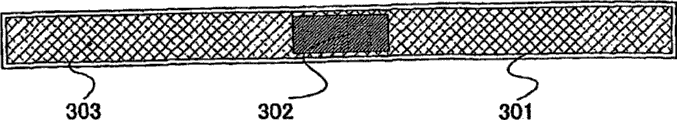
Note that for each the antenna pattern in first day line circuit 101 and the second day line circuit 102 and be not particularly limited.For example, as shown in Figure 3A, can use antenna 303 wherein to cover the structure of the periphery of the signal processing circuit 302 on the substrate 301.In addition, shown in Fig. 3 B, can use signal processing circuit 302 wherein to be arranged to be placed on structure on the antenna 303 that is formed on circlewise on the substrate 301.In addition, shown in Fig. 3 C, can use the shape according to the antenna 303 that is used for the reception frequency electromagnetic waves of the signal processing circuit 302 on substrate 301.In addition, shown in Fig. 3 D, can use 180 degree omnidirectional antennas 303 (can be similar to from any direction and receive signal) according to the signal processing circuit 302 on substrate 301.In addition, shown in Fig. 3 E, can use the shape that extends to bar-shaped antenna 303 according to the signal processing circuit 302 on substrate 301.In addition, be not particularly limited for being connected between the antenna in signal processing circuit 103 and first day line circuit 101 and the second day line circuit 102.For example, antenna 303 is connected with signal processing circuit and is connected by wire-bonded or bump bonding.Interchangeable, signal processing circuit 302 can be attached on the antenna 303, wherein signal processing circuit 302 is the chips that have at its whole lip-deep electrode.In the method, by using ACF (anisotropic conductive film), signal processing circuit 302 and antenna 303 can adhere to mutually.In this embodiment, adopt the shape shown in Fig. 3 B as each the shape in first day line circuit 101 and the second day line circuit 102.That is to say, shown in Fig. 4 A, in first day line circuit 101 and the second day line circuit 102 each is described to have the structure that comprises antenna 401 and resonant capacitor 402, and antenna circuit 403 refers to the combination of antenna 401 and resonant capacitor 402.
In addition, the first rectification circuit 105 and the second rectification circuit 107 can be the circuit that the AC signal of the electromagnetic wave induction that wherein will be received by first day line circuit 101 and second day line circuit 102 is converted to direct current signal.For example, shown in Fig. 4 B, rectification circuit 407 can comprise diode 404, diode 405 and smmothing capacitor 406.
Note that the reader/writer 201 among Fig. 2 is described with reference to Figure 5.Reader/writer 500 among Fig. 5 comprises receiving unit 501, transmitting portion 502, control section 503, interface section 504 and antenna circuit 505.Control section 503 control receiving unit 501 and transmitting portions 502 are to export data processing instructions and data processed result by the control via the more high-grade device 506 of interface section 504.502 pairs of data processing instructions that are sent to RFID100 of transmitting portion are modulated, and it is exported from antenna circuit 505 as electromagnetic wave.501 pairs of signals that received by antenna circuit 505 of receiving unit carry out demodulation, and it is outputed to control section 503 as data processed result.
In this embodiment, the antenna circuit 505 of the reader/writer shown in Fig. 5 500 is connected to antenna 507 and the resonant capacitor 508 that receiving unit 501 and transmitting portion 502 and each antenna circuit 505 comprise the parallel resonant circuit of formation LC.Antenna circuit 505 is received in the antenna circuit 505 by from the electromotive force of RFID100 as the induction of signal of electric signal output in receive data.In addition, when sending data, electric current flows through antenna circuit 505, and antenna circuit 505 is to the RFID100 transmitted signal.
Note that the charger 202 among Fig. 2 is described with reference to Figure 6.Charger 600 among Fig. 6 comprises transmission control section 601 and antenna circuit 602.601 pairs of control sections of transmission are sent to the electric signal that is used for charging of RFID100 and modulate, and the signal that is used for charging is sent out from antenna circuit 602.
In this embodiment, the antenna circuit 602 of the charger 600 shown in Fig. 6 is connected to and sends control section 601, and comprises antenna 603 and the resonant capacitor 604 that forms the parallel resonant circuit of LC.In antenna circuit 602, electric current flows through antenna circuit 602, and when sending data, sends the signal that is used for the RFID100 charging by antenna 603.
Note that in Fig. 1, first day line circuit 101 and second day line circuit 102 can be stacked on the substrate identical with signal processing circuit 103, and perhaps can be used as exterior antenna provides.
In addition, in this embodiment, the signal that is received by first day line circuit 101 and second day line circuit 102 preferably realizes that by the electromagnetic induction method signal communicates by letter.Therefore, the RFID100 in Fig. 1 and Fig. 2 preferably has the structure that comprises the first coil antenna circuit 101 and the second coil antenna circuit 102.For example, Fig. 7 shows the position relationship of first day line circuit and second day line circuit, and the antenna pattern in comprising the semiconductor devices of RFID.Fig. 7 shows a kind of structure, and the first coil antenna circuit 701 and the second coil antenna circuit 702 are provided at respectively on the front surface and rear surface of RFID700 in this structure, and receives the signal from the charger antenna in this structure.
Among Fig. 7, when with the antenna circuit 704 that sends the charger that control section 703 is connected among coil antenna 705 during near the second day line circuit 702 of RFID, the coil antenna 705 generation AC magnetic field of the antenna circuit 704 from charger.AC magnetic field is through the second coil antenna circuit 702 among the RFID700, so owing to (between an end and its other end of antenna) between the terminal of the second coil antenna circuit 702 of electromagnetic induction in RFID700 produced electromotive force.Battery among the RFID700 can be by this electromotive force charging.Note that as shown in Figure 8, even when RFID800 is applied, is provided at the front surface of the substrate among the RFID800 and the second day line circuit 801 that is used for charging on the rear surface and also can charges from charger.In addition as shown in Figure 9, RFID900 can have such structure, and first day line circuit 901 and second day line circuit 902 can be arranged on the same substrate side by side in this structure, and receives the signal from the antenna circuit 704 of charger.
The signal frequency that note that sending and receiving between first day line circuit 101 and reader/writer 201 is by standardized 125kHz, 13.56MHz, 915MHz, 2.45GHz etc. such as ISO.Certainly, the signal frequency of sending and receiving is not limited to this between first day line circuit 101 and reader/writer 201, and for example, can use following any one: the submillimeter wave of 300GHz~3THz; The millimeter wave of 30GHz~300GHz; The microwave of 3GHz~30GHz; The ultrashort wave (USW) of 300MHz~3GHz; The very short wave (VSW) of 30MHz~300MHz; The shortwave of 3MHz~30MHz; The medium wave of 300KHz~3MHz; The long wave of 30KHz~300KHz; And the myriameter waves of 3KHz~30KHz.In addition, the signal of sending and receiving is the signal of wherein having modulated carrier wave between first day line circuit 101 and reader/writer 201.The modulator approach of carrier wave can be analog-modulated or Digital Modulation, perhaps can be in amplitude modulation(PAM), phase-modulation, frequency modulation (PFM) and the spread-spectrum any one.Preferably, can use amplitude modulation(PAM) or frequency modulation (PFM).
Please note, when the signal frequency at sending and receiving between second day line circuit 102 and the charger 202 is made as m (m is positive number) and the signal frequency of sending and receiving is made as M (M is positive number) between first day line circuit 101 and reader/writer 201, the preferred frequency that satisfies relational expression 0.5m<M<1.5m and m ≠ M of using.In the time of in the signal frequency that is input to second day line circuit 102 is arranged on above-mentioned scope, can realize design in the situation of the shape of not obvious change first day line circuit 101 and second day line circuit 102, this is preferred.
Please note, can power to the power circuit 106 among Fig. 1 and Fig. 2 by dual mode: a kind of is such power supply, wherein this power supply is produced so that is rectified in the first rectification circuit 105 with the similar carrier signal of the passive RFID that describes in conventional example, and the power supply that drives each circuit of signal processing circuit 103 produces by power circuit 106; Another kind is such power supply, and wherein this power supply is produced so that battery 104 is charged by the battery-charge signal from second day line circuit 102 input through the second rectification circuit 107, and the electric power that fills in battery 104 is provided.When the communication distance overtime can not obtain from the first day line circuit 101 of RFID100 the electric power that fills in battery 104 to be offered power circuit 106 in the situation of enough electric power.
The example of the power circuit among Fig. 1 and Fig. 2 is described with reference to Figure 10.Power circuit comprises reference voltage circuit and buffer amplifier.Reference voltage circuit comprises resistor 1001 and diode-connected transistor 1002 and 1003, and the reference voltage that equates with transistorized twice VGS of generation.Buffer amplifier comprises: the difference channel that comprises transistor 1005 and 1006; The current mirroring circuit that comprises transistor 1007 and 1008; And the commonsource amplifier that comprises current source resistor 1004, transistor 1009 and resistor 1010.
In the power circuit shown in Figure 10, when the electric current that flows through from output terminal is larger, be supplied to the electric current of transistor 1009 less, otherwise when the electric current that flows through from output terminal hour, be supplied to the electric current of transistor 1009 larger.Therefore, executable operations is so that flow through the current constant of transistor 1010.In addition, the current potential of output terminal and reference voltage circuit have almost identical value.Here, show the power circuit that comprises reference voltage circuit and buffer amplifier; Yet, the invention is not restricted to the power circuit among Figure 10, it can also be other circuit.
Note that in this manual, battery represents to recover by charging the battery of its continuous service time.Note that and preferably use the sheet battery as this battery.For example, this battery can be by using lithium battery, preferably uses the lithium polymer battery, lithium ion battery etc. of gel-like electrolyte and be made less.Certainly, can use any battery as this battery as long as it is chargeable battery, and can use can charging and discharging battery such as Ni-MH battery or nickel-cadmium battery, perhaps can use capacitor that has high capacitance etc.
Next, the operation that sends data from reader/writer 201 to RFID100 shown in Fig. 1 and Fig. 2 is described below.By the first rectification circuit 105 signal that first day line circuit 101 receives is carried out half-wave rectification, then to its smoothing.To the voltage of power circuit 106 inputs by the first rectification circuit 105 half-wave rectification and smoothing.Power circuit provides stable voltage to the first rectification circuit 105, power circuit 106, the second rectification circuit 107, demodulator circuit 108, amplifier 109, logical circuit 110, memorizer control circuit 111, memory circuitry 112, logical circuit 113, amplifier 114 and modulation circuit 115.
In addition, the signal that is received by first day line circuit 101 to logical circuit 110 input by amplifier 109 is as clock signal.In addition, carry out demodulation and it is input to logical circuit 110 as data by 108 pairs of signals from 101 inputs of first day line circuit of demodulator circuit.
In logical circuit 110, the data that decoding is inputted.Reader/writer 201 sends this data after by distorting lens code (deformation mirror code), NRZ-L code etc. data being encoded, and by logical circuit 110 it is decoded.The data of decoding are sent to memorizer control circuit 111; Therefore, with the data reading that is stored in the memory circuitry 112.Even memory circuitry 112 need to be also can save data when power cut Nonvolatile memory circuit, and use mask rom etc.
In addition, when reader/writer 201 receives the data of storage in the memory circuitry 112 among the RFID100 shown in Fig. 1 and Fig. 2, following executable operations.The signal that receives by 105 pairs of first day line circuits of the first rectification circuit 101 carries out half-wave rectification, then to its smoothing.To the voltage of power circuit 106 inputs by the first rectification circuit 105 half-wave rectification and smoothing.Power circuit provides stable voltage to the first rectification circuit 105, power circuit 106, the second rectification circuit 107, demodulator circuit 108, amplifier 109, logical circuit 110, memorizer control circuit 111, memory circuitry 112, logical circuit 113, amplifier 114 and modulation circuit 115.
In addition, input the AC signal that is received by first day line circuit 101 to logical circuit 110 by amplifier 109, and the actuating logic computing.Then, use the signal from logical circuit 110 to come control store control circuit 111, and be invoked at the data of storage in the memory circuitry 112.Process the data of calling from memory circuitry 112 by logical circuit 113, amplify these data by amplifier 114, then, operation modulation circuit 115.Although process according to the standard implementation data such as ISO14443, ISO15693 or ISO18000, can adopt the disposal system except these standards, as long as the compatibility of assurance and reader/writer.
When modulation circuit 115 operation, the impedance of first day line circuit 101 changes.Therefore, changed by the signal of the reader/writer 201 that first day line circuit 101 affects.When reader/writer reads this change, can know the data of storage in the memory circuitry 112 among the RFID100.This modulator approach is called the load-modulate method.
Next, the operation of being charged by charger 202 is described below in the RFID100 shown in Fig. 1 and Fig. 2.The signal that receives by the 107 pairs of second day line circuits of the second rectification circuit carries out half-wave rectification and to its smoothing.To be stored in the battery 104 by the voltage of the second rectification circuit 107 half-wave rectification and smoothing temporarily.The electric power that provides to power circuit 106 is provided the electric power of preserving in the battery 104.Note that when the signal that provided by the first day line circuit can be provided but when being used for power shortage to the reader/writer transmitted signal, can use to be provided with the structure that determines whether to be provided by battery the circuit of electric power.
Next, show the example of the top view of the RFID100 shown in Fig. 1.According to function and the size of RFID100, RFID100 can have such layout, and first day line circuit, second day line circuit, signal processing circuit and battery are stacking or be arranged side by side on substrate in this layout.In addition, signal processing circuit can be divided into the circuit relevant with the first day line circuit and the circuit relevant with the second day line circuit.The circuit relevant with the first day line circuit is called the first signal treatment circuit, and the circuit relevant with the second day line circuit is called the secondary signal treatment circuit.Particularly, the first signal treatment circuit is equivalent to the second rectification circuit 107 among Fig. 1, and the secondary signal treatment circuit is equivalent to the structure except the second rectification circuit in the signal processing circuit 103 of Fig. 1.Top view shown in Figure 11 A and Figure 11 B shows the example of the position relationship between first day line circuit 1101, second day line circuit 1102, first signal treatment circuit 1103A, secondary signal treatment circuit 1103B and the battery 1104.
The structure of the top view as an example shown in Figure 11 A can be such structure, and first day line circuit 1101, second day line circuit 1102, first signal treatment circuit 1103A and secondary signal treatment circuit 1103B are provided on the surface in this structure; And battery 1104 is provided on another surface.In addition, the structure of the top view shown in Figure 11 B can be such structure, and first day line circuit 1101 and first signal treatment circuit 1103A are provided on the surface in this structure; Second day line circuit 1102 and secondary signal treatment circuit 1103B are provided on another surface; And battery 1104 is provided between first signal treatment circuit 1103A and the secondary signal treatment circuit 1103B.
Note that in Figure 11 A and Figure 11 B, described the position of battery 1104 among the RFID by diagram battery 1104; Yet, the invention is not restricted to this, and depend on the kind of battery.For example, be thinned to and have about 10 μ m and can form simultaneously with first signal treatment circuit 1103A or secondary signal treatment circuit 1103B to the lithium rechargeable battery of 100 μ m thickness.In addition, thin film capacitor can form to be used as battery 1104 simultaneously with first signal treatment circuit 1103A or secondary signal treatment circuit 1103B.Because its wider dirigibility and range of application widely, preferably use comprises the semiconductor devices of RFID of battery 1104, first signal treatment circuit 1103A and the secondary signal treatment circuit 1103B of the less and attenuation with making.
As mentioned above, the semiconductor devices that comprises RFID of the present invention comprises battery.Therefore, similar with conventional semiconductor devices, semiconductor devices of the present invention can prevent the situation of the power shortage that be used for sending and receiving individual information relevant with battery decline in time.In addition, semiconductor devices of the present invention has the antenna that receives for to battery powered signal.Therefore, when using the electric power of outside radiowave, battery can be in the situation that semiconductor devices directly be connected with charger is recharged.Therefore, can under not producing the situation of the affirmation of battery remaining power and the replacement of battery (as active type RFID), continue to use semiconductor devices of the present invention.In addition, electric power is kept in the battery, thereby can obtains enough to move the electric power of RFID, and can expand the communication distance between reader/writer and the RFID.
Note that and to realize present embodiment in conjunction with the description of other embodiments in this instructions.
(embodiment 2)
Present embodiment will be described with reference to the drawings have enhancing (booster) antenna circuit in the semiconductor devices with the RFID shown in the embodiment 1 structure of (hereinafter referred to as strengthening antenna).Note that in the present embodiment in the accompanying drawing that uses, identical label is used for the part identical with embodiment 1.
Please note, the enhancing antenna of describing in the present embodiment represents such antenna (hereinafter referred to as strengthening antenna), wherein this antenna perhaps receives the antenna (hereinafter referred to as the second antenna component or second day line circuit) of signal greater than receiving signal from reader/writer and it being outputed to the antenna (hereinafter referred to as the first antenna component or first day line circuit) of the signal processing circuit that is included in the RFID the semiconductor devices greater than the charger from be included in semiconductor devices.Strengthen antenna and the first antenna component or the second antenna component resonance and magnetic Field Coupling on frequency band, therefore the signal by reader/writer or charger vibration can be sent to target RFID effectively.Be connected with coil antenna by magnetic field owing to strengthening antenna, do not need directly to be connected with signal processing circuit with antenna component so strengthen antenna, this is preferred.
The semiconductor devices that is used in the present embodiment RFID is described with reference to the block diagram shown in Figure 12 and Figure 13.
The RFID100 of Figure 12 comprises first day line circuit 101, second day line circuit 102, strengthens antenna 1201, signal processing circuit 103 and battery 104.Signal processing circuit 103 comprises the first rectification circuit 105, power circuit 106, the second rectification circuit 107, demodulator circuit 108, amplifier 109, logical circuit 110, memorizer control circuit 111, memory circuitry 112, logical circuit 113, amplifier 114 and modulation circuit 115.
Figure 13 illustrates block diagram, wherein strengthen antenna 1201 and receive signals to reader/writer 201 transmissions with from reader/writer 201, and magnetic Field Coupling is to first day line circuit 101, so that be sent out and receive from the signal of reader/writer, and 102 receptions of second day line circuit are from the signal of charger 202.In Figure 13, strengthen antenna 1201 and receive signal from reader/writer 201, and arrived the first day line circuit according to electromagnetic induction by magnetic Field Coupling, so that be input to demodulator circuit 108 and amplifier 109 to power circuit 106 inputs by the signal of first day line circuit 101 receptions and with this signal by the first rectification circuit 105.Among this external Figure 13, the signal that is received by second day line circuit 102 to battery 104 input by the second rectification circuit 107, and 106 supply electric power from battery 104 to power circuit in due course.By the structure shown in Figure 13, can expand more than embodiment 1 communication distance of the signal sending and receiving between reader/writer 201 and RFID100, this is preferred, because can more reliably transmit and receive data.
In addition, strengthen the tuning first day line circuit that is not limited to of antenna 1201, and can will strengthen antenna 1201 magnetic Field Couplings by the frequency band that changes tuning enhancing antenna 1201 to another antenna.
For example, Figure 14 illustrates block diagram, wherein strengthen antenna 1201 and receive signal from charger 202, and magnetic Field Coupling is to second day line circuit 102, so that received from the signal of charger, and first day line circuit 101 receives signals to reader/writer 201 transmissions with from reader/writer 201.In Figure 14, strengthen antenna 1201 and receive signal from charger 202, and arrived the second day line circuit according to electromagnetic induction by magnetic Field Coupling, so that input the signal that is received by second day line circuit 102 to battery 104 by the second rectification circuit 107.Then, in due course, 106 power supplies from battery 104 to power circuit.Among this external Figure 14, input the signal that is received by first day line circuit 101 to power circuit 106 by the first rectification circuit 105, and this signal is input to demodulator circuit 108 and amplifier 109.By the structure shown in Figure 14, can expand the communication distance of the signal sending and receiving between charger 202 and RFID100, this is preferred, because can carry out charging to battery more reliably.
In addition, strengthen tuning first day line circuit or second antenna of being not limited to of antenna 1201, and can will strengthen antenna 1201 magnetic Field Couplings by the frequency band of the tuning enhancing antenna 1201 of expansion to a plurality of antennas.
For example, Figure 15 illustrates block diagram, wherein strengthen antenna 1201 and receive signal to reader/writer 201 transmitted signals and from reader/writer 201 and charger 202, and magnetic Field Coupling is to first day line circuit 101 and second day line circuit 102, so that be sent out and receive from the signal of reader/writer with from the signal of charger.In Figure 15, strengthen antenna 1201 and receive signal from reader/writer 201, and arrived the first day line circuit according to electromagnetic induction by magnetic Field Coupling, so that input the signal that is received by first day line circuit 101 to power circuit 106 by the first rectification circuit 105.In addition, in Figure 15, strengthen antenna 1201 and receive signal from charger 202, and arrived the second day line circuit according to electromagnetic induction by magnetic Field Coupling, so that input the signal that is received by second day line circuit 102 to battery 104 by the second rectification circuit 107.Then, in due course, the 106 supply electric power from battery 104 to power circuit.The frequency of tuning first day line circuit and second day line circuit is closer to each other, so that increase more the efficient of electromagnetic induction in strengthening antenna, this is preferred.Therefore, when the signal frequency at sending and receiving between second day line circuit 102 and the charger 202 is made as m (m is positive number) and the signal frequency of sending and receiving is made as M (M is positive number) between first day line circuit 101 and reader/writer 201, the preferred frequency that satisfies relational expression 0.5m<M<1.5m and m ≠ M of using.Except above favorable influence, in the time of in the signal frequency that is input to second day line circuit 102 is arranged on above-mentioned scope, in the situation of the shape of not obvious change first day line circuit 101 and second day line circuit 102, can realize design, this is preferred.By the structure shown in Figure 15, can expand the communication distance at the communication distance of the signal sending and receiving between reader/writer 201 and the RFID100 and the signal sending and receiving between charger 202 and RFID100, this is preferred, because can more reliably transmit and receive data and can carry out charging to battery 104 more reliably.
Note that first day line circuit 101, second day line circuit 102 and the antenna pattern that strengthens in the antenna are not particularly limited.For example, can adopt the antenna of the shape shown in Fig. 3 B that has described in the embodiment 1.Note that because its function, preferably use the antenna that has than the larger shape of antenna circuit of magnetic Field Coupling as strengthening antenna.In addition, as implement as shown in Fig. 4 A described in the mode 1, first day line circuit 101, second day line circuit 102 and enhancing antenna all are described to have the structure that comprises antenna 401 and resonant capacitor 402, and antenna circuit 403 refers to the combination of antenna 401 and resonant capacitor 402.
In addition, similar with shown in the embodiment 1 of the first rectification circuit 105 in Figure 12~15 and the second rectification circuit 107, and shown in Fig. 4 B, rectification circuit 407 can comprise diode 404, diode 405 and smmothing capacitor 406.
Note that similar with shown in the embodiment 1 of reader/writer 201 in Figure 13~15, and can use structure shown in Figure 5.
Note that similar with shown in the embodiment 1 of charger 202 in Figure 13~15, and can use structure shown in Figure 6.
Note that in Figure 13~15, first day line circuit 101 and second day line circuit 102 can be stacked on the substrate identical with signal processing circuit 103, and perhaps can be used as exterior antenna provides.
In the present embodiment, the signal that is received by first day line circuit 101, second day line circuit 102 and enhancing antenna 1201 is preferably communicated by letter by the electromagnetic induction method.Therefore, the RFID100 in Figure 13~15 preferably has the structure that comprises the first coil antenna circuit 101, the second coil antenna circuit 102 and coil enhancing antenna 1201.For example, Figure 16 shows the position relationship between first day line circuit, second day line circuit and the enhancing antenna, and the antenna pattern in the semiconductor devices that comprises the RFID with structure shown in Figure 14.Figure 16 shows such structure, the first coil antenna circuit 1601 and the second coil antenna circuit 1602 are provided on the surface of RFID1600 in this structure, strengthen antenna 1603 and be provided on another surface of RFID1600, and in this structure, receive the signal from the charger antenna.
Among Figure 16, when with the antenna circuit 1605 that sends the charger that control section 1604 is connected among coil antenna 1606 during near the enhancing antenna 1603 of RFID, by the coil antenna 1606 generation AC magnetic field of the antenna circuit 1605 in the charger.AC magnetic field strengthens antenna 1603 through the coil among the RFID1600, so that owing to (between an end and its other end of antenna) between the terminal of the coil enhancing antenna 1603 of electromagnetic induction in RFID1600 produced electromotive force.Produce electromotive force because electromagnetic induction strengthens in the antenna 1603 at coil, and produced AC magnetic field by intensifier coil self.Then, the second coil antenna circuit 1602 from the AC magnetic field process RFID1600 that strengthens antenna 1603 generations is so that owing to (between an end and its other end of antenna) between the terminal of the second coil antenna circuit 1602 of electromagnetic induction in RFID1600 produced electromotive force.Battery among the RFID1600 can be by this electromotive force charging.
In addition, Figure 17 shows the structure different from structure shown in Figure 16.Figure 17 shows such structure, be provided on the surface of RFID1600 at this structure coil enhancing antenna 1603 or with first day line circuit 1601 or with second day line circuit 1602, and another in first day line circuit 1601 and the second day line circuit 1602 is provided on another surface of RFID1600, and receives the signal from the charger antenna in this structure.In Figure 17, when with the antenna circuit 1605 that sends the charger that control section 1604 is connected among coil antenna 1606 during near the enhancing antenna 1603 of RFID, by the coil antenna 1606 generation AC magnetic field of the antenna circuit 1605 in the charger.AC magnetic field strengthens antenna 1603 through the coil among the RFID1600, so that owing to (between an end and its other end of antenna) between the terminal of the coil enhancing antenna 1603 of electromagnetic induction in RFID1600 produced electromotive force.Produce electromotive force because electromagnetic induction strengthens in the antenna 1603 at coil, and produced AC magnetic field by intensifier coil self.Then, the second coil antenna circuit 1602 from the AC magnetic field process RFID1600 that strengthens antenna 1603 generations, and owing to (between an end and its other end of antenna) between the terminal of the second coil antenna circuit 1602 of electromagnetic induction in RFID1600 produced electromotive force.Battery among the RFID1600 can be by this electromotive force charging.Can design first day line circuit in the present embodiment, second day line circuit and strengthen the layout of antenna so that antenna is placed AC magnetic field through aerial coil.In addition, as shown in figure 17, occupy larger area to strengthen antenna inner by first day line circuit or second day line circuit are arranged in, can realize efficient layout; Therefore, cell area etc. can increase and the coil number of antenna can increase, and this is preferred.
Even when such as the superimposed placement of RFID shown in Figure 8 in the enforcement mode 1, Figure 16 and RFID1600 shown in Figure 17 also can charge from charger.
Note that the similar of the signal frequency of sending and receiving between first day line circuit 101 and reader/writer 201 and embodiment 1; Therefore, description is omitted in the present embodiment.
Note that the similar of the signal frequency of sending and receiving between second day line circuit 102 and charger 202 and embodiment 1; Therefore, description is omitted in the present embodiment.
Please note, can power to the power circuit 106 in Figure 12~15 by dual mode: a kind of is such power supply, wherein this power supply is produced so that is rectified in the first rectification circuit 105 with the similar carrier signal of the passive RFID that describes in conventional example, and the power supply that drives each circuit in the signal processing circuit 103 produces by power circuit 106; Another kind is such power supply, and wherein this power supply is produced so that battery 104 is charged by the battery-charge signal from second day line circuit 102 input through the second rectification circuit 107, and the electric power that fills in battery 104 is provided.When the communication distance overtime can not obtain from the first day line circuit 101 of RFID100 the electric power that fills in battery 104 to be offered power circuit 106 in the situation of enough electric power.
Example class shown in Figure 10 seemingly in power circuit 106 in Figure 12~15 and the embodiment 1; Therefore, description is omitted in the present embodiment.
In addition, the class of operation described in the operation of the RFID100 shown in Figure 12~15 and the embodiment 1 seemingly; Therefore, description is omitted in the present embodiment.
Next, show the example of the top view of RFID100 shown in Figure 12.According to function and the size of RFID100 shown in Figure 12, RFID100 can have such layout, in this layout first day line circuit, second day line circuit, to strengthen antenna, signal processing circuit and battery stacking or be arranged side by side on substrate.In addition, signal processing circuit can be divided into the circuit relevant with the first day line circuit and the circuit relevant with the second day line circuit.The circuit relevant with the first day line circuit is called the first signal treatment circuit, and the circuit relevant with the second day line circuit is called the secondary signal treatment circuit.Particularly, the first signal treatment circuit is equivalent to the second rectification circuit 107 among Figure 12, and the secondary signal treatment circuit is equivalent to the structure except the second rectification circuit in the signal processing circuit 103 of Figure 12.Top view shown in Figure 180 shows first day line circuit 1801, second day line circuit 1802, first signal treatment circuit 1803A, secondary signal treatment circuit 1803B, battery 1804 and strengthens the example of the position relationship between the antenna 1805.
The structure of the top view as an example shown in Figure 18 can be such structure, and first day line circuit 1801, second day line circuit 1802, first signal treatment circuit 1803A and secondary signal treatment circuit 1803B are provided on the surface in this structure; Strengthening antenna 1805 is provided on another surface; And battery 1804 is provided between first signal treatment circuit 1803A and the secondary signal treatment circuit 1803B.
Note that in Figure 18, described the position of battery 1804 among the RFID by diagram battery 1804; Yet, the invention is not restricted to this, and depend on the kind of battery.For example, be thinned to and have about 10 μ m and can form simultaneously with first signal treatment circuit 1803A or secondary signal treatment circuit 1803B to the lithium rechargeable battery of 100 μ m thickness.In addition, thin film capacitor can form to be used as battery 1804 simultaneously with first signal treatment circuit 1803A or secondary signal treatment circuit 1803B.Because the manufacture process of its wider dirigibility, widely range of application and shortening, preferably use the semiconductor devices of the RFID of the first signal treatment circuit 1803A that comprises the battery 1804 with attenuation and the less and attenuation of making or secondary signal treatment circuit 1803B.
As mentioned above, the semiconductor devices that comprises RFID of the present invention comprises battery.Therefore, similar with conventional semiconductor devices, semiconductor devices of the present invention can prevent the situation of the power shortage that be used for sending and receiving individual information relevant with battery decline in time.In addition, semiconductor devices of the present invention has the antenna that receives for to battery powered signal.Therefore, when using the electric power of outside radiowave, battery can be in the situation that semiconductor devices directly be connected with charger is recharged.Therefore, can under not producing the situation of the affirmation of battery remaining power and the replacement of battery (as active type RFID), continue to use semiconductor devices of the present invention.In addition, will be kept at all the time battery for the electric power that drives RFID, thereby can obtain enough to move the electric power of RFID, and can expand the communication distance between reader/writer and the RFID.
In addition, the structure of present embodiment has the enhancing antenna except the structure of embodiment 1.Therefore, there is benefit, namely can realizes reliably for transmitting and receive data between RFID and the reader/writer and being received communicating by letter of the signal that is used for charging by RFID from charger.
Note that and to realize present embodiment in conjunction with the description of other embodiments in this instructions.
(embodiment 3)
Present embodiment is described example for the manufacture of the method for the semiconductor devices shown in the above embodiment with reference to accompanying drawing.
At first, in Figure 19 A, releasing layer 1903 forms in a surface of substrate 1901, between the two, be inserted with dielectric film 1902, subsequently, will be stacking with semiconductor film 1905 (film that for example, comprises amorphous silicon) as the dielectric film 1904 of Ranvier's membrane (basefilm).Note that and to form successively dielectric film 1902, releasing layer 1903, dielectric film 1904 and semiconductor film 1905.
Note that as substrate 1901, can use glass substrate, quartz substrate, metal substrate (at the bottom of ceramic substrate or stainless steel lining) or such as the Semiconductor substrate of Si substrate.In addition, can use the substrate that formed by polyethylene terephthalate (PET), PEN (PEN), polyethersulfone (PES), acrylic acid etc. as plastic.Note that in this process, releasing layer 1903 is arranged on the whole surface of substrate 1901, between the two, be inserted with dielectric film 1902.Yet, can releasing layer be set in the whole surface of substrate 1901, then, can releasing layer optionally be set by photoetching method, if necessary.
By CVD method, sputtering method etc., by insulating material (such as, monox, silicon nitride, silicon oxynitride (SiO
xN
y) (x〉y〉0) or silicon oxynitride (SiN
xO
y) (x〉y〉0)) formation dielectric film 1902 and dielectric film 1904.For example, all have in the double-deck situation at dielectric film 1902 and dielectric film 1904, then can form silicon oxynitride film as the first dielectric film, can form oxygen silicon nitride membrane as the second dielectric film.Perhaps, silicon nitride film can be formed as the first dielectric film, silicon oxide film can be formed as the second dielectric film.Dielectric film 1902 is used as the restraining barrier that the impurity element that prevents in the substrate 1901 is sneaked into releasing layer 1903 or sneaked into the element that forms on it.Dielectric film 1904 is used as the impurity element that prevents in substrate 1901 and the releasing layer 1903 is sneaked into the element that forms above dielectric film 1904 restraining barrier.By forming in this manner all dielectric film 1902 and the dielectric film 1904 as the restraining barrier, can prevent earth alkali metal or alkaline metal (for example Na) in substrate 1901, the impurity element that perhaps comprises in the releasing layer 1903 has a negative impact to the element that will form above dielectric film 1904.In the situation that use quartz as substrate 1901, can omit dielectric film 1902 and dielectric film 1904.
As releasing layer 1903, can use the rhythmo structure of metal film, metal film and metal oxide film etc.Metal film forms by the element of selecting from following element or comprises monofilm or the stack membrane that following element forms as alloy material or the compound-material of its principal ingredient, and wherein said element comprises: tungsten (W), molybdenum (Mo), titanium (Ti), tantalum (Ta), niobium (Nb), nickel (Ni), cobalt (Co), zirconium (Zr), zinc (Zn), ruthenium (Ru), rhodium (Rh), palladium (Pd), osmium (Os) or iridium (Ir).Can pass through sputtering method, various CVD method (such as plasma CVD method) etc. uses these materials to form metal film.For the rhythmo structure of metal film and metal oxide film, after forming above-mentioned metal film, can pass through at oxygen atmosphere or N
2Carry out Cement Composite Treated by Plasma in the O atmosphere or at oxygen atmosphere or N
2The mode of heat-treating in the O atmosphere is at oxide or the oxynitride of the surface of metal film formation metal film.For example, in the situation that form tungsten film as metal film by sputtering method, CVD method etc., can form by the mode of carrying out Cement Composite Treated by Plasma at tungsten film the metal oxide film of tungsten oxide on the tungsten film surface.In this case, the oxide with tungsten is expressed as WO
x, wherein the value of x is 2~3.There is x=2 (WO
2), x=2.5 (W
2O
5), x=2.75 (W
4O
11), x=3 (WO
3) etc. situation.When forming the oxide of tungsten, be not particularly limited the value of above-mentioned x, and can will form which kind of oxide according to decisions such as etch rates.Perhaps, for example, can form metal film (such as tungsten), afterwards, can form monox (SiO at metal film by sputtering method
2) etc. dielectric film, and can form metal oxide (for example, the tungsten oxide on tungsten) at metal film.In addition, as Cement Composite Treated by Plasma, for example, can carry out above-mentioned high-density plasma and process.In addition, except metal oxide film, can also use metal nitride or metal oxynitrides.In this case, metal film can experience Cement Composite Treated by Plasma or the thermal treatment in blanket of nitrogen or nitrogen oxygen atmosphere.
Be 25~200nm (semiconductor film 1905 of 30~150nm) preferably by formation thickness such as sputtering method, LPCVD method, plasma CVD methods.
Next, shown in Figure 19 B, make semiconductor film 1905 crystallizations by Ear Mucosa Treated by He Ne Laser Irradiation.Can by with laser irradiating method and the thermal crystalline method of use RTA or annealing furnace or the method for being combined with the thermal crystalline method of using the metallic element that promotes crystallization etc., make semiconductor film 1905 crystallizations.Afterwards, the crystal semiconductor film that obtains of etching is so that it has intended shape; Thereby form crystal semiconductor film 1905a~1905f.Then form gate insulating film 1906, to cover crystal semiconductor film 1905a~1905f.
By CVD method, sputtering method etc., by insulating material (for example, monox, silicon nitride, silicon oxynitride (SiO
xN
y) (x〉y〉0) or silicon oxynitride (SiN
xO
y) (x〉y〉0)) formation gate insulating film 1906.For example, have in the double-deck situation at gate insulating film 1906, can form oxygen silicon nitride membrane as the first dielectric film, and can form silicon oxynitride film as the second dielectric film.Perhaps, silicon oxide film can be formed as the first dielectric film, and silicon nitride film can be formed as the second dielectric film.
Below the simple manufacturing step example of describing crystal semiconductor film 1905a~1905f.At first, form the amorphous semiconductor film with 50~60nm thickness by plasma CVD method.Next, keep the solution of the metallic element nickel comprise to promote crystallization at amorphous semiconductor film, and carry out at amorphous semiconductor film that (at 500 ℃, continuing 1 hour) processed in dehydrogenation and thermal crystalline is processed (at 550 ℃, lasting 4 hours); Thereby form the crystal semiconductor film.Subsequently, with Ear Mucosa Treated by He Ne Laser Irradiation crystal semiconductor film and use photoetching method, thereby form crystal semiconductor film 1905a~1905f.Note that the thermal crystalline that not use the metallic element that promotes crystallization, and only make the amorphous semiconductor membrane crystallization by Ear Mucosa Treated by He Ne Laser Irradiation.
Laser oscillator as being used for crystallization can use continuous-wave laser beam (CW laser beam) or pulsating wave laser beam (pulse laser beam).As spendable laser beam here, can use from the laser beam with lower one or more emissions: gas laser, such as Ar laser instrument, Kr laser instrument or excimer laser; Its medium is monocrystalline YAG, YVO
4, forsterite (Mg
2SiO
4), YAlO
3, GdVO
4, or be added with one or more polycrystalline as impurity (pottery) YAG, Y among Nd, Yb, Cr, Ti, Ho, Er, Tm and the Ta
2O
3, YVO
4, YAlO
3Or GdVO
4Laser instrument; Amorphous laser; Ruby laser; The alexandrite laser instrument; Titanium: sapphire laser; Copper vapor laser; Or gold vapor laser.At second during to the 4th harmonic wave of the first-harmonic that uses this laser beam or first-harmonic, may obtain to have the crystallization than coarsegrain.For example, can use Nd:YVO
4The second harmonic (532nm) of laser (first-harmonic of 1064nm) or third harmonic (355nm).In this case, need about 0.01~100MW/cm
2(preferably, 0.1~10MW/cm
2) laser energy density.Sweep speed with about 10~2000cm/sec (second) is shone.Note that and use monocrystalline YAG, YVO
4, forsterite (Mg
2SiO
4), YAlO
3Or GdVO
4, perhaps be added with one or more polycrystalline as impurity (pottery) YAG, Y among Nd, Yb, Cr, Ti, Ho, Er, Tm and the Ta
2O
3, YVO
4, YAlO
3Or GdVO
4Laser instrument as medium; The Ar ion laser; Or titanium: but sapphire laser continuous oscillation.In addition, can by carrying out Q-switch operation, pattern synchronization etc., carry out its impulse hunting with 10MHz or higher repetition rate.In the situation of laser beam being vibrated with 10MHz or higher repetition rate, by after the laser instrument melting semiconductor film and before it solidifies, shine semiconductor film with next pulse.Therefore, the situation of pulse laser that has low repetition rate from use is different, can be in semiconductor film the continuous moving solid-liquid interface, thereby can obtain on the direction of scanning the continuously crystal grain of growth.
Selectively, can form gate insulating film 1906 in the mode of oxidation or nitrided surface by carry out the above-specified high density Cement Composite Treated by Plasma at semiconductor film 1905a~1905f.For example, by introducing rare gas (for example, He, Ar, Kr or Xe) and oxygen, nitrogen oxide (NO
2), the Cement Composite Treated by Plasma of the mixed gas of ammonia, nitrogen, hydrogen etc. forms this film.When introducing microwave and carry out exciting of in this case plasma, can produce high-density plasma with low electron temperature.Can be by oxygen base (existence comprises the situation of OH base) or the nitrogen base (existence comprises the situation of NH base) of this high-density plasma generation, the surface of oxidation or nitride semiconductor film.
By using this high-density plasma to process, has 1~20nm (typically, dielectric film of 5~10nm) thickness in semiconductor film formation.Because the reaction of this situation is solid phase reaction, so the interface state density between dielectric film and semiconductor film can be low in the extreme.Because this high-density plasma is processed direct oxidation (or nitrogenize) semiconductor film (crystalline silicon or polysilicon), so ideally, can be in the extreme little with the unevenness of the insulator film thickness that forms.In addition, even also do not have oxidation reinforcedly in the grain boundary of crystalline silicon, this has obtained very preferred condition.That is to say, by being processed by the high-density plasma shown in here phase oxidative is carried out on the surface of semiconductor film, can form the dielectric film with excellent homogeneity and low interface density of states, and unusual oxidation reaction can not occur in the grain boundary.
As gate insulating film 1906, can use separately by high-density plasma and process the dielectric film that forms, perhaps can form by the CVD method of using plasma or thermal response the dielectric film of monox, silicon oxynitride, silicon nitride etc. thereon, to form lamination.In any case, the transistor that is included in the dielectric film that is formed by high-density plasma in a part of gate insulating film or the whole gate insulating film can reduce inhomogeneous feature.
In addition, with continuous-wave laser beam or with the laser beam irradiation semiconductor film of 10MHz or the vibration of higher repetition rate and the semiconductor film 1905a~1905f that obtains at a direction scanning semiconductor film that is used for crystallization, has the characteristic that crystal is grown in the direction of scanning of laser beam.The direction of carrier flow (in the formation channel formation region territory time) aimed at and when using above-mentioned gate insulating film placing transistor so that direction of scanning and orientation, the thin film transistor (TFT) (TFT) that can obtain to have less changing features and higher field effect mobility.
Next, stacking the first conducting film and the second conducting film on gate insulating film 1906.Here, the first conducting film that has 20~100nm thickness by formation such as CVD method, sputtering methods.Formation has the second conducting film of 100~400nm thickness.The element that use is selected from tantalum (Ta), tungsten (W), titanium (Ti), molybdenum (Mo), aluminium (Al), copper (Cu), chromium (Cr), niobium (Nb) etc., or comprise above-mentioned element and form the first conducting film and the second conducting film as alloy material or the compound-material of its principal ingredient.Perhaps, use the semiconductor material that is doped with for example polysilicon representative of the impurity element of phosphorus to form described conducting film.Example as the combination of the first conducting film and the second conducting film can provide nitrogenize tantalum film and tungsten film, tungsten nitride film and tungsten film, molybdenum nitride film and molybdenum film etc.Because tungsten and tantalum nitride have superior heat resistance, so can after forming the first conducting film and the second conducting film, carry out the thermal treatment that is used for thermal excitation.In addition, using three-decker to replace in the double-deck situation, can adopt the rhythmo structure of molybdenum film, aluminium film and molybdenum film.
Next, use photoetching method to form Etching mask, and carry out and be used to form the etching processing of gate electrode and gate line, thereby form gate electrode 1907 at semiconductor film 1905a~1905f.Here, a example with rhythmo structure of the first conducting film 1907a and the second conducting film 1907b in the gate electrode 1907 is shown.
Next, shown in Figure 19 C, gate electrode 1907 is used as mask, and gives the impurity element of N-shaped electric conductivity with low concentration to semiconductor film 1905a~1905f interpolation by ion doping method or ion injection method.Then, form Etching mask by the photoetching method selectivity, and semiconductor film 1905a~1905f is added the impurity element of giving p-type electric-conducting with higher concentration.Impurity element as performance N-shaped electric conductivity can use phosphorus (P), arsenic (As) etc.Impurity element as the performance p-type electric-conducting can use boron (B), aluminium (Al), gallium (Ga) etc.Here, phosphorus (P) as giving the impurity element of N-shaped electric conductivity, and optionally is incorporated into it among semiconductor film 1905a~1905f so that they comprise concentration is 1 * 10
15~1 * 10
19/ cm
3Phosphorus (P), and therefore, form N-shaped impurity range 1908.In addition, boron (B) as giving the impurity element of p-type electric-conducting, and optionally is incorporated into it among semiconductor film 1905c~1905e so that they comprise concentration is 1 * 10
19~1 * 10
20/ cm
3Boron (B), and therefore, form p-type impurity range 1909.
Next, form dielectric film, with cover gate dielectric film 1906 and gate electrode 1907.Form dielectric film by plasma CVD method, sputtering method etc., as the monofilm or the stack membrane that comprise inorganic material (for example silicon, Si oxide or silicon nitride) or organic material (for example organic resin).Next, come the selective etch dielectric film by the main vertically anisotropic etching of etching, thereby form the dielectric film 1910 (being also referred to as sidewall) that contacts with the side surface of gate electrode 1907.When forming LDD (lightly doped drain) district, dielectric film 1910 is as doping mask.
Next, Etching mask, gate electrode 1907 and dielectric film 1910 that use forms by photoetching method are as mask, give the impurity element of N-shaped electric conductivity with high concentration to semiconductor film 1905a, 1905b, 1905d and 1905f interpolation, thereby form N-shaped impurity range 1911.Here, phosphorus (P) as giving the impurity element of N-shaped electric conductivity, and optionally is incorporated into it among semiconductor film 1905a, 1905b, 1905d and the 1905f so that they comprise concentration is 1 * 10
19~1 * 10
20/ cm
3Phosphorus (P), and therefore, form the N-shaped impurity range 1911 that has than impurity range 1908 higher concentrations.
N channel thin- film transistor 1900a, 1900b, 1900d and 1900f and p channel thin- film transistor 1900c and 1900e shown in Figure 19 D have been formed by above-mentioned steps.
Note that in n channel thin-film transistor 1900a, with gate electrode 1907 in the zone of an overlapping semiconductor film 1905a in form channel formation region; With in the overlapping zone of gate electrode 1907 and dielectric film 1910 do not forming impurity range 1911, this impurity range 1911 forms source area or drain regions; And with the overlapping zone of dielectric film 1910 in form lightly mixed drain area (LDD district), and this lightly mixed drain area (LDD district) is between channel formation region and impurity range 1911.In addition, n channel thin- film transistor 1900b, 1900d and 1900f are provided with channel formation region, lightly mixed drain area and impurity range 1911 similarly.
In addition, in p channel thin-film transistor 1900c, with gate electrode 1907 in the zone of an overlapping semiconductor film 1905c in form channel formation region, and not with gate electrode 1907 in an overlapping zone in form impurity range 1909, this impurity range 1909 forms source area or drain regions.In addition, p channel thin-film transistor 1900e is provided with channel formation region and impurity range 1909 similarly.Note that p channel thin- film transistor 1900c and 1900e are not provided with the LDD district here; Yet the p channel thin-film transistor can be provided with the LDD district and the n channel thin-film transistor not necessarily is provided with the LDD district.
Next, shown in Figure 20 A, form the dielectric film of individual layer or lamination, to cover semiconductor film 1905a~1905f, gate electrode 1907 etc.; Thereby form conducting film 1913 at dielectric film, it is electrically connected with the source area that forms thin film transistor (TFT) 1900a~1900f or the impurity range 1909 and 1911 of drain region.By CVD method, sputtering method, SOG method, drop discharge (droplet
Discharge) method, silk screen print method etc. use inorganic material (such as Si oxide or silicon nitride), organic material (such as polyimide, polyamide, benzocyclobutene, acrylic acid or epoxy resin), silicone compositions etc. to form the dielectric film of individual layer or lamination.Here, dielectric film has double-decker, forms silicon oxynitride film as the first dielectric film 1912a, and forms oxygen silicon nitride membrane as the second dielectric film 1912b.In addition, conducting film 1913 forms source electrode or the drain electrode of semiconductor film 1905a~1905f.
Please note, before forming dielectric film 1912a and 1912b or after one or more films of formation dielectric film 1912a and 1912b, can heat-treat, be used for to recover semiconductor film crystallinity, activate and added the impurity element of semiconductor film to or to semiconductor film hydrogenation.For thermal treatment, can adopt thermal annealing, laser annealing method, RTA method etc.
By CVD method, sputtering method etc., the element of use selection from aluminium (Al), tungsten (W), titanium (Ti), tantalum (Ta), molybdenum (Mo), nickel (Ni), platinum (Pt), copper (Cu), gold (Au), silver (Ag), manganese (Mn), neodymium (Nd), carbon (C) or silicon (Si), or comprise the conducting film 1913 that above-mentioned element forms individual layer or lamination as alloy material or the compound-material of its principal ingredient.For example, comprise aluminium as the alloy material of its principal ingredient corresponding to comprising aluminium as its principal ingredient and comprising the material of nickel, perhaps comprise aluminium as its principal ingredient and comprise nickel and carbon and silicon in one or both alloy materials.Conducting film 1913 preferably adopts, for example, and the rhythmo structure of barrier film, aluminium-silicon (Al-Si) film and barrier film, the perhaps rhythmo structure of barrier film, aluminium-silicon (Al-Si) film, titanium nitride (TiN) film and barrier film.Note that barrier film is corresponding to the film of the nitride formation of the nitride, molybdenum or the molybdenum that pass through use titanium, titanium.Having than Low ESR and low-cost aluminium and aluminium silicon is the optimal material that is used to form conducting film 1913.In addition, when forming upper restraining barrier and lower restraining barrier, can prevent the projection of aluminium or aluminium silicon.In addition, when forming barrier film by the titanium that uses high reductibility element, even form thin natural oxide film at the crystal semiconductor film, this natural oxide film also can be reduced, thereby can obtain the good contact with the crystal semiconductor film.
Next, form dielectric film 1914 with covering conducting film 1913, and form conducting film 1915a and the 1915b that will be electrically connected to conducting film 1913 at dielectric film 1914, this conducting film 1913 forms source electrode or the drain electrode of semiconductor film 1905a and 1905f.Formation will be electrically connected to conducting film 1916a and the 1916b of conducting film 1913, and this conducting film 1913 forms source electrode or the drain electrode of semiconductor film 1905b and 1905e.Note that and to use simultaneously same material to form conducting film 1916a and 1916b with conducting film 1915a and 1915b.Can use any materials that provides for conducting film 1913 to form conducting film 1915a and 1915b and conducting film 1916a and 1916b.
Next, shown in Figure 20 B, form as the conducting film 1917a of antenna and 1917b to be electrically connected to conducting film 1916a and 1916b.
Note that dielectric film 1914 can be provided with by CVD method, sputtering method etc. single layer structure or the rhythmo structure of following material, described material comprises: the dielectric film (Si oxide (SiO for example that comprises oxygen and/or nitrogen
x), silicon nitride (SiN
x), silicon oxynitride (SiO
xN
y) (x〉y) or silicon oxynitride (SiN
xO
y) (x〉y)), the film (for example DLC (diamond-like-carbon)) that comprises carbon, organic material (for example epoxy resin, polyimide, polyamide, polyvinyl phenol, benzocyclobutene or acrylic acid) or silicone compositions (for example silicone resin).Note that silicone compositions is corresponding to the material with Si-O-Si key.Siloxane has the skeleton (skeleton) that the key by silicon (Si) and oxygen (O) forms.As substituting group, use the organic group (for example, alkyl or aromatic hydrocarbons) that comprises at least hydrogen.As substituting group, also can use fluorine-based.Perhaps, can use the organic group that comprises at least hydrogen and fluorine-based as substituting group.
By using CVD method, sputtering method, printing process, droplet discharge method, apportion design, electrochemical plating etc. such as silk screen print method or woodburytype to form conducting film 1917a and 1917b by conductive material.This conductive material is the element of selecting from aluminium (Al), titanium (Ti), silver (Ag), copper (Cu), gold (Au), platinum (Pt), nickel (Ni), palladium (Pd), tantalum (Ta) or molybdenum (Mo), perhaps comprises above-mentioned element as alloy material or the compound-material of its principal ingredient.This conducting film is formed has single layer structure or rhythmo structure.
For example, by using silk screen print method to form in the situation as the conducting film 1917a of antenna and 1917b, can by the selectivity printing wherein in organic resin dissolving or disperse have several nanometers and provide conducting film 1917a and 1917b to the conducting resinl of the conducting particles of tens micron granularities.As conducting particles, can use any one or various metals particle, the particulate of silver halide or the nano particle of dispersion in silver (Ag), gold (Au), copper (Cu), nickel (Ni), platinum (Pt), palladium (Pd), tantalum (Ta), molybdenum (Mo), the titanium (Ti) etc.In addition, as the organic resin that is included in the conducting resinl, can use the one or more organic resins that are selected from as the organic resin of cementing agent, solvent, spreading agent and metallics coating.Typically, can example such as the organic resin of epoxy resin or silicones.In addition, when forming conducting film, preferably can after coated with conductive glue, toast.For example, as the particulate of principal ingredient (for example comprise silver in use, granularity comprises 1nm and 100nm in the scope of 1nm~100nm) in the situation as the material of conducting resinl, can obtain conducting film by baking-curing under 150~300 ℃ temperature.Selectively, also can use and comprise scolder or lead-free solder as the particulate of principal ingredient; In this case, preferably use and have 20 μ m or the particulate of small grain size more.Scolder or lead-free solder for example have cheaply advantage.
In addition, in technique subsequently, conducting film 1915a and 1915b all can be as the distributions that is electrically connected with battery in the semiconductor devices that is included in present embodiment.In addition, when forming as the conducting film 1917a of antenna and 1917b, can form separately another conducting film being electrically connected to conducting film 1915a and 1915b, and this conducting film can be as the distribution that is connected to battery.Note that conducting film 1917a in Figure 20 B and 1917b are corresponding at the first day line circuit shown in the embodiment 1 and second day line circuit.
Next, shown in Figure 20 C, forming dielectric film 1918 with after covering conducting film 1917a and 1917b, will comprise that the layer (hereinafter referred to as " element forms layer 1919 ") of thin film transistor (TFT) 1900a~1900f, conducting film 1917a and 1917b etc. is peeled off from substrate 1901.Here, in the zone that does not form thin film transistor (TFT) 1900a~1900f, form opening by laser (for example ultraviolet light) irradiation, then, can peel off from substrate 1901 by using physical force that element is formed layer 1919.Selectively, element being formed before layer 1919 peels off from substrate 1901, etching agent can be incorporated in the formed opening optionally to remove releasing layer 1903.As etching agent, use the gas or the liquid that comprise haloid fluoride or interhalogen compounds.For example, with chlorine trifluoride (ClF
3) as the gas that comprises haloid fluoride.Therefore, element being formed layer 1919 peels off from substrate 1901.Note that releasing layer 1903 can partly stay, and be not to remove fully.By staying part releasing layer 1903, can reduce the etching agent consumption and can shorten for the time of removing releasing layer.In addition, even after removing releasing layer 1903, also can stay element at substrate 1901 and form layer 1919.In addition, after forming layer 1919, scraper element reuses substrate 1901; Therefore, can Cost reduction.
In the present embodiment, shown in Figure 21 A, after in element formation layer 1919, forming opening by laser irradiation mode, the first sheet material 1920 is attached at the surface (exposing the surface of dielectric film 1918) that element forms layer 1919, then, element being formed layer 1919 peels off from substrate 1901.
Next, shown in Figure 21 B, by heat-treat with pressure treatment in one or two process the second sheet material 1921 be attached at another surface (by peeling off the surface that exposes) that element forms layer 1919.As the first sheet material 1920 and the second sheet material 1921, can use hot melt film etc.
As the first sheet material 1920 and the second sheet material 1921, can use the film (hereinafter referred to as antistatic film) of having carried out the antistatic treatment that is used for preventing static etc. in the above.As antistatic film, the film etc. that can be given in the film that is scattered with antistatic material in the resin, is attached with antistatic material thereon as an example.The film that provides antistatic material can be to provide the film of antistatic material or provide the film of antistatic material on its each surface in one surface.For the film that provides antistatic material in one surface, this film can be attached on the described layer, thereby antistatic material is placed on the inboard of film or the outside of film.Antistatic material may be provided on the whole surface of film, perhaps on the part of film.As the antistatic material here, can use metal, tin indium oxide (ITO), surfactant (for example, amphoteric surfactant, cationic surfactant or non-ionic surfactant).In addition, as antistatic material, can use resin material that is included in the cross-linked copolymer that has carboxyl and quaternary ammonium base on its side chain etc.By attached to film, mix or apply this material, can form electrostatic prevention film.By using electrostatic prevention film to seal, can reduce the adverse effect that semiconductor element is produced semiconductor element by the static from the outside when processing as commodity.
Note that the formation battery, to be connected to conducting film 1915a and 1915b.Yet, element being formed before layer 1919 peels off from substrate 1901, can carry out be connected (in the step of Figure 20 B or Figure 20 C) with battery; Element is formed layer 1919 after substrate 1901 is peeled off, can carry out be connected (in the step of Figure 21 A) with battery; Perhaps after element being formed layer 1919 sealing with the first sheet material and the second sheet material, can carry out be connected (in the step of Figure 21 B) with battery.Describe forming element referring to Figure 22 A~23B and form layer 1919 example that is connected with battery.
In Figure 22 A, when forming as the conducting film 1917a of antenna and 1917b, form conducting film 1931a and the 1931b that is electrically connected with conducting film 1915a and 1915b respectively.Next, form dielectric film 1918 to cover conducting film 1917a, 1917b, 1931a and 1931b.Then, form opening 1932a and 1932b, thereby expose the surface of conducting film 1931a and 1931b.Subsequently, shown in Figure 22 A, the mode by Ear Mucosa Treated by He Ne Laser Irradiation forms opening in element formation layer 1919 after, the first sheet material 1920 is attached on the surface (surface of exposure dielectric film 1918) of element formation layer 1919, then, element being formed layer 1919 peels off from substrate 1901.
Next, shown in Figure 22 B, the second sheet material 1921 is attached on another surface (by peeling off the surface that exposes) that element forms layer 1919, then element is formed layer 1919 and peel off from the first sheet material 1920.Therefore, use here has weak fusible sheet material as the first sheet material 1920.Then, selectivity forms conducting film 1934a and the 1934b that is electrically connected with conducting film 1931a and 1931b by opening 1932a and 1932b respectively.
By using CVD method, sputtering method, printing process, droplet discharge method, apportion design, electrochemical plating etc. such as silk screen print method or woodburytype to form conducting film 1934a and 1934b with conductive material.This conductive material is the element of selecting from aluminium (Al), titanium (Ti), silver (Ag), copper (Cu), gold (Au), platinum (Pt), nickel (Ni), palladium (Pd), tantalum (Ta) or molybdenum (Mo), perhaps comprises above-mentioned element as alloy material or the compound-material of its principal ingredient.This conducting film forms to have single layer structure or rhythmo structure.
Note that and shown here that wherein element is formed layer 1919 to be peeled off from substrate 1901, then forms the example of conducting film 1934a and 1934b.Yet, can be after forming conducting film 1934a and 1934b element be formed layers 1919 and peels off from substrate 1901.
Next, shown in Figure 23 A, in the situation that substrate forms a plurality of elements, element is formed layer 1919 be separated into element.Can use laser irradiation device, cutter sweep, scribing device etc. to separate.Here, by Ear Mucosa Treated by He Ne Laser Irradiation that a plurality of elements that form on the substrate are disconnected from each other.
Next, shown in Figure 23 B, the element that separates is electrically connected to the splicing ear of battery.Here, conducting film 1936a and the 1936b as cell connection terminal that is placed on substrate 1935a and the 1935b is connected to respectively conducting film 1934a and the 1934b that is placed on the element formation layer 1919.Here, show such situation, namely by the sticking material of tool (for example anisotropic conductive film (ACF) or anisotropy conductiving glue (ACP)) with conducting film 1934a and conducting film 1936a, perhaps conducting film 1934b and conducting film 1936b each other engage pressure in order to be electrically connected to each other.Here, show the example that uses the conducting particles 1938 in the sticking resin 1937 of tool, comprise to connect.In addition, can be by using the electroconductive binder such as elargol, copper glue or carbon paste, perhaps by using solder bonds etc. to connect.
When battery during greater than element, shown in Figure 22 A~23B, form a plurality of elements at a substrate, and after element is separated, element is connected to battery.Therefore, can be increased in the component number that can form on the substrate, thereby can form semiconductor devices with low cost.
Note that shown in above-mentioned embodiment, strengthen antenna and may be provided on the substrate.
Note that and freely to realize present embodiment in conjunction with any above embodiment.
(embodiment 4)
Present embodiment will be described with reference to the drawings the semiconductor devices that is different from top embodiment and the example of manufacture method thereof.
At first, shown in Figure 24 A~24D, releasing layer 2403 forms in a surface of substrate 2401, is inserted with dielectric film 2402 between the two, subsequently, and will be stacking with conducting film 2405 as the dielectric film 2404 of Ranvier's membrane.Note that and to form successively dielectric film 2402, releasing layer 2403, dielectric film 2404 and conducting film 2405.
Please note, conducting film 2405 can form by from the element of following selection or comprise monofilm or the stack membrane that following element forms as alloy material or the compound-material of its principal ingredient, and wherein said element comprises: tungsten (W), molybdenum (Mo), titanium (Ti), tantalum (Ta), niobium (Nb), nickel (Ni), cobalt (Co), zirconium (Zr), zinc (Zn), ruthenium (Ru), rhodium (Rh), palladium (Pd), osmium (Os) and iridium (Ir).Can pass through sputtering method, various CVD method (such as plasma CVD method) etc., use these materials to form conducting film.
In addition, can form respectively substrate 2401, dielectric film 2402, releasing layer 2403 and dielectric film 2404 with any materials of substrate 1901, dielectric film 1902, releasing layer 1903 and the dielectric film 1904 described in the above-described embodiment.
Next, shown in Figure 24 B, selective etch conducting film 2405, with formation conducting film 2405a~2405e, and dielectric film 2406 and 2407 is stacking, to cover conducting film 2405a~2405e.
By CVD method, sputtering method etc. by insulating material (for example, monox, silicon nitride, silicon oxynitride (SiO
xN
y) (x〉y〉0) or silicon oxynitride (SiN
xO
y) (x〉y〉0)) formation dielectric film 2406 and dielectric film 2407.For example, can use silicon oxynitride as dielectric film 2406, and can use silicon oxynitride as dielectric film 2407.In addition, although show the example of stacking two dielectric films here, can only provide dielectric film 2406 or dielectric film 2407, perhaps can stacking three or more dielectric films.
Next, shown in Figure 24 C, selectivity forms semiconductor film 2408a~2408d on conducting film 2405a~2405d.Here, form above dielectric film 2407 by sputtering method, LPCVD method, plasma CVD method etc. and to have 25~200nm thickness (preferably, have 30~150nm thickness) amorphous semiconductor film (for example, amorphous silicon film), and make the amorphous semiconductor membrane crystallization.Then, carry out selective etch, thereby form semiconductor film 2408a~2408d.Method shown in can using in the above-described embodiment is used for the material, its method for crystallising of semiconductor film etc.In addition, can form successively dielectric film 2406, dielectric film 2407 and amorphous semiconductor film.
Note that when because conducting film 2405a~2405d and so that the air spots of dielectric film 2407 when smooth, preferably before dielectric film 2407 forms amorphous semiconductor films, flatten on the surface that dielectric film 2407 carries out flatening process and dielectric film 2407.As flatening process, can use the glossing such as the CMP method.Shown in Figure 24 A, by carrying out the glossing such as the CMP method, the dielectric film 2407 that can flatten on its surface forms semiconductor film; Therefore, when using semiconductor film 2408a~2408d forming element, can reduce the adverse effect that element characteristic is produced.
Next, shown in Figure 24 D, form gate insulating film 2409, with covering semiconductor film 2408a~2408d, and selectivity forms gate electrode 2410 on semiconductor film 2408a~2408c.Then, by using gate electrode 2410 as mask, impurity element is added into semiconductor film 2408a~2408d, to form impurity range 2411.Add the impurity element of giving N-shaped electric conductivity or p-type electric-conducting to semiconductor film 2408a~2408d as impurity element.Impurity element as showing N-shaped electric conductivity can use phosphorus (P), arsenic (As) etc.Impurity element as showing p-type electric-conducting can use boron (B), aluminium (Al), gallium (Ga) etc.Here, will be incorporated into as the phosphorus (P) of the impurity element of giving N-shaped electric conductivity among semiconductor film 2408a~2408d so that they comprise concentration is 1 * 10
19~1 * 10
20/ cm
3Phosphorus (P), therefore form N-shaped impurity range 2411.Note that to the invention is not restricted to this, can add the impurity element of giving p-type electric-conducting to form the p-type impurity range, maybe the impurity element selectivity of giving N-shaped electric conductivity and p-type electric-conducting can be incorporated among semiconductor film 2408a~2408d.Here, show a example with rhythmo structure of the first conducting film 2410a and the second conducting film 2410b in the gate electrode 2410 wherein.
By above-mentioned steps, shown in Figure 24 D, can form n channel thin-film transistor 2400a~2400c and as the element 2400d of capacitor.
In n channel thin-film transistor 2400a, with gate electrode 2410 in the zone of an overlapping semiconductor film 2408a in form channel formation region; And not with gate electrode 2410 overlapping with the contiguous zone of channel formation region in, form impurity range 2411, this impurity range 2411 forms source area or drain regions.In addition, n channel thin- film transistor 2400b and 2400c all are provided with channel formation region and impurity range 2411 similarly, and this impurity range 2411 forms source area or drain region.
In element 2400d, by conducting film 2405d, dielectric film 2406 and 2407 and one rhythmo structure introducing in the impurity range 2411 of impurity element form capacitor.
Note that and show the example that wherein provides n channel thin-film transistor 2400a~2400c here; Yet, the p channel thin-film transistor can be provided; Perhaps shown in above-mentioned embodiment, can provide the dielectric film that contacts with the side surface of gate electrode 2410, and lightly mixed drain area (LDD district) can be provided in the semiconductor film of n channel thin-film transistor 2400a~2400c.
Here, shown in Figure 27 A, show the example (forming conducting film 2405a~2405c, with overlapping with channel formation region and the impurity range 2411 of thin film transistor (TFT) 2400a~2400c) that wherein is formed with greater than conducting film 2405a~2405c of semiconductor film 2408a~2408c; Yet the invention is not restricted to this.For example, shown in Figure 27 B, can provide conducting film 2405a~2405c, with overlapping with the whole surface of the part of the impurity range 2411 of thin film transistor (TFT) 2400a~2400c and channel formation region; Can provide conducting film 2405a~2405c, with overlapping with the part of the part of impurity range 2411 and channel formation region; Perhaps can provide conducting film 2405a~2405c, with only overlapping with the part of channel formation region.In the situation that conducting film 2405a~2405c is provided by this way, especially, carry out the glossing such as CMP, so that dielectric film 2407 preferably flattens.
Shown in Figure 24 A~24D, present embodiment shows such structure, and wherein each among conducting film 2405a~2405c is provided on the opposite side of gate electrode, and has semiconductor film to be inserted between this conducting film and this gate electrode.By this structure, static leaks by conducting film 2405a~2405c, thereby can reduce the static discharge (ESD) of the semiconductor layer that the gathering owing to static in the semiconductor film occurs.Therefore, this structure is preferred the use.
In addition, in the present embodiment by conducting film 2405a~2405c is applied constant potential, can reduce and the short-channel effect relevant than the small transistor size.Therefore, can reduce the curvilinear distortion of the ID-VG curve that shows transistor characteristic.In addition, by conducting film 2405a~2405c is applied constant potential, can control threshold value in the present embodiment, this is preferred.During this time, the electromotive force that is applied to conducting film 2405a~2405c is the electromotive force except earth potential (0V) preferably, and the electromotive force that applies in due course can arrange according to the degrees of offset of transistor threshold.
Except above-mentioned favourable effect, especially in the present embodiment, shown in Figure 27 B, can be greater than the size of semiconductor film in each the size that has semiconductor film to insert among the conducting film 2405a~2405c of opposite side of the gate electrode between the two, thus the physical strength of the semiconductor layer in transistor increases.Therefore, can prevent the transistor damage that causes owing to the physical force that transistor is applied.
In addition, when gate electrode 2410 have with conducting film 2405a~2405c in each reverse functions, wherein each among this conducting film 2405a~2405c is having semiconductor film to insert the opposite side of the gate electrode between the two, when perhaps each among gate electrode 2410 and the conducting film 2405a~2405c had identical function, they can have complementary functions.For example, can control transistor ON state (ON) and OFF state (OFF) by the electromotive force that is applied to conducting film 2405a~2405c, and can suppress short-channel effect and control transistor threshold by apply constant potential to gate electrode 2410.In order to control reliably transistorized ON state and OFF state, can control transistorized ON state and OFF state by gate electrode 2410 and conducting film 2405a~2405c.
Note that and in forming present embodiment, to form antenna circuit at conducting film in conducting film 2405a~2405c.By forming simultaneously conducting film and antenna circuit, the number of step can be reduced and the number of mask can be reduced, this is preferred.In addition, conducting film 2405a~2405c can be as the distribution between the semiconductor film, and this is preferred.
Next, shown in Figure 25 A, form dielectric film 2412, with cover film transistor 2400a~2400c and element 2400d.Form the conducting film 2413 that is electrically connected with impurity range 2411 at dielectric film 2412, wherein impurity range 2411 forms source area or the drain region of thin film transistor (TFT) 2400a~2400c.
By CVD method, sputtering method, SOG method, droplet discharge method, silk screen print method etc., use inorganic material (such as Si oxide or silicon nitride), organic material (such as polyimide, polyamide, benzocyclobutene, acrylic acid or epoxy resin), silicone compositions etc. to form the dielectric film 2412 of individual layer or lamination.
Can use any materials of the conducting film 1913 described in the above-mentioned embodiment to form conducting film 2413.
Next, shown in Figure 25 B, form dielectric film 2414, to cover conducting film 2413, and form conducting film 2415a and the 2415b that is electrically connected with conducting film 2413 at dielectric film 2414, wherein conducting film 2413 forms source electrode or the drain electrode of thin film transistor (TFT) 2400a~2400c.Afterwards, form conducting film 2416a and 2416b as antenna, to be electrically connected with conducting film 2415a and 2415b.Note that conducting film 2416a in Figure 25 B and 2416b are corresponding to the first day line circuit shown in the embodiment 1 and second day line circuit.
Next, form dielectric film 2417 with after covering conducting film 2416a and 2416b, peeling off the layer (hereinafter referred to as " element forms layer 2420 ") that comprises thin film transistor (TFT) 2400a~2400c, element 2400d, conducting film 2416a and 2416b etc. from substrate 2401.As the method for peeling off, can use in any means shown in the above embodiment.
Here, shown in Figure 26 A, after forming opening by Ear Mucosa Treated by He Ne Laser Irradiation in element formation layer 2420, a surface (surface of exposure dielectric film 2417) that element is formed layer 2420 is attached to the first sheet material 2418, then, element being formed layer 2420 peels off from substrate 2401.
Next, shown in Figure 26 B, by one or two processing in thermal treatment and the pressure treatment the second sheet material 2419 is attached at another surface (by peeling off the surface of exposure) that element forms layer 2420.As the first sheet material 2418 and the second sheet material 2419, can use hot melt film etc.
Can form semiconductor devices by above-mentioned technique.Note that in the present embodiment, can will form the element 2400d of capacitor as battery.In addition, can provide battery except element 2400d.In this case, can use in any means shown in the above embodiment battery is provided.
Semiconductor devices shown in note that in the present embodiment is not limited to this.For example, can below thin film transistor (TFT) 2400a~2400c, provide conducting film as battery or antenna.
The example that battery is provided below thin film transistor (TFT) 2400a~2400c has been shown among Figure 28 A and the 28B.Here, show such example, wherein provide conducting film 2431a with is electrically connected as the source electrode of thin film transistor (TFT) 2400b or the conducting film 2413 of drain electrode, and conducting film 2431a with form conducting film 2433a that battery is connected distribution and below element forms layer 2420, (element formation layers 2420 peeled off and the surface that is exposed) connection from substrate 2401.In addition,, show such example here, wherein provide thin film transistor (TFT) to replace forming the element 2400d of capacitor; Provide conducting film 2433a to be electrically connected with the source electrode that is used as thin film transistor (TFT) or the conducting film 2413 of drain electrode; And conducting film 2433b with form conducting film 2433a that battery is connected distribution (element is formed layer 2420 to be peeled off and the surface that is exposed from substrate 2401) connection below element forms layer 2420.
In the situation that thin film transistor (TFT) is provided by this way, in Figure 25 A, because exposed the impurity range 2411 of thin film transistor (TFT) 2400a~2400c, in gate insulating film 2409 and dielectric film 2412, form in the first opening, in dielectric film 2406 and 2407, gate insulating film 2409 and dielectric film 2412, form the second opening; Provide conducting film 2413 to fill the first opening; And form conducting film 2431a and 2431b to fill the second opening.The first opening and the second opening can form simultaneously.When forming the first opening, semiconductor film 2408a~2408c is as the restraining barrier, and when forming the second opening, releasing layer 2403 is as the restraining barrier.Subsequently, as described in Figure 28 A, form conducting film 2416a and 2416b as antenna, then, element is formed layer 2420 peel off from substrate 2401.
Then, shown in Figure 28 B, to be connected with 2433b with conducting film 2431a at the conducting film 2433a that connects distribution as battery that substrate 2432 provides and be connected with 2431b, described conducting film 2431a and 2431b are provided at the element of peeling off from substrate 2401 and form on layers 2420 the exposed surface.Here, such situation is shown, wherein pass through the sticking material of tool (for example anisotropic conductive film (ACF) or anisotropy conductiving glue (ACP)) engage pressure conducting film 2431a and conducting film 2433a, or conducting film 2431b and conducting film 2433b, thereby be electrically connected to each other.Here, show the example of the conducting particles 2435 that in the sticking resin 2434 of tool, comprises.In addition, can be by the electroconductive binder of example such as elargol, copper glue or carbon paste, or use solder bonds etc. to connect.
Note that in the present embodiment, can below thin film transistor (TFT) 2400a~2400c, provide as antenna and as the conducting film of battery.Figure 29 A and 29B are illustrated in thin film transistor (TFT) 2400a~2400c below the example as the conducting film 2416b of Figure 28 A and the described antenna of 28B are provided.
Here, show such example, wherein provide conducting film 2431c with is electrically connected as the source electrode of thin film transistor (TFT) 2400c or the conducting film 2413 of drain electrode, and conducting film 2431c and the conducting film 2416b that be connected antenna below element forms layer 2420 (from substrate 2401 scraper elements form layers 2420 and the surface that exposes) connection.In addition, show the example that battery wherein similarly also is provided with Figure 28 A and 28B.
In the situation that thin film transistor (TFT) is provided by this way, in Figure 25 A, because the impurity range 2411 of exposed film transistor 2400a~2400c, in gate insulating film 2409 and dielectric film 2412, form in the first opening, in dielectric film 2406 and 2407, gate insulating film 2409 and dielectric film 2412, form the second opening; Provide conducting film 2413 to fill the first opening; And shown in Figure 29 A, form conducting film 2431a, 2431b and 2431c to fill the second opening.The first opening and the second opening can form simultaneously.When forming the first opening, semiconductor film 2408a~2408c is as the restraining barrier, and when forming the second opening, releasing layer 2403 is as the restraining barrier.Subsequently, as described in Figure 28 A, form the conducting film 2416a as antenna, then, element is formed layer 2420 peel off from substrate 2401.
Then, shown in Figure 29 B, will connect the conducting film 2433a of distribution and 2433b as battery and be connected at the element of peeling off from substrate 2401 and form conducting film 2431a and the 2431b that the exposed surface of layer 2420 provides what substrate 2432 provided respectively.In addition, forming the conducting film 2431c that the exposed surface of layer 2420 forms at the element peeled off from substrate 2401 is connected with the conducting film 2416b that is used as antenna that provides at substrate 2436.
In battery and the antenna situation greater than the element that provides thin film transistor (TFT) 2400a~2400c etc., shown in Figure 28 A~29B, preferably element is formed layer and battery or antenna and be attached to one another.In the situation that battery and antenna greater than element, can form a plurality of elements at a substrate, and the element after separating is being attached to battery and antenna with element.Therefore, can form at lower cost semiconductor devices.
Note that and freely to realize present embodiment in conjunction with any above embodiment.
(embodiment 5)
Present embodiment is described in the syndeton of the first antenna in the semiconductor devices shown in the above-mentioned embodiment, the second antenna, signal processing circuit, battery and enhancing antenna with reference to the accompanying drawings.
At first, Figure 33 A illustrates structure, and this structure comprises: lateral electrode 9905, substrate 9906 and the antenna circuit 9907 of the top electrode 9902 of signal processing circuit 9901, signal processing circuit, the bottom electrode 9903 of signal processing circuit, battery 9904, battery.In Figure 33 A, signal processing circuit 9901 comprises the electrode that is provided at signal processing circuit 9901 above and belows; Battery is included in the electrode of battery sidepiece; And antenna circuit is included in the electrode on antenna circuit top.In addition, stack gradually battery 9904, signal processing circuit 9901 and have the substrate 9906 of antenna circuit.
Note that with reference to accompanying drawing and specify top, bottom and sidepiece in the present embodiment to be used for explanation, and in reality connects, by the shape of each part and relatively specifying and the position that is connected each part of accompanying drawing.
Note that antenna circuit 9907 in the present embodiment refers to first day line circuit or the second day line circuit of describing in the above-described embodiment.In addition, antenna circuit 9907 is connected with signal processing circuit and is connected in the portion of terminal of antenna circuit.
In addition, described in the present embodiment shown in connection between each parts, shown that a part is connected to a part.Yet the number of the actual connection between each parts is not limited to this, and the connection in the present embodiment can realize in a plurality of positions.
Please note, the structure that is connected with bottom electrode as top electrode in the signal processing circuit wherein, the structure that can use wherein the transistorized top shown in Figure 22 B in the above-described embodiment to be electrically connected, the structure that perhaps can use wherein the transistorized bottom shown in Figure 29 B in the above-described embodiment to be electrically connected.In addition, can form the lateral electrode that connects top electrode and bottom electrode by the side by using sputtering method, electrochemical plating etc.
Next, Figure 33 B shows the structure different from Figure 33 A.Figure 33 B shows the structure of lateral electrode 9905, substrate 9906 and antenna circuit 9907 of lateral electrode 9913, battery 9904, the battery of the top electrode 9912 that comprises signal processing circuit 9901, signal processing circuit, signal processing circuit.In Figure 33 B, signal processing circuit 9901 comprises two electrodes: the top electrode that is connected with the battery side, and extend to side of substrate from the battery side with the lateral electrode 9913 of the side surface that surrounds signal processing circuit; Battery is included in the electrode of battery sidepiece; And antenna circuit is included in the electrode on antenna circuit top.In addition, stack gradually battery 9904, signal processing circuit 9901 and have the substrate 9906 of antenna circuit.
Next, Figure 33 C illustrates the structure different with 33B from Figure 33 A.Figure 33 C shows lateral electrode 9905, the substrate 9906 of the top electrode 9902 that comprises signal processing circuit 9901, signal processing circuit, battery 9904, battery and strengthens the structure of antenna 9909.In Figure 33 C, signal processing circuit 9901 comprises the top electrode that is connected with the battery side; Battery is included in the electrode of battery sidepiece; And strengthen antenna and be included in the electrode that strengthens antenna top.In addition, stack gradually battery 9904, signal processing circuit 9901 and have the substrate 9906 that strengthens antenna.
Different from the structure shown in Figure 33 A and the 33B, Figure 33 C shows the structure that in the above-described embodiment described first day line circuit and second day line circuit are provided with signal processing circuit.
Next, Figure 33 D illustrates the structure different from Figure 33 A~33C.Figure 33 D shows the structure of bottom electrode 9915, substrate 9906 and antenna circuit 9907 of bottom electrode 9903, battery 9904, the battery of the top electrode 9902 that comprises signal processing circuit 9901, signal processing circuit, signal processing circuit.In Figure 33 D, signal processing circuit 9901 comprises the electrode that is provided at signal processing circuit 9901 above and belows; Battery is included in the electrode of battery bottom; And antenna circuit is included in the electrode on antenna circuit top.In addition, stack gradually battery 9904, signal processing circuit 9901 and have the substrate 9906 of antenna circuit.
Next, Figure 33 E illustrates the structure different from Figure 33 A~33D.Figure 33 E shows the structure of bottom electrode 9915, substrate 9906 and antenna circuit 9907 of lateral electrode 9913, battery 9904, the battery of the top electrode 9912 that comprises signal processing circuit 9901, signal processing circuit, signal processing circuit.In Figure 33 E, signal processing circuit 9901 comprises two electrodes: the top electrode that is connected with the battery side, and extend to side of substrate from the battery side with the lateral electrode 9913 of the side surface that surrounds signal processing circuit; Battery is included in the electrode of battery bottom; And antenna circuit is included in the electrode on antenna circuit top.In addition, stack gradually battery 9904, signal processing circuit 9901 and have the substrate 9906 of antenna circuit.
Next, Figure 33 F illustrates the structure different from Figure 33 A~33E.Figure 33 F shows bottom electrode 9915, the substrate 9906 of the top electrode 9902 that comprises signal processing circuit 9901, signal processing circuit, battery 9904, battery and strengthens the structure of antenna 9909.In Figure 33 F, signal processing circuit 9901 comprises the top electrode that is connected with the battery side; Battery is included in the electrode of battery bottom; And strengthen antenna and be included in the electrode that strengthens antenna top.In addition, stack gradually battery 9904, signal processing circuit 9901 and have the substrate 9906 that strengthens antenna.
Different from the structure shown in Figure 33 A, 33B, 33D and the 33E, Figure 33 F shows wherein the structure that in the above-described embodiment described first day line circuit and second day line circuit are provided with signal processing circuit.
As mentioned above, can connect in various manners antenna circuit, signal processing circuit, battery and enhancing antenna in the present embodiment.By using the arbitrary structures shown in Figure 33 A~33F, antenna circuit, signal processing circuit are connected with battery and are directly connected; Therefore, the periphery that will distribution extend to substrate connects.In addition, when regulating in due course the size of antenna circuit, signal processing circuit and battery, that the semiconductor devices that comprises RFID can be made is less, and this is preferred.
Note that and freely to realize present embodiment in conjunction with any above embodiment.
(embodiment 6)
Present embodiment will be described the application (hereinafter referred to as RFID) of carrying out the semiconductor devices of the present invention of data communication by radio communication.Semiconductor devices of the present invention can be as being combined in for example bill, coin, security, bearer bond, certificate (driving license, residence booklet etc.), container (the wrapping paper that is used for the parcel object, bottle etc.), recording medium (DVD software, video-tape etc.), the vehicles (bicycle etc.), personal belongings (bag, glasses etc.), food, plant, animal, human body, clothes, commodity, such as the so-called ID mark in the product of electronic equipment or the shipping tag of luggage etc., ID label or ID card.Electronic equipment comprises liquid crystal display, EL display device, televisor (also simply being called TV, television receiver or television receiver), mobile phone etc.
The example that present embodiment is described application of the present invention and is provided with the article of this application with reference to Figure 30 A~30E.
Figure 30 A illustrates the example of the complete product state of the semiconductor devices that comprises RFID of the present invention.On marking plate (independent paper) 3001, form a plurality of ID marks 3003, wherein each mark comprises RFID3002.ID mark 3003 is placed in the box 3004.In addition, on ID mark 3003, (for example write the information of commodity or service, name of product, brand, trade mark, grantee of trade-mark, dealer, manufacturer etc.), and distribute for unique ID number of commodity (or type of merchandize) for the RFID that comprises, so that it may easily identify forgery, the infringement of intellecture property (for example patent and trade mark), and illegal act (for example illegitimate competition).In addition, to such an extent as to can in RFID, put into too much and can not know the many information that write on commercial product container or the mark, such as the operation instruction of production area, sales territory, quality, starting material, effect, purposes, quantity, shape, price, production method, usage, production time, service time, expired time, commodity, about the information of the intellecture property of commodity etc., thereby dealer and consumer can be by using this information of simple access by readers.The producer also can easily rewrite or delete this information etc., but dealer or consumer do not allow to rewrite or delete this information etc.
Figure 30 B illustrates the mark shape ID label 3011 with the RFID3012 that comprises wherein.By lay ID label 3011 at commodity, the management of commodity becomes easier.For example, can obtain by the track of following the tracks of commodity the motion of commodity.So, by the ID label is provided, can distribute the commodity with senior so-called tracking power.
Figure 30 C illustrates the example of the complete product state of the ID card 3021 that comprises RFID3022 of the present invention.ID card 3021 comprises all types of cards, for example cash card, credit card, prepaid card, electronic ticket, electronic money, phonecard and member card.
Figure 30 D illustrates the complete product state of bearer bond 3031.Bearer bond 3031 has the RFID3032 that comprises wherein, and its peripheral casting resin with the protection RFID, wherein in resin, comprise inserts.Bearer bond 3031 can be made with the same manner with ID mark of the present invention, ID label and ID card.Bearer bond comprises stamp, bill, admission ticket, exchange ticket, books token, stationery token, beer token, rice token, various gift token, various service cost certificates etc.; Self-evident, the invention is not restricted to these.In addition, can in bill, coin, security, bearer bond, certificate etc., provide RFID3032 of the present invention, thereby authentication function can be provided.In addition, when using authentication function, can prevent that they are forged.
Figure 30 E illustrates the books 3043 that it are attached with the ID mark 3041 that comprises RFID3042 of the present invention.By attaching to the mode in commodity surface or the embedding commodity RFID3042 of the present invention is fixed on the commodity.Shown in Figure 30 E, RFID3042 is fixed on each commodity so that is fixed in the paper on the books by RFID3042 is embedded, perhaps by being embedded in the organic resin, RFID3042 is fixed on the packing container.RFID3042 of the present invention is little, thin and light; Therefore, after being fixed on RFID3042 on the commodity, can not destroy the design of commodity.
Although do not illustrate, when RFID of the present invention is provided to for the container, recording medium, personal belongings, food, clothes, daily necessities, electronic equipment of parcel object etc., can more effectively realize check system etc. here.By providing RFID at the vehicles, RFID prevents that also the vehicles are forged or steal.In addition, in the time of in RFID is implanted to such as the biology of animal, can easily identify each biology.For example, in the time of in RFID is implanted to such as the biology of domestic animal, can easily identify year of birth, sex, kind etc.
As mentioned above, RFID of the present invention may be provided in any commodity (comprising biology) and uses.
Can freely realize present embodiment in conjunction with any above embodiment.
The Japanese patent application No.2006-066808 that the application submitted at Japan Office based on March 10th, 2006, its full content is herein incorporated for reference.
Claims (3)
1. semiconductor devices comprises:
The first substrate;
First day line circuit on described the first substrate;
First signal treatment circuit on the first substrate;
The second substrate on described first day line circuit and described first signal treatment circuit;
Second day line circuit on described the second substrate;
Secondary signal treatment circuit on described the second substrate; And
Battery;
Wherein said first day line circuit is configured to receive first signal and sends secondary signal between reader/writer and described first day line circuit, described secondary signal is used for sending the data that are stored in described first signal treatment circuit;
Wherein said second day line circuit is configured to receive the 3rd signal that is used for described battery charging from the charger that comprises antenna circuit,
Wherein said second day line circuit operatively is connected to described battery by described secondary signal treatment circuit, and
Wherein said battery is formed between described first signal treatment circuit and the described secondary signal treatment circuit.
2. semiconductor devices comprises:
The first substrate;
First day line circuit on described the first substrate;
First signal treatment circuit on described the first substrate;
The second substrate on described first day line circuit and described first signal treatment circuit;
Second day line circuit on described the second substrate;
Secondary signal treatment circuit on described the second substrate; And
Battery;
Wherein said first day line circuit is configured to receive first signal and sends secondary signal between reader/writer and described first day line circuit, described secondary signal is used for sending the data that are stored in described first signal treatment circuit; And
Wherein said second day line circuit is configured to receive the 3rd signal that is used for described battery charging from the charger that comprises antenna circuit,
Wherein said second day line circuit operatively is connected to described battery by described secondary signal treatment circuit;
Wherein satisfy relational expression 0.5m<M<1.5m, the frequency of the signal that is wherein received by described first day line circuit is made as M, and wherein M is positive number, and the frequency of the signal that is received by described second day line circuit is made as m, and wherein m is positive number, and
Wherein said battery is formed between described first signal treatment circuit and the described secondary signal treatment circuit.
According to claim 1 with 2 in any one described semiconductor devices, wherein said battery comprises one that is selected from lithium battery, Ni-MH battery, nickel-cadmium battery and the capacitor.
Applications Claiming Priority (3)
| Application Number | Priority Date | Filing Date | Title |
|---|---|---|---|
| JP2006066808 | 2006-03-10 | ||
| JP066808/2006 | 2006-03-10 | ||
| PCT/JP2007/054609 WO2007105607A1 (en) | 2006-03-10 | 2007-03-02 | Semiconductor device |
Publications (2)
| Publication Number | Publication Date |
|---|---|
| CN101401112A CN101401112A (en) | 2009-04-01 |
| CN101401112B true CN101401112B (en) | 2013-01-02 |
Family
ID=38509431
Family Applications (1)
| Application Number | Title | Priority Date | Filing Date |
|---|---|---|---|
| CN2007800085830A Expired - Fee Related CN101401112B (en) | 2006-03-10 | 2007-03-02 | Semiconductor device |
Country Status (6)
| Country | Link |
|---|---|
| US (1) | US8232880B2 (en) |
| JP (2) | JP4536745B2 (en) |
| KR (1) | KR101299932B1 (en) |
| CN (1) | CN101401112B (en) |
| TW (1) | TWI521440B (en) |
| WO (1) | WO2007105607A1 (en) |
Families Citing this family (64)
| Publication number | Priority date | Publication date | Assignee | Title |
|---|---|---|---|---|
| US7712674B1 (en) * | 2005-02-22 | 2010-05-11 | Eigent Technologies Llc | RFID devices for verification of correctness, reliability, functionality and security |
| WO2007105606A1 (en) | 2006-03-15 | 2007-09-20 | Semiconductor Energy Laboratory Co., Ltd. | Semiconductor device |
| US8132026B2 (en) * | 2006-06-02 | 2012-03-06 | Semiconductor Energy Laboratory Co., Ltd. | Power storage device and mobile electronic device having the same |
| US7965180B2 (en) | 2006-09-28 | 2011-06-21 | Semiconductor Energy Laboratory Co., Ltd. | Wireless sensor device |
| US7791012B2 (en) * | 2006-09-29 | 2010-09-07 | Semiconductor Energy Laboratory Co., Ltd. | Semiconductor device comprising photoelectric conversion element and high-potential and low-potential electrodes |
| US7881693B2 (en) | 2006-10-17 | 2011-02-01 | Semiconductor Energy Laboratory Co., Ltd. | Semiconductor device |
| US8044813B1 (en) * | 2006-11-16 | 2011-10-25 | Semiconductor Energy Laboratory Co., Ltd. | Radio field intensity measurement device, and radio field intensity detector and game console using the same |
| US8099140B2 (en) * | 2006-11-24 | 2012-01-17 | Semiconductor Energy Laboratory Co., Ltd. | Wireless power supply system and wireless power supply method |
| JP2008161045A (en) * | 2006-11-28 | 2008-07-10 | Semiconductor Energy Lab Co Ltd | Semiconductor device, charging method thereof, and communication system using semiconductor device |
| JP5100355B2 (en) | 2006-12-22 | 2012-12-19 | 株式会社半導体エネルギー研究所 | Temperature control device |
| JP5161552B2 (en) | 2006-12-26 | 2013-03-13 | 株式会社半導体エネルギー研究所 | Semiconductor memory device and semiconductor device |
| JP5210613B2 (en) | 2006-12-27 | 2013-06-12 | 株式会社半導体エネルギー研究所 | Semiconductor device |
| JP5178181B2 (en) | 2006-12-27 | 2013-04-10 | 株式会社半導体エネルギー研究所 | Display device |
| KR20080062052A (en) * | 2006-12-29 | 2008-07-03 | 동부일렉트로닉스 주식회사 | Cmos image sensor and method of manufaturing the same |
| US8143844B2 (en) * | 2007-01-19 | 2012-03-27 | Semiconductor Energy Laboratory Co., Ltd. | Charging device |
| JP2008243189A (en) * | 2007-02-26 | 2008-10-09 | Semiconductor Energy Lab Co Ltd | Storage device |
| US7750852B2 (en) * | 2007-04-13 | 2010-07-06 | Semiconductor Energy Laboratory Co., Ltd. | Semiconductor device |
| US20090021352A1 (en) * | 2007-07-18 | 2009-01-22 | Murata Manufacturing Co., Ltd. | Radio frequency ic device and electronic apparatus |
| EP2019425A1 (en) * | 2007-07-27 | 2009-01-28 | Semiconductor Energy Laboratory Co., Ltd. | Semiconductor device and method for manufacturing the same |
| US8121539B2 (en) | 2007-08-27 | 2012-02-21 | Nokia Corporation | Antenna arrangement |
| US9317798B2 (en) | 2007-08-29 | 2016-04-19 | Intelleflex Corporation | Inverted F antenna system and RFID device having same |
| US8228236B2 (en) * | 2007-08-29 | 2012-07-24 | Intelleflex Corporation | Inverted F antenna with coplanar feed and RFID device having same |
| JP5248240B2 (en) * | 2007-08-30 | 2013-07-31 | 株式会社半導体エネルギー研究所 | Semiconductor device |
| JP2009087928A (en) * | 2007-09-13 | 2009-04-23 | Semiconductor Energy Lab Co Ltd | Semiconductor device and manufacturing method therefor |
| JP5403903B2 (en) * | 2007-12-04 | 2014-01-29 | ルネサスエレクトロニクス株式会社 | Semiconductor device, manufacturing method thereof, and signal transmission / reception method using the semiconductor device |
| AT506438B1 (en) * | 2008-01-22 | 2012-04-15 | Evva Sicherheitstechnologie | READER FOR NAHFELD OR RFID APPLICATIONS |
| JP5442950B2 (en) * | 2008-01-29 | 2014-03-19 | ルネサスエレクトロニクス株式会社 | Semiconductor device, manufacturing method thereof, signal transmission / reception method using the semiconductor device, and tester device |
| US8547227B2 (en) * | 2008-09-10 | 2013-10-01 | Avery Dennison Corporation | RF communication device with energy enhancement |
| WO2010038581A1 (en) * | 2008-10-02 | 2010-04-08 | Semiconductor Energy Laboratory Co., Ltd. | Semiconductor device |
| JP2010263690A (en) * | 2009-05-01 | 2010-11-18 | Panasonic Electric Works Co Ltd | Transmission system |
| US8655272B2 (en) * | 2009-07-07 | 2014-02-18 | Nokia Corporation | Wireless charging coil filtering |
| US8427101B2 (en) * | 2009-11-18 | 2013-04-23 | Nokia Corporation | Wireless energy repeater |
| US9094054B2 (en) * | 2009-11-30 | 2015-07-28 | Broadcom Corporation | IC controlled wireless power operation and applications thereof including control channel communication configuration |
| US8528827B2 (en) | 2010-06-18 | 2013-09-10 | Semiconductor Energy Laboratory Co., Ltd. | Antenna, semiconductor device, and method of manufacturing antenna |
| KR101937732B1 (en) | 2010-07-28 | 2019-01-11 | 가부시키가이샤 한도오따이 에네루기 켄큐쇼 | Wireless power feeding system and wireless power feeding method |
| JP5755067B2 (en) | 2010-07-30 | 2015-07-29 | 株式会社半導体エネルギー研究所 | Wireless power feeding system and wireless power feeding method |
| JP5755066B2 (en) | 2010-07-30 | 2015-07-29 | 株式会社半導体エネルギー研究所 | Wireless power feeding system and wireless power feeding method |
| US9391476B2 (en) | 2010-09-09 | 2016-07-12 | Semiconductor Energy Laboratory Co., Ltd. | Power feeding device, wireless power feeding system using the same and wireless power feeding method |
| KR101854420B1 (en) | 2010-11-26 | 2018-05-03 | 가부시키가이샤 한도오따이 에네루기 켄큐쇼 | Power transmission device and wireless power transmission system including the same |
| US9054544B2 (en) | 2010-12-22 | 2015-06-09 | Semiconductor Energy Laboratory Co., Ltd. | Power feeding device, power receiving device, and wireless power feed system |
| US9065302B2 (en) | 2010-12-24 | 2015-06-23 | Semiconductor Energy Laboratory Co., Ltd. | Wireless power feeding system |
| KR101924989B1 (en) * | 2011-01-07 | 2018-12-04 | 가부시키가이샤 한도오따이 에네루기 켄큐쇼 | Method for manufacturing power storage device |
| KR20120084659A (en) | 2011-01-20 | 2012-07-30 | 가부시키가이샤 한도오따이 에네루기 켄큐쇼 | Power feeding device and wireless power feeding system |
| US9325205B2 (en) | 2011-03-04 | 2016-04-26 | Semiconductor Energy Laboratory Co., Ltd. | Method for driving power supply system |
| JP5780894B2 (en) | 2011-09-16 | 2015-09-16 | 株式会社半導体エネルギー研究所 | Contactless power supply system |
| JP2013078171A (en) | 2011-09-29 | 2013-04-25 | Semiconductor Energy Lab Co Ltd | Power receiving device and non-contact power supply system |
| EP2579389A1 (en) * | 2011-10-03 | 2013-04-10 | Gemalto SA | High mechanic resistance loop antenna for a passport |
| US9246357B2 (en) | 2011-12-07 | 2016-01-26 | Semiconductor Energy Laboratory Co., Ltd. | Contactless power feeding system |
| TWI613882B (en) | 2011-12-16 | 2018-02-01 | 半導體能源研究所股份有限公司 | Dc-dc converter, power receiving device, and power feeding system |
| JP6088234B2 (en) | 2011-12-23 | 2017-03-01 | 株式会社半導体エネルギー研究所 | Power receiving device, wireless power feeding system |
| EP2830706B1 (en) | 2012-03-29 | 2017-05-10 | Advanced Bionics AG | Implantable antenna assemblies |
| US9391674B2 (en) | 2012-04-26 | 2016-07-12 | Semiconductor Energy Laboratory Co., Ltd. | Power feeding system and power feeding method |
| CN102663487B (en) * | 2012-04-26 | 2016-06-08 | 南京矿通科技有限公司 | There is identifing source card, have the control method of identifing source card and work attendance station-keeping system |
| US8905317B1 (en) * | 2012-06-07 | 2014-12-09 | Amazon Technologies, Inc. | Co-located passive UHF RFID tag and NFC antenna in compact electronic devices |
| US9390850B2 (en) | 2012-07-13 | 2016-07-12 | Semiconductor Energy Laboratory Co., Ltd. | Power transmitting device, power feeding system, and power feeding method |
| CN105284056B (en) * | 2013-06-14 | 2017-09-05 | 瑞萨电子株式会社 | Communication control unit and installation base plate |
| US9717918B2 (en) | 2013-10-31 | 2017-08-01 | Advanced Bionics Ag | Headpieces and implantable cochlear stimulation systems including the same |
| US9396428B2 (en) * | 2013-11-08 | 2016-07-19 | Gurbinder S Brar | Method for anchoring a linear induction generator to living tissue for RFID signal transmission |
| DE102015102288B4 (en) * | 2015-02-18 | 2019-02-07 | Infineon Technologies Ag | Chip card reader assembly |
| WO2016144193A1 (en) * | 2015-03-06 | 2016-09-15 | Powerbyproxi Limited | Wireless power transfer adaptor |
| US10420175B2 (en) | 2015-09-25 | 2019-09-17 | Intel Corporation | Wireless warmers |
| KR101806019B1 (en) * | 2016-04-19 | 2017-12-07 | 재단법인대구경북과학기술원 | Thin film transistor device |
| CN211033618U (en) * | 2019-07-19 | 2020-07-17 | 鼎贞(厦门)实业有限公司 | Radio frequency identification gasket for sealing bottle opening |
| JP7052162B1 (en) * | 2020-11-20 | 2022-04-11 | 株式会社アルバック | High frequency power circuits, plasma processing equipment, and plasma processing methods |
Family Cites Families (42)
| Publication number | Priority date | Publication date | Assignee | Title |
|---|---|---|---|---|
| NL8901659A (en) * | 1989-06-30 | 1991-01-16 | Nedap Nv | MULTIPASS SYSTEM. |
| US5790946A (en) * | 1993-07-15 | 1998-08-04 | Rotzoll; Robert R. | Wake up device for a communications system |
| JP3427663B2 (en) * | 1996-06-18 | 2003-07-22 | 凸版印刷株式会社 | Non-contact IC card |
| JPH10307898A (en) * | 1997-05-09 | 1998-11-17 | Toppan Printing Co Ltd | Charge type non-contact ic card system |
| AU6031499A (en) * | 1998-09-11 | 2000-04-03 | Key-Trak, Inc. | Object control and tracking system with zonal transition detection |
| US6837438B1 (en) | 1998-10-30 | 2005-01-04 | Hitachi Maxell, Ltd. | Non-contact information medium and communication system utilizing the same |
| JP2000137779A (en) * | 1998-10-30 | 2000-05-16 | Hitachi Maxell Ltd | Non-contact information medium and production thereof |
| JP2000172812A (en) | 1998-12-08 | 2000-06-23 | Hitachi Maxell Ltd | Noncontact information medium |
| JP2001067446A (en) | 1999-08-27 | 2001-03-16 | Toppan Printing Co Ltd | Non-contact ic card |
| US6509217B1 (en) | 1999-10-22 | 2003-01-21 | Damoder Reddy | Inexpensive, reliable, planar RFID tag structure and method for making same |
| US20020049714A1 (en) | 2000-05-11 | 2002-04-25 | Shunpei Yamazaki | Communication system |
| JP2002042076A (en) | 2000-07-21 | 2002-02-08 | Dainippon Printing Co Ltd | Non-contact data carrier and booklet therewith |
| US7209771B2 (en) * | 2000-12-22 | 2007-04-24 | Terahop Networks, Inc. | Battery powered wireless transceiver having LPRF component and second wake up receiver |
| JP2003006592A (en) | 2001-06-21 | 2003-01-10 | Matsushita Electric Ind Co Ltd | Information transmitter-receiver |
| US6944424B2 (en) * | 2001-07-23 | 2005-09-13 | Intermec Ip Corp. | RFID tag having combined battery and passive power source |
| JP2003070187A (en) * | 2001-08-27 | 2003-03-07 | Toshiba Eng Co Ltd | Non-contacting data carrier device and method for charging built-in secondary battery |
| US6737302B2 (en) | 2001-10-31 | 2004-05-18 | Semiconductor Energy Laboratory Co., Ltd. | Manufacturing method for field-effect transistor |
| US7215976B2 (en) * | 2001-11-30 | 2007-05-08 | Symbol Technologies, Inc. | RFID device, system and method of operation including a hybrid backscatter-based RFID tag protocol compatible with RFID, bluetooth and/or IEEE 802.11x infrastructure |
| JP3866594B2 (en) * | 2002-03-15 | 2007-01-10 | Necエレクトロニクス株式会社 | Delay circuit, semiconductor memory device, and control method of semiconductor memory device |
| JP2003299255A (en) | 2002-04-02 | 2003-10-17 | Nippon Telegr & Teleph Corp <Ntt> | Portable battery charger |
| KR101148653B1 (en) | 2002-10-18 | 2012-05-23 | 심볼테크놀로지스,인코포레이티드 | System and method for minimizing unwanted re-negotiation of a passive rfid tag |
| US7072697B2 (en) * | 2002-10-22 | 2006-07-04 | Nokia Corporation | Method and device for transponder aided wake-up of a low power radio device by a wake-up event |
| US7652359B2 (en) | 2002-12-27 | 2010-01-26 | Semiconductor Energy Laboratory Co., Ltd. | Article having display device |
| US7603144B2 (en) * | 2003-01-02 | 2009-10-13 | Cymbet Corporation | Active wireless tagging system on peel and stick substrate |
| JP2004343410A (en) * | 2003-05-15 | 2004-12-02 | Hitachi Maxell Ltd | Non-contact communication type information carrier |
| JP2005235615A (en) | 2004-02-20 | 2005-09-02 | Hitachi Maxell Ltd | Adapter panel, electronic equipment and cable connector recognition system |
| JP2005316724A (en) | 2004-04-28 | 2005-11-10 | Matsushita Electric Works Ltd | Active rfid tag |
| JP2005323019A (en) * | 2004-05-07 | 2005-11-17 | Pegasus Net Kk | Booster antenna for rfid tag |
| JP2005352434A (en) * | 2004-05-11 | 2005-12-22 | Seiko Epson Corp | Electrooptical apparatus, method for manufacturing electrooptical apparatus, and electronic equipment |
| JP4611093B2 (en) | 2004-05-12 | 2011-01-12 | セイコーインスツル株式会社 | Radio power generation circuit |
| JP2006004015A (en) * | 2004-06-15 | 2006-01-05 | Ts Photon:Kk | Battery-less type program controllable rfid transponder with logic circuit |
| US7394382B2 (en) * | 2004-07-01 | 2008-07-01 | Power Id | Battery-assisted backscatter RFID transponder |
| JP2006024087A (en) * | 2004-07-09 | 2006-01-26 | Nec Corp | Radio device, its manufacturing method, its inspecting method and inspecting device, radio apparatus, and its manufacturing method |
| US20060103533A1 (en) * | 2004-11-15 | 2006-05-18 | Kourosh Pahlavan | Radio frequency tag and reader with asymmetric communication bandwidth |
| KR101362954B1 (en) | 2006-03-10 | 2014-02-12 | 가부시키가이샤 한도오따이 에네루기 켄큐쇼 | Semiconductor device and method for operating the same |
| CN101385039B (en) * | 2006-03-15 | 2012-03-21 | 株式会社半导体能源研究所 | Semiconductor device |
| CN103078368B (en) | 2006-03-15 | 2016-04-13 | 株式会社半导体能源研究所 | Electric power supply system and the electric power supply system for motor vehicle |
| WO2007105606A1 (en) | 2006-03-15 | 2007-09-20 | Semiconductor Energy Laboratory Co., Ltd. | Semiconductor device |
| CN101454788A (en) | 2006-05-31 | 2009-06-10 | 株式会社半导体能源研究所 | Semiconductor device and ic label, ic tag, and ic card having the same |
| US8132026B2 (en) | 2006-06-02 | 2012-03-06 | Semiconductor Energy Laboratory Co., Ltd. | Power storage device and mobile electronic device having the same |
| JP4955465B2 (en) * | 2007-06-11 | 2012-06-20 | 株式会社タムラ製作所 | Booster antenna |
| JP4885093B2 (en) * | 2007-06-11 | 2012-02-29 | 株式会社タムラ製作所 | Booster antenna coil |
-
2007
- 2007-03-02 CN CN2007800085830A patent/CN101401112B/en not_active Expired - Fee Related
- 2007-03-02 WO PCT/JP2007/054609 patent/WO2007105607A1/en active Application Filing
- 2007-03-02 KR KR1020087024906A patent/KR101299932B1/en active IP Right Grant
- 2007-03-07 TW TW096107881A patent/TWI521440B/en not_active IP Right Cessation
- 2007-03-07 JP JP2007057268A patent/JP4536745B2/en not_active Expired - Fee Related
- 2007-03-09 US US11/716,018 patent/US8232880B2/en active Active
-
2010
- 2010-04-21 JP JP2010098076A patent/JP5025758B2/en not_active Expired - Fee Related
Non-Patent Citations (3)
| Title |
|---|
| JP特开2000-137779A 2000.05.16 |
| JP特开2001-67446A 2001.03.16 |
| JP特开平10-307898A 1998.11.17 |
Also Published As
| Publication number | Publication date |
|---|---|
| TW200802120A (en) | 2008-01-01 |
| JP4536745B2 (en) | 2010-09-01 |
| JP2010225163A (en) | 2010-10-07 |
| WO2007105607A1 (en) | 2007-09-20 |
| CN101401112A (en) | 2009-04-01 |
| KR101299932B1 (en) | 2013-08-27 |
| US20070229279A1 (en) | 2007-10-04 |
| US8232880B2 (en) | 2012-07-31 |
| TWI521440B (en) | 2016-02-11 |
| JP2007272879A (en) | 2007-10-18 |
| JP5025758B2 (en) | 2012-09-12 |
| KR20080113057A (en) | 2008-12-26 |
Similar Documents
| Publication | Publication Date | Title |
|---|---|---|
| CN101401112B (en) | Semiconductor device | |
| CN101385039B (en) | Semiconductor device | |
| US20200227948A1 (en) | Power storage device and semiconductor device provided with the power storage device | |
| JP6017621B2 (en) | Power supply system | |
| CN102637917B (en) | Wireless power storage device, semiconductor device including the wireless power storage device, and method for operating the same | |
| US8400278B2 (en) | Semiconductor device and IC label, IC tag, and IC card having the same | |
| US7663447B2 (en) | Oscillator circuit having a stable output signal resistant to power supply voltage fluctuation | |
| JP5386074B2 (en) | Power receiving device | |
| JP5192732B2 (en) | Semiconductor device and IC label, IC tag, and IC card including the semiconductor device | |
| JP5469799B2 (en) | Semiconductor device that communicates data by wireless communication | |
| KR20080021546A (en) | Wireless communication device |
Legal Events
| Date | Code | Title | Description |
|---|---|---|---|
| C06 | Publication | ||
| PB01 | Publication | ||
| C10 | Entry into substantive examination | ||
| SE01 | Entry into force of request for substantive examination | ||
| REG | Reference to a national code |
Ref country code: HK Ref legal event code: DE Ref document number: 1127935 Country of ref document: HK |
|
| C14 | Grant of patent or utility model | ||
| GR01 | Patent grant | ||
| REG | Reference to a national code |
Ref country code: HK Ref legal event code: WD Ref document number: 1127935 Country of ref document: HK |
|
| CF01 | Termination of patent right due to non-payment of annual fee |
Granted publication date: 20130102 Termination date: 20210302 |
|
| CF01 | Termination of patent right due to non-payment of annual fee |