JP5210613B2 - Semiconductor device - Google Patents
Semiconductor device Download PDFInfo
- Publication number
- JP5210613B2 JP5210613B2 JP2007320422A JP2007320422A JP5210613B2 JP 5210613 B2 JP5210613 B2 JP 5210613B2 JP 2007320422 A JP2007320422 A JP 2007320422A JP 2007320422 A JP2007320422 A JP 2007320422A JP 5210613 B2 JP5210613 B2 JP 5210613B2
- Authority
- JP
- Japan
- Prior art keywords
- film
- substrate
- circuit
- electric double
- double layer
- Prior art date
- Legal status (The legal status is an assumption and is not a legal conclusion. Google has not performed a legal analysis and makes no representation as to the accuracy of the status listed.)
- Expired - Fee Related
Links
Images


Classifications
-
- G—PHYSICS
- G06—COMPUTING; CALCULATING OR COUNTING
- G06K—GRAPHICAL DATA READING; PRESENTATION OF DATA; RECORD CARRIERS; HANDLING RECORD CARRIERS
- G06K19/00—Record carriers for use with machines and with at least a part designed to carry digital markings
- G06K19/06—Record carriers for use with machines and with at least a part designed to carry digital markings characterised by the kind of the digital marking, e.g. shape, nature, code
- G06K19/067—Record carriers with conductive marks, printed circuits or semiconductor circuit elements, e.g. credit or identity cards also with resonating or responding marks without active components
- G06K19/07—Record carriers with conductive marks, printed circuits or semiconductor circuit elements, e.g. credit or identity cards also with resonating or responding marks without active components with integrated circuit chips
- G06K19/0723—Record carriers with conductive marks, printed circuits or semiconductor circuit elements, e.g. credit or identity cards also with resonating or responding marks without active components with integrated circuit chips the record carrier comprising an arrangement for non-contact communication, e.g. wireless communication circuits on transponder cards, non-contact smart cards or RFIDs
-
- G—PHYSICS
- G06—COMPUTING; CALCULATING OR COUNTING
- G06K—GRAPHICAL DATA READING; PRESENTATION OF DATA; RECORD CARRIERS; HANDLING RECORD CARRIERS
- G06K19/00—Record carriers for use with machines and with at least a part designed to carry digital markings
- G06K19/06—Record carriers for use with machines and with at least a part designed to carry digital markings characterised by the kind of the digital marking, e.g. shape, nature, code
- G06K19/067—Record carriers with conductive marks, printed circuits or semiconductor circuit elements, e.g. credit or identity cards also with resonating or responding marks without active components
- G06K19/07—Record carriers with conductive marks, printed circuits or semiconductor circuit elements, e.g. credit or identity cards also with resonating or responding marks without active components with integrated circuit chips
- G06K19/077—Constructional details, e.g. mounting of circuits in the carrier
- G06K19/07749—Constructional details, e.g. mounting of circuits in the carrier the record carrier being capable of non-contact communication, e.g. constructional details of the antenna of a non-contact smart card
Landscapes
- Engineering & Computer Science (AREA)
- Computer Hardware Design (AREA)
- Microelectronics & Electronic Packaging (AREA)
- Physics & Mathematics (AREA)
- General Physics & Mathematics (AREA)
- Theoretical Computer Science (AREA)
- Computer Networks & Wireless Communication (AREA)
- Thin Film Transistor (AREA)
- Electric Double-Layer Capacitors Or The Like (AREA)
Abstract
Description
本発明は半導体装置に関する。特に、電気二重層コンデンサと、充電用回路を含む信号処理回路を基板上に形成した半導体装置に関する。 The present invention relates to a semiconductor device. In particular, the present invention relates to a semiconductor device in which a signal processing circuit including an electric double layer capacitor and a charging circuit is formed on a substrate.
近年、無線通信により情報伝達を行う半導体装置として、RFID(Radio Frequency Identification)タグが注目を集めている。RFIDタグ(以下、単にRFIDという)は、IC(Integrated Circuit)タグ、ICチップ、RFタグ、無線タグ、電子タグとも呼ばれる。RFIDは、個々の対象物の生産、管理等に役立ち始めており、個人認証への応用も期待されている。 In recent years, RFID (Radio Frequency Identification) tags have attracted attention as semiconductor devices that transmit information by wireless communication. An RFID tag (hereinafter simply referred to as RFID) is also called an IC (Integrated Circuit) tag, an IC chip, an RF tag, a wireless tag, or an electronic tag. RFID has begun to be useful for production and management of individual objects, and is expected to be applied to personal authentication.
RFIDは、電源を内蔵するか、外部から電源供給を受けるかの違いにより、アクティブタイプ(能動タイプ)のRFIDと、パッシブタイプ(受動タイプ)のRFIDとの二つのタイプに分けることができる(アクティブタイプに関しては特許文献1、パッシブタイプに関しては特許文献2を参照)。このうち、アクティブタイプのRFIDにおいては、RFIDを駆動するための電源を内蔵しており、電源として電池が備えられている。また、パッシブタイプにおいては、RFIDを駆動するための電源を外部からの電波または電磁波(搬送波)の電力を利用して作りだし、電池を備えることのない構成を実現している。 RFID can be divided into two types, active type (active type) and passive type (passive type), depending on whether the power supply is built-in or externally supplied with power (active type). (See Patent Document 1 for types and Patent Document 2 for passive types). Among these, the active type RFID has a built-in power source for driving the RFID, and a battery is provided as the power source. In the passive type, a power source for driving the RFID is created using electric power from an external radio wave or electromagnetic wave (carrier wave), and a configuration without a battery is realized.
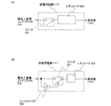
図25にアクティブタイプのRFIDの具体的な構成についてブロック図を示す。図25のアクティブタイプのRFID3100では、アンテナ回路3101によって受信された通信信号が信号処理回路3102における復調回路3105、アンプ3106に入力される。通常、通信信号は13.56MHz、915MHzなどのキャリアをASK変調、PSK変調などの処理をおこなって送られてくる。ここで図25においては、通信信号として13.56MHzを用いた例について示す。図25において、信号を処理するためには基準となるクロック信号が必要であり、ここでは13.56MHzのキャリアをクロックに用いている。アンプ3106は13.56MHzのキャリアを増幅し、クロックとして論理回路3107に供給する。またASK変調やPSK変調された通信信号は復調回路3105で復調される。復調後の信号も論理回路3107に送られ解析される。論理回路3107で解析された信号はメモリコントロール回路3108に送られ、それに基づき、メモリコントロール回路3108はメモリ回路3109を制御し、メモリ回路3109に記憶されたデータを取り出し論理回路3110に送られる。論理回路3110でエンコード処理されたのちアンプ3111で増幅され、その信号によって、変調回路3112はキャリアに変調をかける。ここで図25における電源は、信号処理回路3102の外に設けられる電池3103によって電源回路3104を介して供給している。そして電源回路3104はアンプ3106、復調回路3105、論理回路3107、メモリコントロール回路3108、メモリ回路3109、論理回路3110、アンプ3111、変調回路3112などに電力を供給する。このようにしてアクティブタイプのRFIDは動作する。
FIG. 25 is a block diagram showing a specific configuration of an active type RFID. In the
しかし、アクティブタイプのRFIDの場合、電池3103を内蔵しているため、電池の寿命が切れてしまうと使用できなくなる。従って、電池の寿命を把握する必要があり、また電池の寿命が切れてしまうと電池を交換する必要がある。さらに、RFIDタグの動作が停止しても、使用する状況によっては交換を即座に行えない場合も想定される。
However, in the case of an active type RFID, since the
またアクティブタイプのRFIDは、内蔵している電池の電気エネルギーが切れたとき、リーダからの問いかけに対して沈黙してしまう。この場合、電池切れにより沈黙しているのか、それとも電池以外の要因、例えば電波の状態が悪い、リーダに不具合が生じている等により沈黙しているのかが、使用者から一見して判別しにくいという問題があった。 In addition, when the electric energy of the built-in battery runs out, the active type RFID is silent with respect to the question from the reader. In this case, it is difficult for the user to determine at a glance whether the user is silenced due to the battery running out or whether it is silenced due to factors other than the battery, such as poor radio wave conditions or a problem with the reader. There was a problem.
次に、図26に、パッシブタイプのRFIDの具体的な構成についてブロック図を示す。図26のパッシブタイプのRFID3200では、アンテナ回路3201によって受信された通信信号が信号処理回路3202における復調回路3205、アンプ3206に入力される。通常、通信信号は13.56MHz、915MHzなどのキャリアをASK変調、PSK変調などの処理をおこなって送られてくる。図26においては、通信信号として13.56MHzを用いた例について示す。図26において、信号を処理するためには基準となるクロック信号が必要であり、ここでは13.56MHzのキャリアをクロックに用いている。アンプ3206は13.56MHzのキャリアを増幅し、クロックとして論理回路3207に供給する。またASK変調やPSK変調された通信信号は復調回路3205で復調される。復調後の信号も論理回路3207に送られ解析される。論理回路3207で解析された信号はメモリコントロール回路3208に送られ、それに基づき、メモリコントロール回路3208はメモリ回路3209を制御し、メモリ回路3209に記憶されたデータを取り出し論理回路3210に送られる。論理回路3210でエンコード処理されたのちアンプ3211で増幅され、その信号によって、変調回路3212はキャリアに変調をかける。一方、整流回路3203に入った通信信号は整流され、電源回路3204に入力される。電源回路3204はアンプ3206、復調回路3205、論理回路3207、メモリコントロール回路3208、メモリ回路3209、論理回路3210、アンプ3211、変調回路3212などに電力を供給する。このようにしてパッシブタイプのRFIDは動作する。
Next, FIG. 26 shows a block diagram of a specific configuration of a passive type RFID. In the
しかし、パッシブタイプのRFIDタグの場合、電力の送信元であるリーダライタからの電波または電磁波(搬送波)を受信できる距離でしか動作ができない、つまりリーダライタ近傍でしか動作することができないという問題がある。 However, in the case of a passive type RFID tag, there is a problem that it can operate only at a distance where radio waves or electromagnetic waves (carrier waves) from a reader / writer as a power transmission source can be received, that is, it can operate only near the reader / writer. is there.
上記の問題を解決する手段として、RFIDに電力を供給するための電源としてバッテリーを設ける方法がある。これにより、外部より電波または電磁波(搬送波)を受信していない場合でも、RFIDを利用することができる。特に、RFIDを物流システムなどに利用する場合には、一般的にバッテリーとして、小型で大容量の電気二重層コンデンサなどが搭載される。 As means for solving the above problem, there is a method of providing a battery as a power source for supplying power to the RFID. Thereby, even when radio waves or electromagnetic waves (carrier waves) are not received from the outside, RFID can be used. In particular, when the RFID is used in a distribution system or the like, a small and large-capacity electric double layer capacitor or the like is generally mounted as a battery.
このときに、RFIDが薄型で軽量であることが重要であるが、たとえ小さな電気二重層コンデンサを用いたとしても電気二重層コンデンサをRFIDに実装する場合、RFID自体の大きさや厚みが増してしまう。 At this time, it is important that the RFID is thin and light, but even when a small electric double layer capacitor is used, when the electric double layer capacitor is mounted on the RFID, the size and thickness of the RFID itself increases. .
また、電気二重層コンデンサをRFIDに実装するために、熱や光により硬化する樹脂中に導電性スペーサが分散された異方性導電膜を用いる場合、RFIDが高温になったときの熱膨張や低温になったときの熱収縮の割合が電気二重層コンデンサとRFIDで異なるため、接続部分の信頼性が低くなってしまう。 In addition, when an anisotropic conductive film in which conductive spacers are dispersed in a resin that is cured by heat or light is used to mount the electric double layer capacitor on the RFID, thermal expansion when the RFID becomes high temperature or Since the rate of heat shrinkage when the temperature becomes low differs between the electric double layer capacitor and the RFID, the reliability of the connection portion is lowered.
この問題を解決するために、電気二重層コンデンサをRFIDに一体に設ける方法が報告されており、CMOSにより形成された信号処理回路に隣接して、電気二重層コンデンサを一体に形成している(特許文献3)。
しかしながら、電気二重層コンデンサを信号処理回路に隣接して設ける場合、電気二重層コンデンサと信号処理回路を接続するための配線を引き回す必要がある。RFIDを物流システムなどに利用する場合は、球面を持っている対象物にRFIDを貼り付けることが多く、曲げることによりRFID自体に応力がかかる。以下、曲げることによりRFID自体にかかる応力を、曲げ応力という。特に、柔軟性を持ったフレキシブル基板で形成されたRFIDでは、電気二重層コンデンサと信号処理回路を接続するための配線にかかる曲げ応力は大きくなり、断線してしまうという課題があった。 However, when the electric double layer capacitor is provided adjacent to the signal processing circuit, it is necessary to route wiring for connecting the electric double layer capacitor and the signal processing circuit. When an RFID is used in a logistics system or the like, the RFID is often attached to an object having a spherical surface, and bending causes stress on the RFID itself. Hereinafter, the stress applied to the RFID itself by bending is referred to as bending stress. In particular, in an RFID formed of a flexible flexible substrate, there is a problem in that the bending stress applied to the wiring for connecting the electric double layer capacitor and the signal processing circuit is increased, resulting in disconnection.
上記問題を鑑み、本発明はRFIDなどの半導体装置において、基板上に設けられた充電用回路を有する信号処理回路上に、アンテナ回路および充電用の電気二重層コンデンサなどを一体的に形成した、曲げ応力に強い半導体装置を提供することを課題とする。 In view of the above problems, the present invention integrally forms an antenna circuit, an electric double layer capacitor for charging, etc. on a signal processing circuit having a charging circuit provided on a substrate in a semiconductor device such as RFID. It is an object to provide a semiconductor device that is resistant to bending stress.
上述の諸問題を解決するため、本発明は基板上に充電用回路を有する信号処理回路を設け、前記信号処理回路上にアンテナ回路および充電用の電気二重層コンデンサなどを一体的に形成することを特徴とする。また本発明は、充電用回路と電気二重層コンデンサを接続するための配線を短くし、曲げ応力による充電用の電気二重層コンデンサと充電用回路を有する信号処理回路との間の断線を防ぐために、基板上に充電用回路を有する信号処理回路を形成し、その上に充電用の電気二重層コンデンサを設けたことを特徴とする。これにより、信号処理回路に隣接して充電用の電気二重層コンデンサを設ける場合に比べ、より小型の半導体装置を作製することができる。以下、本発明の具体的な構成について示す。 In order to solve the above problems, the present invention provides a signal processing circuit having a charging circuit on a substrate, and an antenna circuit and a charging electric double layer capacitor are integrally formed on the signal processing circuit. It is characterized by. Further, the present invention shortens the wiring for connecting the charging circuit and the electric double layer capacitor, and prevents disconnection between the electric double layer capacitor for charging and the signal processing circuit having the charging circuit due to bending stress. A signal processing circuit having a charging circuit is formed on a substrate, and an electric double layer capacitor for charging is provided thereon. Thereby, a smaller semiconductor device can be manufactured as compared with the case where an electric double layer capacitor for charging is provided adjacent to the signal processing circuit. Hereinafter, a specific configuration of the present invention will be described.
本発明の半導体装置の一は、充電用回路を有する信号処理回路と、前記信号処理回路上に設けられたアンテナ回路および電気二重層コンデンサとを有し、前記アンテナ回路は、前記信号処理回路と電気的に接続されており前記電気二重層コンデンサは、前記充電用回路と電気的に接続されていることを特徴とする。 One of the semiconductor devices of the present invention includes a signal processing circuit having a charging circuit, an antenna circuit and an electric double layer capacitor provided on the signal processing circuit, and the antenna circuit includes the signal processing circuit and The electric double layer capacitor is electrically connected, and is electrically connected to the charging circuit.
また、別の本発明の半導体装置の一は、第1の基板上に設けられた充電用回路を有する信号処理回路と、前記信号処理回路上に設けられたアンテナ回路および電気二重層コンデンサと、前記アンテナ回路と電気二重層コンデンサ上に設けられた第2の基板を有し、前記アンテナ回路は、前記信号処理回路と電気的に接続されており、前記電気二重層コンデンサは、前記充電用回路と電気的に接続されていることを特徴とする。 Another semiconductor device of the present invention includes a signal processing circuit having a charging circuit provided on the first substrate, an antenna circuit and an electric double layer capacitor provided on the signal processing circuit, A second substrate provided on the antenna circuit and the electric double layer capacitor; the antenna circuit is electrically connected to the signal processing circuit; and the electric double layer capacitor is connected to the charging circuit. It is electrically connected to.
また、別の本発明の半導体装置の一は、充電用回路を有する信号処理回路と、前記信号処理回路上に設けられた絶縁膜と、前記絶縁膜上に設けられたアンテナ回路および電気二重層コンデンサとを有し、前記アンテナ回路は、前記絶縁膜を介して前記信号線処理回路と電気的に接続されており、前記電気二重層コンデンサは、前記絶縁膜を介して前記充電用回路と電気的に接続されていることを特徴とする。 Another semiconductor device of the present invention includes a signal processing circuit having a charging circuit, an insulating film provided on the signal processing circuit, an antenna circuit and an electric double layer provided on the insulating film. A capacitor, and the antenna circuit is electrically connected to the signal line processing circuit via the insulating film, and the electric double layer capacitor is electrically connected to the charging circuit via the insulating film. It is characterized by being connected.
また本発明における半導体装置は、上記の構成において、前記電気二重層コンデンサは、少なくとも第1の電極と、第2の電極と、前記第1の電極および前記第2の電極の間に位置する電解液層とを有し、前記第1の電極が前記充電用回路と電気的に接続されていることを特徴とする。 In the semiconductor device according to the present invention, in the above structure, the electric double layer capacitor includes at least a first electrode, a second electrode, an electrolysis located between the first electrode and the second electrode. And a liquid layer, wherein the first electrode is electrically connected to the charging circuit.
また本発明における半導体装置は、上記の構成において、前記第1の電極および前記第2の電極の少なくとも一方の前記電解液層側には、当該電極に接して活性炭、フラーレン、またはカーボンナノチューブからなる層が設けられていることを特徴とする。 In the semiconductor device according to the present invention, in the above structure, at least one of the first electrode and the second electrode is made of activated carbon, fullerene, or carbon nanotubes in contact with the electrode. A layer is provided.
また本発明における半導体装置は、上記の構成において、前記第1の電極もしくは前記第2の電極の少なくとも一方は、活性炭、フラーレン、またはカーボンナノチューブから形成されていることを特徴とする。 In the semiconductor device according to the present invention having the above structure, at least one of the first electrode and the second electrode is formed of activated carbon, fullerene, or a carbon nanotube.
また本発明における半導体装置は、上記の構成において、前記電気二重層コンデンサは、前記電解液層にセパレータを有してもよい。 In the semiconductor device according to the present invention, the electric double layer capacitor may have a separator in the electrolytic solution layer.
また本発明における半導体装置は、上記の構成において、前記電解液層は、架橋剤を有してもよい。 In the semiconductor device according to the present invention, the electrolyte layer may include a cross-linking agent in the above configuration.
また本発明における半導体装置は、上記の構成において、前記信号処理回路はトランジスタより構成されていることを特徴とする。 In the semiconductor device according to the present invention having the above structure, the signal processing circuit includes a transistor.
また本発明における半導体装置は、上記の構成において、前記基板は、柔軟性を持ったフレキシブル基板を用いたものであってもよい。 In the semiconductor device according to the present invention, the substrate may be a flexible substrate having flexibility.
また本発明における半導体装置は、上記の構成において、前記電気二重層コンデンサは、前記充電用回路と重なって位置することを特徴とする。 The semiconductor device according to the present invention is characterized in that, in the above structure, the electric double layer capacitor is positioned so as to overlap with the charging circuit.
本発明により、基板上に充電用の電気二重層コンデンサをアンテナ回路、信号処理回路などと一体的に形成した半導体装置を簡便に得ることができる。このように、充電用回路を有する信号処理回路上に電気二重層コンデンサを設けることで、充電用回路と電気二重層コンデンサを接続するための配線を短くすることができる。さらに、充電用回路と電気二重層コンデンサを接続するための配線が短いために、曲げ応力により断線しない充電用の電気二重層コンデンサを有する半導体装置を提供することができる。なお、本発明は、RFIDに限らず、薄型軽量な無線で充電するその他の電子機器にも適用することができる。 According to the present invention, a semiconductor device in which an electric double layer capacitor for charging is integrally formed with an antenna circuit, a signal processing circuit, or the like on a substrate can be easily obtained. Thus, by providing the electric double layer capacitor on the signal processing circuit having the charging circuit, the wiring for connecting the charging circuit and the electric double layer capacitor can be shortened. Furthermore, since the wiring for connecting the charging circuit and the electric double layer capacitor is short, a semiconductor device having a charging electric double layer capacitor that is not disconnected by bending stress can be provided. Note that the present invention can be applied not only to RFID but also to other electronic devices that are wirelessly charged with a thin and light weight.
以下、本発明の実施の形態について図面を参照しながら説明する。但し、本発明は多くの異なる態様で実施することが可能であり、本発明の趣旨及びその範囲から逸脱することなくその形態及び詳細を様々に変更し得ることは当業者であれば容易に理解される。従って本実施の形態の記載内容に限定して解釈されるものではない。なお、以下に説明する本発明の構成において、同じ物を指し示す符号は異なる図面間においても共通とする。 Hereinafter, embodiments of the present invention will be described with reference to the drawings. However, the present invention can be implemented in many different modes, and those skilled in the art can easily understand that the modes and details can be variously changed without departing from the spirit and scope of the present invention. Is done. Therefore, the present invention is not construed as being limited to the description of this embodiment mode. Note that in the structures of the present invention described below, the same reference numerals are used in different drawings.
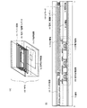
本発明のRFIDに用いる半導体装置について、図1(A)の斜視図、図1(B)の断面図および図2のブロック図を用いて説明する。なお、図1(B)の断面図は、図1(A)のXY間に相当する。 A semiconductor device used for the RFID of the present invention will be described with reference to a perspective view of FIG. 1A, a cross-sectional view of FIG. 1B, and a block diagram of FIG. Note that the cross-sectional view in FIG. 1B corresponds to the interval XY in FIG.
なお、本明細書でいう半導体装置とは、半導体特性を利用することで機能しうる装置全般を指すものとする。また、本明細書において、電極とは配線の一部であり、説明の便宜上、配線と電極と使い分けるが、配線という言葉には電極は常に含められているものとする。また、本明細書において、接続という言葉には電気的な接続は常に含められているものとする。 Note that a semiconductor device in this specification refers to all devices that can function by utilizing semiconductor characteristics. In this specification, an electrode is a part of a wiring, and for convenience of explanation, the wiring and the electrode are used separately. However, the word “wiring” always includes an electrode. In this specification, the term “connection” always includes electrical connection.
図1(A)、(B)のRFID100は、アンテナ回路101、充電用回路116を有する信号処理回路102及びセパレータ120を有する電気二重層コンデンサ104によって構成されている。図2に示すように、信号処理回路102は、整流回路105、レギュレータからなる充電用回路116、放電用回路117、復調回路108、アンプ109、論理回路110、メモリコントロール回路111、メモリ回路112、論理回路113、アンプ114、変調回路115によって構成される。
1A and 1B includes an antenna circuit 101, a signal processing circuit 102 having a charging circuit 116, and an electric double layer capacitor 104 having a separator 120. As shown in FIG. 2, the signal processing circuit 102 includes a
なおアンテナ回路101におけるアンテナの形状については、特に限定されない。例えば図3(A)のように基板10上の信号処理回路102の周りに一面のアンテナ303を配した構造を取っても良い。また、図3(B)のように基板10上の信号処理回路102に接続されたコイル状のアンテナ303でも良い。また、図3(C)のように基板10上の信号処理回路102に対して、高周波数の電磁波を受信するためのアンテナ303の形状をとってもよい。また、図3(D)のように基板10上の信号処理回路102に対して、180度無指向性(どの方向からでも同じく受信可能)なアンテナ303での形状をとってもよい。また、図3(E)のように、基板10上の信号処理回路102に対して、棒状に長く伸ばしたアンテナ303の形状をとってもよい。また、アンテナに必要な長さは受信に用いる周波数によって長さが異なる。例えば周波数が2.45GHzの場合は、半波長ダイポールアンテナを設けるなら約60mm(1/2波長)、モノポールアンテナを設けるなら約30mm(1/4波長)とすれば良い。本実施の形態におけるアンテナ回路101は、図4(A)に示すようにアンテナ141、共振容量142によって構成されるものとして説明し、アンテナ141及び共振容量142を併せてアンテナ回路101ということにする。 Note that the shape of the antenna in the antenna circuit 101 is not particularly limited. For example, as shown in FIG. 3A, a structure in which one antenna 303 is arranged around the signal processing circuit 102 on the substrate 10 may be employed. Alternatively, a coiled antenna 303 connected to the signal processing circuit 102 on the substrate 10 may be used as shown in FIG. Further, as shown in FIG. 3C, the shape of an antenna 303 for receiving high-frequency electromagnetic waves may be taken for the signal processing circuit 102 on the substrate 10. Further, as shown in FIG. 3D, the signal processing circuit 102 on the substrate 10 may have a shape with an antenna 303 that is 180 degrees omnidirectional (same reception is possible from any direction). Further, as shown in FIG. 3E, the antenna 303 may be formed in a bar shape with respect to the signal processing circuit 102 on the substrate 10. The length required for the antenna differs depending on the frequency used for reception. For example, when the frequency is 2.45 GHz, it may be about 60 mm (1/2 wavelength) if a half-wave dipole antenna is provided, and about 30 mm (1/4 wavelength) if a monopole antenna is provided. The antenna circuit 101 in this embodiment is described as including an antenna 141 and a resonant capacitor 142 as illustrated in FIG. 4A, and the antenna 141 and the resonant capacitor 142 are collectively referred to as the antenna circuit 101. .
また、整流回路105は、アンテナ回路101が受信する電磁波により誘導される交流信号を直流信号に変換する回路であればよい。例えば、図4(B)に示すように、整流特性を有するダイオード143、平滑容量144によって整流回路105を構成すればよい。
The
充電用回路116は、整流回路105より入力された電気信号の電圧レベルを制御して電気二重層コンデンサ104に出力する回路であればよい。例えば、図5(A)に示すように、電圧を制御する回路であるレギュレータ145と整流特性を有するダイオード146で構成することができる。ダイオード146は、電気二重層コンデンサ104に充電された電力の漏洩を防止するものである。そのため、図5(B)に示すように、ダイオード146をスイッチ147に置き換えた構成としてもよい。スイッチ147を設ける場合、電気二重層コンデンサ104の充電が行われている状態ではオンにし、充電が行われていない状態ではオフとすることにより電気二重層コンデンサ104に充電された電力の漏洩を防止できる。
The charging circuit 116 may be any circuit that controls the voltage level of the electric signal input from the
図2に示すように、充電用回路116により電圧レベルが制御された電源電圧は、電気二重層コンデンサ104に入力され、電気二重層コンデンサ104に充電される。電気二重層コンデンサ104に充電された電力は、放電用回路117を介して負荷部118へ供給、つまり電気二重層コンデンサ104の放電が行われる。 As shown in FIG. 2, the power supply voltage whose voltage level is controlled by the charging circuit 116 is input to the electric double layer capacitor 104 and charged in the electric double layer capacitor 104. The electric power charged in the electric double layer capacitor 104 is supplied to the load unit 118 through the discharge circuit 117, that is, the electric double layer capacitor 104 is discharged.
放電用回路117は、電気二重層コンデンサ104より出力された電圧レベルを制御して、電気二重層コンデンサ104の放電を制御する回路であればよい。例えば、図6(A)に示すように、スイッチ501と、電圧制御する回路であるレギュレータ502で構成することができる。スイッチ501のオン又はオフを制御することにより、電気二重層コンデンサ104から負荷部118への電力の供給の有無を制御することができる。
The discharge circuit 117 may be any circuit that controls the voltage level output from the electric double layer capacitor 104 and controls the discharge of the electric double layer capacitor 104. For example, as shown in FIG. 6A, a
また、電気二重層コンデンサ104の電圧値に応じてスイッチ501のオン又はオフを制御する構成としてもよい。例えば、図6(A)に示す構成にシュミットトリガー503を組み合わせた構成とすることができる(図6(B)参照)。シュミットトリガー503は、スイッチング素子に履歴現象(ヒステリシス性)を持たせることができる。具体的には、入力電圧に対して上限値と下限値との2つのスレッショルドレベルを持ち、これらの値より入力が高くなるか、あるいは低くなるかによりオン、オフを制御することができる。例えば、電気二重層コンデンサ104の電圧値が5V以上の場合にスイッチ501がオンし、3V以下でオフすることができる。つまり、電気二重層コンデンサ104に一定の電力が充電される場合に限って負荷部118に電力を供給する構成とすることができる。
Alternatively, the
次に、RFID100の基板上にアンテナ回路101、信号処理回路102と一体形成された充電用の電気二重層コンデンサ104について説明する。
Next, the electric double layer capacitor 104 for charging formed integrally with the antenna circuit 101 and the signal processing circuit 102 on the substrate of the
本実施の形態では、図1(B)のように基板10上に信号処理回路102を有する充電用回路116が形成されており、その上に電気二重層コンデンサ104が形成されている。電気二重層コンデンサ104の第1の電極11は、充電用回路116のトランジスタに電気的に接続されている。また、第1の電極11上には電解液層12が設けられていて、その上に第2の電極13が設けられている。つまり、少なくとも第1の電極11、電解液層12、第2の電極13で電気二重層コンデンサ104を形成している。 In this embodiment, a charging circuit 116 having a signal processing circuit 102 is formed over a substrate 10 as shown in FIG. 1B, and an electric double layer capacitor 104 is formed thereon. The first electrode 11 of the electric double layer capacitor 104 is electrically connected to the transistor of the charging circuit 116. An electrolyte layer 12 is provided on the first electrode 11, and a second electrode 13 is provided thereon. That is, the electric double layer capacitor 104 is formed by at least the first electrode 11, the electrolyte solution layer 12, and the second electrode 13.
電気二重層コンデンサ104は、充電時は電極表面に電解液中のイオンを物理的に吸着し、放電時には電極表面のイオンを脱着させる。このように充放電に伴って電解液中のイオンは、電極界面に吸脱着する。そのため、電気化学反応を伴う二次電池と異なり充放電を繰り返しても、物質変化がない。したがって、二次電池に比べ、性能劣化が極めて少なく、また使用可能な温度範囲も広い。また、電気二重層コンデンサ104は、電極界面に電解液中のイオンが吸脱着することで充放電を行うため、放熱しない。そのため、充電用回路116を含む信号処理回路102上に電気二重層コンデンサ104を形成しても、充電用回路116のトランジスタや信号処理回路102のトランジスタへの熱による影響も抑制できる。 The electric double layer capacitor 104 physically adsorbs ions in the electrolytic solution on the electrode surface during charging, and desorbs ions on the electrode surface during discharging. As described above, ions in the electrolytic solution are adsorbed and desorbed on the electrode interface along with charge and discharge. Therefore, unlike a secondary battery with an electrochemical reaction, there is no material change even when charging and discharging are repeated. Therefore, compared with the secondary battery, the performance deterioration is extremely small and the usable temperature range is wide. In addition, the electric double layer capacitor 104 does not dissipate heat because charge and discharge are performed by ions adsorbed and desorbed on the electrode interface. Therefore, even if the electric double layer capacitor 104 is formed on the signal processing circuit 102 including the charging circuit 116, the influence of heat on the transistor of the charging circuit 116 and the transistor of the signal processing circuit 102 can be suppressed.
なお、第1の電極11と第2の電極13は、化学的気相成長法(CVD法)やスパッタリング法等により、アルミニウム(Al)、タングステン(W)、チタン(Ti)、タンタル(Ta)、モリブデン(Mo)、ニッケル(Ni)、白金(Pt)、銅(Cu)、金(Au)、銀(Ag)、マンガン(Mn)、ネオジム(Nd)、炭素(C)、シリコン(Si)から選択された元素、又はこれらの元素を主成分とする合金材料もしくは化合物材料で、単層又は積層の導電膜から形成することができる。 Note that the first electrode 11 and the second electrode 13 are formed of aluminum (Al), tungsten (W), titanium (Ti), tantalum (Ta) by chemical vapor deposition (CVD), sputtering, or the like. , Molybdenum (Mo), nickel (Ni), platinum (Pt), copper (Cu), gold (Au), silver (Ag), manganese (Mn), neodymium (Nd), carbon (C), silicon (Si) Or an alloy material or a compound material containing these elements as a main component, and can be formed from a single layer or a stacked conductive film.
また、電気二重層コンデンサ104の電解液層12は、溶媒と電解質からなる電解液で構成される。電解質としては、溶媒中における解離度が高いこと、解離したイオンの移動度が高いこと、イオン種が酸化還元反応による分解などの副反応を受けにくいなどの性質を有するものを用いることが好ましい。たとえば、電解質として硫酸や水酸化カリウムなどを用いることができる。また溶媒としては、高い誘電率を持つこと、溶媒粘度が低いこと、酸化電位と還元電位の電位差が大きいなどの性質を有するものを用いることが好ましい。なお、溶媒は水溶液系と非水溶液系に分けることができる。水溶液系の溶媒の代表例は、水である。水溶液系は非水溶液系に比べ、電解液のコスト、安全性、充電の急速性の面で有利である。一方、非水溶液系の溶媒の代表例は、メタノール、アセトニトリル、プロピレンカーボネートなどである。非水溶液系は水溶液系に比べ、作動温度範囲が広いという面で有利である。また、電解液として、イオン性液体を用いても良い。ここでは、イオン性液体も電解液に含まれるものとする。また、電気二重層コンデンサの電解液層12としては、液漏れによる劣化故障を起こさず、イオン伝導度の低下が少ないゲル状固体電解液を用いることもできる。このゲル状固体電解液は、電解質と水に可溶であり酸性物質または塩基性物質に対してゲル状を呈する高分子化合物を有する。また、電気二重層コンデンサ104の電解液層12に、架橋剤などを混ぜておき加熱や紫外線照射をすることで、ゲル化することも可能である。このように、電気二重層コンデンサ104の電解液層12をゲル化することで、電解液が漏れることを容易に防ぐことができる。 The electrolytic solution layer 12 of the electric double layer capacitor 104 is composed of an electrolytic solution composed of a solvent and an electrolyte. As the electrolyte, it is preferable to use an electrolyte having properties such as a high degree of dissociation in a solvent, a high mobility of dissociated ions, and an ionic species that is less susceptible to side reactions such as decomposition due to a redox reaction. For example, sulfuric acid or potassium hydroxide can be used as the electrolyte. Further, it is preferable to use a solvent having properties such as having a high dielectric constant, a low solvent viscosity, and a large potential difference between the oxidation potential and the reduction potential. The solvent can be divided into an aqueous solution system and a non-aqueous solution system. A typical example of the aqueous solvent is water. The aqueous solution system is more advantageous than the non-aqueous solution system in terms of the cost of the electrolyte, safety, and rapid charging. On the other hand, typical examples of non-aqueous solvents are methanol, acetonitrile, propylene carbonate, and the like. Non-aqueous systems are advantageous in that they have a wider operating temperature range than aqueous systems. An ionic liquid may be used as the electrolytic solution. Here, an ionic liquid is also included in the electrolytic solution. Further, as the electrolytic solution layer 12 of the electric double layer capacitor, a gel-like solid electrolytic solution that does not cause deterioration failure due to liquid leakage and has a small decrease in ionic conductivity can also be used. This gel-like solid electrolytic solution has a polymer compound that is soluble in an electrolyte and water and exhibits a gel state with respect to an acidic substance or a basic substance. Moreover, it can be gelled by mixing the electrolyte layer 12 of the electric double layer capacitor 104 with a crosslinking agent or the like and heating or irradiating with ultraviolet rays. Thus, by making the electrolytic solution layer 12 of the electric double layer capacitor 104 into a gel, it is possible to easily prevent the electrolytic solution from leaking.
なお、電気二重層コンデンサ104による容量は、第1の電極11および第2の電極13と電解液層12との界面の面積に影響される。第1の電極11および第2の電極13の比表面積が大きいほど、電気二重層コンデンサ104による容量も大きくなる。そのため、第1の電極11および第2の電極13の上にこれら電極の比表面積を増大させる機能を有する層を設けても良い。当該層は、活性炭やナノレベルの炭素、例えばフラーレンや垂直配向したカーボンナノチューブ、や金属酸化物や導電性高分子等で形成することができる。例えば、電極上にスピンコート法などで金属触媒として機能する鉄、コバルト、ニッケル、銅などを塗布し、その後アーク放電法、レーザー蒸着法、レーザーアブレーション法、化学的気相成長法(CVD法)などにより、カーボンナノチューブなどのナノレベルの炭素を成長させることで、低抵抗であり、比表面積の大きい電極として機能させることができる。また、第1の電極11および第2の電極13を上述の材料を用いずに、上述の比表面積を増大させる機能を有する層で代用しても良い。 The capacity of the electric double layer capacitor 104 is affected by the area of the interface between the first electrode 11 and the second electrode 13 and the electrolyte layer 12. The larger the specific surface area of the first electrode 11 and the second electrode 13, the larger the capacitance by the electric double layer capacitor 104. Therefore, a layer having a function of increasing the specific surface area of these electrodes may be provided on the first electrode 11 and the second electrode 13. The layer can be formed of activated carbon or nano-level carbon such as fullerene or vertically aligned carbon nanotubes, a metal oxide, a conductive polymer, or the like. For example, iron, cobalt, nickel, copper, etc. that function as a metal catalyst are applied on the electrodes by spin coating, etc., and then arc discharge, laser deposition, laser ablation, chemical vapor deposition (CVD) By growing nano-level carbon such as carbon nanotubes, it is possible to function as an electrode having a low resistance and a large specific surface area. Alternatively, the first electrode 11 and the second electrode 13 may be replaced with a layer having a function of increasing the specific surface area described above without using the above-described material.
セパレータ120は、電気二重層コンデンサ104の第1の電極11と第2の電極13の短絡を防ぐ役割を持つ。そのため、電解液中のイオンが通過することができる孔を有する多孔質の構造からなる。柔軟性があり、機械的強度があり、耐久性も高いポリエチレンまたはポリプロピレンなどの多孔性ポリマーフィルムなどを用いることができる。 The separator 120 has a role of preventing a short circuit between the first electrode 11 and the second electrode 13 of the electric double layer capacitor 104. Therefore, it consists of a porous structure having pores through which ions in the electrolyte can pass. A porous polymer film such as polyethylene or polypropylene having flexibility, mechanical strength, and high durability can be used.
以上のように、充電用回路116上に電気二重層コンデンサ104を設けることで、電気二重層コンデンサをRFIDに実装する場合に比べて、薄型で軽量なRFIDを作製することができる。また、充電用回路116を有する信号処理回路102上に電気二重層コンデンサ104を設けることで、充電用回路116と電気二重層コンデンサ104を接続するための配線を短くすることができるため、電気二重層コンデンサ104と充電用回路116を有する信号処理回路102との間で生じる断線を防ぐことができる。 As described above, by providing the electric double layer capacitor 104 on the charging circuit 116, a thinner and lighter RFID can be manufactured as compared with the case where the electric double layer capacitor is mounted on the RFID. Further, by providing the electric double layer capacitor 104 over the signal processing circuit 102 having the charging circuit 116, the wiring for connecting the charging circuit 116 and the electric double layer capacitor 104 can be shortened. Disconnection between the multilayer capacitor 104 and the signal processing circuit 102 having the charging circuit 116 can be prevented.
なお、本実施の形態は、本明細書中の実施例の記載と適宜組み合わせても良い。 Note that this embodiment mode may be appropriately combined with the description of the examples in this specification.
本実施例では、上記実施の形態で示したRFIDの作製方法について説明する。 In this example, a method for manufacturing the RFID described in the above embodiment is described.
まず、図7(A)に示すように、基板701の一表面に下地膜として機能する絶縁膜704と半導体膜705(例えば、非晶質珪素を含む膜)を積層して形成する。なお、絶縁膜704および半導体膜705は、連続して形成することができる。
First, as illustrated in FIG. 7A, an insulating
なお、基板701は、ガラス基板、石英基板、金属基板(例えばステンレス基板など)、セラミック基板、Si基板等の半導体基板から選択されるものである。他にもプラスチック基板として、ポリエチレンテレフタレート(PET)、ポリエチレンナフタレート(PEN)、ポリエーテルサルフォン(PES)、アクリルなどの基板を選択することもできる。
The
また、絶縁膜704は、化学的気相成長法(CVD法)やスパッタリング法等を用いて、酸化シリコン、窒化シリコン、酸化窒化シリコン(SiOxNy)(x>y>0)、窒化酸化シリコン(SiNxOy)(x>y>0)等の絶縁材料を用いて形成する。例えば、絶縁膜704を2層構造とする場合、第1層目の絶縁膜として窒化酸化シリコン膜を形成し、第2層目の絶縁膜として酸化窒化シリコン膜を形成するとよい。また、第1層目の絶縁膜として窒化シリコン膜を形成し、第2層目の絶縁膜として酸化シリコン膜を形成してもよい。絶縁膜704は、基板701から半導体膜705への不純物元素が混入するのを防ぐブロッキング層として機能し、このように、ブロッキング層として機能する絶縁膜704を形成することによって、基板701からNaなどのアルカリ金属やアルカリ土類金属が、半導体膜705に悪影響を与えることを防ぐことができる。なお、基板701として石英を用いるような場合には絶縁膜704を省略してもよい。
The insulating
また、半導体膜705は、スパッタリング法、LPCVD法、プラズマCVD法等により、25〜200nm(好ましくは30〜150nm)の厚さで形成する。
The
次に、図7(B)に示すように、半導体膜705にレーザー光を照射して結晶化を行う。なお、レーザー光の照射と、RTA又はファーネスアニール炉を用いる熱結晶化法、結晶化を助長する金属元素を用いる熱結晶化法とを組み合わせた方法等により半導体膜705の結晶化を行ってもよい。その後、図7(B)に示すように、得られた結晶質半導体膜を所望の形状にエッチングして、結晶化した結晶質半導体膜705a〜705cを形成し、当該結晶質半導体膜705a〜705cを覆うようにゲート絶縁膜706を形成する。
Next, as shown in FIG. 7B, the
なお、ゲート絶縁膜706は、化学的気相成長法(CVD法)やスパッタリング法等を用いて、酸化シリコン、窒化シリコン、酸化窒化シリコン(SiOxNy)(x>y>0)、窒化酸化シリコン(SiNxOy)(x>y>0)等の絶縁材料を用いて形成する。例えば、ゲート絶縁膜706を2層構造とする場合、第1層目の絶縁膜として酸化窒化シリコン膜を形成し、第2層目の絶縁膜として窒化酸化シリコン膜を形成するとよい。また、第1層目の絶縁膜として酸化シリコン膜を形成し、第2層目の絶縁膜として窒化シリコン膜を形成してもよい。
Note that the
結晶質半導体膜705a〜705cの作製工程の一例を以下に簡単に説明すると、まず、プラズマCVD法を用いて、膜厚50〜60nmの非晶質半導体膜を形成する。次に、結晶化を助長する金属元素であるニッケルを含む溶液を非晶質半導体膜上に保持させた後、非晶質半導体膜に脱水素化の処理(500℃、1時間)と、熱結晶化の処理(550℃、4時間)を行って結晶質半導体膜を形成する。その後、レーザー光を照射し、フォトリソグラフィ法を用いることよって結晶質半導体膜705a〜705cを形成する。なお、結晶化を助長する金属元素を用いる熱結晶化を行わずに、レーザー光の照射だけで非晶質半導体膜の結晶化を行ってもよい。
An example of a manufacturing process of the
なお、結晶化に用いるレーザー発振器としては、連続発振型のレーザー(CWレーザー)やパルス発振型のレーザー(パルスレーザー)を用いることができる。ここで用いることができるレーザービームは、Arレーザー、Krレーザー、エキシマレーザーなどの気体レーザー、単結晶のYAG、YVO4、フォルステライト(Mg2SiO4)、YAlO3、GdVO4、もしくは多結晶(セラミック)のYAG、Y2O3、YVO4、YAlO3、GdVO4に、ドーパントとしてNd、Yb、Cr、Ti、Ho、Er、Tm、Taのうち1種または複数種添加されているものを媒質とするレーザー、ガラスレーザー、ルビーレーザー、アレキサンドライトレーザー、Ti:サファイアレーザー、銅蒸気レーザーまたは金蒸気レーザーのうち一種または複数種から発振されるものを用いることができる。このようなレーザービームの基本波、及びこれらの基本波の第2高調波から第4高調波のレーザービームを照射することで、大粒径の結晶を得ることができる。例えば、Nd:YVO4レーザー(基本波1064nm)の第2高調波(532nm)や第3高調波(355nm)を用いることができる。このときレーザーのパワー密度は0.01〜100MW/cm2程度(好ましくは0.1〜10MW/cm2)が必要である。そして、走査速度を10〜2000cm/sec程度として照射する。なお、単結晶のYAG、YVO4、フォルステライト(Mg2SiO4)、YAlO3、GdVO4、もしくは多結晶(セラミック)のYAG、Y2O3、YVO4、YAlO3、GdVO4に、ドーパントとしてNd、Yb、Cr、Ti、Ho、Er、Tm、Taのうち1種または複数種添加されているものを媒質とするレーザー、Arイオンレーザー、またはTi:サファイアレーザーは、連続発振をさせることが可能であり、Qスイッチ動作やモード同期などを行うことによって10MHz以上の発振周波数でパルス発振をさせることも可能である。10MHz以上の発振周波数でレーザービームを発振させると、半導体膜がレーザーによって溶融してから固化するまでの間に、次のパルスが半導体膜に照射される。従って、発振周波数が低いパルスレーザーを用いる場合と異なり、半導体膜中において固液界面を連続的に移動させることができるため、走査方向に向かって連続的に成長した結晶粒を得ることができる。 Note that as a laser oscillator used for crystallization, a continuous wave laser (CW laser) or a pulsed laser (pulse laser) can be used. Laser beams that can be used here are gas lasers such as Ar laser, Kr laser, and excimer laser, single crystal YAG, YVO 4 , forsterite (Mg 2 SiO 4 ), YAlO 3 , GdVO 4 , or polycrystalline ( Ceramic) YAG, Y 2 O 3 , YVO 4 , YAlO 3 , GdVO 4 with one or more of Nd, Yb, Cr, Ti, Ho, Er, Tm, Ta added as dopants Lasers oscillated from one or more of laser, glass laser, ruby laser, alexandrite laser, Ti: sapphire laser, copper vapor laser or gold vapor laser as a medium can be used. By irradiating the fundamental wave of such a laser beam and the second to fourth harmonics of these fundamental waves, a crystal having a large grain size can be obtained. For example, the second harmonic (532 nm) or the third harmonic (355 nm) of an Nd: YVO 4 laser (fundamental wave 1064 nm) can be used. In this case, a laser power density is about 0.01 to 100 MW / cm 2 (preferably 0.1 to 10 MW / cm 2) is required. Then, irradiation is performed at a scanning speed of about 10 to 2000 cm / sec. Note that single crystal YAG, YVO 4 , forsterite (Mg 2 SiO 4 ), YAlO 3 , GdVO 4 , or polycrystalline (ceramic) YAG, Y 2 O 3 , YVO 4 , YAlO 3 , GdVO 4 , dopants Nd, Yb, Cr, Ti, Ho, Er, Tm, Ta as a medium, a laser, Ar ion laser, or Ti: sapphire laser with one or more added as a medium should be continuously oscillated It is also possible to perform pulse oscillation at an oscillation frequency of 10 MHz or more by performing Q switch operation, mode synchronization, or the like. When a laser beam is oscillated at an oscillation frequency of 10 MHz or higher, the semiconductor film is irradiated with the next pulse during the period from when the semiconductor film is melted by the laser to solidification. Therefore, unlike the case of using a pulse laser having a low oscillation frequency, the solid-liquid interface can be continuously moved in the semiconductor film, so that crystal grains continuously grown in the scanning direction can be obtained.
また、ゲート絶縁膜706は、半導体膜705a〜705cに対し高密度プラズマ処理を行い、表面を酸化又は窒化することで形成しても良い。例えば、He、Ar、Kr、Xeなどの希ガスと、酸素、酸化窒素(NO2)、アンモニア、窒素、水素などの混合ガスを導入したプラズマ処理で形成する。この場合のプラズマの励起は、マイクロ波の導入により行うと、低電子温度で高密度のプラズマを生成することができる。この高密度プラズマで生成された酸素ラジカル(OHラジカルを含む場合もある)や窒素ラジカル(NHラジカルを含む場合もある)によって、半導体膜の表面を酸化又は窒化することができる。
Alternatively, the
このような高密度プラズマを用いた処理により、1〜20nm、代表的には5〜10nmの絶縁膜が半導体膜に形成される。この場合の反応は、固相反応であるため、当該絶縁膜と半導体膜との界面準位密度はきわめて低くすることができる。このような、高密度プラズマ処理は、半導体膜(結晶性シリコン、あるいは多結晶シリコン)の表面を直接酸化(もしくは窒化)するため、形成される絶縁膜の厚さは理想的には、ばらつきをきわめて小さくすることができる。加えて、結晶性シリコンの結晶粒界でも酸化が強くされることがないため、非常に好ましい状態となる。すなわち、ここで示す高密度プラズマ処理で半導体膜の表面を固相酸化することにより、結晶粒界において異常に酸化反応をさせることなく、均一性が良く、界面準位密度が低い絶縁膜を形成することができる。 By such treatment using high-density plasma, an insulating film with a thickness of 1 to 20 nm, typically 5 to 10 nm, is formed over the semiconductor film. Since the reaction in this case is a solid-phase reaction, the interface state density between the insulating film and the semiconductor film can be extremely low. Such high-density plasma treatment directly oxidizes (or nitrides) the surface of the semiconductor film (crystalline silicon or polycrystalline silicon), so that the thickness of the formed insulating film ideally varies. Can be very small. In addition, since oxidation is not strengthened even at the crystal grain boundaries of crystalline silicon, a very favorable state is obtained. That is, the surface of the semiconductor film is solid-phase oxidized by the high-density plasma treatment shown here, thereby forming an insulating film with good uniformity and low interface state density without causing an abnormal oxidation reaction at the grain boundaries. can do.
なお、ゲート絶縁膜706は、高密度プラズマ処理によって形成される絶縁膜のみを用いても良いし、それにプラズマや熱反応を利用したCVD法で酸化シリコン、酸窒化シリコン、窒化シリコンなどの絶縁膜を堆積し、積層させても良い。いずれにしても、高密度プラズマで形成した絶縁膜をゲート絶縁膜の一部又は全部に含んで形成されるトランジスタは、特性のばらつきを小さくすることができる。
Note that as the
また、半導体膜に対し、連続発振レーザービームもしくは10MHz以上の周波数で発振するレーザービームを照射しながら一方向に走査して結晶化させて得られた半導体膜705a〜705cは、そのビームの走査方向に結晶が成長する特性がある。その走査方向をチャネル長方向(チャネル形成領域が形成されたときにキャリアが流れる方向)に合わせてトランジスタを配置し、上記ゲート絶縁層を組み合わせることで、特性ばらつきが小さく、しかも電界効果移動度が高い薄膜トランジスタ(TFT:Thin Film Transistor)を得ることができる。
Further, the
次に、ゲート絶縁膜706上に、第1の導電膜と第2の導電膜とを積層して形成する。ここでは、第1の導電膜は、化学的気相成長法(CVD法)やスパッタリング法等により、20〜100nmの厚さで形成する。第2の導電膜は、100〜400nmの厚さで形成する。第1の導電膜と第2の導電膜は、タンタル(Ta)、タングステン(W)、チタン(Ti)、モリブデン(Mo)、アルミニウム(Al)、銅(Cu)、クロム(Cr)、ニオブ(Nb)等から選択された元素又はこれらの元素を主成分とする合金材料もしくは化合物材料で形成する。または、リン等の不純物元素をドーピングした多結晶珪素に代表される半導体材料により形成する。第1の導電膜と第2の導電膜の組み合わせの例を挙げると、窒化タンタル膜とタングステン膜、窒化タングステン膜とタングステン膜、窒化モリブデン膜とモリブデン膜等が挙げられる。タングステンや窒化タンタルは、耐熱性が高いため、第1の導電膜と第2の導電膜を形成した後に、熱活性化を目的とした加熱処理を行うことができる。また、2層構造ではなく、3層構造の場合は、モリブデン膜とアルミニウム膜とモリブデン膜の積層構造を採用するとよい。
Next, a first conductive film and a second conductive film are stacked over the
次に、フォトリソグラフィ法を用いてレジストからなるマスクを形成し、ゲート電極とゲート線を形成するためのエッチング処理を行って、半導体膜705a〜705cの上方にゲート電極707を形成する。ここでは、ゲート電極707として、第1の導電膜707aと第2の導電膜707bの積層構造で設けた例を示している。
Next, a mask made of a resist is formed using a photolithography method, and an etching process for forming a gate electrode and a gate line is performed, so that a
次に、図7(C)に示すように、ゲート電極707をマスクとして半導体膜705a〜705cに、イオンドープ法またはイオン注入法により、n型を付与する不純物元素を低濃度に添加し、その後、フォトリソグラフィ法によりレジストからなるマスクを選択的に形成して、半導体膜705bにp型を付与する不純物元素を高濃度に添加する。n型を示す不純物元素としては、リン(P)やヒ素(As)等を用いることができる。p型を示す不純物元素としては、ボロン(B)やアルミニウム(Al)やガリウム(Ga)等を用いることができる。ここでは、n型を付与する不純物元素としてリン(P)を用い、1×10¹⁵〜1×10¹⁷/cm3の濃度で含まれるように半導体膜705a〜705cに選択的に導入し、n型を示す不純物領域708を形成する。また、p型を付与する不純物元素としてボロン(B)を用い、1×1017〜1×1020/cm3の濃度で含まれるように選択的に半導体膜705bに導入し、p型を示す不純物領域709を形成する。
Next, as illustrated in FIG. 7C, an impurity element imparting n-type conductivity is added to the
続いて、ゲート絶縁膜706とゲート電極707を覆うように、絶縁膜を形成する。絶縁膜は、プラズマCVD法やスパッタリング法等により、珪素、珪素の酸化物又は珪素の窒化物等の無機材料を含む膜や、有機樹脂などの有機材料を含む膜を、単層又は積層して形成する。次に、絶縁膜を、垂直方向を主体とした異方性エッチングにより選択的にエッチングして、ゲート電極707の側面に接する絶縁膜710(サイドウォールともよばれる)を形成する。絶縁膜710は、LDD(Lightly Doped Drain)領域を形成する際のドーピング用のマスクとして用いる。
Subsequently, an insulating film is formed so as to cover the
続いて、フォトリソグラフィ法により形成したレジストからなるマスクと、ゲート電極707および絶縁膜710をマスクとして用いて、半導体膜705a、705cにn型を付与する不純物元素を高濃度に添加して、n型を示す不純物領域711を形成する。ここでは、n型を付与する不純物元素としてリン(P)を用い、1×10¹⁷〜1×10²⁰/cm3の濃度で含まれるように半導体膜705a、705cに選択的に導入し、不純物領域708より高濃度のn型を示す不純物領域711を形成する。
Subsequently, an impurity element imparting n-type conductivity is added to the
以上の工程により、図7(D)に示すように、nチャネル型薄膜トランジスタ700a、700cとpチャネル型薄膜トランジスタ700bが形成される。
Through the above steps, n-channel
なお、nチャネル型薄膜トランジスタ700aは、ゲート電極707と重なる半導体膜705aの領域にチャネル形成領域が形成され、ゲート電極707及び絶縁膜710と重ならない領域にソース領域又はドレイン領域を形成する不純物領域711が形成され、絶縁膜710と重なる領域であってチャネル形成領域と不純物領域711の間に低濃度不純物領域(LDD領域712)が形成されている。また、nチャネル型薄膜トランジスタ700cも同様にチャネル形成領域、低濃度不純物領域及び不純物領域711が形成されている。
Note that in the n-channel
また、pチャネル型薄膜トランジスタ700bは、ゲート電極707と重なる半導体膜705bの領域にチャネル形成領域が形成され、ゲート電極707と重ならない領域にソース領域又はドレイン領域を形成する不純物領域709が形成されている。なお、ここでは、pチャネル型薄膜トランジスタ700bには、LDD領域を設けていないが、pチャネル型薄膜トランジスタにLDD領域を設けてもよいし、nチャネル型薄膜トランジスタにLDD領域を設けない構成としてもよい。
In the p-channel
次に、図8(A)に示すように、半導体膜705a〜705c、ゲート電極707等を覆うように、絶縁膜を単層または積層して形成し、当該絶縁膜上に薄膜トランジスタ700a〜700cのソース領域又はドレイン領域を形成する不純物領域709、711と電気的に接続する導電膜713を形成する。絶縁膜は、化学的気相成長法(CVD法)、スパッタリング法、SOG法、液滴吐出法、スクリーン印刷法等により、珪素の酸化物や珪素の窒化物等の無機材料、ポリイミド、ポリアミド、ベンゾシクロブテン、アクリル、エポキシ等の有機材料やシロキサン材料等により、単層または積層で形成する。ここでは、当該絶縁膜を2層で設け、1層目の絶縁膜712aとして窒化酸化珪素膜で形成し、2層目の絶縁膜712bとして酸化窒化珪素膜で形成する。また、導電膜713は、半導体膜705a〜705cのソース電極又はドレイン電極を形成する。
Next, as illustrated in FIG. 8A, an insulating film is formed as a single layer or a stacked layer so as to cover the
なお、絶縁膜712a、712bを形成する前、または絶縁膜712a、712bのうちの1つまたは複数の薄膜を形成した後に、半導体膜の結晶性の回復や半導体膜に添加された不純物元素の活性化、半導体膜の水素化を目的とした加熱処理を行うとよい。加熱処理には、熱アニール、レーザーアニール法またはRTA法などを適用するとよい。
Note that before the insulating
また、導電膜713は、化学的気相成長法(CVD法)やスパッタリング法等により、アルミニウム(Al)、タングステン(W)、チタン(Ti)、タンタル(Ta)、モリブデン(Mo)、ニッケル(Ni)、白金(Pt)、銅(Cu)、金(Au)、銀(Ag)、マンガン(Mn)、ネオジム(Nd)、炭素(C)、シリコン(Si)から選択された元素、又はこれらの元素を主成分とする合金材料もしくは化合物材料で、単層又は積層で形成する。アルミニウムを主成分とする合金材料とは、例えば、アルミニウムを主成分としニッケルを含む材料、又は、アルミニウムを主成分とし、ニッケルと、炭素と珪素の一方又は両方とを含む合金材料に相当する。導電膜713は、例えば、バリア膜とアルミニウムシリコン(Al−Si)膜とバリア膜の積層構造、バリア膜とアルミニウムシリコン(Al−Si)膜と窒化チタン膜とバリア膜の積層構造を採用するとよい。なお、バリア膜とは、チタン、チタンの窒化物、モリブデン、又はモリブデンの窒化物からなる薄膜に相当する。アルミニウムやアルミニウムシリコンは抵抗値が低く、安価であるため、導電膜713を形成する材料として最適である。また、上層と下層のバリア層を設けると、アルミニウムやアルミニウムシリコンのヒロックの発生を防止することができる。また、還元性の高い元素であるチタンからなるバリア膜を形成すると、結晶質半導体膜上に薄い自然酸化膜ができていたとしても、この自然酸化膜を還元し、結晶質半導体膜と良好なコンタクトをとることができる。
The
次に、導電膜713を覆うように、絶縁膜714を形成し、当該絶縁膜714上に、半導体膜705a〜705cのソース電極又はドレイン電極を形成する導電膜713とそれぞれ電気的に接続する導電膜715a、715bを形成する。実施の形態で示したように、導電膜713とそれぞれ電気的に接続する導電膜715a、715bを、化学的気相成長法(CVD法)やスパッタリング法等により、アルミニウム(Al)、タングステン(W)、チタン(Ti)、タンタル(Ta)、モリブデン(Mo)、ニッケル(Ni)、白金(Pt)、銅(Cu)、金(Au)、銀(Ag)、マンガン(Mn)、ネオジム(Nd)、炭素(C)、シリコン(Si)から選択された元素、又はこれらの元素を主成分とする合金材料もしくは化合物材料で、単層又は積層で形成する。その後、導電膜715b上にスピンコート法などで金属触媒として機能する鉄、コバルト、ニッケル、銅などを形成する。そして、アーク放電法、レーザー蒸着法、レーザーアブレーション法、化学的気相成長法(CVD法)により、カーボンナノチューブなどのナノレベルの炭素を成長させることで、電極の比表面積を増大させる機能を有する層715cを形成する。これにより、低抵抗であり、比表面積の大きい電気二重層コンデンサの第1の電極を形成する。なお、この導電膜715bと層715cは、電気二重層コンデンサの第1の電極715dとして機能する。また、第1の電極715dは、導電膜715bを用いずに、第1の電極715dを活性炭やナノレベルの炭素、例えばフラーレンや垂直配向したカーボンナノチューブなど、や金属酸化物や導電性高分子などの層715cのみで形成しても良い。例えば、活性炭を材料として第1の電極715dを形成する場合は、例えば以下の方法より形成することができる。まず、活性炭粉末と導電剤であるアセチレンブラックの混合物に、粘結剤であるポリテトラフルオロエチレンを加えて混合した後、150℃で1時間ほど減圧乾燥し、導電膜713上に貼り付けることにより、第1の電極715dを形成することもできる。
Next, an insulating
なお、導電剤としては、アセチレンブラック以外にも、ケッチェンブラックなどのカーボンブラック、天然黒鉛、熱膨張黒鉛、炭素繊維、酸化ルテニウム、酸化チタン、アルミニウム、ニッケルなどの金属ファイバーなどを用いることができる。アセチレンブラックを用いる場合には、効果的に導電性を向上できるため、活性炭の重量の10〜15wt%程度を用いることが好ましい。 As the conductive agent, in addition to acetylene black, carbon black such as ketjen black, natural graphite, thermally expanded graphite, carbon fiber, ruthenium oxide, titanium oxide, aluminum, nickel, and other metal fibers can be used. . When acetylene black is used, it is preferable to use about 10 to 15 wt% of the weight of the activated carbon because the conductivity can be effectively improved.
なお、粘結剤としては、ポリテトラフルオロエチレン以外にも、ポリフッ化ビニリデン、カルボキシメチルセルロース、フルオロオレフィン共重合体架橋ポリマー、ポリビニルアルコール、ポリアクリル酸、ポリイミド、フェノール樹脂などを用いることができる。 In addition to polytetrafluoroethylene, polyvinylidene fluoride, carboxymethylcellulose, fluoroolefin copolymer cross-linked polymer, polyvinyl alcohol, polyacrylic acid, polyimide, phenol resin, and the like can be used as the binder.
続いて、図8(B)に示すように、導電膜715aにアンテナとして機能する導電膜716が電気的に接続されるように形成する。ここでは、アンテナとして機能する導電膜716が上記実施の形態で示したアンテナ回路101のアンテナ303に相当する。
Next, as illustrated in FIG. 8B, a
なお、絶縁膜714は、化学的気相成長法(CVD法)やスパッタ法等により、酸化珪素(SiOx)、窒化珪素(SiNx)、酸化窒化珪素(SiOxNy)(x>y)、窒化酸化珪素(SiNxOy)(x>y)等の酸素または窒素を有する絶縁膜やDLC(ダイヤモンドライクカーボン)等の炭素を含む膜、エポキシ、ポリイミド、ポリアミド、ポリビニルフェノール、ベンゾシクロブテン、アクリル等の有機材料またはシロキサン樹脂等のシロキサン材料からなる単層または積層構造で設けることができる。なお、シロキサン材料とは、Si−O−Si結合を含む材料に相当する。シロキサンは、シリコン(Si)と酸素(O)との結合で骨格構造が構成される。置換基として、少なくとも水素を含む有機基(例えばアルキル基、アリール基)が用いられる。置換基として、フルオロ基を用いることもできる。または置換基として、少なくとも水素を含む有機基と、フルオロ基とを用いてもよい。
Note that the insulating
また、導電膜716は、化学的気相成長法(CVD法)、スパッタリング法、スクリーン印刷やグラビア印刷等の印刷法、液滴吐出法、ディスペンサ法、メッキ法等を用いて、導電性材料により形成する。導電性材料は、アルミニウム(Al)、チタン(Ti)、銀(Ag)、銅(Cu)、金(Au)、白金(Pt)、ニッケル(Ni)、パラジウム(Pd)、タンタル(Ta)、モリブデン(Mo)から選択された元素、又はこれらの元素を主成分とする合金材料もしくは化合物材料で、単層構造又は積層構造で形成する。
The
例えば、スクリーン印刷法を用いてアンテナとして機能する導電膜716を形成する場合には、粒径が数nmから数十μmの導電体粒子を有機樹脂に溶解または分散させた導電性のペーストを選択的に印刷することによって設けることができる。導電体粒子としては、銀(Ag)、金(Au)、銅(Cu)、ニッケル(Ni)、白金(Pt)、パラジウム(Pd)、タンタル(Ta)、モリブデン(Mo)およびチタン(Ti)等のいずれか一つ以上の金属粒子やハロゲン化銀の微粒子、または分散性ナノ粒子を用いることができる。また、導電性ペーストに含まれる有機樹脂は、金属粒子のバインダー、溶媒、分散剤および被覆材として機能する有機樹脂から選ばれた一つまたは複数を用いることができる。代表的には、エポキシ樹脂、シリコーン樹脂等の有機樹脂が挙げられる。また、導電膜の形成にあたり、導電性のペーストを押し出した後に焼成することが好ましい。例えば、導電性のペーストの材料として、銀を主成分とする微粒子(例えば粒径1nm以上100nm以下)を用いる場合、150〜300℃の温度範囲で焼成することにより硬化させて導電膜を得ることができる。また、はんだや鉛フリーのはんだを主成分とする微粒子を用いてもよく、この場合は粒径20μm以下の微粒子を用いることが好ましい。はんだや鉛フリーはんだは、低コストであるといった利点を有している。
For example, when the
上述した方法で、図8(B)に示すように、薄膜トランジスタ700a〜700c、導電膜716、電気二重層コンデンサ104の第1の電極715d等を含む層(以下、「素子形成層718」と記す)を作製することができる。
8B, a layer including the
次に、第2の基板720上に形成される電極722等について説明する(図9(A))。電極722は、電気二重層コンデンサの第2の電極として機能する。なお、電極722は、第1の電極715dと同じ材料、同じ方法で形成すればよい。また、第2の基板720と第2の電極722との間に、化学的気相成長法(CVD法)やスパッタリング法等で、酸化シリコン、窒化シリコン、酸化窒化シリコン(SiOxNy)(x>y>0)、窒化酸化シリコン(SiNxOy)(x>y>0)等の絶縁材料を用いて、絶縁膜を形成しても良い。
Next, the
さらに、第2の基板720上にシール材721を描画する。シール材721としては、アクリル系光硬化樹脂やアクリル系熱硬化樹脂を用いればよい。シール材721はフィラー(直径6μm〜24μm)を含み、且つ、粘度40〜400Pa・sのものを用い、アンテナ回路101のアンテナとして機能する導電膜716を形成する領域と電気二重層コンデンサ104を形成する領域に分ける。なお、シール材には注入口をあけておき、後で注入口から電解液を注入する。シール材721にフィラーを入れておくことで、電気二重層コンデンサの第1の電極715dと第2の電極722間のギャップを制御することが容易になる。特に、RFID100における電気二重層コンデンサ104の占有面積が大きい場合や第1の基板701と第2の基板720に柔軟性を有する基板を用いる場合には、第1の電極715d上に絶縁物からなるフィラーを設けたり、第1の電極715dと第2の電極722間にセパレータを設けることで、第1の電極715dと第2の電極722間の短絡を防ぐ。さらに、第1の電極715dと第2の電極722間のギャップを制御するために、スペーサ723を設けても良い。スペーサ723の作製方法としては、感光性アクリルなどの有機絶縁材料を第2の基板720の全面にスピンコート法により塗布し、これを一連のフォトリソグラフィの工程を行うことにより、第2の基板720上に残った感光性アクリルがスペーサとしての役割を果たす。この方法だと、露光時のマスクパターン次第でスペーサの配置したい場所に露光できるため、電気二重層コンデンサ104を形成する領域の所望の位置にスペーサ723を配置することができる。このように、スペーサ723を配置することで、第1の電極715dと第2の電極722間の短絡をさらに防ぐことが可能となる。
Further, a
次に、図9(B)に示すように、図8(B)に示す充電用回路116などを有する信号処理回路を有する素子形成層718と図9(A)に示す第2の電極722およびシール材721を有する第2の基板720を貼り合わせる。
Next, as illustrated in FIG. 9B, an
なお、シール材の注入口を2カ所以上開けておくことで、毛細管現象を利用して大気下で電解液を注入することができる。この場合、電解液の粘度は低い方が早く注入することができる。また、注入口を1カ所だけ開けておく場合には、減圧下で電解液を注入することができる。 In addition, by opening two or more injection holes for the sealing material, it is possible to inject the electrolyte solution in the atmosphere using the capillary phenomenon. In this case, the lower the viscosity of the electrolytic solution, the faster the injection. Further, when only one injection port is opened, the electrolytic solution can be injected under reduced pressure.
また、第2の基板720上にシール材721を描画する代わりに、図10(B)に示すように、充電用回路116などを有する信号処理回路102を有する第1の基板701上にシール材721を描画しても良い。この場合は、インクジェット法などの液滴吐出法を用いて、導電膜716を形成する領域以外の電気二重層コンデンサ104を形成する領域に電解質と溶媒からなる電解液を滴下し、電解液層12を形成する。例えば、ディスペンサにより、無駄なく必要な電解液の量だけを導電膜716を形成する領域以外の電気二重層コンデンサ104を形成する領域に、電解液を滴下すれば良い。電解液としては、実施の形態で示した滴下可能な粘度を有するの材料を用いればよい。なお、インクジェット法などの液滴吐出法を用いる場合は、電解液の粘度は大きい方が好ましい。
Further, instead of drawing the
次に、図10(C)に示すように、第2の電極722を有する第2の基板720(図10(A))とシール材721を描画した充電用回路116などを有する信号処理回路102を有する素子形成層718(図10(B))を貼り合わせる。
Next, as shown in FIG. 10C, a signal processing circuit 102 including a
また、図11に貼り合わせ時または貼り合わせ後に紫外線照射や熱処理が可能な装置の例を示す。 FIG. 11 shows an example of an apparatus capable of performing ultraviolet irradiation or heat treatment during or after bonding.
図11は、1100は第1の基板701を保持する第1基板支持台、1101は第2の基板720を保持する第2基板支持台、1104は光源1109から紫外光などを透過させるための窓である。なお、上述したように、第1の基板701には既に、導電膜716を形成する領域以外の電気二重層コンデンサ104を形成する領域に、シール材721と電解液層12が形成されている。
In FIG. 11, 1100 is a first substrate support for holding the
下側定盤1108は加熱ヒータが内蔵されている。また、第2基板支持台には窓1104が設けられており、光源1109からの紫外光などを透過させるようになっている。ここでは図示していないが窓1104を通して基板の位置合わせを行う。また、対向基板となる第2の基板720は予め、第2基板支持台1101に固定しておく。図11(A)は貼り合わせ前の状態を示している。
The lower surface plate 1108 has a built-in heater. The second substrate support is provided with a window 1104 so that ultraviolet light from the light source 1109 is transmitted. Although not shown here, the substrate is aligned through the window 1104. Further, the
貼り合わせ時には、第1基板支持台と第2基板支持台とを下降させた後、圧力をかけて第1の基板701と第2の基板720を貼り合わせ、紫外光を照射することによってシール材721を硬化させる。貼り合わせ時を図11(B)に示す。
At the time of bonding, after the first substrate support base and the second substrate support base are lowered, the
なお、図11では、紫外線照射によりシール材721を硬化させたが、紫外線照射に加えて、熱処理を行ってもよい。
In FIG. 11, the sealing
以上の工程により、電気二重層コンデンサの第1の電極715dと第2の電極722の間に電解液層12が保持される。本実施例では、電解液滴下、貼り合わせの工程を連続して行う。また、本実施例では、電解液に架橋剤などを混ぜておき熱処理や紫外線照射をすることで、シール材721の硬化と電気二重層コンデンサ104の電解液層12のゲル化を同時に行うことができる。
Through the above steps, the electrolyte layer 12 is held between the
このように、基板上に充電用の電気二重層コンデンサ104をアンテナ回路101、信号処理回路102などと一体的に形成した半導体装置を作製することができる。 In this manner, a semiconductor device in which the electric double layer capacitor 104 for charging is integrally formed with the antenna circuit 101, the signal processing circuit 102, and the like over the substrate can be manufactured.
なお、本実施例は、本明細書中の実施の形態及び他の実施例の記載と適宜組み合わせても良い。 Note that this embodiment may be appropriately combined with the description in the embodiment mode and other embodiments in this specification.
本実施例では、特に充電用の電気二重層コンデンサ104をアンテナ回路101、信号処理回路102などと一体的に形成した半導体装置の作製方法について説明する。 In this embodiment, a method for manufacturing a semiconductor device in which the electric double layer capacitor 104 for charging is formed integrally with the antenna circuit 101, the signal processing circuit 102, and the like will be described.
まず、図12(A)に示すように、基板1201の一表面に絶縁膜1202を介して剥離層1203を形成し、続けて下地膜として機能する絶縁膜1204と半導体膜1205(例えば、非晶質珪素を含む膜)を積層して形成する。なお、絶縁膜1202、剥離層1203、絶縁膜1204および半導体膜1205は、連続して形成することができる。
First, as shown in FIG. 12A, a
なお、基板1201は、ガラス基板、石英基板、金属基板(例えばステンレス基板など)、セラミック基板、Si基板等の半導体基板から選択されるものである。なお、本工程では、剥離層1203は、絶縁膜1202を介して基板1201の全面に設けているが、必要に応じて、基板1201の全面に剥離層を設けた後に、フォトリソグラフィ法により選択的に設けてもよい。
Note that the
また、絶縁膜1202、絶縁膜1204は、化学的気相成長法(CVD法)やスパッタリング法等を用いて、酸化シリコン、窒化シリコン、酸化窒化シリコン(SiOxNy)(x>y>0)、窒化酸化シリコン(SiNxOy)(x>y>0)等の絶縁材料を用いて形成する。例えば、絶縁膜1202、1204を2層構造とする場合、第1層目の絶縁膜として窒化酸化シリコン膜を形成し、第2層目の絶縁膜として酸化窒化シリコン膜を形成するとよい。また、第1層目の絶縁膜として窒化シリコン膜を形成し、第2層目の絶縁膜として酸化シリコン膜を形成してもよい。絶縁膜1202は、基板1201から剥離層1203又はその上に形成される素子に不純物元素が混入するのを防ぐブロッキング層として機能し、絶縁膜1204は基板1201、剥離層1203からその上に形成される素子に不純物元素が混入するのを防ぐブロッキング層として機能する。このように、ブロッキング層として機能する絶縁膜1202、1204を形成することによって、基板1201からNaなどのアルカリ金属やアルカリ土類金属や、剥離層1203から剥離層に含まれる不純物元素がこの上に形成する素子に悪影響を与えることを防ぐことができる。なお、基板1201として石英を用いるような場合には絶縁膜1202、1204を省略してもよい。
The insulating
また、剥離層1203は、金属膜や金属膜と金属酸化膜の積層構造等を用いることができる。金属膜としては、タングステン(W)、モリブデン(Mo)、チタン(Ti)、タンタル(Ta)、ニオブ(Nb)、ニッケル(Ni)、コバルト(Co)、ジルコニウム(Zr)、亜鉛(Zn)、ルテニウム(Ru)、ロジウム(Rh)、パラジウム(Pd)、オスミウム(Os)、イリジウム(Ir)から選択された元素または当該元素を主成分とする合金材料もしくは化合物材料からなる膜を単層又は積層して形成する。また、これらの材料は、スパッタ法やプラズマCVD法等の各種CVD法等を用いて形成することができる。金属膜と金属酸化膜の積層構造としては、上述した金属膜を形成した後に、酸素雰囲気下またはN2O雰囲気下におけるプラズマ処理、酸素雰囲気下またはN2O雰囲気下における加熱処理を行うことによって、金属膜表面に当該金属膜の酸化物または酸化窒化物を設けることができる。例えば、金属膜としてスパッタ法や化学的気相成長法(CVD法)等によりタングステン膜を設けた場合、タングステン膜にプラズマ処理を行うことによって、タングステン膜表面にタングステン酸化物からなる金属酸化膜を形成することができる。また、この場合、タングステンの酸化物は、WOxで表され、Xは2〜3であり、Xが2の場合(WO2)、Xが2.5の場合(W2O5)、Xが2.75の場合(W4O11)、Xが3の場合(WO3)などがある。タングステンの酸化物を形成するにあたり、上記に挙げたXの値に特に制約はなく、エッチングレート等を基に、どの酸化物を形成するかを決めるとよい。また、プラズマ処理として、例えば上述した高密度プラズマ処理を行ってもよい。また、金属酸化膜の他にも、金属窒化物や金属酸化窒化物を用いてもよい。この場合、金属膜に窒素雰囲気下または窒素と酸素雰囲気下でプラズマ処理や加熱処理を行えばよい。
For the
また、半導体膜1205は、スパッタリング法、LPCVD法、プラズマCVD法等により、25〜200nm(好ましくは30〜150nm)の厚さで形成する。
The
次に、半導体膜1205にレーザー光を照射して結晶化を行う。なお、レーザー光の照射と、RTA又はファーネスアニール炉を用いる熱結晶化法、結晶化を助長する金属元素を用いる熱結晶化法とを組み合わせた方法等により半導体膜1205の結晶化を行ってもよい。その後、図12(B)に示すように、得られた結晶質半導体膜を所望の形状にエッチングして、結晶化した結晶質半導体膜1205a〜1205cを形成し、当該結晶質半導体膜1205a〜1205cを覆うようにゲート絶縁膜1206を形成する。
Next, crystallization is performed by irradiating the
なお、ゲート絶縁膜1206は、化学的気相成長法(CVD法)やスパッタリング法等を用いて、酸化シリコン、窒化シリコン、酸化窒化シリコン(SiOxNy)(x>y>0)、窒化酸化シリコン(SiNxOy)(x>y>0)等の絶縁材料を用いて形成する。例えば、ゲート絶縁膜1206を2層構造とする場合、第1層目の絶縁膜として酸化窒化シリコン膜を形成し、第2層目の絶縁膜として窒化酸化シリコン膜を形成するとよい。また、第1層目の絶縁膜として酸化シリコン膜を形成し、第2層目の絶縁膜として窒化シリコン膜を形成してもよい。
Note that the
結晶質半導体膜1205a〜1205cの作製工程の一例を以下に簡単に説明すると、まず、プラズマCVD法を用いて、膜厚50〜60nmの非晶質半導体膜を形成する。次に、結晶化を助長する金属元素であるニッケルを含む溶液を非晶質半導体膜上に保持させた後、非晶質半導体膜に脱水素化の処理(500℃、1時間)と、熱結晶化の処理(550℃、4時間)を行って結晶質半導体膜を形成する。その後、レーザー光を照射し、フォトリソグラフィ法を用いることよって結晶質半導体膜1205a〜1205cを形成する。なお、結晶化を助長する金属元素を用いる熱結晶化を行わずに、レーザー光の照射だけで非晶質半導体膜の結晶化を行ってもよい。
An example of a manufacturing process of the
なお、結晶化に用いるレーザー発振器としては、連続発振型のレーザー(CWレーザー)やパルス発振型のレーザー(パルスレーザー)を用いることができる。ここで用いることができるレーザービームは、Arレーザー、Krレーザー、エキシマレーザーなどの気体レーザー、単結晶のYAG、YVO4、フォルステライト(Mg2SiO4)、YAlO3、GdVO4、もしくは多結晶(セラミック)のYAG、Y2O3、YVO4、YAlO3、GdVO4に、ドーパントとしてNd、Yb、Cr、Ti、Ho、Er、Tm、Taのうち1種または複数種添加されているものを媒質とするレーザー、ガラスレーザー、ルビーレーザー、アレキサンドライトレーザー、Ti:サファイアレーザー、銅蒸気レーザーまたは金蒸気レーザーのうち一種または複数種から発振されるものを用いることができる。このようなレーザービームの基本波、及びこれらの基本波の第2高調波から第4高調波のレーザービームを照射することで、大粒径の結晶を得ることができる。例えば、Nd:YVO4レーザー(基本波1064nm)の第2高調波(532nm)や第3高調波(355nm)を用いることができる。このときレーザーのパワー密度は0.01〜100MW/cm2程度(好ましくは0.1〜10MW/cm2)が必要である。そして、走査速度を10〜2000cm/sec程度として照射する。なお、単結晶のYAG、YVO4、フォルステライト(Mg2SiO4)、YAlO3、GdVO4、もしくは多結晶(セラミック)のYAG、Y2O3、YVO4、YAlO3、GdVO4に、ドーパントとしてNd、Yb、Cr、Ti、Ho、Er、Tm、Taのうち1種または複数種添加されているものを媒質とするレーザー、Arイオンレーザー、またはTi:サファイアレーザーは、連続発振をさせることが可能であり、Qスイッチ動作やモード同期などを行うことによって10MHz以上の発振周波数でパルス発振をさせることも可能である。10MHz以上の発振周波数でレーザービームを発振させると、半導体膜がレーザーによって溶融してから固化するまでの間に、次のパルスが半導体膜に照射される。従って、発振周波数が低いパルスレーザーを用いる場合と異なり、半導体膜中において固液界面を連続的に移動させることができるため、走査方向に向かって連続的に成長した結晶粒を得ることができる。 Note that as a laser oscillator used for crystallization, a continuous wave laser (CW laser) or a pulsed laser (pulse laser) can be used. Laser beams that can be used here are gas lasers such as Ar laser, Kr laser, and excimer laser, single crystal YAG, YVO 4 , forsterite (Mg 2 SiO 4 ), YAlO 3 , GdVO 4 , or polycrystalline ( (Ceramics) YAG, Y 2 O 3 , YVO 4 , YAlO 3 , GdVO 4 with one or more of Nd, Yb, Cr, Ti, Ho, Er, Tm, Ta added as dopants Lasers oscillated from one or more of laser, glass laser, ruby laser, alexandrite laser, Ti: sapphire laser, copper vapor laser or gold vapor laser as a medium can be used. By irradiating the fundamental wave of such a laser beam and the second to fourth harmonics of these fundamental waves, a crystal having a large grain size can be obtained. For example, the second harmonic (532 nm) or the third harmonic (355 nm) of an Nd: YVO 4 laser (fundamental wave 1064 nm) can be used. In this case, a laser power density is about 0.01 to 100 MW / cm 2 (preferably 0.1 to 10 MW / cm 2) is required. Then, irradiation is performed at a scanning speed of about 10 to 2000 cm / sec. Note that single crystal YAG, YVO 4 , forsterite (Mg 2 SiO 4 ), YAlO 3 , GdVO 4 , or polycrystalline (ceramic) YAG, Y 2 O 3 , YVO 4 , YAlO 3 , GdVO 4 , dopants Nd, Yb, Cr, Ti, Ho, Er, Tm, Ta as a medium, a laser, Ar ion laser, or Ti: sapphire laser with one or more added as a medium should be continuously oscillated It is also possible to perform pulse oscillation at an oscillation frequency of 10 MHz or more by performing Q switch operation, mode synchronization, or the like. When a laser beam is oscillated at an oscillation frequency of 10 MHz or higher, the semiconductor film is irradiated with the next pulse during the period from when the semiconductor film is melted by the laser to solidification. Therefore, unlike the case of using a pulse laser having a low oscillation frequency, the solid-liquid interface can be continuously moved in the semiconductor film, so that crystal grains continuously grown in the scanning direction can be obtained.
また、ゲート絶縁膜1206は、半導体膜1205a〜1205cに対し前述の高密度プラズマ処理を行い、表面を酸化又は窒化することで形成しても良い。例えば、He、Ar、Kr、Xeなどの希ガスと、酸素、酸化窒素(NO2)、アンモニア、窒素、水素などの混合ガスを導入したプラズマ処理で形成する。この場合のプラズマの励起は、マイクロ波の導入により行うと、低電子温度で高密度のプラズマを生成することができる。この高密度プラズマで生成された酸素ラジカル(OHラジカルを含む場合もある)や窒素ラジカル(NHラジカルを含む場合もある)によって、半導体膜の表面を酸化又は窒化することができる。
Alternatively, the
このような高密度プラズマを用いた処理により、1〜20nm、代表的には5〜10nmの絶縁膜が半導体膜に形成される。この場合の反応は、固相反応であるため、当該絶縁膜と半導体膜との界面準位密度はきわめて低くすることができる。このような、高密度プラズマ処理は、半導体膜(結晶性シリコン、あるいは多結晶シリコン)を直接酸化(もしくは窒化)するため、形成される絶縁膜の厚さは理想的には、ばらつきをきわめて小さくすることができる。加えて、結晶性シリコンの結晶粒界でも酸化が強くされることがないため、非常に好ましい状態となる。すなわち、ここで示す高密度プラズマ処理で半導体膜の表面を固相酸化することにより、結晶粒界において異常に酸化反応をさせることなく、均一性が良く、界面準位密度が低い絶縁膜を形成することができる。 By such treatment using high-density plasma, an insulating film with a thickness of 1 to 20 nm, typically 5 to 10 nm, is formed over the semiconductor film. Since the reaction in this case is a solid-phase reaction, the interface state density between the insulating film and the semiconductor film can be extremely low. Such high-density plasma treatment directly oxidizes (or nitrides) a semiconductor film (crystalline silicon or polycrystalline silicon), so that the thickness of the formed insulating film ideally has extremely small variation. can do. In addition, since oxidation is not strengthened even at the crystal grain boundaries of crystalline silicon, a very favorable state is obtained. That is, the surface of the semiconductor film is solid-phase oxidized by the high-density plasma treatment shown here, thereby forming an insulating film with good uniformity and low interface state density without causing an abnormal oxidation reaction at the grain boundaries. can do.
なお、ゲート絶縁膜1206は、高密度プラズマ処理によって形成される絶縁膜のみを用いても良いし、それにプラズマや熱反応を利用したCVD法で酸化シリコン、酸窒化シリコン、窒化シリコンなどの絶縁膜を堆積し、積層させても良い。いずれにしても、高密度プラズマで形成した絶縁膜をゲート絶縁膜の一部又は全部に含んで形成されるトランジスタは、特性のばらつきを小さくすることができる。
Note that as the
また、半導体膜に対し、連続発振レーザービームもしくは10MHz以上の周波数で発振するレーザービームを照射しながら一方向に走査して結晶化させて得られた半導体膜1205a〜1205cは、そのビームの走査方向に結晶が成長する特性がある。その走査方向をチャネル長方向(チャネル形成領域が形成されたときにキャリアが流れる方向)に合わせてトランジスタを配置し、上記ゲート絶縁層を組み合わせることで、特性ばらつきが小さく、しかも電界効果移動度が高い薄膜トランジスタ(TFT:Thin Film Transistor)を得ることができる。
Further, the
次に、ゲート絶縁膜1206上に、第1の導電膜と第2の導電膜とを積層して形成する。ここでは、第1の導電膜は、化学的気相成長法(CVD法)やスパッタリング法等により、20〜100nmの厚さで形成する。第2の導電膜は、100〜400nmの厚さで形成する。第1の導電膜と第2の導電膜は、タンタル(Ta)、タングステン(W)、チタン(Ti)、モリブデン(Mo)、アルミニウム(Al)、銅(Cu)、クロム(Cr)、ニオブ(Nb)等から選択された元素又はこれらの元素を主成分とする合金材料もしくは化合物材料で形成する。または、リン等の不純物元素をドーピングした多結晶珪素に代表される半導体材料により形成する。第1の導電膜と第2の導電膜の組み合わせの例を挙げると、窒化タンタル膜とタングステン膜、窒化タングステン膜とタングステン膜、窒化モリブデン膜とモリブデン膜等が挙げられる。タングステンや窒化タンタルは、耐熱性が高いため、第1の導電膜と第2の導電膜を形成した後に、熱活性化を目的とした加熱処理を行うことができる。また、2層構造ではなく、3層構造の場合は、モリブデン膜とアルミニウム膜とモリブデン膜の積層構造を採用するとよい。
Next, a first conductive film and a second conductive film are stacked over the
次に、フォトリソグラフィ法を用いてレジストからなるマスクを形成し、ゲート電極とゲート線を形成するためのエッチング処理を行って、半導体膜1205a〜1205cの上方にゲート電極1207を形成する。ここでは、ゲート電極1207として、第1の導電膜1207aと第2の導電膜1207bの積層構造で設けた例を示している。
Next, a resist mask is formed by photolithography, and an etching process is performed to form the gate electrode and the gate line, so that the
次に、図12(C)に示すように、ゲート電極1207をマスクとして半導体膜1205a〜1205cに、イオンドープ法またはイオン注入法により、n型を付与する不純物元素を低濃度に添加し、その後、フォトリソグラフィ法によりレジストからなるマスクを選択的に形成して、半導体膜1205bにp型を付与する不純物元素を高濃度に添加する。n型を示す不純物元素としては、リン(P)やヒ素(As)等を用いることができる。p型を示す不純物元素としては、ボロン(B)やアルミニウム(Al)やガリウム(Ga)等を用いることができる。ここでは、n型を付与する不純物元素としてリン(P)を用い、1×10¹⁵〜1×10¹⁹/cm3の濃度で含まれるように半導体膜1205a〜1205cに選択的に導入し、n型を示す不純物領域1208を形成する。また、p型を付与する不純物元素としてボロン(B)を用い、1×1019〜1×1020/cm3の濃度で含まれるように選択的に半導体膜1205bに導入し、p型を示す不純物領域1209を形成する。
Next, as illustrated in FIG. 12C, an impurity element imparting n-type conductivity is added to the
続いて、ゲート絶縁膜1206とゲート電極1207を覆うように、絶縁膜を形成する。絶縁膜は、プラズマCVD法やスパッタリング法等により、珪素、珪素の酸化物又は珪素の窒化物等の無機材料を含む膜や、有機樹脂などの有機材料を含む膜を、単層又は積層して形成する。次に、絶縁膜を、垂直方向を主体とした異方性エッチングにより選択的にエッチングして、ゲート電極1207の側面に接する絶縁膜1210(サイドウォールともよばれる)を形成する。絶縁膜1210は、LDD(Lightly Doped Drain)領域を形成する際のドーピング用のマスクとして用いる。
Subsequently, an insulating film is formed so as to cover the
続いて、フォトリソグラフィ法により形成したレジストからなるマスクと、ゲート電極1207および絶縁膜1210をマスクとして用いて、半導体膜1205a、1205cにn型を付与する不純物元素を高濃度に添加して、n型を示す不純物領域1211を形成する。ここでは、n型を付与する不純物元素としてリン(P)を用い、1×10¹⁹〜1×10²⁰/cm3の濃度で含まれるように半導体膜1205a、1205cに選択的に導入し、不純物領域1208より高濃度のn型を示す不純物領域1211を形成する。
Subsequently, an impurity element imparting n-type conductivity is added to the
以上の工程により、図12(D)に示すように、nチャネル型薄膜トランジスタ1200a、1200cとpチャネル型薄膜トランジスタ1200bが形成される。
Through the above steps, n-channel
なお、nチャネル型薄膜トランジスタ1200aは、ゲート電極1207と重なる半導体膜1205aの領域にチャネル形成領域が形成され、ゲート電極1207及び絶縁膜1210と重ならない領域にソース領域又はドレイン領域を形成する不純物領域1211が形成され、絶縁膜1210と重なる領域であってチャネル形成領域と不純物領域1211の間に低濃度不純物領域(LDD領域1212)が形成されている。また、nチャネル型薄膜トランジスタ1200cも同様にチャネル形成領域、低濃度不純物領域1212及び不純物領域1211が形成されている。
Note that in the n-channel
また、pチャネル型薄膜トランジスタ1200bは、ゲート電極1207と重なる半導体膜1205cの領域にチャネル形成領域が形成され、ゲート電極1207と重ならない領域にソース領域又はドレイン領域を形成する不純物領域1209が形成されている。なお、ここでは、pチャネル型薄膜トランジスタ1200bには、LDD領域を設けていないが、pチャネル型薄膜トランジスタにLDD領域を設けてもよいし、nチャネル型薄膜トランジスタにLDD領域を設けない構成としてもよい。
In the p-channel
次に、図13(A)に示すように、半導体膜1205a〜1205c、ゲート電極1207等を覆うように、絶縁膜を単層または積層して形成し、当該絶縁膜上に薄膜トランジスタ1200a〜1200cのソース領域又はドレイン領域を形成する不純物領域1209、1211と電気的に接続する導電膜1213を形成する。絶縁膜は、化学的気相成長法(CVD法)、スパッタリング法、SOG法、液滴吐出法、スクリーン印刷法等により、珪素の酸化物や珪素の窒化物等の無機材料、ポリイミド、ポリアミド、ベンゾシクロブテン、アクリル、エポキシ等の有機材料やシロキサン材料等により、単層または積層で形成する。ここでは、当該絶縁膜を2層で設け、1層目の絶縁膜1212aとして窒化酸化珪素膜で形成し、2層目の絶縁膜1212bとして酸化窒化珪素膜で形成する。また、導電膜1213は、半導体膜1205a〜1205cのソース電極又はドレイン電極を形成する。
Next, as illustrated in FIG. 13A, an insulating film is formed as a single layer or a stacked layer so as to cover the
なお、絶縁膜1212a、1212bを形成する前、または絶縁膜1212a、1212bのうちの1つまたは複数の薄膜を形成した後に、半導体膜の結晶性の回復や半導体膜に添加された不純物元素の活性化、半導体膜の水素化を目的とした加熱処理を行うとよい。加熱処理には、熱アニール、レーザーアニール法またはRTA法などを適用するとよい。
Note that before the insulating
また、導電膜1213は、化学的気相成長法(CVD法)やスパッタリング法等により、アルミニウム(Al)、タングステン(W)、チタン(Ti)、タンタル(Ta)、モリブデン(Mo)、ニッケル(Ni)、白金(Pt)、銅(Cu)、金(Au)、銀(Ag)、マンガン(Mn)、ネオジム(Nd)、炭素(C)、シリコン(Si)から選択された元素、又はこれらの元素を主成分とする合金材料もしくは化合物材料で、単層又は積層で形成する。アルミニウムを主成分とする合金材料とは、例えば、アルミニウムを主成分としニッケルを含む材料、又は、アルミニウムを主成分とし、ニッケルと、炭素と珪素の一方又は両方とを含む合金材料に相当する。導電膜1213は、例えば、バリア膜とアルミニウムシリコン(Al−Si)膜とバリア膜の積層構造、バリア膜とアルミニウムシリコン(Al−Si)膜と窒化チタン膜とバリア膜の積層構造を採用するとよい。なお、バリア膜とは、チタン、チタンの窒化物、モリブデン、又はモリブデンの窒化物からなる薄膜に相当する。アルミニウムやアルミニウムシリコンは抵抗値が低く、安価であるため、導電膜1213を形成する材料として最適である。また、上層と下層のバリア層を設けると、アルミニウムやアルミニウムシリコンのヒロックの発生を防止することができる。また、還元性の高い元素であるチタンからなるバリア膜を形成すると、結晶質半導体膜上に薄い自然酸化膜ができていたとしても、この自然酸化膜を還元し、結晶質半導体膜と良好なコンタクトをとることができる。
The
次に、導電膜1213を覆うように、絶縁膜1214を形成し、当該絶縁膜1214上に、半導体膜1205a〜1205cのソース電極又はドレイン電極を形成する導電膜1213とそれぞれ電気的に接続する導電膜1215a、1215bを形成する。実施例1で示したように、導電膜1213とそれぞれ電気的に接続する導電膜1215a、1215bを、化学的気相成長法(CVD法)やスパッタリング法等により、アルミニウム(Al)、タングステン(W)、チタン(Ti)、タンタル(Ta)、モリブデン(Mo)、ニッケル(Ni)、白金(Pt)、銅(Cu)、金(Au)、銀(Ag)、マンガン(Mn)、ネオジム(Nd)、炭素(C)、シリコン(Si)から選択された元素、又はこれらの元素を主成分とする合金材料もしくは化合物材料で、単層又は積層で形成する。その後、導電膜1215b上にスピンコート法などで金属触媒として機能する鉄、コバルト、ニッケル、銅などを形成する。そして、アーク放電法、レーザー蒸着法、レーザーアブレーション法、化学的気相成長法(CVD法)により、カーボンナノチューブなどのナノレベルの炭素を成長させることで、電極の比表面積を増大させる機能を有する層1215cを形成する。これにより、低抵抗であり、比表面積の大きい電気二重層コンデンサの第1の電極を作製できる。なお、この導電膜1215bと層1215cは、電気二重層コンデンサの第1の電極1215dとして機能する。また、第1の電極1215dは、導電膜1215bを用いずに、活性炭やナノレベルの炭素、例えばフラーレンや垂直配向したカーボンナノチューブなどや金属酸化物や導電性高分子などの層1215cのみで形成しても良い。
Next, an insulating
続いて、図13(B)に示すように、導電膜1215aにアンテナとして機能する導電膜1216が電気的に接続されるように形成する。ここでは、アンテナとして機能する導電膜1216が上記実施の形態で示したアンテナ回路101のアンテナ303に相当する。
Next, as illustrated in FIG. 13B, a
なお、絶縁膜1214は、化学的気相成長法(CVD法)やスパッタ法等により、酸化珪素(SiOx)、窒化珪素(SiNx)、酸化窒化珪素(SiOxNy)(x>y)、窒化酸化珪素(SiNxOy)(x>y)等の酸素または窒素を有する絶縁膜やDLC(ダイヤモンドライクカーボン)等の炭素を含む膜、エポキシ、ポリイミド、ポリアミド、ポリビニルフェノール、ベンゾシクロブテン、アクリル等の有機材料またはシロキサン樹脂等のシロキサン材料からなる単層または積層構造で設けることができる。なお、シロキサン材料とは、Si−O−Si結合を含む材料に相当する。シロキサンは、シリコン(Si)と酸素(O)との結合で骨格構造が構成される。置換基として、少なくとも水素を含む有機基(例えばアルキル基、アリール基)が用いられる。置換基として、フルオロ基を用いることもできる。または置換基として、少なくとも水素を含む有機基と、フルオロ基とを用いてもよい。
Note that the insulating
また、導電膜1216は、化学的気相成長法(CVD法)、スパッタリング法、スクリーン印刷やグラビア印刷等の印刷法、液滴吐出法、ディスペンサ法、メッキ法等を用いて、導電性材料により形成する。導電性材料は、アルミニウム(Al)、チタン(Ti)、銀(Ag)、銅(Cu)、金(Au)、白金(Pt)ニッケル(Ni)、パラジウム(Pd)、タンタル(Ta)、モリブデン(Mo)から選択された元素、又はこれらの元素を主成分とする合金材料もしくは化合物材料で、単層構造又は積層構造で形成する。
The
例えば、スクリーン印刷法を用いてアンテナとして機能する導電膜1216を形成する場合には、粒径が数nmから数十μmの導電体粒子を有機樹脂に溶解または分散させた導電性のペーストを選択的に印刷することによって設けることができる。導電体粒子としては、銀(Ag)、金(Au)、銅(Cu)、ニッケル(Ni)、白金(Pt)、パラジウム(Pd)、タンタル(Ta)、モリブデン(Mo)およびチタン(Ti)等のいずれか一つ以上の金属粒子やハロゲン化銀の微粒子、または分散性ナノ粒子を用いることができる。また、導電性ペーストに含まれる有機樹脂は、金属粒子のバインダー、溶媒、分散剤および被覆材として機能する有機樹脂から選ばれた一つまたは複数を用いることができる。代表的には、エポキシ樹脂、シリコーン樹脂等の有機樹脂が挙げられる。また、導電膜の形成にあたり、導電性のペーストを押し出した後に焼成することが好ましい。例えば、導電性のペーストの材料として、銀を主成分とする微粒子(例えば粒径1nm以上100nm以下)を用いる場合、150〜300℃の温度範囲で焼成することにより硬化させて導電膜を得ることができる。また、はんだや鉛フリーのはんだを主成分とする微粒子を用いてもよく、この場合は粒径20μm以下の微粒子を用いることが好ましい。はんだや鉛フリーはんだは、低コストであるといった利点を有している。
For example, when the
次に、薄膜トランジスタ1200a〜1200c、導電膜1216等を含む層(以下、「素子形成層1218」と記す)を基板1201から剥離する。ここでは、図13(C)に示すように、レーザー光(例えばUV光)を照射することによって、薄膜トランジスタ1200a〜1200cを避けた領域に開口部を形成する。その後、図14(B)に示すように、物理的な力を用いて基板1201から素子形成層1218を剥離することができる。ただし、基板1201から素子形成層1218を剥離する前に、実施例1と同様の方法で、図14(A)に示すように、導電膜を有するフレキシブル基板1220と素子形成層1218をシール材1221により貼り合わせる。なお、前記導電膜は電気二重層コンデンサの第2の電極1222として機能する。シール材1221にフィラーを入れておくことで、電気二重層コンデンサ104の第1の電極1215dと第2の電極1222間のギャップを制御することが容易になる。また、上記の実施例1のように、第1の電極1215d上に絶縁物からなるフィラーを設けたり、第1の電極1215dと第2の電極1222との間にセパレータを設けることで、第1の電極1215dと第2の電極1222間の短絡を防ぐことができる。さらに、第1の電極1215dと第2の電極1222間のギャップを制御するために、実施例1のように、スペーサ1223を設けても良い。なお、フレキシブル基板1220として、第1のシート材を用いることもできる。
Next, a layer including the
また、基板1201から素子形成層1218を剥離する前に、形成した開口部にエッチング剤を導入して、剥離層1203を選択的に除去してもよい。エッチング剤は、フッ化ハロゲンまたはハロゲン間化合物を含む気体又は液体を使用する。例えば、フッ化ハロゲンを含む気体として三フッ化塩素(ClF3)を使用する。そうすると、図14(B)に示すように、素子形成層1218は、基板1201から剥離された状態となる。なお、剥離層1203は、全て除去せず一部分を残存させてもよい。こうすることによって、エッチング剤の消費量を抑え剥離層の除去に要する処理時間を短縮することが可能となる。また、剥離層1203の除去を行った後にも、基板1201上に素子形成層1218を保持しておくことも可能となる。また、素子形成層1218が剥離された基板1201を再利用することによって、コストの削減をすることができる。
Further, before the
本実施例では、当該素子形成層1218の一方の面(フレキシブル基板1220の露出した面)に第1のシート材1219を貼り合わせた後、基板1201から素子形成層1218を剥離する。
In this embodiment, after the
次に、図15に示すように、素子形成層1218の他方の面(剥離により露出した面)に、第2のシート材1224を貼り合わせた後、加熱処理と加圧処理の一方又は両方を行って第2のシート材1224を貼り合わせる。この加熱処理により、シール材1221を硬化させる。なお、熱処理に加えて、紫外線照射を行ってもよい。これにより、電解液に架橋剤などを混ぜておき熱処理や紫外線照射をすることで、シール材1221の硬化と電気二重層コンデンサ104の電解液層12のゲル化同時に行うことができる。なお、第1のシート材1219、第2のシート材1224として、ホットメルトフィルム等を用いることができる。
Next, as shown in FIG. 15, after the
また、第1のシート材1219、第2のシート材1224として、静電気等を防止する帯電防止対策を施したフィルム(以下、帯電防止フィルムと記す)を用いることもできる。帯電防止フィルムとしては、帯電防止可能な材料を樹脂中に分散させたフィルム、及び帯電防止可能な材料が貼り付けられたフィルム等が挙げられる。帯電防止可能な材料が設けられたフィルムは、片面に帯電防止可能な材料を設けたフィルムであってもよいし、両面に帯電防止可能な材料を設けたフィルムであってもよい。さらに、片面に帯電防止可能な材料が設けられたフィルムは、帯電防止可能な材料が設けられた面をフィルムの内側になるように層に貼り付けてもよいし、フィルムの外側になるように貼り付けてもよい。なお、帯電防止可能な材料はフィルムの全面、あるいは一部に設けてあればよい。ここでの帯電防止可能な材料としては、金属、インジウムと錫の酸化物(ITO)、両性界面活性剤や陽イオン性界面活性剤や非イオン性界面活性剤等の界面活性剤を用いることができる。また、他にも帯電防止材料として、側鎖にカルボキシル基および4級アンモニウム塩基をもつ架橋性共重合体高分子を含む樹脂材料等を用いることができる。これらの材料をフィルムに貼り付けたり、練り込んだり、塗布することによって帯電防止フィルムとすることができる。帯電防止フィルムで封止を行うことによって、商品として取り扱う際に、外部からの静電気等によって半導体素子に悪影響が及ぶことを抑制することができる。
In addition, as the
以上の工程により、導電膜1216を形成する領域以外の電気二重層コンデンサ104を形成する領域に、電気二重層コンデンサ104の第1の電極1215dと第2の電極1222の間に電解液層12が保持される。
Through the above steps, the electrolytic solution layer 12 is formed between the
このように、充電用の電気二重層コンデンサ104をアンテナ回路101、信号処理回路102などと一体的に形成した半導体装置を作製することができる。このように作製された半導体装置であるRFIDは、球面を有する物体に貼り付けても、また電気二重層コンデンサ104と信号処理回路102を接続するための導電膜1213と電気二重層コンデンサの第1の電極1215dにかかる曲げ応力は小さく、断線を防ぐことができる。さらに、従来のように電気二重層コンデンサ104をRFID100に実装するための異方性導電膜を用いる必要がなくなるため、RFID100を薄型化することができる。
In this manner, a semiconductor device in which the electric double layer capacitor 104 for charging is integrally formed with the antenna circuit 101, the signal processing circuit 102, and the like can be manufactured. The RFID, which is a semiconductor device manufactured in this way, is attached to an object having a spherical surface, or the
なお、本実施例は、本明細書中の実施の形態および他の実施例の記載と適宜組み合わせても良い。 Note that this embodiment may be combined with the description of the embodiment mode and other embodiments in this specification as appropriate.
本実施例では、上記実施例1、2とは異なる本発明の半導体装置の作製方法について、図16乃至図18に示す部分断面図を用いて説明する。本発明の半導体装置におけるトランジスタは上記実施形態で説明した絶縁基板上の薄膜トランジスタの他、単結晶基板上のMOSトランジスタで構成することもできる。 In this embodiment, a method for manufacturing a semiconductor device of the present invention, which is different from those in Embodiments 1 and 2, will be described with reference to partial cross-sectional views shown in FIGS. The transistor in the semiconductor device of the present invention can be formed of a MOS transistor on a single crystal substrate in addition to the thin film transistor on the insulating substrate described in the above embodiment.
まず、半導体基板1600に素子を分離した領域1602、1603、1604(以下、領域1602、1603、1604とも記す)を形成する(図16(A)参照)。半導体基板1600に設けられた領域1602、1603、1604は、それぞれ絶縁膜1601(フィールド酸化膜ともいう)によって分離されている。なお、ここでは、半導体基板1600としてn型の導電型を有する単結晶Si基板を用い、半導体基板1600の領域1603にpウェル1605を設けた例を示している。
First,
基板1600は、半導体基板であれば特に限定されず用いることができる。例えば、n型又はp型の導電型を有する単結晶Si基板、化合物半導体基板(GaAs基板、InP基板、GaN基板、SiC基板、サファイア基板、ZnSe基板等)、貼り合わせ法またはSIMOX(Separation by Implanted Oxygen)法を用いて作製されたSOI(Silicon on Insulator)基板等を用いることができる。
The
素子分離領域1602、1603、1604は、選択酸化法(LOCOS(Local Oxidation of Silicon)法)又はトレンチ分離法等を適宜用いることができる。
For the
また、半導体基板1600の領域1603に形成されたpウェル1605は、半導体基板1600にp型の導電型を有する不純物元素を選択的に導入することによって形成することができる。p型を示す不純物元素としては、ボロン(B)やアルミニウム(Al)やガリウム(Ga)等を用いることができる。
The p well 1605 formed in the
なお、本実施例では、半導体基板1600としてn型の導電型を有する半導体基板を用いているため、領域1602、1604には不純物元素の導入を行っていないが、n型を示す不純物元素を導入することにより領域1602、1604にnウェルを形成してもよい。n型を示す不純物元素としては、リン(P)やヒ素(As)等を用いることができる。一方、p型の導電型を有する半導体基板を用いる場合には、領域1602、1604にn型を示す不純物元素を導入してnウェルを形成し、領域1603には不純物元素の導入を行わない構成としてもよい。
Note that in this embodiment, since a semiconductor substrate having n-type conductivity is used as the
次に、図16(B)に示すように領域1602、1603、1604を覆うように絶縁膜1606、1607、1608をそれぞれ形成する。
Next, as illustrated in FIG. 16B, insulating
絶縁膜1606、1607、1608は、例えば、熱処理を行い半導体基板1600に設けられた領域1602、1603、1604の表面を酸化させることにより酸化珪素膜で形成することができる。また、熱酸化法により酸化珪素膜を形成した後に、窒化処理を行うことによって酸化珪素膜の表面を窒化させることにより、酸化珪素膜と酸素と窒素を有する膜(酸窒化珪素膜)との積層構造で形成してもよい。
The insulating
他にも、上述したように、プラズマ処理を用いて絶縁膜1606、1607、1608を形成してもよい。例えば、半導体基板1600に設けられた領域1602、1603、1604の表面に高密度プラズマ処理により酸化処理又は窒化処理を行うことにより、絶縁膜1606、1607、1608として酸化珪素(SiOx)膜又は窒化珪素(SiNx)膜で形成することができる。また、高密度プラズマ処理により領域1602、1603、1604の表面に酸化処理を行った後に、再度高密度プラズマ処理を行うことによって窒化処理を行ってもよい。この場合、領域1602、1603、1604の表面に接して酸化珪素膜が形成され、当該酸化珪素膜上に酸窒化珪素膜が形成され、絶縁膜1606、1607、1608は酸化珪素膜と酸窒化珪素膜とが積層された膜となる。また、熱酸化法により領域1602、1603、1604の表面に酸化珪素膜を形成した後に高密度プラズマ処理により酸化処理又は窒化処理を行ってもよい。
In addition, as described above, the insulating
なお、絶縁膜1606、1607、1608は、後に完成されるトランジスタにおいてゲート絶縁膜として機能する。
Note that the insulating
次に、図16(C)に示すように領域1602、1603、1604の上方に形成された絶縁膜1606、1607、1608を覆うように導電膜を形成する。ここでは、導電膜として、導電膜1609と導電膜1610を順に積層して形成した例を示している。もちろん、導電膜は、単層又は3層以上の積層構造で形成してもよい。
Next, as illustrated in FIG. 16C, a conductive film is formed so as to cover the insulating
導電膜1609、1610としては、タンタル(Ta)、タングステン(W)、チタン(Ti)、モリブデン(Mo)、アルミニウム(Al)、銅(Cu)、クロム(Cr)、ニオブ(Nb)等から選択された元素またはこれらの元素を主成分とする合金材料もしくは化合物材料で形成することができる。また、これらの元素を窒化した金属窒化膜で形成することもできる。他にも、リン等の不純物元素をドーピングした多結晶珪素に代表される半導体材料により形成することもできる。
The
ここでは、導電膜1609として窒化タンタルを用いて形成し、その上に導電膜1610としてタングステンを用いて積層構造で設ける。また、他にも、導電膜1609として、窒化タングステン、窒化モリブデン又は窒化チタンから選ばれた単層又は積層膜を用い、導電膜1610として、タンタル、モリブデン、チタンから選ばれた単層又は積層膜を用いることができる。
Here, the
次に、積層して設けられた導電膜1609、1610を選択的にエッチングして除去することによって、領域1602、1603、1604の上方の一部に導電膜1609、1610を残存させ、図17(A)に示すようにそれぞれゲート電極1611、1612、1613を形成する。
Next, the
次に、領域1602、1604を覆うようにレジストマスク1614を選択的に形成し、当該レジストマスク1614、ゲート電極1612をマスクとして領域1603に不純物元素を導入することによって不純物領域を形成する(図17(B)参照)。不純物元素としては、n型を付与する不純物元素又はp型を付与する不純物元素を用いる。n型を示す不純物元素としては、リン(P)やヒ素(As)等を用いることができる。p型を示す不純物元素としては、ボロン(B)やアルミニウム(Al)やガリウム(Ga)等を用いることができる。ここでは、不純物元素として、リン(P)を用いる。
Next, a resist
不純物元素を導入することによって、図17(B)に示すように領域1603にソース領域又はドレイン領域を形成する不純物領域1615とチャネル形成領域1616が形成される。
By introducing the impurity element, an
次に、図17(C)に示すように領域1603を覆うようにレジストマスク1617を選択的に形成し、当該レジストマスク1617、ゲート電極1611、1613をマスクとして領域1602、1604に不純物元素を導入することによって不純物領域を形成する。不純物元素としては、n型を付与する不純物元素又はp型を付与する不純物元素を用いる。n型を示す不純物元素としては、リン(P)やヒ素(As)等を用いることができる。p型を示す不純物元素としては、ボロン(B)やアルミニウム(Al)やガリウム(Ga)等を用いることができる。ここでは、図17(B)で領域1603に導入した不純物元素と異なる導電型を有する不純物元素(例えば、ボロン(B))を導入する。その結果、領域1602、1604にソース領域又はドレイン領域を形成する不純物領域1618とチャネル形成領域1619が形成される。
Next, as illustrated in FIG. 17C, a resist
次に、図18に示すように絶縁膜1606、1607、1608とゲート電極1611、1612、1613を覆うように第2の絶縁膜1620を形成し、当該第2の絶縁膜1620上に領域1602、1603、1604にそれぞれ形成された不純物領域1615、1618と電気的に接続する配線1621を形成する。
Next, as illustrated in FIG. 18, a second
第2の絶縁膜1620は、化学的気相成長法(CVD法)やスパッタ法等により、酸化珪素(SiOx)、窒化珪素(SiNx)、酸化窒化珪素(SiOxNy)(x>y)、窒化酸化珪素(SiNxOy)(x>y)等の酸素または窒素を有する絶縁膜やDLC(ダイヤモンドライクカーボン)等の炭素を含む膜、エポキシ、ポリイミド、ポリアミド、ポリビニルフェノール、ベンゾシクロブテン、アクリル等の有機材料またはシロキサン樹脂等のシロキサン材料からなる単層または積層構造で設けることができる。なお、シロキサン材料とは、Si−O−Si結合を含む材料に相当する。シロキサンは、シリコン(Si)と酸素(O)との結合で骨格構造が構成される。置換基として、少なくとも水素を含む有機基(例えばアルキル基、アリール基)が用いられる。置換基として、フルオロ基を用いることもできる。または置換基として、少なくとも水素を含む有機基と、フルオロ基とを用いてもよい。
The second
配線1621は、化学的気相成長法(CVD法)やスパッタリング法等により、アルミニウム(Al)、タングステン(W)、チタン(Ti)、タンタル(Ta)、モリブデン(Mo)、ニッケル(Ni)、白金(Pt)、銅(Cu)、金(Au)、銀(Ag)、マンガン(Mn)、ネオジム(Nd)、炭素(C)、シリコン(Si)から選択された元素、又はこれらの元素を主成分とする合金材料もしくは化合物材料で、単層又は積層で形成する。アルミニウムを主成分とする合金材料とは、例えば、アルミニウムを主成分としニッケルを含む材料、又は、アルミニウムを主成分とし、ニッケルと、炭素と珪素の一方又は両方とを含む合金材料に相当する。配線1621は、例えば、バリア膜とアルミニウムシリコン(Al−Si)膜とバリア膜の積層構造、バリア膜とアルミニウムシリコン(Al−Si)膜と窒化チタン膜とバリア膜の積層構造を採用するとよい。なお、バリア膜とは、チタン、チタンの窒化物、モリブデン、又はモリブデンの窒化物からなる薄膜に相当する。アルミニウムやアルミニウムシリコンは抵抗値が低く、安価であるため、配線1621を形成する材料として最適である。また、上層と下層のバリア層を設けると、アルミニウムやアルミニウムシリコンのヒロックの発生を防止することができる。また、還元性の高い元素であるチタンからなるバリア膜を形成すると、結晶質半導体膜上に薄い自然酸化膜ができていたとしても、この自然酸化膜を還元し、結晶質半導体膜と良好なコンタクトをとることができる。
The
なお、トランジスタの構造は上記の構造に限定されるものではく、例えば、逆スタガ構造、フィンFET構造等でも良い。なお、フィンFET構造では、トランジスタサイズの微細化に伴う短チャネル効果を抑制することができる。 Note that the structure of the transistor is not limited to the above structure, and may be, for example, an inverted stagger structure, a fin FET structure, or the like. Note that in the fin FET structure, the short channel effect accompanying the miniaturization of the transistor size can be suppressed.
領域1604に形成されたトランジスタを用いて、実施の形態および実施例1、2で示した充電用回路116を形成することができる。また、領域1602、1603、1604に形成されたトランジスタを用いて、実施の形態および実施例1、2で示した信号処理回路102を形成することができる。なお、電気二重層コンデンサ104は、実施例1、2と同様に、領域1602、1603、1604に形成されたトランジスタ上に形成することができる。
By using the transistor formed in the
また、半導体基板1600を研磨することで、薄膜化された単結晶基板上のMOSトランジスタを作製することができる。
Further, by polishing the
また、本実施例は本明細書中の他の実施の形態および他の実施例の記載と適宜組み合わせても良い。 In addition, this embodiment may be appropriately combined with the description of other embodiments and other embodiments in this specification.
本実施例では、上記実施例3とは異なる本発明の半導体装置が有するトランジスタの作製方法について、図19乃至図22に示す部分断面図を用いて説明する。 In this embodiment, a method for manufacturing a transistor included in the semiconductor device of the present invention, which is different from that in Embodiment 3, will be described with reference to partial cross-sectional views shown in FIGS.
まず、図19(A)に示すように基板1900上に絶縁膜を形成する。ここでは、n型の導電型を有する単結晶Siを基板1900として用い、当該基板1900上に絶縁膜1901と絶縁膜1902を形成する。例えば、基板1900に熱処理を行うことにより絶縁膜1901として酸化珪素(SiOx)を形成し、当該絶縁膜1901上に化学的気相成長法(CVD法)を用いて窒化珪素(SiNx)を成膜する。
First, an insulating film is formed over a
また、基板1900は、半導体基板であれば特に限定されず用いることができる。例えば、n型又はp型の導電型を有する単結晶Si基板、化合物半導体基板(GaAs基板、InP基板、GaN基板、SiC基板、サファイア基板、ZnSe基板等)、貼り合わせ法またはSIMOX(Separation by IMplanted OXygen)法を用いて作製されたSOI(Silicon on Insulator)基板等を用いることができる。
The
また、絶縁膜1902は、絶縁膜1901を形成した後に高密度プラズマ処理により当該絶縁膜1901を窒化することにより設けてもよい。なお、基板1900上に設ける絶縁膜は単層又は3層以上の積層構造で設けてもよい。
The insulating
次に、図19(B)に示すように絶縁膜1902上に選択的にレジストマスク1903のパターンを形成し、当該レジストマスク1903をマスクとして選択的にエッチングを行うことによって、基板1900に選択的に凹部1904を形成する。基板1900、絶縁膜1901、1902のエッチングとしては、プラズマを利用したドライエッチングにより行うことができる。
Next, as shown in FIG. 19B, a pattern of a resist
次に、図19(C)に示すようにレジストマスク1903のパターンを除去した後、基板1900に形成された凹部1904を充填するように絶縁膜1905を形成する。
Next, as shown in FIG. 19C, after removing the pattern of the resist
絶縁膜1905は、化学的気相成長法(CVD法)やスパッタリング法等を用いて、酸化シリコン、窒化シリコン、酸化窒化シリコン(SiOxNy)(x>y>0)、窒化酸化シリコン(SiNxOy)(x>y>0)等の絶縁材料を用いて形成する。ここでは、絶縁膜1905として、常圧CVD法または減圧CVD法によりTEOS(テトラエトキシシラン)ガスを用いて酸化珪素膜を形成する。
The insulating
次に、図20(A)に示すように研削処理、研磨処理又はCMP(Chemical Mechanical Polishing)処理を行うことによって、基板1900の表面を露出させる。ここでは、基板1900の表面を露出させることにより、基板1900の凹部1904に形成された絶縁膜1906間に領域1907、1908、1909が設けられる。なお、絶縁膜1906は、基板1900の表面に形成された絶縁膜1905が研削処理、研磨処理又はCMP処理により除去されることにより得られたものである。続いて、p型の導電型を有する不純物元素を選択的に導入することによって、領域1908にpウェル1910を形成する。
Next, as shown in FIG. 20A, a surface of the
p型を示す不純物元素としては、ボロン(B)やアルミニウム(Al)やガリウム(Ga)等を用いることができる。ここでは、不純物元素として、ボロン(B)を領域1908に導入する。
As the p-type impurity element, boron (B), aluminum (Al), gallium (Ga), or the like can be used. Here, boron (B) is introduced into the
なお、本実施例では、基板1900としてn型の導電型を有する半導体基板を用いているため、領域1907、1909には不純物元素の導入を行っていないが、n型を示す不純物元素を導入することにより領域1907、1909にnウェルを形成してもよい。n型を示す不純物元素としては、リン(P)やヒ素(As)等を用いることができる。
Note that in this embodiment, since a semiconductor substrate having n-type conductivity is used as the
一方、p型の導電型を有する半導体基板を用いる場合には、領域1907、1909にn型を示す不純物元素を導入してnウェルを形成し、領域1908には不純物元素の導入を行わない構成としてもよい。
On the other hand, when a semiconductor substrate having p-type conductivity is used, an n-type impurity element is introduced into the
次に、図20(B)に示すように基板1900の領域1907、1908、1909の表面上に絶縁膜1911、1912、1913をそれぞれ形成する。
Next, as illustrated in FIG. 20B, insulating
絶縁膜1911、1912、1913は、例えば、熱処理を行い基板1900に設けられた領域1907、1908、1909の表面を酸化させることにより酸化珪素膜で絶縁膜1911、1912、1913を形成することができる。また、熱酸化法により酸化珪素膜を形成した後に、窒化処理を行うことによって酸化珪素膜の表面を窒化させることにより、酸化珪素膜と酸素と窒素を有する膜(酸窒化珪素膜)との積層構造で形成してもよい。
As the insulating
他にも、上述したように、プラズマ処理を用いて絶縁膜1911、1912、1913を形成してもよい。例えば、基板1900に設けられた領域1907、1908、1909の表面に高密度プラズマ処理により酸化処理又は窒化処理を行うことにより、絶縁膜1911、1912、1913として酸化珪素(SiOx)膜又は窒化珪素(SiNx)膜で形成することができる。また、高密度プラズマ処理により領域1907、1908、1909の表面に酸化処理を行った後に、再度高密度プラズマ処理を行うことによって窒化処理を行ってもよい。この場合、領域1907、1908、1909の表面に接して酸化珪素膜が形成され、当該酸化珪素膜上に酸窒化珪素膜が形成され、絶縁膜1911、1912、1913は酸化珪素膜と酸窒化珪素膜とが積層された膜となる。また、熱酸化法により領域1907、1908、1909の表面に酸化珪素膜を形成した後に高密度プラズマ処理により酸化処理又は窒化処理を行ってもよい。
In addition, as described above, the insulating
なお、基板1900の領域1907、1908、1909に形成された絶縁膜1911、1912、1913は、後に完成されるトランジスタにおいてゲート絶縁膜として機能する。
Note that the insulating
次に、図20(C)に示すように基板1900に設けられた領域1907、1908、1909の上方に形成された絶縁膜1911、1912、1913を覆うように導電膜を形成する。ここでは、導電膜として、導電膜1914と導電膜1915を順に積層して形成した例を示している。もちろん、導電膜は、単層又は3層以上の積層構造で形成してもよい。
Next, as illustrated in FIG. 20C, a conductive film is formed so as to cover the insulating
導電膜1914、1915としては、タンタル(Ta)、タングステン(W)、チタン(Ti)、モリブデン(Mo)、アルミニウム(Al)、銅(Cu)、クロム(Cr)、ニオブ(Nb)等から選択された元素またはこれらの元素を主成分とする合金材料もしくは化合物材料で形成することができる。また、これらの元素を窒化した金属窒化膜で形成することもできる。他にも、リン等の不純物元素をドーピングした多結晶珪素に代表される半導体材料により形成することもできる。
The
ここでは、導電膜1914として窒化タンタルを用いて形成し、その上に導電膜1915としてタングステンを用いて積層構造で設ける。また、他にも、導電膜1914として、窒化タンタル、窒化タングステン、窒化モリブデン又は窒化チタンから選ばれた単層又は積層膜を用い、導電膜1915として、タングステン、タンタル、モリブデン、チタンから選ばれた単層又は積層膜を用いることができる。
Here, the
次に、図21(A)に示すように積層して設けられた導電膜1914、1915を選択的にエッチングして除去することによって、基板1900の領域1907、1908、1909の上方の一部に導電膜1914、1915を残存させ、それぞれゲート電極として機能する導電膜1916、1917、1918を形成する。また、ここでは、基板1900において、導電膜1916、1917、1918と重ならない領域1907、1908、1909の表面が露出するようにする。
Next, as shown in FIG. 21A, the
具体的には、基板1900の領域1907において、導電膜1916の下方に形成された絶縁膜1911のうち当該導電膜1916と重ならない部分を選択的に除去し、導電膜1916と絶縁膜の端部が一致するように絶縁膜2001を形成する。また、領域1908において、導電膜1917の下方に形成された絶縁膜1912のうち当該導電膜1917と重ならない部分を選択的に除去し、導電膜1917と絶縁膜の端部が一致するように絶縁膜2002を形成する。また、領域1909において、導電膜1918の下方に形成された絶縁膜1913のうち当該導電膜1918と重ならない部分を選択的に除去し、導電膜1918と絶縁膜の端部が一致するように絶縁膜2003を形成する。
Specifically, in a
この場合、導電膜1916、1917、1918の形成と同時に重ならない部分の絶縁膜等を除去してもよいし、導電膜1916、1917、1918を形成後残存したレジストマスク又は当該導電膜1916、1917、1918をマスクとして重ならない部分の絶縁膜等を除去してもよい。
In this case, an insulating film or the like that does not overlap with the formation of the
次に、図21(B)に示すように基板1900の領域1907、1908、1909に不純物元素を選択的に導入する。ここでは、領域1908に導電膜1917をマスクとしてn型を付与する低濃度の不純物元素を選択的に導入し、不純物領域1920を形成する。一方、領域1907、1909には導電膜1916、1918をマスクとしてp型を付与する低濃度の不純物元素を選択的に導入し、不純物領域1919、1921を形成する。n型を付与する不純物元素としては、リン(P)やヒ素(As)等を用いることができる。p型を付与する不純物元素としては、ボロン(B)やアルミニウム(Al)やガリウム(Ga)等を用いることができる。
Next, as shown in FIG. 21B, an impurity element is selectively introduced into the
次に、導電膜1916、1917、1918の側面に接するサイドウォール1922を形成する。具体的には、プラズマCVD法やスパッタリング法等により、珪素、珪素の酸化物又は珪素の窒化物の無機材料を含む膜や、有機樹脂などの有機材料を含む膜を、単層又は積層して形成する。そして、当該絶縁膜を、垂直方向を主体とした異方性エッチングにより選択的にエッチングして、導電膜1916、1917、1918の側面に接するように形成することができる。なお、サイドウォール1922は、LDD(Lightly Doped Drain)領域を形成する際のドーピング用のマスクとして用いる。また、ここでは、サイドウォール1922は、導電膜1916、1917、1918の下方に形成された絶縁膜2001、2002、2003にも接するように形成されている。
Next, sidewalls 1922 that are in contact with the side surfaces of the
続いて、当該サイドウォール1922、導電膜1916、1917、1918をマスクとして基板1900の領域1907、1908、1909に不純物元素を導入することによって、ソース領域又はドレイン領域として機能する不純物領域を形成する(図21(C)参照)。ここでは、基板1900の領域1908にサイドウォール1922と導電膜1917をマスクとして高濃度のn型を付与する不純物元素を導入し、領域1907、1909にサイドウォール1922と導電膜1916、1918をマスクとして高濃度のp型を付与する不純物元素を導入する。
Subsequently, an impurity element functioning as a source region or a drain region is formed by introducing an impurity element into the
その結果、基板1900の領域1907には、ソース領域又はドレイン領域を形成する不純物領域1923と、LDD領域を形成する低濃度不純物領域1924と、チャネル形成領域1925が形成される。また、基板1900の領域1908には、ソース領域又はドレイン領域を形成する不純物領域1926と、LDD領域を形成する低濃度不純物領域1927と、チャネル形成領域1928が形成される。また、基板1900の領域1909には、ソース領域又はドレイン領域を形成する不純物領域1929と、LDD領域を形成する低濃度不純物領域1930と、チャネル形成領域1931が形成される。
As a result, an
なお、本実施例では、導電膜1916、1917、1918と重ならない基板1900の領域1907、1908、1909を露出させた状態で不純物元素の導入を行っている。従って、基板1900の領域1907、1908、1909にそれぞれ形成されるチャネル形成領域1925、1928、1931は導電膜1916、1917、1918と自己整合的に形成することができる。
Note that in this embodiment, the impurity element is introduced in a state where the
次に、図22(A)に示すように基板1900の領域1907、1908、1909上に設けられた絶縁膜や導電膜等を覆うように第2の絶縁膜1932を形成し、当該第2の絶縁膜1932に開口部1933を形成する。
Next, as illustrated in FIG. 22A, a second
第2の絶縁膜1932は、化学的気相成長法(CVD法)やスパッタ法等により、酸化珪素(SiOx)、窒化珪素(SiNx)、酸化窒化珪素(SiOxNy)(x>y)、窒化酸化珪素(SiNxOy)(x>y)等の酸素または窒素を有する絶縁膜やDLC(ダイヤモンドライクカーボン)等の炭素を含む膜、エポキシ、ポリイミド、ポリアミド、ポリビニルフェノール、ベンゾシクロブテン、アクリル等の有機材料またはシロキサン樹脂等のシロキサン材料からなる単層または積層構造で設けることができる。なお、シロキサン材料とは、Si−O−Si結合を含む材料に相当する。シロキサンは、シリコン(Si)と酸素(O)との結合で骨格構造が構成される。置換基として、少なくとも水素を含む有機基(例えばアルキル基、アリール基)が用いられる。置換基として、フルオロ基を用いることもできる。または置換基として、少なくとも水素を含む有機基と、フルオロ基とを用いてもよい。
The second
次に、図22(B)に示すように化学的気相成長法(CVD法)を用いて開口部1933に導電膜1934を形成し、当該導電膜1934と電気的に接続するように絶縁膜1932上に導電膜1935a〜1935fを選択的に形成する。
Next, as illustrated in FIG. 22B, a
導電膜1934、1935a〜1935fは、化学的気相成長法(CVD法)やスパッタリング法等により、アルミニウム(Al)、タングステン(W)、チタン(Ti)、タンタル(Ta)、モリブデン(Mo)、ニッケル(Ni)、白金(Pt)、銅(Cu)、金(Au)、銀(Ag)、マンガン(Mn)、ネオジム(Nd)、炭素(C)、シリコン(Si)から選択された元素、又はこれらの元素を主成分とする合金材料もしくは化合物材料で、単層又は積層で形成する。アルミニウムを主成分とする合金材料とは、例えば、アルミニウムを主成分としニッケルを含む材料、又は、アルミニウムを主成分とし、ニッケルと、炭素と珪素の一方又は両方とを含む合金材料に相当する。導電膜1934、1935a〜1935fは、例えば、バリア膜とアルミニウムシリコン(Al−Si)膜とバリア膜の積層構造、バリア膜とアルミニウムシリコン(Al−Si)膜と窒化チタン膜とバリア膜の積層構造を採用するとよい。なお、バリア膜とは、チタン、チタンの窒化物、モリブデン、又はモリブデンの窒化物からなる薄膜に相当する。アルミニウムやアルミニウムシリコンは抵抗値が低く、安価であるため、導電膜1934を形成する材料として最適である。また、上層と下層のバリア層を設けると、アルミニウムやアルミニウムシリコンのヒロックの発生を防止することができる。また、還元性の高い元素であるチタンからなるバリア膜を形成すると、結晶質半導体膜上に薄い自然酸化膜ができていたとしても、この自然酸化膜を還元し、結晶質半導体膜と良好なコンタクトをとることができる。ここでは、導電膜1934は化学的気相成長法(CVD法)によりタングステン(W)を選択成長することにより形成することができる。
The
以上の工程により、基板1900の領域1907、1909に形成されたp型のトランジスタと、領域1908に形成されたn型のトランジスタとを具備する半導体装置を得ることができる。
Through the above steps, a semiconductor device including a p-type transistor formed in the
なお、トランジスタの構造は上記の構造に限定されるものではく、例えば、逆スタガ構造、フィンFET構造等でも良い。なお、フィンFET構造では、トランジスタサイズの微細化に伴う短チャネル効果を抑制することができる。 Note that the structure of the transistor is not limited to the above structure, and may be, for example, an inverted stagger structure, a fin FET structure, or the like. Note that in the fin FET structure, the short channel effect accompanying the miniaturization of the transistor size can be suppressed.
領域1909に形成されたトランジスタを用いて、実施の形態および実施例1、2で示した充電用回路116を形成することができる。また、領域1907、1908、1909に形成されたトランジスタを用いて、実施の形態および実施例1、2で示した信号処理回路102を形成することができる。なお、電気二重層コンデンサ104は、実施例1、2と同様に、領域1907、1908、1909に形成されたトランジスタ上に形成することができる。
Using the transistor formed in the
また、半導体基板1900を研磨することで、薄膜化された単結晶基板上のMOSトランジスタを作製することができる。
In addition, by polishing the
また、本実施例は本明細書中の実施の形態および他の実施例の記載と適宜組み合わせても良い。 Further, this embodiment may be appropriately combined with the description of the embodiment mode and other embodiments in this specification.
本実施例では、上記実施例1〜4で作製された半導体装置の利用形態の一例であるRFIDの用途について説明する。RFIDは、例えば、紙幣、硬貨、有価証券類、無記名債券類、証書類(運転免許証や住民票等)、包装用容器類(包装紙やボトル等)、記録媒体(DVDソフトやビデオテープ等)、乗物類(自転車等)、身の回り品(鞄や眼鏡等)、食品類、植物類、動物類、人体、衣類、生活用品類、電子機器等の商品や荷物の荷札等の物品に設けることができ、いわゆるIDラベル、IDタグ、IDカードとして使用することができる。電子機器とは、液晶表示装置、EL表示装置、テレビジョン装置(単にテレビ、テレビ受像機、テレビジョン受像機とも呼ぶ)及び携帯電話等を指す。以下に、図23を参照して、本発明の応用例、及びそれらを付した商品の一例について説明する。 In this example, an application of RFID, which is an example of a usage mode of the semiconductor device manufactured in the above Examples 1 to 4, will be described. RFID includes, for example, banknotes, coins, securities, bearer bonds, certificate documents (driver's license, resident's card, etc.), packaging containers (wrapping paper, bottles, etc.), recording media (DVD software, video tape, etc.) ), Vehicles (bicycles, etc.), personal items (bags, glasses, etc.), foods, plants, animals, human bodies, clothing, daily necessities, electronic devices, etc., and items such as luggage tags It can be used as a so-called ID label, ID tag, or ID card. Electronic devices refer to liquid crystal display devices, EL display devices, television devices (also simply referred to as televisions, television receivers, television receivers), mobile phones, and the like. Below, with reference to FIG. 23, the application example of this invention and an example of the goods which attached them are demonstrated.
図23(A)は、本発明に係るRFIDの完成品の状態の一例である。ラベル台紙3001(セパレート紙)上に、RFID3002を内蔵した複数のIDラベル3003が形成されている。IDラベル3003は、ボックス3004内に収納されている。また、IDラベル3003上には、その商品や役務に関する情報(商品名、ブランド、商標、商標権者、販売者、製造者等)が記されている。一方、内蔵されているRFIDには、その商品(又は商品の種類)固有のIDナンバーが付されており、偽造や、商標権、特許権等の知的財産権侵害、不正競争等の不法行為を容易に把握することができる。また、RFID内には、商品の容器やラベルに明記しきれない多大な情報、例えば、商品の産地、販売地、品質、原材料、効能、用途、数量、形状、価格、生産方法、使用方法、生産時期、使用時期、賞味期限、取扱説明、商品に関する知的財産情報等を入力しておくことができ、取引者や消費者は、簡易なリーダによって、それらの情報にアクセスすることができる。また、生産者側からは容易に書換え、消去等も可能であるが、取引者、消費者側からは書換え、消去等ができない仕組みになっている。なお、RFIDに表示部を設けこれらの情報を表示できる構成としてもよい。
FIG. 23A shows an example of a state of a finished RFID product according to the present invention. A plurality of
図23(B)は、RFID3012を内蔵したラベル状のRFIDタグ3011を示している。RFIDタグ3011を商品に備え付けることにより、商品管理が容易になる。例えば、商品が盗難された場合に、商品の経路を辿ることによって、その犯人を迅速に把握することができる。このように、RFIDを備えることにより、所謂トレーサビリティに優れた商品を流通させることができる。
FIG. 23B illustrates a label-like RFID tag 3011 in which an
図23(C)は、RFID3022を内包したIDカード3021の完成品の状態の一例である。上記IDカード3021としては、キャッシュカード、クレジットカード、プリペイドカード、電子乗車券、電子マネー、テレフォンカード、会員カード等のあらゆるカード類が含まれる。また、IDカード3021の表面に表示部を設け様々な情報を表示させる構成としてもよい。
FIG. 23C illustrates an example of a state of a completed product of the
図23(D)は、無記名債券3031の完成品の状態を示している。無記名債券3031には、RFID3032が埋め込まれており、その周囲は樹脂によって成形され、RFIDを保護している。ここで、該樹脂中にはフィラーが充填された構成となっている。無記名債券3031は、本発明に係るRFIDと同じ要領で作成することができる。なお、上記無記名債券類には、切手、切符、チケット、入場券、商品券、図書券、文具券、ビール券、おこめ券、各種ギフト券、各種サービス券等が含まれるが、勿論これらに限定されるものではない。また、紙幣、硬貨、有価証券類、無記名債券類、証書類等に本発明のRFID3032を設けることにより、認証機能を設けることができ、この認証機能を活用すれば、偽造を防止することができる。
FIG. 23D shows a state of a completed product of the
図23(E)はRFID3042を内包したIDラベル3041を貼付した書籍3043を示している。本発明のRFID3042は、表面に貼ったり、埋め込んだりして、物品に固定される。図23(E)に示すように、本なら紙に埋め込んだり、有機樹脂からなるパッケージなら当該有機樹脂に埋め込んだりして、各物品に固定される。本発明のRFID3042は、小型、薄型、軽量を実現するため、物品に固定した後も、その物品自体のデザイン性を損なうことがない。
FIG. 23E illustrates a
また、ここでは図示しないが、包装用容器類、記録媒体、身の回り品、食品類、衣類、生活用品類、電子機器等に本発明のRFIDを設けることにより、検品システム等のシステムの効率化を図ることができる。また乗物類にRFIDを設けることにより、偽造や盗難を防止することができる。また、動物等の生き物に埋め込むことによって、個々の生き物の識別を容易に行うことができる。例えば、家畜等の生き物にRFIDを埋め込むことによって、生まれた年や性別または種類等を容易に識別することが可能となる。 Although not shown here, by providing the RFID of the present invention to packaging containers, recording media, personal items, foods, clothing, daily necessities, electronic devices, etc., the efficiency of the inspection system etc. can be improved. Can be planned. In addition, forgery and theft can be prevented by providing RFID for vehicles. Moreover, by embedding it in creatures such as animals, it is possible to easily identify individual creatures. For example, by embedding RFID in a living creature such as livestock, it becomes possible to easily identify the year of birth, sex, type, or the like.
図24(A)、(B)は、本発明に係るRFIDを含んだIDラベル2502を貼付した書籍2701、及びペットボトル2702を示している。本発明に用いられるRFIDは非常に薄いため、上記書籍等の物品にIDラベルを搭載しても、機能、デザイン性を損ねることがない。更に、非接触型薄膜集積回路装置の場合、アンテナとチップを一体形成でき、曲面を有する商品に直接転写することが容易になる。
24A and 24B illustrate a book 2701 and a plastic bottle 2702 to which an
図24(C)は、果物類2705の生鮮食品に、直接RFIDを含んだIDラベル2502を貼り付けた状態を示している。また、図24(D)は、包装用フィルム類によって、野菜類2704の生鮮食品を包装した一例を示している。このように球面を有する果物類2705や野菜類2704に本発明に係る半導体装置を貼り付けても、また電気二重層コンデンサと信号処理回路を接続するための配線にかかる曲げ応力は小さく、断線を防ぐことができる。また、なお、チップ2501を商品に貼り付けた場合、剥がされる可能性があるが、包装用フィルム類によって商品をくるんだ場合、包装用フィルム2703類を剥がすのは困難であるため、防犯対策上多少のメリットはある。
FIG. 24C shows a state in which an
なお、上述した商品以外にも、あらゆる商品に、本発明に係る半導体装置を利用することができる。 Note that the semiconductor device according to the present invention can be used for any product other than the products described above.
なお、本実施例は、本明細書中の実施の形態および他の実施例の記載と適宜組み合わせても良い。 Note that this embodiment may be combined with the description of the embodiment mode and other embodiments in this specification as appropriate.
10 基板
11 電極
12 電解液層
13 電極
100 RFID
101 アンテナ回路
102 信号処理回路
104 電気二重層コンデンサ
105 整流回路
108 復調回路
109 アンプ
110 論理回路
111 メモリコントロール回路
112 メモリ回路
113 論理回路
114 アンプ
115 変調回路
116 充電用回路
117 放電用回路
118 負荷部
120 セパレータ
141 アンテナ
142 共振容量
143 ダイオード
144 平滑容量
145 レギュレータ
146 ダイオード
147 スイッチ
303 アンテナ
501 スイッチ
502 レギュレータ
503 シュミットトリガー
701 基板
704 絶縁膜
705 半導体膜
706 ゲート絶縁膜
707 ゲート電極
708 不純物領域
709 不純物領域
710 絶縁膜
711 不純物領域
712 低濃度不純物領域
713 導電膜
714 絶縁膜
716 導電膜
718 素子形成層
718 素子形成層
720 基板
721 シール材
722 電極
723 スペーサ
911 レジストマスク
1021 IDカード
1101 基板支持台
1104 窓
1108 下側定盤
1109 光源
10 Substrate 11 Electrode 12 Electrolyte Layer 13
DESCRIPTION OF SYMBOLS 101 Antenna circuit 102 Signal processing circuit 104 Electric
Claims (9)
前記信号処理回路上に設けられたアンテナ回路および電気二重層コンデンサと、
前記アンテナ回路と前記電気二重層コンデンサ上に設けられた第2の基板と、を有し、
前記充電用回路はレギュレータと、ダイオードまたはスイッチの少なくとも一方と、を有し、
前記電気二重層コンデンサは、前記充電用回路と重なる位置に設けられ、
前記アンテナ回路は、前記電気二重層コンデンサと重ならない位置に設けられ、
前記アンテナ回路は、前記信号処理回路と電気的に接続されており、
前記電気二重層コンデンサは、前記充電用回路と電気的に接続されており、
前記第1の基板及び前記第2の基板は、フレキシブル基板であることを特徴とする半導体装置。 A signal processing circuit having a charging circuit provided on the first substrate;
An antenna circuit and an electric double layer capacitor kicked set on the signal processing circuit,
A second substrate provided on the antenna circuit and the electric double layer capacitor;
The charging circuit includes a regulator and at least one of a diode or a switch,
The electric double layer capacitor is provided at a position overlapping the charging circuit,
The antenna circuit is provided at a position that does not overlap with the electric double layer capacitor,
The antenna circuit is electrically connected to the signal processing circuit;
The electric double layer capacitor is electrically connected to the charging circuit;
The semiconductor device according to claim 1, wherein the first substrate and the second substrate are flexible substrates.
前記信号処理回路上に設けられた絶縁膜と、
前記絶縁膜を介して、前記信号処理回路上に設けられたアンテナ回路および電気二重層コンデンサと、
前記アンテナ回路と電気二重層コンデンサ上に設けられた第2の基板と、を有し、
前記充電用回路はレギュレータと、ダイオードまたはスイッチの少なくとも一方と、を有し、
前記電気二重層コンデンサは、前記充電用回路と重なる位置に設けられ、
前記アンテナ回路は、前記電気二重層コンデンサと重ならない位置に設けられ、
前記アンテナ回路は、前記絶縁膜を介して前記信号処理回路と電気的に接続されており、
前記電気二重層コンデンサは、前記絶縁膜を介して前記充電用回路と電気的に接続されており、
前記第1の基板及び前記第2の基板は、フレキシブル基板であることを特徴とする半導体装置。 A signal processing circuit having a charging circuit provided on the first substrate;
An insulating film provided on the signal processing circuit;
Through the insulating film, an antenna circuit and an electric double layer capacitor kicked set on the signal processing circuit,
A second substrate provided on the antenna circuit and the electric double layer capacitor;
The charging circuit includes a regulator and at least one of a diode or a switch,
The electric double layer capacitor is provided at a position overlapping the charging circuit,
The antenna circuit is provided at a position that does not overlap with the electric double layer capacitor,
The antenna circuit is electrically connected to the signal processing circuit through the insulating film,
The electric double layer capacitor is electrically connected to the charging circuit through the insulating film,
The semiconductor device according to claim 1, wherein the first substrate and the second substrate are flexible substrates.
前記電気二重層コンデンサは、少なくとも第1の電極と、第2の電極と、前記第1の電極および前記第2の電極の間に位置する電解液層と、を有し、前記第1の電極が前記充電用回路と電気的に接続されていることを特徴とする半導体装置。 In claim 1 or 2,
The electric double layer capacitor includes at least a first electrode, a second electrode, and an electrolyte layer positioned between the first electrode and the second electrode, and the first electrode Is electrically connected to the charging circuit.
前記第1の電極または前記第2の電極の少なくとも一方の前記電解液層側には、当該電極に接して、フラーレン、またはカーボンナノチューブからなる層が設けられていることを特徴とする半導体装置。 In claim 3,
Wherein the first electrode or at least one of the electrolyte layer side of the second electrode, in contact with the electrode, a semiconductor device which is characterized in that fullerene or a layer made of carbon nanotubes is provided .
前記第1の電極または前記第2の電極の少なくとも一方は、フラーレン、またはカーボンナノチューブから形成されていることを特徴とする半導体装置。 In claim 3,
Wherein at least one of the first electrode or the second electrode is a semiconductor device characterized by being formed from a fullerene or carbon nanotubes.
前記電解液層は、架橋剤を有することを特徴とする半導体装置。 In any one of Claims 3 thru | or 6,
The semiconductor device, wherein the electrolyte layer has a cross-linking agent.
前記信号処理回路はトランジスタより構成されていることを特徴とする半導体装置。 In any one of Claims 1 thru | or 7,
The semiconductor device according to claim 1, wherein the signal processing circuit includes a transistor.
前記トランジスタは薄膜トランジスタであることを特徴とする半導体装置。
In claim 8,
The semiconductor device, wherein the transistor is a thin film transistor.
Priority Applications (1)
| Application Number | Priority Date | Filing Date | Title |
|---|---|---|---|
| JP2007320422A JP5210613B2 (en) | 2006-12-27 | 2007-12-12 | Semiconductor device |
Applications Claiming Priority (3)
| Application Number | Priority Date | Filing Date | Title |
|---|---|---|---|
| JP2006353336 | 2006-12-27 | ||
| JP2006353336 | 2006-12-27 | ||
| JP2007320422A JP5210613B2 (en) | 2006-12-27 | 2007-12-12 | Semiconductor device |
Publications (3)
| Publication Number | Publication Date |
|---|---|
| JP2008181493A JP2008181493A (en) | 2008-08-07 |
| JP2008181493A5 JP2008181493A5 (en) | 2011-01-27 |
| JP5210613B2 true JP5210613B2 (en) | 2013-06-12 |
Family
ID=39582459
Family Applications (1)
| Application Number | Title | Priority Date | Filing Date |
|---|---|---|---|
| JP2007320422A Expired - Fee Related JP5210613B2 (en) | 2006-12-27 | 2007-12-12 | Semiconductor device |
Country Status (2)
| Country | Link |
|---|---|
| US (3) | US8517275B2 (en) |
| JP (1) | JP5210613B2 (en) |
Families Citing this family (31)
| Publication number | Priority date | Publication date | Assignee | Title |
|---|---|---|---|---|
| EP1962408B1 (en) * | 2006-11-16 | 2015-05-27 | Semiconductor Energy Laboratory Co., Ltd. | Radio field intensity measurement device, and radio field intensity detector and game console using the same |
| US7750852B2 (en) | 2007-04-13 | 2010-07-06 | Semiconductor Energy Laboratory Co., Ltd. | Semiconductor device |
| US8716850B2 (en) * | 2007-05-18 | 2014-05-06 | Semiconductor Energy Laboratory Co., Ltd. | Semiconductor device and method for manufacturing the same |
| US9639797B2 (en) | 2008-07-03 | 2017-05-02 | Mario W. Cardullo | NANO RFID method and device |
| US8298949B2 (en) | 2009-01-07 | 2012-10-30 | Lam Research Corporation | Profile and CD uniformity control by plasma oxidation treatment |
| TWI504059B (en) * | 2010-03-12 | 2015-10-11 | Hon Hai Prec Ind Co Ltd | Rfid tag antenna and method for making same |
| KR101926646B1 (en) * | 2010-04-16 | 2018-12-07 | 가부시키가이샤 한도오따이 에네루기 켄큐쇼 | Electrode for energy storage device and method for manufacturing the same |
| US20110304305A1 (en) * | 2010-06-15 | 2011-12-15 | Nokia Corporation | apparatus and method for a capacitive element in a structure |
| US20210328326A1 (en) * | 2010-07-28 | 2021-10-21 | Nokia Corporation | Telecommunication apparatus and associated methods |
| US8358110B2 (en) * | 2010-07-29 | 2013-01-22 | Nokia Corporation | Integration of supercapacitors within a flexible printed circuit and associated methods |
| US8969132B2 (en) * | 2010-09-20 | 2015-03-03 | Nuvotronics, Llc | Device package and methods for the fabrication thereof |
| EP2622618A4 (en) | 2010-09-28 | 2018-03-21 | Nokia Technologies Oy | An apparatus and associated methods |
| JP2013175636A (en) * | 2012-02-27 | 2013-09-05 | Dainippon Screen Mfg Co Ltd | Apparatus and method for manufacturing electric double-layer capacitor, and electronic sheet with electric double-layer capacitor manufactured by the same |
| WO2014027220A1 (en) * | 2012-08-15 | 2014-02-20 | Nokia Corporation | Apparatus and methods for electrical energy harvesting and/or wireless communication |
| US9337152B2 (en) | 2013-03-15 | 2016-05-10 | Nuvotronics, Inc | Formulation for packaging an electronic device and assemblies made therefrom |
| US10170315B2 (en) | 2013-07-17 | 2019-01-01 | Globalfoundries Inc. | Semiconductor device having local buried oxide |
| DE102013109212B4 (en) * | 2013-08-26 | 2019-07-25 | Infineon Technologies Ag | RFID device, RFID reader, portion hot drink machine and system |
| US9583277B2 (en) * | 2013-09-30 | 2017-02-28 | The Paper Battery Company, Inc. | Ultra-capacitor structures and electronic systems with ultra-capacitor structures |
| US9252272B2 (en) | 2013-11-18 | 2016-02-02 | Globalfoundries Inc. | FinFET semiconductor device having local buried oxide |
| CN104051839B (en) * | 2014-06-27 | 2016-06-01 | 南通富士通微电子股份有限公司 | The forming method of RFID antenna |
| CN104051847B (en) * | 2014-06-27 | 2016-07-06 | 南通富士通微电子股份有限公司 | RFID antenna |
| US10204898B2 (en) * | 2014-08-08 | 2019-02-12 | Semiconductor Energy Laboratory Co., Ltd. | Semiconductor device and electronic device |
| US9595955B2 (en) | 2014-08-08 | 2017-03-14 | Semiconductor Energy Laboratory Co., Ltd. | Semiconductor device including power storage elements and switches |
| FR3026530B1 (en) * | 2014-09-30 | 2017-12-22 | Oberthur Technologies | ELECTRONIC DOCUMENT WITH INCLINED ANTENNA EXTREMITES, ANTENNA CARRIER FOR SUCH AN ELECTRONIC DOCUMENT AND METHOD FOR MANUFACTURING SUCH A DOCUMENT |
| US9378450B1 (en) * | 2014-12-05 | 2016-06-28 | Vivalnk, Inc | Stretchable electronic patch having a circuit layer undulating in the thickness direction |
| US9380698B1 (en) * | 2014-12-05 | 2016-06-28 | VivaLnk, Inc. | Stretchable electronic patch having a foldable circuit layer |
| US11048893B2 (en) * | 2016-05-25 | 2021-06-29 | William Marsh Rice University | Methods and systems related to remote measuring and sensing |
| SG11202000255YA (en) | 2017-07-14 | 2020-02-27 | Visa Int Service Ass | Method, system, and computer program product for user communication with merchants associated with transactions |
| JP6306258B1 (en) * | 2017-09-20 | 2018-04-04 | 誠敏 中野 | IC tag system |
| JP6362759B1 (en) * | 2017-12-19 | 2018-07-25 | 誠敏 中野 | IC tag |
| CN116132956B (en) * | 2022-12-15 | 2023-09-05 | 香港理工大学深圳研究院 | Near field communication method and system based on camera magnetic field interference |
Family Cites Families (31)
| Publication number | Priority date | Publication date | Assignee | Title |
|---|---|---|---|---|
| EP0230907A3 (en) * | 1986-01-17 | 1989-05-31 | Asahi Glass Company Ltd. | Electric double layer capacitor having high capacity |
| AU626013B2 (en) | 1988-07-04 | 1992-07-23 | Sony Corporation | A thin electronic device having an integrated circuit chip and a power battery and a method for producing same |
| US5643804A (en) * | 1993-05-21 | 1997-07-01 | Semiconductor Energy Laboratory Co., Ltd. | Method of manufacturing a hybrid integrated circuit component having a laminated body |
| JP2001195307A (en) * | 2000-01-06 | 2001-07-19 | Nippon Telegr & Teleph Corp <Ntt> | Semiconductor device |
| US6577015B1 (en) * | 2000-03-07 | 2003-06-10 | Micron Technology, Inc. | Partial slot cover for encapsulation process |
| US6284406B1 (en) * | 2000-06-09 | 2001-09-04 | Ntk Powerdex, Inc. | IC card with thin battery |
| US6636284B2 (en) * | 2000-08-11 | 2003-10-21 | Seiko Epson Corporation | System and method for providing an electro-optical device having light shield layers |
| JP3608531B2 (en) | 2000-08-31 | 2005-01-12 | セイコーエプソン株式会社 | Electro-optical device and projection display device |
| JP3900810B2 (en) * | 2000-08-31 | 2007-04-04 | 株式会社パワーシステム | Electric double layer capacitor |
| EP2381694B1 (en) * | 2002-10-18 | 2015-07-29 | Symbol Technologies, Inc. | System and method for minimizing unwanted re-negotiation of a passive RFID tag |
| JP2004177989A (en) * | 2002-11-22 | 2004-06-24 | Sony Corp | Noncontact ic card |
| JP2004221531A (en) * | 2002-12-26 | 2004-08-05 | Toin Gakuen | Light chargeable laminated electric double-layered capacitor |
| US7294209B2 (en) * | 2003-01-02 | 2007-11-13 | Cymbet Corporation | Apparatus and method for depositing material onto a substrate using a roll-to-roll mask |
| JP2004297753A (en) * | 2003-02-07 | 2004-10-21 | Nec Tokin Corp | Power circuit and communication device provided with same |
| US7123314B2 (en) * | 2003-07-11 | 2006-10-17 | Nec Corporation | Thin-film transistor with set trap level densities, and method of manufactures |
| JP2005051223A (en) | 2003-07-11 | 2005-02-24 | Nec Corp | Thin film transistor, tft substrate, liquid crystal display, and method for manufacturing tft |
| US7768405B2 (en) * | 2003-12-12 | 2010-08-03 | Semiconductor Energy Laboratory Co., Ltd | Semiconductor device and manufacturing method thereof |
| JP2005316724A (en) | 2004-04-28 | 2005-11-10 | Matsushita Electric Works Ltd | Active rfid tag |
| JP4611093B2 (en) * | 2004-05-12 | 2011-01-12 | セイコーインスツル株式会社 | Radio power generation circuit |
| JP2006024087A (en) | 2004-07-09 | 2006-01-26 | Nec Corp | Radio device, its manufacturing method, its inspecting method and inspecting device, radio apparatus, and its manufacturing method |
| JP5072208B2 (en) * | 2004-09-24 | 2012-11-14 | 株式会社半導体エネルギー研究所 | Method for manufacturing semiconductor device |
| TWI372413B (en) * | 2004-09-24 | 2012-09-11 | Semiconductor Energy Lab | Semiconductor device and method for manufacturing the same, and electric appliance |
| JP2006127363A (en) * | 2004-11-01 | 2006-05-18 | Advance Design Corp | Non-contact ic medium |
| CN101142715B (en) * | 2005-03-15 | 2012-08-22 | 株式会社半导体能源研究所 | Semiconductor device and electronic device having the same |
| US7659892B2 (en) * | 2005-03-17 | 2010-02-09 | Semiconductor Energy Laboratory Co., Ltd. | Display device and portable terminal |
| WO2007012031A2 (en) * | 2005-07-19 | 2007-01-25 | Precision Dynamics Corporation | Semi-active rfid tag and related processes |
| KR101362954B1 (en) * | 2006-03-10 | 2014-02-12 | 가부시키가이샤 한도오따이 에네루기 켄큐쇼 | Semiconductor device and method for operating the same |
| WO2007105607A1 (en) * | 2006-03-10 | 2007-09-20 | Semiconductor Energy Laboratory Co., Ltd. | Semiconductor device |
| WO2007105606A1 (en) * | 2006-03-15 | 2007-09-20 | Semiconductor Energy Laboratory Co., Ltd. | Semiconductor device |
| WO2007108371A1 (en) * | 2006-03-15 | 2007-09-27 | Semiconductor Energy Laboratory Co., Ltd. | Semiconductor device |
| KR101433306B1 (en) * | 2006-03-15 | 2014-08-22 | 가부시키가이샤 한도오따이 에네루기 켄큐쇼 | Electric power supply system and electric power supply system for motor vehicle |
-
2007
- 2007-12-12 JP JP2007320422A patent/JP5210613B2/en not_active Expired - Fee Related
- 2007-12-20 US US12/003,147 patent/US8517275B2/en not_active Expired - Fee Related
-
2013
- 2013-08-20 US US13/970,814 patent/US9965713B2/en active Active
-
2018
- 2018-04-30 US US15/966,578 patent/US10380472B2/en not_active Expired - Fee Related
Also Published As
| Publication number | Publication date |
|---|---|
| US9965713B2 (en) | 2018-05-08 |
| US20180247174A1 (en) | 2018-08-30 |
| US10380472B2 (en) | 2019-08-13 |
| US8517275B2 (en) | 2013-08-27 |
| US20130334319A1 (en) | 2013-12-19 |
| JP2008181493A (en) | 2008-08-07 |
| US20080156886A1 (en) | 2008-07-03 |
Similar Documents
| Publication | Publication Date | Title |
|---|---|---|
| JP5210613B2 (en) | Semiconductor device | |
| US10256669B2 (en) | Semiconductor device and power receiving device | |
| JP5512862B2 (en) | Wireless communication device | |
| JP4536745B2 (en) | Semiconductor device | |
| US8030885B2 (en) | Semiconductor device, communication system, and method of charging the semiconductor device | |
| TWI411193B (en) | Wireless power storage device, semiconductor device including the wireless power storage device, and method for operating the same | |
| US8400278B2 (en) | Semiconductor device and IC label, IC tag, and IC card having the same | |
| JP5192732B2 (en) | Semiconductor device and IC label, IC tag, and IC card including the semiconductor device | |
| US7663447B2 (en) | Oscillator circuit having a stable output signal resistant to power supply voltage fluctuation | |
| JP5147345B2 (en) | Semiconductor device | |
| JP4906093B2 (en) | Semiconductor device | |
| JP5438894B2 (en) | Semiconductor device and electronic equipment | |
| JP5346459B2 (en) | Oscillation circuit and semiconductor device including the same |
Legal Events
| Date | Code | Title | Description |
|---|---|---|---|
| A521 | Written amendment |
Free format text: JAPANESE INTERMEDIATE CODE: A523 Effective date: 20101206 |
|
| A621 | Written request for application examination |
Free format text: JAPANESE INTERMEDIATE CODE: A621 Effective date: 20101206 |
|
| RD02 | Notification of acceptance of power of attorney |
Free format text: JAPANESE INTERMEDIATE CODE: A7422 Effective date: 20101206 |
|
| A977 | Report on retrieval |
Free format text: JAPANESE INTERMEDIATE CODE: A971007 Effective date: 20120913 |
|
| A131 | Notification of reasons for refusal |
Free format text: JAPANESE INTERMEDIATE CODE: A131 Effective date: 20120925 |
|
| A521 | Written amendment |
Free format text: JAPANESE INTERMEDIATE CODE: A523 Effective date: 20121113 |
|
| TRDD | Decision of grant or rejection written | ||
| A01 | Written decision to grant a patent or to grant a registration (utility model) |
Free format text: JAPANESE INTERMEDIATE CODE: A01 Effective date: 20130212 |
|
| A61 | First payment of annual fees (during grant procedure) |
Free format text: JAPANESE INTERMEDIATE CODE: A61 Effective date: 20130225 |
|
| FPAY | Renewal fee payment (event date is renewal date of database) |
Free format text: PAYMENT UNTIL: 20160301 Year of fee payment: 3 |
|
| R150 | Certificate of patent or registration of utility model |
Free format text: JAPANESE INTERMEDIATE CODE: R150 |
|
| FPAY | Renewal fee payment (event date is renewal date of database) |
Free format text: PAYMENT UNTIL: 20160301 Year of fee payment: 3 |
|
| R250 | Receipt of annual fees |
Free format text: JAPANESE INTERMEDIATE CODE: R250 |
|
| R250 | Receipt of annual fees |
Free format text: JAPANESE INTERMEDIATE CODE: R250 |
|
| LAPS | Cancellation because of no payment of annual fees |