JP5438894B2 - Semiconductor device and electronic equipment - Google Patents
Semiconductor device and electronic equipment Download PDFInfo
- Publication number
- JP5438894B2 JP5438894B2 JP2007305609A JP2007305609A JP5438894B2 JP 5438894 B2 JP5438894 B2 JP 5438894B2 JP 2007305609 A JP2007305609 A JP 2007305609A JP 2007305609 A JP2007305609 A JP 2007305609A JP 5438894 B2 JP5438894 B2 JP 5438894B2
- Authority
- JP
- Japan
- Prior art keywords
- circuit
- film
- battery
- substrate
- output voltage
- Prior art date
- Legal status (The legal status is an assumption and is not a legal conclusion. Google has not performed a legal analysis and makes no representation as to the accuracy of the status listed.)
- Expired - Fee Related
Links
- 239000004065 semiconductor Substances 0.000 title claims description 161
- 239000010408 film Substances 0.000 description 473
- 239000000758 substrate Substances 0.000 description 145
- 239000010410 layer Substances 0.000 description 130
- 239000012535 impurity Substances 0.000 description 87
- 238000000034 method Methods 0.000 description 75
- 239000010409 thin film Substances 0.000 description 65
- 239000000463 material Substances 0.000 description 56
- 230000010355 oscillation Effects 0.000 description 52
- PXHVJJICTQNCMI-UHFFFAOYSA-N Nickel Chemical compound [Ni] PXHVJJICTQNCMI-UHFFFAOYSA-N 0.000 description 50
- 238000012545 processing Methods 0.000 description 49
- VYPSYNLAJGMNEJ-UHFFFAOYSA-N silicon dioxide Inorganic materials O=[Si]=O VYPSYNLAJGMNEJ-UHFFFAOYSA-N 0.000 description 45
- 230000015572 biosynthetic process Effects 0.000 description 41
- 229910052814 silicon oxide Inorganic materials 0.000 description 41
- 229910052782 aluminium Inorganic materials 0.000 description 37
- XAGFODPZIPBFFR-UHFFFAOYSA-N aluminium Chemical compound [Al] XAGFODPZIPBFFR-UHFFFAOYSA-N 0.000 description 37
- XUIMIQQOPSSXEZ-UHFFFAOYSA-N Silicon Chemical compound [Si] XUIMIQQOPSSXEZ-UHFFFAOYSA-N 0.000 description 32
- 229910052710 silicon Inorganic materials 0.000 description 32
- 239000010703 silicon Substances 0.000 description 32
- 239000010936 titanium Substances 0.000 description 32
- 229920005989 resin Polymers 0.000 description 30
- 239000011347 resin Substances 0.000 description 30
- 238000001514 detection method Methods 0.000 description 29
- 239000010949 copper Substances 0.000 description 28
- 229910052581 Si3N4 Inorganic materials 0.000 description 26
- HQVNEWCFYHHQES-UHFFFAOYSA-N silicon nitride Chemical compound N12[Si]34N5[Si]62N3[Si]51N64 HQVNEWCFYHHQES-UHFFFAOYSA-N 0.000 description 26
- 238000004544 sputter deposition Methods 0.000 description 24
- 229910052721 tungsten Inorganic materials 0.000 description 23
- 239000010937 tungsten Substances 0.000 description 23
- 239000002356 single layer Substances 0.000 description 22
- 230000004888 barrier function Effects 0.000 description 21
- 238000004519 manufacturing process Methods 0.000 description 21
- 229910052759 nickel Inorganic materials 0.000 description 21
- 238000009832 plasma treatment Methods 0.000 description 21
- BASFCYQUMIYNBI-UHFFFAOYSA-N platinum Chemical compound [Pt] BASFCYQUMIYNBI-UHFFFAOYSA-N 0.000 description 21
- 229910052751 metal Inorganic materials 0.000 description 20
- 239000002184 metal Substances 0.000 description 20
- WFKWXMTUELFFGS-UHFFFAOYSA-N tungsten Chemical compound [W] WFKWXMTUELFFGS-UHFFFAOYSA-N 0.000 description 20
- RTAQQCXQSZGOHL-UHFFFAOYSA-N Titanium Chemical compound [Ti] RTAQQCXQSZGOHL-UHFFFAOYSA-N 0.000 description 19
- 229910052750 molybdenum Inorganic materials 0.000 description 19
- 239000011733 molybdenum Substances 0.000 description 19
- 229910052719 titanium Inorganic materials 0.000 description 19
- RYGMFSIKBFXOCR-UHFFFAOYSA-N Copper Chemical compound [Cu] RYGMFSIKBFXOCR-UHFFFAOYSA-N 0.000 description 18
- ZOKXTWBITQBERF-UHFFFAOYSA-N Molybdenum Chemical compound [Mo] ZOKXTWBITQBERF-UHFFFAOYSA-N 0.000 description 18
- CSDREXVUYHZDNP-UHFFFAOYSA-N alumanylidynesilicon Chemical compound [Al].[Si] CSDREXVUYHZDNP-UHFFFAOYSA-N 0.000 description 18
- 230000008859 change Effects 0.000 description 18
- 229910052802 copper Inorganic materials 0.000 description 18
- 239000007773 negative electrode material Substances 0.000 description 18
- 239000007774 positive electrode material Substances 0.000 description 18
- 238000005229 chemical vapour deposition Methods 0.000 description 17
- 239000013078 crystal Substances 0.000 description 17
- IJGRMHOSHXDMSA-UHFFFAOYSA-N Atomic nitrogen Chemical compound N#N IJGRMHOSHXDMSA-UHFFFAOYSA-N 0.000 description 16
- OKTJSMMVPCPJKN-UHFFFAOYSA-N Carbon Chemical compound [C] OKTJSMMVPCPJKN-UHFFFAOYSA-N 0.000 description 16
- 239000000956 alloy Substances 0.000 description 16
- 239000001301 oxygen Substances 0.000 description 16
- 229910052760 oxygen Inorganic materials 0.000 description 16
- KDLHZDBZIXYQEI-UHFFFAOYSA-N Palladium Chemical compound [Pd] KDLHZDBZIXYQEI-UHFFFAOYSA-N 0.000 description 15
- QVGXLLKOCUKJST-UHFFFAOYSA-N atomic oxygen Chemical compound [O] QVGXLLKOCUKJST-UHFFFAOYSA-N 0.000 description 15
- 229910052799 carbon Inorganic materials 0.000 description 15
- KPUWHANPEXNPJT-UHFFFAOYSA-N disiloxane Chemical class [SiH3]O[SiH3] KPUWHANPEXNPJT-UHFFFAOYSA-N 0.000 description 15
- 239000010931 gold Substances 0.000 description 15
- 239000011229 interlayer Substances 0.000 description 15
- 239000007784 solid electrolyte Substances 0.000 description 15
- 229910052715 tantalum Inorganic materials 0.000 description 15
- 238000004891 communication Methods 0.000 description 14
- 150000001875 compounds Chemical class 0.000 description 14
- 238000005530 etching Methods 0.000 description 13
- GUVRBAGPIYLISA-UHFFFAOYSA-N tantalum atom Chemical compound [Ta] GUVRBAGPIYLISA-UHFFFAOYSA-N 0.000 description 13
- OAICVXFJPJFONN-UHFFFAOYSA-N Phosphorus Chemical compound [P] OAICVXFJPJFONN-UHFFFAOYSA-N 0.000 description 12
- 238000007254 oxidation reaction Methods 0.000 description 12
- 229910052698 phosphorus Inorganic materials 0.000 description 12
- 239000011574 phosphorus Substances 0.000 description 12
- 230000008569 process Effects 0.000 description 12
- 230000003647 oxidation Effects 0.000 description 11
- 239000002216 antistatic agent Substances 0.000 description 10
- 230000006866 deterioration Effects 0.000 description 10
- 238000000926 separation method Methods 0.000 description 10
- 229910052709 silver Inorganic materials 0.000 description 10
- 239000004332 silver Substances 0.000 description 10
- ZOXJGFHDIHLPTG-UHFFFAOYSA-N Boron Chemical compound [B] ZOXJGFHDIHLPTG-UHFFFAOYSA-N 0.000 description 9
- BQCADISMDOOEFD-UHFFFAOYSA-N Silver Chemical compound [Ag] BQCADISMDOOEFD-UHFFFAOYSA-N 0.000 description 9
- 229910052796 boron Inorganic materials 0.000 description 9
- 238000002425 crystallisation Methods 0.000 description 9
- 238000010438 heat treatment Methods 0.000 description 9
- 125000001424 substituent group Chemical group 0.000 description 9
- UFHFLCQGNIYNRP-UHFFFAOYSA-N Hydrogen Chemical compound [H][H] UFHFLCQGNIYNRP-UHFFFAOYSA-N 0.000 description 8
- NRTOMJZYCJJWKI-UHFFFAOYSA-N Titanium nitride Chemical compound [Ti]#N NRTOMJZYCJJWKI-UHFFFAOYSA-N 0.000 description 8
- 239000011651 chromium Substances 0.000 description 8
- 239000004020 conductor Substances 0.000 description 8
- 230000006870 function Effects 0.000 description 8
- PCHJSUWPFVWCPO-UHFFFAOYSA-N gold Chemical compound [Au] PCHJSUWPFVWCPO-UHFFFAOYSA-N 0.000 description 8
- 229910052737 gold Inorganic materials 0.000 description 8
- 239000001257 hydrogen Substances 0.000 description 8
- 229910052739 hydrogen Inorganic materials 0.000 description 8
- 239000010955 niobium Substances 0.000 description 8
- 229910052757 nitrogen Inorganic materials 0.000 description 8
- -1 polyethylene terephthalate Polymers 0.000 description 8
- 230000008025 crystallization Effects 0.000 description 7
- 230000007423 decrease Effects 0.000 description 7
- 230000001747 exhibiting effect Effects 0.000 description 7
- 238000005121 nitriding Methods 0.000 description 7
- 239000011368 organic material Substances 0.000 description 7
- 239000002245 particle Substances 0.000 description 7
- 229910052697 platinum Inorganic materials 0.000 description 7
- 238000007650 screen-printing Methods 0.000 description 7
- GYHNNYVSQQEPJS-UHFFFAOYSA-N Gallium Chemical compound [Ga] GYHNNYVSQQEPJS-UHFFFAOYSA-N 0.000 description 6
- WHXSMMKQMYFTQS-UHFFFAOYSA-N Lithium Chemical compound [Li] WHXSMMKQMYFTQS-UHFFFAOYSA-N 0.000 description 6
- NIXOWILDQLNWCW-UHFFFAOYSA-N acrylic acid group Chemical group C(C=C)(=O)O NIXOWILDQLNWCW-UHFFFAOYSA-N 0.000 description 6
- 229910052785 arsenic Inorganic materials 0.000 description 6
- RQNWIZPPADIBDY-UHFFFAOYSA-N arsenic atom Chemical compound [As] RQNWIZPPADIBDY-UHFFFAOYSA-N 0.000 description 6
- GPBUGPUPKAGMDK-UHFFFAOYSA-N azanylidynemolybdenum Chemical compound [Mo]#N GPBUGPUPKAGMDK-UHFFFAOYSA-N 0.000 description 6
- 230000000694 effects Effects 0.000 description 6
- 125000001153 fluoro group Chemical group F* 0.000 description 6
- 229910052733 gallium Inorganic materials 0.000 description 6
- 239000007789 gas Substances 0.000 description 6
- 229910052744 lithium Inorganic materials 0.000 description 6
- 239000011572 manganese Substances 0.000 description 6
- 125000000962 organic group Chemical group 0.000 description 6
- 229910052720 vanadium Inorganic materials 0.000 description 6
- GPPXJZIENCGNKB-UHFFFAOYSA-N vanadium Chemical compound [V]#[V] GPPXJZIENCGNKB-UHFFFAOYSA-N 0.000 description 6
- 239000004593 Epoxy Substances 0.000 description 5
- 229910052779 Neodymium Inorganic materials 0.000 description 5
- 239000004952 Polyamide Substances 0.000 description 5
- 239000004642 Polyimide Substances 0.000 description 5
- 239000012298 atmosphere Substances 0.000 description 5
- UMIVXZPTRXBADB-UHFFFAOYSA-N benzocyclobutene Chemical compound C1=CC=C2CCC2=C1 UMIVXZPTRXBADB-UHFFFAOYSA-N 0.000 description 5
- 229910052804 chromium Inorganic materials 0.000 description 5
- 239000011521 glass Substances 0.000 description 5
- 229910044991 metal oxide Inorganic materials 0.000 description 5
- 150000004706 metal oxides Chemical class 0.000 description 5
- 229910052763 palladium Inorganic materials 0.000 description 5
- 238000000206 photolithography Methods 0.000 description 5
- 238000005268 plasma chemical vapour deposition Methods 0.000 description 5
- 229920002647 polyamide Polymers 0.000 description 5
- 229910021420 polycrystalline silicon Inorganic materials 0.000 description 5
- 229920001721 polyimide Polymers 0.000 description 5
- 229910000679 solder Inorganic materials 0.000 description 5
- MZLGASXMSKOWSE-UHFFFAOYSA-N tantalum nitride Chemical compound [Ta]#N MZLGASXMSKOWSE-UHFFFAOYSA-N 0.000 description 5
- 229920001665 Poly-4-vinylphenol Polymers 0.000 description 4
- 239000003990 capacitor Substances 0.000 description 4
- 238000010586 diagram Methods 0.000 description 4
- 238000007599 discharging Methods 0.000 description 4
- 230000005611 electricity Effects 0.000 description 4
- 239000010419 fine particle Substances 0.000 description 4
- 230000001678 irradiating effect Effects 0.000 description 4
- 229910021421 monocrystalline silicon Inorganic materials 0.000 description 4
- 229910052758 niobium Inorganic materials 0.000 description 4
- GUCVJGMIXFAOAE-UHFFFAOYSA-N niobium atom Chemical compound [Nb] GUCVJGMIXFAOAE-UHFFFAOYSA-N 0.000 description 4
- 150000004767 nitrides Chemical class 0.000 description 4
- 238000007639 printing Methods 0.000 description 4
- 239000010453 quartz Substances 0.000 description 4
- VYZAMTAEIAYCRO-UHFFFAOYSA-N Chromium Chemical compound [Cr] VYZAMTAEIAYCRO-UHFFFAOYSA-N 0.000 description 3
- 229910018119 Li 3 PO 4 Inorganic materials 0.000 description 3
- 229910012851 LiCoO 2 Inorganic materials 0.000 description 3
- 229910015643 LiMn 2 O 4 Inorganic materials 0.000 description 3
- 229910013290 LiNiO 2 Inorganic materials 0.000 description 3
- PWHULOQIROXLJO-UHFFFAOYSA-N Manganese Chemical compound [Mn] PWHULOQIROXLJO-UHFFFAOYSA-N 0.000 description 3
- MWUXSHHQAYIFBG-UHFFFAOYSA-N Nitric oxide Chemical compound O=[N] MWUXSHHQAYIFBG-UHFFFAOYSA-N 0.000 description 3
- 229910002808 Si–O–Si Inorganic materials 0.000 description 3
- 125000000217 alkyl group Chemical group 0.000 description 3
- 150000004945 aromatic hydrocarbons Chemical class 0.000 description 3
- 239000002585 base Substances 0.000 description 3
- 230000000903 blocking effect Effects 0.000 description 3
- 239000000919 ceramic Substances 0.000 description 3
- QHGJSLXSVXVKHZ-UHFFFAOYSA-N dilithium;dioxido(dioxo)manganese Chemical compound [Li+].[Li+].[O-][Mn]([O-])(=O)=O QHGJSLXSVXVKHZ-UHFFFAOYSA-N 0.000 description 3
- GNTDGMZSJNCJKK-UHFFFAOYSA-N divanadium pentaoxide Chemical compound O=[V](=O)O[V](=O)=O GNTDGMZSJNCJKK-UHFFFAOYSA-N 0.000 description 3
- 238000007646 gravure printing Methods 0.000 description 3
- 229910052736 halogen Inorganic materials 0.000 description 3
- 229910010272 inorganic material Inorganic materials 0.000 description 3
- 239000011147 inorganic material Substances 0.000 description 3
- 229910001386 lithium phosphate Inorganic materials 0.000 description 3
- 229910052748 manganese Inorganic materials 0.000 description 3
- QEFYFXOXNSNQGX-UHFFFAOYSA-N neodymium atom Chemical compound [Nd] QEFYFXOXNSNQGX-UHFFFAOYSA-N 0.000 description 3
- QGLKJKCYBOYXKC-UHFFFAOYSA-N nonaoxidotritungsten Chemical compound O=[W]1(=O)O[W](=O)(=O)O[W](=O)(=O)O1 QGLKJKCYBOYXKC-UHFFFAOYSA-N 0.000 description 3
- 239000004033 plastic Substances 0.000 description 3
- 229920003023 plastic Polymers 0.000 description 3
- 238000007747 plating Methods 0.000 description 3
- 238000003860 storage Methods 0.000 description 3
- TWQULNDIKKJZPH-UHFFFAOYSA-K trilithium;phosphate Chemical compound [Li+].[Li+].[Li+].[O-]P([O-])([O-])=O TWQULNDIKKJZPH-UHFFFAOYSA-K 0.000 description 3
- 229910001930 tungsten oxide Inorganic materials 0.000 description 3
- QGZKDVFQNNGYKY-UHFFFAOYSA-N Ammonia Chemical compound N QGZKDVFQNNGYKY-UHFFFAOYSA-N 0.000 description 2
- 229910052691 Erbium Inorganic materials 0.000 description 2
- 229910001218 Gallium arsenide Inorganic materials 0.000 description 2
- JMASRVWKEDWRBT-UHFFFAOYSA-N Gallium nitride Chemical compound [Ga]#N JMASRVWKEDWRBT-UHFFFAOYSA-N 0.000 description 2
- 241001465754 Metazoa Species 0.000 description 2
- 229910004283 SiO 4 Inorganic materials 0.000 description 2
- BOTDANWDWHJENH-UHFFFAOYSA-N Tetraethyl orthosilicate Chemical compound CCO[Si](OCC)(OCC)OCC BOTDANWDWHJENH-UHFFFAOYSA-N 0.000 description 2
- 229910052775 Thulium Inorganic materials 0.000 description 2
- 229910052769 Ytterbium Inorganic materials 0.000 description 2
- 239000000853 adhesive Substances 0.000 description 2
- 230000001070 adhesive effect Effects 0.000 description 2
- 230000002411 adverse Effects 0.000 description 2
- 229910021417 amorphous silicon Inorganic materials 0.000 description 2
- 238000000137 annealing Methods 0.000 description 2
- 230000015556 catabolic process Effects 0.000 description 2
- 238000006243 chemical reaction Methods 0.000 description 2
- 239000003795 chemical substances by application Substances 0.000 description 2
- 229910021419 crystalline silicon Inorganic materials 0.000 description 2
- 238000013461 design Methods 0.000 description 2
- 239000010432 diamond Substances 0.000 description 2
- 229910003460 diamond Inorganic materials 0.000 description 2
- 239000002019 doping agent Substances 0.000 description 2
- 238000005516 engineering process Methods 0.000 description 2
- 235000013305 food Nutrition 0.000 description 2
- 229910052839 forsterite Inorganic materials 0.000 description 2
- 238000000227 grinding Methods 0.000 description 2
- 239000011810 insulating material Substances 0.000 description 2
- 239000012212 insulator Substances 0.000 description 2
- 150000002500 ions Chemical class 0.000 description 2
- 238000002955 isolation Methods 0.000 description 2
- 239000007788 liquid Substances 0.000 description 2
- 238000004518 low pressure chemical vapour deposition Methods 0.000 description 2
- HCWCAKKEBCNQJP-UHFFFAOYSA-N magnesium orthosilicate Chemical compound [Mg+2].[Mg+2].[O-][Si]([O-])([O-])[O-] HCWCAKKEBCNQJP-UHFFFAOYSA-N 0.000 description 2
- 239000002923 metal particle Substances 0.000 description 2
- 230000001590 oxidative effect Effects 0.000 description 2
- 238000004806 packaging method and process Methods 0.000 description 2
- 238000005498 polishing Methods 0.000 description 2
- 229920000139 polyethylene terephthalate Polymers 0.000 description 2
- 239000005020 polyethylene terephthalate Substances 0.000 description 2
- 150000003254 radicals Chemical class 0.000 description 2
- 239000010948 rhodium Substances 0.000 description 2
- 229910052594 sapphire Inorganic materials 0.000 description 2
- 239000010980 sapphire Substances 0.000 description 2
- 238000007789 sealing Methods 0.000 description 2
- SBIBMFFZSBJNJF-UHFFFAOYSA-N selenium;zinc Chemical compound [Se]=[Zn] SBIBMFFZSBJNJF-UHFFFAOYSA-N 0.000 description 2
- 230000003068 static effect Effects 0.000 description 2
- 238000007740 vapor deposition Methods 0.000 description 2
- HBBGRARXTFLTSG-UHFFFAOYSA-N Lithium ion Chemical compound [Li+] HBBGRARXTFLTSG-UHFFFAOYSA-N 0.000 description 1
- 229920012266 Poly(ether sulfone) PES Polymers 0.000 description 1
- KJTLSVCANCCWHF-UHFFFAOYSA-N Ruthenium Chemical compound [Ru] KJTLSVCANCCWHF-UHFFFAOYSA-N 0.000 description 1
- 229910004298 SiO 2 Inorganic materials 0.000 description 1
- ATJFFYVFTNAWJD-UHFFFAOYSA-N Tin Chemical compound [Sn] ATJFFYVFTNAWJD-UHFFFAOYSA-N 0.000 description 1
- 230000002159 abnormal effect Effects 0.000 description 1
- 230000009471 action Effects 0.000 description 1
- 239000004840 adhesive resin Substances 0.000 description 1
- 229920006223 adhesive resin Polymers 0.000 description 1
- 229910052783 alkali metal Inorganic materials 0.000 description 1
- 150000001340 alkali metals Chemical class 0.000 description 1
- 229910052784 alkaline earth metal Inorganic materials 0.000 description 1
- 150000001342 alkaline earth metals Chemical class 0.000 description 1
- 229910021529 ammonia Inorganic materials 0.000 description 1
- 239000002280 amphoteric surfactant Substances 0.000 description 1
- 238000001505 atmospheric-pressure chemical vapour deposition Methods 0.000 description 1
- 235000013405 beer Nutrition 0.000 description 1
- 230000008901 benefit Effects 0.000 description 1
- 239000011230 binding agent Substances 0.000 description 1
- 239000002041 carbon nanotube Substances 0.000 description 1
- 229910021393 carbon nanotube Inorganic materials 0.000 description 1
- 125000003178 carboxy group Chemical group [H]OC(*)=O 0.000 description 1
- 239000000969 carrier Substances 0.000 description 1
- 239000003093 cationic surfactant Substances 0.000 description 1
- 230000001413 cellular effect Effects 0.000 description 1
- 239000011248 coating agent Substances 0.000 description 1
- 238000000576 coating method Methods 0.000 description 1
- 229910017052 cobalt Inorganic materials 0.000 description 1
- 239000010941 cobalt Substances 0.000 description 1
- GUTLYIVDDKVIGB-UHFFFAOYSA-N cobalt atom Chemical compound [Co] GUTLYIVDDKVIGB-UHFFFAOYSA-N 0.000 description 1
- 229920001577 copolymer Polymers 0.000 description 1
- 238000006356 dehydrogenation reaction Methods 0.000 description 1
- 238000011161 development Methods 0.000 description 1
- 239000002270 dispersing agent Substances 0.000 description 1
- 238000009826 distribution Methods 0.000 description 1
- 238000001312 dry etching Methods 0.000 description 1
- 239000003822 epoxy resin Substances 0.000 description 1
- 230000008020 evaporation Effects 0.000 description 1
- 238000001704 evaporation Methods 0.000 description 1
- 230000005284 excitation Effects 0.000 description 1
- 230000002349 favourable effect Effects 0.000 description 1
- 230000005669 field effect Effects 0.000 description 1
- 239000000945 filler Substances 0.000 description 1
- 238000007667 floating Methods 0.000 description 1
- 150000002367 halogens Chemical class 0.000 description 1
- 239000012943 hotmelt Substances 0.000 description 1
- 238000005984 hydrogenation reaction Methods 0.000 description 1
- 230000001771 impaired effect Effects 0.000 description 1
- 229910052738 indium Inorganic materials 0.000 description 1
- APFVFJFRJDLVQX-UHFFFAOYSA-N indium atom Chemical compound [In] APFVFJFRJDLVQX-UHFFFAOYSA-N 0.000 description 1
- 238000007689 inspection Methods 0.000 description 1
- 238000009413 insulation Methods 0.000 description 1
- 238000005468 ion implantation Methods 0.000 description 1
- 229910052741 iridium Inorganic materials 0.000 description 1
- GKOZUEZYRPOHIO-UHFFFAOYSA-N iridium atom Chemical compound [Ir] GKOZUEZYRPOHIO-UHFFFAOYSA-N 0.000 description 1
- 238000004898 kneading Methods 0.000 description 1
- 238000005224 laser annealing Methods 0.000 description 1
- 239000004973 liquid crystal related substance Substances 0.000 description 1
- 229910001416 lithium ion Inorganic materials 0.000 description 1
- 244000144972 livestock Species 0.000 description 1
- 150000002739 metals Chemical class 0.000 description 1
- 150000002751 molybdenum Chemical class 0.000 description 1
- 239000002105 nanoparticle Substances 0.000 description 1
- 239000012299 nitrogen atmosphere Substances 0.000 description 1
- 150000002831 nitrogen free-radicals Chemical class 0.000 description 1
- 239000002736 nonionic surfactant Substances 0.000 description 1
- 229910052762 osmium Inorganic materials 0.000 description 1
- SYQBFIAQOQZEGI-UHFFFAOYSA-N osmium atom Chemical compound [Os] SYQBFIAQOQZEGI-UHFFFAOYSA-N 0.000 description 1
- 238000002294 plasma sputter deposition Methods 0.000 description 1
- 238000007517 polishing process Methods 0.000 description 1
- 229920000647 polyepoxide Polymers 0.000 description 1
- 239000011112 polyethylene naphthalate Substances 0.000 description 1
- 229920000642 polymer Polymers 0.000 description 1
- 125000001453 quaternary ammonium group Chemical group 0.000 description 1
- 239000002994 raw material Substances 0.000 description 1
- 230000009467 reduction Effects 0.000 description 1
- 229910052703 rhodium Inorganic materials 0.000 description 1
- MHOVAHRLVXNVSD-UHFFFAOYSA-N rhodium atom Chemical compound [Rh] MHOVAHRLVXNVSD-UHFFFAOYSA-N 0.000 description 1
- 239000010979 ruby Substances 0.000 description 1
- 229910001750 ruby Inorganic materials 0.000 description 1
- 229910052707 ruthenium Inorganic materials 0.000 description 1
- VSZWPYCFIRKVQL-UHFFFAOYSA-N selanylidenegallium;selenium Chemical compound [Se].[Se]=[Ga].[Se]=[Ga] VSZWPYCFIRKVQL-UHFFFAOYSA-N 0.000 description 1
- 239000007790 solid phase Substances 0.000 description 1
- 238000003746 solid phase reaction Methods 0.000 description 1
- 238000007711 solidification Methods 0.000 description 1
- 230000008023 solidification Effects 0.000 description 1
- 239000002904 solvent Substances 0.000 description 1
- 238000004528 spin coating Methods 0.000 description 1
- 238000003892 spreading Methods 0.000 description 1
- 230000007480 spreading Effects 0.000 description 1
- 239000010935 stainless steel Substances 0.000 description 1
- 229910001220 stainless steel Inorganic materials 0.000 description 1
- 239000000126 substance Substances 0.000 description 1
- 239000004094 surface-active agent Substances 0.000 description 1
- JBQYATWDVHIOAR-UHFFFAOYSA-N tellanylidenegermanium Chemical compound [Te]=[Ge] JBQYATWDVHIOAR-UHFFFAOYSA-N 0.000 description 1
- 238000007725 thermal activation Methods 0.000 description 1
- JOHWNGGYGAVMGU-UHFFFAOYSA-N trifluorochlorine Chemical compound FCl(F)F JOHWNGGYGAVMGU-UHFFFAOYSA-N 0.000 description 1
Images


Classifications
-
- G—PHYSICS
- G11—INFORMATION STORAGE
- G11C—STATIC STORES
- G11C7/00—Arrangements for writing information into, or reading information out from, a digital store
- G11C7/22—Read-write [R-W] timing or clocking circuits; Read-write [R-W] control signal generators or management
-
- H—ELECTRICITY
- H03—ELECTRONIC CIRCUITRY
- H03K—PULSE TECHNIQUE
- H03K3/00—Circuits for generating electric pulses; Monostable, bistable or multistable circuits
- H03K3/01—Details
- H03K3/011—Modifications of generator to compensate for variations in physical values, e.g. voltage, temperature
-
- G—PHYSICS
- G06—COMPUTING; CALCULATING OR COUNTING
- G06K—GRAPHICAL DATA READING; PRESENTATION OF DATA; RECORD CARRIERS; HANDLING RECORD CARRIERS
- G06K19/00—Record carriers for use with machines and with at least a part designed to carry digital markings
- G06K19/06—Record carriers for use with machines and with at least a part designed to carry digital markings characterised by the kind of the digital marking, e.g. shape, nature, code
- G06K19/067—Record carriers with conductive marks, printed circuits or semiconductor circuit elements, e.g. credit or identity cards also with resonating or responding marks without active components
- G06K19/07—Record carriers with conductive marks, printed circuits or semiconductor circuit elements, e.g. credit or identity cards also with resonating or responding marks without active components with integrated circuit chips
- G06K19/0701—Record carriers with conductive marks, printed circuits or semiconductor circuit elements, e.g. credit or identity cards also with resonating or responding marks without active components with integrated circuit chips at least one of the integrated circuit chips comprising an arrangement for power management
- G06K19/0702—Record carriers with conductive marks, printed circuits or semiconductor circuit elements, e.g. credit or identity cards also with resonating or responding marks without active components with integrated circuit chips at least one of the integrated circuit chips comprising an arrangement for power management the arrangement including a battery
- G06K19/0705—Record carriers with conductive marks, printed circuits or semiconductor circuit elements, e.g. credit or identity cards also with resonating or responding marks without active components with integrated circuit chips at least one of the integrated circuit chips comprising an arrangement for power management the arrangement including a battery the battery being connected to a power saving arrangement
-
- G—PHYSICS
- G06—COMPUTING; CALCULATING OR COUNTING
- G06K—GRAPHICAL DATA READING; PRESENTATION OF DATA; RECORD CARRIERS; HANDLING RECORD CARRIERS
- G06K19/00—Record carriers for use with machines and with at least a part designed to carry digital markings
- G06K19/06—Record carriers for use with machines and with at least a part designed to carry digital markings characterised by the kind of the digital marking, e.g. shape, nature, code
- G06K19/067—Record carriers with conductive marks, printed circuits or semiconductor circuit elements, e.g. credit or identity cards also with resonating or responding marks without active components
- G06K19/07—Record carriers with conductive marks, printed circuits or semiconductor circuit elements, e.g. credit or identity cards also with resonating or responding marks without active components with integrated circuit chips
- G06K19/0723—Record carriers with conductive marks, printed circuits or semiconductor circuit elements, e.g. credit or identity cards also with resonating or responding marks without active components with integrated circuit chips the record carrier comprising an arrangement for non-contact communication, e.g. wireless communication circuits on transponder cards, non-contact smart cards or RFIDs
-
- H—ELECTRICITY
- H03—ELECTRONIC CIRCUITRY
- H03B—GENERATION OF OSCILLATIONS, DIRECTLY OR BY FREQUENCY-CHANGING, BY CIRCUITS EMPLOYING ACTIVE ELEMENTS WHICH OPERATE IN A NON-SWITCHING MANNER; GENERATION OF NOISE BY SUCH CIRCUITS
- H03B5/00—Generation of oscillations using amplifier with regenerative feedback from output to input
- H03B5/30—Generation of oscillations using amplifier with regenerative feedback from output to input with frequency-determining element being electromechanical resonator
-
- H—ELECTRICITY
- H03—ELECTRONIC CIRCUITRY
- H03K—PULSE TECHNIQUE
- H03K3/00—Circuits for generating electric pulses; Monostable, bistable or multistable circuits
- H03K3/02—Generators characterised by the type of circuit or by the means used for producing pulses
- H03K3/353—Generators characterised by the type of circuit or by the means used for producing pulses by the use, as active elements, of field-effect transistors with internal or external positive feedback
- H03K3/354—Astable circuits
-
- H—ELECTRICITY
- H03—ELECTRONIC CIRCUITRY
- H03L—AUTOMATIC CONTROL, STARTING, SYNCHRONISATION, OR STABILISATION OF GENERATORS OF ELECTRONIC OSCILLATIONS OR PULSES
- H03L1/00—Stabilisation of generator output against variations of physical values, e.g. power supply
-
- H—ELECTRICITY
- H03—ELECTRONIC CIRCUITRY
- H03L—AUTOMATIC CONTROL, STARTING, SYNCHRONISATION, OR STABILISATION OF GENERATORS OF ELECTRONIC OSCILLATIONS OR PULSES
- H03L7/00—Automatic control of frequency or phase; Synchronisation
Description
本発明は、クロック生成回路に関する。特に、バッテリーからの出力電圧に応じてクロック信号の生成を行うクロック生成回路において、当該バッテリーの放電特性に起因して出力電圧の変動があっても所望の周波数のクロック信号を一定に生成することのできるクロック生成回路及び当該クロック生成回路を備えた半導体装置に関する。 The present invention relates to a clock generation circuit. In particular, in a clock generation circuit that generates a clock signal according to an output voltage from a battery, a clock signal having a desired frequency can be generated even if the output voltage varies due to the discharge characteristics of the battery. The present invention relates to a clock generation circuit capable of performing the same and a semiconductor device including the clock generation circuit.
様々な電子機器の普及が進み、多種多様な製品が市場に出荷されている。特に、携帯型の電子機器の普及は顕著である。一例として、携帯電話、デジタルビデオカメラ等は、表示部の高精細化並びに電池の耐久性及び低消費電力化が向上し、利便性に富んだものとなってきている。携帯型の電子機器を駆動するための電源としては、蓄電手段であるバッテリーを内蔵した構造を有し、バッテリーより電源を確保している。バッテリーとしてリチウムイオン電池等の電池(以下、バッテリーという)が用いられている。 Various electronic devices are spreading and various products are shipped to the market. In particular, the spread of portable electronic devices is remarkable. As an example, cellular phones, digital video cameras, and the like have become more convenient because of higher display definition, improved battery durability, and lower power consumption. The power source for driving the portable electronic device has a structure in which a battery as power storage means is built in, and the power source is secured from the battery. A battery such as a lithium ion battery (hereinafter referred to as a battery) is used as the battery.
携帯型の電子機器の一例として、RFID(Radio Frequency Identification)タグ(以下、RFタグという)は、実用化に向けた研究開発も活発に行われている。RFタグは、アクティブタイプ(能動タイプ)のRFタグと、パッシブタイプ(受動タイプ)のRFタグとの二つのタイプに分けることができる。アクティブタイプは、バッテリーを内蔵し、RFタグの情報を含んだ電磁波を送信することができる。またアクティブタイプのRFタグとは別に、RFタグを駆動するための電源を確保するためにバッテリーを具備し、当該バッテリーに対し、携帯電話等の電磁波を用いてバッテリーを充電する技術の開発も進んでいる(特許文献1を参照)。 As an example of a portable electronic device, an RFID (Radio Frequency Identification) tag (hereinafter referred to as an RF tag) has been actively researched and developed for practical use. The RF tag can be divided into two types: an active type (active type) RF tag and a passive type (passive type) RF tag. The active type has a built-in battery and can transmit an electromagnetic wave including information on the RF tag. In addition to the active type RF tag, a battery is provided for securing a power source for driving the RF tag, and a technology for charging the battery using electromagnetic waves of a mobile phone or the like is also developed for the battery. (See Patent Document 1).
なおRFタグは、IC(Integrated Circuit)タグ、ICチップ、RFチップ、無線タグ、電子タグとも呼ばれる。 Note that the RF tag is also referred to as an IC (Integrated Circuit) tag, an IC chip, an RF chip, a wireless tag, and an electronic tag.
一方でバッテリーの放電特性は経時的に劣化するため、バッテリーの出力電圧が低下した際にバッテリーの残量を検出し、電子機器を駆動する駆動周波数を変更する複数のモードを有することでバッテリーの残量を有効に活用する技術の開発も進んでいる(特許文献2を参照)。
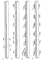
バッテリーは図23(A)に示す放電特性のように、放電時間に依存して出力電圧が低下する。図23(A)ではバッテリーの放電期間tallにおいて、充電完了直後の出力電圧をV1とすると、期間t1後に出力電圧がV2になる。期間t1の後、期間t2では一定の出力電圧V2が保持され、更に期間t3後に出力電圧はV3になる。期間t3の後は、バッテリーの放電特性がなくなる。 The output voltage of the battery decreases depending on the discharge time as shown in the discharge characteristics shown in FIG. In FIG. 23A, if the output voltage immediately after the completion of charging is V 1 in the discharge period t all of the battery, the output voltage becomes V 2 after the period t 1 . After a period t 1, is held output voltage V 2 of the constant in the period t 2 is the output voltage further after a period t 3 becomes V 3. After a period of time t 3, the discharge characteristics of the battery runs out.
バッテリーを備えた携帯型の電子機器における内部回路のクロック生成回路においては、図23(A)で示したバッテリーの経時的な出力電圧のV1からV3への低下により、クロック信号の周波数の低下を招いていた。図23(B)にクロック生成回路に入力される出力電圧のV1からV3への変化に伴う、発振周波数の変化について示す。図23(B)に示すように、クロック生成回路における発振周波数は、入力される電圧V1からV3に応じてF1からF3までばらつきを生じる。 In the clock generation circuit of the internal circuit in the portable electronic device including the battery, the frequency of the clock signal is reduced due to the decrease in the output voltage of the battery with time from V 1 to V 3 shown in FIG. It was causing a decline. FIG. 23B shows a change in oscillation frequency accompanying a change from V 1 to V 3 in the output voltage input to the clock generation circuit. As shown in FIG. 23B, the oscillation frequency in the clock generation circuit varies from F 1 to F 3 depending on the input voltages V 1 to V 3 .
発振周波数のばらつきの問題を解消するために、バッテリーの残量が一定となる図23(A)の期間t2の出力電圧V2をバッテリーの出力電圧として用いることで対応することができる。しかしながら、図23(A)のバッテリーの放電期間tallは、期間t2に比べて長くバッテリーの放電期間にはまだ期間t1、期間t3と余剰があった。 To eliminate variations in the problem of the oscillation frequency can be the battery level is addressed in the use of the output voltage V 2 of the time t 2 in FIG. 23 (A) to be constant as the output voltage of the battery. However, the battery discharge period t all in FIG. 23A is longer than the period t 2 , and the battery discharge period still has a surplus with the period t 1 and the period t 3 .
なおバッテリーの寿命を延ばすためには、特許文献2に記載の電子機器のようにクロック生成回路の発振周波数に基づいて、電子機器を駆動するモードを変更することによりバッテリーの蓄電残量を有効利用することも考えられる。しかし電子機器を駆動するモードにより駆動周波数を変動させることは、電子機器の品質の低下に繋がるといった課題も残る。
In order to extend the life of the battery, the remaining amount of power stored in the battery is effectively used by changing the mode for driving the electronic device based on the oscillation frequency of the clock generation circuit as in the electronic device described in
また携帯型の電子機器を駆動するためのクロック生成回路は、リングオシレータ等で構成される。リングオシレータは、上述のように、バッテリーより出力される電圧に応じて発振周波数が変わるため、リングオシレータの入力部において、レギュレータ等の定電圧回路を設ける必要があった。そのためクロック生成回路は、バッテリーの蓄電残量を有効に活用できていないといった課題があった。 In addition, a clock generation circuit for driving a portable electronic device includes a ring oscillator or the like. As described above, since the oscillation frequency of the ring oscillator changes according to the voltage output from the battery, it is necessary to provide a constant voltage circuit such as a regulator at the input portion of the ring oscillator. For this reason, the clock generation circuit has a problem in that it cannot effectively use the remaining amount of electricity stored in the battery.
そこで本発明は上記問題を鑑み、バッテリーの放電特性の変化に伴う出力電圧の変化によるクロック生成回路からの発振周波数の変動を抑制し、かつバッテリーの蓄電残量を有効利用することのできるクロック生成回路を提供することを課題とする。 Therefore, in view of the above problems, the present invention suppresses fluctuations in the oscillation frequency from the clock generation circuit due to changes in the output voltage due to changes in the discharge characteristics of the battery, and can effectively use the remaining amount of electricity stored in the battery. It is an object to provide a circuit.
上記目的を達成するために、本発明のクロック生成回路においては、バッテリーの出力電圧を検出するための出力電圧検出回路と、出力電圧検出回路で検出された出力電圧の値により分周数を判定する分周数判定回路と、出力電圧に応じた基準クロック信号を出力する発振回路と、基準クロック信号の波の数をカウントするカウンター回路と、基準クロック信号を分周する分周回路を有し、カウンター回路は、一旦分周回路に分周するための信号を出力した後、カウントした波の数が分周数に応じた波の数に達したら、分周回路に分周数判定回路で判定された分周数で分周するための信号を出力する構成とする。 To achieve the above object, in the clock generation circuit according to the present invention, the output voltage detection circuit for detecting the output voltage of the battery and the frequency division number are determined by the value of the output voltage detected by the output voltage detection circuit. A frequency division number determination circuit, an oscillation circuit that outputs a reference clock signal corresponding to the output voltage, a counter circuit that counts the number of waves of the reference clock signal, and a frequency division circuit that divides the reference clock signal After the counter circuit outputs a signal for frequency division to the frequency dividing circuit, when the number of counted waves reaches the number of waves corresponding to the frequency dividing number, the frequency dividing circuit is connected to the frequency dividing circuit. A signal is output for frequency division by the determined frequency division number.
本発明のクロック生成回路の一は、バッテリーの出力電圧を検出するための出力電圧検出回路と、出力電圧検出回路で検出された出力電圧の値により分周数を判定する分周数判定回路と、出力電圧に応じた基準クロック信号を出力する発振回路と、基準クロック信号の波の数をカウントするカウンター回路と、基準クロック信号を分周する分周回路を有し、カウンター回路は、一旦分周回路に分周するための信号を出力した後、カウントした波の数が分周数に応じた波の数に達したら、分周回路に分周数判定回路で判定された分周数で分周するための信号を出力することを特徴とする。 One of the clock generation circuits of the present invention includes an output voltage detection circuit for detecting an output voltage of a battery, a frequency division number determination circuit that determines a frequency division number based on the value of the output voltage detected by the output voltage detection circuit, and An oscillation circuit that outputs a reference clock signal according to the output voltage, a counter circuit that counts the number of waves of the reference clock signal, and a frequency divider circuit that divides the reference clock signal. After the signal for frequency division is output to the frequency divider circuit, when the number of counted waves reaches the number of waves corresponding to the frequency division number, the frequency division number is determined by the frequency division number determination circuit. A signal for frequency division is output.
別の本発明のクロック生成回路の一は、バッテリーの出力電圧を検出するための出力電圧検出回路と、出力電圧検出回路で検出された出力電圧の値により分周数を判定する分周数判定回路と、出力電圧に応じた基準クロック信号を出力する発振回路と、基準クロック信号の波の数をカウントするカウンター回路と、基準クロック信号を分周して得た信号をクロック信号として論理回路に出力する分周回路を有し、カウンター回路は、一旦分周回路に分周するための信号を出力した後、カウントした波の数が分周数に応じた波の数に達したら、分周回路に分周数判定回路で判定された分周数で分周するための信号を出力することを特徴とする。 Another clock generation circuit of the present invention includes an output voltage detection circuit for detecting the output voltage of the battery, and a frequency division number determination for determining the frequency division number based on the value of the output voltage detected by the output voltage detection circuit Circuit, an oscillation circuit that outputs a reference clock signal corresponding to the output voltage, a counter circuit that counts the number of waves of the reference clock signal, and a signal obtained by dividing the reference clock signal as a clock signal to the logic circuit After the output of the signal for frequency division to the frequency divider circuit, the counter circuit divides when the number of counted waves reaches the number of waves corresponding to the frequency division number. The circuit outputs a signal for frequency division by the frequency division number determined by the frequency division number determination circuit.
なお本発明のクロック生成回路におけるバッテリーは1次電池または2次電池であってもよい。 The battery in the clock generation circuit of the present invention may be a primary battery or a secondary battery.
なお本発明のクロック生成回路における発振回路は、リングオシレータ又は水晶発振器であってもよい。 Note that the oscillation circuit in the clock generation circuit of the present invention may be a ring oscillator or a crystal oscillator.
また本発明の半導体装置の一は、アンテナを備え、リーダ/ライタと無線通信により信号の送受信を行う半導体装置であって、クロック生成回路と、論理回路と、バッテリーと、を有し、クロック生成回路は、バッテリーの出力電圧を検出するための出力電圧検出回路と、出力電圧検出回路で検出された出力電圧の値により分周数を判定する分周数判定回路と、出力電圧に応じて基準クロック信号を出力する発振回路と、基準クロック信号の波の数をカウントするカウンター回路と、基準クロック信号を分周する分周回路を有し、カウンター回路は、一旦分周回路に分周するための信号を出力した後、カウントした波の数が分周数に応じた波の数に達したら、分周回路に分周数判定回路で判定された分周数で分周するための信号を出力することを特徴とする。 Another embodiment of the semiconductor device of the present invention is a semiconductor device that includes an antenna and transmits / receives a signal by wireless communication with a reader / writer. The semiconductor device includes a clock generation circuit, a logic circuit, and a battery. The circuit includes an output voltage detection circuit for detecting the output voltage of the battery, a frequency division number determination circuit for determining a frequency division number based on the value of the output voltage detected by the output voltage detection circuit, and a reference according to the output voltage An oscillation circuit that outputs a clock signal, a counter circuit that counts the number of waves of the reference clock signal, and a frequency dividing circuit that divides the reference clock signal, the counter circuit once divides the frequency into a frequency dividing circuit When the number of waves counted reaches the number of waves corresponding to the frequency division number, the signal for frequency division by the frequency division number determined by the frequency division number determination circuit is supplied to the frequency divider circuit. Output The features.
また別の本発明の半導体装置の一は、アンテナを備え、リーダ/ライタと無線通信により信号の送受信を行う半導体装置であって、クロック生成回路と、論理回路と、バッテリーと、を有し、クロック生成回路は、バッテリーの出力電圧を検出するための出力電圧検出回路と、出力電圧検出回路で検出された出力電圧の値により分周数を判定する分周数判定回路と、出力電圧に応じた基準クロック信号を出力する発振回路と、基準クロック信号の波の数をカウントするカウンター回路と、基準クロック信号を分周して得た信号をクロック信号として論理回路に出力する分周回路を有し、カウンター回路は、一旦分周回路に分周するための信号を出力した後、カウントした波の数が分周数に応じた波の数に達したら、分周回路に分周数判定回路で判定された分周数で分周するための信号を出力することを特徴とする。 Another semiconductor device of the present invention is a semiconductor device that includes an antenna and transmits / receives a signal by wireless communication with a reader / writer, and includes a clock generation circuit, a logic circuit, and a battery, The clock generation circuit includes an output voltage detection circuit for detecting the output voltage of the battery, a frequency division number determination circuit that determines the frequency division number based on the value of the output voltage detected by the output voltage detection circuit, and the output voltage according to the output voltage An oscillation circuit that outputs a reference clock signal, a counter circuit that counts the number of waves of the reference clock signal, and a frequency divider that outputs a signal obtained by dividing the reference clock signal to the logic circuit as a clock signal. The counter circuit once outputs a signal for frequency division to the frequency dividing circuit, and when the number of counted waves reaches the number of waves corresponding to the frequency dividing number, the frequency dividing circuit determines the frequency dividing number determination circuit. And outputs the signal to divide by is determined dividing number.
また本発明の半導体装置におけるバッテリーは、1次電池または2次電池であってもよい。 The battery in the semiconductor device of the present invention may be a primary battery or a secondary battery.
また本発明の半導体装置における発振回路は、リングオシレータ又は水晶発振器であってもよい。 Further, the oscillation circuit in the semiconductor device of the present invention may be a ring oscillator or a crystal oscillator.
本発明により、バッテリーの放電特性に伴う出力電圧の変化によるクロック生成回路からの発振周波数の変動を抑制し、かつバッテリーの蓄電残量を有効利用することのできるクロック生成回路を提供することができる。そのため、クロック信号のばらつきに起因した電子機器の品質の低下を引き起こすことなく、バッテリーの長寿命化を図ることができる。 According to the present invention, it is possible to provide a clock generation circuit that can suppress fluctuations in the oscillation frequency from the clock generation circuit due to a change in output voltage due to the discharge characteristics of the battery and can effectively use the remaining amount of charge in the battery. . Therefore, it is possible to extend the life of the battery without causing deterioration of the quality of the electronic device due to variations in the clock signal.
また本発明のクロック生成回路は、クロック生成回路の入力部にレギュレータ回路等の定電圧回路を設けることなく、ばらつきの小さいクロック信号を生成することができる。そのため、本発明のクロック生成回路を具備する電子機器等においては、低消費電力化及び電子機器の小型化をすることができる。 In addition, the clock generation circuit of the present invention can generate a clock signal with little variation without providing a constant voltage circuit such as a regulator circuit at the input of the clock generation circuit. Therefore, in an electronic device or the like including the clock generation circuit of the present invention, power consumption can be reduced and the electronic device can be reduced in size.
本発明の実施の形態について、図面を用いて以下に説明する。但し、本発明は以下の説明に限定されず、本発明の趣旨及びその範囲から逸脱することなくその形態及び詳細を様々に変更し得ることは当業者であれば容易に理解される。従って、本発明は以下に示す実施の形態の記載内容に限定して解釈されるものではない。なお、以下に説明する本発明の構成において、同じものを指す符号は異なる図面間で共通して用いる場合がある。
(実施の形態1)
Embodiments of the present invention will be described below with reference to the drawings. However, the present invention is not limited to the following description, and it is easily understood by those skilled in the art that modes and details can be variously changed without departing from the spirit and scope of the present invention. Therefore, the present invention should not be construed as being limited to the description of the embodiments below. Note that in the structures of the present invention described below, the same reference numerals may be used in common in different drawings.
(Embodiment 1)
本実施の形態では、本発明のクロック生成回路に関して図面を参照して説明する。 In this embodiment mode, a clock generation circuit of the present invention will be described with reference to the drawings.
図1に示す本発明のクロック生成回路100は、バッテリー111の出力電圧を検出するための出力電圧検出回路101と、バッテリー111の出力電圧に応じて基準クロック信号を出力する発振回路102と、出力電圧検出回路101で検出された出力電圧の値により分周数を判定する分周数判定回路103と、発振回路102より出力される基準クロック信号の波の数をカウントするカウンター回路104と、カウンター回路104に入力された波の数と分周数判定回路103より出力される分周数に応じて、基準クロック信号を分周することにより得られた信号をクロック信号として論理回路121に出力する分周回路105を有している。
The clock generation circuit 100 of the present invention shown in FIG. 1 includes an output
本発明は、バッテリーの放電特性により経時的な劣化に伴い出力電圧が低下した際においても、クロック信号の周波数の変動を抑制することができるといった効果を有する。当該効果は、出力電圧検出回路で検出するバッテリーの出力電圧の値に基づく分周数、及び発振回路から出力され、カウンター回路でカウントされた基準クロック信号の波の数に基づき、分周回路に入力される基準クロック信号を分周して出力することで実現することができる。以下、具体的な構成等について説明する。 The present invention has an effect that it is possible to suppress the variation in the frequency of the clock signal even when the output voltage decreases due to the deterioration over time due to the discharge characteristics of the battery. The effect is based on the frequency division number based on the output voltage value of the battery detected by the output voltage detection circuit and the number of waves of the reference clock signal output from the oscillation circuit and counted by the counter circuit. This can be realized by dividing and outputting the input reference clock signal. Hereinafter, a specific configuration and the like will be described.
図1に示した本発明のクロック生成回路100におけるバッテリー111からの出力電圧を検出するための出力電圧検出回路101に関して具体的な構成を図2に示す。図1に示した出力電圧検出回路101としては、一例として図2に示すように、反転比較回路を用いることができる。比較器201の反転入力端子にはバッテリー111からの出力電圧が入力され、比較器201の非反転入力端子にはVrefの電位が入力されている。バッテリー111からの出力電圧がVrefの電位よりも低いときには比較器201の出力からHレベルの信号が出力される。一方バッテリー111からの出力電圧がVrefの電位よりも高いときには比較器201の出力からLレベルの信号が出力される。バッテリー111からの出力電圧が複数段階に変化するのであれば図2に例示した反転比較回路を複数設け、論理回路により出力電圧に関する信号を分周数判定回路103に出力すればよい。こうして反転比較回路によりバッテリー111からの出力電圧の検出を行うことができる。
A specific configuration of the output
なお、本実施の形態では、一例として、バッテリー111からの出力電圧をV1、V2、V3の3段階を経るものとして説明し、V1>V2>V3であるとする。そのため、出力電圧検出回路101は、バッテリー111の出力電圧がV1、V2、またはV3かの情報について分周数判定回路103に出力するものとする。勿論本発明の出力電圧検出回路101は、検出される出力電圧がV1、V2、V3に限定されるものではなく、バッテリー111の出力電圧を検出し、バッテリー111の出力電圧に対応した信号を分周数判定回路103に出力するものであればよい。
In the present embodiment, as an example, the output voltage from the
また図1に示した本発明のクロック生成回路100におけるバッテリー111からの出力電圧により基準クロック信号を出力する発振回路102に関して具体的な構成を図3(A)に示す。図1に示した発振回路102としては、一例として図3(A)に示すように、Nチャネル型トランジスタ301とPチャネル型トランジスタ302が直列に接続され、この2つのトランジスタのゲートが接続されているインバータ構成を含み、このインバータを一単位としてこれを複数含んだ構成である。図3(A)に示す構成は所謂リングオシレータである。図3(A)において発振回路102は、5段構成であるが、これに限定されるものでない。複数のインバータは入力端子と出力端子が接続され、最終段の出力端子が初段のインバータの入力端子に接続されたループ構造している。このループ内のインバータの数について、発振回路102から信号を発振するためには、奇数個のインバータで構成される必要がある。
3A shows a specific configuration of the
なお、本発明においては図3(A)に示したリングオシレータを発振回路とするものに限定されるものではなく、水晶発振器であってもよい。すなわち、本発明の構成における発振回路は入力されるバッテリーの出力電圧に応じて発振する信号の周波数が異なるものであればよい。なおリングオシレータを構成するトランジスタを薄膜トランジスタで構成することにより、発振回路102の小型化を行うことができる。
In the present invention, the ring oscillator shown in FIG. 3A is not limited to the oscillation circuit, and a crystal oscillator may be used. That is, the oscillation circuit in the configuration of the present invention only needs to have a different frequency of the oscillating signal in accordance with the input output voltage of the battery. Note that when the transistor included in the ring oscillator is formed using a thin film transistor, the
なお本明細書においては、発振回路102から出力される信号を基準クロック信号という。また、クロック生成回路100より出力され、論理回路等を駆動する信号をクロック信号という。
In this specification, a signal output from the
また、発振回路102に入力されるバッテリー111の出力電圧V1、V2、またはV3に対する発振周波数の特性を図3(B)に示す。発振回路102はバッテリー111の出力電圧V1、V2、またはV3に対応した周波数F1、F2、またはF3の基準基ロック信号を出力する。なお、図示したように発振回路102における周波数はF1>F2>F3の関係を有する。入力されるバッテリー111の出力電圧が高ければ、発振回路102は高い周波数の信号を出力し、入力されるバッテリー111の出力電圧が低ければ、発振回路102は低い周波数の信号を出力する。
FIG. 3B shows the characteristics of the oscillation frequency with respect to the output voltage V 1 , V 2 , or V 3 of the
また図1に示した本発明のクロック生成回路100における分周数判定回路103は、出力電圧検出回路101から出力される、バッテリー111の出力電圧に関する信号に基づき、分周数を判定する回路である。分周数判定回路103は、出力電圧検出回路101から出力されるバッテリー111の出力電圧に関する信号に基づいて、分周数を判定し、当該分周数をカウンター回路104に出力することにより、カウンター回路104におけるカウンターをリセットするカウンター値を設定する。
In addition, the frequency division number determination circuit 103 in the clock generation circuit 100 of the present invention shown in FIG. 1 is a circuit that determines the frequency division number based on a signal relating to the output voltage of the
また図1に示した本発明のクロック生成回路100におけるカウンター回路104は、発振回路102から出力される基準クロック信号の波の数をカウントする回路である。カウンター回路104は、分周数判定回路103によって判定されたカウンターをリセットするカウンター値まで基準クロック信号の波の数をカウントする。カウンター回路104は、フリップフロップ回路等の論理回路を組み合わせて構成し、発振回路からの基準クロック信号が入力され、カウントが行われる。カウンター回路104は、カウントした波の数が分周数判定回路103によって判定されたカウンターをリセットするカウンター値に達した際に、分周回路105に信号を出力する。またカウンター回路104では、分周回路105への信号の出力と共に、カウンター値のリセットが行なわれる。
The counter circuit 104 in the clock generation circuit 100 of the present invention shown in FIG. 1 is a circuit that counts the number of waves of the reference clock signal output from the
また図1に示した本発明のクロック生成回路100における分周回路105は、カウンター回路104でカウントした波の数がカウンターをリセットするカウンター値に達した際に分周回路105に出力される信号をもとに、発振回路102から出力される基準クロック信号を分周する回路である。分周回路105は発振回路102が出力する基準クロック信号を、分周数判定回路103からのカウンター値がN(Nは自然数)であればN分周する回路である。
Further, the
なお本発明におけるバッテリーとは、放電または充電により、経時的に出力電圧が変化する電池のことをいう。そのため本実施の形態で用いられるバッテリー111としては、一次電池や二次電池が相当する。
The battery in the present invention refers to a battery whose output voltage changes with time due to discharging or charging. Therefore, the
次に図1に示したブロック図の具体的な動作についてタイミングチャート及びフローチャートを用いて説明をおこなう。 Next, a specific operation of the block diagram shown in FIG. 1 will be described using a timing chart and a flowchart.
図4においては、本実施の形態の構成について図1で示したブロック図におけるクロック生成回路100の動作の一例についてフローチャートを用いて説明する。図4のフローチャートにおいて、バッテリー111の出力電圧はV1以下かつV2よりも大きい範囲、V2以下かつV3よりも大きい範囲、またはV3のいずれかに含まれる例について説明する。またカウンター回路104におけるカウンター値をXとする。また出力電圧検出回路101から分周数判定回路103に出力される信号が、バッテリー111の出力電圧がV1以下かつV2よりも大きい範囲に含まれる際に示す信号であるとき、分周数判定回路103はカウンター回路104のカウンター数をX=3でリセットするものとして説明する。同様に、出力電圧検出回路101から分周数判定回路103に出力される信号が、バッテリー111の出力電圧がV2以下かつV3よりも大きい範囲に含まれる際に示す信号であるとき、分周数判定回路103はカウンター回路104のカウンター数をX=2でリセットするものとして説明する。また同様に出力電圧検出回路101から分周数判定回路103に出力される信号が、バッテリー111の出力電圧がV3の際に示す信号であるとき、分周数判定回路103はカウンター回路104のカウンター数をX=1でリセットするものとして説明する。
In FIG. 4, an example of the operation of the clock generation circuit 100 in the block diagram shown in FIG. 1 is described with reference to a flowchart of the structure of this embodiment. In the flowchart of FIG. 4, an example in which the output voltage of the
まず、カウンター回路104は、発振回路102から出力される基準クロック信号の波の数をカウントする前にカウンター値をリセットする(図4のステップS401)。カウンター値をリセットすることにより、カウンター値Xは0(X=0)となる。カウンター値のリセットは、カウンター回路104に入力される分周数判定回路103からの信号に基づいて決定されたカウンター値に達した際にリセットされるものである。 First, the counter circuit 104 resets the counter value before counting the number of waves of the reference clock signal output from the oscillation circuit 102 (step S401 in FIG. 4). By resetting the counter value, the counter value X becomes 0 (X = 0). The counter value is reset when a counter value determined based on a signal from the frequency division number determination circuit 103 input to the counter circuit 104 is reached.
次にカウンター回路104は、発振回路102からの基準クロック信号のカウントを開始する(ステップS402)。カウンター値はリセット後にカウンター回路に入力された基準クロック信号の波の数であるため、1波長毎にカウンター値に1を加算していく。すなわちカウンター回路104には、基準クロック信号の1波長分が入力されるごとにカウンター値に1が加算されていき、波の数のカウントが行われることになる。
Next, the counter circuit 104 starts counting the reference clock signal from the oscillation circuit 102 (step S402). Since the counter value is the number of waves of the reference clock signal input to the counter circuit after reset, 1 is added to the counter value for each wavelength. That is, every time one wavelength of the reference clock signal is input to the
カウンター回路104において、カウントを開始すると共に、カウンター回路104に入力される分周数判定回路103からの信号を決める出力電圧検出回路101で検出されたバッテリー111の出力電圧がV1以下かつV2よりも大きい範囲内にあるかどうかの判定が行われる(ステップS403)。カウンター回路104に入力される分周数判定回路103からの信号を決める出力電圧検出回路101で検出されたバッテリー111の出力電圧がV1以下かつV2よりも大きい範囲内にあれば、カウンター値が3(X=3)であるか否かの判断が行われる(ステップS404)。ステップS404において、カウンター値がX=3でなければ、再度ステップS402に戻り、カウンター値の加算が行われる。ステップS404において、カウンター値がX=3であれば、信号を分周回路105に出力し(ステップS405)、カウンター回路104のカウンター値をリセットするステップS401に戻る。
In the counter circuit 104, and starts counting, the counter circuit 104 frequency division number is input to the determination circuit 103 determines the signal from the output
ステップS403で、カウンター回路104に入力される分周数判定回路103からの信号を決める出力電圧検出回路101で検出されたバッテリー111の出力電圧がV1以下かつV2よりも大きい範囲内になければ、バッテリー111の出力電圧がV2以下かつV3よりも大きい範囲内にあるかどうかの判定が行われる(ステップS406)。カウンター回路104に入力される分周数判定回路103からの信号を決める出力電圧検出回路101で検出されたバッテリー111の出力電圧がV2であれば、カウンター値が2(X=2)であるかの判断が行われる(ステップS407)。ステップS407において、カウンター値がX=2でなければ、再度ステップS402に戻り、カウンター値の加算が行われる。ステップS407において、カウンター値がX=2であれば、ステップS405に移行し、カウンター回路のカウンター値をリセットするステップS401に戻る。
In step S403, be within the output voltage is greater than V 1 or less and V 2 of the
ステップS406で、カウンター回路104に入力される分周数判定回路103からの信号を決める出力電圧検出回路101でのバッテリー111の出力電圧がV2以下かつV3よりも大きい範囲内になければ、バッテリー111の出力電圧がV3であるかどうかの判定が行われる(ステップS408)。カウンター回路104に入力される分周数判定回路103からの信号を決める出力電圧検出回路101でのバッテリー111の出力電圧がV3であれば、カウンター値が1(X=1)になった際に(ステップS409)、ステップS405に移行し、カウンター回路104のカウンター値をリセットするステップS401に戻る。
In step S406, if the output voltage of the
ステップS408で、カウンター回路104に入力される分周数判定回路103からの信号を決める出力電圧検出回路101でのバッテリー111の出力電圧がV3でなければ、クロック生成回路100は、この時バッテリー111はクロック信号を発振する十分な蓄電残量を有さず、クロック信号の発振が停止される(ステップS410)。
In step S408, unless the output voltage V 3 of the
次に、上述した図4のフローチャートで説明した図1の構成に関する動作のタイミングチャートについて図5を参照して説明する。 Next, an operation timing chart related to the configuration of FIG. 1 described in the flowchart of FIG. 4 will be described with reference to FIG.
図5には、バッテリー111の出力電圧がV1、V2、またはV3であるときの発振回路102から出力される基準クロック信号、カウンター回路104におけるカウンター値、及びクロック生成回路100から出力されるクロック信号のタイミングチャートを示している。
In FIG. 5, the reference clock signal output from the
バッテリー111の出力電圧はV1、V2、V3と経時的に変化する。そのため、基準クロック信号の周波数は図3(B)に示したように、V1、V2、V3の変化に依存して下がる。そのため、図5に示す基準クロック信号の周波数もV1、V2、V3の変化に依存して下がる。また図5において、上述したようにカウンター値は出力電圧V1のときX=3でリセットし、出力電圧V2のときX=2でリセットし、出力電圧V3のときX=1でリセットするものとして図示している。
The output voltage of the
図5に示すタイミングチャートを図4で説明したフローチャートに沿って説明する。図4のステップS401においてカウンター値がリセットされる。ステップS401の後に、図4のステップS402において、バッテリーの出力電圧がV1、V2、またはV3であるときの基準クロック信号の波の数に依存してバッテリー111の出力電圧がV1、V2、またはV3であるときのカウンター値が1ずつ加算されている。バッテリーの出力電圧がV1のとき(図4のステップS403)、カウンター回路104は、カウンター値が3(図4のステップS404)で分周回路105に、分周するための信号を出力する(図4のステップS405)。分周回路105は、カウンター回路104より出力された分周するための信号に基づき、基準クロック信号に分周を行う。
The timing chart shown in FIG. 5 will be described along the flowchart described in FIG. In step S401 of FIG. 4, the counter value is reset. After step S401, in step S402 in FIG. 4, the output voltage of the
同様にバッテリー111の出力電圧がV2のとき(図4のステップS406)、カウンター回路104は、カウンター値が2(図4のステップS407)で分周回路105に信号を出力する(図4のステップS405)。分周回路105は、カウンター回路104より出力された信号に基づき、基準クロック信号に分周を行う。
Similarly, when the output voltage of the
同様にバッテリー111の出力電圧がV3のとき(図4のステップS408)、カウンター回路104は、カウンター値が1(図4のステップS409)で分周回路105に信号を出力する(図4のステップS405)。分周回路105は、カウンター回路104より出力された信号に基づき、基準クロック信号に分周を行う。
Similarly, when the output voltage of the
本実施の形態においては、バッテリー111の出力電圧がV1のときにカウンター回路104より信号が出力されると、分周回路105は基準クロック信号を3分周するものとして説明している。また本実施の形態においては、バッテリー111の出力電圧がV2のときにカウンター回路104よりカウンター値が出力されると、分周回路105は基準クロック信号を2分周するものとして説明している。また、本実施の形態においては、バッテリー111の出力電圧がV3のときにカウンター回路104よりカウンター値が出力されると、分周回路105は基準クロック信号を1分周するものとして説明している。
In the present embodiment, when the output voltage of the
本発明においては基準クロック信号の波の数をカウンター回路でカウントし、バッテリーの出力電圧に応じた分周数で分周するための信号を分周回路に出力することによって、分周回路にて当該カウンター値に応じた分周を行うことができる。そのためクロック生成回路において、図5に示すとおり、出力するクロック信号の周波数が、バッテリーの出力電圧V1、V2、V3に依存して大きく変化することなく、出力することが可能になる。そのためクロック信号のばらつきに起因した電子機器の品質の低下を引き起こすことなく、バッテリーの蓄電残量を有効利用することができる。 In the present invention, the number of waves of the reference clock signal is counted by a counter circuit, and a signal for frequency division by a frequency division number corresponding to the output voltage of the battery is output to the frequency divider circuit. Frequency division according to the counter value can be performed. Therefore, in the clock generation circuit, as shown in FIG. 5, the frequency of the output clock signal can be output without largely changing depending on the output voltages V 1 , V 2 , and V 3 of the battery. Therefore, the remaining amount of power stored in the battery can be effectively used without causing deterioration of the quality of the electronic device due to variations in the clock signal.
従来は、バッテリーと発振回路の間にレギュレータ回路等の定電圧回路を設けることで、クロック生成回路からのクロック信号の周波数のばらつきを低減させていた。本発明においては、定電圧回路を設けることなく、周波数の変動の少ないクロック信号を出力することが可能になる。そのため、本発明においては定電圧回路を用いる場合に比べて電子機器の小型化が可能になり、回路の設計面積が限られた場合の電子機器等においては特に有用である。 Conventionally, by providing a constant voltage circuit such as a regulator circuit between the battery and the oscillation circuit, variation in the frequency of the clock signal from the clock generation circuit has been reduced. In the present invention, it is possible to output a clock signal with little frequency fluctuation without providing a constant voltage circuit. Therefore, in the present invention, it is possible to reduce the size of the electronic device as compared with the case where a constant voltage circuit is used, and the present invention is particularly useful in an electronic device or the like when the circuit design area is limited.
なお、本発明においては、カウンター値に対応する分周数の値は限定されるものではなく、適宜クロック信号の周波数に基づいて分周数を決定すればよい。 In the present invention, the value of the frequency division number corresponding to the counter value is not limited, and the frequency division number may be determined as appropriate based on the frequency of the clock signal.
以上のように、本発明はバッテリーの放電特性に伴う出力電圧の変化による、クロック生成回路から出力されるクロック信号の発振周波数の変化を抑制し、かつバッテリーの蓄電残量を有効利用することのできるクロック生成回路を提供することができる。そのため、クロック信号のばらつきに起因した電子機器の品質の低下を引き起こすことなく、バッテリーの長寿命化を図ることができる。 As described above, the present invention suppresses the change in the oscillation frequency of the clock signal output from the clock generation circuit due to the change in the output voltage due to the discharge characteristics of the battery, and effectively uses the remaining battery charge of the battery. A clock generation circuit that can be provided can be provided. Therefore, it is possible to extend the life of the battery without causing deterioration of the quality of the electronic device due to variations in the clock signal.
また本発明のクロック生成回路は、クロック生成回路の入力部にレギュレータ回路等の定電圧回路を設けることなく、周波数のばらつきの小さいクロック信号を生成することができる。そのため、本発明のクロック生成回路を具備する電子機器等においては、低消費電力化及び電子機器の小型化をすることができる。 Further, the clock generation circuit of the present invention can generate a clock signal with small frequency variation without providing a constant voltage circuit such as a regulator circuit at the input of the clock generation circuit. Therefore, in an electronic device or the like including the clock generation circuit of the present invention, power consumption can be reduced and the electronic device can be reduced in size.
なお、本実施の形態は、本明細書の他の実施の形態の技術的要素と組み合わせて行うことができる。
(実施の形態2)
Note that this embodiment can be implemented in combination with the technical elements of the other embodiments in this specification.
(Embodiment 2)
本実施の形態では、上記実施の形態で示したクロック生成回路を有し、且つ無線で情報の送受信が可能な半導体装置に関して図面を参照して説明する。 In this embodiment, a semiconductor device including the clock generation circuit described in the above embodiment and capable of transmitting and receiving information wirelessly will be described with reference to drawings.
近年、超小型ICチップと、無線通信用のアンテナを組み合わせたRFタグ等の半導体装置が脚光を浴びている。RFタグは、無線通信装置(リーダ/ライタともいう)を使った通信信号(動作磁界)の授受により、データを書き込んだり、データを読み出すことができる。 In recent years, a semiconductor device such as an RF tag in which an ultra-small IC chip and an antenna for wireless communication are combined is in the spotlight. The RF tag can write and read data by transmitting and receiving a communication signal (operation magnetic field) using a wireless communication device (also referred to as a reader / writer).
RFタグ等の無線で情報の送受信が可能な半導体装置の応用分野として、例えば、流通業界における商品管理が挙げられる。現在では、バーコードなどを利用した商品管理が主流であるが、バーコードは光学的に読み取るため、遮蔽物があるとデータを読み取れない。一方、RFタグでは、無線でデータを読み取るため、遮蔽物があっても読み取れる。従って、商品管理の効率化、低コスト化などが実現可能である。その他、乗車券、航空旅客券、料金の自動精算など、広範な応用が実現可能である。 As an application field of a semiconductor device capable of transmitting and receiving information wirelessly such as an RF tag, for example, merchandise management in the distribution industry can be cited. At present, merchandise management using bar codes and the like is the mainstream, but since bar codes are optically read, data cannot be read if there is a shield. On the other hand, since the RF tag reads data wirelessly, it can be read even if there is a shield. Therefore, it is possible to realize efficient merchandise management and cost reduction. In addition, a wide range of applications such as boarding tickets, air passenger tickets, and automatic payment of fare are possible.
本実施の形態では、本発明における半導体装置の一例として、図6を用いて説明する。図6は、RFタグのブロック図である。 In this embodiment, an example of a semiconductor device of the present invention will be described with reference to FIGS. FIG. 6 is a block diagram of the RF tag.
図6のRFタグ600では、アンテナ601によって受信された通信信号が信号処理回路604における復調回路605に入力される。通常、通信信号は13.56MHz、915MHzなどのキャリアがASK(振幅偏移;Amplitude shift keying)変調、FSK(周波数偏移;Frequency shift keying)変調などの処理を受けた上で送られてくる。図6において、信号処理回路604が信号を処理するためには基準となるクロック信号が必要であり、クロック生成回路603に入力されるバッテリー602からの出力電圧により得られ、クロック生成回路603から出力されるクロック信号を用いている。また図6においては、信号処理回路604を駆動するための電力もバッテリー602より供給されている。ASK変調やPSK変調された通信信号は復調回路605で復調される。復調後の信号は、論理回路606に送られ解析される。論理回路606で解析された信号はメモリコントロール回路607に送られ、それに基づき、メモリコントロール回路607はメモリ回路608を制御し、メモリ回路608に記憶されたデータを取り出し論理回路609に送られる。論理回路609でエンコード処理されたのち、変調回路610はキャリアに変調をかける。
In the
次に、図7を用いて、図6で示したRFタグ600の模式図について説明する。なお、図7において、図6に相当する部分には、同一の番号を付し、説明を省略する。なお図6で示したクロック生成回路は、図7では信号処理回路と同じ基板上に形成されるものとして以下説明を行う。
Next, a schematic diagram of the
図7(a)に示すRFタグ600は、基板701上に、アンテナ601、バッテリー602、クロック生成回路603、及び信号処理回路604を有している。アンテナ601は接続端子720及び接続端子721を備えている。アンテナ601においては、接続端子720及び接続端子721のそれぞれが信号処理回路604と接続されている。
An
信号処理回路604に含まれるトランジスタは、様々な形態のトランジスタを適用させることが出来る。よって、適用可能なトランジスタの種類に限定はない。したがって、非晶質シリコンや多結晶シリコンに代表される非単結晶半導体膜を用いた薄膜トランジスタ(TFT)、半導体基板やSOI基板を用いて形成されるトランジスタ、MOS型トランジスタ、接合型トランジスタ、バイポーラトランジスタ、ZnO、a−InGaZnOなどの化合物半導体を用いたトランジスタ、有機半導体やカーボンナノチューブを用いたトランジスタ、その他のトランジスタを適用することができる。なお、非単結晶半導体膜には水素またはハロゲンが含まれていてもよい。 Various types of transistors can be used as the transistor included in the signal processing circuit 604. Thus, there is no limitation on the type of applicable transistor. Therefore, a thin film transistor (TFT) using a non-single-crystal semiconductor film typified by amorphous silicon or polycrystalline silicon, a transistor formed using a semiconductor substrate or an SOI substrate, a MOS transistor, a junction transistor, or a bipolar transistor Alternatively, a transistor using a compound semiconductor such as ZnO or a-InGaZnO, a transistor using an organic semiconductor or a carbon nanotube, or another transistor can be used. Note that the non-single-crystal semiconductor film may contain hydrogen or halogen.
基板701の種類は、様々なものを用いることができ、特定のものに限定されることはない。従って例えば、単結晶基板、SOI基板、ガラス基板、石英基板、プラスチック基板などを用いることが出来る。また、ある基板に信号処理回路604を形成し、その後、別の基板に信号処理回路604を移動させて、別の基板上に配置するようにしてもよい。 Various types of substrates 701 can be used, and the substrate 701 is not limited to a specific type. Therefore, for example, a single crystal substrate, an SOI substrate, a glass substrate, a quartz substrate, a plastic substrate, or the like can be used. Alternatively, the signal processing circuit 604 may be formed on a certain substrate, and then the signal processing circuit 604 may be moved to another substrate and placed on another substrate.
アンテナ601の形状については、特に限定されない。たとえば図8(A)のように基板801上の信号処理回路802を囲むように一面のアンテナ803を配置しても良い。また、図8(B)のように基板801上の信号処理回路802の周りに細いアンテナ803を配置しても良い。また、図8(C)のように高周波の電磁波を受信するための形状をとってもよい。また、図8(D)のように180度無指向性の形状をとってもよい。また、図8(E)のように棒状に長く伸ばした形状をとってもよい。また、例えば、いわゆる、ダイポールアンテナ、ループアンテナ、八木アンテナ、パッチアンテナ又は微小アンテナなどの形状をとってもよい。
The shape of the
なお、図8においては、説明を簡単にするため、バッテリーに相当するものは記載されていないが本発明のクロック生成回路を具備する半導体装置には、バッテリーが設けられる。 In FIG. 8, for the sake of simplicity, the equivalent of a battery is not shown, but a semiconductor device including the clock generation circuit of the present invention is provided with a battery.
図7(a)に示すアンテナ601は、信号処理回路604が形成された基板上に形成されていてもよいし、信号処理回路604の形成された基板とは別の基板上に形成してもよい。そして、アンテナ601を形成する基板の種類は、様々なものを用いることができ、特定のものに限定されることはない。従って例えば、単結晶基板、SOI基板、ガラス基板、石英基板、プラスチック基板などに形成することが出来る。そして、アンテナ601を信号処理回路604の形成された基板と同じ基板に形成する場合には、スパッタリング法や、CVD法、スピンコーティング法などにより導電膜を形成し、導電膜をパターニングしてアンテナ601を形成してもよいし、インクジェット法に代表される液滴吐出法又はスクリーン印刷法などによりアンテナ601を形成してもよい。アンテナ601を信号処理回路604の形成された基板と別の基板に形成する場合にも上述した方法によりアンテナ601を形成することができるが、好ましくは、特にスクリーン印刷法によりアンテナ601を形成するとよい。
The
なお、信号処理回路604の形成された基板とアンテナ601との接続は公知の方法で行うことができる。例えばアンテナと信号処理回路とをワイヤボンディング接続やバンプ接続を用いて接続する、あるいはチップ化した信号処理回路の形成された基板一面を電極にしてアンテナに貼り付けるという方法を取ってもよい。この方式ではACF(anisotropic conductive film;異方性導電性フィルム)を用いて貼り付けることができる。
Note that connection between the substrate over which the signal processing circuit 604 is formed and the
また、アンテナに必要な長さは受信に用いる周波数によって適正な長さが異なる。そのため、一般には波長の整数分の1の長さにし、例えば周波数が2.45GHzの場合は約60mm(1/2波長)、約30mm(1/4波長)とすれば良い。 The length required for the antenna differs depending on the frequency used for reception. For this reason, the length is generally set to 1 / integer of the wavelength. For example, when the frequency is 2.45 GHz, the length may be about 60 mm (1/2 wavelength) and about 30 mm (1/4 wavelength).
また、図7(a)において、アンテナ601は信号処理回路604と共に同じ基板上に積層して設ける構成としているが、外付けのアンテナとして設けられるものであっても良い。なお、図7(a)に示すようにアンテナ601を信号処理回路604と共に同じ基板701上に積層して設ける場合には、好ましくは、アンテナ形状を微小ループアンテナや、微小ダイポールアンテナなどの形状のアンテナとするとよい。
In FIG. 7A, the
バッテリー602には、1次電池または2次電池であれば適用可能である。また、本発明のクロック生成回路は、経時的に放電特性が変化することにより、出力電圧が変化するバッテリーを具備する半導体装置であれば適用可能である。
The
なお、本発明のクロック生成回路を具備する半導体装置の構成としては、図7(a)に示すものに限られない。たとえば、図7(b)には、アンテナ601とバッテリー602との間に信号処理回路604が配置されている構成を示しているが、アンテナ601と信号処理回路604との間にバッテリー602が配置されていてもよいし、バッテリー602と信号処理回路604との間にアンテナ601が配置されていてもよい。また、アンテナ601とバッテリー602と信号処理回路604との面積比もこれに限られるものではない。つまり、本発明のクロック生成回路を具備する半導体装置は、断面から層別に見たときに、アンテナ601とバッテリー602と信号処理回路604との位置関係は限定されない。また、アンテナ601と信号処理回路604とがそれぞれ別の基板に形成されていてもよいし、アンテナ601と信号処理回路604とバッテリー602とが同じ基板上に形成されていてもよい。
Note that the configuration of the semiconductor device including the clock generation circuit of the present invention is not limited to that shown in FIG. For example, FIG. 7B shows a configuration in which the signal processing circuit 604 is disposed between the
なお、本実施の形態は、本明細書の他の実施の形態の技術的要素と組み合わせて実施することができる。すなわち本実施の形態は、バッテリーの放電特性に伴う出力電圧の変化によるクロック生成回路から出力されるクロック信号の発振周波数の変化を抑制し、かつバッテリーの蓄電残量を有効利用することのできるクロック生成回路を具備する半導体装置を提供することができる。そのため、クロック信号のばらつきに起因した電子機器の品質の低下を引き起こすことなく、バッテリーの長寿命化を図ることができる。 Note that this embodiment can be implemented in combination with the technical elements of the other embodiments in this specification. In other words, this embodiment suppresses a change in the oscillation frequency of the clock signal output from the clock generation circuit due to a change in the output voltage due to the discharge characteristics of the battery, and can effectively use the remaining amount of charge in the battery. A semiconductor device including the generation circuit can be provided. Therefore, it is possible to extend the life of the battery without causing deterioration of the quality of the electronic device due to variations in the clock signal.
また本発明のクロック生成回路を具備する半導体装置は、クロック生成回路の入力部にレギュレータ回路等の定電圧回路を設けることなく、周波数のばらつきの小さいクロック信号を生成することができる。そのため、本発明のクロック生成回路を具備する半導体装置においては、低消費電力化及び半導体装置の小型化をすることができる。
(実施の形態3)
In addition, a semiconductor device including the clock generation circuit of the present invention can generate a clock signal with small variation in frequency without providing a constant voltage circuit such as a regulator circuit at an input portion of the clock generation circuit. Therefore, in a semiconductor device including the clock generation circuit of the present invention, power consumption can be reduced and the semiconductor device can be reduced in size.
(Embodiment 3)
本実施の形態では、上記実施の形態で示した半導体装置において、電磁波により充電可能なバッテリーを設けた半導体装置の一例に関して図面を参照して説明する。 In this embodiment, an example of a semiconductor device provided with a battery that can be charged by electromagnetic waves in the semiconductor device described in the above embodiment will be described with reference to drawings.
本実施の形態で示す半導体装置に関して図9に示すRFタグを例にして説明する。 The semiconductor device described in this embodiment is described using the RF tag illustrated in FIG. 9 as an example.
図9に示すRFタグ600は、アンテナ601、バッテリー602、クロック生成回路603、信号処理回路604、充放電回路900を有している。
An
充放電回路900は、整流回路901、充電制御回路902、放電制御回路903を有している。また、信号処理回路604は、復調回路605、論理回路606、メモリコントロール回路607、メモリ回路608、論理回路609、変調回路610によって構成される。なお、上記実施の形態2における図6の構成との違いは、RFタグ600に充放電回路900が設けられた点にある。
The charge / discharge circuit 900 includes a
信号処理回路604は、リーダ/ライタ951より送信されアンテナ601により受信された通信信号が、信号処理回路604における復調回路605に入力される。通常、通信信号は13.56MHz、915MHzなどのキャリアをASK変調、PSK変調などの処理を受けた後送られてくる。例えば、通信信号を13.56MHzとする場合は、バッテリー602を充電するためのリーダ/ライタからの電磁波の周波数も同じであることが望ましい。なお充電のための信号と、通信のための信号とを同一の周波数帯にすることでアンテナ601を共有にすることができる。アンテナ601を共有化することにより、半導体装置の小型化を達成することができる。
In the signal processing circuit 604, a communication signal transmitted from the reader /
図9において、信号処理回路604が信号を処理するためには基準となるクロック信号が必要であり、バッテリー602からの出力電圧が放電制御回路903を介してクロック生成回路603に入力され、クロック生成回路603から出力されるクロック信号を用いている。また図9においては、信号処理回路604を駆動するための電源もバッテリー602より放電制御回路903を介して供給されている。ASK変調やPSK変調された通信信号は復調回路605で復調される。復調後の信号は、論理回路606に送られ解析される。論理回路606で解析された信号はメモリコントロール回路607に送られ、それに基づき、メモリコントロール回路607はメモリ回路608を制御し、メモリ回路608に記憶されたデータを取り出し論理回路609に送られる。論理回路609でエンコード処理されたのち、変調回路610はキャリアに変調をかける。
In FIG. 9, the signal processing circuit 604 needs a reference clock signal in order to process the signal, and the output voltage from the
また図9において、アンテナ601がリーダ/ライタ951からバッテリー602を充電するための電磁波を受信した場合の動作の一例について説明する。なお本実施の形態においては、充電制御回路902に第1のスイッチが設けられ、放電制御回路903に第2のスイッチが設けられている例を示す。
In FIG. 9, an example of an operation when the
まず、リーダ/ライタ951から電磁波が送信されると、アンテナ601がリーダ/ライタ951から送信された電磁波の受信を開始する。そして、バッテリー602の電力を他の回路へ供給しないように放電制御回路903に設けられた第2のスイッチをオフにする。
First, when an electromagnetic wave is transmitted from the reader /
次に、充電制御回路902に設けられた第1のスイッチがオンして、整流回路901を介して整流化及び平滑化された信号により、バッテリー602の充電が開始される。そして、バッテリー602の電圧が所定の電圧値以上になった場合に、充電制御回路902に設けられた第1のスイッチをオフし、充電を停止する。
Next, the first switch provided in the charging control circuit 902 is turned on, and charging of the
次に、第1のスイッチのオフと同時又はその後に第2のスイッチをオンして、放電制御回路903を介して信号処理回路604及びクロック生成回路603に電力を供給し、RFタグ600は、通信を開始する信号が含まれた電磁波(以下、単に「信号」と記す場合がある)をリーダ/ライタ951に送信する。
Next, simultaneously with or after the first switch is turned off, the second switch is turned on to supply power to the signal processing circuit 604 and the
なお、図9に示した構成では、充放電回路900と信号処理回路604にアンテナ601を共有させて設けた場合を示したが、充放電回路900と信号処理回路604にそれぞれアンテナを設けた構成としてもよい。例えば充放電回路900に第1のアンテナ回路を設け、信号処理回路604に第2のアンテナ回路をそれぞれ設けた構成でもよい。なお、充放電回路900に第1のアンテナ回路を設け、信号処理回路604に第2のアンテナ回路をそれぞれ設けることで、第1のアンテナ回路には外部に無作為に生じている電磁波を受信させ、第2のアンテナ回路にはリーダ/ライタ951から発振された特定の波長を有する電磁波を受信させることができる。
In the configuration illustrated in FIG. 9, the charging / discharging circuit 900 and the signal processing circuit 604 are provided with the
以上のように、無線で充電可能なバッテリーを設けることによって、半導体装置に設けられたバッテリーの充電を容易に行うことが可能となる。また、一定の時間をかけて電磁波を受信してバッテリーの充電を行い、蓄電された電力をパルス的に放電することによって、バッテリーの充電に利用する電磁波が微弱な場合であっても、バッテリーから負荷部に大きい電力を供給することができる。 As described above, by providing a wirelessly chargeable battery, the battery provided in the semiconductor device can be easily charged. Also, by receiving electromagnetic waves over a certain period of time and charging the battery, and discharging the stored power in a pulsed manner, even if the electromagnetic waves used for charging the battery are weak, Large electric power can be supplied to the load section.
なお、本実施の形態は、本明細書の他の実施の形態の技術的要素と組み合わせて行うことができる。すなわち本実施の形態は、バッテリーの放電特性に伴う出力電圧の変化によるクロック生成回路からの発振周波数の変化を抑制し、かつバッテリーの蓄電残量を有効利用することのできるクロック生成回路を具備する半導体装置を提供することができる。そのため、クロック信号のばらつきに起因した電子機器の品質の低下を引き起こすことなく、バッテリーの長寿命化を図ることができる。 Note that this embodiment can be implemented in combination with the technical elements of the other embodiments in this specification. That is, the present embodiment includes a clock generation circuit that can suppress a change in the oscillation frequency from the clock generation circuit due to a change in the output voltage due to the discharge characteristics of the battery and can effectively use the remaining amount of charge in the battery. A semiconductor device can be provided. Therefore, it is possible to extend the life of the battery without causing deterioration of the quality of the electronic device due to variations in the clock signal.
また本発明のクロック生成回路を具備する半導体装置は、クロック生成回路の入力部にレギュレータ回路等の定電圧回路を設けることなく、ばらつきの小さいクロック信号を生成することができる。そのため、本発明のクロック生成回路を具備する半導体装置においては、低消費電力化及び半導体装置の小型化をすることができる。 In addition, a semiconductor device including the clock generation circuit of the present invention can generate a clock signal with little variation without providing a constant voltage circuit such as a regulator circuit at an input portion of the clock generation circuit. Therefore, in a semiconductor device including the clock generation circuit of the present invention, power consumption can be reduced and the semiconductor device can be reduced in size.
本実施例では、上記実施の形態で示した半導体装置の作製方法の一例に関して、図面を参照して説明する。本実施例においては、半導体装置におけるアンテナ、バッテリー、信号処理回路を同一基板上に薄膜トランジスタを用いて設ける構成について説明する。なお、基板上に一度にアンテナ、バッテリー、信号処理回路を形成することで、小型化を図ることができるため好適である。また、バッテリーとしては薄膜の二次電池を用いた例について説明する。 In this example, an example of a method for manufacturing the semiconductor device described in the above embodiment is described with reference to drawings. In this embodiment, a structure in which an antenna, a battery, and a signal processing circuit in a semiconductor device are provided using a thin film transistor over the same substrate will be described. Note that it is preferable to form the antenna, the battery, and the signal processing circuit over the substrate at a time because the size can be reduced. An example in which a thin film secondary battery is used as the battery will be described.
まず、基板1301の一表面に絶縁膜1302を介して剥離層1303を形成し、続けて下地膜として機能する絶縁膜1304と半導体膜1305(例えば、非晶質珪素を含む膜)を積層して形成する(図10(A)参照)。なお、絶縁膜1302、剥離層1303、絶縁膜1304および半導体膜1305は、連続して形成することができる。
First, a
基板1301は、ガラス基板、石英基板、金属基板(例えばセラミック基板またはステンレス基板など)、Si基板等の半導体基板などから選択されるものである。他にもプラスチック基板として、ポリエチレンテレフタレート(PET)、ポリエチレンナフタレート(PEN)、ポリエーテルサルフォン(PES)、アクリルなどの基板を選択することもできる。なお、本工程では、剥離層1303は、絶縁膜1302を介して基板1301の全面に設けているが、必要に応じて、基板1301の全面に剥離層を設けた後に、フォトリソグラフィ法により選択的に設けてもよい。
The
絶縁膜1302、絶縁膜1304は、CVD法やスパッタリング法等を用いて、酸化シリコン、窒化シリコン、酸化窒化シリコン(SiOxNy)(x>y>0)、窒化酸化シリコン(SiNxOy)(x>y>0)等の絶縁材料を用いて形成する。例えば、絶縁膜1302、1304を2層構造とする場合、第1層目の絶縁膜として窒化酸化シリコン膜を形成し、第2層目の絶縁膜として酸化窒化シリコン膜を形成するとよい。また、第1層目の絶縁膜として窒化シリコン膜を形成し、第2層目の絶縁膜として酸化シリコン膜を形成してもよい。絶縁膜1302は、基板1301から剥離層1303又はその上に形成される素子に不純物元素が混入するのを防ぐブロッキング層として機能し、絶縁膜1304は基板1301、剥離層1303からその上に形成される素子に不純物元素が混入するのを防ぐブロッキング層として機能する。このように、ブロッキング層として機能する絶縁膜1302、1304を形成することによって、基板1301からNaなどのアルカリ金属やアルカリ土類金属が、剥離層1303から剥離層に含まれる不純物元素がこの上に形成する素子に悪影響を与えることを防ぐことができる。なお、基板1301として石英を用いるような場合には絶縁膜1302、1304を省略してもよい。
The insulating
剥離層1303は、金属膜や金属膜と金属酸化膜の積層構造等を用いることができる。金属膜としては、タングステン(W)、モリブデン(Mo)、チタン(Ti)、タンタル(Ta)、ニオブ(Nb)、ニッケル(Ni)、コバルト(Co)、ジルコニウム(Zr)、亜鉛(Zn)、ルテニウム(Ru)、ロジウム(Rh)、パラジウム(Pd)、オスミウム(Os)、イリジウム(Ir)から選択された元素または元素を主成分とする合金材料若しくは化合物材料からなる膜を単層又は積層して形成する。また、これらの材料は、スパッタ法やプラズマCVD法等の各種CVD法等を用いて形成することができる。金属膜と金属酸化膜の積層構造としては、上述した金属膜を形成した後に、酸素雰囲気化またはN2O雰囲気下におけるプラズマ処理、酸素雰囲気化またはN2O雰囲気下における加熱処理を行うことによって、金属膜表面に当該金属膜の酸化物または酸化窒化物を設けることができる。例えば、金属膜としてスパッタ法やCVD法等によりタングステン膜を設けた場合、タングステン膜にプラズマ処理を行うことによって、タングステン膜表面にタングステン酸化物からなる金属酸化膜を形成することができる。また、この場合、タングステンの酸化物は、WOxで表され、Xは2〜3であり、Xが2の場合(WO2)、Xが2.5の場合(W2O5)、Xが2.75の場合(W4O11)、Xが3の場合(WO3)などがある。タングステンの酸化物を形成するにあたり、上記に挙げたXの値に特に制約はなく、エッチングレート等を基に、どの酸化物を形成するかを決めるとよい。他にも、例えば、金属膜(例えば、タングステン)を形成した後に、当該金属膜上にスパッタ法で酸化珪素(SiO2)等の絶縁膜を設けると共に、金属膜上に金属酸化物(例えば、タングステン上にタングステン酸化物)を形成してもよい。また、プラズマ処理として、例えば上述した高密度プラズマ処理を行ってもよい。また、金属酸化膜の他にも、金属窒化物や金属酸化窒化物を用いてもよい。この場合、金属膜に窒素雰囲気下または窒素と酸素雰囲気下でプラズマ処理や加熱処理を行えばよい。
For the
非晶質半導体膜1305は、スパッタリング法、LPCVD法、プラズマCVD法等により、25〜200nm(好ましくは30〜150nm)の厚さで形成する。
The
次に、非晶質半導体膜1305にレーザー光を照射して結晶化を行う。なお、レーザー光の照射と、RTA又はファーネスアニール炉を用いる熱結晶化法、結晶化を助長する金属元素を用いる熱結晶化法とを組み合わせた方法等により非晶質半導体膜1305の結晶化を行ってもよい。その後、得られた結晶質半導体膜を所望の形状にエッチングして、結晶質半導体膜1305a〜1305fを形成し、当該半導体膜1305a〜1305fを覆うようにゲート絶縁膜1306を形成する(図10(B)参照)。
Next, crystallization is performed by irradiating the
ゲート絶縁膜1306は、CVD法やスパッタリング法等を用いて、酸化シリコン、窒化シリコン、酸化窒化シリコン(SiOxNy)(x>y>0)、窒化酸化シリコン(SiNxOy)(x>y>0)等の絶縁材料を用いて形成する。例えば、ゲート絶縁膜1306を2層構造とする場合、第1層目の絶縁膜として酸化窒化シリコン膜を形成し、第2層目の絶縁膜として窒化酸化シリコン膜を形成するとよい。また、第1層目の絶縁膜として酸化シリコン膜を形成し、第2層目の絶縁膜として窒化シリコン膜を形成してもよい。
The
結晶質半導体膜1305a〜1305fの作製工程の一例を以下に簡単に説明すると、まず、プラズマCVD法を用いて、膜厚50〜60nmの非晶質半導体膜を形成する。次に、結晶化を助長する金属元素であるニッケルを含む溶液を非晶質半導体膜上に保持させた後、非晶質半導体膜に脱水素化の処理(500℃、1時間)と、熱結晶化の処理(550℃、4時間)を行って結晶質半導体膜を形成する。その後、レーザー光を照射し、フォトリソグラフィ法を用いることよって結晶質半導体膜1305a〜1305fを形成する。なお、結晶化を助長する金属元素を用いる熱結晶化を行わずに、レーザー光の照射だけで非晶質半導体膜の結晶化を行ってもよい。
An example of a manufacturing process of the
結晶化に用いるレーザー発振器としては、連続発振型のレーザービーム(CWレーザービーム)やパルス発振型のレーザービーム(パルスレーザービーム)を用いることができる。ここで用いることができるレーザービームは、Arレーザー、Krレーザー、エキシマレーザーなどの気体レーザー、単結晶のYAG、YVO4、フォルステライト(Mg2SiO4)、YAlO3、GdVO4、若しくは多結晶(セラミック)のYAG、Y2O3、YVO4、YAlO3、GdVO4に、ドーパントとしてNd、Yb、Cr、Ti、Ho、Er、Tm、Taのうち1種または複数種添加されているものを媒質とするレーザー、ガラスレーザー、ルビーレーザー、アレキサンドライトレーザー、Ti:サファイアレーザー、銅蒸気レーザーまたは金蒸気レーザーのうち一種または複数種から発振されるものを用いることができる。このようなレーザービームの基本波、及びこれらの基本波の第2高調波から第4高調波のレーザービームを照射することで、大粒径の結晶を得ることができる。例えば、Nd:YVO4レーザー(基本波1064nm)の第2高調波(532nm)や第3高調波(355nm)を用いることができる。このときレーザーのパワー密度は0.01〜100MW/cm2程度(好ましくは0.1〜10MW/cm2)が必要である。そして、走査速度を10〜2000cm/sec程度として照射する。なお、単結晶のYAG、YVO4、フォルステライト(Mg2SiO4)、YAlO3、GdVO4、若しくは多結晶(セラミック)のYAG、Y2O3、YVO4、YAlO3、GdVO4に、ドーパントとしてNd、Yb、Cr、Ti、Ho、Er、Tm、Taのうち1種または複数種添加されているものを媒質とするレーザー、Arイオンレーザー、またはTi:サファイアレーザーは、連続発振をさせることが可能であり、Qスイッチ動作やモード同期などを行うことによって10MHz以上の発振周波数でパルス発振をさせることも可能である。10MHz以上の発振周波数でレーザービームを発振させると、半導体膜がレーザーによって溶融してから固化するまでの間に、次のパルスが半導体膜に照射される。従って、発振周波数が低いパルスレーザーを用いる場合と異なり、半導体膜中において固液界面を連続的に移動させることができるため、走査方向に向かって連続的に成長した結晶粒を得ることができる。 As a laser oscillator used for crystallization, a continuous wave laser beam (CW laser beam) or a pulsed laser beam (pulse laser beam) can be used. The laser beam that can be used here is a gas laser such as Ar laser, Kr laser, or excimer laser, single crystal YAG, YVO 4 , forsterite (Mg 2 SiO 4 ), YAlO 3 , GdVO 4 , or polycrystalline ( (Ceramics) YAG, Y 2 O 3 , YVO 4 , YAlO 3 , GdVO 4 with one or more of Nd, Yb, Cr, Ti, Ho, Er, Tm, Ta added as dopants Lasers oscillated from one or more of laser, glass laser, ruby laser, alexandrite laser, Ti: sapphire laser, copper vapor laser or gold vapor laser as a medium can be used. By irradiating the fundamental wave of such a laser beam and the second to fourth harmonics of these fundamental waves, a crystal having a large grain size can be obtained. For example, the second harmonic (532 nm) or the third harmonic (355 nm) of an Nd: YVO 4 laser (fundamental wave 1064 nm) can be used. In this case, a laser power density is about 0.01 to 100 MW / cm 2 (preferably 0.1 to 10 MW / cm 2) is required. Then, irradiation is performed at a scanning speed of about 10 to 2000 cm / sec. Note that single crystal YAG, YVO 4 , forsterite (Mg 2 SiO 4 ), YAlO 3 , GdVO 4 , or polycrystalline (ceramic) YAG, Y 2 O 3 , YVO 4 , YAlO 3 , GdVO 4 , dopants Nd, Yb, Cr, Ti, Ho, Er, Tm, Ta as a medium, a laser, Ar ion laser, or Ti: sapphire laser with one or more added as a medium should be continuously oscillated It is also possible to perform pulse oscillation at an oscillation frequency of 10 MHz or more by performing Q switch operation, mode synchronization, or the like. When a laser beam is oscillated at an oscillation frequency of 10 MHz or higher, the semiconductor film is irradiated with the next pulse during the period from when the semiconductor film is melted by the laser to solidification. Therefore, unlike the case of using a pulse laser having a low oscillation frequency, the solid-liquid interface can be continuously moved in the semiconductor film, so that crystal grains continuously grown in the scanning direction can be obtained.
また、ゲート絶縁膜1306は、半導体膜1305a〜1305fに対し前述の高密度プラズマ処理を行い、表面を酸化又は窒化することで形成しても良い。例えば、He、Ar、Kr、Xeなどの希ガスと、酸素、酸化窒素(NO2)、アンモニア、窒素、水素などの混合ガスを導入したプラズマ処理で形成する。この場合のプラズマの励起は、マイクロ波の導入により行うと、低電子温度で高密度のプラズマを生成することができる。この高密度プラズマで生成された酸素ラジカル(OHラジカルを含む場合もある)や窒素ラジカル(NHラジカルを含む場合もある)によって、半導体膜の表面を酸化又は窒化することができる。
Alternatively, the
このような高密度プラズマを用いた処理により、1〜20nm、代表的には5〜10nmの絶縁膜が半導体膜に形成される。この場合の反応は、固相反応であるため、当該絶縁膜と半導体膜との界面準位密度はきわめて低くすることができる。このような、高密度プラズマ処理は、半導体膜(結晶性シリコン、或いは多結晶シリコン)を直接酸化(若しくは窒化)するため、形成される絶縁膜の厚さは理想的には、ばらつきをきわめて小さくすることができる。加えて、結晶性シリコンの結晶粒界でも酸化が強くされることがないため、非常に好ましい状態となる。すなわち、ここで示す高密度プラズマ処理で半導体膜の表面を固相酸化することにより、結晶粒界において異常に酸化反応をさせることなく、均一性が良く、界面準位密度が低い絶縁膜を形成することができる。 By such treatment using high-density plasma, an insulating film with a thickness of 1 to 20 nm, typically 5 to 10 nm, is formed over the semiconductor film. Since the reaction in this case is a solid-phase reaction, the interface state density between the insulating film and the semiconductor film can be extremely low. Such high-density plasma treatment directly oxidizes (or nitrides) a semiconductor film (crystalline silicon or polycrystalline silicon), so that the thickness of the formed insulating film ideally has extremely small variation. can do. In addition, since oxidation is not strengthened even at the crystal grain boundaries of crystalline silicon, a very favorable state is obtained. That is, the surface of the semiconductor film is solid-phase oxidized by the high-density plasma treatment shown here, thereby forming an insulating film with good uniformity and low interface state density without causing an abnormal oxidation reaction at the grain boundaries. can do.
ゲート絶縁膜は、高密度プラズマ処理によって形成される絶縁膜のみを用いても良いし、それにプラズマや熱反応を利用したCVD法で酸化シリコン、酸窒化シリコン、窒化シリコンなどの絶縁膜を堆積し、積層させても良い。いずれにしても、高密度プラズマで形成した絶縁膜をゲート絶縁膜の一部又は全部に含んで形成されるトランジスタは、特性のばらつきを小さくすることができる。 As the gate insulating film, only an insulating film formed by high-density plasma treatment may be used, or an insulating film such as silicon oxide, silicon oxynitride, or silicon nitride is deposited by a CVD method using plasma or thermal reaction. , May be laminated. In any case, a transistor formed by including an insulating film formed by high-density plasma in part or all of the gate insulating film can reduce variation in characteristics.
また、半導体膜に対し、連続発振レーザー若しくは10MHz以上の周波数で発振するレーザービームを照射しながら一方向に走査して結晶化させて得られた半導体膜1305a〜1305fは、そのビームの走査方向に結晶が成長する特性がある。その走査方向をチャネル長方向(チャネル形成領域が形成されたときにキャリアが流れる方向)に合わせてトランジスタを配置し、上記ゲート絶縁層を組み合わせることで、特性ばらつきが小さく、しかも電界効果移動度が高い薄膜トランジスタ(TFT)を得ることができる。
Further, the
次に、ゲート絶縁膜1306上に、第1の導電膜と第2の導電膜とを積層して形成する。ここでは、第1の導電膜は、CVD法やスパッタリング法等により、20〜100nmの厚さで形成する。第2の導電膜は、100〜400nmの厚さで形成する。第1の導電膜と第2の導電膜は、タンタル(Ta)、タングステン(W)、チタン(Ti)、モリブデン(Mo)、アルミニウム(Al)、銅(Cu)、クロム(Cr)、ニオブ(Nb)等から選択された元素又はこれらの元素を主成分とする合金材料若しくは化合物材料で形成する。または、リン等の不純物元素をドーピングした多結晶珪素に代表される半導体材料により形成する。第1の導電膜と第2の導電膜の組み合わせの例を挙げると、窒化タンタル膜とタングステン膜、窒化タングステン膜とタングステン膜、窒化モリブデン膜とモリブデン膜等が挙げられる。タングステンや窒化タンタルは、耐熱性が高いため、第1の導電膜と第2の導電膜を形成した後に、熱活性化を目的とした加熱処理を行うことができる。また、2層構造ではなく、3層構造の場合は、モリブデン膜とアルミニウム膜とモリブデン膜の積層構造を採用するとよい。
Next, a first conductive film and a second conductive film are stacked over the
次に、フォトリソグラフィ法を用いてレジストからなるマスクを形成し、ゲート電極とゲート線を形成するためのエッチング処理を行って、半導体膜1305a〜1305fの上方にゲート電極1307を形成する。ここでは、ゲート電極1307として、第1の導電膜1307aと第2の導電膜1307bの積層構造で設けた例を示している。
Next, a resist mask is formed using a photolithography method, and an etching process for forming a gate electrode and a gate line is performed, so that a
次に、ゲート電極1307をマスクとして半導体膜1305a〜1305fに、イオンドープ法またはイオン注入法により、n型を付与する不純物元素を低濃度に添加し、その後、フォトリソグラフィ法によりレジストからなるマスクを選択的に形成して、p型を付与する不純物元素を高濃度に添加する。n型を示す不純物元素としては、リン(P)やヒ素(As)等を用いることができる。p型を示す不純物元素としては、ボロン(B)やアルミニウム(Al)やガリウム(Ga)等を用いることができる。ここでは、n型を付与する不純物元素としてリン(P)を用い、1×10¹⁵〜1×10¹⁹/cm3の濃度で含まれるように半導体膜1305a〜1305fに選択的に導入し、n型を示す不純物領域1308を形成する。また、p型を付与する不純物元素としてボロン(B)を用い、1×1019〜1×1020/cm3の濃度で含まれるように選択的に半導体膜1305c、1305eに導入し、p型を示す不純物領域1309を形成する(図10(C)参照)。
Next, an impurity element imparting n-type conductivity is added to the
続いて、ゲート絶縁膜1306とゲート電極1307を覆うように、絶縁膜を形成する。絶縁膜は、プラズマCVD法やスパッタリング法等により、珪素、珪素の酸化物又は珪素の窒化物の無機材料を含む膜や、有機樹脂などの有機材料を含む膜を、単層又は積層して形成する。次に、絶縁膜を、垂直方向を主体とした異方性エッチングにより選択的にエッチングして、ゲート電極1307の側面に接する絶縁膜1310(サイドウォールともよばれる)を形成する。絶縁膜1310は、LDD(Lightly Doped drain)領域を形成する際のドーピング用のマスクとして用いる。
Subsequently, an insulating film is formed so as to cover the
続いて、フォトリソグラフィ法により形成したレジストからなるマスクと、ゲート電極1307および絶縁膜1310をマスクとして用いて、半導体膜1305a、1305b、1305d、1305fにn型を付与する不純物元素を高濃度に添加して、n型を示す不純物領域1311を形成する。ここでは、n型を付与する不純物元素としてリン(P)を用い、1×10¹⁹〜1×10²⁰/cm3の濃度で含まれるように半導体膜1305a、1305b、1305d、1305fに選択的に導入し、不純物領域1308より高濃度のn型を示す不純物領域1311を形成する。
Subsequently, an impurity element imparting n-type conductivity is added to the
以上の工程により、nチャネル型薄膜トランジスタ1300a、1300b、1300d、1300fとpチャネル型薄膜トランジスタ1300c、1300eが形成される(図10(D)参照)。
Through the above steps, n-channel
nチャネル型薄膜トランジスタ1300aは、ゲート電極1307と重なる半導体膜1305aの領域にチャネル形成領域が形成され、ゲート電極1307及び絶縁膜1310と重ならない領域にソース領域又はドレイン領域を形成する不純物領域1311が形成され、絶縁膜1310と重なる領域であってチャネル形成領域と不純物領域1311の間に低濃度不純物領域(LDD領域)が形成されている。また、nチャネル型薄膜トランジスタ1300b、1300d、1300fも同様にチャネル形成領域、低濃度不純物領域及び不純物領域1311が形成されている。
In the n-channel
pチャネル型薄膜トランジスタ1300cは、ゲート電極1307と重なる半導体膜1305cの領域にチャネル形成領域が形成され、ゲート電極1307と重ならない領域にソース領域又はドレイン領域を形成する不純物領域1309が形成されている。また、pチャネル型薄膜トランジスタ1300eも同様にチャネル形成領域及び不純物領域1309が形成されている。なお、ここでは、pチャネル型薄膜トランジスタ1300c、1300eには、LDD領域を設けていないが、pチャネル型薄膜トランジスタにLDD領域を設けてもよいし、nチャネル型薄膜トランジスタにLDD領域を設けない構成としてもよい。
In the p-channel
次に、半導体膜1305a〜1305f、ゲート電極1307等を覆うように、絶縁膜を単層または積層して形成し、当該絶縁膜上に薄膜トランジスタ1300a〜1300fのソース領域又はドレイン領域を形成する不純物領域1309、1311と電気的に接続する導電膜1313を形成する(図11(A)参照)。絶縁膜は、CVD法、スパッタ法、SOG法、液滴吐出法、スクリーン印刷法等により、珪素の酸化物や珪素の窒化物等の無機材料、ポリイミド、ポリアミド、ベンゾシクロブテン、アクリル、エポキシ等の有機材料やシロキサン材料等により、単層または積層で形成する。ここでは、当該絶縁膜を2層で設け、1層目の絶縁膜1312aとして窒化酸化珪素膜で形成し、2層目の絶縁膜1312bとして酸化窒化珪素膜で形成する。また、導電膜1313は、薄膜トランジスタ1300a〜1300fのソース電極又はドレイン電極を形成しうる。
Next, an insulating film is formed as a single layer or a stacked layer so as to cover the
なお、絶縁膜1312a、1312bを形成する前、または絶縁膜1312a、1312bのうちの1つまたは複数の薄膜を形成した後に、半導体膜の結晶性の回復や半導体膜に添加された不純物元素の活性化、半導体膜の水素化を目的とした加熱処理を行うとよい。加熱処理には、熱アニール、レーザーアニール法またはRTA法などを適用するとよい。
Note that before the insulating
導電膜1313は、CVD法やスパッタリング法等により、アルミニウム(Al)、タングステン(W)、チタン(Ti)、タンタル(Ta)、モリブデン(Mo)、ニッケル(Ni)、白金(Pt)、銅(Cu)、金(Au)、銀(Ag)、マンガン(Mn)、ネオジム(Nd)、炭素(C)、シリコン(Si)から選択された元素、又はこれらの元素を主成分とする合金材料若しくは化合物材料で、単層又は積層で形成する。アルミニウムを主成分とする合金材料とは、例えば、アルミニウムを主成分としニッケルを含む材料、又は、アルミニウムを主成分とし、ニッケルと、炭素と珪素の一方又は両方とを含む合金材料に相当する。導電膜1313は、例えば、バリア膜とアルミニウムシリコン(Al−Si)膜とバリア膜の積層構造、バリア膜とアルミニウムシリコン(Al−Si)膜と窒化チタン膜とバリア膜の積層構造を採用するとよい。なお、バリア膜とは、チタン、チタンの窒化物、モリブデン、又はモリブデンの窒化物からなる薄膜に相当する。アルミニウムやアルミニウムシリコンは抵抗値が低く、安価であるため、導電膜1313を形成する材料として最適である。また、上層と下層のバリア層を設けると、アルミニウムやアルミニウムシリコンのヒロックの発生を防止することができる。また、還元性の高い元素であるチタンからなるバリア膜を形成すると、結晶質半導体膜上に薄い自然酸化膜ができていたとしても、この自然酸化膜を還元し、結晶質半導体膜と良好なコンタクトをとることができる。 The conductive film 1313 is formed by a CVD method, a sputtering method, or the like by aluminum (Al), tungsten (W), titanium (Ti), tantalum (Ta), molybdenum (Mo), nickel (Ni), platinum (Pt), copper ( Cu), gold (Au), silver (Ag), manganese (Mn), neodymium (Nd), carbon (C), silicon (Si), or an alloy material containing these elements as a main component or The compound material is formed as a single layer or a stacked layer. The alloy material containing aluminum as a main component corresponds to, for example, a material containing aluminum as a main component and containing nickel, or an alloy material containing aluminum as a main component and containing nickel and one or both of carbon and silicon. For the conductive film 1313, for example, a stacked structure of a barrier film, an aluminum silicon (Al—Si) film, and a barrier film, or a stacked structure of a barrier film, an aluminum silicon (Al—Si) film, a titanium nitride film, and a barrier film may be employed. . Note that the barrier film corresponds to a thin film formed of titanium, titanium nitride, molybdenum, or molybdenum nitride. Aluminum and aluminum silicon are suitable materials for forming the conductive film 1313 because they have low resistance and are inexpensive. In addition, when an upper layer and a lower barrier layer are provided, generation of hillocks of aluminum or aluminum silicon can be prevented. In addition, when a barrier film made of titanium, which is a highly reducing element, is formed, even if a thin natural oxide film is formed on the crystalline semiconductor film, the natural oxide film is reduced, and the crystalline semiconductor film is excellent. Contact can be made.
次に、導電膜1313を覆うように、絶縁膜1314を形成し、当該絶縁膜1314上に、薄膜トランジスタ1300a、1300fのソース電極又はドレイン電極を形成する導電膜1313とそれぞれ電気的に接続する導電膜1315a、1315bを形成する。また、薄膜トランジスタ1300b、1300eのソース電極又はドレイン電極を形成する導電膜1313とそれぞれ電気的に接続する導電膜1316を形成する。なお、導電膜1315a、1315bと導電膜1316は同一の材料で同時に形成してもよい。導電膜1315a、1315bと導電膜1316は、上述した導電膜1313で示したいずれかの材料を用いて形成することができる。
Next, an insulating
続いて、導電膜1316にアンテナとして機能する導電膜1317が電気的に接続されるように形成する(図11(B)参照)。
Next, a
絶縁膜1314は、CVD法やスパッタ法等により、酸化珪素(SiOx)、窒化珪素(SiNx)、酸化窒化珪素(SiOxNy)(x>y)、窒化酸化珪素(SiNxOy)(x>y)等の酸素または窒素を有する絶縁膜やDLC(ダイヤモンドライクカーボン)等の炭素を含む膜、エポキシ、ポリイミド、ポリアミド、ポリビニルフェノール、ベンゾシクロブテン、アクリル等の有機材料またはシロキサン樹脂等のシロキサン材料からなる単層または積層構造で設けることができる。なお、シロキサン材料とは、Si−O−Si結合を含む材料に相当する。シロキサンは、シリコン(Si)と酸素(O)との結合で骨格構造が構成される。置換基として、少なくとも水素を含む有機基(例えばアルキル基、芳香族炭化水素)が用いられる。置換基として、フルオロ基を用いることもできる。または置換基として、少なくとも水素を含む有機基と、フルオロ基とを用いてもよい。
The insulating
導電膜1317は、CVD法、スパッタリング法、スクリーン印刷やグラビア印刷等の印刷法、液滴吐出法、ディスペンサ法、メッキ法等を用いて、導電性材料により形成する。導電性材料は、アルミニウム(Al)、チタン(Ti)、銀(Ag)、銅(Cu)、金(Au)、白金(Pt)ニッケル(Ni)、パラジウム(Pd)、タンタル(Ta)、モリブデン(Mo)から選択された元素、又はこれらの元素を主成分とする合金材料若しくは化合物材料で、単層構造又は積層構造で形成する。
The
例えば、スクリーン印刷法を用いてアンテナとして機能する導電膜1317を形成する場合には、粒径が数nmから数十μmの導電体粒子を有機樹脂に溶解または分散させた導電性のペーストを選択的に印刷することによって設けることができる。導電体粒子としては、銀(Ag)、金(Au)、銅(Cu)、ニッケル(Ni)、白金(Pt)、パラジウム(Pd)、タンタル(Ta)、モリブデン(Mo)およびチタン(Ti)等のいずれか一つ以上の金属粒子やハロゲン化銀の微粒子、または分散性ナノ粒子を用いることができる。また、導電性ペーストに含まれる有機樹脂は、金属粒子のバインダー、溶媒、分散剤および被覆材として機能する有機樹脂から選ばれた一つまたは複数を用いることができる。代表的には、エポキシ樹脂、珪素樹脂等の有機樹脂が挙げられる。また、導電膜の形成にあたり、導電性のペーストを押し出した後に焼成することが好ましい。例えば、導電性のペーストの材料として、銀を主成分とする微粒子(例えば粒径1nm以上100nm以下)を用いる場合、150〜300℃の温度範囲で焼成することにより硬化させて導電膜を得ることができる。また、はんだや鉛フリーのはんだを主成分とする微粒子を用いてもよく、この場合は粒径20μm以下の微粒子を用いることが好ましい。はんだや鉛フリーのはんだは、低コストであるといった利点を有している。
For example, when the
また、導電膜1315a、1315bは、後の工程において本発明の半導体装置に含まれる二次電池と電気的に接続される配線として機能しうる。また、アンテナとして機能する導電膜1317を形成する際に、導電膜1315a、1315bに電気的に接続するように別途導電膜を形成し、当該導電膜を二次電池に接続する配線として利用してもよい。
In addition, the
次に、導電膜1317を覆うように絶縁膜1318を形成した後、薄膜トランジスタ1300a〜1300f、導電膜1317等を含む層(以下、「素子形成層1319」と記す)を基板1301から剥離する。ここでは、レーザー光(例えばUV光)を照射することによって、薄膜トランジスタ1300a〜1300fを避けた領域に開口部を形成後(図11(C)参照)、物理的な力を用いて基板1301から素子形成層1319を剥離することができる。また、基板1301から素子形成層1319を剥離する前に、形成した開口部にエッチング剤を導入して、剥離層1303を選択的に除去してもよい。エッチング剤は、フッ化ハロゲンまたはハロゲン間化合物を含む気体又は液体を使用する。例えば、フッ化ハロゲンを含む気体として三フッ化塩素(ClF3)を使用する。そうすると、素子形成層1319は、基板1301から剥離された状態となる。なお、剥離層1303は、全て除去せず一部分を残存させてもよい。こうすることによって、エッチング剤の消費量を抑え剥離層の除去に要する処理時間を短縮することが可能となる。また、剥離層1303の除去を行った後にも、基板1301上に素子形成層1319を保持しておくことが可能となる。また、素子形成層1319が剥離された基板1301を再利用することによって、コストの削減をすることができる。
Next, after an insulating
絶縁膜1318は、CVD法やスパッタ法等により、酸化珪素(SiOx)、窒化珪素(SiNx)、酸化窒化珪素(SiOxNy)(x>y)、窒化酸化珪素(SiNxOy)(x>y)等の酸素または窒素を有する絶縁膜やDLC(ダイヤモンドライクカーボン)等の炭素を含む膜、エポキシ、ポリイミド、ポリアミド、ポリビニルフェノール、ベンゾシクロブテン、アクリル等の有機材料またはシロキサン樹脂等のシロキサン材料からなる単層または積層構造で設けることができる。
The insulating
本実施例では、レーザー光の照射により素子形成層1319に開口部を形成した後に、当該素子形成層1319の一方の面(絶縁膜1318の露出した面)に第1のシート材1320を貼り合わせた後、基板1301から素子形成層1319を剥離する(図12(A)参照)。
In this embodiment, after an opening is formed in the element formation layer 1319 by laser light irradiation, the
次に、素子形成層1319の他方の面(剥離により露出した面)に、第2のシート材1321を貼り合わせた後、加熱処理と加圧処理の一方又は両方を行って第1のシート材と第2のシート材1321を貼り合わせる(図12(B)参照)。第1のシート材1320、第2のシート材1321として、ホットメルトフィルム等を用いることができる。
Next, the
また、第1のシート材1320、第2のシート材1321として、静電気等を防止する帯電防止対策を施したフィルム(以下、帯電防止フィルムと記す)を用いることもできる。帯電防止フィルムとしては、帯電防止可能な材料を樹脂中に分散させたフィルム、及び帯電防止可能な材料が貼り付けられたフィルム等が挙げられる。帯電防止可能な材料が設けられたフィルムは、片面に帯電防止可能な材料を設けたフィルムであってもよいし、両面に帯電防止可能な材料を設けたフィルムであってもよい。さらに、片面に帯電防止可能な材料が設けられたフィルムは、帯電防止可能な材料が設けられた面をフィルムの内側になるように層に貼り付けてもよいし、フィルムの外側になるように貼り付けてもよい。なお、帯電防止可能な材料はフィルムの全面、あるいは一部に設けてあればよい。ここでの帯電防止可能な材料としては、金属、インジウムと錫の酸化物(ITO)、両性界面活性剤や陽イオン性界面活性剤や非イオン性界面活性剤等の界面活性剤用いることができる。また、他にも帯電防止材料として、側鎖にカルボキシル基および4級アンモニウム塩基をもつ架橋性共重合体高分子を含む樹脂材料等を用いることができる。これらの材料をフィルムに貼り付けたり、練り込んだり、塗布することによって帯電防止フィルムとすることができる。帯電防止フィルムで封止を行うことによって、商品として取り扱う際に、外部からの静電気等によって半導体素子に悪影響が及ぶことを抑制することができる。
In addition, as the
なお、電源回路の保持容量は、薄膜の二次電池を導電膜1315a、1315bに接続して形成されるが、二次電池との接続は、基板1301から素子形成層1319を剥離する前(図11(B)又は図11(C)の段階)に行ってもよいし、基板1301から素子形成層1319を剥離した後(図12(A)の段階)に行ってもよいし、素子形成層1319を第1のシート材及び第2のシート材で封止した後(図12(B)の段階)に行ってもよい。以下に、素子形成層1319と二次電池を接続して形成する一例を図13、図14を用いて説明する。
Note that the storage capacitor of the power supply circuit is formed by connecting a thin film secondary battery to the
図11(B)において、アンテナとして機能する導電膜1317と同時に導電膜1315a、1315bにそれぞれ電気的に接続する導電膜1331a、1331bを形成する。続けて、導電膜1317、導電膜1331a、1331bを覆うように絶縁膜1318を形成した後、導電膜1331a、1331bの表面が露出するように開口部1332a、1332bを形成する。その後、レーザー光の照射により素子形成層1319に開口部を形成した後に、当該素子形成層1319の一方の面(絶縁膜1318の露出した面)に第1のシート材1320を貼り合わせた後、基板1301から素子形成層1319を剥離する(図13(A)参照)。
In FIG. 11B,
次に、素子形成層1319の他方の面(剥離により露出した面)に、第2のシート材1321を貼り合わせた後、素子形成層1319を第1のシート材1320から剥離する。従って、ここでは第1のシート材1320として粘着力が弱いものを用いる。続けて、開口部1332a、1332bを介して導電膜1331a、1331bとそれぞれ電気的に接続する導電膜1334a、1334bを選択的に形成する(図13(B)参照)。
Next, after the
導電膜1334a、導電膜1334bは、CVD法、スパッタリング法、スクリーン印刷やグラビア印刷等の印刷法、液滴吐出法、ディスペンサ法、メッキ法等を用いて、導電性材料により形成する。導電性材料は、アルミニウム(Al)、チタン(Ti)、銀(Ag)、銅(Cu)、金(Au)、白金(Pt)ニッケル(Ni)、パラジウム(Pd)、タンタル(Ta)、モリブデン(Mo)から選択された元素、又はこれらの元素を主成分とする合金材料若しくは化合物材料で、単層構造又は積層構造で形成する。
The
なお、ここでは、基板1301から素子形成層1319を剥離した後に導電膜1334a、1334bを形成する例を示しているが、導電膜1334a、1334bを形成した後に基板1301から素子形成層1319の剥離を行ってもよい。
Note that here, the
次に、基板上に複数の素子を形成している場合には、素子形成層1319を素子ごとに分断する(図14(A)参照)。分断は、レーザー照射装置、ダイシング装置、スクライブ装置等を用いることができる。ここでは、レーザー光を照射することによって1枚の基板に形成された複数の素子を各々分断する。 Next, in the case where a plurality of elements are formed over the substrate, the element formation layer 1319 is divided for each element (see FIG. 14A). For the division, a laser irradiation device, a dicing device, a scribe device, or the like can be used. Here, a plurality of elements formed on one substrate are divided by irradiation with laser light.
次に、分断された素子を二次電池と電気的に接続する(図14(B)参照)。本実施例においては、電源回路の保持容量としては薄膜の二次電池が用いられ、集電体薄膜、負極活物質層、固体電解質層、正極活物質層、集電体薄膜の薄膜層が順次積層される。 Next, the separated element is electrically connected to the secondary battery (see FIG. 14B). In this embodiment, a thin-film secondary battery is used as the storage capacity of the power supply circuit, and a current collector thin film, a negative electrode active material layer, a solid electrolyte layer, a positive electrode active material layer, and a current collector thin film layer are sequentially formed. Laminated.
導電膜1336a、導電膜1336bは、CVD法、スパッタリング法、スクリーン印刷やグラビア印刷等の印刷法、液滴吐出法、ディスペンサ法、メッキ法等を用いて、導電性材料により形成する。導電性材料は、アルミニウム(Al)、チタン(Ti)、銀(Ag)、銅(Cu)、金(Au)、白金(Pt)ニッケル(Ni)、パラジウム(Pd)、タンタル(Ta)、モリブデン(Mo)から選択された元素、又はこれらの元素を主成分とする合金材料若しくは化合物材料で、単層構造又は積層構造で形成する。導電性材料としては、負極活物質と密着性がよく、抵抗が小さいことが求められ、特にアルミニウム、銅、ニッケル、バナジウムなどが好適である。
The
薄膜の二次電池の構成について次いで詳述すると、導電膜1336a上に負極活物質層1381を成膜する。一般には酸化バナジウム(V2O5)などが用いられる。次に負極活物質層1381上に固体電解質層1382を成膜する。一般にはリン酸リチウム(Li3PO4)などが用いられる。次に固体電解質層1382上に正極活物質層1383を成膜する。一般にはマンガン酸リチウム(LiMn2O4)などが用いられる。コバルト酸リチウム(LiCoO2)やニッケル酸リチウム(LiNiO2)を用いても良い。次に正極活物質層1383上に電極となる集電体薄膜1384を成膜する。集電体薄膜1384は正極活物質層1383と密着性がよく、抵抗が小さいことが求められ、アルミニウム、銅、ニッケル、バナジウムなどを用いることができる。
Next, the structure of the thin film secondary battery will be described in detail. A negative electrode active material layer 1381 is formed over the
上述の負極活物質層1381、固体電解質層1382、正極活物質層1383、集電体薄膜1384の各薄膜層はスパッタ技術を用いて形成しても良いし、蒸着技術を用いても良い。それぞれの層の厚さは0.1μm〜3μmが望ましい。
The thin film layers of the negative electrode active material layer 1381, the solid electrolyte layer 1382, the positive electrode active material layer 1383, and the current collector
次に樹脂を塗布し、層間膜1385を形成する。そしてその層間膜をエッチングしコンタクトホールを形成する。層間膜は樹脂には限定せず、CVD酸化膜など他の膜であっても良いが、平坦性の観点から樹脂であることが望ましい。また、感光性樹脂を用いて、エッチングを用いずにコンタクトホールを形成しても良い。次に層間膜上に配線層1386を形成し、導電膜1334bと接続することにより、二次電池の電気接続を確保する。
Next, a resin is applied to form an
ここでは、素子形成層1319に設けられた導電膜1334a、1334bと予め薄膜の二次電池1389の接続端子となる導電膜1336a、1336bとをそれぞれ接続する。ここで、導電膜1334aと導電膜1336aとの接続、又は導電膜1334bと導電膜1336bとの接続は、異方導電性フィルム(ACF(Anisotropic Conductive Film))や異方導電性ペースト(ACP(Anisotropic Conductive Paste))等の接着性を有する材料を介して圧着させることにより電気的に接続する場合を示している。ここでは、接着性を有する樹脂1337に含まれる導電性粒子1338を用いて接続する例を示している。また、他にも、銀ペースト、銅ペーストまたはカーボンペースト等の導電性接着剤や半田接合等を用いて接続を行うことも可能である。
Here, the
なお、トランジスタの構成は、様々な形態をとることができる。本実施例で示した特定の構成に限定されない。例えば、ゲート電極が2個以上になっているマルチゲート構造を用いてもよい。マルチゲート構造にすると、チャネル領域が直列に接続されるような構成となるため、複数のトランジスタが直列に接続されたような構成となる。マルチゲート構造にすることにより、オフ電流を低減し、トランジスタの耐圧を向上させて信頼性を良くし、飽和領域で動作する時に、ドレインとソース間電圧が変化しても、ドレインとソース間電流があまり変化せず、フラットな特性にすることなどができる。また、チャネルの上下にゲート電極が配置されている構造でもよい。チャネルの上下にゲート電極が配置されている構造にすることにより、チャネル領域が増えるため、電流値を大きくし、空乏層ができやすくなってS値をよくすることができる。チャネルの上下にゲート電極が配置されると、複数のトランジスタが並列に接続されたような構成となる。 Note that the structure of the transistor can take a variety of forms. It is not limited to the specific configuration shown in the present embodiment. For example, a multi-gate structure having two or more gate electrodes may be used. When the multi-gate structure is used, the channel regions are connected in series, so that a plurality of transistors are connected in series. The multi-gate structure reduces off-state current, improves the breakdown voltage of the transistor, improves reliability, and even when the drain-source voltage changes when operating in the saturation region, the drain-source current Does not change so much and can be made flat. Alternatively, a structure in which gate electrodes are arranged above and below the channel may be employed. By adopting a structure in which the gate electrodes are arranged above and below the channel, the channel region increases, so that the current value can be increased, a depletion layer can be easily formed, and the S value can be improved. When gate electrodes are provided above and below a channel, a structure in which a plurality of transistors are connected in parallel is obtained.
また、チャネルの上にゲート電極が配置されている構造でもよいし、チャネルの下にゲート電極が配置されている構造でもよいし、正スタガ構造であってもよいし、逆スタガ構造でもよい。また、チャネル領域が複数の領域に分かれていてもよいし、複数のチャネル領域が並列に接続されていてもよいし、直列に接続されていてもよい。また、チャネル(もしくはその一部)にソース電極やドレイン電極が重なっていてもよい。チャネル(もしくはその一部)にソース電極やドレイン電極が重なっている構造にすることにより、チャネルの一部に電荷がたまって、動作が不安定になることを防ぐことができる。また、LDD領域があってもよい。LDD領域を設けることにより、オフ電流を低減し、トランジスタの耐圧を向上させて信頼性を良くし、飽和領域で動作する時に、ドレイン・ソース間電圧が変化しても、ドレイン・ソース間電流があまり変化せず、フラットな特性にすることができる。 In addition, a structure in which a gate electrode is disposed over a channel, a structure in which a gate electrode is disposed under a channel, a normal staggered structure, or an inverted staggered structure may be employed. Further, the channel region may be divided into a plurality of regions, or the plurality of channel regions may be connected in parallel or may be connected in series. In addition, a source electrode or a drain electrode may overlap with the channel (or a part thereof). By using a structure in which a source electrode or a drain electrode overlaps with a channel (or part of it), it is possible to prevent electric charges from being accumulated in part of the channel and unstable operation. There may also be an LDD region. By providing the LDD region, the off-current is reduced, the breakdown voltage of the transistor is improved, the reliability is improved, and the drain-source current does not change even when the drain-source voltage changes when operating in the saturation region. It does not change so much and can be made flat.
なお、本実施例の半導体装置の作製方法は、本明細書に記載した半導体装置に適用することができる。すなわち本実施例は、バッテリーの放電特性に伴う出力電圧の変化によるクロック生成回路からの発振周波数の変動を抑制し、かつバッテリーの蓄電残量を有効利用することのできるクロック生成回路を具備する半導体装置を提供することができる。そのため、クロック信号のばらつきに起因した電子機器の品質の低下を引き起こすことなく、バッテリーの長寿命化を図ることができる。 Note that the method for manufacturing a semiconductor device of this embodiment can be applied to the semiconductor device described in this specification. In other words, this embodiment is a semiconductor including a clock generation circuit that can suppress fluctuations in the oscillation frequency from the clock generation circuit due to a change in output voltage due to the discharge characteristics of the battery and can effectively use the remaining amount of charge in the battery. An apparatus can be provided. Therefore, it is possible to extend the life of the battery without causing deterioration of the quality of the electronic device due to variations in the clock signal.
また本発明のクロック生成回路を具備する本実施例の半導体装置は、クロック生成回路の入力部にレギュレータ回路等の定電圧回路を設けることなく、ばらつきの小さいクロック信号を生成することができる。そのため、本発明のクロック生成回路を具備する半導体装置においては、低消費電力化及び半導体装置の小型化をすることができる。 In addition, the semiconductor device of this embodiment including the clock generation circuit of the present invention can generate a clock signal with little variation without providing a constant voltage circuit such as a regulator circuit at the input portion of the clock generation circuit. Therefore, in a semiconductor device including the clock generation circuit of the present invention, power consumption can be reduced and the semiconductor device can be reduced in size.
本実施例では、上記実施の形態で示した半導体装置の作製方法の一例に関して、図面を参照して説明する。本実施例においては、半導体装置におけるアンテナ、バッテリー、信号処理回路を同一基板上に設ける構成について説明する。なお、単結晶基板にチャネル形成領域が形成されたトランジスタを用いて、基板上に一度にアンテナ、バッテリー、信号処理回路を形成する。単結晶基板に形成されたトランジスタとすることで、トランジスタ特性のばらつきが少ないトランジスタで半導体装置を構成することができるため好適である。また、バッテリーとしては上記実施例1で説明した薄膜二次電池を用いた例について説明する。 In this example, an example of a method for manufacturing the semiconductor device described in the above embodiment is described with reference to drawings. In this embodiment, a structure in which an antenna, a battery, and a signal processing circuit in a semiconductor device are provided over the same substrate will be described. Note that an antenna, a battery, and a signal processing circuit are formed over the substrate at once using a transistor in which a channel formation region is formed over a single crystal substrate. A transistor formed over a single crystal substrate is preferable because a semiconductor device can be formed using transistors with little variation in transistor characteristics. As the battery, an example using the thin film secondary battery described in the first embodiment will be described.
まず、半導体基板2300に素子を分離した領域2304、2306(以下、領域2304、2306とも記す)を形成する(図15(A)参照)。半導体基板2300に設けられた領域2304、2306は、それぞれ絶縁膜2302(フィールド酸化膜ともいう)によって分離されている。また、ここでは、半導体基板2300としてn型の導電型を有する単結晶Si基板を用い、半導体基板2300の領域2306にpウェル2307を設けた例を示している。
First,
また、半導体基板2300は、半導体基板であれば特に限定されず用いることができる。例えば、n型又はp型の導電型を有する単結晶Si基板、化合物半導体基板(GaAs基板、InP基板、GaN基板、SiC基板、サファイア基板、ZnSe基板等)、貼り合わせ法またはSIMOX(Separation by Implanted Oxygen)法を用いて作製されたSOI(Silicon on Insulator)基板等を用いることができる。
The
素子分離領域2304、2306は、選択酸化法(LOCOS(Local Oxidation of Silicon)法)又はトレンチ分離法等を適宜用いることができる。
For the
また、半導体基板2300の領域2306に形成されたpウェルは、半導体基板2300にp型の導電型を有する不純物元素を選択的に導入することによって形成することができる。p型を示す不純物元素としては、ボロン(B)やアルミニウム(Al)やガリウム(Ga)等を用いることができる。
The p-well formed in the
なお、本実施例では、半導体基板2300としてn型の導電型を有する半導体基板を用いているため、領域2304には不純物元素の導入を行っていないが、n型を示す不純物元素を導入することにより領域2304にnウェルを形成してもよい。n型を示す不純物元素としては、リン(P)やヒ素(As)等を用いることができる。一方、p型の導電型を有する半導体基板を用いる場合には、領域2304にn型を示す不純物元素を導入してnウェルを形成し、領域2306には不純物元素の導入を行わない構成としてもよい。
Note that in this embodiment, since a semiconductor substrate having n-type conductivity is used as the
次に、領域2304、2306を覆うように絶縁膜2332、2334をそれぞれ形成する(図15(B)参照)。
Next, insulating
絶縁膜2332、2334は、例えば、熱処理を行い半導体基板2300に設けられた領域2304、2306の表面を酸化させることにより酸化珪素膜で絶縁膜2332、2334を形成することができる。また、熱酸化法により酸化珪素膜を形成した後に、窒化処理を行うことによって酸化珪素膜の表面を窒化させることにより、酸化珪素膜と酸素と窒素を有する膜(酸窒化珪素膜)との積層構造で形成してもよい。
As the insulating
他にも、上述したように、プラズマ処理を用いて絶縁膜2332、2334を形成してもよい。例えば、半導体基板2300に設けられた領域2304、2306の表面に高密度プラズマ処理により酸化処理又は窒化処理を行うことにより、絶縁膜2332、2334として酸化珪素(SiOx)膜又は窒化珪素(SiNx)膜で形成することができる。また、高密度プラズマ処理により領域2304、2306の表面に酸化処理を行った後に、再度高密度プラズマ処理を行うことによって窒化処理を行ってもよい。この場合、領域2304、2306の表面に接して酸化珪素膜が形成され、当該酸化珪素膜上に(酸窒化珪素膜)が形成され、絶縁膜2332、2334は酸化珪素膜と酸窒化珪素膜とが積層された膜となる。また、熱酸化法により領域2304、2306の表面に酸化珪素膜を形成した後に高密度プラズマ処理により酸化処理又は窒化処理を行ってもよい。
In addition, as described above, the insulating
また、半導体基板2300の領域2304、2306に形成された絶縁膜2332、2334は、後に完成するトランジスタにおいてゲート絶縁膜として機能する。
In addition, the insulating
次に、領域2304、2306の上方に形成された絶縁膜2332、2334を覆うように導電膜を形成する(図15(C)参照)。ここでは、導電膜として、導電膜2336と導電膜2338を順に積層して形成した例を示している。もちろん、導電膜は、単層又は3層以上の積層構造で形成してもよい。
Next, a conductive film is formed so as to cover the insulating
導電膜2336、2338としては、タンタル(Ta)、タングステン(W)、チタン(Ti)、モリブデン(Mo)、アルミニウム(Al)、銅(Cu)、クロム(Cr)、ニオブ(Nb)等から選択された元素またはこれらの元素を主成分とする合金材料若しくは化合物材料で形成することができる。また、これらの元素を窒化した金属窒化膜で形成することもできる。他にも、リン等の不純物元素をドーピングした多結晶珪素に代表される半導体材料により形成することもできる。
The
ここでは、導電膜2336として窒化タンタルを用いて形成し、その上に導電膜2338としてタングステンを用いて積層構造で設ける。また、他にも、導電膜2336として、窒化タングステン、窒化モリブデン又は窒化チタンから選ばれた単層又は積層膜を用い、導電膜2338として、タンタル、モリブデン、チタンから選ばれた単層又は積層膜を用いることができる。
Here, the
次に、積層して設けられた導電膜2336、2338を選択的にエッチングして除去することによって、領域2304、2306の上方の一部に導電膜2336、2338を残存させ、それぞれゲート電極2340、2342を形成する(図16(A)参照)。
Next, the
次に、領域2304を覆うようにレジストマスク2348を選択的に形成し、当該レジストマスク2348、ゲート電極2342をマスクとして領域2306に不純物元素を導入することによって不純物領域を形成する(図16(B)参照)。不純物元素としては、n型を付与する不純物元素又はp型を付与する不純物元素を用いる。n型を示す不純物元素としては、リン(P)やヒ素(As)等を用いることができる。p型を示す不純物元素としては、ボロン(B)やアルミニウム(Al)やガリウム(Ga)等を用いることができる。ここでは、不純物元素として、リン(P)を用いる。
Next, a resist
図16(B)においては、不純物元素を導入することによって、領域2306にソース領域又はドレイン領域を形成する不純物領域2352とチャネル形成領域2350が形成される。
In FIG. 16B, an
次に、領域2306を覆うようにレジストマスク2366を選択的に形成し、当該レジストマスク2366、ゲート電極2340をマスクとして領域2304に不純物元素を導入することによって不純物領域を形成する(図16(C)参照)。不純物元素としては、n型を付与する不純物元素又はp型を付与する不純物元素を用いる。n型を示す不純物元素としては、リン(P)やヒ素(As)等を用いることができる。p型を示す不純物元素としては、ボロン(B)やアルミニウム(Al)やガリウム(Ga)等を用いることができる。ここでは、図16(C)で領域2306に導入した不純物元素と異なる導電型を有する不純物元素(例えば、ボロン(B))を導入する。その結果、領域2304にソース領域又はドレイン領域を形成する不純物領域2370とチャネル形成領域2368を形成される。
Next, a resist
次に、絶縁膜2332、2334、ゲート電極2340、2342を覆うように第2の絶縁膜2372を形成し、当該第2の絶縁膜2372上に領域2304、2306にそれぞれ形成された不純物領域2352、2370と電気的に接続する配線2374を形成する(図17(A)参照)。
Next, a second
第2の絶縁膜2372は、CVD法やスパッタ法等により、酸化珪素(SiOx)、窒化珪素(SiNx)、酸化窒化珪素(SiOxNy)(x>y)、窒化酸化珪素(SiNxOy)(x>y)等の酸素または窒素を有する絶縁膜やDLC(ダイヤモンドライクカーボン)等の炭素を含む膜、エポキシ、ポリイミド、ポリアミド、ポリビニルフェノール、ベンゾシクロブテン、アクリル等の有機材料またはシロキサン樹脂等のシロキサン材料からなる単層または積層構造で設けることができる。なお、シロキサン材料とは、Si−O−Si結合を含む材料に相当する。シロキサンは、シリコン(Si)と酸素(O)との結合で骨格構造が構成される。置換基として、少なくとも水素を含む有機基(例えばアルキル基、芳香族炭化水素)が用いられる。置換基として、フルオロ基を用いることもできる。または置換基として、少なくとも水素を含む有機基と、フルオロ基とを用いてもよい。
The second
配線2374は、CVD法やスパッタリング法等により、アルミニウム(Al)、タングステン(W)、チタン(Ti)、タンタル(Ta)、モリブデン(Mo)、ニッケル(Ni)、白金(Pt)、銅(Cu)、金(Au)、銀(Ag)、マンガン(Mn)、ネオジム(Nd)、炭素(C)、シリコン(Si)から選択された元素、又はこれらの元素を主成分とする合金材料若しくは化合物材料で、単層又は積層で形成する。アルミニウムを主成分とする合金材料とは、例えば、アルミニウムを主成分としニッケルを含む材料、又は、アルミニウムを主成分とし、ニッケルと、炭素と珪素の一方又は両方とを含む合金材料に相当する。配線2374は、例えば、バリア膜とアルミニウムシリコン(Al−Si)膜とバリア膜の積層構造、バリア膜とアルミニウムシリコン(Al−Si)膜と窒化チタン膜とバリア膜の積層構造を採用するとよい。なお、バリア膜とは、チタン、チタンの窒化物、モリブデン、又はモリブデンの窒化物からなる薄膜に相当する。アルミニウムやアルミニウムシリコンは抵抗値が低く、安価であるため、配線2374を形成する材料として最適である。また、上層と下層のバリア層を設けると、アルミニウムやアルミニウムシリコンのヒロックの発生を防止することができる。また、還元性の高い元素であるチタンからなるバリア膜を形成すると、結晶質半導体膜上に薄い自然酸化膜ができていたとしても、この自然酸化膜を還元し、結晶質半導体膜と良好なコンタクトをとることができる。
The
なお本発明のトランジスタを構成するトランジスタの構造は図示した構造に限定されるものではないことを付記する。例えば、逆スタガ構造、フィンFET構造等の構造のトランジスタの構造を取り得る。フィンFET構造であることでトランジスタサイズの微細化に伴う短チャネル効果を抑制することができるため好適である。 Note that the structure of the transistor constituting the transistor of the present invention is not limited to the illustrated structure. For example, a transistor structure such as an inverted stagger structure or a fin FET structure can be employed. The fin FET structure is preferable because the short channel effect accompanying the miniaturization of the transistor size can be suppressed.
また本発明の半導体装置においては、信号処理回路に電力を蓄積できるバッテリーを具備することを特徴とする。バッテリーとしては、電気二重層コンデンサー等のコンデンサーや薄膜の二次電池を用いることが好ましい。そこで本実施例においては、本実施例において作製したトランジスタにおいて、薄膜の二次電池との接続について説明する。 In addition, the semiconductor device of the present invention includes a battery capable of storing electric power in the signal processing circuit. As the battery, it is preferable to use a capacitor such as an electric double layer capacitor or a thin film secondary battery. Therefore, in this embodiment, connection of a thin film secondary battery in the transistor manufactured in this embodiment will be described.
本実施例において二次電池は、トランジスタに接続された配線2374上に積層して形成される。二次電池は、集電体薄膜、負極活物質層、固体電解質層、正極活物質層、集電体薄膜の薄膜層が順次積層される(図17(B))。そのため、二次電池の集電体薄膜と兼用される配線2374の材料は、負極活物質と密着性がよく、抵抗が小さいことが求められ、特にアルミニウム、銅、ニッケル、バナジウムなどが好適である。
In this embodiment, the secondary battery is formed by being stacked over the
薄膜二次電池の構成について次いで詳述すると、配線2374上に負極活物質層2391を成膜する。一般には酸化バナジウム(V2O5)などが用いられる。次に負極活物質層2391上に固体電解質層2392を成膜する。一般にはリン酸リチウム(Li3PO4)などが用いられる。次に固体電解質層2392上に正極活物質層2393を成膜する。一般にはマンガン酸リチウム(LiMn2O4)などが用いられる。コバルト酸リチウム(LiCoO2)やニッケル酸リチウム(LiNiO2)を用いても良い。次に正極活物質層2393上に電極となる集電体薄膜2394を成膜する。集電体薄膜2394は正極活物質層2393と密着性がよく、抵抗が小さいことが求められ、アルミニウム、銅、ニッケル、バナジウムなどを用いることができる。
Next, the structure of the thin film secondary battery will be described in detail. A negative electrode
上述の負極活物質層2391、固体電解質層2392、正極活物質層2393、集電体薄膜2394の各薄膜層はスパッタ技術を用いて形成しても良いし、蒸着技術を用いても良い。また、それぞれの層の厚さは0.1μm〜3μmが望ましい。
The thin film layers of the negative electrode
次に樹脂を塗布し、層間膜2396を形成する。そして層間膜2396をエッチングしコンタクトホールを形成する。層間膜は樹脂には限定せず、CVD酸化膜など他の膜であっても良いが、平坦性の観点から樹脂であることが望ましい。また、感光性樹脂を用いて、エッチングを用いずにコンタクトホールを形成しても良い。次に層間膜2396上に配線層2395を形成し、配線2397と接続することにより、二次電池の電気接続を確保する。
Next, a resin is applied to form an
以上のような構成にすることにより、本発明の半導体装置においては、単結晶基板上にトランジスタを形成し、その上に薄膜二次電池を有する構成を取り得る。故に本発明の半導体装置においては、極薄化、小型化を達成した柔軟性を達成することができる。 With the above structure, the semiconductor device of the present invention can have a structure in which a transistor is formed over a single crystal substrate and a thin film secondary battery is formed thereover. Therefore, in the semiconductor device of the present invention, the flexibility of achieving ultrathinning and miniaturization can be achieved.
なお、本実施例の半導体装置の作製方法は、本明細書に記載した他の実施の形態の半導体装置に適用することができる。すなわち本実施例は、バッテリーの放電特性に伴う出力電圧の変化によるクロック生成回路からの発振周波数の変動を抑制し、かつバッテリーの蓄電残量を有効利用することのできるクロック生成回路を具備する半導体装置を提供することができる。そのため、クロック信号のばらつきに起因した電子機器の品質の低下を引き起こすことなく、バッテリーの長寿命化を図ることができる。 Note that the method for manufacturing a semiconductor device of this embodiment can be applied to the semiconductor devices of other embodiments described in this specification. In other words, this embodiment is a semiconductor including a clock generation circuit that can suppress fluctuations in the oscillation frequency from the clock generation circuit due to a change in output voltage due to the discharge characteristics of the battery and can effectively use the remaining amount of charge in the battery. An apparatus can be provided. Therefore, it is possible to extend the life of the battery without causing deterioration of the quality of the electronic device due to variations in the clock signal.
また本発明のクロック生成回路を具備する本実施例の半導体装置は、クロック生成回路の入力部にレギュレータ回路等の定電圧回路を設けることなく、ばらつきの小さいクロック信号を生成することができる。そのため、本発明のクロック生成回路を具備する半導体装置においては、低消費電力化及び半導体装置の小型化をすることができる。 In addition, the semiconductor device of this embodiment including the clock generation circuit of the present invention can generate a clock signal with little variation without providing a constant voltage circuit such as a regulator circuit at the input portion of the clock generation circuit. Therefore, in a semiconductor device including the clock generation circuit of the present invention, power consumption can be reduced and the semiconductor device can be reduced in size.
本実施例では、上記実施例2と異なる半導体装置の作製方法の一例に関して、図面を参照して説明する。
In this embodiment, an example of a method for manufacturing a semiconductor device, which is different from that in
まず、基板2600上に絶縁膜を形成する。ここでは、n型の導電型を有する単結晶Siを基板2600として用い、当該基板2600上に絶縁膜2602と絶縁膜2604を形成する(図18(A)参照)。例えば、基板2600に熱処理を行うことにより絶縁膜2602として酸化珪素(SiOx)を形成し、当該絶縁膜2602上にCVD法を用いて窒化珪素(SiNx)を成膜する。
First, an insulating film is formed over the
また、基板2600は、半導体基板であれば特に限定されず用いることができる。例えば、n型又はp型の導電型を有する単結晶Si基板、化合物半導体基板(GaAs基板、InP基板、GaN基板、SiC基板、サファイア基板、ZnSe基板等)、貼り合わせ法またはSIMOX(Separation by IMplanted OXygen)法を用いて作製されたSOI(Silicon on Insulator)基板等を用いることができる。
The
また、絶縁膜2604は、絶縁膜2602を形成した後に高密度プラズマ処理により当該絶縁膜2602を窒化することにより設けてもよい。なお、基板2600上に設ける絶縁膜は単層又は3層以上の積層構造で設けてもよい。
The insulating
次に、絶縁膜2604上に選択的にレジストマスク2606のパターンを形成し、当該レジストマスク2606をマスクとして選択的にエッチングを行うことによって、基板2600に選択的に凹部2608を形成する(図18(B)参照)。基板2600、絶縁膜2602、2604のエッチングとしては、プラズマを利用したドライエッチングにより行うことができる。
Next, a pattern of a resist
次に、レジストマスク2606のパターンを除去した後、基板2600に形成された凹部2608を充填するように絶縁膜2610を形成する(図18(C)参照)。
Next, after the pattern of the resist
絶縁膜2610は、CVD法やスパッタリング法等を用いて、酸化シリコン、窒化シリコン、酸化窒化シリコン(SiOxNy)(x>y>0)、窒化酸化シリコン(SiNxOy)(x>y>0)等の絶縁材料を用いて形成する。ここでは、絶縁膜2610として、常圧CVD法または減圧CVD法によりTEOS(テトラエチルオルソシリケート)ガスを用いて酸化珪素膜を形成する。
The insulating
次に、研削処理、研磨処理又はCMP(Chemical Mechanical Polishing)処理を行うことによって、基板2600の表面を露出させる。ここでは、基板2600の表面を露出させることにより、基板2600の凹部2608に形成された絶縁膜2611間に領域2612、2613が設けられる。なお、絶縁膜2611は、基板2600の表面に形成された絶縁膜2610が研削処理、研磨処理又はCMP処理により除去されることにより得られたものである。続いて、p型の導電型を有する不純物元素を選択的に導入することによって、基板2600の領域2613にpウェル2615を形成する(図19(A)参照)。
Next, the surface of the
p型を示す不純物元素としては、ボロン(B)やアルミニウム(Al)やガリウム(Ga)等を用いることができる。ここでは、不純物元素として、ボロン(B)を領域2613、2614に導入する。
As the p-type impurity element, boron (B), aluminum (Al), gallium (Ga), or the like can be used. Here, boron (B) is introduced into the
なお、本実施例では、基板2600としてn型の導電型を有する半導体基板を用いているため、領域2612には不純物元素の導入を行っていないが、n型を示す不純物元素を導入することにより領域2612にnウェルを形成してもよい。n型を示す不純物元素としては、リン(P)やヒ素(As)等を用いることができる。
Note that in this embodiment, since a semiconductor substrate having n-type conductivity is used as the
一方、p型の導電型を有する半導体基板を用いる場合には、領域2612にn型を示す不純物元素を導入してnウェルを形成し、領域2613、2614には不純物元素の導入を行わない構成としてもよい。
On the other hand, in the case where a semiconductor substrate having p-type conductivity is used, an n-type impurity element is introduced into the
次に、基板2600の領域2612、2613の表面上に絶縁膜2632、2634をそれぞれ形成する(図19(B)参照)。
Next, insulating
絶縁膜2632、2634は、例えば、熱処理を行い基板2600に設けられた領域2612、2613の表面を酸化させることにより酸化珪素膜で絶縁膜2632、2634を形成することができる。また、熱酸化法により酸化珪素膜を形成した後に、窒化処理を行うことによって酸化珪素膜の表面を窒化させることにより、酸化珪素膜と酸素と窒素を有する膜(酸窒化珪素膜)との積層構造で形成してもよい。
For example, the insulating
他にも、上述したように、プラズマ処理を用いて絶縁膜2632、2634を形成してもよい。例えば、基板2600に設けられた領域2612、2613の表面に高密度プラズマ処理により酸化処理又は窒化処理を行うことにより、絶縁膜2632、2634として酸化珪素(SiOx)膜又は窒化珪素(SiNx)膜で形成することができる。また、高密度プラズマ処理により領域2612、2613の表面に酸化処理を行った後に、再度高密度プラズマ処理を行うことによって窒化処理を行ってもよい。この場合、領域2612、2613の表面に接して酸化珪素膜が形成され、当該酸化珪素膜上に(酸窒化珪素膜)が形成され、絶縁膜2632、2634は酸化珪素膜と酸窒化珪素膜とが積層された膜となる。また、熱酸化法により領域2612、2613の表面に酸化珪素膜を形成した後に高密度プラズマ処理により酸化処理又は窒化処理を行ってもよい。
In addition, as described above, the insulating
なお、基板2600の領域2612、2613に形成された絶縁膜2632、2634は、後に完成するトランジスタにおいてゲート絶縁膜として機能する。
Note that the insulating
次に、基板2600に設けられた領域2612、2613の上方に形成された絶縁膜2632、2634を覆うように導電膜を形成する(図19(C)参照)。ここでは、導電膜として、導電膜2636と導電膜2638を順に積層して形成した例を示している。もちろん、導電膜は、単層又は3層以上の積層構造で形成してもよい。
Next, a conductive film is formed so as to cover the insulating
導電膜2636、2638としては、タンタル(Ta)、タングステン(W)、チタン(Ti)、モリブデン(Mo)、アルミニウム(Al)、銅(Cu)、クロム(Cr)、ニオブ(Nb)等から選択された元素またはこれらの元素を主成分とする合金材料若しくは化合物材料で形成することができる。また、これらの元素を窒化した金属窒化膜で形成することもできる。他にも、リン等の不純物元素をドーピングした多結晶珪素に代表される半導体材料により形成することもできる。
The
ここでは、導電膜2636として窒化タンタルを用いて形成し、その上に導電膜2638としてタングステンを用いて積層構造で設ける。また、他にも、導電膜2636として、窒化タンタル、窒化タングステン、窒化モリブデン又は窒化チタンから選ばれた単層又は積層膜を用い、導電膜2638として、タングステン、タンタル、モリブデン、チタンから選ばれた単層又は積層膜を用いることができる。
Here, the
次に、積層して設けられた導電膜2636、2638を選択的にエッチングして除去することによって、基板2600の領域2612、2613の上方の一部に導電膜2636、2638を残存させ、それぞれゲート電極として機能する導電膜2640、2642を形成する(図20(A)参照)。また、ここでは、基板2600において、導電膜2640、2642と重ならない領域2612、2613の表面が露出するようにする。
Next, the
具体的には、基板2600の領域2612において、導電膜2640の下方に形成された絶縁膜2632のうち当該導電膜2640と重ならない部分を選択的に除去し、導電膜2640と絶縁膜2632の端部が概略一致するように形成する。また、基板2600の領域2614において、導電膜2642の下方に形成された絶縁膜2634のうち当該導電膜2642と重ならない部分を選択的に除去し、導電膜2642と絶縁膜2634の端部が概略一致するように形成する。
Specifically, in the
この場合、導電膜2640、2642の形成と同時に重ならない部分の絶縁膜等を除去してもよいし、導電膜2640、2642を形成後残存したレジストマスク又は当該導電膜2640、2642をマスクとして重ならない部分の絶縁膜等を除去してもよい。
In this case, an insulating film or the like which does not overlap with the formation of the
次に、基板2600の領域2612、2613に不純物元素を選択的に導入する(図20(B)参照)。ここでは、領域2613に導電膜2642をマスクとしてn型を付与する低濃度の不純物元素を選択的に導入し、領域2612に導電膜2640をマスクとしてp型を付与する低濃度の不純物元素を選択的に導入する。n型を付与する不純物元素としては、リン(P)やヒ素(As)等を用いることができる。p型を付与する不純物元素としては、ボロン(B)やアルミニウム(Al)やガリウム(Ga)等を用いることができる。
Next, an impurity element is selectively introduced into the
次に、導電膜2640、2642の側面に接するサイドウォール2654を形成する。具体的には、プラズマCVD法やスパッタリング法等により、珪素、珪素の酸化物又は珪素の窒化物の無機材料を含む膜や、有機樹脂などの有機材料を含む膜を、単層又は積層して形成する。そして、当該絶縁膜を、垂直方向を主体とした異方性エッチングにより選択的にエッチングして、導電膜2640、2642の側面に接するように形成することができる。なお、サイドウォール2654は、LDD(Lightly Doped drain)領域を形成する際のドーピング用のマスクとして用いる。また、ここでは、サイドウォール2654は、導電膜2640、2642の下方に形成された絶縁膜や浮遊ゲート電極の側面にも接するように形成されている。
Next, sidewalls 2654 that are in contact with the side surfaces of the
続いて、当該サイドウォール2654、導電膜2640、2642をマスクとして基板2600の領域2612、2613に不純物元素を導入することによって、ソース領域又はドレイン領域として機能する不純物領域を形成する(図20(C)参照)。ここでは、基板2600の領域2613にサイドウォール2654と導電膜2642をマスクとして高濃度のn型を付与する不純物元素を導入し、領域2612にサイドウォール2654と導電膜2640をマスクとして高濃度のp型を付与する不純物元素を導入する。
Subsequently, an impurity element functioning as a source region or a drain region is formed by introducing an impurity element into the
その結果、基板2600の領域2612には、ソース領域又はドレイン領域を形成する不純物領域2658と、LDD領域を形成する低濃度不純物領域2660と、チャネル形成領域2656が形成される。また、基板2600の領域2613には、ソース領域又はドレイン領域を形成する不純物領域2664と、LDD領域を形成する低濃度不純物領域2666と、チャネル形成領域2662が形成される。
As a result, an
なお、本実施例では、導電膜2640、2642と重ならない基板2600の領域2612、2613を露出させた状態で不純物元素の導入を行っている。従って、基板2600の領域2612、2613にそれぞれ形成されるチャネル形成領域2656、2662は導電膜2640、2642と自己整合的に形成することができる。
Note that in this embodiment, the impurity element is introduced in a state where the
次に、基板2600の領域2612、2613上に設けられた絶縁膜や導電膜等を覆うように第2の絶縁膜2677を形成し、当該絶縁膜2677に開口部2678を形成する(図21(A)参照)。
Next, a second
第2の絶縁膜2677は、CVD法やスパッタ法等により、酸化珪素(SiOx)、窒化珪素(SiNx)、酸化窒化珪素(SiOxNy)(x>y)、窒化酸化珪素(SiNxOy)(x>y)等の酸素または窒素を有する絶縁膜やDLC(ダイヤモンドライクカーボン)等の炭素を含む膜、エポキシ、ポリイミド、ポリアミド、ポリビニルフェノール、ベンゾシクロブテン、アクリル等の有機材料またはシロキサン樹脂等のシロキサン材料からなる単層または積層構造で設けることができる。なお、シロキサン材料とは、Si−O−Si結合を含む材料に相当する。シロキサンは、シリコン(Si)と酸素(O)との結合で骨格構造が構成される。置換基として、少なくとも水素を含む有機基(例えばアルキル基、芳香族炭化水素)が用いられる。置換基として、フルオロ基を用いることもできる。または置換基として、少なくとも水素を含む有機基と、フルオロ基とを用いてもよい。
The second
次に、CVD法を用いて開口部2678に導電膜2680を形成し、当該導電膜2680と電気的に接続するように絶縁膜2677上に導電膜2682a〜2682dを選択的に形成する(図21(B)参照)。
Next, a
導電膜2680、2682a〜2682dは、CVD法やスパッタリング法等により、アルミニウム(Al)、タングステン(W)、チタン(Ti)、タンタル(Ta)、モリブデン(Mo)、ニッケル(Ni)、白金(Pt)、銅(Cu)、金(Au)、銀(Ag)、マンガン(Mn)、ネオジム(Nd)、炭素(C)、シリコン(Si)から選択された元素、又はこれらの元素を主成分とする合金材料若しくは化合物材料で、単層又は積層で形成する。アルミニウムを主成分とする合金材料とは、例えば、アルミニウムを主成分としニッケルを含む材料、又は、アルミニウムを主成分とし、ニッケルと、炭素と珪素の一方又は両方とを含む合金材料に相当する。導電膜2680、2682a〜2682dは、例えば、バリア膜とアルミニウムシリコン(Al−Si)膜とバリア膜の積層構造、バリア膜とアルミニウムシリコン(Al−Si)膜と窒化チタン膜とバリア膜の積層構造を採用するとよい。なお、バリア膜とは、チタン、チタンの窒化物、モリブデン、又はモリブデンの窒化物からなる薄膜に相当する。アルミニウムやアルミニウムシリコンは抵抗値が低く、安価であるため、導電膜2680を形成する材料として最適である。また、上層と下層のバリア層を設けると、アルミニウムやアルミニウムシリコンのヒロックの発生を防止することができる。また、還元性の高い元素であるチタンからなるバリア膜を形成すると、結晶質半導体膜上に薄い自然酸化膜ができていたとしても、この自然酸化膜を還元し、結晶質半導体膜と良好なコンタクトをとることができる。ここでは、導電膜2680はCVD法によりタングステン(W)を選択成長することにより形成することができる。
The
以上の工程により、基板2600の領域2612に形成されたp型のトランジスタと、領域2613に形成されたn型のトランジスタとを得ることができる。
Through the above steps, a p-type transistor formed in the
なお、本発明の半導体装置を構成するトランジスタの構造は図示した構造に限定されるものではないことを付記する。例えば、逆スタガ構造、フィンFET構造等の構造のトランジスタの構造を取り得る。フィンFET構造であることでトランジスタサイズの微細化に伴う短チャネル効果を抑制することができるため好適である。 Note that the structure of the transistor constituting the semiconductor device of the present invention is not limited to the illustrated structure. For example, a transistor structure such as an inverted stagger structure or a fin FET structure can be employed. The fin FET structure is preferable because the short channel effect accompanying the miniaturization of the transistor size can be suppressed.
また本発明における半導体装置においては、信号処理回路に電力を蓄積できるバッテリーを具備することを特徴とする。バッテリーとしては、電気二重層コンデンサーや薄膜の二次電池を用いることが好ましい。そこで本実施例においては、本実施例において作製したトランジスタにおいて、薄膜の二次電池との接続について説明する。 The semiconductor device according to the present invention includes a battery capable of storing electric power in the signal processing circuit. As the battery, an electric double layer capacitor or a thin film secondary battery is preferably used. Therefore, in this embodiment, connection of a thin film secondary battery in the transistor manufactured in this embodiment will be described.
本実施例において二次電池は、トランジスタに接続された配線2682d上に積層して形成される。二次電池は、集電体薄膜、負極活物質層、固体電解質層、正極活物質層、集電体薄膜の薄膜層が順次積層される(図21(B))。そのため、二次電池の集電体薄膜と兼用される配線2682dの材料は、負極活物質と密着性がよく、抵抗が小さいことが求められ、特にアルミニウム、銅、ニッケル、バナジウムなどが好適である。
In this embodiment, the secondary battery is stacked over the
薄膜二次電池の構成について次いで詳述すると、配線2682d上に負極活物質層2691を成膜する。一般には酸化バナジウム(V2O5)などが用いられる。次に負極活物質層2691上に固体電解質層2692を成膜する。一般にはリン酸リチウム(Li3PO4)などが用いられる。次に固体電解質層2692上に正極活物質層2693を成膜する。一般にはマンガン酸リチウム(LiMn2O4)などが用いられる。コバルト酸リチウム(LiCoO2)やニッケル酸リチウム(LiNiO2)を用いても良い。次に正極活物質層2693上に電極となる集電体薄膜2694を成膜する。集電体薄膜2694は正極活物質層2693と密着性がよく、抵抗が小さいことが求められ、アルミニウム、銅、ニッケル、バナジウムなどを用いることができる。
Next, the structure of the thin film secondary battery will be described in detail. A negative electrode
上述の負極活物質層2691、固体電解質層2692、正極活物質層2693、集電体薄膜2694の各薄膜層はスパッタ技術を用いて形成しても良いし、蒸着技術を用いても良い。また、それぞれの層の厚さは0.1μm〜3μmが望ましい。
The thin film layers of the negative electrode
次に樹脂を塗布し、層間膜2696を形成する。そして層間膜2396をエッチングしコンタクトホールを形成する。層間膜2696は樹脂には限定せず、CVD酸化膜など他の膜であっても良いが、平坦性の観点から樹脂であることが望ましい。また、感光性樹脂を用いて、エッチングを用いずにコンタクトホールを形成しても良い。次に層間膜2696上に配線層2695を形成し、配線2697と接続することにより、薄膜二次電池の電気接続を確保する。
Next, resin is applied to form an
以上のような構成にすることにより、本発明の半導体装置においては、単結晶基板上にトランジスタを形成し、その上に薄膜二次電池を有する構成を取り得る。故に本発明の半導体装置においては、極薄化、小型化を達成した柔軟性を達成することができる。 With the above structure, the semiconductor device of the present invention can have a structure in which a transistor is formed over a single crystal substrate and a thin film secondary battery is formed thereover. Therefore, in the semiconductor device of the present invention, the flexibility of achieving ultrathinning and miniaturization can be achieved.
なお、本実施例の半導体装置の作製方法は、本明細書に記載した他の実施の形態の半導体装置に適用することができる。すなわち本実施例は、バッテリーの放電特性に伴う出力電圧の変化によるクロック生成回路からの発振周波数の変動を抑制し、かつバッテリーの蓄電残量を有効利用することのできるクロック生成回路を具備する半導体装置を提供することができる。そのため、クロック信号のばらつきに起因した電子機器の品質の低下を引き起こすことなく、バッテリーの長寿命化を図ることができる。 Note that the method for manufacturing a semiconductor device of this embodiment can be applied to the semiconductor devices of other embodiments described in this specification. In other words, this embodiment is a semiconductor including a clock generation circuit that can suppress fluctuations in the oscillation frequency from the clock generation circuit due to a change in output voltage due to the discharge characteristics of the battery and can effectively use the remaining amount of charge in the battery. An apparatus can be provided. Therefore, it is possible to extend the life of the battery without causing deterioration of the quality of the electronic device due to variations in the clock signal.
また本発明のクロック生成回路を具備する本実施例の半導体装置は、クロック生成回路の入力部にレギュレータ回路等の定電圧回路を設けることなく、ばらつきの小さいクロック信号を生成することができる。そのため、本発明のクロック生成回路を具備する半導体装置においては、低消費電力化及び半導体装置の小型化をすることができる。 In addition, the semiconductor device of this embodiment including the clock generation circuit of the present invention can generate a clock signal with little variation without providing a constant voltage circuit such as a regulator circuit at the input portion of the clock generation circuit. Therefore, in a semiconductor device including the clock generation circuit of the present invention, power consumption can be reduced and the semiconductor device can be reduced in size.
本実施例では、上記実施の形態で示した本発明のクロック生成回路を具備する半導体装置の利用形態の一例であるRFタグの用途について説明する。RFタグは、例えば、紙幣、硬貨、有価証券類、無記名債券類、証書類(運転免許証や住民票等)、包装用容器類(包装紙やボトル等)、記録媒体(DVDソフトやビデオテープ等)、乗物類(自転車等)、身の回り品(鞄や眼鏡等)、食品類、植物類、動物類、人体、衣類、生活用品類、電子機器等の商品や荷物の荷札等の物品に設けることができ、いわゆるIDラベル、IDタグ、IDカードとして使用することができる。電子機器とは、液晶表示装置、EL表示装置、テレビジョン装置(単にテレビ、テレビ受像機、テレビジョン受像機とも呼ぶ)及び携帯電話等を指す。以下に、図22を参照して、本発明の応用例、及びそれらを付した商品の一例について説明する。 In this example, an application of an RF tag which is an example of a usage mode of a semiconductor device including the clock generation circuit of the present invention described in the above embodiment mode will be described. RF tags include, for example, banknotes, coins, securities, bearer bonds, certificate documents (driver's license, resident's card, etc.), packaging containers (wrapping paper, bottles, etc.), recording media (DVD software and video tape) Etc.), vehicles (bicycles, etc.), personal items (such as bags and glasses), foods, plants, animals, human bodies, clothing, daily necessities, electronic devices, etc., and items such as luggage tags It can be used as a so-called ID label, ID tag, or ID card. Electronic devices refer to liquid crystal display devices, EL display devices, television devices (also simply referred to as televisions, television receivers, television receivers), mobile phones, and the like. Below, with reference to FIG. 22, the application example of this invention and an example of the goods which attached them are demonstrated.
図22(A)は、本発明に係るRFタグの完成品の状態の一例である。ラベル台紙3001(セパレート紙)上に、RFタグ3002を内蔵した複数のIDラベル3003が形成されている。IDラベル3003は、ボックス3004内に収納されている。また、IDラベル3003上には、その商品や役務に関する情報(商品名、ブランド、商標、商標権者、販売者、製造者等)が記されている。一方、内蔵されているRFタグには、その商品(又は商品の種類)固有のIDナンバーが付されており、偽造や、商標権、特許権等の知的財産権侵害、不正競争等の不法行為を容易に把握することができる。また、RFタグ内には、商品の容器やラベルに明記しきれない多大な情報、例えば、商品の産地、販売地、品質、原材料、効能、用途、数量、形状、価格、生産方法、使用方法、生産時期、使用時期、賞味期限、取扱説明、商品に関する知的財産情報等を入力しておくことができ、取引者や消費者は、簡易なリーダによって、それらの情報にアクセスすることができる。また、生産者側からは容易に書換え、消去等も可能であるが、取引者、消費者側からは書換え、消去等ができない仕組みになっている。なお、RFタグに表示部を設けこれらの情報を表示できる構成としてもよい。
FIG. 22A shows an example of a state of a completed RF tag according to the present invention. A plurality of
図22(B)は、RFタグ3012を内蔵したラベル状のRFタグ3011を示している。RFタグ3011を商品に備え付けることにより、商品管理が容易になる。例えば、商品が盗難された場合に、商品の経路を辿ることによって、その犯人を迅速に把握することができる。このように、RFタグを備えることにより、所謂トレーサビリティに優れた商品を流通させることができる。
FIG. 22B illustrates a label-
図22(C)は、RFタグ3022を内包したIDカード3021の完成品の状態の一例である。上記IDカード3021としては、キャッシュカード、クレジットカード、プリペイドカード、電子乗車券、電子マネー、テレフォンカード、会員カード等のあらゆるカード類が含まれる。また、IDカード3021の表面に表示部を設け様々な情報を表示させる構成としてもよい。
FIG. 22C illustrates an example of a state of a completed product of the
図22(D)は、無記名債券3031の完成品の状態を示している。無記名債券3031には、RFタグ3032が埋め込まれており、その周囲は樹脂によって成形され、RFタグを保護している。ここで、該樹脂中にはフィラーが充填された構成となっている。無記名債券3031は、本発明に係るRFタグと同じ要領で作成することができる。なお、上記無記名債券類には、切手、切符、チケット、入場券、商品券、図書券、文具券、ビール券、おこめ券、各種ギフト券、各種サービス券等が含まれるが、勿論これらに限定されるものではない。また、紙幣、硬貨、有価証券類、無記名債券類、証書類等に本発明のRFタグ3032を設けることにより、認証機能を設けることができ、この認証機能を活用すれば、偽造を防止することができる。
FIG. 22D shows a state of a completed product of the
図22(E)はRFタグ3042を内包したIDラベル3041を貼付した書籍3043を示している。本発明のRFタグ3042は、表面に貼ったり、埋め込んだりして、物品に固定される。図20(E)に示すように、本なら紙に埋め込んだり、有機樹脂からなるパッケージなら当該有機樹脂に埋め込んだりして、各物品に固定される。本発明のRFタグ3042は、小型、薄型、軽量を実現するため、物品に固定した後も、その物品自体のデザイン性を損なうことがない。
FIG. 22E illustrates a
また、ここでは図示しないが、包装用容器類、記録媒体、身の回り品、食品類、衣類、生活用品類、電子機器等に本発明のRFタグを設けることにより、検品システム等のシステムの効率化を図ることができる。また乗物類にRFタグを設けることにより、偽造や盗難を防止することができる。また、動物等の生き物に埋め込むことによって、個々の生き物の識別を容易に行うことができる。例えば、家畜等の生き物に無線タグを埋め込むことによって、生まれた年や性別または種類等を容易に識別することが可能となる。 Although not shown here, by providing the RF tag of the present invention to packaging containers, recording media, personal items, foods, clothing, daily necessities, electronic devices, etc., the efficiency of the inspection system and the like can be improved. Can be achieved. In addition, forgery and theft can be prevented by providing the vehicle with an RF tag. Moreover, by embedding it in creatures such as animals, it is possible to easily identify individual creatures. For example, by burying a wireless tag in a living creature such as livestock, it is possible to easily identify the year of birth, sex, type, or the like.
なお、上述した商品以外にも、あらゆる商品に、本発明のクロック生成回路を具備する半導体装置を利用することができる。本実施例に示した半導体装置が本発明のクロック生成回路を具備することにより、バッテリーの放電特性に伴う出力電圧の変化によるクロック生成回路からの発振周波数の変動を抑制し、かつバッテリーの蓄電残量を有効利用することのできるクロック生成回路を具備する半導体装置を提供することができる。そのため、クロック信号のばらつきに起因した電子機器の品質の低下を引き起こすことなく、バッテリーの長寿命化を図ることができる。 Note that the semiconductor device including the clock generation circuit of the present invention can be used for any product other than the products described above. When the semiconductor device shown in this embodiment includes the clock generation circuit of the present invention, the fluctuation of the oscillation frequency from the clock generation circuit due to the change of the output voltage due to the discharge characteristics of the battery is suppressed, and the remaining power of the battery is stored. A semiconductor device including a clock generation circuit that can effectively use the amount can be provided. Therefore, it is possible to extend the life of the battery without causing deterioration of the quality of the electronic device due to variations in the clock signal.
また本発明のクロック生成回路を具備する本実施例の半導体装置は、クロック生成回路の入力部にレギュレータ回路等の定電圧回路を設けることなく、ばらつきの小さいクロック信号を生成することができる。そのため、本発明のクロック生成回路を具備する半導体装置においては、低消費電力化及び半導体装置の小型化をすることができる。 In addition, the semiconductor device of this embodiment including the clock generation circuit of the present invention can generate a clock signal with little variation without providing a constant voltage circuit such as a regulator circuit at the input portion of the clock generation circuit. Therefore, in a semiconductor device including the clock generation circuit of the present invention, power consumption can be reduced and the semiconductor device can be reduced in size.
100 クロック生成回路
101 出力電圧検出回路
102 発振回路
103 分周数判定回路
104 カウンター回路
105 分周回路
111 バッテリー
121 論理回路
150 RFタグ
201 比較器
301 Nチャネル型トランジスタ
302 Pチャネル型トランジスタ
S401 ステップ
S402 ステップ
S403 ステップ
S404 ステップ
S405 ステップ
S406 ステップ
S407 ステップ
S408 ステップ
S409 ステップ
S410 ステップ
600 RFタグ
601 アンテナ
602 バッテリー
603 クロック生成回路
604 信号処理回路
605 復調回路
606 論理回路
607 メモリコントロール回路
608 メモリ回路
609 論理回路
610 変調回路
701 基板
720 接続端子
721 接続端子
801 基板
802 信号処理回路
803 アンテナ
900 充放電回路
901 整流回路
902 充電制御回路
903 放電制御回路
951 リーダ/ライタ
1301 基板
1302 絶縁膜
1303 剥離層
1304 絶縁膜
1305 半導体膜
1306 ゲート絶縁膜
1307 ゲート電極
1308 不純物領域
1309 不純物領域
1310 絶縁膜
1311 不純物領域
1313 導電膜
1314 絶縁膜
1316 導電膜
1317 導電膜
1318 絶縁膜
1319 素子形成層
1320 シート材
1321 シート材
1337 樹脂
1338 導電性粒子
1381 負極活物質層
1382 固体電解質層
1383 正極活物質層
1384 集電体薄膜
1385 層間膜
1386 配線層
1389 二次電池
2300 半導体基板
2302 絶縁膜
2304 領域
2306 領域
2307 pウェル
2332 絶縁膜
2336 導電膜
2338 導電膜
2340 ゲート電極
2342 ゲート電極
2348 レジストマスク
2350 チャネル形成領域
2352 不純物領域
2366 レジストマスク
2368 チャネル形成領域
2370 不純物領域
2372 絶縁膜
2374 配線
2391 負極活物質層
2392 固体電解質層
2393 正極活物質層
2394 集電体薄膜
2395 配線層
2396 層間膜
2397 配線
2600 基板
2602 絶縁膜
2604 絶縁膜
2606 レジストマスク
2608 凹部
2610 絶縁膜
2611 絶縁膜
2612 領域
2613 領域
2614 領域
2615 pウェル
2632 絶縁膜
2634 絶縁膜
2636 導電膜
2638 導電膜
2640 導電膜
2642 導電膜
2654 サイドウォール
2656 チャネル形成領域
2658 不純物領域
2660 低濃度不純物領域
2662 チャネル形成領域
2664 不純物領域
2666 低濃度不純物領域
2677 絶縁膜
2678 開口部
2680 導電膜
2691 負極活物質層
2692 固体電解質層
2693 正極活物質層
2694 集電体薄膜
2695 配線層
2696 層間膜
2697 配線
3001 ラベル台紙
3002 RFタグ
3003 IDラベル
3004 ボックス
3011 RFタグ
3012 RFタグ
3021 IDカード
3022 RFタグ
3031 無記名債券
3032 RFタグ
3041 IDラベル
3042 RFタグ
3043 書籍
1300a 薄膜トランジスタ
1300b 薄膜トランジスタ
1300c pチャネル型薄膜トランジスタ
1300e pチャネル型薄膜トランジスタ
1305a 半導体膜
1305c 半導体膜
1307a 導電膜
1307b 導電膜
1312a 絶縁膜
1312b 絶縁膜
1315a 導電膜
1331a 導電膜
1332a 開口部
1334a 導電膜
1334b 導電膜
1336a 導電膜
1336b 導電膜
2682a 導電膜
2682d 配線
100 Clock generation circuit 101 Output voltage detection circuit 102 Oscillation circuit 103 Frequency division determination circuit 104 Counter circuit 105 Frequency division circuit 111 Battery 121 Logic circuit 150 RF tag 201 Comparator 301 N-channel transistor 302 P-channel transistor S401 Step S402 Step S403 Step S404 Step S405 Step S406 Step S407 Step S408 Step S409 Step S410 Step 600 RF tag 601 Antenna 602 Battery 603 Clock generation circuit 604 Signal processing circuit 605 Demodulation circuit 606 Logic circuit 607 Memory control circuit 608 Memory circuit 609 Logic circuit 610 Modulation circuit 701 Substrate 720 Connection terminal 721 Connection terminal 801 Substrate 802 Signal processing circuit 8 3 Antenna 900 Charge / Discharge Circuit 901 Rectifier Circuit 902 Charge Control Circuit 903 Discharge Control Circuit 951 Reader / Writer 1301 Substrate 1302 Insulating Film 1303 Release Layer 1304 Insulating Film 1305 Semiconductor Film 1306 Gate Insulating Film 1307 Gate Electrode 1308 Impurity Region 1309 Impurity Region 1310 Insulation Film 1311 Impurity region 1313 Conductive film 1314 Insulating film 1316 Conductive film 1317 Conductive film 1318 Insulating film 1319 Element forming layer 1320 Sheet material 1321 Sheet material 1337 Resin 1338 Conductive particles 1381 Negative electrode active material layer 1382 Solid electrolyte layer 1383 Positive electrode active material layer 1384 Current collector thin film 1385 Interlayer film 1386 Wiring layer 1389 Secondary battery 2300 Semiconductor substrate 2302 Insulating film 2304 Region 2306 Region 2307 p-well 2332 Insulating film 2336 Electrode film 2338 Conductive film 2340 Gate electrode 2342 Gate electrode 2348 Resist mask 2350 Channel formation region 2352 Impurity region 2366 Resist mask 2368 Channel formation region 2370 Impurity region 2372 Insulating film 2374 Wiring 2391 Negative electrode active material layer 2392 Solid electrolyte layer 2393 Positive electrode active material layer 2394 current collector thin film 2395 wiring layer 2396 interlayer film 2397 wiring 2600 substrate 2602 insulating film 2604 insulating film 2606 resist mask 2608 recess 2610 insulating film 2611 insulating film 2612 region 2613 region 2614 region 2615 p well 2632 insulating film 2634 insulating film 2636 conductive film 2638 conductive film 2640 conductive film 2642 conductive film 2654 sidewall 2656 channel formation region 2658 impurity region 2660 low Impurity region 2662 channel formation region 2664 impurity region 2666 low concentration impurity region 2677 insulating film 2678 opening 2680 conductive film 2691 negative electrode active material layer 2692 solid electrolyte layer 2694 positive electrode active material layer 2694 current collector thin film 2695 wiring layer 2696 interlayer film 2697 Wiring 3001 Label mount 3002 RF tag 3003 ID label 3004 Box 3011 RF tag 3012 RF tag 3021 ID card 3022 RF tag 3031 Bearer bond 3032 RF tag 3041 ID label 3042 RF tag 3043 Books 1300a Thin film transistor 1300b Thin film transistor 1300c P channel thin film transistor 1300e P channel Type thin film transistor 1305a semiconductor film 1305c semiconductor film 1307a conductive film 1307b Film 1312a insulating film 1312b insulating film 1315a conductive 1331a conductive film 1332a openings 1334a conductive film 1334b conductive film 1336a conductive film 1336b conductive 2682a conductive film 2682d wiring
Claims (3)
前記第1の回路は、前記第3の回路と電気的に接続され、The first circuit is electrically connected to the third circuit;
前記第1の回路は、バッテリーから出力される電圧を検出することができる機能を有し、The first circuit has a function of detecting a voltage output from the battery,
前記第2の回路は、前記第4の回路と電気的に接続され、The second circuit is electrically connected to the fourth circuit;
前記第2の回路は、前記バッテリーから出力される電圧に応じた基準クロック信号を前記第4の回路に出力することができる機能を有し、The second circuit has a function of outputting a reference clock signal corresponding to a voltage output from the battery to the fourth circuit,
前記第3の回路は、前記第4の回路と電気的に接続され、The third circuit is electrically connected to the fourth circuit;
前記第3の回路は、前記第1の回路から出力される、前記バッテリーから出力される電圧に関する信号に基づいて分周数を判定することができる機能と、前記第4の回路におけるカウンターをリセットするカウンター値を前記判定した分周数に基づいて設定することができる機能と、を有し、The third circuit has a function of determining a frequency division number based on a signal related to a voltage output from the battery and output from the first circuit, and resets a counter in the fourth circuit. And a function that can set a counter value to be based on the determined frequency division number,
前記第4の回路は、前記第5の回路と電気的に接続され、The fourth circuit is electrically connected to the fifth circuit;
前記第4の回路は、前記基準クロック信号の波の数をカウントすることができる機能と、前記カウントした波の数が前記カウンター値に達した際に前記第5の回路に信号を出力することができる機能と、を有し、The fourth circuit has a function of counting the number of waves of the reference clock signal, and outputs a signal to the fifth circuit when the counted number of waves reaches the counter value. And a function capable of
前記第5の回路は、前記第4の回路から出力される信号をもとに前記基準クロック信号を分周した信号を論理回路に出力することができる機能を有することを特徴とする半導体装置。The fifth circuit has a function of outputting a signal obtained by dividing the reference clock signal to a logic circuit based on a signal output from the fourth circuit.
前記第2の回路は、レギュレータ回路を介することなく前記バッテリーと電気的に接続されていることを特徴とする半導体装置。The semiconductor device, wherein the second circuit is electrically connected to the battery without a regulator circuit.
Priority Applications (1)
| Application Number | Priority Date | Filing Date | Title |
|---|---|---|---|
| JP2007305609A JP5438894B2 (en) | 2006-11-30 | 2007-11-27 | Semiconductor device and electronic equipment |
Applications Claiming Priority (3)
| Application Number | Priority Date | Filing Date | Title |
|---|---|---|---|
| JP2006323948 | 2006-11-30 | ||
| JP2006323948 | 2006-11-30 | ||
| JP2007305609A JP5438894B2 (en) | 2006-11-30 | 2007-11-27 | Semiconductor device and electronic equipment |
Publications (3)
| Publication Number | Publication Date |
|---|---|
| JP2008160817A JP2008160817A (en) | 2008-07-10 |
| JP2008160817A5 JP2008160817A5 (en) | 2011-01-13 |
| JP5438894B2 true JP5438894B2 (en) | 2014-03-12 |
Family
ID=39661139
Family Applications (1)
| Application Number | Title | Priority Date | Filing Date |
|---|---|---|---|
| JP2007305609A Expired - Fee Related JP5438894B2 (en) | 2006-11-30 | 2007-11-27 | Semiconductor device and electronic equipment |
Country Status (4)
| Country | Link |
|---|---|
| US (1) | US7746143B2 (en) |
| JP (1) | JP5438894B2 (en) |
| KR (1) | KR101451769B1 (en) |
| TW (1) | TWI427458B (en) |
Families Citing this family (4)
| Publication number | Priority date | Publication date | Assignee | Title |
|---|---|---|---|---|
| TWI613882B (en) | 2011-12-16 | 2018-02-01 | 半導體能源研究所股份有限公司 | Dc-dc converter, power receiving device, and power feeding system |
| KR101555753B1 (en) * | 2013-11-18 | 2015-09-30 | 서울대학교산학협력단 | one-step method for preparation of corrosion preventive copper paste and its flexible dipole tag antenna application |
| TWI612367B (en) * | 2017-01-04 | 2018-01-21 | 友達光電股份有限公司 | Pixel array structure |
| US11531385B2 (en) | 2018-09-17 | 2022-12-20 | Samsung Electronics Co., Ltd. | Voltage droop monitoring circuits, system-on chips and methods of operating the system-on chips |
Family Cites Families (20)
| Publication number | Priority date | Publication date | Assignee | Title |
|---|---|---|---|---|
| US4521735A (en) * | 1981-10-28 | 1985-06-04 | Matsushita Electric Industrial Co., Ltd. | Battery voltage level detecting apparatus |
| JPH03217917A (en) * | 1990-01-23 | 1991-09-25 | Mitsubishi Electric Corp | Ring oscillator circuit |
| US5208833A (en) * | 1991-04-08 | 1993-05-04 | Motorola, Inc. | Multi-level symbol synchronizer |
| JPH06326572A (en) * | 1993-05-14 | 1994-11-25 | Nippon Telegr & Teleph Corp <Ntt> | Signal variable delay circuit |
| KR950010624B1 (en) * | 1993-07-14 | 1995-09-20 | 삼성전자주식회사 | Self-refresh period control circuit of semiconductor memory device |
| DE19946502C1 (en) * | 1999-09-28 | 2001-05-23 | Siemens Ag | Circuit arrangement for generating a clock signal which is frequency-synchronous with reference clock signals |
| JP2003006592A (en) | 2001-06-21 | 2003-01-10 | Matsushita Electric Ind Co Ltd | Information transmitter-receiver |
| JP2003069891A (en) | 2001-08-27 | 2003-03-07 | Nikon Corp | Electronic still camera |
| US7639724B2 (en) * | 2001-10-11 | 2009-12-29 | Sirf Technology Inc. | RF converter with multiple mode frequency synthesizer compatible with a 48 Fo GPS baseband processor |
| WO2003061129A1 (en) * | 2002-01-16 | 2003-07-24 | Mitsubishi Denki Kabushiki Kaisha | Clock generating circuit |
| JP3918634B2 (en) * | 2002-05-30 | 2007-05-23 | ソニー株式会社 | Timing generation circuit, display device, and portable terminal |
| JP2004072714A (en) * | 2002-06-11 | 2004-03-04 | Rohm Co Ltd | Clock generating system |
| JP2004253057A (en) * | 2003-02-20 | 2004-09-09 | Sanyo Electric Co Ltd | Clock producing device |
| JP2004288512A (en) | 2003-03-24 | 2004-10-14 | Matsushita Electric Ind Co Ltd | Secondary battery pack, electronic apparatus and residual quantity measuring method therefor |
| JP4673551B2 (en) * | 2003-12-16 | 2011-04-20 | 三菱電機株式会社 | Control circuit |
| US7319345B2 (en) * | 2004-05-18 | 2008-01-15 | Rambus Inc. | Wide-range multi-phase clock generator |
| JP4296135B2 (en) * | 2004-07-23 | 2009-07-15 | Okiセミコンダクタ株式会社 | PLL clock output stabilization circuit |
| TWI260125B (en) * | 2005-05-05 | 2006-08-11 | Novatek Microelectronics Corp | Clock generating method and circuit thereof |
| EP1873959A3 (en) * | 2006-06-30 | 2012-07-25 | Semiconductor Energy Laboratory Co., Ltd. | Clock synchronization circuit and semiconductor device provided therewith |
| KR101381359B1 (en) * | 2006-08-31 | 2014-04-04 | 가부시키가이샤 한도오따이 에네루기 켄큐쇼 | Clock generation circuit and semiconductor device including the same |
-
2007
- 2007-11-16 TW TW096143472A patent/TWI427458B/en not_active IP Right Cessation
- 2007-11-19 US US11/984,463 patent/US7746143B2/en not_active Expired - Fee Related
- 2007-11-21 KR KR1020070118916A patent/KR101451769B1/en active IP Right Grant
- 2007-11-27 JP JP2007305609A patent/JP5438894B2/en not_active Expired - Fee Related
Also Published As
| Publication number | Publication date |
|---|---|
| US20080258793A1 (en) | 2008-10-23 |
| TW200841148A (en) | 2008-10-16 |
| JP2008160817A (en) | 2008-07-10 |
| TWI427458B (en) | 2014-02-21 |
| US7746143B2 (en) | 2010-06-29 |
| KR101451769B1 (en) | 2014-10-16 |
| KR20080049627A (en) | 2008-06-04 |
Similar Documents
| Publication | Publication Date | Title |
|---|---|---|
| US20200227948A1 (en) | Power storage device and semiconductor device provided with the power storage device | |
| US10256669B2 (en) | Semiconductor device and power receiving device | |
| JP5504359B2 (en) | Power storage device | |
| US8030885B2 (en) | Semiconductor device, communication system, and method of charging the semiconductor device | |
| JP5192732B2 (en) | Semiconductor device and IC label, IC tag, and IC card including the semiconductor device | |
| JP2008086196A (en) | Wireless communications device | |
| JP4906093B2 (en) | Semiconductor device | |
| JP5222545B2 (en) | Transmission / reception circuit and semiconductor device including the transmission / reception circuit | |
| JP5438894B2 (en) | Semiconductor device and electronic equipment | |
| JP2008011696A (en) | Capacitor device and mobile electronic equipment provided with the same | |
| JP5346459B2 (en) | Oscillation circuit and semiconductor device including the same |
Legal Events
| Date | Code | Title | Description |
|---|---|---|---|
| A521 | Request for written amendment filed |
Free format text: JAPANESE INTERMEDIATE CODE: A523 Effective date: 20101117 |
|
| A621 | Written request for application examination |
Free format text: JAPANESE INTERMEDIATE CODE: A621 Effective date: 20101117 |
|
| A977 | Report on retrieval |
Free format text: JAPANESE INTERMEDIATE CODE: A971007 Effective date: 20120725 |
|
| A131 | Notification of reasons for refusal |
Free format text: JAPANESE INTERMEDIATE CODE: A131 Effective date: 20120807 |
|
| A521 | Request for written amendment filed |
Free format text: JAPANESE INTERMEDIATE CODE: A523 Effective date: 20120925 |
|
| A02 | Decision of refusal |
Free format text: JAPANESE INTERMEDIATE CODE: A02 Effective date: 20130409 |
|
| A61 | First payment of annual fees (during grant procedure) |
Free format text: JAPANESE INTERMEDIATE CODE: A61 Effective date: 20131216 |
|
| R150 | Certificate of patent or registration of utility model |
Ref document number: 5438894 Country of ref document: JP Free format text: JAPANESE INTERMEDIATE CODE: R150 Free format text: JAPANESE INTERMEDIATE CODE: R150 |
|
| R250 | Receipt of annual fees |
Free format text: JAPANESE INTERMEDIATE CODE: R250 |
|
| R250 | Receipt of annual fees |
Free format text: JAPANESE INTERMEDIATE CODE: R250 |
|
| R250 | Receipt of annual fees |
Free format text: JAPANESE INTERMEDIATE CODE: R250 |
|
| R250 | Receipt of annual fees |
Free format text: JAPANESE INTERMEDIATE CODE: R250 |
|
| R250 | Receipt of annual fees |
Free format text: JAPANESE INTERMEDIATE CODE: R250 |
|
| R250 | Receipt of annual fees |
Free format text: JAPANESE INTERMEDIATE CODE: R250 |
|
| LAPS | Cancellation because of no payment of annual fees |