CN101271915B - Light emitting diode - Google Patents
Light emitting diode Download PDFInfo
- Publication number
- CN101271915B CN101271915B CN2008100840155A CN200810084015A CN101271915B CN 101271915 B CN101271915 B CN 101271915B CN 2008100840155 A CN2008100840155 A CN 2008100840155A CN 200810084015 A CN200810084015 A CN 200810084015A CN 101271915 B CN101271915 B CN 101271915B
- Authority
- CN
- China
- Prior art keywords
- semiconductor layer
- layer
- luminescence unit
- emitting diode
- light
- Prior art date
- Legal status (The legal status is an assumption and is not a legal conclusion. Google has not performed a legal analysis and makes no representation as to the accuracy of the status listed.)
- Expired - Fee Related
Links
- 239000004065 semiconductor Substances 0.000 claims abstract description 98
- 239000000758 substrate Substances 0.000 claims abstract description 58
- 150000001875 compounds Chemical class 0.000 claims abstract description 19
- 238000004020 luminiscence type Methods 0.000 claims description 108
- 230000004888 barrier function Effects 0.000 claims description 12
- 238000005538 encapsulation Methods 0.000 claims description 11
- 229910052782 aluminium Inorganic materials 0.000 claims description 6
- 229910052804 chromium Inorganic materials 0.000 claims description 6
- MRNHPUHPBOKKQT-UHFFFAOYSA-N indium;tin;hydrate Chemical compound O.[In].[Sn] MRNHPUHPBOKKQT-UHFFFAOYSA-N 0.000 claims description 6
- 229910052759 nickel Inorganic materials 0.000 claims description 6
- 229910052763 palladium Inorganic materials 0.000 claims description 6
- 229910052697 platinum Inorganic materials 0.000 claims description 6
- 229910052721 tungsten Inorganic materials 0.000 claims description 6
- 230000000052 comparative effect Effects 0.000 description 9
- 239000011248 coating agent Substances 0.000 description 7
- 238000000576 coating method Methods 0.000 description 7
- 230000003287 optical effect Effects 0.000 description 7
- 239000000463 material Substances 0.000 description 5
- 238000000034 method Methods 0.000 description 5
- 230000008569 process Effects 0.000 description 5
- 238000010586 diagram Methods 0.000 description 4
- 229910052594 sapphire Inorganic materials 0.000 description 4
- 239000010980 sapphire Substances 0.000 description 4
- 230000008901 benefit Effects 0.000 description 1
- 230000015572 biosynthetic process Effects 0.000 description 1
- 230000008859 change Effects 0.000 description 1
- 239000012141 concentrate Substances 0.000 description 1
- 230000000694 effects Effects 0.000 description 1
- AMGQUBHHOARCQH-UHFFFAOYSA-N indium;oxotin Chemical compound [In].[Sn]=O AMGQUBHHOARCQH-UHFFFAOYSA-N 0.000 description 1
- 239000011810 insulating material Substances 0.000 description 1
- 238000004519 manufacturing process Methods 0.000 description 1
- 230000004048 modification Effects 0.000 description 1
- 238000012986 modification Methods 0.000 description 1
- 238000005036 potential barrier Methods 0.000 description 1
Images


Classifications
-
- H—ELECTRICITY
- H01—ELECTRIC ELEMENTS
- H01L—SEMICONDUCTOR DEVICES NOT COVERED BY CLASS H10
- H01L27/00—Devices consisting of a plurality of semiconductor or other solid-state components formed in or on a common substrate
- H01L27/15—Devices consisting of a plurality of semiconductor or other solid-state components formed in or on a common substrate including semiconductor components with at least one potential-jump barrier or surface barrier specially adapted for light emission
- H01L27/153—Devices consisting of a plurality of semiconductor or other solid-state components formed in or on a common substrate including semiconductor components with at least one potential-jump barrier or surface barrier specially adapted for light emission in a repetitive configuration, e.g. LED bars
- H01L27/156—Devices consisting of a plurality of semiconductor or other solid-state components formed in or on a common substrate including semiconductor components with at least one potential-jump barrier or surface barrier specially adapted for light emission in a repetitive configuration, e.g. LED bars two-dimensional arrays
-
- H—ELECTRICITY
- H01—ELECTRIC ELEMENTS
- H01L—SEMICONDUCTOR DEVICES NOT COVERED BY CLASS H10
- H01L33/00—Semiconductor devices with at least one potential-jump barrier or surface barrier specially adapted for light emission; Processes or apparatus specially adapted for the manufacture or treatment thereof or of parts thereof; Details thereof
- H01L33/36—Semiconductor devices with at least one potential-jump barrier or surface barrier specially adapted for light emission; Processes or apparatus specially adapted for the manufacture or treatment thereof or of parts thereof; Details thereof characterised by the electrodes
- H01L33/38—Semiconductor devices with at least one potential-jump barrier or surface barrier specially adapted for light emission; Processes or apparatus specially adapted for the manufacture or treatment thereof or of parts thereof; Details thereof characterised by the electrodes with a particular shape
- H01L33/387—Semiconductor devices with at least one potential-jump barrier or surface barrier specially adapted for light emission; Processes or apparatus specially adapted for the manufacture or treatment thereof or of parts thereof; Details thereof characterised by the electrodes with a particular shape with a plurality of electrode regions in direct contact with the semiconductor body and being electrically interconnected by another electrode layer
-
- H—ELECTRICITY
- H01—ELECTRIC ELEMENTS
- H01L—SEMICONDUCTOR DEVICES NOT COVERED BY CLASS H10
- H01L2924/00—Indexing scheme for arrangements or methods for connecting or disconnecting semiconductor or solid-state bodies as covered by H01L24/00
- H01L2924/0001—Technical content checked by a classifier
- H01L2924/0002—Not covered by any one of groups H01L24/00, H01L24/00 and H01L2224/00
-
- H—ELECTRICITY
- H01—ELECTRIC ELEMENTS
- H01L—SEMICONDUCTOR DEVICES NOT COVERED BY CLASS H10
- H01L33/00—Semiconductor devices with at least one potential-jump barrier or surface barrier specially adapted for light emission; Processes or apparatus specially adapted for the manufacture or treatment thereof or of parts thereof; Details thereof
- H01L33/36—Semiconductor devices with at least one potential-jump barrier or surface barrier specially adapted for light emission; Processes or apparatus specially adapted for the manufacture or treatment thereof or of parts thereof; Details thereof characterised by the electrodes
- H01L33/38—Semiconductor devices with at least one potential-jump barrier or surface barrier specially adapted for light emission; Processes or apparatus specially adapted for the manufacture or treatment thereof or of parts thereof; Details thereof characterised by the electrodes with a particular shape
- H01L33/385—Semiconductor devices with at least one potential-jump barrier or surface barrier specially adapted for light emission; Processes or apparatus specially adapted for the manufacture or treatment thereof or of parts thereof; Details thereof characterised by the electrodes with a particular shape the electrode extending at least partially onto a side surface of the semiconductor body
-
- H—ELECTRICITY
- H01—ELECTRIC ELEMENTS
- H01L—SEMICONDUCTOR DEVICES NOT COVERED BY CLASS H10
- H01L33/00—Semiconductor devices with at least one potential-jump barrier or surface barrier specially adapted for light emission; Processes or apparatus specially adapted for the manufacture or treatment thereof or of parts thereof; Details thereof
- H01L33/48—Semiconductor devices with at least one potential-jump barrier or surface barrier specially adapted for light emission; Processes or apparatus specially adapted for the manufacture or treatment thereof or of parts thereof; Details thereof characterised by the semiconductor body packages
- H01L33/62—Arrangements for conducting electric current to or from the semiconductor body, e.g. lead-frames, wire-bonds or solder balls
Abstract
AC LED according to the present invention comprises a substrate, and at least one serial array having a plurality of light emitting cells connected in series on the substrate. Each of the light emitting cells comprises a lower semiconductor layer consisting of a first conductive compound semiconductor layer formed on top of the substrate, an upper semiconductor layer consisting of a second conductive compound semiconductor layer formed on top of the lower semiconductor layer, an active layer interposed between the lower and upper semiconductor layers, a lower electrode formed on the lower semiconductor layer exposed at a first corner of the substrate, an upper electrode layer formed on the upper semiconductor layer, and an upper electrode pad formed on the upper electrode layer exposed at a second corner of the substrate. The upper electrode pad and the lower electrode are respectively disposed at the corners diagonally opposite to each other, and the respective light emitting cells are arranged so that the upper electrode pad and the lower electrode of one of the light emitting cells are symmetric with respect to those of adjacent another of the light emitting cells.
Description
Technical field
The present invention relates to a kind of light-emitting diode (light emitting diode), and more particularly, relate to a kind of light-emitting diode, a zone of wherein said light-emitting diode is taken by the top electrode pole plate, and bottom electrode is designed to less, thereby the zone that reduces that top electrode pole plate and bottom electrode stopped from the light of described light-emitting diode emission, and guarantee bigger luminous zone, thus improve luminous efficiency.
Background technology
Used and developed about 10 years or the longer time based on the light-emitting diode (LEDs) of GaN.LEDs based on GaN has changed the LED technology considerably, and is used for various application at present, for example panchromatic LED display unit, LED traffic lights and white light LEDs s.Recently, expected that high efficiency white light LEDs s will replace fluorescent lamp.In particular, the efficient of white light LEDs s has reached and the similar grade of the efficient of typical fluorescent lamp.
In general, LED is by forward current and luminous, and needs supply DC.Therefore, if LED is directly connected to AC power supplies, its can be according to sense of current on/off repeatedly so.Therefore, problem is that LED can be not luminous continuously, and is reversed electric current easily and damages.
In order to address this problem, people such as SAKAI are entitled as in WO2004/023568 (A1) number PCT patent disclosure case of " LIGHT-EMITTING DEVICEHAVING LIGHT-EMITTING ELEMENTS " and disclose a kind of LED that can be directly connected to the high pressure AC power supplies.
According to WO2004/023568 (A1) number PCT patent disclosure case, LED (that is, luminescence unit) is connected in series on the single dielectric substrate (for example Sapphire Substrate (sapphire substrate)) two-dimensionally, to form led array.Two led array like this reverse parallel connection each other are connected on the Sapphire Substrate.
Usually layer form LED by a plurality of extensions of growth (epitaxial) on sapphire substrate for example, and described LED comprises n type semiconductor layer, p type semiconductor layer and intervenient active layer based on GaN.Simultaneously, on n type semiconductor layer, form N type electrode, and on p type semiconductor layer, form P type electrode.LED is electrically connected to external power source by electrode, thereby is driven.At this moment, electric current flow to via semiconductor layer the N type electrode from P type electrode.
Because p type semiconductor layer has higher specific electric resistance usually, so there is following problem: electric current can not distribute equably, but concentrates on the part that forms P type electrode.Current concentration causes reducing of luminous zone, and therefore, luminous efficiency reduces.In order to address this problem, use a kind of by on p type semiconductor layer, forming the technology that transparent electrode layer with lower specific electric resistance comes distributed current.Because the CURRENT DISTRIBUTION of introducing from P type electrode is transparent electrode layer and flow in the p type semiconductor layer, so the luminous zone of LED can enlarge.
Yet, but because the transparent electrode layer absorbing light, so the thickness of transparency electrode is limited, and therefore, the distribution of electric current also is restricted.In particular, has about 1mm
2Or the LED that is used for high-power large-size of more area has certain restriction in the CURRENT DISTRIBUTION of using transparent electrode layer.
Simultaneously, flow through semiconductor layer and flow out of electric current by N type electrode.Therefore, current concentration this means that the current concentration that flows is near the part that is formed with N type electrode in semiconductor layer on the part that is formed with N type electrode of n type semiconductor layer.Therefore, need a kind of LED that can improve the current concentration in the n type semiconductor layer of exploitation.
Simultaneously, P type and the N type electrode that is formed among the LED can stop usually from the light of LED emission.Therefore, be necessary to improve the structure of P type and N type electrode, this can strengthen the luminous efficiency of LED.
Summary of the invention
The purpose of this invention is to provide a kind of AC LED with electrode structure, wherein the electric current that flows in the operation of LED can distribute equably, and optical efficiency can be improved.
According to the one side that is used to realize purpose of the present invention, a kind of AC LED is provided, it comprises: substrate; And at least one serial array, it has a plurality of luminescence units that are connected in series on the described substrate.In the described luminescence unit each comprises: lower semiconductor layer, and it is made up of the first conductive compound semiconductor layer on the top that is formed at substrate; Upper semiconductor layer, it is made up of the second conductive compound semiconductor layer that is formed on the described lower semiconductor layer top; Active layer, it is between described lower semiconductor layer and upper semiconductor layer; Bottom electrode, it is formed on the lower semiconductor layer and exposes at first corner of described substrate; Upper electrode layer, it is formed on the upper semiconductor layer; And the top electrode pole plate, it is formed on the upper electrode layer and exposes at second corner of substrate.Top electrode pole plate and bottom electrode are placed in corner respect to one another on the diagonal respectively; And corresponding luminescence unit through arranging so that the top electrode pole plate of one in the described luminescence unit and bottom electrode with respect to another adjacent person's of luminescence unit top electrode pole plate and bottom electrode and symmetry.
Serial array can comprise two serial array of reverse parallel connection connection each other.
Described two serial array reverse parallel connection each other connect, and any one at least one of luminescence unit that is arranged in described serial array is electrically connected to the correspondence of the luminescence unit that is arranged in another serial array.Therefore, in the operating period of AC LED, can prevent that the overvoltage that reverse voltage causes is applied to specific serial array.
Upper electrode layer can be a transparent electrode layer.
Transparent electrode layer can by tin indium oxide (indium tin oxide, ITO) or Ni/Au form.
The top electrode pole plate can be formed by at least one that is selected from Ni, Cr, Pd, Pt, W and Al.
The top electrode pole plate can comprise at least one layer or alloy-layer.
Bottom electrode can be formed by at least one that is selected from Ni, Cr, Pd, Pt, W and Al.
Bottom electrode can comprise at least one layer or alloy-layer.
Active layer can comprise and has In
xGa
1-xN (0<x<1) trap layer and In
xGa
1-xSingle quantum well or a plurality of quantum well structure of N (0≤x<1) potential barrier (barrier) layer.
In
xGa
1-xThe In content of N (0<x<1) trap layer can be more than In
xGa
1-xThe In content of N (0≤x<1) barrier layer.
The second conductive compound semiconductor layer can comprise Al
xGa
1-xN (0≤x<1).
According to a further aspect in the invention, provide a kind of AC LED, it comprises: the two or more one chips that are electrically connected in series.In the described one chip each comprises: substrate; And at least one serial array, it has a plurality of luminescence units that are connected in series on the described substrate.In the described luminescence unit each comprises: lower semiconductor layer, and it is made up of the first conductive compound semiconductor layer on the top that is formed at substrate; Upper semiconductor layer, it is made up of the second conductive compound semiconductor layer that is formed on the lower semiconductor layer top; Active layer, it is between lower semiconductor layer and upper semiconductor layer; Bottom electrode, it is formed on the lower semiconductor layer and exposes at first corner of substrate; Upper electrode layer, it is formed on the upper semiconductor layer; And the top electrode pole plate, it is formed on the upper electrode layer and exposes at second corner of substrate.Top electrode pole plate and bottom electrode are placed in corner respect to one another on the diagonal respectively; And corresponding luminescence unit through arranging so that the top electrode pole plate of one in the described luminescence unit and bottom electrode with respect to another adjacent person's of luminescence unit top electrode pole plate and bottom electrode and symmetry.
Serial array can comprise two serial array of reverse parallel connection connection each other.
Two or more one chips can be installed in the corresponding encapsulation, and are connected in series by closing line.
Two or more one chips can be installed in the corresponding encapsulation, and described encapsulation is being connected in series.
Description of drawings
Fig. 1 is the plane graph that the LED of the single luminescence unit that has subsidiary electrode structure according to an embodiment of the invention is described;
Fig. 2 is the sectional view along the line A-A intercepting of Fig. 1;
Fig. 3 is the schematic diagram of explanation according to the LED of the serial array with the luminescence unit shown in Fig. 1 of the embodiment of the invention;
Fig. 4 is the partial cross section figure of employed luminescence unit in the explanation embodiment of the invention;
Fig. 5 is the schematic diagram that the serial array of luminescence unit according to other embodiments of the present invention is described;
Fig. 6 illustrates the photo of the electrode structure of LED according to an embodiment of the invention;
Fig. 7 is the photo of electrode structure that illustrates a kind of LED of the Comparative Example that will compare with the electrode structure of the LED of the embodiment of the invention;
Fig. 8 is the chart that illustrates according to the luminous efficiency of the LED of the embodiment of the invention; And
Fig. 9 is the chart that illustrates according to the luminous efficiency of the LED of Comparative Example.
Embodiment
Hereinafter, will describe the preferred embodiment of the present invention with reference to the accompanying drawings in detail.Following examples only are provided for illustration purposes, make the those skilled in the art can understand spirit of the present invention fully.Therefore, the invention is not restricted to following examples, but can other form implement.In graphic, may lavish praise on oneself width, length, thickness and the analog of element for convenience of explanation.Specification and graphic in, same reference numerals is indicated similar elements all the time.
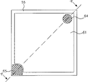
Fig. 1 is the plane graph that the LED of the single luminescence unit that has subsidiary electrode structure according to an embodiment of the invention is described, and Fig. 2 is the sectional view along the line A-A intercepting of Fig. 1.Short of additional description content, in the LED that describes Fig. 1 and single luminescence unit according to the embodiment of the invention illustrated in fig. 2 with subsidiary electrode structure employed technical pattern and feature be used for adaptively with Fig. 3 to relevant following each embodiment of Fig. 9.
Referring to Fig. 1 and Fig. 2, have the first conduction lower semiconductor layer 55, active layer 57 and the second conduction upper semiconductor layer 59 according to the LED 1a of the single luminescence unit with subsidiary electrode structure of the embodiment of the invention, described layer is formed on the substrate 51.Following graphic in, under the situation that does not break away from essence spirit of the present invention, LED 1a will illustrate adaptively and be luminescence unit 1.
Simultaneously, lower and upper semiconductor layer 55 and 59 is formed by band gap (band gap) specific activity layer 57 big material, and can be formed by the compound semiconductor based on GaN.For instance, the second conductive compound semiconductor layer of formation lower semiconductor layer 55 can comprise Al
xGa
1-xN (0≤x<1).
Simultaneously, resilient coating 53 can be between lower semiconductor layer 55 and substrate 51.Use resilient coating 53 reduces the mismatch (mismatch) between substrate 51 and the lower semiconductor layer 55.
As shown in Figure 2, upper semiconductor layer 59 is positioned on the subregion of lower semiconductor layer 55, and active layer 57 is between upper semiconductor layer 59 and lower semiconductor layer 55.In addition, upper electrode layer 61 can be positioned on the upper semiconductor layer 59.Can (for example) form as the upper electrode layer 61 of transparent electrode layer by the material of for example tin indium oxide (ITO) or Ni/Au.
Simultaneously, bottom electrode 65 is positioned on the lower semiconductor layer 55 and locates to expose in first corner (corner, lower-left of Fig. 1) of substrate 51.Upper electrode layer 61 is formed on the upper semiconductor layer 59, and top electrode pole plate 64 is positioned on the upper electrode layer 61 and second corner (the upper right corner of Fig. 1) that is positioned at substrate 51 is located.Can use (lift off) technology of peeling off, form top electrode pole plate 64 by at least one that is selected from Ni, Cr, Pd, Pt, W and Al.Top electrode pole plate 64 can comprise at least one layer or alloy-layer.
When lower semiconductor layer 55 is the N type, can use lift-off technology, form bottom electrode 65 by Ti/Al.In addition, bottom electrode 65 can be formed by at least one that is selected from Ni, Cr, Pd, Pt, W and Al, and can comprise at least one layer or alloy-layer.
Upper electrode layer 61 (it is a transparent electrode layer) is formed having the transparency by (for example) ITO or Ni/Au, and forms ohmic contact with upper semiconductor layer 59, to reduce contact resistance.Yet top electrode pole plate 64 does not have the transparency, and does not form ohmic contact with upper semiconductor layer 59.Because upper electrode layer 61 is formed between top electrode pole plate and the upper semiconductor layer 59, thus current concentration might be prevented below top electrode pole plate 64, and prevent that light from being absorbed by top electrode pole plate 64 and lose.
In addition, form the top electrode pole plate 64 that has relatively than small size, thereby improve the CURRENT DISTRIBUTION in the upper semiconductor layer 59 at the corner of upper semiconductor layer 59.
In addition, top electrode pole plate 64 and bottom electrode 65 are placed in the corner respect to one another of substrate 51 respectively.Therefore, the electric current of supplying by top electrode pole plate 64 can be evenly distributed in the upper electrode layer 61.
Fig. 3 is the schematic diagram of explanation according to the LED of the serial array with the luminescence unit shown in Fig. 1 of the embodiment of the invention.Described serial array is placed in the one chip 50.
Referring to Fig. 3, one chip 50 has substrate 51.Substrate 51 can be the conductive substrates that is formed with insulating barrier on dielectric substrate or the upper surface.A plurality of luminescence units 1 are placed on the substrate 51.Luminescence unit is by the lead connection that is one another in series, to form serial array 52.Joint sheet 71 can be positioned on the place, two ends of serial array 52.Joint sheet 71 is electrically connected to the two ends of serial array 52 respectively.
In an embodiment of the present invention, the luminescence unit in the one chip 50 can all be connected in series on the single substrate.Therefore, luminescence unit 1 is formed on the single substrate with the technology of the lead that is formed for being connected luminescence unit 1 and simplifies.
Fig. 4 is the partial cross section figure of employed luminescence unit in the explanation embodiment of the invention, and wherein luminescence unit is connected in series by the lead that is formed by step covering process (step cover process).Yet luminescence unit can be connected in series by the lead that is formed by gas bridge (air bridge) technology and step covering process.
Referring to Fig. 3, a plurality of luminescence units 1 separate each other on substrate 51.In the luminescence unit 1 each comprises: lower semiconductor layer 55, and it is made up of the first conductive compound semiconductor layer; Active layer 57; With upper semiconductor layer 59, it is made up of the second conductive compound semiconductor layer.Active layer 57 can have the single or multiple quantum well structures that comprise trap layer and barrier layer, wherein selects the component of substrate and active layer 57 according to required light emission wavelength.For instance, active layer 57 can be formed by the compound semiconductor based on GaN.Lower and upper semiconductor layer 55 and 59 can be formed and be formed by the compound semiconductor based on GaN than these active layer 57 big materials by band gap.
Simultaneously, resilient coating 53 can be between lower semiconductor layer 55 and substrate 51.Use resilient coating 52 reduces the mismatch between substrate 51 and the lower semiconductor layer 55.As shown in Figure 4, resilient coating 53 can be through forming having the part that separates each other, but the invention is not restricted to this.If resilient coating 53 is formed by insulating material or material with big resistance, resilient coating 53 is formed on the substrate 51 serially so.
As shown in Figure 4, upper semiconductor layer 59 is positioned on the subregion of lower semiconductor layer 55, and active layer 57 is between upper semiconductor layer 59 and lower semiconductor layer 55.In addition, upper electrode layer 61 can be positioned on the upper semiconductor layer 59.Can (for example) form as the upper electrode layer 61 of transparent electrode layer by the material of for example tin indium oxide (ITO) or Ni/Au.
Simultaneously, luminescence unit 1 is reached electrical connection by lead 87.The lower semiconductor layer 55 of one in the described luminescence unit is connected to the upper electrode layer 61 of another the adjacent person in the described luminescence unit by lead 87.As shown in Figure 4, the top electrode pole plate 64 that is formed on the upper electrode layer 61 can be connected respectively to bottom electrode 65 on the exposed region that is formed at lower semiconductor layer 55 by lead 87.
Can be formed for connecting the lead 87 of luminescence unit 1 by the step covering process.That is, cover all layer and substrates 51 of luminescence unit 1, be used to contact except the part of this lead 87 with insulating barrier 85.Then, lead 87 is patterned on insulating barrier 85, makes luminescence unit 1 be electrically connected to each other.
For instance, insulating barrier 85 has the opening that is used to make top electrode pole plate 64 and bottom electrode 65 exposures.Lead 87 connects the top electrode pole plate 64 and the bottom electrode 65 of luminescence unit adjacent one another are by described opening, and luminescence unit is connected in series.Therefore, formed serial array 52 (see figure 3)s, wherein luminescence unit is connected in series on the single substrate 51 by lead 87.
As described above, described and used a kind of AC LED that on substrate, has the one chip of serial array.Yet, can use one chip to dispose the AC light-emitting device, each in the described one chip has reverse parallel connection and is connected serial array on the substrate.
Fig. 5 is that explanation is used and to be had the schematic diagram of AC LED that reverse parallel connection is connected the one chip 100 of the serial array on the single substrate.
Referring to Fig. 5, two serial array 52a and 52c are placed on the substrate 51, and each among two serial array 52a and the 52c all has the luminescence unit 1 that is connected in series. Serial array 52a and 52c reverse parallel connection each other are connected between joint sheet 71a and the 71b.
When this type of one chip 100 is one another in series connection by a kind of connecting elements (not shown), can form at least two array group.Described connecting elements can be the closing line that is used for directly connecting joint sheet.That is, one chip is installed in the corresponding encapsulation, and the one chip that is installed in the corresponding encapsulation is connected to each other by closing line, thereby forms some array group.Perhaps, as indicated above, one chip 100 is installed in the corresponding encapsulation, and encapsulation is connected in series accordingly, thereby forms some array group.In addition, can use one chip and encapsulation to form differently the serial array group.
Simultaneously, be formed at corresponding serial array 52a on the same substrate 51 and the corresponding luminescence unit 1 among the 52c and reach electrical connection by connecting elements 105.Promptly, among two the serial array 52a and 52c that connects at reverse parallel connection each other, be positioned at least one luminescence unit in any one of serial array is electrically connected to another person who is arranged in serial array by connecting elements 105 at least one corresponding luminescence unit.Connecting elements 105 prevents that overvoltage is applied to the luminescence unit in the serial array that is applied in reverse voltage.Connecting elements 105 can connect the first conduction lower semiconductor layer, and described first conduction each in the lower semiconductor layer is used jointly by the adjacent luminescence unit of the luminescence unit 1 in each of serial array 52a and 52c.Perhaps, connecting elements 105 can connect many leads, its through forming so that the adjacent luminescence unit in the luminescence unit 1 among corresponding serial array 52a and the 52c is one another in series is connected.
According to this embodiment, some one chips 100 are connected in series to form some array group, thereby reduce the number of the luminescence unit in the serial array on the single substrate, in in described some one chips 100 each, each serial array 52a with the luminescence unit that is connected in series and 52c reverse parallel connection each other are being connected.
Fig. 6 illustrates the photo of the electrode structure of LED according to an embodiment of the invention.
Referring to Fig. 6, plurality of luminescence units is placed in the array on the substrate.Corresponding luminescence unit is electrically connected to each other by the connecting elements that is formed by the step covering process.
Can find out that the top electrode pole plate and the bottom electrode that are provided in each luminescence unit are placed in corner respect to one another respectively.The percentage of the area that is taken by top electrode pole plate and bottom electrode in each luminescence unit is relative less.In addition, the configuration of this type of in of luminescence unit is with respect to another adjacent person of luminescence unit and symmetrical placement.That is, top electrode pole plate in each luminescence unit and bottom electrode are placed in the corner on the diagonal respectively.One top electrode pole plate of luminescence unit and bottom electrode are through arranging with respect to another adjacent person's of luminescence unit top electrode pole plate and bottom electrode and symmetry.
Because the top electrode pole plate and the bottom electrode that are provided in each luminescence unit are placed in corner respect to one another respectively, so corresponding luminescence unit can be through settling, so that when two luminescence units in the luminescence unit were electrically connected to each other, the length of connecting elements minimized.
For instance, first, second is arranged on the line with the 3rd luminescence unit 1,2 and 3.At this moment, first luminescence unit 1 has bottom electrode that is placed in the lower-left corner and the top electrode pole plate that is placed in upper right corner.In addition, second luminescence unit 2 has bottom electrode that is placed in upper left corner and the top electrode pole plate that is placed in the bottom right corner.In addition, the 3rd luminescence unit 3 has bottom electrode that is placed in the lower-left corner and the top electrode pole plate that is placed in upper right corner.
In addition, the 4th luminescence unit 4 has top electrode pole plate that is placed in upper left corner and the bottom electrode that is placed in the bottom right corner.Third and fourth luminescence unit 3 and 4 is connected to each other by connecting elements.
As indicated above, in each luminescence unit, top electrode pole plate and bottom electrode are placed in corner respect to one another respectively, thereby when making AC LED, have simplified technology, and improved reliability.
In addition, in each luminescence unit, the size that is placed in the top electrode pole plate of corner respect to one another and bottom electrode respectively is less, the light that top electrode pole plate and bottom electrode is stopped send from LED regional less, and the luminous zone is bigger.
Fig. 7 illustrates the photo of electrode structure of a kind of LED of the Comparative Example that will compare with the electrode structure of the LED of the embodiment of the invention.
Referring to Fig. 7, top electrode pole plate and bottom electrode extend through forming to be placed in according to the edge of two opposite sides in each luminescence unit among the LED of Comparative Example respectively.As can be seen, the percentage of the area that is taken by top electrode pole plate and bottom electrode in each luminescence unit is significantly greater than the situation of Fig. 6.Therefore, as can be seen, because the area that is taken by top electrode pole plate, bottom electrode and lead is wider, so reduce the luminous zone.
Fig. 8 is the chart that illustrates according to the luminous efficiency of the LED of the embodiment of the invention, and Fig. 9 is the chart that illustrates according to the luminous efficiency of the LED of Comparative Example.
That is, the optical power according to each the luminescence unit output that is provided from the LED shown in Fig. 6 of the embodiment of the invention is provided Fig. 8, wherein illustrates the luminescence unit number at each optical power value.
Optical power according to each the luminescence unit output that is provided from the LED shown in Fig. 7 of Comparative Example is provided Fig. 9, wherein illustrates the luminescence unit number at each optical power value.At this moment, the luminescence unit shown in Fig. 6 and Fig. 7 has same size.
Referring to Fig. 8, the optical power of each luminescence unit that is provided among the LED according to the embodiment of the invention is measured as average 135mW.Referring to Fig. 9, the optical power of each luminescence unit that is provided among the LED according to Comparative Example is measured as average 119mW.
By above-mentioned comparative result, can find out that luminous efficiency according to the LED of the embodiment of the invention is better than the luminous efficiency according to the LED of Comparative Example.
According to the present invention, be designed to lessly by top electrode pole plate and bottom electrode region occupied, make top electrode pole plate and bottom electrode stop and reduce, and the luminous zone is bigger, thereby improve luminous efficiency from the zone of the light of LED emission.
In addition, top electrode pole plate and bottom electrode among the LED are placed in corner respect to one another respectively, thereby make the CURRENT DISTRIBUTION maximization.
In addition, even when luminescence unit is electrically connected, the top electrode pole plate of each luminescence unit and bottom electrode also are placed in corner respectively, so that operation A C LED stably.Like this, a kind of connecting circuit can be configured to have the shortest path between adjacent another person's of one top electrode pole plate of luminescence unit and luminescence unit bottom electrode, thereby has simplified the manufacturing process of AC LED, and has improved reliability.
The present invention mentioned above is defined by aforementioned embodiment, but the those skilled in the art can do various modifications and change to it, and is included in the spirit and scope of the present invention that defined by appended claims.
For instance, Fig. 3 has described the various structures of the serial array with the luminescence unit that is connected in series in Fig. 5.Yet although not shown among the corresponding figure, each luminescence unit 1 that is comprised in each serial array has the electrode structure of describing in detail to Fig. 9 in conjunction with Fig. 6.Promptly, the top electrode pole plate and the bottom electrode that are formed in each luminescence unit 1 are placed in corner respect to one another on the diagonal respectively, and corresponding luminescence unit 1 through arranging so that luminescence unit one in the top electrode pole plate and bottom electrode with respect to the top electrode pole plate among another adjacent person of luminescence unit and bottom electrode and symmetry.The advantage of this type of electrode structure has been described to Fig. 9 in conjunction with Fig. 6 comprehensively.
Claims (16)
1. AC light-emitting diode, it comprises:
Substrate; And
At least one serial array, it has a plurality of luminescence units that are connected in series on the described substrate,
Each of wherein said luminescence unit comprises: lower semiconductor layer, and it is made up of the first conductive compound semiconductor layer on the top that is formed at described substrate; Upper semiconductor layer, it is made up of the second conductive compound semiconductor layer that is formed on the described lower semiconductor layer top; Active layer, it is between described lower semiconductor layer and upper semiconductor layer; Bottom electrode, it is formed on the described lower semiconductor layer and exposes at first corner of described substrate; Upper electrode layer, it is formed on the described upper semiconductor layer; And the top electrode pole plate, it is formed on the described upper electrode layer and exposes at second corner of described substrate,
Wherein said top electrode pole plate and described bottom electrode are placed in corner respect to one another on the diagonal of described luminescence unit respectively, and
Corresponding luminescence unit through arranging so that one described top electrode pole plate of described luminescence unit and described bottom electrode and and another person's of described one adjacent described luminescence units of described luminescence unit top electrode pole plate and the pass between the bottom electrode be reflective symmetry.
2. AC light-emitting diode according to claim 1 is characterized in that, described serial array comprises two serial array of reverse parallel connection connection each other.
3. AC light-emitting diode according to claim 1, it is characterized in that, described serial array comprises two serial array, wherein, described two serial array reverse parallel connection each other connect, and are positioned in any one of described serial array at least one in the described luminescence unit and are electrically connected to the correspondence that is positioned in the described luminescence unit in another serial array.
4. AC light-emitting diode according to claim 1 is characterized in that described upper electrode layer is a transparent electrode layer.
5. AC light-emitting diode according to claim 4 is characterized in that, described transparent electrode layer is formed by tin indium oxide (ITO).
6. AC light-emitting diode according to claim 1 is characterized in that, described top electrode pole plate is formed by at least one that is selected from Ni, Cr, Pd, Pt, W and Al.
7. AC light-emitting diode according to claim 6 is characterized in that, described top electrode pole plate comprises at least one layer or alloy-layer.
8. AC light-emitting diode according to claim 1 is characterized in that, described bottom electrode is formed by at least one that is selected from Ni, Cr, Pd, Pt, W and Al.
9. AC light-emitting diode according to claim 8 is characterized in that, described bottom electrode comprises at least one layer or alloy-layer.
10. AC light-emitting diode according to claim 1 is characterized in that, described active layer comprises and has In
xGa
1-xN trap layer and In
xGa
1-xThe single quantum well of N barrier layer or a plurality of quantum well structure are at In
xGa
1-xAmong the N, 0<x<1 is at In
xGa
1-xAmong the N, 0≤x<1.
11. AC light-emitting diode according to claim 10 is characterized in that, described In
xGa
1-xThe In content of N trap layer is more than described In
xGa
1-xThe In content of N barrier layer is at In
xGa
1-xAmong the N, 0<x<1 is at In
xGa
1-xAmong the N, 0≤x<1.
12. AC light-emitting diode according to claim 1 is characterized in that, the described second conductive compound semiconductor layer comprises Al
xGa
1-xN, wherein, 0≤x<1.
13. an AC light-emitting diode, it comprises:
The one chip that two or more are electrically connected in series,
Each of wherein said one chip comprises:
Substrate; And
At least one serial array, it has a plurality of luminescence units that are connected in series on the described substrate,
Each of wherein said luminescence unit comprises: lower semiconductor layer, and it is made up of the first conductive compound semiconductor layer on the top that is formed at described substrate; Upper semiconductor layer, it is made up of the second conductive compound semiconductor layer that is formed on the described lower semiconductor layer top; Active layer, it is between described lower semiconductor layer and upper semiconductor layer; Bottom electrode, it is formed on the described lower semiconductor layer and exposes at first corner of described substrate; Upper electrode layer, it is formed on the described upper semiconductor layer; And the top electrode pole plate, it is formed on the described upper electrode layer and exposes at second corner of described substrate,
Wherein said top electrode pole plate and described bottom electrode are placed in corner respect to one another on the diagonal of described luminescence unit respectively, and
Corresponding luminescence unit through arranging so that one described top electrode pole plate of described luminescence unit and described bottom electrode and and another person's of described one adjacent described luminescence units of described luminescence unit top electrode pole plate and the pass between the bottom electrode be reflective symmetry.
14. AC light-emitting diode according to claim 13 is characterized in that, described serial array comprises two serial array of reverse parallel connection connection each other.
15. AC light-emitting diode according to claim 13 is characterized in that, described two or more one chips are installed in the corresponding encapsulation and by closing line and are connected in series.
16. AC light-emitting diode according to claim 13 is characterized in that, described two or more one chips are installed in the corresponding encapsulation, and described encapsulation is being connected in series.
Applications Claiming Priority (2)
| Application Number | Priority Date | Filing Date | Title |
|---|---|---|---|
| KR1020070026697A KR100974923B1 (en) | 2007-03-19 | 2007-03-19 | Light emitting diode |
| KR10-2007-0026697 | 2007-03-19 |
Related Child Applications (1)
| Application Number | Title | Priority Date | Filing Date |
|---|---|---|---|
| CN201010110113.9A Division CN101958334B (en) | 2007-03-19 | 2008-03-18 | Light emitting diode |
Publications (2)
| Publication Number | Publication Date |
|---|---|
| CN101271915A CN101271915A (en) | 2008-09-24 |
| CN101271915B true CN101271915B (en) | 2011-05-04 |
Family
ID=39529671
Family Applications (2)
| Application Number | Title | Priority Date | Filing Date |
|---|---|---|---|
| CN201010110113.9A Expired - Fee Related CN101958334B (en) | 2007-03-19 | 2008-03-18 | Light emitting diode |
| CN2008100840155A Expired - Fee Related CN101271915B (en) | 2007-03-19 | 2008-03-18 | Light emitting diode |
Family Applications Before (1)
| Application Number | Title | Priority Date | Filing Date |
|---|---|---|---|
| CN201010110113.9A Expired - Fee Related CN101958334B (en) | 2007-03-19 | 2008-03-18 | Light emitting diode |
Country Status (5)
| Country | Link |
|---|---|
| US (3) | US8896011B2 (en) |
| EP (1) | EP1973161A3 (en) |
| JP (2) | JP5490997B2 (en) |
| KR (1) | KR100974923B1 (en) |
| CN (2) | CN101958334B (en) |
Families Citing this family (106)
| Publication number | Priority date | Publication date | Assignee | Title |
|---|---|---|---|---|
| JP3802910B2 (en) * | 2004-09-13 | 2006-08-02 | ローム株式会社 | Semiconductor light emitting device |
| KR100631898B1 (en) * | 2005-01-19 | 2006-10-11 | 삼성전기주식회사 | Gallium nitride based light emitting device having ESD protection capability and method for manufacturing same |
| US8476648B2 (en) | 2005-06-22 | 2013-07-02 | Seoul Opto Device Co., Ltd. | Light emitting device and method of manufacturing the same |
| US7998761B2 (en) | 2006-01-09 | 2011-08-16 | Seoul Opto Device Co., Ltd. | Light emitting diode with ITO layer and method for fabricating the same |
| WO2009125953A2 (en) * | 2008-04-06 | 2009-10-15 | Song June O | Luminous element |
| US8871024B2 (en) | 2008-06-05 | 2014-10-28 | Soraa, Inc. | High pressure apparatus and method for nitride crystal growth |
| US9157167B1 (en) | 2008-06-05 | 2015-10-13 | Soraa, Inc. | High pressure apparatus and method for nitride crystal growth |
| US8097081B2 (en) | 2008-06-05 | 2012-01-17 | Soraa, Inc. | High pressure apparatus and method for nitride crystal growth |
| TWI464921B (en) | 2009-02-25 | 2014-12-11 | Epistar Corp | Light-emitting device with narrow dominant wavelength distribution and method of making the same |
| US8979999B2 (en) | 2008-08-07 | 2015-03-17 | Soraa, Inc. | Process for large-scale ammonothermal manufacturing of gallium nitride boules |
| US8430958B2 (en) | 2008-08-07 | 2013-04-30 | Soraa, Inc. | Apparatus and method for seed crystal utilization in large-scale manufacturing of gallium nitride |
| US10036099B2 (en) | 2008-08-07 | 2018-07-31 | Slt Technologies, Inc. | Process for large-scale ammonothermal manufacturing of gallium nitride boules |
| US8021481B2 (en) | 2008-08-07 | 2011-09-20 | Soraa, Inc. | Process and apparatus for large-scale manufacturing of bulk monocrystalline gallium-containing nitride |
| US7976630B2 (en) | 2008-09-11 | 2011-07-12 | Soraa, Inc. | Large-area seed for ammonothermal growth of bulk gallium nitride and method of manufacture |
| US7939839B2 (en) * | 2008-09-11 | 2011-05-10 | Bridgelux, Inc. | Series connected segmented LED |
| US8354679B1 (en) | 2008-10-02 | 2013-01-15 | Soraa, Inc. | Microcavity light emitting diode method of manufacture |
| US8455894B1 (en) | 2008-10-17 | 2013-06-04 | Soraa, Inc. | Photonic-crystal light emitting diode and method of manufacture |
| KR100999689B1 (en) * | 2008-10-17 | 2010-12-08 | 엘지이노텍 주식회사 | Semiconductor light emitting device and fabrication method thereof, light emitting apparatus having the same |
| US9543392B1 (en) | 2008-12-12 | 2017-01-10 | Soraa, Inc. | Transparent group III metal nitride and method of manufacture |
| US8878230B2 (en) | 2010-03-11 | 2014-11-04 | Soraa, Inc. | Semi-insulating group III metal nitride and method of manufacture |
| US8461071B2 (en) | 2008-12-12 | 2013-06-11 | Soraa, Inc. | Polycrystalline group III metal nitride with getter and method of making |
| US8987156B2 (en) | 2008-12-12 | 2015-03-24 | Soraa, Inc. | Polycrystalline group III metal nitride with getter and method of making |
| USRE47114E1 (en) | 2008-12-12 | 2018-11-06 | Slt Technologies, Inc. | Polycrystalline group III metal nitride with getter and method of making |
| KR20100076083A (en) | 2008-12-17 | 2010-07-06 | 서울반도체 주식회사 | Light emitting diode having plurality of light emitting cells and method of fabricating the same |
| KR101533817B1 (en) * | 2008-12-31 | 2015-07-09 | 서울바이오시스 주식회사 | Light emitting device having plurality of non-polar light emitting cells and method of fabricating the same |
| KR100972980B1 (en) | 2009-02-25 | 2010-07-29 | 삼성엘이디 주식회사 | Semiconductor light emitting device and manufacturing method thereof |
| US7982409B2 (en) | 2009-02-26 | 2011-07-19 | Bridgelux, Inc. | Light sources utilizing segmented LEDs to compensate for manufacturing variations in the light output of individual segmented LEDs |
| JP4801751B2 (en) * | 2009-02-27 | 2011-10-26 | シャープ株式会社 | LED module and LED light source device |
| US8247886B1 (en) | 2009-03-09 | 2012-08-21 | Soraa, Inc. | Polarization direction of optical devices using selected spatial configurations |
| US8299473B1 (en) | 2009-04-07 | 2012-10-30 | Soraa, Inc. | Polarized white light devices using non-polar or semipolar gallium containing materials and transparent phosphors |
| US8791499B1 (en) | 2009-05-27 | 2014-07-29 | Soraa, Inc. | GaN containing optical devices and method with ESD stability |
| US8558249B1 (en) | 2009-06-30 | 2013-10-15 | Applied Lighting Solutions, LLC | Rectifier structures for AC LED systems |
| FR2949278B1 (en) * | 2009-08-18 | 2012-11-02 | Commissariat Energie Atomique | METHOD FOR MANUFACTURING A LIGHT EMITTING DEVICE BASED ON LIGHT EMITTING DIODES |
| US9000466B1 (en) | 2010-08-23 | 2015-04-07 | Soraa, Inc. | Methods and devices for light extraction from a group III-nitride volumetric LED using surface and sidewall roughening |
| US8933644B2 (en) | 2009-09-18 | 2015-01-13 | Soraa, Inc. | LED lamps with improved quality of light |
| CN102630349B (en) | 2009-09-18 | 2017-06-13 | 天空公司 | Method power led and using current density operation |
| US9583678B2 (en) | 2009-09-18 | 2017-02-28 | Soraa, Inc. | High-performance LED fabrication |
| US9293644B2 (en) | 2009-09-18 | 2016-03-22 | Soraa, Inc. | Power light emitting diode and method with uniform current density operation |
| US8435347B2 (en) | 2009-09-29 | 2013-05-07 | Soraa, Inc. | High pressure apparatus with stackable rings |
| US9175418B2 (en) | 2009-10-09 | 2015-11-03 | Soraa, Inc. | Method for synthesis of high quality large area bulk gallium based crystals |
| US9324691B2 (en) * | 2009-10-20 | 2016-04-26 | Epistar Corporation | Optoelectronic device |
| TWI533474B (en) * | 2009-10-20 | 2016-05-11 | 晶元光電股份有限公司 | Optoelectronic device |
| US8740413B1 (en) | 2010-02-03 | 2014-06-03 | Soraa, Inc. | System and method for providing color light sources in proximity to predetermined wavelength conversion structures |
| US8905588B2 (en) | 2010-02-03 | 2014-12-09 | Sorra, Inc. | System and method for providing color light sources in proximity to predetermined wavelength conversion structures |
| US10147850B1 (en) | 2010-02-03 | 2018-12-04 | Soraa, Inc. | System and method for providing color light sources in proximity to predetermined wavelength conversion structures |
| US8084775B2 (en) * | 2010-03-16 | 2011-12-27 | Bridgelux, Inc. | Light sources with serially connected LED segments including current blocking diodes |
| TWI450415B (en) * | 2010-03-23 | 2014-08-21 | Lg Innotek Co Ltd | Light emitting device, light emitting device package and lighting system |
| US9450143B2 (en) | 2010-06-18 | 2016-09-20 | Soraa, Inc. | Gallium and nitrogen containing triangular or diamond-shaped configuration for optical devices |
| US9564320B2 (en) | 2010-06-18 | 2017-02-07 | Soraa, Inc. | Large area nitride crystal and method for making it |
| US20120007102A1 (en) * | 2010-07-08 | 2012-01-12 | Soraa, Inc. | High Voltage Device and Method for Optical Devices |
| TWI557934B (en) * | 2010-09-06 | 2016-11-11 | 晶元光電股份有限公司 | A semiconductor optoelectronic device |
| FR2975532B1 (en) * | 2011-05-18 | 2013-05-10 | Commissariat Energie Atomique | ELECTRICAL CONNECTION IN SERIES OF LIGHT EMITTING NANOWIRES |
| US9070851B2 (en) | 2010-09-24 | 2015-06-30 | Seoul Semiconductor Co., Ltd. | Wafer-level light emitting diode package and method of fabricating the same |
| CN102446948B (en) * | 2010-10-12 | 2014-07-30 | 晶元光电股份有限公司 | Light emitting element |
| US8729559B2 (en) | 2010-10-13 | 2014-05-20 | Soraa, Inc. | Method of making bulk InGaN substrates and devices thereon |
| CN102479902B (en) * | 2010-11-23 | 2017-04-12 | 晶元光电股份有限公司 | Light emitting assembly |
| US8786053B2 (en) | 2011-01-24 | 2014-07-22 | Soraa, Inc. | Gallium-nitride-on-handle substrate materials and devices and method of manufacture |
| KR20120092000A (en) | 2011-02-09 | 2012-08-20 | 서울반도체 주식회사 | Light emitting device having wavelength converting layer |
| US8492185B1 (en) | 2011-07-14 | 2013-07-23 | Soraa, Inc. | Large area nonpolar or semipolar gallium and nitrogen containing substrate and resulting devices |
| US8686431B2 (en) | 2011-08-22 | 2014-04-01 | Soraa, Inc. | Gallium and nitrogen containing trilateral configuration for optical devices |
| US9694158B2 (en) | 2011-10-21 | 2017-07-04 | Ahmad Mohamad Slim | Torque for incrementally advancing a catheter during right heart catheterization |
| US10029955B1 (en) | 2011-10-24 | 2018-07-24 | Slt Technologies, Inc. | Capsule for high pressure, high temperature processing of materials and methods of use |
| KR101888604B1 (en) * | 2011-10-28 | 2018-08-14 | 엘지이노텍 주식회사 | Light emitting device and light emitting device package |
| KR101871372B1 (en) * | 2011-10-28 | 2018-08-02 | 엘지이노텍 주식회사 | Light emitting device |
| US8912025B2 (en) | 2011-11-23 | 2014-12-16 | Soraa, Inc. | Method for manufacture of bright GaN LEDs using a selective removal process |
| US8482104B2 (en) | 2012-01-09 | 2013-07-09 | Soraa, Inc. | Method for growth of indium-containing nitride films |
| JP2013165188A (en) * | 2012-02-10 | 2013-08-22 | Oki Data Corp | Semiconductor light-emitting device, light source device, image forming apparatus and image display device |
| EP2626901A1 (en) | 2012-02-10 | 2013-08-14 | Oki Data Corporation | Semiconductor light emitting apparatus, image displaying apparatus, mobile terminal, head-up display apparatus, image projector, head-mounted display apparatus, and image forming apparatus |
| US9269876B2 (en) | 2012-03-06 | 2016-02-23 | Soraa, Inc. | Light emitting diodes with low refractive index material layers to reduce light guiding effects |
| TWI549278B (en) * | 2012-03-12 | 2016-09-11 | 晶元光電股份有限公司 | Light-emitting diode device |
| CN103367610A (en) * | 2012-03-29 | 2013-10-23 | 比亚迪股份有限公司 | High-voltage LED chip and production method thereof |
| US10388690B2 (en) | 2012-08-07 | 2019-08-20 | Seoul Viosys Co., Ltd. | Wafer level light-emitting diode array |
| US8971368B1 (en) | 2012-08-16 | 2015-03-03 | Soraa Laser Diode, Inc. | Laser devices having a gallium and nitrogen containing semipolar surface orientation |
| CN102820316B (en) * | 2012-08-30 | 2016-04-27 | 北京工业大学 | A kind of LED display microarray and preparation method thereof |
| DE202013012470U1 (en) * | 2012-09-07 | 2017-01-12 | Seoul Viosys Co., Ltd. | Light-emitting diode array on WAFER level |
| US9978904B2 (en) | 2012-10-16 | 2018-05-22 | Soraa, Inc. | Indium gallium nitride light emitting devices |
| CN103840054A (en) * | 2012-11-20 | 2014-06-04 | 展晶科技(深圳)有限公司 | Light-emitting-diode chip |
| US9356212B2 (en) | 2012-12-21 | 2016-05-31 | Seoul Viosys Co., Ltd. | Light emitting diode and method of fabricating the same |
| US8802471B1 (en) | 2012-12-21 | 2014-08-12 | Soraa, Inc. | Contacts for an n-type gallium and nitrogen substrate for optical devices |
| CN107768399B (en) * | 2012-12-21 | 2022-02-18 | 首尔伟傲世有限公司 | Light emitting diode |
| JP6176032B2 (en) * | 2013-01-30 | 2017-08-09 | 日亜化学工業株式会社 | Semiconductor light emitting device |
| TW201438188A (en) * | 2013-03-25 | 2014-10-01 | Miracle Technology Co Ltd | Stacked LED array structure |
| US8994033B2 (en) | 2013-07-09 | 2015-03-31 | Soraa, Inc. | Contacts for an n-type gallium and nitrogen substrate for optical devices |
| EP2830094B1 (en) | 2013-07-22 | 2020-02-26 | LG Innotek Co., Ltd. | Light emitting device |
| JP6264568B2 (en) * | 2013-08-06 | 2018-01-24 | パナソニックIpマネジメント株式会社 | Light emitting device and display device |
| US9419189B1 (en) | 2013-11-04 | 2016-08-16 | Soraa, Inc. | Small LED source with high brightness and high efficiency |
| KR102162437B1 (en) | 2014-05-15 | 2020-10-07 | 엘지이노텍 주식회사 | Light emitting device and light emitting device package including the device |
| FR3023061B1 (en) * | 2014-06-27 | 2017-12-15 | Commissariat Energie Atomique | MESA STRUCTURE DIODE WITH SUBSTANTIALLY PLANE CONTACT SURFACE |
| CN104362236B (en) * | 2014-11-11 | 2017-03-08 | 杭州士兰明芯科技有限公司 | A kind of LED structure and preparation method thereof |
| CN104538417B (en) * | 2015-01-08 | 2017-11-03 | 电子科技大学 | LED open-circuit-protections integrated chip and its manufacture method based on diode chain |
| JP5967269B2 (en) * | 2015-06-11 | 2016-08-10 | 日亜化学工業株式会社 | Light emitting device |
| CN107924658B (en) * | 2015-08-20 | 2020-09-25 | 三菱电机株式会社 | LED display device and driving device |
| CN205944139U (en) | 2016-03-30 | 2017-02-08 | 首尔伟傲世有限公司 | Ultraviolet ray light -emitting diode spare and contain this emitting diode module |
| DE102016112587A1 (en) * | 2016-07-08 | 2018-01-11 | Osram Opto Semiconductors Gmbh | Radiation-emitting semiconductor chip |
| US10174438B2 (en) | 2017-03-30 | 2019-01-08 | Slt Technologies, Inc. | Apparatus for high pressure reaction |
| KR20180124224A (en) * | 2017-05-11 | 2018-11-21 | 서울바이오시스 주식회사 | Light emitting diode with zinc oxide layer |
| KR102450579B1 (en) * | 2017-06-05 | 2022-10-07 | 삼성전자주식회사 | Led lamp |
| KR102549171B1 (en) | 2017-07-12 | 2023-06-30 | 삼성전자주식회사 | Led lighting device package and display apparatus using the same |
| US11749790B2 (en) * | 2017-12-20 | 2023-09-05 | Lumileds Llc | Segmented LED with embedded transistors |
| US11355549B2 (en) | 2017-12-29 | 2022-06-07 | Lumileds Llc | High density interconnect for segmented LEDs |
| KR20200095210A (en) * | 2019-01-31 | 2020-08-10 | 엘지전자 주식회사 | Semiconductor light emitting device, manufacturing method thereof, and display device including the same |
| KR20210105258A (en) * | 2020-02-18 | 2021-08-26 | 주식회사 루멘스 | LED lighting apparatuses for display |
| US20230246411A1 (en) * | 2020-07-20 | 2023-08-03 | Sony Semiconductor Solutions Corporation | Light emitting device |
| CN113140966B (en) * | 2021-03-09 | 2023-05-09 | 深圳瑞波光电子有限公司 | Semiconductor laser bar, manufacturing method thereof and electronic equipment |
| CN114068775B (en) * | 2021-10-18 | 2023-08-15 | 厦门三安光电有限公司 | Flip LED chip, LED packaging module and display device |
| CN114857511B (en) | 2022-04-11 | 2024-02-20 | 厦门普为光电科技有限公司 | Light emitting diode |
Citations (3)
| Publication number | Priority date | Publication date | Assignee | Title |
|---|---|---|---|---|
| CN1753199A (en) * | 2004-09-23 | 2006-03-29 | 璨圆光电股份有限公司 | Gallium nitride series luminous diode |
| CN1770447A (en) * | 2005-09-21 | 2006-05-10 | 杭州士兰明芯科技有限公司 | Light-emitting diode lamp using AC power supply and its manufacturing method |
| CN1913180A (en) * | 2005-08-11 | 2007-02-14 | 璨圆光电股份有限公司 | LEd component and its driving method |
Family Cites Families (22)
| Publication number | Priority date | Publication date | Assignee | Title |
|---|---|---|---|---|
| EP0952617B1 (en) * | 1993-04-28 | 2004-07-28 | Nichia Corporation | Gallium nitride-based III-V group compound semiconductor device |
| DE4324662A1 (en) * | 1993-07-22 | 1995-01-26 | Voith Gmbh J M | Sieve |
| JP3659098B2 (en) * | 1999-11-30 | 2005-06-15 | 日亜化学工業株式会社 | Nitride semiconductor light emitting device |
| DE10051159C2 (en) * | 2000-10-16 | 2002-09-19 | Osram Opto Semiconductors Gmbh | LED module, e.g. White light source |
| JP3822545B2 (en) * | 2002-04-12 | 2006-09-20 | 士郎 酒井 | Light emitting device |
| TWI249148B (en) | 2004-04-13 | 2006-02-11 | Epistar Corp | Light-emitting device array having binding layer |
| CN100595938C (en) * | 2002-08-01 | 2010-03-24 | 日亚化学工业株式会社 | Semiconductor light emitting device, manufacturing method thereof, and light emitting device using the same |
| EP1553641B1 (en) * | 2002-08-29 | 2011-03-02 | Seoul Semiconductor Co., Ltd. | Light-emitting device having light-emitting diodes |
| TWI223460B (en) * | 2003-09-23 | 2004-11-01 | United Epitaxy Co Ltd | Light emitting diodes in series connection and method of making the same |
| KR100571819B1 (en) * | 2003-10-16 | 2006-04-17 | 삼성전자주식회사 | light emitting device and method of manufacturing the same using p-type conductive transparent oxide thin film electrode |
| US7781777B2 (en) * | 2004-03-08 | 2010-08-24 | Showa Denko K.K. | Pn junction type group III nitride semiconductor light-emitting device |
| KR20060065954A (en) * | 2004-12-11 | 2006-06-15 | 서울옵토디바이스주식회사 | Luminous element having arrayed cells and method of manufacturing thereof |
| JP3904571B2 (en) | 2004-09-02 | 2007-04-11 | ローム株式会社 | Semiconductor light emitting device |
| JP3802911B2 (en) * | 2004-09-13 | 2006-08-02 | ローム株式会社 | Semiconductor light emitting device |
| US7566908B2 (en) * | 2004-11-29 | 2009-07-28 | Yongsheng Zhao | Gan-based and ZnO-based LED |
| KR101138944B1 (en) | 2005-01-26 | 2012-04-25 | 서울옵토디바이스주식회사 | Light emitting device having a plurality of light emitting cells connected in series and method of fabricating the same |
| US7525248B1 (en) * | 2005-01-26 | 2009-04-28 | Ac Led Lighting, L.L.C. | Light emitting diode lamp |
| TW200642101A (en) * | 2005-05-18 | 2006-12-01 | Univ Southern Taiwan Tech | Photodetector |
| JP4359263B2 (en) * | 2005-05-18 | 2009-11-04 | ローム株式会社 | Semiconductor light emitting device |
| KR100616415B1 (en) | 2005-08-08 | 2006-08-29 | 서울옵토디바이스주식회사 | Alternate current type light-emitting diode |
| TWI331406B (en) | 2005-12-14 | 2010-10-01 | Advanced Optoelectronic Tech | Single chip with multi-led |
| US7714348B2 (en) * | 2006-10-06 | 2010-05-11 | Ac-Led Lighting, L.L.C. | AC/DC light emitting diodes with integrated protection mechanism |
-
2007
- 2007-03-19 KR KR1020070026697A patent/KR100974923B1/en active IP Right Grant
-
2008
- 2008-03-07 EP EP08004224A patent/EP1973161A3/en not_active Ceased
- 2008-03-18 CN CN201010110113.9A patent/CN101958334B/en not_active Expired - Fee Related
- 2008-03-18 CN CN2008100840155A patent/CN101271915B/en not_active Expired - Fee Related
- 2008-03-18 US US12/050,873 patent/US8896011B2/en active Active
- 2008-03-19 JP JP2008070697A patent/JP5490997B2/en not_active Expired - Fee Related
-
2011
- 2011-05-19 US US13/111,406 patent/US8283682B2/en not_active Expired - Fee Related
-
2014
- 2014-02-27 JP JP2014037340A patent/JP5799124B2/en not_active Expired - Fee Related
- 2014-11-24 US US14/551,808 patent/US9461091B2/en active Active
Patent Citations (3)
| Publication number | Priority date | Publication date | Assignee | Title |
|---|---|---|---|---|
| CN1753199A (en) * | 2004-09-23 | 2006-03-29 | 璨圆光电股份有限公司 | Gallium nitride series luminous diode |
| CN1913180A (en) * | 2005-08-11 | 2007-02-14 | 璨圆光电股份有限公司 | LEd component and its driving method |
| CN1770447A (en) * | 2005-09-21 | 2006-05-10 | 杭州士兰明芯科技有限公司 | Light-emitting diode lamp using AC power supply and its manufacturing method |
Also Published As
| Publication number | Publication date |
|---|---|
| US20110215346A1 (en) | 2011-09-08 |
| JP5799124B2 (en) | 2015-10-21 |
| KR100974923B1 (en) | 2010-08-10 |
| US8283682B2 (en) | 2012-10-09 |
| CN101271915A (en) | 2008-09-24 |
| KR20080085343A (en) | 2008-09-24 |
| CN101958334B (en) | 2014-06-04 |
| EP1973161A2 (en) | 2008-09-24 |
| EP1973161A3 (en) | 2011-03-02 |
| JP2008235894A (en) | 2008-10-02 |
| US20080230765A1 (en) | 2008-09-25 |
| US8896011B2 (en) | 2014-11-25 |
| US20150076532A1 (en) | 2015-03-19 |
| JP5490997B2 (en) | 2014-05-14 |
| US9461091B2 (en) | 2016-10-04 |
| JP2014112721A (en) | 2014-06-19 |
| CN101958334A (en) | 2011-01-26 |
Similar Documents
| Publication | Publication Date | Title |
|---|---|---|
| CN101271915B (en) | Light emitting diode | |
| JP6880148B2 (en) | Backlight unit using multi-cell light emitting diode | |
| US8299477B2 (en) | Light emitting device and method for fabricating the same | |
| JP5706614B2 (en) | AC drive type light emitting device | |
| US8785958B2 (en) | Light emitting element | |
| JP6267245B2 (en) | Light emitting device, method for manufacturing light emitting device, light emitting device package, and illumination system | |
| JP2009260311A (en) | Light-emitting device | |
| CN108346726A (en) | Light-emitting diode | |
| KR101861721B1 (en) | Light emitting device | |
| CN101286541B (en) | Semi-conductor illuminating device having fold transparent electrode | |
| CN205645804U (en) | Emitting diode filament and have its emitting diode lamp | |
| CN103117332B (en) | Photoelectric cell | |
| CN105140369B (en) | Light emitting diode structure | |
| KR20100047795A (en) | Light emitting diode for ac operation | |
| KR20120124640A (en) | Light emitting diode | |
| CN113659052A (en) | Light emitting diode, light emitting module and display device | |
| CN102479795A (en) | Alternating-current light emitting diode module | |
| KR20110121178A (en) | Light emitting diode having a plurality of light emitting cells | |
| JP2008177376A (en) | Light-emitting device and its driving method | |
| KR20130009038A (en) | Light emitting device, method of fabricating the same and light emitting device package |
Legal Events
| Date | Code | Title | Description |
|---|---|---|---|
| C06 | Publication | ||
| PB01 | Publication | ||
| C10 | Entry into substantive examination | ||
| SE01 | Entry into force of request for substantive examination | ||
| C14 | Grant of patent or utility model | ||
| GR01 | Patent grant | ||
| C56 | Change in the name or address of the patentee |
Owner name: SEOUL WEIAOSHI CO., LTD. Free format text: FORMER NAME: SEOUL OPTO DEVICE CO., LTD. |
|
| CP03 | Change of name, title or address |
Address after: South Korea Gyeonggi Do Anshan City Patentee after: SEOUL VIOSYS Co.,Ltd. Address before: Gyeonggi Do Korea Ansan danwon Yuan Dong 727-5,1-36 Patentee before: SEOUL OPTO DEVICE Co.,Ltd. |
|
| CF01 | Termination of patent right due to non-payment of annual fee | ||
| CF01 | Termination of patent right due to non-payment of annual fee |
Granted publication date: 20110504 |