JP4801751B2 - LED module and LED light source device - Google Patents
LED module and LED light source device Download PDFInfo
- Publication number
- JP4801751B2 JP4801751B2 JP2009045120A JP2009045120A JP4801751B2 JP 4801751 B2 JP4801751 B2 JP 4801751B2 JP 2009045120 A JP2009045120 A JP 2009045120A JP 2009045120 A JP2009045120 A JP 2009045120A JP 4801751 B2 JP4801751 B2 JP 4801751B2
- Authority
- JP
- Japan
- Prior art keywords
- terminal
- insulating substrate
- led module
- wiring
- connection
- Prior art date
- Legal status (The legal status is an assumption and is not a legal conclusion. Google has not performed a legal analysis and makes no representation as to the accuracy of the status listed.)
- Expired - Fee Related
Links
Images


Classifications
-
- G—PHYSICS
- G02—OPTICS
- G02F—OPTICAL DEVICES OR ARRANGEMENTS FOR THE CONTROL OF LIGHT BY MODIFICATION OF THE OPTICAL PROPERTIES OF THE MEDIA OF THE ELEMENTS INVOLVED THEREIN; NON-LINEAR OPTICS; FREQUENCY-CHANGING OF LIGHT; OPTICAL LOGIC ELEMENTS; OPTICAL ANALOGUE/DIGITAL CONVERTERS
- G02F1/00—Devices or arrangements for the control of the intensity, colour, phase, polarisation or direction of light arriving from an independent light source, e.g. switching, gating or modulating; Non-linear optics
- G02F1/01—Devices or arrangements for the control of the intensity, colour, phase, polarisation or direction of light arriving from an independent light source, e.g. switching, gating or modulating; Non-linear optics for the control of the intensity, phase, polarisation or colour
- G02F1/13—Devices or arrangements for the control of the intensity, colour, phase, polarisation or direction of light arriving from an independent light source, e.g. switching, gating or modulating; Non-linear optics for the control of the intensity, phase, polarisation or colour based on liquid crystals, e.g. single liquid crystal display cells
- G02F1/133—Constructional arrangements; Operation of liquid crystal cells; Circuit arrangements
- G02F1/1333—Constructional arrangements; Manufacturing methods
- G02F1/1345—Conductors connecting electrodes to cell terminals
- G02F1/13452—Conductors connecting driver circuitry and terminals of panels
-
- F—MECHANICAL ENGINEERING; LIGHTING; HEATING; WEAPONS; BLASTING
- F21—LIGHTING
- F21K—NON-ELECTRIC LIGHT SOURCES USING LUMINESCENCE; LIGHT SOURCES USING ELECTROCHEMILUMINESCENCE; LIGHT SOURCES USING CHARGES OF COMBUSTIBLE MATERIAL; LIGHT SOURCES USING SEMICONDUCTOR DEVICES AS LIGHT-GENERATING ELEMENTS; LIGHT SOURCES NOT OTHERWISE PROVIDED FOR
- F21K9/00—Light sources using semiconductor devices as light-generating elements, e.g. using light-emitting diodes [LED] or lasers
-
- F—MECHANICAL ENGINEERING; LIGHTING; HEATING; WEAPONS; BLASTING
- F21—LIGHTING
- F21S—NON-PORTABLE LIGHTING DEVICES; SYSTEMS THEREOF; VEHICLE LIGHTING DEVICES SPECIALLY ADAPTED FOR VEHICLE EXTERIORS
- F21S4/00—Lighting devices or systems using a string or strip of light sources
- F21S4/20—Lighting devices or systems using a string or strip of light sources with light sources held by or within elongate supports
-
- G—PHYSICS
- G02—OPTICS
- G02F—OPTICAL DEVICES OR ARRANGEMENTS FOR THE CONTROL OF LIGHT BY MODIFICATION OF THE OPTICAL PROPERTIES OF THE MEDIA OF THE ELEMENTS INVOLVED THEREIN; NON-LINEAR OPTICS; FREQUENCY-CHANGING OF LIGHT; OPTICAL LOGIC ELEMENTS; OPTICAL ANALOGUE/DIGITAL CONVERTERS
- G02F1/00—Devices or arrangements for the control of the intensity, colour, phase, polarisation or direction of light arriving from an independent light source, e.g. switching, gating or modulating; Non-linear optics
- G02F1/01—Devices or arrangements for the control of the intensity, colour, phase, polarisation or direction of light arriving from an independent light source, e.g. switching, gating or modulating; Non-linear optics for the control of the intensity, phase, polarisation or colour
- G02F1/13—Devices or arrangements for the control of the intensity, colour, phase, polarisation or direction of light arriving from an independent light source, e.g. switching, gating or modulating; Non-linear optics for the control of the intensity, phase, polarisation or colour based on liquid crystals, e.g. single liquid crystal display cells
- G02F1/133—Constructional arrangements; Operation of liquid crystal cells; Circuit arrangements
- G02F1/1333—Constructional arrangements; Manufacturing methods
- G02F1/1335—Structural association of cells with optical devices, e.g. polarisers or reflectors
- G02F1/1336—Illuminating devices
- G02F1/133602—Direct backlight
- G02F1/133603—Direct backlight with LEDs
-
- F—MECHANICAL ENGINEERING; LIGHTING; HEATING; WEAPONS; BLASTING
- F21—LIGHTING
- F21Y—INDEXING SCHEME ASSOCIATED WITH SUBCLASSES F21K, F21L, F21S and F21V, RELATING TO THE FORM OR THE KIND OF THE LIGHT SOURCES OR OF THE COLOUR OF THE LIGHT EMITTED
- F21Y2115/00—Light-generating elements of semiconductor light sources
- F21Y2115/10—Light-emitting diodes [LED]
-
- H—ELECTRICITY
- H01—ELECTRIC ELEMENTS
- H01L—SEMICONDUCTOR DEVICES NOT COVERED BY CLASS H10
- H01L2224/00—Indexing scheme for arrangements for connecting or disconnecting semiconductor or solid-state bodies and methods related thereto as covered by H01L24/00
- H01L2224/01—Means for bonding being attached to, or being formed on, the surface to be connected, e.g. chip-to-package, die-attach, "first-level" interconnects; Manufacturing methods related thereto
- H01L2224/02—Bonding areas; Manufacturing methods related thereto
- H01L2224/04—Structure, shape, material or disposition of the bonding areas prior to the connecting process
- H01L2224/05—Structure, shape, material or disposition of the bonding areas prior to the connecting process of an individual bonding area
- H01L2224/0554—External layer
- H01L2224/0555—Shape
- H01L2224/05552—Shape in top view
- H01L2224/05554—Shape in top view being square
-
- H—ELECTRICITY
- H01—ELECTRIC ELEMENTS
- H01L—SEMICONDUCTOR DEVICES NOT COVERED BY CLASS H10
- H01L2224/00—Indexing scheme for arrangements for connecting or disconnecting semiconductor or solid-state bodies and methods related thereto as covered by H01L24/00
- H01L2224/01—Means for bonding being attached to, or being formed on, the surface to be connected, e.g. chip-to-package, die-attach, "first-level" interconnects; Manufacturing methods related thereto
- H01L2224/42—Wire connectors; Manufacturing methods related thereto
- H01L2224/47—Structure, shape, material or disposition of the wire connectors after the connecting process
- H01L2224/48—Structure, shape, material or disposition of the wire connectors after the connecting process of an individual wire connector
- H01L2224/4805—Shape
- H01L2224/4809—Loop shape
- H01L2224/48091—Arched
-
- H—ELECTRICITY
- H01—ELECTRIC ELEMENTS
- H01L—SEMICONDUCTOR DEVICES NOT COVERED BY CLASS H10
- H01L2224/00—Indexing scheme for arrangements for connecting or disconnecting semiconductor or solid-state bodies and methods related thereto as covered by H01L24/00
- H01L2224/01—Means for bonding being attached to, or being formed on, the surface to be connected, e.g. chip-to-package, die-attach, "first-level" interconnects; Manufacturing methods related thereto
- H01L2224/42—Wire connectors; Manufacturing methods related thereto
- H01L2224/47—Structure, shape, material or disposition of the wire connectors after the connecting process
- H01L2224/48—Structure, shape, material or disposition of the wire connectors after the connecting process of an individual wire connector
- H01L2224/481—Disposition
- H01L2224/48135—Connecting between different semiconductor or solid-state bodies, i.e. chip-to-chip
- H01L2224/48137—Connecting between different semiconductor or solid-state bodies, i.e. chip-to-chip the bodies being arranged next to each other, e.g. on a common substrate
-
- H—ELECTRICITY
- H01—ELECTRIC ELEMENTS
- H01L—SEMICONDUCTOR DEVICES NOT COVERED BY CLASS H10
- H01L2224/00—Indexing scheme for arrangements for connecting or disconnecting semiconductor or solid-state bodies and methods related thereto as covered by H01L24/00
- H01L2224/01—Means for bonding being attached to, or being formed on, the surface to be connected, e.g. chip-to-package, die-attach, "first-level" interconnects; Manufacturing methods related thereto
- H01L2224/42—Wire connectors; Manufacturing methods related thereto
- H01L2224/47—Structure, shape, material or disposition of the wire connectors after the connecting process
- H01L2224/49—Structure, shape, material or disposition of the wire connectors after the connecting process of a plurality of wire connectors
- H01L2224/491—Disposition
- H01L2224/4912—Layout
- H01L2224/49175—Parallel arrangements
-
- H—ELECTRICITY
- H01—ELECTRIC ELEMENTS
- H01L—SEMICONDUCTOR DEVICES NOT COVERED BY CLASS H10
- H01L2924/00—Indexing scheme for arrangements or methods for connecting or disconnecting semiconductor or solid-state bodies as covered by H01L24/00
- H01L2924/19—Details of hybrid assemblies other than the semiconductor or other solid state devices to be connected
- H01L2924/191—Disposition
- H01L2924/19101—Disposition of discrete passive components
- H01L2924/19107—Disposition of discrete passive components off-chip wires
Description
本発明は、LED(発光ダイオード)が実装されたLEDモジュール及びLED光源装置に関する。 The present invention relates to an LED module on which an LED (light emitting diode) is mounted and an LED light source device.
透過型液晶ディスプレイは、液晶パネルの背面に光源としてバックライト装置を備える。バックライトとして使用される光源装置の光源は、従来はCCFL(冷陰極蛍光ランプ)が主流であったが、LEDの技術進歩により、CCFLに代ってLEDを光源として利用することが有望視されている。例えば、下記特許文献1には、LEDを発光素子として用いるバックライト装置について説明されている。下記特許文献1では、基板上に複数のLEDを必要数だけ面上に均一に分散させて搭載することで、画面全体を面照射可能な光源装置を提供している。また、斯かる面照射は、例えば下記特許文献2に記載されているように、基板上に複数のLEDを直線状に配置した線状光源のLEDモジュールを複数個並べることでも実現可能である。また、基板上に複数のLEDを配置する場合、下記特許文献1のように各LEDを並列に配置する方法と、下記特許文献3のように各LEDの所定数を直列に配置する方法がある。
The transmissive liquid crystal display includes a backlight device as a light source on the back surface of the liquid crystal panel. Conventionally, CCFL (Cold Cathode Fluorescent Lamp) has been the main light source of the light source device used as the backlight. However, due to technological progress of LED, it is expected to use LED as a light source instead of CCFL. ing. For example,
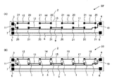
従って、基板上に複数のLEDを直線状に配置して直列接続したLEDモジュールは、図25、26に示すように直列接続した複数のLED1の両端のアノードとカソードを外部に引き出すためのアノード端子3とカソード端子4が基板2上に設けられている。この場合、図25のように、アノード端子3とカソード端子4を基板2の一方端に寄せて配置する第1のケースと、図26のように、アノード端子3を基板2の一方端に配置し、カソード端子4を基板2の対向する他方端に配置する第2のケースが考えられる。図25、26に示すケースでは、一例として、8個のLEDを直列に接続したLEDモジュール50、51を示す。但し、図25(A)、26(A)は、夫々LEDを実装する前の状態を示し、図25(B)、26(B)では、夫々LEDを実装した状態を示している。
Therefore, an LED module in which a plurality of LEDs are arranged in a straight line on a substrate and connected in series, as shown in FIGS. 25 and 26, an anode terminal for pulling out the anodes and cathodes at both ends of the plurality of
各LEDモジュール50、51には、絶縁基板2上に、8個のLED1を直列接続するための9本の連結用配線11〜19が形成されており、各連結用配線11〜19は、相互に離間し、端部同士が近接して連続的に配置されている。第1の連結用配線11の一方端はアノード端子3と接続し、他方端には1つのLEDのアノードと接続するための電極20が形成され、第2〜第8の連結用配線12〜18の各一方端には、夫々LEDのカソードと接続するための電極21が、各他方端には、夫々LEDのアノードと接続するための電極20が形成され、第9の連結用配線19の一方端はカソード端子4と接続し、他方端には1つのLEDのカソードと接続するための電極21が形成されている。隣接する連結用配線の近接する端部に設けられた電極20、21間に夫々LEDのアノードとカソードを接続することで、アノード端子3とカソード端子4間に8個のLED1が順方向に直列接続したLEDモジュールとなる。
In each of the
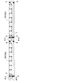
図25に示すアノード端子3とカソード端子4が基板の一方端に寄せて配置されたLEDモジュール50を2×4のマトリクス状に配置してLEDを平面的に配置したLED光源装置を構成する場合の外部配線の構成図を図27に示す。例えば、図27のように、各LEDモジュール50を並列に構成する場合は、各LEDモジュール50のLEDを駆動し、その発光を制御する制御基板42を外部に設け、各LEDモジュール50のアノード端子3及びカソード端子4と制御基板42を接続する外部配線52が、合計で16本必要となり、しかも、制御基板42と離れて配置されたLEDモジュール50からの外部配線の引き回しが長くなっている。ここで、外部配線は、LEDモジュールの外部における配線を意味し、LEDモジュール内の基板上に形成された連結用配線と区別するために、「外部配線」と称している。
A case where an LED light source device in which LEDs are arranged in a plane by arranging
また、図26に示すLEDモジュール51を2×4のマトリクス状に配置してLEDを平面的に配置したLED光源装置を構成する場合の配線の構成図を図28に示す。図25に示すLEDモジュール50と比べると、アノード端子3とカソード端子4が対辺に分かれて配置されているため、各LEDモジュール50のアノード端子3及びカソード端子4と制御基板42を接続する外部配線52の本数は、LEDモジュール50と同じく16本であるが、外部配線の引き回しが更に長くなっている。
FIG. 28 shows a wiring configuration diagram in the case where an LED light source device in which the
ここで、2個のLEDモジュール50または51に実装されたLEDを直列に接続すると、図29及び図30に示すように、各LEDモジュール50のアノード端子3及びカソード端子4と制御基板42を接続する外部配線52が半減するが、依然として長い引き回しの外部配線が存在している。
Here, when the LEDs mounted on the two
以上のように、LEDモジュールを複数用いて、LEDを面状に複数配列してバックライト等の光源装置を構成する場合に、アノード端子とカソード端子の配置個所に関係なく、LEDモジュールと制御基板間を接続する配線の引き回しが生じるが、光源装置の照射面積に対してLEDモジュールが小さく、使用するLEDモジュールの個数が多くなるほど当該配線の引き回しが長くなり、実装上問題となる。そこで、照射面積が大きいほどLED搭載数の多い大きなLEDモジュールを使用すれば良いが、そうすると、光源装置の照射面積に対応してLEDモジュールを多種用意しなければならないという欠点が生じる。 As described above, when a light source device such as a backlight is configured by using a plurality of LED modules and arranging a plurality of LEDs in a planar shape, the LED module and the control board regardless of the arrangement location of the anode terminal and the cathode terminal. However, the LED module is smaller than the irradiation area of the light source device, and the larger the number of LED modules to be used, the longer the wiring is routed, resulting in a mounting problem. Therefore, a larger LED module having a larger number of LEDs mounted may be used as the irradiation area is larger. However, in this case, there is a disadvantage that various LED modules must be prepared corresponding to the irradiation area of the light source device.
本発明は、LEDモジュールを複数用いて光源装置を構成する場合の配線の引き回しの問題に鑑みてなされたものであり、その目的は、簡単な配線によって光源装置を構成可能なLEDモジュールを提供することにある。 The present invention has been made in view of the problem of wiring routing when a light source device is configured using a plurality of LED modules, and an object of the present invention is to provide an LED module that can configure the light source device with simple wiring. There is.
上記目的を達成するため、本発明では、平板状の絶縁基板と、前記絶縁基板の第1の端辺の近傍に形成された外部回路との接続用の第1主端子と第1副端子と、前記絶縁基板の前記第1の端辺と対向する第2の端辺の近傍に形成された外部回路との接続用の第2主端子と第2副端子と、前記絶縁基板上に形成され、相互に離間して連続的に配置されたLEDを直列接続するための3以上の連結用配線と、隣接する前記連結用配線間に各別に接続され同方向に直列接続した複数のLEDと、前記絶縁基板上に形成され、前記第1副端子と前記第2副端子間を電気的に接続する第1通過配線と、前記絶縁基板上に形成され、短絡用の2端子素子の各端子と接続するための1対の接続用電極と、を備え、連続的に配置された前記3以上の連結用配線の内の一方端側に位置する1つの前記連結用配線である第1連結用配線が前記第1主端子と電気的に接続し、連続的に配置された前記3以上の連結用配線の内の他方端側に位置する他の1つの前記連結用配線である第2連結用配線が前記第2主端子と電気的に接続しているとともに、前記1対の接続用電極の一方が前記第1連結用配線または前記第2連結用配線と電気的に接続し、前記1対の接続用電極の他方が前記第1通過配線と電気的に接続していることを特徴とするLEDモジュールを提供する。 In order to achieve the above object, in the present invention, a first main terminal and a first sub-terminal for connecting a flat insulating substrate and an external circuit formed in the vicinity of the first end of the insulating substrate A second main terminal and a second sub-terminal for connecting to an external circuit formed in the vicinity of the second end opposite to the first end of the insulating substrate; and formed on the insulating substrate. Three or more connecting wirings for serially connecting LEDs that are continuously spaced apart from each other, and a plurality of LEDs that are separately connected between the adjacent connecting wirings and connected in series in the same direction, A first passage wiring formed on the insulating substrate and electrically connecting the first sub-terminal and the second sub-terminal ; and each terminal of a short-circuiting two-terminal element formed on the insulating substrate; and a connection electrode pair for connecting continuously arranged the three or more connecting wires A first connecting wire, which is one of the connecting wires located on one end side of the inside, is electrically connected to the first main terminal, and is one of the three or more connecting wires arranged continuously. A second connection wiring which is another one of the connection wirings located on the other end side is electrically connected to the second main terminal, and one of the pair of connection electrodes is the first connection wiring. Provided is an LED module that is electrically connected to a connection wiring or the second connection wiring, and the other of the pair of connection electrodes is electrically connected to the first passage wiring. .
上記特徴のLEDモジュールによれば、第1通過配線を外部配線の一部として使用できるため、LEDモジュールを複数配列する場合に生じる外部配線の引き回しを大幅に軽減することができる。特に、LEDモジュールを制御基板から離間する方向に一列に複数配列し、当該複数のLEDモジュールに搭載されたLEDを全て直列に接続する場合には、隣接する2つのLEDモジュール間で、第1の端辺の近傍に配置された第1主端子と第2の端辺の近傍に配置された第2主端子を電気的に接続し、第1の端辺の近傍に配置された第1副端子と第2の端辺の近傍に配置された第2副端子を電気的に接続し、制御基板から最も遠方に位置するLEDモジュールの遠方端の第1または第2の端辺の近傍に配置された第1または第2主端子と、第1または第2副端子を電気的に接続することで、全てのLEDを直列接続したLEDモジュール列が、外部配線の引き回しを伴わずに構成でき、当該LEDモジュール列を複数設けた光源装置では、外部配線の大幅な簡素化が図れる。また、1対の接続用電極を予め用意しておくことで、上述のように、LEDモジュールを制御基板から離間する方向に一列に複数配列し、当該複数のLEDモジュールに搭載されたLEDを全て直列に接続する場合において、制御基板から最も遠方に位置するLEDモジュールの遠方端の第1または第2の端辺の近傍に配置された第1または第2主端子と、第1または第2副端子を電気的に接続することが、当該1対の接続用電極間に短絡用の2端子素子を接続することで実現できる。つまり、短絡用の2端子素子の接続をLEDの実装作業と同時に行うことで、上述の主端子と副端子を導線等の外部配線で電気的に接続する手間が省略できる。 According to the LED module having the above characteristics, since the first passing wiring can be used as a part of the external wiring, it is possible to greatly reduce the routing of the external wiring that occurs when a plurality of LED modules are arranged. In particular, when a plurality of LED modules are arranged in a line in a direction away from the control board, and all the LEDs mounted on the plurality of LED modules are connected in series, the first LED is connected between two adjacent LED modules. A first sub-terminal disposed in the vicinity of the first end, electrically connecting the first main terminal disposed in the vicinity of the end side and the second main terminal disposed in the vicinity of the second end side And the second subterminal arranged in the vicinity of the second end side are electrically connected, and are arranged in the vicinity of the first or second end side of the farthest end of the LED module located farthest from the control board. By electrically connecting the first or second main terminal and the first or second sub-terminal, an LED module row in which all LEDs are connected in series can be configured without routing external wiring, In a light source device provided with a plurality of LED module rows Significant simplification of the external wiring can be achieved. In addition, by preparing a pair of connection electrodes in advance, as described above, a plurality of LED modules are arranged in a row in a direction away from the control board, and all the LEDs mounted on the plurality of LED modules are arranged. When connected in series, the first or second main terminal disposed in the vicinity of the first or second end side at the far end of the LED module located farthest from the control board, and the first or second sub-terminal The terminals can be electrically connected by connecting a short-circuiting two-terminal element between the pair of connection electrodes. That is, the connection of the two-terminal element for short-circuiting is performed simultaneously with the LED mounting operation, thereby eliminating the trouble of electrically connecting the main terminal and the sub-terminal with external wiring such as a conductor.
更に、上記特徴のLEDモジュールは、前記3以上の連結用配線が、前記絶縁基板の一方側の面上に形成され、前記第1通過配線が、前記絶縁基板の他方側の面上に形成されていることが好ましい。ここで、前記第1主端子と前記第2主端子と前記3以上の連結用配線を同一面上に形成し、前記第1副端子と前記第2副端子と前記第1通過配線を同一面上に形成しても良い。これにより、第1通過配線を絶縁基板の他方側の面上を専有して形成できるため、配線面積を大幅に拡大できる。この結果、絶縁基板の一方側の面上に搭載されるLEDの発熱で加熱された絶縁基板の熱を、第1通過配線によって絶縁基板の他方側への放熱でき、LEDモジュールの放熱性能が向上する。更に、第1通過配線の線幅も拡張されるため、第1通過配線の低インピーダンス化が図れる。 Further, in the LED module having the above characteristics, the three or more connection wirings are formed on one surface of the insulating substrate, and the first passing wiring is formed on the other surface of the insulating substrate. It is preferable. Here, the first main terminal, the second main terminal, and the three or more connecting wires are formed on the same surface, and the first sub terminal, the second sub terminal, and the first passing wire are formed on the same surface. It may be formed on top. Thereby, since the 1st passage wiring can be formed exclusively on the surface of the other side of an insulating substrate, wiring area can be expanded greatly. As a result, the heat of the insulating substrate heated by the heat generated by the LED mounted on one surface of the insulating substrate can be radiated to the other side of the insulating substrate by the first passing wiring, and the heat dissipation performance of the LED module is improved. To do. Furthermore, since the line width of the first passage wiring is expanded, the impedance of the first passage wiring can be reduced.
更に、上記特徴のLEDモジュールは、前記絶縁基板に内壁面が金属で被覆された貫通孔が複数形成されていることが好ましい。これにより、絶縁基板の一方側の面上に搭載されるLEDの発熱を他方側へ貫通孔を介して伝導して放熱することができ、LEDモジュールの放熱性能が向上する。更には、前記第1通過配線が前記絶縁基板の両方の面上に形成され、前記絶縁基板の一方側の面上に形成された前記第1通過配線と、前記絶縁基板の他方側の面上に形成された前記第1通過配線が、前記絶縁基板に複数形成された内壁面が金属で被覆された貫通孔を介して電気的に接続していることが好ましい。絶縁基板に両方の面上に第1通過配線を設けて貫通孔で連結することで、LEDモジュールの放熱性能が更に向上するとともに、第1通過配線の更なる低インピーダンス化が図れる。 Furthermore, in the LED module having the above characteristics, it is preferable that a plurality of through holes whose inner wall surfaces are coated with metal are formed on the insulating substrate. As a result, the heat generated by the LED mounted on one surface of the insulating substrate can be conducted to the other side through the through-hole to radiate heat, and the heat radiation performance of the LED module is improved. Further, the first passing wiring is formed on both surfaces of the insulating substrate, the first passing wiring formed on one surface of the insulating substrate, and the other surface of the insulating substrate. It is preferable that a plurality of the first passing wirings are electrically connected through a through hole in which a plurality of inner wall surfaces formed on the insulating substrate are covered with a metal. By providing the first passage wiring on both surfaces of the insulating substrate and connecting with the through holes, the heat dissipation performance of the LED module can be further improved and the impedance of the first passage wiring can be further reduced.
更に、上記特徴のLEDモジュールは、前記絶縁基板の他方側の面上に形成された前記第1通過配線が、前記絶縁基板の内部に向けて突出する突起部を備えていることが好ましい。絶縁基板の他方側の面上に形成された第1通過配線に突起部を備えることで、第1通過配線と絶縁基板との接触面積が拡大するため、絶縁基板の一方側の面上に搭載されるLEDの発熱で加熱された絶縁基板の熱を、第1通過配線によって絶縁基板の他方側へのより効率的に放熱することができる。 Furthermore, in the LED module having the above characteristics, it is preferable that the first passing wiring formed on the other surface of the insulating substrate includes a protrusion protruding toward the inside of the insulating substrate. Since the contact area between the first passing wiring and the insulating substrate is increased by providing the first passing wiring formed on the other surface of the insulating substrate, the mounting is performed on the one surface of the insulating substrate. The heat of the insulating substrate heated by the heat generated by the LED can be radiated more efficiently to the other side of the insulating substrate by the first passage wiring.
更に、本発明では、上記特徴のLEDモジュールを、1つの前記LEDモジュールの前記第1の端辺と、他の1つの前記LEDモジュールの前記第2の端辺を近接させて第1方向に複数配列し、近接する前記第1の端辺の近傍に配置された前記主端子の1つと前記第2の端辺の近傍に配置された前記主端子の1つを電気的に接続し、近接する前記第1の端辺の近傍に配置された前記副端子の1つと前記第2の端辺の近傍に配置された前記副端子の1つを電気的に接続してLEDモジュール列を構成し、前記LEDモジュール列を、前記第1方向と直交する第2方向に複数配列して、前記LEDモジュールに実装されている前記LEDを面状に複数配列することを特徴とするLED光源装置を提供する。 Furthermore, in the present invention, a plurality of the LED modules having the above characteristics are arranged in the first direction by bringing the first end of one LED module close to the second end of the other LED module. Arranging and electrically connecting one of the main terminals arranged in the vicinity of the adjacent first edge and one of the main terminals arranged in the vicinity of the second edge One of the sub terminals arranged in the vicinity of the first end side and one of the sub terminals arranged in the vicinity of the second end side are electrically connected to form an LED module row, Provided is an LED light source device in which a plurality of the LED module rows are arranged in a second direction orthogonal to the first direction, and a plurality of the LEDs mounted on the LED module are arranged in a planar shape. .
上記特徴のLED光源装置によれば、LEDモジュールと制御基板間、或いは、LEDモジュール間の外部配線の引き回しを大幅に軽減した簡単な配線構造のLED光源装置が提供可能となる。 According to the LED light source device having the above characteristics, it is possible to provide an LED light source device having a simple wiring structure that greatly reduces the routing of external wiring between the LED module and the control board or between the LED modules.
本発明に係るLEDモジュール、及び、LED光源装置の実施形態につき、図面に基づいて説明する。尚、以下において、説明の理解の容易のため、図25、26に示す従来のLEDモジュール、及び、各実施形態間で共通する部位には同じ符号を付して説明する。 Embodiments of an LED module and an LED light source device according to the present invention will be described with reference to the drawings. In the following, for easy understanding of the description, the conventional LED module shown in FIGS. 25 and 26 and parts common to the embodiments will be described with the same reference numerals.
〈第1実施形態〉
図1に、本発明によるLEDモジュールの第1実施形態の概略構成を模式的に示す。図1(A)は、LEDを実装する前のプリント配線基板30’を示し、図1(B)は、LED1を実装後のLEDモジュール30を示す。
<First Embodiment>
FIG. 1 schematically shows a schematic configuration of a first embodiment of an LED module according to the present invention. FIG. 1A shows a printed
プリント配線基板30’は、絶縁基板2上に、8個のLED1を直列接続するための9本の連結用配線11〜19と、外部回路と接続用の第1主端子3、第2主端子4、第1副端子5、及び、第2副端子6の4端子と、第1副端子5と第2副端子6間を電気的に接続する第1通過配線8が形成されて構成される。絶縁基板2は、ガラスエポキシ等の絶縁素材で構成され、連結用配線11〜19、4つの端子3〜6、第1通過配線8は、銅箔等の金属膜で構成される。
The printed
各連結用配線11〜19は、相互に離間し、端部同士が近接して連続的に配置されている。左端の連結用配線11(第1連結用配線に相当)の一方端は第1主端子3と接続し、他方端には1つのLEDのアノードと接続するための電極20が形成され、中央の6個の連結用配線12〜18の各一方端には、夫々LEDのカソードと接続するための電極21が、各他方端には、夫々LEDのアノードと接続するための電極20が形成され、右端の連結用配線19(第2連結用配線に相当)の一方端は第2主端子4と接続し、他方端には1つのLEDのカソードと接続するための電極21が形成されている。電極20、21は、連結用配線11〜19の端部として同じ材料で形成されている。隣接する連結用配線の近接する端部に設けられた電極20、21間に夫々LEDのアノードとカソードを接続することで、第1主端子3と第2主端子4間に8個のLED1が順方向に直列接続する。従って、本実施形態では、第1主端子3がアノード端子となり、第2主端子4がカソード端子となる。
The connection wirings 11 to 19 are spaced apart from each other and are continuously arranged with their end portions close to each other. One end of the leftmost connecting wire 11 (corresponding to the first connecting wire) is connected to the first
第1主端子3と第2主端子4が、絶縁基板2の対向する2辺に夫々分離して配置され、第1副端子5と第2副端子6が絶縁基板2の対向する2辺に夫々分離して配置され、一連の連結用配線11〜19と第1通過配線8が、夫々、絶縁基板2を長手方向に横断するように形成されている。
The first
本実施形態では、LED1として表面実装型のLEDを想定し、LED1のアノードとカソードは平面的な金属膜(ランド)で形成された電極20、21に半田リフロー等によって電気的に接続され、LED1が電極20、21間に表面実装される。尚、LED1がリード型の場合では、電極20、21は、半田付け用の金属膜(ランド)とその中央に形成されたリード端子を挿入するスルーホール(貫通孔)で構成される。
In the present embodiment, a surface-mount type LED is assumed as the
次に、図1に示すLEDモジュール30を2個接続して、合計16個のLEDを直列接続する場合の外部配線41a〜41eの接続方法について、図2を用いて説明する。
Next, a method of connecting the
外部配線41a、41bは、LEDモジュール30の各LEDを駆動し、その発光を制御する図示しない制御基板のアノード駆動端子とカソード駆動端子を、一方のLEDモジュール30aの第1主端子3と、他方のLEDモジュール30bの第2主端子4に夫々接続するための外部配線である。本実施形態では、外部配線41aはLEDモジュール30aの第1主端子3と直接接続し、外部配線41bはLEDモジュール30aの第1副端子5と直接接続している。
The
外部配線41c、41dは、2つのLEDモジュール30a、30b間を接続するための外部配線である。本実施形態では、外部配線41cはLEDモジュール30aの第2主端子4とLEDモジュール30bの第1主端子3間を直接接続し、外部配線41dはLEDモジュール30aの第2副端子6とLEDモジュール30bの第1副端子5間を直接接続している。外部配線41eは、制御基板から遠方側のLEDモジュール30bの端辺に配置されている第2主端子4と第2副端子6の終端処理するための外部配線で、当該両端子間を接続して短絡する。
The
外部配線41cによって、LEDモジュール30aの第1主端子3とLEDモジュール30bの第2主端子4間において、16個のLED1が直列接続し、外部配線41d、41eによって、LEDモジュール30bの第2主端子4とLEDモジュール30aの第1副端子5間が、2つのLEDモジュール30a、30bの各第1通過配線8を介して電気的に接続され、外部配線41bとLEDモジュール30bの第2主端子4が電気的に接続される。この結果、直列接続した16個のLEDが、5本の短い外部配線41a〜41eによって制御基板から駆動及び制御可能となる。
Sixteen
外部配線41a〜41eとLEDモジュール30の各端子3〜6間の接続方法としては、外部配線41a〜41eが導線の場合は、導線の先端を各端子の表面に半田付けする方法、外部配線41a〜41eを2ピンコネクタで構成した場合、第1主端子3と第1副端子5に接続する第1の2ピンコネクタを絶縁基板2の対向する2辺の一方に設け、第2主端子4と第2副端子6に接続する第2の2ピンコネクタを絶縁基板2の対向する2辺の他方に設け、隣接する2つのLEDモジュール30間で、第1の2ピンコネクタと第2の2ピンコネクタを接続する方法等が想定される。
As a connection method between the
図2に示す構成と、図29または図30に示す従来の構成と比較すると、外部配線の引き回しが大幅に低減されていることが分かる。 Comparing the configuration shown in FIG. 2 with the conventional configuration shown in FIG. 29 or FIG. 30, it can be seen that the routing of the external wiring is greatly reduced.
更に、図1に示すLEDモジュール30を3個以上接続して、LEDの直列段数を8n(nは3以上の整数)とする場合には、図3に示すように、3個目からのLEDモジュール30cを2つのLEDモジュール30a、30bの間に挿入し、図2に示す構成と同様に、LEDモジュール30aの第2主端子4とLEDモジュール30cの第1主端子3間と、LEDモジュール30cの第2主端子4とLEDモジュール30bの第1主端子3間を、夫々外部配線41cで直接接続し、LEDモジュール30aの第2副端子6とLEDモジュール30cの第1副端子5間と、LEDモジュール30cの第2副端子6とLEDモジュール30bの第1副端子5間とを、夫々外部配線41dで直接接続する。更に、追加するLEDモジュール30cが2以上の場合は、LEDモジュール30cの第2主端子4と隣接するLEDモジュール30cの第1主端子3間を外部配線41cで直接接続し、LEDモジュール30cの第2副端子6と隣接するLEDモジュール30cの第1副端子5間を外部配線41dで直接接続する。図3に示すように、LEDモジュール30を、一方の第2主端子4と第2副端子6が配置された端辺と、他方の第1主端子3と第1副端子5が配置された端辺同士を近接させて、順番に配置し、外部配線41c、41dで接続することで、簡単にLEDの直列段数を増加することができる。尚、図3では、各LEDモジュール30のLED1、連結用配線11〜19、電極20、21、第1通過配線8の図示を省略している。
Further, when three or
本実施形態では、図2及び図3に示すように、外部配線41aをLEDモジュール30aの第1主端子3と直接接続し、外部配線41bをLEDモジュール30aの第1副端子5と直接接続する構成としたが、図4及び図5に示すように、LEDモジュール30の夫々を180度回転させて、外部配線41aをLEDモジュール30aの第2副端子6と直接接続し、外部配線41bをLEDモジュール30aの第2主端子4と直接接続する構成としても良い。この場合、外部配線41c、41dは、図2及び図3に示す構成と同様に、隣接するLEDモジュール30間の第1主端子3と第2主端子4間、及び、第1副端子5と第2副端子6間を夫々接続しており、また、外部配線41eは、図2及び図3に示す構成とは異なり、制御基板から遠方側のLEDモジュール30bの端辺に配置されている第1主端子3と第1副端子5間を接続して短絡している。
In the present embodiment, as shown in FIGS. 2 and 3, the
〈第2実施形態〉
次に、本発明によるLEDモジュールの第2実施形態について説明する。図6に、本発明によるLEDモジュールの第2実施形態の概略構成を模式的に示す。図6(A)は、LEDを実装する前のプリント配線基板31’を示し、図6(B)は、LED1を実装後のLEDモジュール31(31a)を示し、図6(C)は、LED1と短絡用素子22を実装後のLEDモジュール31(31b)を示す。
Second Embodiment
Next, a second embodiment of the LED module according to the present invention will be described. FIG. 6 schematically shows a schematic configuration of a second embodiment of the LED module according to the present invention. 6A shows the printed
プリント配線基板31’は、絶縁基板2上に、8個のLED1を直列接続するための9本の連結用配線11〜19と電極20、21、外部回路と接続用の第1主端子3、第2主端子4、第1副端子5、及び、第2副端子6の4端子と、第1副端子5と第2副端子6間を電気的に接続する第1通過配線8、連結用配線19(第2連結用配線に相当)と電気的に接続する電極23、第1通過配線8と電気的に接続する電極24が形成されて構成される。絶縁基板2は、ガラスエポキシ等の絶縁素材で構成され、連結用配線11〜19、4つの端子3〜6、第1通過配線8、電極20、21、23、24は、銅箔等の金属膜で構成される。
The printed
第2実施形態のプリント配線基板31’は、第1実施形態のプリント配線基板30’に対して、電極23、24が新たに追加されている点で相違するものであり、電極23、24以外の構成要素については、第1実施形態と同じであるので、重複する説明は割愛する。
The printed
電極23、24は、短絡用素子22を実装するための電極で、電極20、21と同様に互いに1対として相互に近接して配置されている。短絡用素子22は、LED1と同様に表面実装型の2端子型素子で、チップ型抵抗素子の抵抗体を導電体で置き換えて抵抗値を実質的に0Ωとしたものであり、ジャンパー線等で置き換えても良い。短絡用素子22は、LED1の電極20、21への実装時に並行して、電極23、24に半田リフロー等によって電気的に接続されて、LEDモジュール31bが形成される。第2実施形態では、同じプリント配線基板31’を用いて、短絡用素子22を実装したLEDモジュール31bと、実装していないLEDモジュール31aの2種類のLEDモジュール31が作製される。
The
次に、図6に示すLEDモジュール31a、31bを1個ずつ接続して、合計16個のLEDを直列接続する場合の外部配線41a〜41dの接続方法について、図7を用いて説明する。
Next, a method of connecting the
外部配線41a〜41dについては、第1実施形態と同様に、外部配線41aはLEDモジュール31aの第1主端子3と直接接続し、外部配線41bはLEDモジュール31aの第1副端子5と直接接続し、外部配線41cはLEDモジュール31aの第2主端子4とLEDモジュール31bの第1主端子3間を直接接続し、外部配線41dはLEDモジュール31aの第2副端子6とLEDモジュール31bの第1副端子5間を直接接続している。第1実施形態と相違する点は、第1実施形態では、制御基板から遠方側のLEDモジュール30bの端辺に配置されている第2主端子4と第2副端子6間を、外部配線41eによって接続して短絡していたのに対し、第2実施形態では、制御基板から遠方側のLEDモジュール31bの端辺に配置されている第2主端子4と第2副端子6間を、外部配線ではなく、電極23、24間を短絡用素子22で接続して短絡することで、連結用配線19を介して電極23と電気的に接続する第2主端子4と、第1通過配線8を介して電極24と電気的に接続する第2副端子6間が短絡される。この結果、当該短絡処理を、プリント配線基板31’へのLED1の実装時に同時に行えるため、外部配線41eの接続処理が省略でき、外部配線41a〜41dの接続処理が簡素化できる。
As for the
外部配線41cによって、LEDモジュール31aの第1主端子3とLEDモジュール31bの第2主端子4間において、16個のLED1が直列接続し、外部配線41dと短絡用素子22によって、LEDモジュール31bの第2主端子4とLEDモジュール31aの第1副端子5間が、2つのLEDモジュール31a、31bの各第1通過配線8を介して電気的に接続され、外部配線41bとLEDモジュール31bの第2主端子4が電気的に接続される。この結果、直列接続した16個のLEDが、4本の短い外部配線41a〜41dと短絡用素子22によって制御基板から駆動及び制御可能となる。
Sixteen
第2実施形態と第1実施形態の相違点は、制御基板から遠方側のLEDモジュール31b(30b)の端辺に配置されている第2主端子4と第2副端子6間の短絡処理の仕方が異なるだけであるので、第1実施形態と同様に、図29または図30に示す従来の構成と比較すると、外部配線の引き回しが大幅に低減されていることが分かる。更に、図6に示すLEDモジュール31を3個以上接続して、LEDの直列段数を8n(nは3以上の整数)とする場合についても、図8に示すように、3個目からのLEDモジュール31cを2つのLEDモジュール31a、31bの間に挿入し、図7に示す構成と同様に、LEDモジュール31aの第2主端子4とLEDモジュール31cの第1主端子3間と、LEDモジュール31cの第2主端子4とLEDモジュール31bの第1主端子3間を、夫々外部配線41cで直接接続し、LEDモジュール31aの第2副端子6とLEDモジュール31cの第1副端子5間と、LEDモジュール31cの第2副端子6とLEDモジュール31bの第1副端子5間とを、夫々外部配線41dで直接接続する。更に、追加するLEDモジュール31cが2以上の場合は、LEDモジュール31cの第2主端子4と隣接するLEDモジュール31cの第1主端子3間を外部配線41cで直接接続し、LEDモジュール31cの第2副端子6と隣接するLEDモジュール31cの第1副端子5間を外部配線41dで直接接続する。図8に示すように、LEDモジュール31を、第2主端子4と第2副端子6が配置された一方の端辺と、第1主端子3と第1副端子5が配置された他方の端辺同士を近接させて、順番に配置し、外部配線41c、41dで接続することで、簡単にLEDの直列段数を増加することができる。但し、2つのLEDモジュール31a、31bの間に挿入する3個目からのLEDモジュール31cは、LEDモジュール31aと同様に短絡用素子22の実装されていないLEDモジュール31である。尚、図8では、各LEDモジュール31のLED1、連結用配線11〜19、電極20、21、第1通過配線8、短絡用素子22、電極23、24の図示を省略している。
The difference between the second embodiment and the first embodiment is that the short-circuiting process between the second
〈第3実施形態〉
次に、本発明によるLEDモジュールの第3実施形態について説明する。図9に、本発明によるLEDモジュールの第3実施形態の概略構成を模式的に示す。第2実施形態では、図6に示すように、電極23を連結用配線19(第2連結用配線に相当)と電気的に接続するように設け、第1通過配線8と電気的に接続する電極24と近接するように形成したが、第3実施形態では、図9に示すように、電極23を連結用配線11(第1連結用配線に相当)と電気的に接続するように設ける。図9(A)は、LEDを実装する前のプリント配線基板32’を示し、図9(B)は、LED1を実装後のLEDモジュール32(32a)を示し、図9(C)は、LED1と短絡用素子22を実装後のLEDモジュール32(32b)を示す。
<Third Embodiment>
Next, a third embodiment of the LED module according to the present invention will be described. FIG. 9 schematically shows a schematic configuration of a third embodiment of the LED module according to the present invention. In the second embodiment, as shown in FIG. 6, the
第3実施形態のプリント配線基板32’は、第2実施形態のプリント配線基板31’に対して、電極23の電気的な接続先が相違するだけであり、LEDモジュール32の各構成要素については、第1及び第2実施形態と同じであるので、重複する説明は割愛する。
The printed
次に、図9に示すLEDモジュール32a、32bを1個ずつ接続して、合計16個のLEDを直列接続する場合の外部配線41a〜41dの接続方法について、図10を用いて説明する。外部配線41a〜41dの接続方法が、第2実施形態とは異なり、第1実施形態の図4に示す接続方法と類似する。外部配線41aはLEDモジュール32aの第2副端子6と直接接続し、外部配線41bはLEDモジュール32aの第2主端子4と直接接続する。外部配線41cはLEDモジュール32aの第1主端子3とLEDモジュール32bの第2主端子4間を直接接続し、外部配線41dはLEDモジュール32aの第1副端子5とLEDモジュール32bの第2副端子6間を直接接続している。
Next, a method of connecting the
第1実施形態の図4の接続方法と相違する点は、第1実施形態の図4では、制御基板から遠方側のLEDモジュール30bの端辺に配置されている第1主端子3と第1副端子5間を、外部配線41eによって接続して短絡していたのに対し、第3実施形態では、制御基板から遠方側のLEDモジュール32bの端辺に配置されている第1主端子3と第1副端子5間を、外部配線ではなく、電極23、24間を短絡用素子22で接続して短絡することで、連結用配線11を介して電極23と電気的に接続する第1主端子3と、第1通過配線8を介して電極24と電気的に接続する第1副端子5間が短絡される。この結果、当該短絡処理を、プリント配線基板32’へのLED1の実装時に同時に行えるため、外部配線41eの接続処理が省略でき、外部配線41a〜41dの接続処理が簡素化できる。
The difference from the connection method of FIG. 4 of the first embodiment is that in FIG. 4 of the first embodiment, the first
外部配線41cによって、LEDモジュール32aの第2主端子4とLEDモジュール32bの第1主端子3間において、第2実施形態とは逆方向に16個のLED1が直列接続し、外部配線41dと短絡用素子22によって、LEDモジュール32bの第1主端子3とLEDモジュール32aの第2副端子6間が、2つのLEDモジュール32a、32bの各第1通過配線8を介して電気的に接続され、外部配線41aとLEDモジュール32bの第1主端子3が電気的に接続される。この結果、直列接続した16個のLEDが、4本の短い外部配線41a〜41dと短絡用素子22によって制御基板から駆動及び制御可能となる。
By the
第3実施形態と第1実施形態の図4に示す構成の相違点は、制御基板から遠方側のLEDモジュール32b(30b)の端辺に配置されている第1主端子3と第1副端子5間の短絡処理の仕方が異なるだけであるので、第1実施形態と同様に、図29または図30に示す従来の構成と比較すると、外部配線の引き回しが大幅に低減されていることが分かる。更に、図9に示すLEDモジュール32を3個以上接続して、LEDの直列段数を8n(nは3以上の整数)とする場合についても、図11に示すように、3個目からのLEDモジュール32cを2つのLEDモジュール32a、32bの間に挿入し、図10に示す構成と同様に、LEDモジュール32aの第1主端子3とLEDモジュール32cの第2主端子4間と、LEDモジュール31cの第1主端子3とLEDモジュール32bの第2主端子4間を、夫々外部配線41cで直接接続し、LEDモジュール32aの第1副端子5とLEDモジュール32cの第2副端子6間と、LEDモジュール32cの第1副端子5とLEDモジュール32bの第2副端子6間とを、夫々外部配線41dで直接接続する。更に、追加するLEDモジュール32cが2以上の場合は、LEDモジュール32cの第1主端子3と隣接するLEDモジュール32cの第2主端子4間を外部配線41cで直接接続し、LEDモジュール32cの第1副端子5と隣接するLEDモジュール32cの第2副端子6間を外部配線41dで直接接続する。図11に示すように、LEDモジュール32を、第1主端子3と第1副端子5が配置された一方の端辺と、第2主端子4と第2副端子6が配置された他方の端辺同士を近接させて、順番に配置し、外部配線41c、41dで接続することで、簡単にLEDの直列段数を増加することができる。但し、2つのLEDモジュール32a、32bの間に挿入する3個目からのLEDモジュール32cは、LEDモジュール32aと同様に短絡用素子22の実装されていないLEDモジュール32である。尚、図11では、各LEDモジュール30のLED1、連結用配線11〜19、電極20、21、第1通過配線8、短絡用素子22、電極20、21の図示を省略している。
The difference between the third embodiment and the first embodiment shown in FIG. 4 is that the first
〈第4実施形態〉
次に、本発明によるLEDモジュールの第4実施形態について説明する。図12に、本発明によるLEDモジュールの第4実施形態の概略構成を模式的に示す。図12(A)は、LEDを実装する前のプリント配線基板33’を示し、図12(B)は、LED1を実装後のLEDモジュール33を示す。
<Fourth embodiment>
Next, a fourth embodiment of the LED module according to the present invention will be described. FIG. 12 schematically shows a schematic configuration of the fourth embodiment of the LED module according to the present invention. FIG. 12A shows a printed
プリント配線基板33’は、絶縁基板2上に、8個のLED1を直列接続するための9本の連結用配線11〜19と電極20、21、外部回路と接続用の第1主端子3、第2主端子4、第1副端子5、第2副端子6、及び、第3副端子7の5端子と、第1副端子5と第2副端子6間を電気的に接続する第1通過配線8、第3副端子7と連結用配線19(第2連結用配線に相当)間を電気的に接続する第2通過配線9が形成されて構成される。第4実施形態では、第3副端子7は、第1主端子3及び第1副端子5と同じ側の端辺近傍に配置されている。つまり、第2通過配線9は、第1通過配線8と同様に、絶縁基板2を長手方向に横断するように形成されている。絶縁基板2は、ガラスエポキシ等の絶縁素材で構成され、連結用配線11〜19、5つの端子3〜7、第1通過配線8、第2通過配線9、電極20、21は、銅箔等の金属膜で構成される。
The printed
第4実施形態のプリント配線基板33’は、第1実施形態のプリント配線基板30’に対して、第3副端子7と第2通過配線9が新たに追加されている点で相違するものであり、第3副端子7と第2通過配線9以外の構成要素については、第1実施形態と同じであるので、重複する説明は割愛する。第2通過配線9は、短絡用素子22を実装した第2実施形態のLEDモジュール31bにおける短絡用素子22に該当するもので、第1副端子5と第3副端子7を入れ替えて使用することで、短絡用素子22によって連結用配線19と第1通過配線8間を短絡させた場合と同じ効果、或いは、第1実施形態において制御基板から遠方側のLEDモジュール30bの端辺に配置されている第2主端子4と第2副端子6間を外部配線41eによって短絡させた場合と同じ効果が得られる。
The printed
次に、図12に示す2つのLEDモジュール33を接続して、合計16個のLEDを直列接続する場合の外部配線41a〜41dの接続方法について、図13を用いて説明する。
Next, a method of connecting the
第1及び第2実施形態と同様に、外部配線41aはLEDモジュール33aの第1主端子3と直接接続し、外部配線41bはLEDモジュール33aの第1副端子5と直接接続し、外部配線41cはLEDモジュール34aの第2主端子4とLEDモジュール33bの第1主端子3間を直接接続する。第1及び第2実施形態と異なり、外部配線41dはLEDモジュール33aの第2副端子6とLEDモジュール33bの第3副端子7間を直接接続している。第1及び第2実施形態と相違する点は、第1及び第2実施形態では、外部配線41dはLEDモジュール30a、31aの第2副端子6とLEDモジュール30b、31bの第1副端子5間を直接接続し、制御基板から遠方側のLEDモジュール30b、31bの端辺に配置されている第2主端子4と第2副端子6間を、外部配線41e或いは短絡用素子22によって短絡していたのに対し、第4実施形態では、外部配線41dはLEDモジュール33aの第2副端子6とLEDモジュール33bの第3副端子7間を直接接続し、制御基板から遠方側のLEDモジュール33bの端辺に配置されている第2主端子4と第2副端子6間の短絡処理は行わない。この結果、第1及び第2実施形態における外部配線41eまたは短絡用素子22による当該短絡処理を省略でき、外部配線41a〜41dの接続処理が簡素化できる。
As in the first and second embodiments, the
外部配線41cによって、LEDモジュール33aの第1主端子3とLEDモジュール33bの第2主端子4間において、16個のLED1が直列接続し、外部配線41dによって、LEDモジュール33bの第2主端子4とLEDモジュール33aの第1副端子5間が、LEDモジュール33aの第1通過配線8とLEDモジュール33bの第2通過配線9を介して電気的に接続され、外部配線41bとLEDモジュール33bの第2主端子4が電気的に接続される。この結果、直列接続した16個のLEDが、4本の短い外部配線41a〜41dによって制御基板から駆動及び制御可能となる。
Sixteen
第4実施形態と第1実施形態の相違点は、制御基板から遠方側のLEDモジュール33b(30b)の端辺に配置されている第2主端子4と、外部配線41bと接続するLEDモジュール33a(30a)の第1副端子5間を電気的に接続する仕方が異なるだけであるので、第1実施形態と同様に、図29または図30に示す従来の構成と比較すると、外部配線の引き回しが大幅に低減されていることが分かる。更に、図12に示すLEDモジュール33を3個以上接続して、LEDの直列段数を8n(nは3以上の整数)とする場合についても、図14に示すように、3個目からのLEDモジュール33cを2つのLEDモジュール33a、33bの間に挿入し、図13に示す構成と同様に、LEDモジュール33aの第2主端子4とLEDモジュール33cの第1主端子3間と、LEDモジュール33cの第2主端子4とLEDモジュール33bの第1主端子3間を、夫々外部配線41cで直接接続し、LEDモジュール33aの第2副端子6とLEDモジュール33cの第1副端子5間と、LEDモジュール33cの第2副端子6とLEDモジュール33bの第3副端子7間とを、夫々外部配線41dで直接接続する。更に、追加するLEDモジュール33cが2以上の場合は、LEDモジュール33cの第2主端子4と隣接するLEDモジュール33cの第1主端子3間を外部配線41cで直接接続し、LEDモジュール33cの第2副端子6と隣接するLEDモジュール33cの第1副端子5間を外部配線41dで直接接続する。図14に示すように、LEDモジュール33を、第2主端子4と第2副端子6が配置された一方の端辺と、第1主端子3と第1副端子5と第3副端子7が配置された他方の端辺同士を近接させて、順番に配置し、外部配線41c、41dで接続することで、簡単にLEDの直列段数を増加することができる。尚、図14では、各LEDモジュール33のLED1、連結用配線11〜19、電極20、21、第1通過配線8、第2通過配線9の図示を省略している。
The difference between the fourth embodiment and the first embodiment is that the
〈第5実施形態〉
次に、本発明によるLEDモジュールの第5実施形態について説明する。図15に、本発明によるLEDモジュールの第5実施形態の概略構成を模式的に示す。第4実施形態では、図12に示すように、第3副端子7を、第1主端子3及び第1副端子5と同じ側の端辺近傍に配置し、第2通過配線9を、第3副端子7と連結用配線19間を電気的に接続するように形成したが、第5実施形態では、図15に示すように、第3副端子7を、第2主端子4及び第2副端子6と同じ側の端辺近傍に配置し、第2通過配線9を第3副端子7と連結用配線11(第1連結用配線に相当)間を電気的に接続するように形成する。図15(A)は、LEDを実装する前のプリント配線基板34’を示し、図15(B)は、LED1を実装後のLEDモジュール34を示す。
<Fifth Embodiment>
Next, a fifth embodiment of the LED module according to the present invention will be described. FIG. 15 schematically shows a schematic configuration of the fifth embodiment of the LED module according to the present invention. In the fourth embodiment, as shown in FIG. 12, the third subterminal 7 is arranged in the vicinity of the end on the same side as the first
第5実施形態のプリント配線基板34’は、第4実施形態のプリント配線基板33’に対して、第3副端子7の配置個所と電気的な接続先が相違するだけであり、LEDモジュール34の各構成要素については、第1及び第4実施形態と同じであるので、重複する説明は割愛する。
The printed
次に、図15に示す2つのLEDモジュール34を接続して、合計16個のLEDを直列接続する場合の外部配線41a〜41dの接続方法について、図16を用いて説明する。外部配線41a〜41dの接続方法が、第4実施形態とは異なり、第1実施形態の図4に示す接続方法と類似する。外部配線41aはLEDモジュール34aの第2副端子6と直接接続し、外部配線41bはLEDモジュール34aの第2主端子4と直接接続する。外部配線41cはLEDモジュール34aの第1主端子3とLEDモジュール34bの第2主端子4間を直接接続し、外部配線41dはLEDモジュール34aの第1副端子5とLEDモジュール34bの第3副端子7間を直接接続している。
Next, a method of connecting the
第1実施形態の図4の接続方法及び第3実施形態と相違する点は、第1実施形態の図4及び第3実施形態では、制御基板から遠方側のLEDモジュール30bの端辺に配置されている第1主端子3と第1副端子5間を、外部配線41e或いは短絡用素子22によって短絡していたのに対し、第5実施形態では、外部配線41dはLEDモジュール34aの第1副端子5とLEDモジュール34bの第3副端子7間を直接接続し、制御基板から遠方側のLEDモジュール34bの端辺に配置されている第1主端子3と第1副端子5間の短絡処理は行わない。この結果、第1実施形態の図4及び第3実施形態における外部配線41eまたは短絡用素子22による当該短絡処理を省略でき、外部配線41a〜41dの接続処理が簡素化できる。
The connection method of FIG. 4 of the first embodiment and the third embodiment are different from the connection method of the first embodiment in FIGS. 4 and 3 at the end of the
外部配線41cによって、LEDモジュール34aの第1主端子3とLEDモジュール34bの第2主端子4間において、第4実施形態とは逆方向に16個のLED1が直列接続し、外部配線41dによって、LEDモジュール34bの第1主端子3とLEDモジュール34aの第2副端子6間が、LEDモジュール34aの第1通過配線8とLEDモジュール34bの第2通過配線9を介して電気的に接続され、外部配線41aとLEDモジュール34bの第1主端子3が電気的に接続される。この結果、直列接続した16個のLEDが、4本の短い外部配線41a〜41dによって制御基板から駆動及び制御可能となる。
Between the first
第5実施形態と第1実施形態の図4に示す構成の相違点は、制御基板から遠方側のLEDモジュール34b(30b)の端辺に配置されている第1主端子3と、外部配線41aと接続するLEDモジュール33a(30a)の第2副端子6間を電気的に接続する仕方が異なるだけであるので、第1実施形態の図4に示す構成と同様に、図29または図30に示す従来の構成と比較すると、外部配線の引き回しが大幅に低減されていることが分かる。更に、図15に示すLEDモジュール34を3個以上接続して、LEDの直列段数を8n(nは3以上の整数)とする場合についても、図17に示すように、3個目からのLEDモジュール34cを2つのLEDモジュール34a、34bの間に挿入し、図16に示す構成と同様に、LEDモジュール34aの第1主端子3とLEDモジュール34cの第2主端子4間と、LEDモジュール34cの第1主端子3とLEDモジュール34bの第2主端子4間を、夫々外部配線41cで直接接続し、LEDモジュール34aの第1副端子5とLEDモジュール34cの第2副端子6間と、LEDモジュール34cの第1副端子5とLEDモジュール34bの第3副端子7間とを、夫々外部配線41dで直接接続する。更に、追加するLEDモジュール34cが2以上の場合は、LEDモジュール34cの第1主端子3と隣接するLEDモジュール34cの第2主端子4間を外部配線41cで直接接続し、LEDモジュール34cの第1副端子5と隣接するLEDモジュール34cの第2副端子6間を外部配線41dで直接接続する。図17に示すように、LEDモジュール34を、第1主端子3と第1副端子5が配置された一方の端辺と、第2主端子4と第2副端子6と第3副端子7が配置された他方の端辺同士を近接させて、順番に配置し、外部配線41c、41dで接続することで、簡単にLEDの直列段数を増加することができる。尚、図17では、各LEDモジュール34のLED1、連結用配線11〜19、電極20、21、第1通過配線8、第2通過配線9の図示を省略している。
The difference between the fifth embodiment and the first embodiment shown in FIG. 4 is that the first
次に、第5実施形態のLEDモジュール34を複数用いて、各LEDモジュール34で直列接続した8個のLED1を夫々並列に接続する場合の外部配線41a〜41eの接続方法について、図18を参照して説明する。尚、図18に示す例では、LEDモジュール34を4個並列に接続する。図17に示す構成とは、各LEDモジュール34が180度回転して配置されている点で異なり、更に、外部配線41eを第1実施形態のように使用する点で異なる。外部配線41aはLEDモジュール34aの第1主端子3と直接接続し、外部配線41bはLEDモジュール34aの第1副端子5と直接接続する。外部配線41cはLEDモジュール34aの第3副端子7とLEDモジュール34cの第1主端子3間、LEDモジュール34cの第3副端子7とLEDモジュール34cの第1主端子3間、LEDモジュール34cの第3副端子7とLEDモジュール34bの第1主端子3間を夫々直接接続し、外部配線41dはLEDモジュール34aの第2副端子6とLEDモジュール34cの第1副端子5間、LEDモジュール34cの第2副端子6とLEDモジュール34cの第1副端子5間、LEDモジュール34cの第2副端子6とLEDモジュール34bの第1副端子5間を夫々直接接続している。外部配線41eは、4つのLEDモジュール34a、34b、34cの夫々の第2主端子4と第2副端子6間を直接接続している。
Next, referring to FIG. 18, a method for connecting the
図18に示す構成と、図27または図28に示す従来の構成とを比較すると、外部配線の引き回しが大幅に低減されていることが分かる。尚、第4実施形態のLEDモジュール33を複数用いても、同様の並列接続は可能である。
Comparing the configuration shown in FIG. 18 with the conventional configuration shown in FIG. 27 or FIG. 28, it can be seen that the routing of the external wiring is greatly reduced. Even when a plurality of
〈第6実施形態〉
次に、本発明によるLEDモジュールの第6実施形態について説明する。上記各実施形態では、9本の連結用配線11〜19と第1通過配線8を、絶縁基板2の同一面上に形成する場合について説明したが、連結用配線11〜19を絶縁基板2の一方の面上(例えば表面上)に形成し、第1通過配線8を他方の面上(例えば裏面上)に形成するのも好ましい。
<Sixth Embodiment>
Next, a sixth embodiment of the LED module according to the present invention will be described. In each of the above embodiments, the case where the nine connecting
図19に、第2実施形態のLEDモジュール31の別実施形態として、本発明によるLEDモジュールの第6実施形態の概略構成を模式的に示す。図19(A)は、LEDを実装する前のプリント配線基板35’の連結用配線11〜19が形成される側の第1面を示し、図19(B)は、LEDモジュール35の第1通過配線8が形成される側の第2面を示し、図19(C)は、LED1を実装後のLEDモジュール35(35a)の第1面を示し、図19(D)は、LED1と短絡用素子22を実装後のLEDモジュール35(35b)の第1面を示す。
FIG. 19 schematically shows a schematic configuration of a sixth embodiment of the LED module according to the present invention as another embodiment of the
プリント配線基板35’は、絶縁基板2の第1面上に、8個のLED1を直列接続するための9本の連結用配線11〜19と電極20、21、外部回路と接続用の第1主端子3と第2主端子4、及び、電極23と電極24が形成され、絶縁基板2の第2面上に、外部回路と接続用の第1副端子5と第2副端子6、及び、第1副端子5と第2副端子6間を電気的に接続する第1通過配線8が形成され、更に、絶縁基板2の第1面と第2面間を貫通し、内壁面に金属メッキ等により金属が被覆した貫通孔(スルーホール)であって、電極24と第1通過配線8と電気的に接続する第1貫通孔25が形成されて構成される。絶縁基板2は、ガラスエポキシ等の絶縁素材で構成され、連結用配線11〜19、4つの端子3〜6、第1通過配線8、電極20、21、23、24は、銅箔等の金属膜で構成される。
The printed
第6実施形態のプリント配線基板35’は、第2実施形態のプリント配線基板31’に対して、第1副端子5と第2副端子6と第1通過配線8を、第1主端子3と第2主端子4と連結用配線11〜19が形成される第1面とは反対の第2面に形成する点と、第1貫通孔25が新たに追加されている点で相違するものであり、第1貫通孔25以外の構成要素については、第1実施形態と同じであるので、重複する説明は割愛する。
The printed
第6実施形態では、第1通過配線8と連結用配線11〜19が、絶縁基板2の第1面と第2面に分離して形成されているため、第1通過配線8の専有面積及び線幅を第2実施形態に場合より大きくでき、LEDモジュール35の放熱性が向上するとともに、第1通過配線8の低インピーダンス化が図れる。放熱性については、絶縁基板2の第1面側にLED1が実装されるため、第1面側から加熱された絶縁基板2の熱を第2面側から、絶縁基板2より熱伝導性の高い第1通過配線8を介して放熱することができる。
In the sixth embodiment, since the
第6実施形態のLEDモジュール35は、第2実施形態のLEDモジュール31と電気的に等価なため、LEDモジュール35を連結して、LEDモジュール35に搭載されているLED1の直列段数をモジュール数倍に増加させる場合の外部配線41a〜41dの接続方法については、第2実施形態と基本的には同じであるが、外部配線41a、41cの接続は、絶縁基板2の第1面側で行い、外部配線41b、41dの接続は、絶縁基板2の第2面側で行う必要がある。図20に、LEDモジュール35a、35bを1個ずつ接続して、合計16個のLEDを直列接続する場合の外部配線41a〜41dの接続方法について示す。但し、外部配線41a〜41dの電気的な接続方法は、上述の通り、第2実施形態と同じであるので、重複する説明は割愛する。
Since the
図19に示すLEDモジュール35に対して、更に放熱性を向上させるために、図21に示すように、第1通過配線8を、絶縁基板2の第1面と第2面の両方に形成し、各面の第1通過配線8を多数の第2貫通孔26で電気的に接続したLEDモジュール36とするのも好ましい。第2貫通孔26は、第1貫通孔25と同様に形成される。図21(A)は、LEDを実装する前のLEDモジュール36(プリント配線基板36’)の第1面を示し、図21(B)は、LEDモジュール36の第2面を示す。図21に示すLEDモジュール36は多数の第2貫通孔26を備えることで、絶縁基板2の第1面側に実装されたLED1による発熱を、第1面側から第2貫通孔26を介して第2面側の第1通過配線8に伝導して、第1通過配線8から効率的に放熱することが可能となり、放熱性が、図19に示すLEDモジュール35より更に向上する。
In order to further improve the heat dissipation with respect to the
更に、図19及び図21に示すLEDモジュール35、36に対して、更に放熱性を向上させるために、図22の断面図に模式的に示すように、絶縁基板2の第2面側に形成される第1通過配線8に対して、絶縁基板2の内部に向けて(つまり、第1面側に向けて)突出する突起部27を、第1通過配線8の全面に分散して形成するのも好ましい。突起部27の断面形状は櫛形であり、平面形状は、例えば、ストライプ状、格子状、線状または十字状のものをマトリクス状に配置した形状等の任意のものが使用できる。突起部27を設けたことにより、絶縁基板2と第1通過配線8間の接触面積が大きくなり、放熱性が更に向上する。
Further, in order to further improve the heat dissipation performance with respect to the
図19及び図21に示すLEDモジュール35、36では、第1通過配線8だけでなく、第1副端子5と第2副端子6も絶縁基板2の第2面上に形成したが、第1副端子5と第2副端子6を、第1〜第5実施形態と同様に絶縁基板2の第1面側に形成し、第1面側の第1副端子5と第2副端子6を、貫通孔によって第2面側の第1通過配線8と電気的に接続するようにしても良い。
In the
尚、図21に示す多数の第2貫通孔26による放熱効果は、第2貫通孔26単独でも奏し得るため、図19に示す構成において、第2面側の第1通過配線8と電気的に接続する第2貫通孔26を多数形成するのも好ましい。但し、第2貫通孔26は、第1面側の連結用配線11〜19、第1主端子3と第2主端子4、電極23と電極24等と接触しない位置に形成する必要がある。更には、第1〜第5実施形態においても、絶縁基板2の面上の空領域に、第2貫通孔26を多数設けるのも好ましい。
In addition, since the heat radiation effect by many 2nd through-
〈第7実施形態〉
次に、本発明の第7実施形態として、上記各実施形態のLEDモジュール30〜36をマトリクス状に配列してLEDを面状に分散配置したLED光源装置について、図23を参照して説明する。図23では、LEDモジュールとして、第2実施形態のLEDモジュール31(31a、31b)を使用したケースについて例示するが、使用するLEDモジュールは、第2実施形態に限定されるものではない。
<Seventh embodiment>
Next, as a seventh embodiment of the present invention, an LED light source device in which the
図23に示す例では、LED光源装置は、図6に示す構成のLEDモジュール31a、31bを1個ずつ接続して、合計16個のLEDを直列接続したLEDモジュール組を、LEDモジュール31の長手方向と直交する方向に12組配列したものを、左右に2プレーン備える。尚、LEDモジュール31a、31bのLEDモジュール組は、左右の2プレーン間で、配置が180度回転している。
In the example shown in FIG. 23, the LED light source device includes
図23に示す構成によれば、LEDモジュール31の長手方向へのLEDモジュール31の配列数が4であるが、左右の2プレーンに分割され、夫々にLEDの駆動及び発光制御を行う制御基板42が設けられているので、制御基板42が駆動するLEDの直列段数は16であるため、直列接続したLED列の駆動電圧の高電圧化を抑制することができる。
According to the configuration shown in FIG. 23, the number of the
図24に、制御基板42の各LEDモジュール組内の直列接続したLED列の駆動し、その発光を制御する駆動回路の概略の構成を示す。図24に示すように、LED列37のアノード端子37Aとカソード端子37C間に、LED列37を導通させるための高電圧を供給するための高電圧側の第1電源VHと低電圧側の第2電源VLの間に、LED列37と電流制限素子38が直列に接続している。電流制限素子38を第1電源VH側に配置する場合と、第2電源VL側に配置する場合の2通りがある。電流制限素子38を流れる電流量は、LED列37の個々のLEDに印加される電圧が定格を超えないように調整される。LED列37を流れる電流によってLEDの発光輝度が変化するが、当該LED列37を流れる電流をPWM(パルス幅変調)制御により電流が流れている期間を調整することで発光輝度を調整できる。この場合、PWM制御を行うスイッチング素子(不図示)をLED列37毎、或いは、制御基板42全体で設けて、PWM制御をLED列37単位或いは制御基板42全体で行う。
FIG. 24 shows a schematic configuration of a drive circuit that drives the LED rows connected in series in each LED module set of the
次に、本発明装置の別実施形態について説明する。 Next, another embodiment of the device of the present invention will be described.
〈1〉上記各実施形態では、1つのLEDモジュールに8個のLEDが直列接続する場合を例示して説明したが、1つのLEDモジュール内でのLEDの直列個数は8に限定されるものではない。更に、連結用配線11〜19の絶縁基板2上における配置及び形状についても、上記各実施形態で例示したものに限定されるものではない。
<1> In each of the above embodiments, the case where eight LEDs are connected in series to one LED module has been described as an example, but the number of LEDs in series in one LED module is not limited to eight. Absent. Further, the arrangement and shape of the connecting
〈2〉上記各実施形態では、第1主端子3をLED列のアノード側に設けてLEDモジュールのアノード端子とし、第2主端子4をLED列のカソード側に設けてLEDモジュールのカソード端子としたが、第1主端子3をカソード端子とし、第2主端子4をアノード端子としても良い。
<2> In each of the above embodiments, the first
〈3〉上記各実施形態では、第1主端子3、第2主端子4、第1副端子5、第2副端子6、及び、第3副端子7は、銅箔等の金属膜で絶縁基板2の面上に形成される場合を例示したが、例えば、第1〜第3実施形態において、絶縁基板2の対向する2辺の一方側のエッジ部分に第1の2ピンコネクタ部品を装着して、夫々のピンを第1主端子3と第1副端子5に割り当て、絶縁基板2の対向する2辺の他方側のエッジ部分に第2の2ピンコネクタ部品を装着して、夫々のピンを第2主端子4と第2副端子6に割り当て、第1の2ピンコネクタ部品と第2の2ピンコネクタ部品の一方をオス型ピンで、他方をメス型ピンで構成するようにしても良い。この場合、外部配線41a〜41dの接続方法は2つの2ピンコネクタ部品を嵌合接続することで行われ、外部配線41a〜41dは不要となる。尚、2ピンコネクタ部品を外部配線として考えると、外部配線がLEDモジュール上に予め装着されていることになる。
<3> In each of the above embodiments, the first
〈4〉上記各実施形態では、1つのLEDモジュールに、連結用配線11〜19と第1主端子と3第2主端子4が1組の場合を説明したが、連結用配線11〜19と第1主端子と3第2主端子4を2組以上として、当該2組以上で、第1副端子5と第2副端子6と第1通過配線8を共用する構成としても良い。
<4> In each of the above-described embodiments, a case where one set of the
〈5〉上記各実施形態では、当該各実施形態のLEDモジュールだけを使用する場合を想定したが、上記各実施形態のLEDモジュールを適宜組み合わせて、LEDモジュールを複数配列したLED光源装置を構成するようにしても良い。 <5> In each of the above embodiments, it is assumed that only the LED module of each of the above embodiments is used, but an LED light source device in which a plurality of LED modules are arranged is configured by appropriately combining the LED modules of each of the above embodiments. You may do it.
本発明に係るLEDモジュールは、複数のLEDを直列接続して搭載するLEDモジュール、及び、当該LEDモジュールを備えるLED光源装置に利用可能である。 The LED module according to the present invention can be used for an LED module in which a plurality of LEDs are connected in series, and an LED light source device including the LED module.
1: LED
2: 絶縁基板
3: 第1主端子(アノード端子)
4: 第2主端子(カソード端子)
5: 第1副端子
6: 第2副端子
7: 第3副端子
8: 第1通過配線
9: 第2通過配線
11〜19: 連結用配線
20、21: LED接続用の電極
22: 短絡用の2端子素子
23、24: 短絡用の2端子素子接続用の電極
25: 第1貫通孔
26: 第2貫通孔
27: 突起部
30〜36: LEDモジュール
30’〜36’: プリント配線基板
37: LED列
37A: アノード端子
37C: カソード端子
38: 電流制限素子
41a〜41e: 外部配線
42: 制御基板
50、51: 従来のLEDモジュール
52: 外部配線
VH: 第1電源
VL: 第2電源
1: LED
2: Insulating substrate 3: First main terminal (anode terminal)
4: Second main terminal (cathode terminal)
5: 1st subterminal 6: 2nd subterminal 7: 3rd subterminal 8: 1st passage wiring 9: 2nd passage wiring 11-19:
Claims (6)
前記絶縁基板の第1の端辺の近傍に形成された外部回路との接続用の第1主端子と第1副端子と、
前記絶縁基板の前記第1の端辺と対向する第2の端辺の近傍に形成された外部回路との接続用の第2主端子と第2副端子と、
前記絶縁基板上に形成され、相互に離間して連続的に配置されたLEDを直列接続するための3以上の連結用配線と、
隣接する前記連結用配線間に各別に接続され同方向に直列接続した複数のLEDと、
前記絶縁基板上に形成され、前記第1副端子と前記第2副端子間を電気的に接続する第1通過配線と、
前記絶縁基板上に形成され、短絡用の2端子素子の各端子と接続するための1対の接続用電極と、を備え、
連続的に配置された前記3以上の連結用配線の内の一方端側に位置する1つの前記連結用配線である第1連結用配線が前記第1主端子と電気的に接続し、
連続的に配置された前記3以上の連結用配線の内の他方端側に位置する他の1つの前記連結用配線である第2連結用配線が前記第2主端子と電気的に接続しているとともに、
前記1対の接続用電極の一方が前記第1連結用配線または前記第2連結用配線と電気的に接続し、前記1対の接続用電極の他方が前記第1通過配線と電気的に接続し、
前記3以上の連結用配線が、前記絶縁基板の一方側の面上に形成され、
前記第1通過配線が、前記絶縁基板の他方側の面上に形成されるとともに、前記絶縁基板の内部に向けて突出する突起部を備えていることを特徴とするLEDモジュール。 A flat insulating substrate;
A first main terminal and a first sub-terminal for connection to an external circuit formed in the vicinity of the first edge of the insulating substrate;
A second main terminal and a second sub-terminal for connection to an external circuit formed in the vicinity of a second end opposite to the first end of the insulating substrate;
Three or more connecting wirings for connecting in series the LEDs formed on the insulating substrate and continuously arranged apart from each other;
A plurality of LEDs connected in series between the adjacent connecting wires and connected in series in the same direction;
A first passage wiring formed on the insulating substrate and electrically connecting the first subterminal and the second subterminal;
A pair of connection electrodes formed on the insulating substrate and connected to each terminal of the short-circuiting two-terminal element,
A first connection wiring that is one of the connection wirings located on one end side of the three or more connection wirings arranged continuously is electrically connected to the first main terminal;
A second connection wiring which is another one of the connection wirings located on the other end side of the three or more connection wirings arranged continuously is electrically connected to the second main terminal. And
One of the pair of connection electrodes is electrically connected to the first connection wiring or the second connection wiring, and the other of the pair of connection electrodes is electrically connected to the first passage wiring. and,
The three or more connecting wires are formed on one surface of the insulating substrate;
The LED module, wherein the first passage wiring is formed on a surface on the other side of the insulating substrate, and includes a protrusion protruding toward the inside of the insulating substrate .
前記絶縁基板の第1の端辺の近傍に形成された外部回路との接続用の第1主端子と第1副端子と、
前記絶縁基板の前記第1の端辺と対向する第2の端辺の近傍に形成された外部回路との接続用の第2主端子と第2副端子と、
前記絶縁基板上に形成され、相互に離間して連続的に配置されたLEDを直列接続するための3以上の連結用配線と、
隣接する前記連結用配線間に各別に接続され同方向に直列接続した複数のLEDと、
前記絶縁基板上に形成され、前記第1副端子と前記第2副端子間を電気的に接続する第1通過配線と、
前記絶縁基板上に形成され、短絡用の2端子素子の各端子と接続するための1対の接続用電極と、を備え、
連続的に配置された前記3以上の連結用配線の内の一方端側に位置する1つの前記連結用配線である第1連結用配線が前記第1主端子と電気的に接続し、
連続的に配置された前記3以上の連結用配線の内の他方端側に位置する他の1つの前記連結用配線である第2連結用配線が前記第2主端子と電気的に接続しているとともに、
前記1対の接続用電極の一方が前記第1連結用配線または前記第2連結用配線と電気的に接続し、前記1対の接続用電極の他方が前記第1通過配線と電気的に接続し、
前記3以上の連結用配線が、前記絶縁基板の一方側の面上に形成され、
前記第1通過配線が、前記絶縁基板の両方の面上に形成され、
前記絶縁基板の一方側の面上に形成された前記第1通過配線と、前記絶縁基板の他方側の面上に形成された前記第1通過配線が、前記絶縁基板に複数形成された内壁面が金属で被覆された貫通孔を介して電気的に接続し、
前記絶縁基板の他方側の面上に形成された前記第1通過配線が、前記絶縁基板の内部に向けて突出する突起部を備えていることを特徴とするLEDモジュール。 A flat insulating substrate;
A first main terminal and a first sub-terminal for connection to an external circuit formed in the vicinity of the first edge of the insulating substrate;
A second main terminal and a second sub-terminal for connection to an external circuit formed in the vicinity of a second end opposite to the first end of the insulating substrate;
Three or more connecting wirings for connecting in series the LEDs formed on the insulating substrate and continuously arranged apart from each other;
A plurality of LEDs connected in series between the adjacent connecting wires and connected in series in the same direction;
A first passage wiring formed on the insulating substrate and electrically connecting the first subterminal and the second subterminal;
A pair of connection electrodes formed on the insulating substrate and connected to each terminal of the short-circuiting two-terminal element,
A first connection wiring that is one of the connection wirings located on one end side of the three or more connection wirings arranged continuously is electrically connected to the first main terminal;
A second connection wiring which is another one of the connection wirings located on the other end side of the three or more connection wirings arranged continuously is electrically connected to the second main terminal. And
One of the pair of connection electrodes is electrically connected to the first connection wiring or the second connection wiring, and the other of the pair of connection electrodes is electrically connected to the first passage wiring. And
The three or more connecting wires are formed on one surface of the insulating substrate;
The first passing wiring is formed on both surfaces of the insulating substrate;
An inner wall surface in which a plurality of the first passing wires formed on one surface of the insulating substrate and a plurality of the first passing wires formed on the other surface of the insulating substrate are formed on the insulating substrate. Are electrically connected through a metal-coated through-hole ,
The LED module, wherein the first passing wiring formed on the other surface of the insulating substrate includes a protrusion protruding toward the inside of the insulating substrate.
前記絶縁基板の第1の端辺の近傍に形成された外部回路との接続用の第1主端子と第1副端子と、
前記絶縁基板の前記第1の端辺と対向する第2の端辺の近傍に形成された外部回路との接続用の第2主端子と第2副端子と、
前記絶縁基板上に形成され、相互に離間して連続的に配置されたLEDを直列接続するための3以上の連結用配線と、
隣接する前記連結用配線間に各別に接続され同方向に直列接続した複数のLEDと、
前記絶縁基板上に形成され、前記第1副端子と前記第2副端子間を電気的に接続する第1通過配線と、
前記絶縁基板上に形成され、短絡用の2端子素子の各端子と接続するための1対の接続用電極と、を備え、
連続的に配置された前記3以上の連結用配線の内の一方端側に位置する1つの前記連結用配線である第1連結用配線が前記第1主端子と電気的に接続し、
連続的に配置された前記3以上の連結用配線の内の他方端側に位置する他の1つの前記連結用配線である第2連結用配線が前記第2主端子と電気的に接続しているとともに、
前記1対の接続用電極の一方が前記第1連結用配線または前記第2連結用配線と電気的に接続し、前記1対の接続用電極の他方が前記第1通過配線と電気的に接続し、
前記第1主端子と前記第2主端子と前記3以上の連結用配線が、前記絶縁基板の一方側の面上に形成され、
前記第1副端子と前記第2副端子と前記第1通過配線が、前記絶縁基板の他方側の面上に形成され、
前記絶縁基板の他方側の面上に形成された前記第1通過配線が、前記絶縁基板の内部に向けて突出する突起部を備えていることを特徴とするLEDモジュール。 A flat insulating substrate;
A first main terminal and a first sub-terminal for connection to an external circuit formed in the vicinity of the first edge of the insulating substrate;
A second main terminal and a second sub-terminal for connection to an external circuit formed in the vicinity of a second end opposite to the first end of the insulating substrate;
Three or more connecting wirings for connecting in series the LEDs formed on the insulating substrate and continuously arranged apart from each other;
A plurality of LEDs connected in series between the adjacent connecting wires and connected in series in the same direction;
A first passage wiring formed on the insulating substrate and electrically connecting the first subterminal and the second subterminal;
A pair of connection electrodes formed on the insulating substrate and connected to each terminal of the short-circuiting two-terminal element,
A first connection wiring that is one of the connection wirings located on one end side of the three or more connection wirings arranged continuously is electrically connected to the first main terminal;
A second connection wiring which is another one of the connection wirings located on the other end side of the three or more connection wirings arranged continuously is electrically connected to the second main terminal. And
One of the pair of connection electrodes is electrically connected to the first connection wiring or the second connection wiring, and the other of the pair of connection electrodes is electrically connected to the first passage wiring. And
The first main terminal, the second main terminal, and the three or more connection wirings are formed on one surface of the insulating substrate;
The first sub-terminal, the second sub-terminal, and the first passing wiring are formed on the other surface of the insulating substrate ;
The LED module, wherein the first passing wiring formed on the other surface of the insulating substrate includes a protrusion protruding toward the inside of the insulating substrate.
前記絶縁基板の一方側の面上に形成された前記第1通過配線と、前記絶縁基板の他方側の面上に形成された前記第1通過配線が、前記絶縁基板に複数形成された内壁面が金属で被覆された貫通孔を介して電気的に接続していることを特徴とする請求項3に記載のLEDモジュール。 The first passing wiring is formed on both surfaces of the insulating substrate;
An inner wall surface in which a plurality of the first passing wires formed on one surface of the insulating substrate and a plurality of the first passing wires formed on the other surface of the insulating substrate are formed on the insulating substrate. The LED module according to claim 3 , wherein the LED modules are electrically connected through a metal-coated through hole.
前記LEDモジュール列を、前記第1方向と直交する第2方向に複数配列して、前記LEDモジュールに実装されている前記LEDを面状に複数配列することを特徴とするLED光源装置。 The LED module according to any one of claims 1 to 5 , wherein the first end of one LED module and the second end of the other one of the LED modules are brought close to each other. One of the main terminals arranged in the vicinity of the adjacent first end side and one of the main terminals arranged in the vicinity of the second end side are arrayed in one direction and electrically connected to each other Then, one of the sub terminals disposed in the vicinity of the adjacent first end side and one of the sub terminals disposed in the vicinity of the second end side are electrically connected to each other to form an LED module row. Configure
A plurality of the LED module rows are arranged in a second direction orthogonal to the first direction, and a plurality of the LEDs mounted on the LED module are arranged in a planar shape.
Priority Applications (4)
| Application Number | Priority Date | Filing Date | Title |
|---|---|---|---|
| JP2009045120A JP4801751B2 (en) | 2009-02-27 | 2009-02-27 | LED module and LED light source device |
| US12/659,106 US8403532B2 (en) | 2009-02-27 | 2010-02-25 | LED module and LED light source apparatus |
| CN2010101262130A CN101819967B (en) | 2009-02-27 | 2010-02-26 | Led module and led light source apparatus |
| KR1020100018013A KR101157852B1 (en) | 2009-02-27 | 2010-02-26 | Led module and led light source device |
Applications Claiming Priority (1)
| Application Number | Priority Date | Filing Date | Title |
|---|---|---|---|
| JP2009045120A JP4801751B2 (en) | 2009-02-27 | 2009-02-27 | LED module and LED light source device |
Related Child Applications (1)
| Application Number | Title | Priority Date | Filing Date |
|---|---|---|---|
| JP2011054456A Division JP5204864B2 (en) | 2011-03-11 | 2011-03-11 | LED module and LED light source device |
Publications (2)
| Publication Number | Publication Date |
|---|---|
| JP2010199005A JP2010199005A (en) | 2010-09-09 |
| JP4801751B2 true JP4801751B2 (en) | 2011-10-26 |
Family
ID=42654992
Family Applications (1)
| Application Number | Title | Priority Date | Filing Date |
|---|---|---|---|
| JP2009045120A Expired - Fee Related JP4801751B2 (en) | 2009-02-27 | 2009-02-27 | LED module and LED light source device |
Country Status (4)
| Country | Link |
|---|---|
| US (1) | US8403532B2 (en) |
| JP (1) | JP4801751B2 (en) |
| KR (1) | KR101157852B1 (en) |
| CN (1) | CN101819967B (en) |
Families Citing this family (39)
| Publication number | Priority date | Publication date | Assignee | Title |
|---|---|---|---|---|
| US8308320B2 (en) | 2009-11-12 | 2012-11-13 | Cooper Technologies Company | Light emitting diode modules with male/female features for end-to-end coupling |
| KR101709082B1 (en) * | 2010-03-16 | 2017-02-23 | 삼성디스플레이 주식회사 | Circuit board comprising emitting elements and display apparatus comprising the circuit board |
| WO2011139764A2 (en) | 2010-04-27 | 2011-11-10 | Cooper Technologies Company | Linkable linear light emitting diode system |
| WO2011139768A2 (en) * | 2010-04-28 | 2011-11-10 | Cooper Technologies Company | Linear led light module |
| DE102010039956A1 (en) | 2010-08-30 | 2012-03-01 | Osram Opto Semiconductors Gmbh | Light source device and light source assembly |
| JP5612991B2 (en) * | 2010-09-30 | 2014-10-22 | シャープ株式会社 | LIGHT EMITTING DEVICE AND LIGHTING DEVICE HAVING THE SAME |
| WO2012128074A1 (en) * | 2011-03-18 | 2012-09-27 | シャープ株式会社 | Illumination device, display device, and television reception device |
| USRE47780E1 (en) * | 2011-04-20 | 2019-12-24 | Panasonic Intellectual Property Management Co., Ltd. | Light-emitting apparatus, backlight unit, liquid crystal display apparatus, and illumination apparatus |
| JP2012244018A (en) * | 2011-05-20 | 2012-12-10 | Toshiba Lighting & Technology Corp | Light-emitting module and illumination apparatus |
| CN202217702U (en) * | 2011-07-01 | 2012-05-09 | 方与圆电子(深圳)有限公司 | Light source module group and lighting device |
| CN102881810B (en) * | 2011-07-13 | 2016-06-22 | 李学旻 | Light emitting source apparatus |
| KR102010099B1 (en) * | 2011-09-16 | 2019-10-21 | 에어 모션 시스템즈, 인크. | Assembly and interconnection method for high-power led devices |
| JP2013143275A (en) * | 2012-01-11 | 2013-07-22 | Sharp Corp | Lighting device, display device, and television receiver |
| TWI464339B (en) * | 2012-03-03 | 2014-12-11 | Lextar Electronics Corp | Light emitting diode bar and light emitting diode module using the same |
| US8847251B2 (en) | 2012-03-13 | 2014-09-30 | Panasonic Corporation | Substrate, light-emitting device, and lighting apparatus having a largest gap between two lines at light-emitting element mounting position |
| CN102661496B (en) * | 2012-04-09 | 2015-06-17 | 深圳市华星光电技术有限公司 | LED (light-emitting diode) light source and corresponding backlight module |
| CN203205419U (en) * | 2012-09-13 | 2013-09-18 | 天津金玛光电有限公司 | Unidirectional HV LED chip |
| JP6110628B2 (en) * | 2012-10-29 | 2017-04-05 | アイリスオーヤマ株式会社 | Lighting apparatus and method of manufacturing the lighting apparatus |
| JP5416293B1 (en) * | 2013-02-27 | 2014-02-12 | アイリスオーヤマ株式会社 | Lighting device |
| US9897267B2 (en) * | 2013-03-15 | 2018-02-20 | Cree, Inc. | Light emitter components, systems, and related methods |
| US9215792B2 (en) | 2013-03-15 | 2015-12-15 | Cree, Inc. | Connector devices, systems, and related methods for light emitter components |
| JP6136501B2 (en) * | 2013-04-12 | 2017-05-31 | 船井電機株式会社 | Display device |
| DE102013208392A1 (en) * | 2013-05-07 | 2014-11-13 | Osram Gmbh | LED module and luminaire with one LED module |
| KR102108214B1 (en) * | 2013-06-12 | 2020-05-07 | 엘지디스플레이 주식회사 | Light emitting diode assembly and liquid crystal display device having the same |
| US8684750B1 (en) * | 2013-07-29 | 2014-04-01 | Chia-Yen Lin | Contact type of electric connection building block and electric connection unit disposed therein |
| DE202013105360U1 (en) * | 2013-11-25 | 2015-02-26 | Dewertokin Gmbh | Lighting device for use with an electromotive furniture drive |
| CN105098013A (en) * | 2014-05-15 | 2015-11-25 | 中国科学院苏州纳米技术与纳米仿生研究所 | High voltage LED light emitting device |
| AT14221U1 (en) * | 2014-05-19 | 2015-06-15 | Tridonic Gmbh & Co Kg | Bulb with LED and method of assembly |
| KR102231646B1 (en) * | 2014-10-17 | 2021-03-24 | 엘지이노텍 주식회사 | Light emitting device |
| TWI570352B (en) * | 2014-11-28 | 2017-02-11 | 宏齊科技股份有限公司 | Light emitting diode device and light emitting device using the same |
| CN104456249B (en) * | 2014-12-01 | 2017-09-12 | 深圳市熠鸿光电科技有限公司 | LED/light source module |
| US9989223B1 (en) * | 2015-03-09 | 2018-06-05 | Automated Assembly Corporation | LED lighting apparatus with LEDs and wires attached to metal sheet member by adhesive |
| CA2982239A1 (en) * | 2015-04-13 | 2016-10-20 | Hubbell Incorporated | Light board |
| JP6411572B1 (en) | 2017-03-29 | 2018-10-24 | Hoya Candeo Optronics株式会社 | Light emitting device and light irradiation device including the light emitting device |
| JP6384565B2 (en) * | 2017-04-25 | 2018-09-05 | 船井電機株式会社 | Display device |
| DE102017109853A1 (en) * | 2017-05-08 | 2018-11-08 | Ledvance Gmbh | Semiconductor light engine for a tube lamp |
| CN108036204B (en) * | 2017-12-14 | 2020-03-17 | 广东雷腾智能光电有限公司 | COB light source capable of eliminating stray light |
| KR102561717B1 (en) * | 2021-06-24 | 2023-08-02 | 주식회사 루멘스 | Printed circuit board for led and pcb assembly |
| KR20230032750A (en) * | 2021-08-31 | 2023-03-07 | 삼성전자주식회사 | Light emitting diode module and display apparatus having the same |
Family Cites Families (14)
| Publication number | Priority date | Publication date | Assignee | Title |
|---|---|---|---|---|
| JPS6234468A (en) | 1985-08-07 | 1987-02-14 | Nec Corp | Picture signal correcting device |
| EP1204144A1 (en) * | 2000-11-06 | 2002-05-08 | Jaenam Kim | Led lamp apparatus |
| JP4028985B2 (en) | 2002-01-16 | 2008-01-09 | ハリソン東芝ライティング株式会社 | Backlight unit |
| CN2550905Y (en) * | 2002-05-22 | 2003-05-14 | 光鼎电子股份有限公司 | Serial structure of light emitting diode wafer |
| US7111961B2 (en) * | 2002-11-19 | 2006-09-26 | Automatic Power, Inc. | High flux LED lighting device |
| JP2005079161A (en) * | 2003-08-28 | 2005-03-24 | Osram-Melco Ltd | Light emitting diode module, method of manufacturing the same, and method of using the same |
| JP2007026858A (en) * | 2005-07-15 | 2007-02-01 | Minebea Co Ltd | Planar lighting fixture |
| JP4948841B2 (en) * | 2006-01-30 | 2012-06-06 | 京セラ株式会社 | Light emitting device and lighting device |
| JP2007305512A (en) * | 2006-05-15 | 2007-11-22 | Yamatake Corp | Led lighting system |
| CN2927319Y (en) * | 2006-06-20 | 2007-07-25 | 楼满娥 | Electric connector for installing LED chip |
| JP2008053062A (en) | 2006-08-24 | 2008-03-06 | Sony Corp | Backlight device and liquid crystal display device |
| CN101578475B (en) * | 2007-01-22 | 2012-03-07 | 夏普株式会社 | Light source module and backlight light source |
| KR100974923B1 (en) * | 2007-03-19 | 2010-08-10 | 서울옵토디바이스주식회사 | Light emitting diode |
| JP3139714U (en) * | 2007-12-10 | 2008-02-28 | 鳥海工業株式会社 | LED lamp |
-
2009
- 2009-02-27 JP JP2009045120A patent/JP4801751B2/en not_active Expired - Fee Related
-
2010
- 2010-02-25 US US12/659,106 patent/US8403532B2/en active Active
- 2010-02-26 KR KR1020100018013A patent/KR101157852B1/en active IP Right Grant
- 2010-02-26 CN CN2010101262130A patent/CN101819967B/en not_active Expired - Fee Related
Also Published As
| Publication number | Publication date |
|---|---|
| KR101157852B1 (en) | 2012-06-22 |
| US8403532B2 (en) | 2013-03-26 |
| CN101819967A (en) | 2010-09-01 |
| US20100220479A1 (en) | 2010-09-02 |
| KR20100098340A (en) | 2010-09-06 |
| CN101819967B (en) | 2012-08-15 |
| JP2010199005A (en) | 2010-09-09 |
Similar Documents
| Publication | Publication Date | Title |
|---|---|---|
| JP4801751B2 (en) | LED module and LED light source device | |
| JP5204864B2 (en) | LED module and LED light source device | |
| US8222653B2 (en) | Light-emitting diode and lighting apparatus using the same | |
| US10575400B2 (en) | Light-emitting module | |
| JP2012009622A (en) | Semiconductor light-emitting device | |
| KR101017921B1 (en) | Light emitting element mounting board, light emitting module and lighting equipment | |
| JP4772882B2 (en) | Wiring board and light emitting device | |
| JP2008258264A (en) | Structure of light-emitting diode for light source unit | |
| US9313835B2 (en) | Planar light emitting device | |
| JP5873598B2 (en) | LED lamp electrode module | |
| JP5711240B2 (en) | Light source module and light emitting device | |
| JP3884057B2 (en) | Light-emitting element mounting substrate, light-emitting module, and lighting device | |
| JP2011018695A (en) | Light-emitting device and method of manufacturing the same | |
| KR20130068107A (en) | Method for manufacturing substrate for light emitting device mounted driving and power supply circuit together and the substrate thereby | |
| JP4628877B2 (en) | Light-emitting element mounting enamel substrate, light-emitting element module, lighting device, display device, and traffic signal device | |
| CN215182844U (en) | Display device and lamp panel thereof | |
| CN112268237B (en) | Multi-primary-color facula-free flexible lamp strip | |
| CN111048560B (en) | Display device | |
| JP7113608B2 (en) | LED module | |
| JP2023520088A (en) | Light emitting plate, circuit board and display device | |
| JP5328960B2 (en) | LED lamp | |
| CN220586506U (en) | Multilayer circuit connection module and LED module | |
| CN216213535U (en) | Filament structure and decorative lamp | |
| CN215182843U (en) | Display device and lamp panel thereof | |
| JP3155620U (en) | Separate channel PCB |
Legal Events
| Date | Code | Title | Description |
|---|---|---|---|
| A977 | Report on retrieval |
Free format text: JAPANESE INTERMEDIATE CODE: A971007 Effective date: 20101216 |
|
| A131 | Notification of reasons for refusal |
Free format text: JAPANESE INTERMEDIATE CODE: A131 Effective date: 20110118 |
|
| A521 | Request for written amendment filed |
Free format text: JAPANESE INTERMEDIATE CODE: A523 Effective date: 20110311 |
|
| A131 | Notification of reasons for refusal |
Free format text: JAPANESE INTERMEDIATE CODE: A131 Effective date: 20110419 |
|
| A521 | Request for written amendment filed |
Free format text: JAPANESE INTERMEDIATE CODE: A523 Effective date: 20110610 |
|
| TRDD | Decision of grant or rejection written | ||
| A01 | Written decision to grant a patent or to grant a registration (utility model) |
Free format text: JAPANESE INTERMEDIATE CODE: A01 Effective date: 20110712 |
|
| A01 | Written decision to grant a patent or to grant a registration (utility model) |
Free format text: JAPANESE INTERMEDIATE CODE: A01 |
|
| A61 | First payment of annual fees (during grant procedure) |
Free format text: JAPANESE INTERMEDIATE CODE: A61 Effective date: 20110805 |
|
| FPAY | Renewal fee payment (event date is renewal date of database) |
Free format text: PAYMENT UNTIL: 20140812 Year of fee payment: 3 |
|
| R150 | Certificate of patent or registration of utility model |
Ref document number: 4801751 Country of ref document: JP Free format text: JAPANESE INTERMEDIATE CODE: R150 Free format text: JAPANESE INTERMEDIATE CODE: R150 |
|
| LAPS | Cancellation because of no payment of annual fees |