JP5711240B2 - Light source module and light emitting device - Google Patents
Light source module and light emitting device Download PDFInfo
- Publication number
- JP5711240B2 JP5711240B2 JP2012529380A JP2012529380A JP5711240B2 JP 5711240 B2 JP5711240 B2 JP 5711240B2 JP 2012529380 A JP2012529380 A JP 2012529380A JP 2012529380 A JP2012529380 A JP 2012529380A JP 5711240 B2 JP5711240 B2 JP 5711240B2
- Authority
- JP
- Japan
- Prior art keywords
- light emitting
- light
- emitting module
- connector terminal
- light sources
- Prior art date
- Legal status (The legal status is an assumption and is not a legal conclusion. Google has not performed a legal analysis and makes no representation as to the accuracy of the status listed.)
- Active
Links
- 239000000758 substrate Substances 0.000 claims description 24
- 230000017525 heat dissipation Effects 0.000 claims description 13
- 238000009434 installation Methods 0.000 claims 1
- 229910052751 metal Inorganic materials 0.000 description 6
- 239000002184 metal Substances 0.000 description 6
- 229910000679 solder Inorganic materials 0.000 description 6
- 239000004065 semiconductor Substances 0.000 description 4
- GXVMAQACUOSFJF-UHFFFAOYSA-N 1,3-dichloro-5-(2-chlorophenyl)benzene Chemical compound ClC1=CC(Cl)=CC(C=2C(=CC=CC=2)Cl)=C1 GXVMAQACUOSFJF-UHFFFAOYSA-N 0.000 description 3
- 239000000919 ceramic Substances 0.000 description 3
- 239000003086 colorant Substances 0.000 description 3
- 239000010949 copper Substances 0.000 description 3
- 229910052737 gold Inorganic materials 0.000 description 3
- 238000012856 packing Methods 0.000 description 3
- 229910052718 tin Inorganic materials 0.000 description 3
- 239000000853 adhesive Substances 0.000 description 2
- 230000001070 adhesive effect Effects 0.000 description 2
- 230000008901 benefit Effects 0.000 description 2
- 229910052802 copper Inorganic materials 0.000 description 2
- 238000005286 illumination Methods 0.000 description 2
- 238000005476 soldering Methods 0.000 description 2
- 238000012360 testing method Methods 0.000 description 2
- 239000010409 thin film Substances 0.000 description 2
- 229910017107 AlOx Inorganic materials 0.000 description 1
- RYGMFSIKBFXOCR-UHFFFAOYSA-N Copper Chemical compound [Cu] RYGMFSIKBFXOCR-UHFFFAOYSA-N 0.000 description 1
- 230000009471 action Effects 0.000 description 1
- 239000000969 carrier Substances 0.000 description 1
- 238000000576 coating method Methods 0.000 description 1
- 239000004020 conductor Substances 0.000 description 1
- 230000001419 dependent effect Effects 0.000 description 1
- 238000005516 engineering process Methods 0.000 description 1
- 230000006872 improvement Effects 0.000 description 1
- 239000007788 liquid Substances 0.000 description 1
- 239000004973 liquid crystal related substance Substances 0.000 description 1
- 238000004519 manufacturing process Methods 0.000 description 1
- 238000000034 method Methods 0.000 description 1
- 230000008569 process Effects 0.000 description 1
Images


Classifications
-
- H—ELECTRICITY
- H05—ELECTRIC TECHNIQUES NOT OTHERWISE PROVIDED FOR
- H05K—PRINTED CIRCUITS; CASINGS OR CONSTRUCTIONAL DETAILS OF ELECTRIC APPARATUS; MANUFACTURE OF ASSEMBLAGES OF ELECTRICAL COMPONENTS
- H05K1/00—Printed circuits
- H05K1/18—Printed circuits structurally associated with non-printed electric components
- H05K1/181—Printed circuits structurally associated with non-printed electric components associated with surface mounted components
-
- F—MECHANICAL ENGINEERING; LIGHTING; HEATING; WEAPONS; BLASTING
- F21—LIGHTING
- F21S—NON-PORTABLE LIGHTING DEVICES; SYSTEMS THEREOF; VEHICLE LIGHTING DEVICES SPECIALLY ADAPTED FOR VEHICLE EXTERIORS
- F21S2/00—Systems of lighting devices, not provided for in main groups F21S4/00 - F21S10/00 or F21S19/00, e.g. of modular construction
- F21S2/005—Systems of lighting devices, not provided for in main groups F21S4/00 - F21S10/00 or F21S19/00, e.g. of modular construction of modular construction
-
- H—ELECTRICITY
- H05—ELECTRIC TECHNIQUES NOT OTHERWISE PROVIDED FOR
- H05B—ELECTRIC HEATING; ELECTRIC LIGHT SOURCES NOT OTHERWISE PROVIDED FOR; CIRCUIT ARRANGEMENTS FOR ELECTRIC LIGHT SOURCES, IN GENERAL
- H05B45/00—Circuit arrangements for operating light-emitting diodes [LED]
- H05B45/40—Details of LED load circuits
- H05B45/44—Details of LED load circuits with an active control inside an LED matrix
-
- F—MECHANICAL ENGINEERING; LIGHTING; HEATING; WEAPONS; BLASTING
- F21—LIGHTING
- F21V—FUNCTIONAL FEATURES OR DETAILS OF LIGHTING DEVICES OR SYSTEMS THEREOF; STRUCTURAL COMBINATIONS OF LIGHTING DEVICES WITH OTHER ARTICLES, NOT OTHERWISE PROVIDED FOR
- F21V23/00—Arrangement of electric circuit elements in or on lighting devices
- F21V23/06—Arrangement of electric circuit elements in or on lighting devices the elements being coupling devices, e.g. connectors
-
- F—MECHANICAL ENGINEERING; LIGHTING; HEATING; WEAPONS; BLASTING
- F21—LIGHTING
- F21Y—INDEXING SCHEME ASSOCIATED WITH SUBCLASSES F21K, F21L, F21S and F21V, RELATING TO THE FORM OR THE KIND OF THE LIGHT SOURCES OR OF THE COLOUR OF THE LIGHT EMITTED
- F21Y2113/00—Combination of light sources
- F21Y2113/10—Combination of light sources of different colours
- F21Y2113/13—Combination of light sources of different colours comprising an assembly of point-like light sources
-
- F—MECHANICAL ENGINEERING; LIGHTING; HEATING; WEAPONS; BLASTING
- F21—LIGHTING
- F21Y—INDEXING SCHEME ASSOCIATED WITH SUBCLASSES F21K, F21L, F21S and F21V, RELATING TO THE FORM OR THE KIND OF THE LIGHT SOURCES OR OF THE COLOUR OF THE LIGHT EMITTED
- F21Y2115/00—Light-generating elements of semiconductor light sources
- F21Y2115/10—Light-emitting diodes [LED]
-
- G—PHYSICS
- G02—OPTICS
- G02F—OPTICAL DEVICES OR ARRANGEMENTS FOR THE CONTROL OF LIGHT BY MODIFICATION OF THE OPTICAL PROPERTIES OF THE MEDIA OF THE ELEMENTS INVOLVED THEREIN; NON-LINEAR OPTICS; FREQUENCY-CHANGING OF LIGHT; OPTICAL LOGIC ELEMENTS; OPTICAL ANALOGUE/DIGITAL CONVERTERS
- G02F1/00—Devices or arrangements for the control of the intensity, colour, phase, polarisation or direction of light arriving from an independent light source, e.g. switching, gating or modulating; Non-linear optics
- G02F1/01—Devices or arrangements for the control of the intensity, colour, phase, polarisation or direction of light arriving from an independent light source, e.g. switching, gating or modulating; Non-linear optics for the control of the intensity, phase, polarisation or colour
- G02F1/13—Devices or arrangements for the control of the intensity, colour, phase, polarisation or direction of light arriving from an independent light source, e.g. switching, gating or modulating; Non-linear optics for the control of the intensity, phase, polarisation or colour based on liquid crystals, e.g. single liquid crystal display cells
- G02F1/133—Constructional arrangements; Operation of liquid crystal cells; Circuit arrangements
- G02F1/1333—Constructional arrangements; Manufacturing methods
- G02F1/1335—Structural association of cells with optical devices, e.g. polarisers or reflectors
- G02F1/1336—Illuminating devices
- G02F1/133602—Direct backlight
- G02F1/133603—Direct backlight with LEDs
-
- G—PHYSICS
- G02—OPTICS
- G02F—OPTICAL DEVICES OR ARRANGEMENTS FOR THE CONTROL OF LIGHT BY MODIFICATION OF THE OPTICAL PROPERTIES OF THE MEDIA OF THE ELEMENTS INVOLVED THEREIN; NON-LINEAR OPTICS; FREQUENCY-CHANGING OF LIGHT; OPTICAL LOGIC ELEMENTS; OPTICAL ANALOGUE/DIGITAL CONVERTERS
- G02F1/00—Devices or arrangements for the control of the intensity, colour, phase, polarisation or direction of light arriving from an independent light source, e.g. switching, gating or modulating; Non-linear optics
- G02F1/01—Devices or arrangements for the control of the intensity, colour, phase, polarisation or direction of light arriving from an independent light source, e.g. switching, gating or modulating; Non-linear optics for the control of the intensity, phase, polarisation or colour
- G02F1/13—Devices or arrangements for the control of the intensity, colour, phase, polarisation or direction of light arriving from an independent light source, e.g. switching, gating or modulating; Non-linear optics for the control of the intensity, phase, polarisation or colour based on liquid crystals, e.g. single liquid crystal display cells
- G02F1/133—Constructional arrangements; Operation of liquid crystal cells; Circuit arrangements
- G02F1/1333—Constructional arrangements; Manufacturing methods
- G02F1/1335—Structural association of cells with optical devices, e.g. polarisers or reflectors
- G02F1/1336—Illuminating devices
- G02F1/133602—Direct backlight
- G02F1/133612—Electrical details
-
- H—ELECTRICITY
- H01—ELECTRIC ELEMENTS
- H01L—SEMICONDUCTOR DEVICES NOT COVERED BY CLASS H10
- H01L2224/00—Indexing scheme for arrangements for connecting or disconnecting semiconductor or solid-state bodies and methods related thereto as covered by H01L24/00
- H01L2224/01—Means for bonding being attached to, or being formed on, the surface to be connected, e.g. chip-to-package, die-attach, "first-level" interconnects; Manufacturing methods related thereto
- H01L2224/42—Wire connectors; Manufacturing methods related thereto
- H01L2224/47—Structure, shape, material or disposition of the wire connectors after the connecting process
- H01L2224/48—Structure, shape, material or disposition of the wire connectors after the connecting process of an individual wire connector
- H01L2224/4805—Shape
- H01L2224/4809—Loop shape
- H01L2224/48091—Arched
-
- H—ELECTRICITY
- H01—ELECTRIC ELEMENTS
- H01L—SEMICONDUCTOR DEVICES NOT COVERED BY CLASS H10
- H01L2224/00—Indexing scheme for arrangements for connecting or disconnecting semiconductor or solid-state bodies and methods related thereto as covered by H01L24/00
- H01L2224/01—Means for bonding being attached to, or being formed on, the surface to be connected, e.g. chip-to-package, die-attach, "first-level" interconnects; Manufacturing methods related thereto
- H01L2224/42—Wire connectors; Manufacturing methods related thereto
- H01L2224/47—Structure, shape, material or disposition of the wire connectors after the connecting process
- H01L2224/48—Structure, shape, material or disposition of the wire connectors after the connecting process of an individual wire connector
- H01L2224/481—Disposition
- H01L2224/48151—Connecting between a semiconductor or solid-state body and an item not being a semiconductor or solid-state body, e.g. chip-to-substrate, chip-to-passive
- H01L2224/48221—Connecting between a semiconductor or solid-state body and an item not being a semiconductor or solid-state body, e.g. chip-to-substrate, chip-to-passive the body and the item being stacked
- H01L2224/48225—Connecting between a semiconductor or solid-state body and an item not being a semiconductor or solid-state body, e.g. chip-to-substrate, chip-to-passive the body and the item being stacked the item being non-metallic, e.g. insulating substrate with or without metallisation
- H01L2224/48227—Connecting between a semiconductor or solid-state body and an item not being a semiconductor or solid-state body, e.g. chip-to-substrate, chip-to-passive the body and the item being stacked the item being non-metallic, e.g. insulating substrate with or without metallisation connecting the wire to a bond pad of the item
-
- H—ELECTRICITY
- H01—ELECTRIC ELEMENTS
- H01L—SEMICONDUCTOR DEVICES NOT COVERED BY CLASS H10
- H01L25/00—Assemblies consisting of a plurality of individual semiconductor or other solid state devices ; Multistep manufacturing processes thereof
- H01L25/03—Assemblies consisting of a plurality of individual semiconductor or other solid state devices ; Multistep manufacturing processes thereof all the devices being of a type provided for in the same subgroup of groups H01L27/00 - H01L33/00, or in a single subclass of H10K, H10N, e.g. assemblies of rectifier diodes
- H01L25/04—Assemblies consisting of a plurality of individual semiconductor or other solid state devices ; Multistep manufacturing processes thereof all the devices being of a type provided for in the same subgroup of groups H01L27/00 - H01L33/00, or in a single subclass of H10K, H10N, e.g. assemblies of rectifier diodes the devices not having separate containers
- H01L25/075—Assemblies consisting of a plurality of individual semiconductor or other solid state devices ; Multistep manufacturing processes thereof all the devices being of a type provided for in the same subgroup of groups H01L27/00 - H01L33/00, or in a single subclass of H10K, H10N, e.g. assemblies of rectifier diodes the devices not having separate containers the devices being of a type provided for in group H01L33/00
- H01L25/0753—Assemblies consisting of a plurality of individual semiconductor or other solid state devices ; Multistep manufacturing processes thereof all the devices being of a type provided for in the same subgroup of groups H01L27/00 - H01L33/00, or in a single subclass of H10K, H10N, e.g. assemblies of rectifier diodes the devices not having separate containers the devices being of a type provided for in group H01L33/00 the devices being arranged next to each other
-
- H—ELECTRICITY
- H05—ELECTRIC TECHNIQUES NOT OTHERWISE PROVIDED FOR
- H05K—PRINTED CIRCUITS; CASINGS OR CONSTRUCTIONAL DETAILS OF ELECTRIC APPARATUS; MANUFACTURE OF ASSEMBLAGES OF ELECTRICAL COMPONENTS
- H05K1/00—Printed circuits
- H05K1/02—Details
- H05K1/11—Printed elements for providing electric connections to or between printed circuits
- H05K1/117—Pads along the edge of rigid circuit boards, e.g. for pluggable connectors
-
- H—ELECTRICITY
- H05—ELECTRIC TECHNIQUES NOT OTHERWISE PROVIDED FOR
- H05K—PRINTED CIRCUITS; CASINGS OR CONSTRUCTIONAL DETAILS OF ELECTRIC APPARATUS; MANUFACTURE OF ASSEMBLAGES OF ELECTRICAL COMPONENTS
- H05K2201/00—Indexing scheme relating to printed circuits covered by H05K1/00
- H05K2201/09—Shape and layout
- H05K2201/09209—Shape and layout details of conductors
- H05K2201/09654—Shape and layout details of conductors covering at least two types of conductors provided for in H05K2201/09218 - H05K2201/095
- H05K2201/09709—Staggered pads, lands or terminals; Parallel conductors in different planes
-
- H—ELECTRICITY
- H05—ELECTRIC TECHNIQUES NOT OTHERWISE PROVIDED FOR
- H05K—PRINTED CIRCUITS; CASINGS OR CONSTRUCTIONAL DETAILS OF ELECTRIC APPARATUS; MANUFACTURE OF ASSEMBLAGES OF ELECTRICAL COMPONENTS
- H05K2201/00—Indexing scheme relating to printed circuits covered by H05K1/00
- H05K2201/10—Details of components or other objects attached to or integrated in a printed circuit board
- H05K2201/10007—Types of components
- H05K2201/10106—Light emitting diode [LED]
-
- H—ELECTRICITY
- H05—ELECTRIC TECHNIQUES NOT OTHERWISE PROVIDED FOR
- H05K—PRINTED CIRCUITS; CASINGS OR CONSTRUCTIONAL DETAILS OF ELECTRIC APPARATUS; MANUFACTURE OF ASSEMBLAGES OF ELECTRICAL COMPONENTS
- H05K2201/00—Indexing scheme relating to printed circuits covered by H05K1/00
- H05K2201/10—Details of components or other objects attached to or integrated in a printed circuit board
- H05K2201/10613—Details of electrical connections of non-printed components, e.g. special leads
- H05K2201/10954—Other details of electrical connections
- H05K2201/10969—Metallic case or integral heatsink of component electrically connected to a pad on PCB
-
- H—ELECTRICITY
- H05—ELECTRIC TECHNIQUES NOT OTHERWISE PROVIDED FOR
- H05K—PRINTED CIRCUITS; CASINGS OR CONSTRUCTIONAL DETAILS OF ELECTRIC APPARATUS; MANUFACTURE OF ASSEMBLAGES OF ELECTRICAL COMPONENTS
- H05K2203/00—Indexing scheme relating to apparatus or processes for manufacturing printed circuits covered by H05K3/00
- H05K2203/04—Soldering or other types of metallurgic bonding
- H05K2203/049—Wire bonding
-
- Y—GENERAL TAGGING OF NEW TECHNOLOGICAL DEVELOPMENTS; GENERAL TAGGING OF CROSS-SECTIONAL TECHNOLOGIES SPANNING OVER SEVERAL SECTIONS OF THE IPC; TECHNICAL SUBJECTS COVERED BY FORMER USPC CROSS-REFERENCE ART COLLECTIONS [XRACs] AND DIGESTS
- Y02—TECHNOLOGIES OR APPLICATIONS FOR MITIGATION OR ADAPTATION AGAINST CLIMATE CHANGE
- Y02P—CLIMATE CHANGE MITIGATION TECHNOLOGIES IN THE PRODUCTION OR PROCESSING OF GOODS
- Y02P70/00—Climate change mitigation technologies in the production process for final industrial or consumer products
- Y02P70/50—Manufacturing or production processes characterised by the final manufactured product
Landscapes
- Engineering & Computer Science (AREA)
- Microelectronics & Electronic Packaging (AREA)
- Physics & Mathematics (AREA)
- General Engineering & Computer Science (AREA)
- Power Engineering (AREA)
- Nonlinear Science (AREA)
- General Physics & Mathematics (AREA)
- Mathematical Physics (AREA)
- Computer Hardware Design (AREA)
- Chemical & Material Sciences (AREA)
- Crystallography & Structural Chemistry (AREA)
- Condensed Matter Physics & Semiconductors (AREA)
- Optics & Photonics (AREA)
- Non-Portable Lighting Devices Or Systems Thereof (AREA)
- Arrangement Of Elements, Cooling, Sealing, Or The Like Of Lighting Devices (AREA)
- Fastening Of Light Sources Or Lamp Holders (AREA)
- Led Device Packages (AREA)
- Electroluminescent Light Sources (AREA)
Description
本発明は、発光モジュールに関し、及び、複数の斯様な発光モジュールを有する発光デバイスに関する。 The present invention relates to a light emitting module and to a light emitting device having a plurality of such light emitting modules.
発光ダイオード(LED)又は半導体レーザのような小さくてコンパクトな半導体光源の分野の現在の進歩により、種々の光出力アプリケーションが、個別に制御可能な光源のセットを含む比較的多くの小さな光源を用いて実現され得る。斯様なアプリケーションは、例えばスポット照明用のシステム、液晶パネル用のバックライト等のような、種々の照明アプリケーションを含む。 Due to current advances in the field of small and compact semiconductor light sources such as light emitting diodes (LEDs) or semiconductor lasers, various light output applications use a relatively large number of small light sources, including a set of individually controllable light sources. Can be realized. Such applications include various lighting applications, such as a system for spot lighting, a backlight for liquid crystal panels, and the like.
一のアプローチによれば、多数の光源が一の担体上に設けられ得る。しかしながら、斯様なソリューションの本質的に低い収率及び乏しいスケーラビリティに起因して、種々のモジュラーコンセプトが示されてきた。 According to one approach, multiple light sources can be provided on one carrier. However, various modular concepts have been presented due to the inherently low yield and poor scalability of such solutions.
米国特許第7350937号明細書は、コンパクトであり高い充填密度を有する、LCDバックライトで使用する照明モジュールを開示している。しかしながら、米国特許第7350937号明細書の照明モジュールに含まれるLEDにより生成された熱の消散に対して改善の余地があるように見える。 U.S. Pat. No. 7,350,937 discloses an illumination module for use in an LCD backlight that is compact and has a high packing density. However, there appears to be room for improvement for the dissipation of heat generated by the LEDs included in the lighting module of US Pat. No. 7,350,937.
前記の観点で、本発明の全体的な目的は、改良された発光モジュールを提供することにある。 In view of the above, it is an overall object of the present invention to provide an improved light emitting module.
本発明によれば、並んで設けられるとともに当該発光モジュールの拡張の第1の方向に沿って延在する少なくとも第1及び第2の列に設けられた複数の光源と、電力の供給を可能にするために前記複数の光源のうちの対応する1つの光源にそれぞれが電気的に接続された複数のコネクタ端子対とを有し、各コネクタ端子対は、当該発光モジュールの両側に設けられた、第1のコネクタ端子及び第2のコネクタ端子を有し、前記複数の光源は、当該発光モジュールの拡張の前記第1の方向に沿った予め決められた光源シーケンスで配列され、前記の対応する光源に電気的に接続された前記コネクタ端子対は、当該発光モジュールの拡張の前記第1の方向に沿った前記予め決められた光源シーケンスで配列される、発光モジュールが提供される。 According to the present invention, it is possible to supply power with a plurality of light sources provided side by side and provided in at least first and second rows extending along a first direction of expansion of the light emitting module. To have a plurality of connector terminal pairs each electrically connected to a corresponding one of the plurality of light sources, each connector terminal pair is provided on both sides of the light emitting module, A first connector terminal and a second connector terminal, wherein the plurality of light sources are arranged in a predetermined light source sequence along the first direction of expansion of the light emitting module, and the corresponding light sources The light emitting module is provided in which the connector terminal pairs electrically connected to the light emitting module are arranged in the predetermined light source sequence along the first direction of expansion of the light emitting module.
"列"は、この用語が本出願で用いられるように、直列配列の向きに関わらず、要素、特に光源の直列配列に関することが理解されるべきである。この文書に置ける"直列(in-line)"は、全ての光源が、直線に対する一の光源の横方向寸法よりも小さなずれを伴うような、直線からの僅かなずれを伴って、直線に実質的に沿って配列されることを意味する。しかしながら、実際には、一の光源の横方向寸法の半分よりも小さいような、直線からのより小さなずれが有利であり得る。 It should be understood that “column” refers to a series arrangement of elements, particularly light sources, regardless of the orientation of the series arrangement, as this term is used in this application. “In-line” in this document means that all light sources are substantially in a straight line, with a slight deviation from the straight line, with a small deviation from the lateral dimension of one light source with respect to the straight line. It means that they are arranged along each other. In practice, however, a smaller deviation from a straight line, such as less than half the lateral dimension of a light source, can be advantageous.
本発明は、高充填密度及び高信頼性をもつ、スケーラブル発光システムのための発光モジュールは、発光モジュールに含まれた光源を、光源が所与のシーケンスにおいて順序付けられるような態様で互いに少なくとも部分的にオフセットされた関連性である少なくとも2つの列に配列し、同一シーケンスに電源への光源の接続のためのコネクタ端子を設けることにより与えられるという認識に基づいている。 The present invention provides a light emitting module for a scalable light emitting system having a high packing density and high reliability, wherein the light sources included in the light emitting module are at least partially connected to each other in such a manner that the light sources are ordered in a given sequence. Based on the recognition that they are provided by arranging connector terminals for connection of the light source to the power supply in the same sequence, arranged in at least two columns that are offset in relation to each other.
これにより、大幅に高い充填密度が、単一の列内に光源を配列することにより実現され得る。例えば、光源は、有利には、フットプリント間のEPIの割合が、15%よりも高くなるように、好ましくは20%よりも高くなるように、最も好ましくは25%よりも高くなるように、発光モジュール上に設けられ得る。フットプリント間のEPIの割合は、発光モジュールの発光エリアと全体エリアとの間の割合である。本発明の種々の実施形態による発光モジュールにおける光源及びコネクタ端子対の構成を経て、光源により生成された熱の消散は、フットプリント間のEPIの割合の増大が発光モジュールの輝度の対応する増大をもたらすように効率的に行われ得る。これは、光源により生成された熱の不十分な消散を有する従来の発光モジュールに当てはまらない。 Thereby, a significantly higher packing density can be achieved by arranging the light sources in a single row. For example, the light source is advantageously such that the ratio of EPI between footprints is higher than 15%, preferably higher than 20%, most preferably higher than 25%. It may be provided on the light emitting module. The ratio of EPI between footprints is the ratio between the light emitting area of the light emitting module and the entire area. Through the configuration of the light source and connector terminal pairs in the light emitting module according to various embodiments of the present invention, the dissipation of heat generated by the light source may cause an increase in the proportion of EPI between the footprints to a corresponding increase in the brightness of the light emitting module. Can be done as efficiently as This is not the case with conventional light emitting modules that have insufficient dissipation of the heat generated by the light source.
さらにまた、交差接続が必要とされないので、幾つかの同一の発光モジュールの並んだ接続が促進される。従って、交差接続を扱うための接続要素は必要ではなく、これは、隣接する発光モジュール間の交差接続を必要とする発光モジュールと比較して、幾つかの内部接続された発光モジュールの発光エリアと全体エリアとの間の増大した割合、及び、削減されたコストを可能にする。 Furthermore, a side-by-side connection of several identical light emitting modules is facilitated since no cross connection is required. Thus, no connection element is needed to handle the cross connection, which is compared to the light emitting modules that require a cross connection between adjacent light emitting modules, and the light emitting areas of some internally connected light emitting modules. Allows an increased percentage between the entire area and reduced costs.
更に、光源が順序良く配列されるので、光源とコネクタ端子との間の接続は、光源とコネクタ端子とを内部接続するための単一導電層を備えた基板により実現され得る。これは、印刷又は薄膜技術のような表面塗布プロセスを通じて設けられた伝導パターンをもつセラミック基板により形成された回路基板のような、高性能熱伝導回路基板の使用を可能にする。 Furthermore, since the light sources are arranged in order, the connection between the light source and the connector terminal can be realized by a substrate having a single conductive layer for internally connecting the light source and the connector terminal. This allows the use of high performance heat conducting circuit boards, such as circuit boards formed by ceramic substrates with conductive patterns provided through surface coating processes such as printing or thin film technology.
本発明の種々の実施形態によれば、発光モジュールに含まれる光源は個別に制御可能であり得る。これは、各光源が、個別に出力され得る自己のコネクタ端子対を有することを意味する。発光モジュールは、1又は幾つかの他の光源に接続された追加の光源を更に含んでもよく、それ故、これらは、グループとして制御可能である。 According to various embodiments of the present invention, the light sources included in the light emitting module may be individually controllable. This means that each light source has its own connector terminal pair that can be output individually. The light emitting module may further comprise an additional light source connected to one or several other light sources, so they can be controlled as a group.
個別に制御可能な光源は、有利には、相互に異なる原色光を放射するように構成されてもよく、これは、互いに電気的に接続された複数の発光モジュール又は発光モジュールを用いて光の色制御可能な出力を可能にする。 The individually controllable light sources may advantageously be configured to emit different primary colors, which can be obtained by using a plurality of light emitting modules or light emitting modules electrically connected to each other. Enables color-controllable output.
本発明の種々の実施形態によれば、発光モジュールは、基板上に形成された伝導パターンをもつ基板を有してもよく、伝導パターンは、光源のそれぞれを、光源に対応するコネクタ端子対の第1のコネクタ端子及び第2のコネクタ端子のうち少なくとも一方と内部接続するように構成される。 According to various embodiments of the present invention, the light emitting module may include a substrate having a conductive pattern formed on the substrate, the conductive pattern representing each of the light sources of a connector terminal pair corresponding to the light source. It is configured to be internally connected to at least one of the first connector terminal and the second connector terminal.
有利には、伝導パターンの一部は、光源と基板との間の良好な熱的及び機械的な接触面を形成するために各光源を基板と内部接続するように構成され得る。好ましい実施形態において、特定の光源を基板と内部接続する伝導パターンの部分は、光源と実質的に同じ形状及びサイズを有する。 Advantageously, a portion of the conductive pattern may be configured to interconnect each light source with the substrate to form a good thermal and mechanical contact surface between the light source and the substrate. In a preferred embodiment, the portion of the conductive pattern that interconnects a particular light source with the substrate has substantially the same shape and size as the light source.
内部接続は、好ましくはおよそAu80%及びSn20%の割合の、好ましくはAu及びSnを有するか、又は、Sn、Au及びCuを有する、はんだ接続を用いて実現され得る。 The internal connection can be realized using a solder connection, preferably with a proportion of approximately 80% Au and 20% Sn, preferably with Au and Sn, or with Sn, Au and Cu.
更に、第1の列内に配列された光源のうち1つを第1又は第2のコネクタ端子と内部接続する伝導パターンの一部は、第2の列内に配列された2つの相互に隣接する光源間を通り得る。 In addition, a portion of the conductive pattern interconnecting one of the light sources arranged in the first row with the first or second connector terminal is adjacent to two mutually arranged in the second row. You can pass between light sources.
更に、コネクタ端子対は、発光モジュールの両側のそれぞれにおける当該発光モジュールの拡張の第1の方向に沿った前記対応する光源の正及び負電圧への空間的な交互接続を設けるように配列され得る。 Further, the connector terminal pairs may be arranged to provide spatial alternating connections to the positive and negative voltages of the corresponding light source along a first direction of extension of the light emitting module on each side of the light emitting module. .
コネクタ端子対のこの構成は、光源の上側と発光モジュールの両端から外を向くコネクタパターンとの間の全ての内部接続を構成することを提供し、これは、例えばglob topを用いて保護されるべき敏感なボンドワイヤの形式でしばしば与えられる一方で、完成した発光モジュールの機能的試験を依然として可能にする、光源の上側からの電気接続を可能にする。 This configuration of the connector terminal pair provides for making all internal connections between the upper side of the light source and the connector pattern facing away from both ends of the light emitting module, which is protected using eg a glob top While often given in the form of power sensitive bond wires, it allows an electrical connection from the top of the light source that still allows functional testing of the finished light emitting module.
代わりに、コネクタ端子対のこの構成は、光源の上側と発光モジュールの両端から外を向くコネクタパターンとの間の全ての内部接続を構成することを提供し、これは、例えばピックアンドプレース機器を用いて、完成した発光モジュールの取り付けを促進する。この場合において、発光モジュールは、光源の上側からの接続にダメージを与えることなくピックアップされ、これは、敏感なボンドワイヤの形式でしばしば与えられる。 Instead, this configuration of connector terminal pairs provides for configuring all internal connections between the upper side of the light source and the connector pattern facing away from both ends of the light emitting module, which can be used, for example, for pick-and-place equipment. Use to facilitate attachment of the completed light emitting module. In this case, the light emitting module is picked up without damaging the connection from above the light source, which is often given in the form of a sensitive bond wire.
種々の実施形態によれば、発光モジュールに含まれる光源は、有利には、発光モジュールの自動化された取り付けを促進するために、光源に囲まれた未実装部分が存在するような態様で配列され得る。斯様な自動化された取り付けは、例えば、適切なピックアンドプレース機器を用いて生じ得る。一実施形態によれば、前記未実装部分は、実質的にモジュールの質量中心に配置され、これは、ピックアップの間、力の釣り合いが保たれるという利点を有する。これにより、より堅牢で信頼性のあるプロセスが実現され得る。 According to various embodiments, the light sources included in the light emitting modules are advantageously arranged in such a manner that there is an unmounted portion surrounded by the light sources to facilitate automated attachment of the light emitting modules. obtain. Such automated mounting can occur, for example, using suitable pick and place equipment. According to one embodiment, the unmounted part is arranged substantially at the center of mass of the module, which has the advantage that force balance is maintained during pick-up. Thereby, a more robust and reliable process can be realized.
前述した自動化された取り付けを実行するためのツールのための十分な空間を与えるために、前記未実装部分は、少なくとも0.7mmの直径、好ましくは少なくとも0.9mmの直径をもつエリアを有する。一実施形態によれば、前記未実装部分は、発光モジュールに含まれた光源のうち1つにより占有されたエリアに少なくとも対応するエリアを有し得る。 In order to provide sufficient space for the tool to perform the automated mounting described above, the unmounted portion has an area with a diameter of at least 0.7 mm, preferably at least 0.9 mm. According to one embodiment, the unmounted portion may have an area corresponding at least to an area occupied by one of the light sources included in the light emitting module.
発光モジュールの発光エリアと全体エリアとの間の所望の高比率を与えるために、発光モジュールは、有利には、少なくとも5つの光源を有し得る。少なくとも5つの光源は、少なくとも2つの列内に設けられ得る。 In order to provide the desired high ratio between the light emitting area and the overall area of the light emitting module, the light emitting module may advantageously have at least five light sources. At least five light sources may be provided in at least two rows.
他の実施形態によれば、発光モジュールは、少なくとも8つの光源を有してもよく、これらは、少なくとも3つの列内に設けられ得る。 According to other embodiments, the light emitting module may have at least eight light sources, which can be provided in at least three rows.
光源は、有利には、更に、発光ダイオード(LED)又は半導体レーザのような半導体光源であり、これにより、非常にコンパクトでエネルギ効率の良い発光モジュールが実現され得る。 The light source is advantageously further a semiconductor light source, such as a light emitting diode (LED) or a semiconductor laser, whereby a very compact and energy efficient light emitting module can be realized.
例えば、発光モジュールは、InGaN及び/又はAlInGaPダイオードに基づくLED、並びに、いわゆるフリップチップLED、好ましくは薄膜フリップチップLEDのような直接放射体を有する光源のグループからの1又は幾つかの光源を有し得る。 For example, a light-emitting module has one or several light sources from a group of light sources with direct emitters such as LEDs based on InGaN and / or AlInGaP diodes and so-called flip chip LEDs, preferably thin film flip chip LEDs. Can do.
更に、発光モジュールは、各光源の電極の少なくとも1つを伝導パターンの適切な部分と電気的に接続するボンドワイヤを有し得る。有利には、ボンドワイヤの少なくとも幾つかは、コネクタ端子の少なくとも1つに直接取り付けられ得る。 In addition, the light emitting module may have a bond wire that electrically connects at least one of the electrodes of each light source with an appropriate portion of the conductive pattern. Advantageously, at least some of the bond wires may be directly attached to at least one of the connector terminals.
更に、発光モジュールは、有利には、当該発光モジュールの前記第1の方向の拡張であって、前記第1の方向と直角をなす第2の方向の拡張よりも大きい、前記第1の方向の拡張を有し得る。この長尺形状因子は、発光エリアと全体エリアとの間の高い比率に更に寄与する。更に、長尺形状因子は、最小数の伝導層をもつ、光源とコネクタ端子との間の電気接続を促進し、これは、前述されたように、光源により生成された熱の改良された管理を可能にする。 Furthermore, the light emitting module is advantageously an extension of the light emitting module in the first direction that is greater than an extension in a second direction perpendicular to the first direction. Can have an extension . This long form factor further contributes to a high ratio between the light emitting area and the overall area. In addition, the long form factor facilitates electrical connection between the light source and the connector terminals with the minimum number of conductive layers, which, as described above, improves the management of the heat generated by the light source. Enable.
一の例となる構成によれば、発光モジュールは、発光モジュールの長縁部に沿って設けられた接続端子を伴う略矩形であり得る。他の実施形態によれば、発光モジュールは、略平行四辺形であってもよい。 According to one exemplary configuration, the light emitting module may be substantially rectangular with connection terminals provided along the long edge of the light emitting module. According to another embodiment, the light emitting module may be a substantially parallelogram.
更に他の実施形態によれば、発光モジュールは、基板を介して基板の上側の伝導パターンから基板の底部の他の伝導パターンまで進む電気的バイアスを備え得る。基板の底部側の伝導パターンは、有利には、前述されたコネクタ端子対を有し、これにより、底部接触型発光モジュールが実現され得る。加えて、基板の底部側(光源から外を向いている側)の導電パターンは、有利には、光源と熱消散構造体との間の良好な熱接続を与えるために光源の反対側に実質的に設けられた少なくとも1つのいわゆる熱パッドを有してもよい。熱パッドは、はんだのような高い熱伝導性をもつ内部接続を介して熱消散構造体に接続され得る。 According to yet another embodiment, the light emitting module may comprise an electrical bias that travels through the substrate from the conductive pattern on the top side of the substrate to another conductive pattern on the bottom of the substrate. The conductive pattern on the bottom side of the substrate advantageously has the connector terminal pairs described above, so that a bottom contact light emitting module can be realized. In addition, the conductive pattern on the bottom side of the substrate (the side facing away from the light source) is advantageously substantially on the opposite side of the light source to provide a good thermal connection between the light source and the heat dissipation structure. There may be provided at least one so-called thermal pad. The thermal pad can be connected to the heat dissipation structure via an internal connection with high thermal conductivity, such as solder.
加えて、本発明の種々の実施形態による複数の発光モジュールは、発光デバイス内に含まれ得る。発光モジュールは、有利には、タイル状構造内に設けられるとともに、コネクタ端子対を介して互いに電気的に接続され、これにより、電気的に内部接続された光源のストリングが与えられる。コネクタ端子対が光源のシーケンス内に設けられるので、発光モジュールは、如何なる交差接続も伴うことなく、並んで電気的に、容易に接続され得る。隣接する発光モジュール間の電気的内部接続は、例えば、ボンドワイヤ、リボン接合、はんだ、機械的接点等であり得る。 In addition, a plurality of light emitting modules according to various embodiments of the present invention may be included in a light emitting device. The light emitting modules are advantageously provided in a tile-like structure and are electrically connected to each other via a pair of connector terminals, thereby providing a string of light sources that are electrically interconnected. Since the connector terminal pairs are provided in the sequence of light sources, the light emitting modules can be easily connected side by side and without any cross connection. The electrical internal connection between adjacent light emitting modules can be, for example, bond wires, ribbon joints, solder, mechanical contacts, and the like.
発光モジュールは、直線に沿って並んで配列されてもよく、特定のアプリケーションの要件に依存して互いに多少相対的にずらされてもよい。 The light emitting modules may be arranged side by side along a straight line and may be offset somewhat relative to each other depending on the requirements of a particular application.
適切には、斯様な電気的に内部接続された光源のストリングは、8〜15の光源、好ましくは10〜12の光源を含み得る。 Suitably, such an electrically interconnected light source string may comprise 8 to 15 light sources, preferably 10 to 12 light sources.
前述された発光デバイスは、更に、種々のタイプのLEDモジュールのような1又は幾つかの追加の光源を有し得る。発光デバイスに有利に含まれ得る一の斯様な追加の光源は、蛍光変換LEDである。好ましい実施形態によれば、追加の光源は、有利には、ダイ・オン・セラミック(Doc;die on ceramic)モジュールを有し得る。 The light emitting devices described above may further have one or several additional light sources such as various types of LED modules. One such additional light source that can be advantageously included in a light emitting device is a fluorescence converted LED. According to a preferred embodiment, the additional light source may advantageously have a die on ceramic (Doc) module.
更に、発光デバイスは、有利には、十分な色混合を与えるために、少なくとも2つの同一色の前述された電気的に内部接続された光源のストリングを有してもよい。これは、同一色の適切に設けられた光源を有する発光モジュールを用いることにより、又は、一緒に設けられた発光モジュールのセットを用いることにより、実現され得る。一実施形態によれば、発光デバイスは、有利には、更に改良された色混合を与えるために、少なくとも3つの同一色の前述された電気的に内部接続された光源のストリングを有してもよい。 Furthermore, the light-emitting device may advantageously have at least two strings of the above-mentioned electrically interconnected light sources of the same color to give sufficient color mixing. This can be achieved by using a light emitting module with a suitably provided light source of the same color, or by using a set of light emitting modules provided together. According to one embodiment, the light-emitting device may advantageously comprise at least three identically interconnected light source strings of the above-mentioned electrically connected light sources to provide further improved color mixing. Good.
本発明の種々の実施形態による複数の発光モジュールから発光デバイスを形成することにより、高収率で有利な熱管理特性をもつスケーラブルな発光面が与えられ得る。 Forming a light emitting device from a plurality of light emitting modules according to various embodiments of the present invention can provide a scalable light emitting surface with advantageous thermal management characteristics in high yield.
光源により生成された熱を遠くへ伝導し、これにより、光源の改良された信頼性及び寿命を与えるために、発光デバイスは、発光モジュールとの熱的接続で配列された熱消散構造体を更に有し得る。 In order to conduct the heat generated by the light source far away, thereby providing improved reliability and lifetime of the light source, the light emitting device further includes a heat dissipation structure arranged in thermal connection with the light emitting module. Can have.
好ましい実施形態によれば、熱消散構造体は、少なくとも部分的に銅から作られ、はんだ接合により発光モジュールに直接取り付けられ得る。 According to a preferred embodiment, the heat-dissipating structure is made at least partly from copper and can be directly attached to the light emitting module by solder joints.
更に、発光モジュールは、金属ベースのIMS(insulated metal substrate)又はCu及び/若しくはAlを有するメタルコアPCB上に取り付けられ得る。この場合において、発光モジュールは、その底部側に金属層を有し得る。これは、IMSへの半田付けを容易にする。金属層は、例えば、Au(又はTi)を有し得る。更に、金属層は、好ましくは、少なくとも光源の下のエリアが光源と熱消散構造体との間の良好な熱的接触を与えるためにカバーされるような態様でパターン化され得る。 Furthermore, the light emitting module can be mounted on a metal-based IMS (insulated metal substrate) or a metal core PCB with Cu and / or Al. In this case, the light emitting module may have a metal layer on the bottom side. This facilitates soldering to the IMS. The metal layer can have, for example, Au (or Ti). Furthermore, the metal layer can preferably be patterned in such a way that at least the area under the light source is covered to provide good thermal contact between the light source and the heat dissipation structure.
熱消散構造体は、有利には、発光モジュールの位置を互いに相対的に規定するように機械的に構造化され得る。この目的を達成するために、熱消散構造体は、例えば、外部電力の発光モジュールへの接続を与えるために発光モジュールを少なくとも部分的に囲み得る回路基板を収容するための凹部及び/又は発光モジュールを収容するための凹部を備え得る。代わりに、熱消散構造体は、発光モジュール/デバイスに対応する横方向拡張及び形状を有する突起部を備え得る。リフローはんだ付け又は適切な液状接着剤を用いて発光モジュール/デバイスをこれらの突起部に取り付けるときに、発光モジュール/デバイスは、毛管作用を通じて突起部に位置合わせされ、これは、発光モジュール/デバイスの非常に正確なポジショニングを可能にする。 The heat dissipating structure can advantageously be mechanically structured to define the position of the light emitting modules relative to each other. To achieve this object, the heat dissipation structure can be provided with a recess and / or a light emitting module, for example, to accommodate a circuit board that can at least partially surround the light emitting module to provide a connection to the light emitting module for external power May be provided with a recess for receiving. Alternatively, the heat dissipation structure may comprise a protrusion having a lateral extension and shape corresponding to the light emitting module / device. When attaching light emitting modules / devices to these protrusions using reflow soldering or a suitable liquid adhesive, the light emitting modules / devices are aligned with the protrusions through capillary action, which is Enables very accurate positioning.
更に、前述された発光デバイスは、発光モジュールに含まれる光源により放射された光を受信するように構成された管状反射体を更に有する照明デバイスに含まれ得る。 Furthermore, the light emitting device described above can be included in a lighting device further comprising a tubular reflector configured to receive light emitted by a light source included in the light emitting module.
本発明のこれらの及び他の態様は、本発明の例となる実施形態を示す添付図面を参照して、より詳細に説明されるだろう。 These and other aspects of the invention will be described in more detail with reference to the accompanying drawings, which illustrate exemplary embodiments of the invention.
以下の説明において、本発明は、並んで配列されるとともに、発光モジュールの上側に配置された接着パッドの形式でコネクタ端子を内部接続するボンドワイヤを用いて電気的に内部接続された複数の発光モジュールにより形成された発光デバイスを有する照明システムを参照して説明される。 In the following description, the present invention refers to a plurality of light emitting elements that are arranged side by side and electrically interconnected using bond wires that interconnect the connector terminals in the form of adhesive pads disposed above the light emitting module. A description will be given with reference to a lighting system having a light emitting device formed by a module.
これは、本発明の範囲を限定するものではなく、多くの他の発光モジュールの構成及び発光デバイスに含まれる発光モジュール間の内部接続に同等に適用可能であることが留意されるべきである。例えば、コネクタ端子は、発光モジュールの両側又は発光モジュールの底部側に設けられ得る。特に、コネクタ端子が発光モジュールの両側に配置される場合においては、隣接する発光モジュール間の電気的内部接続が、はんだブリッジを形成することにより実現され得る。斯様なはんだブリッジは、発光モジュールをこれらの担体に取り付けると同時に形成され、これは、熱消散構造体であり得る。 It should be noted that this does not limit the scope of the invention and is equally applicable to many other light emitting module configurations and internal connections between light emitting modules included in a light emitting device. For example, the connector terminals can be provided on both sides of the light emitting module or on the bottom side of the light emitting module. In particular, when the connector terminals are arranged on both sides of the light emitting module, an electrical internal connection between adjacent light emitting modules can be realized by forming a solder bridge. Such a solder bridge is formed at the same time that the light emitting modules are attached to these carriers, which can be a heat dissipation structure.
図1は、シーンセッティングのような雰囲気生成照明のために適切なスポット照明用の照明デバイスを概略的に示す分解図である。照明デバイス1は、複数の発光モジュール3a〜c(発光モジュールの幾つかだけについて図面の明確さの目的のために参照番号が割り当てられている)を有する発光デバイス2、熱消散構造体4、管状反射体5及び拡散体6を有する。 FIG. 1 is an exploded view schematically showing a lighting device for spot lighting suitable for atmosphere generating lighting such as scene setting. The lighting device 1 comprises a light emitting device 2 having a plurality of light emitting modules 3a-c (only some of the light emitting modules have been assigned reference numbers for purposes of clarity of the drawing), a heat dissipation structure 4, a tubular shape It has a reflector 5 and a diffuser 6.
発光デバイス2は、並んで配列されるとともに、その両側に沿って非交差電気接続と内部接続される複数の発光モジュール3a〜cにより形成されたスケーラブルなシステムである。この構成を通じて、発光エリアと全体エリアとの間の高い比率と組み合わせて高い生産収率をもつ発光デバイスが実現され得る。 The light emitting device 2 is a scalable system formed by a plurality of light emitting modules 3a-c that are arranged side by side and internally connected with non-crossing electrical connections along both sides thereof. Through this configuration, a light emitting device with a high production yield can be realized in combination with a high ratio between the light emitting area and the entire area.
発光デバイスのこれらの及び他の有利な特性は、本発明の種々の実施形態による発光モジュール3a〜cを通じて提供される。 These and other advantageous properties of light emitting devices are provided through light emitting modules 3a-c according to various embodiments of the present invention.
図2を参照すると、図1における発光モジュール3a〜cがより詳細に示される(中央の発光モジュール3bだけが明確さの目的のために以下で詳細に述べられるだろう)。図2において概略的に示される例となる実施形態において、発光モジュール3bは、基板10と、基板10上に形成された伝導パターン11と、基板10に取り付けられるとともに伝導パターン11に電気的に接続された5つの個別に制御可能なLED12a〜eとを有する。LED12a〜eは、相互に異なる原色である、青(B;12a)、シアン(C;12b)、赤(R;12c)、緑(G;12d)及び深紅(dR;12e)の光を放射するように構成され、伝導パターン11は、対応するコネクタ端子対13a〜b,14a〜b,15a〜b,16a〜b,17a〜bを規定する。図2に見られるように、LED12a〜eは、並んで配列されるとともに、発光モジュール3bの拡張の第1の方向X1に沿って延在する2つの列18a〜bに配列される。列18a〜bは、LED12a〜eが発光モジュールの拡張の第1の方向X1に沿った光源シーケンス12a/B,12b/C,12c/R,12d/G,12e/dRで配列されるような態様で互いに相対的にずらされ、対応するコネクタ端子対13a〜b,14a〜b,15a〜b,16a〜b,17a〜bは、同一シーケンスで配列される。
Referring to FIG. 2, the light emitting modules 3a-c in FIG. 1 are shown in more detail (only the central
図2を研究することにより理解され得るように、2つの列18a〜b及びLED12a〜eのシーケンスについてのこの配列、並びに、同一シーケンスにおいてコネクタ端子対13a〜b,14a〜b,15a〜b,16a〜b,17a〜bを規定するための伝導パターン11の構成は、並んで配列するとともに交差接続導体を伴うことなく電気的に内部接続するのを容易にする発光モジュール3a〜3cをもたらす。更に、伝導パターン11のルーティングは、簡素化され、発光モジュール3a〜cのための発光エリアと全体エリアとの間の高い比率を可能にする。更に、LED12a〜eとコネクタ端子対13a〜b,14a〜b,15a〜b,16a〜b,17a〜bとの間の接続は、基板上に設けられた単一の伝導パターンを用いて実現されてもよく、これは、LED12a〜eから基板10を介して熱消散構造体4(図1)に熱を遠ざける非常に効率的な伝導を可能にする。
As can be understood by studying FIG. 2, this arrangement for a sequence of two
現在示された例において、基板はセラミック基板であり、LEDは裸のダイとして設けられる。更に、LED11a〜eは、底部コネクタ(図2では見えない)及びボンドワイヤを介して伝導パターン11に電気的に接続され、発光モジュール3a〜cは、ボンドワイヤを用いて電気的に内部接続される。
In the presently shown example, the substrate is a ceramic substrate and the LED is provided as a bare die. Furthermore, the LEDs 11a-e are electrically connected to the
しかしながら、基板がAlN、AlOx又はSiから作られた基板のような任意の他の適切な基板であってもよく、1又は幾つかのLEDがパッケージ化されてもよいことが留意されるべきである。 However, it should be noted that the substrate may be any other suitable substrate, such as a substrate made from AlN, AlOx or Si, and one or several LEDs may be packaged. is there.
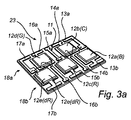
図3a〜bは、本発明の発光モジュールの2つの他の実施形態を概略的に示している。 Figures 3a-b schematically show two other embodiments of the light emitting module of the present invention.
先ず図3aを参照すると、ここに概略的に示された例となる発光モジュール23は、LED12a〜eが発光モジュール23の両側から外を向いてこれらの上側接続を伴って設けられている点と、伝導パターン11が適宜変更されている点について、図2に示された発光モジュール3bとは異なる。これにより、ボンドワイヤ接続は、コネクタ端子13a〜b,14a〜b,15a〜b,16a〜b,17a〜bから遠ざけられ、これは、glob top又は類似のもの(図3aにおいては示されない)を用いてボンドワイヤの保護を促進する一方で、glob topの塗布の後及び前にコネクタ端子13a〜b,14a〜b,15a〜b,16a〜b,17a〜bを精査することを通じて発光モジュール23の試験を依然として可能にする。
Referring first to FIG. 3a, the exemplary
図3bは、8つのLED27a〜hが3つの列28a〜cに配列される他の例となる発光モジュール26を概略的に示している。LED27a〜hは、相互に異なる原色の光を放射するように構成されたLEDの個別に制御可能なセットに設けられる。図3bに示されるように、4つのLED27a,27c,27f,27hは、緑色(G)光を放射するように構成され、2つのLED27b,27gは、青色(B)光を放射するように構成され、1つのLED27dは、赤色(R)光を放射するように構成され、1つのLED27eは、深紅色(dR)光を放射するように構成される。
FIG. 3b schematically shows another example
図3bに見られ得るように、同一色を有する光を放射するように構成された幾つかのLEDは、光源の個別に制御可能なセットを互いに一緒に形成するように接続される。図3b中の実施形態における光源の個別に制御可能なセットは、緑色(G)LED27a,27f、赤色(R)LED27d、青色(B)LED27b,27g、深紅色(dR)LED27e及び緑色(G)LED27c,27hである。
As can be seen in FIG. 3b, several LEDs configured to emit light having the same color are connected together to form an individually controllable set of light sources together. The individually controllable sets of light sources in the embodiment in FIG. 3b are green (G)
更に、図3b中の例となる発光モジュール26におけるLED27a〜hは、発光モジュール26の取り付けを促進するためにLED27a〜hに囲まれた未実装部分30が存在するように配列される。特に、ピックアンドプレースツールは、未実装部分30で発光モジュール26をピックアップし得る。
Further, the
色混合及び均一性のような斯様な因子に関する、図1中の照明デバイス1により出力された光の最適品質に関して、ここに含まれた発光デバイス2は、少なくとも相互に関連して、有利には管状反射体5にも関連して、正確に位置付けられるべきである。 Regarding the optimal quality of the light output by the lighting device 1 in FIG. 1 with respect to such factors such as color mixing and uniformity, the light-emitting device 2 included here is advantageously at least interrelated. Should be accurately positioned in relation to the tubular reflector 5 as well.
図4は、発光デバイス33a〜cの位置を規定するように構造化された熱消散構造体32を有する、本発明の一実施形態による発光デバイスを概略的に示している。発光デバイス33a〜cは、それぞれが、相互に、及び、発光デバイス33a〜cを外部電源に接続するために用いられたプリント回路基板(PCB)34に関連して、複数の内部接続された発光モジュールを有する。
FIG. 4 schematically illustrates a light emitting device according to an embodiment of the invention having a
図4に概略的に示されるように、熱消散構造体32は、発光デバイス32a〜cを収容するための多数の比較的浅い凹部35a〜cと、図4に示された例となる実施形態においては発光デバイス32a〜cよりも大幅に薄いPCB34を収容するための比較的深い凹部36とを備える。各凹部35a〜c,36に発光デバイス32a〜c及びPCB34を適合させることにより、発光デバイス32a〜cに含まれた光源は、相互に及びPCB34に関連して正確に及び確実に位置付けられ得る。
As schematically shown in FIG. 4, the
加えて、開示された実施形態に対するバリエーションは、図面、開示及び特許請求の範囲の研究から、当業者により理解され実施され得る。請求項において、"有する"という用語は、他の要素又はステップを除外するものではなく、単数表記は、複数の存在を除外するものではない。単一のプロセッサ又は他のユニットは、請求項に記載された幾つかのアイテムの機能を充足してもよい。特定の手段が相互に異なる従属請求項に記載されるという単なる事実は、これらの手段の組み合わせが有利に用いられ得ないことを示すものではない。 In addition, variations on the disclosed embodiments can be understood and implemented by those skilled in the art from a study of the drawings, the disclosure, and the claims. In the claims, the term “comprising” does not exclude other elements or steps, and the singular does not exclude a plurality. A single processor or other unit may fulfill the functions of several items recited in the claims. The mere fact that certain measures are recited in mutually different dependent claims does not indicate that a combination of these measured cannot be used to advantage.
Claims (14)
電力の供給を可能にするために前記複数の光源のうちの対応する1つの光源にそれぞれが電気的に接続された複数のコネクタ端子対とを有し、
各前記コネクタ端子対は、当該発光モジュールの両側に設けられた、第1のコネクタ端子及び第2のコネクタ端子を有し、
前記複数の光源は、当該発光モジュールの拡張の前記第1の方向に沿った予め決められた光源シーケンスで配列され、
前記複数の光源と前記複数のコネクタ端子とは、
前記対応する光源に電気的に接続された前記コネクタ端子対は、当該発光モジュールの拡張の前記第1の方向に沿った前記予め決められた光源シーケンスで配列され、
当該発光モジュールの両側のそれぞれにおける当該発光モジュールの拡張の前記第1の方向に沿った前記対応する光源の正及び負電圧への接続が空間的に交互に設けられるように、前記コネクタ端子対が配列される、
発光モジュール。 A plurality of light sources provided side by side and provided in at least first and second rows extending along a first direction of expansion of the light emitting module;
A plurality of connector terminal pairs each electrically connected to a corresponding one of the plurality of light sources to allow power supply;
Each of the connector terminal pairs has a first connector terminal and a second connector terminal provided on both sides of the light emitting module,
The plurality of light sources are arranged in a predetermined light source sequence along the first direction of expansion of the light emitting module;
The plurality of light sources and the plurality of connector terminals are:
The connector terminal pairs electrically connected to the corresponding light sources are arranged in the predetermined light source sequence along the first direction of expansion of the light emitting module ;
The connector terminal pairs are arranged in such a way that connections to the positive and negative voltages of the corresponding light sources along the first direction of the extension of the light emitting module on each side of the light emitting module are arranged alternately in space. Arranged,
Light emitting module.
前記伝導パターンは、前記複数の光源のそれぞれを、前記光源に対応する前記コネクタ端子対の前記第1のコネクタ端子及び前記第2のコネクタ端子のうち少なくとも一方と内部接続するように構成される、請求項1〜3のうちいずれか一項に記載の発光モジュール。 Having the substrate with a conductive pattern formed on the substrate;
The conductive pattern is configured to internally connect each of the plurality of light sources with at least one of the first connector terminal and the second connector terminal of the connector terminal pair corresponding to the light source. The light emitting module as described in any one of Claims 1-3.
前記光源により放射された光を受信するように構成された管状反射体とを有する、照明デバイス。 A light emitting device according to any one of claims 11 to 13 ,
And a tubular reflector configured to receive light emitted by the light source.
Applications Claiming Priority (3)
| Application Number | Priority Date | Filing Date | Title |
|---|---|---|---|
| EP09170498 | 2009-09-17 | ||
| EP09170498.1 | 2009-09-17 | ||
| PCT/IB2010/054093 WO2011033433A1 (en) | 2009-09-17 | 2010-09-10 | Light-source module and light-emitting device |
Publications (3)
| Publication Number | Publication Date |
|---|---|
| JP2013505534A JP2013505534A (en) | 2013-02-14 |
| JP2013505534A5 JP2013505534A5 (en) | 2015-02-19 |
| JP5711240B2 true JP5711240B2 (en) | 2015-04-30 |
Family
ID=43382321
Family Applications (1)
| Application Number | Title | Priority Date | Filing Date |
|---|---|---|---|
| JP2012529380A Active JP5711240B2 (en) | 2009-09-17 | 2010-09-10 | Light source module and light emitting device |
Country Status (9)
| Country | Link |
|---|---|
| US (1) | US9743521B2 (en) |
| EP (1) | EP2478750B1 (en) |
| JP (1) | JP5711240B2 (en) |
| KR (1) | KR20120081149A (en) |
| CN (1) | CN102577635B (en) |
| BR (1) | BR112012005826A2 (en) |
| CA (1) | CA2774232A1 (en) |
| RU (1) | RU2573640C2 (en) |
| WO (1) | WO2011033433A1 (en) |
Families Citing this family (6)
| Publication number | Priority date | Publication date | Assignee | Title |
|---|---|---|---|---|
| CN103148354B (en) * | 2012-09-11 | 2016-06-01 | 深圳市绎立锐光科技开发有限公司 | A kind of light-emitting device and relevant source system |
| US9559240B1 (en) | 2015-12-17 | 2017-01-31 | International Business Machines Corporation | Nano-pillar-based biosensing device |
| DE102016107495B4 (en) * | 2016-04-22 | 2022-04-14 | Tdk Electronics Ag | Multi-layer carrier system, method for producing a multi-layer carrier system and use of a multi-layer carrier system |
| DE102016107493B4 (en) * | 2016-04-22 | 2021-10-14 | Tdk Electronics Ag | Carrier system, process for its manufacture and use of the same |
| TWM539024U (en) * | 2016-12-06 | 2017-04-01 | Tzu Wang | Heat-dissipation device of lamp |
| GB201702501D0 (en) * | 2017-02-16 | 2017-04-05 | Wilkes Robert | Lighting apparatus and system |
Family Cites Families (73)
| Publication number | Priority date | Publication date | Assignee | Title |
|---|---|---|---|---|
| DE3827083A1 (en) * | 1988-08-10 | 1990-02-15 | Telefunken Electronic Gmbh | AREA SPOTLIGHT |
| US5722760A (en) | 1995-02-03 | 1998-03-03 | Chien; Tseng Lu | Electro-luminescent light assembly |
| US5827186A (en) * | 1997-04-11 | 1998-10-27 | Light Sciences Limited Partnership | Method and PDT probe for minimizing CT and MRI image artifacts |
| RU2142176C1 (en) * | 1997-06-10 | 1999-11-27 | Карпович Нина Васильевна | Light source |
| US6200002B1 (en) | 1999-03-26 | 2001-03-13 | Philips Electronics North America Corp. | Luminaire having a reflector for mixing light from a multi-color array of leds |
| DE10012734C1 (en) | 2000-03-16 | 2001-09-27 | Bjb Gmbh & Co Kg | Illumination kit for illumination, display or notice purposes has plug connector with contacts in row along edge of each light emitting module to mechanically/electrically connect modules |
| US7550935B2 (en) | 2000-04-24 | 2009-06-23 | Philips Solid-State Lighting Solutions, Inc | Methods and apparatus for downloading lighting programs |
| DE10038213A1 (en) * | 2000-08-04 | 2002-03-07 | Osram Opto Semiconductors Gmbh | Radiation source and method of making a lens mold |
| GB0030675D0 (en) | 2000-12-15 | 2001-01-31 | Rue De Int Ltd | Methods of creating high efficiency diffuse back-reflectors based on embossed surface relief |
| US6547416B2 (en) | 2000-12-21 | 2003-04-15 | Koninklijke Philips Electronics N.V. | Faceted multi-chip package to provide a beam of uniform white light from multiple monochrome LEDs |
| US6891200B2 (en) * | 2001-01-25 | 2005-05-10 | Matsushita Electric Industrial Co., Ltd. | Light-emitting unit, light-emitting unit assembly, and lighting apparatus produced using a plurality of light-emitting units |
| US7358929B2 (en) | 2001-09-17 | 2008-04-15 | Philips Solid-State Lighting Solutions, Inc. | Tile lighting methods and systems |
| US6756669B2 (en) | 2002-04-05 | 2004-06-29 | Intel Corporation | Heat spreader with down set leg attachment feature |
| US6851831B2 (en) | 2002-04-16 | 2005-02-08 | Gelcore Llc | Close packing LED assembly with versatile interconnect architecture |
| US7160002B2 (en) | 2002-06-20 | 2007-01-09 | Simon Jerome H | Segmented reflector systems and combined reflector and refractor systems |
| US6787920B2 (en) * | 2002-06-25 | 2004-09-07 | Intel Corporation | Electronic circuit board manufacturing process and associated apparatus |
| CN100421266C (en) * | 2002-08-29 | 2008-09-24 | 首尔半导体股份有限公司 | Light-emitting device having light-emitting elements |
| JP2004140185A (en) * | 2002-10-17 | 2004-05-13 | Matsushita Electric Ind Co Ltd | Light emitting device |
| CN102290409B (en) * | 2003-04-01 | 2014-01-15 | 夏普株式会社 | Light-emitting apparatus |
| US20070001177A1 (en) * | 2003-05-08 | 2007-01-04 | Koninklijke Philips Electronics N.V. | Integrated light-emitting diode system |
| EP1649514B1 (en) | 2003-07-30 | 2014-01-01 | Panasonic Corporation | Semiconductor light emitting device, light emitting module, and lighting apparatus |
| JP4046659B2 (en) | 2003-07-31 | 2008-02-13 | 日本圧着端子製造株式会社 | Memory card connector |
| US6942360B2 (en) | 2003-10-01 | 2005-09-13 | Enertron, Inc. | Methods and apparatus for an LED light engine |
| EP1586811A1 (en) | 2004-04-16 | 2005-10-19 | Koninklijke Philips Electronics N.V. | Lamps and reflector arrangement for color mixing |
| JP2005339881A (en) * | 2004-05-25 | 2005-12-08 | Hitachi Displays Ltd | Lighting device, lighting module, and liquid crystal display |
| DE102004036157B4 (en) * | 2004-07-26 | 2023-03-16 | OSRAM Opto Semiconductors Gesellschaft mit beschränkter Haftung | Electromagnetic radiation emitting optoelectronic component and light module |
| US20060044215A1 (en) | 2004-08-24 | 2006-03-02 | Brody Thomas P | Scalable tiled display assembly for forming a large-area flat-panel display by using modular display tiles |
| US7144131B2 (en) | 2004-09-29 | 2006-12-05 | Advanced Optical Technologies, Llc | Optical system using LED coupled with phosphor-doped reflective materials |
| WO2006046221A2 (en) * | 2004-10-29 | 2006-05-04 | Peter O'brien | An illuminator and manufacturing method |
| US7431489B2 (en) | 2004-11-17 | 2008-10-07 | Fusion Optix Inc. | Enhanced light fixture |
| JP4593616B2 (en) | 2005-01-25 | 2010-12-08 | 富士通株式会社 | Semiconductor device |
| US7284882B2 (en) * | 2005-02-17 | 2007-10-23 | Federal-Mogul World Wide, Inc. | LED light module assembly |
| DE202005008242U1 (en) | 2005-05-23 | 2005-09-22 | Hoffmeister Leuchten Gmbh | Electric light used as floor lighting comprises a reflector arranged in a housing close to the base with the reflector surface formed as an asymmetric sink so that light beams exit an opening in an asymmetric manner |
| US7676915B2 (en) * | 2005-09-22 | 2010-03-16 | The Artak Ter-Hovhanissian Patent Trust | Process for manufacturing an LED lamp with integrated heat sink |
| KR20070039398A (en) | 2005-10-07 | 2007-04-11 | 히다치 막셀 가부시키가이샤 | Semiconductor device, semiconductor module and semiconductor module method for producing |
| JP5080758B2 (en) * | 2005-10-07 | 2012-11-21 | 日立マクセル株式会社 | Semiconductor device |
| KR100721454B1 (en) * | 2005-11-10 | 2007-05-23 | 서울옵토디바이스주식회사 | Light emitting device for ac power operation having photonic crystal structure and method of fbbricating the same |
| US20070110386A1 (en) | 2005-11-12 | 2007-05-17 | Tien-Hon Chiang | Device having combined diffusing, collimating, and color mixing light control function |
| US7926300B2 (en) * | 2005-11-18 | 2011-04-19 | Cree, Inc. | Adaptive adjustment of light output of solid state lighting panels |
| CN101852349B (en) * | 2005-12-22 | 2012-08-29 | 松下电器产业株式会社 | Lighting apparatus with led |
| US7705365B2 (en) * | 2006-01-24 | 2010-04-27 | Denso Corporation | Lighting device and light emitting module for the same |
| TWI289947B (en) * | 2006-03-17 | 2007-11-11 | Ind Tech Res Inst | Bendable solid state planar light source, a flexible substrate therefor, and a manufacturing method therewith |
| KR100755615B1 (en) * | 2006-04-14 | 2007-09-06 | 삼성전기주식회사 | Backlight for liquid crystal display comprising light emitting diode |
| US7655957B2 (en) * | 2006-04-27 | 2010-02-02 | Cree, Inc. | Submounts for semiconductor light emitting device packages and semiconductor light emitting device packages including the same |
| US7960819B2 (en) * | 2006-07-13 | 2011-06-14 | Cree, Inc. | Leadframe-based packages for solid state emitting devices |
| EP2044364A2 (en) | 2006-07-18 | 2009-04-08 | Koninklijke Philips Electronics N.V. | Composite light source |
| KR100844757B1 (en) * | 2006-08-24 | 2008-07-07 | 엘지이노텍 주식회사 | Lighting device and display apparatus using its |
| JP2008060204A (en) | 2006-08-30 | 2008-03-13 | Nec Lcd Technologies Ltd | Led back light unit and liquid display device using the same |
| US20100224890A1 (en) * | 2006-09-18 | 2010-09-09 | Cree, Inc. | Light emitting diode chip with electrical insulation element |
| JP4306772B2 (en) * | 2006-10-05 | 2009-08-05 | 日亜化学工業株式会社 | Light emitting device |
| US7897980B2 (en) | 2006-11-09 | 2011-03-01 | Cree, Inc. | Expandable LED array interconnect |
| US10295147B2 (en) * | 2006-11-09 | 2019-05-21 | Cree, Inc. | LED array and method for fabricating same |
| EP2092798A4 (en) | 2006-12-12 | 2014-05-07 | Koninkl Philips Nv | System and method for controlling lighting |
| US8118441B2 (en) * | 2007-04-16 | 2012-02-21 | Goodrich Lighting Systems Gmbh | Color-variable LED light, particularly for lighting the interior of vehicles |
| JP2008270609A (en) | 2007-04-23 | 2008-11-06 | Harison Toshiba Lighting Corp | Heat radiating apparatus for electronic component |
| US7622795B2 (en) | 2007-05-15 | 2009-11-24 | Nichepac Technology Inc. | Light emitting diode package |
| KR100875703B1 (en) * | 2007-06-29 | 2008-12-23 | 알티전자 주식회사 | Back light unit of direct type |
| US8421093B2 (en) * | 2007-07-13 | 2013-04-16 | Rohm Co., Ltd. | LED module and LED dot matrix display |
| DE102007041193A1 (en) * | 2007-08-31 | 2009-03-05 | Osram Gesellschaft mit beschränkter Haftung | Light module for a lighting device and lighting device |
| TWI369777B (en) * | 2007-10-04 | 2012-08-01 | Young Lighting Technology Corp | Surface light source of backlight module in a flat panel display |
| KR101410496B1 (en) * | 2007-11-08 | 2014-06-20 | 삼성디스플레이 주식회사 | Light source module, back light assembly having the light source module and display apparatus having the back light assembly |
| DE102007059133B4 (en) * | 2007-12-07 | 2023-04-06 | OSRAM Opto Semiconductors Gesellschaft mit beschränkter Haftung | Substrate for an LED submount, LED submount and LED light source |
| JP5416975B2 (en) * | 2008-03-11 | 2014-02-12 | ローム株式会社 | Semiconductor light emitting device |
| USD597971S1 (en) * | 2008-03-13 | 2009-08-11 | Rohm Co., Ltd. | Light emitting diode module |
| CN101545614B (en) * | 2008-03-26 | 2012-05-23 | 富准精密工业(深圳)有限公司 | LED fixture |
| US7944708B2 (en) * | 2008-03-28 | 2011-05-17 | Chi-Hsin Lin | Structured light-emitting module for lighting apparatus |
| JP2009283776A (en) * | 2008-05-23 | 2009-12-03 | Stanley Electric Co Ltd | Semiconductor device, semiconductor device module and method for manufacturing semiconductor device module |
| DE102008031786B4 (en) * | 2008-07-04 | 2012-11-08 | Osram Ag | LED module with a heat sink |
| US9425172B2 (en) * | 2008-10-24 | 2016-08-23 | Cree, Inc. | Light emitter array |
| US8791471B2 (en) * | 2008-11-07 | 2014-07-29 | Cree Hong Kong Limited | Multi-chip light emitting diode modules |
| US7923739B2 (en) * | 2009-06-05 | 2011-04-12 | Cree, Inc. | Solid state lighting device |
| US8368112B2 (en) * | 2009-01-14 | 2013-02-05 | Cree Huizhou Opto Limited | Aligned multiple emitter package |
| US8057067B2 (en) * | 2009-05-04 | 2011-11-15 | Peterson Manufacturing Co., Inc. | Vehicle lamp with polymer conductors and mounting structures |
-
2010
- 2010-09-10 BR BR112012005826A patent/BR112012005826A2/en not_active Application Discontinuation
- 2010-09-10 JP JP2012529380A patent/JP5711240B2/en active Active
- 2010-09-10 US US13/496,539 patent/US9743521B2/en active Active
- 2010-09-10 EP EP10760076.9A patent/EP2478750B1/en active Active
- 2010-09-10 CN CN201080041630.3A patent/CN102577635B/en active Active
- 2010-09-10 CA CA2774232A patent/CA2774232A1/en not_active Abandoned
- 2010-09-10 RU RU2012115116/07A patent/RU2573640C2/en active
- 2010-09-10 WO PCT/IB2010/054093 patent/WO2011033433A1/en active Application Filing
- 2010-09-10 KR KR1020127009676A patent/KR20120081149A/en active IP Right Grant
Also Published As
| Publication number | Publication date |
|---|---|
| US20120170265A1 (en) | 2012-07-05 |
| WO2011033433A1 (en) | 2011-03-24 |
| RU2012115116A (en) | 2013-10-27 |
| RU2573640C2 (en) | 2016-01-27 |
| EP2478750A1 (en) | 2012-07-25 |
| EP2478750B1 (en) | 2014-11-12 |
| CN102577635A (en) | 2012-07-11 |
| CN102577635B (en) | 2015-03-25 |
| CA2774232A1 (en) | 2011-03-24 |
| BR112012005826A2 (en) | 2016-08-09 |
| JP2013505534A (en) | 2013-02-14 |
| KR20120081149A (en) | 2012-07-18 |
| US9743521B2 (en) | 2017-08-22 |
Similar Documents
| Publication | Publication Date | Title |
|---|---|---|
| US8492777B2 (en) | Light emitting diode package, lighting device and light emitting diode package substrate | |
| KR101662038B1 (en) | chip package | |
| JP3968226B2 (en) | Joint board for light emitting unit | |
| JP5714899B2 (en) | Solderless integrated package connector and LED for LED | |
| TWI451604B (en) | Multi-chip led devices | |
| EP1649514B1 (en) | Semiconductor light emitting device, light emitting module, and lighting apparatus | |
| JP5113349B2 (en) | RGB thermal isolation board | |
| JP5711240B2 (en) | Light source module and light emitting device | |
| JP2004172170A (en) | High luminance light emitting device and method of manufacturing the same | |
| JP2004512687A (en) | LED module | |
| KR20110118523A (en) | Lead frame for light emitting device package, light emitting device package, and illumination apparatus employing the light emitting device package | |
| JP2005158957A (en) | Light emitting device | |
| US20110309381A1 (en) | Light-emitting device and lighting apparatus | |
| JP2012004391A (en) | Light-emitting device and luminaire | |
| WO2015093180A1 (en) | Light-emitting device | |
| KR20130059871A (en) | Light emitting modul | |
| JP2014192313A (en) | LED light-emitting device | |
| JP2008508706A (en) | Light emitting diode assembly | |
| JP6811195B2 (en) | LED lighting device | |
| JP7054429B2 (en) | Light emitting device, light emitting module and its manufacturing method | |
| JP5232698B2 (en) | Manufacturing method of multi-sided substrate and semiconductor light emitting device. | |
| US8888324B2 (en) | Light-emitting device, method for assembling same and luminaire | |
| KR20090001169A (en) | Light emitting diode package and array of the same | |
| KR20140095989A (en) | Package-free and circuit board-free led device and method for fabricating the same | |
| TW201601357A (en) | Light emitting diode module package structure having thermal-electric separated function |
Legal Events
| Date | Code | Title | Description |
|---|---|---|---|
| A621 | Written request for application examination |
Free format text: JAPANESE INTERMEDIATE CODE: A621 Effective date: 20130906 |
|
| A131 | Notification of reasons for refusal |
Free format text: JAPANESE INTERMEDIATE CODE: A131 Effective date: 20140515 |
|
| RD03 | Notification of appointment of power of attorney |
Free format text: JAPANESE INTERMEDIATE CODE: A7423 Effective date: 20140612 |
|
| A521 | Request for written amendment filed |
Free format text: JAPANESE INTERMEDIATE CODE: A523 Effective date: 20140814 |
|
| A131 | Notification of reasons for refusal |
Free format text: JAPANESE INTERMEDIATE CODE: A131 Effective date: 20141010 |
|
| A524 | Written submission of copy of amendment under article 19 pct |
Free format text: JAPANESE INTERMEDIATE CODE: A524 Effective date: 20141225 |
|
| TRDD | Decision of grant or rejection written | ||
| A01 | Written decision to grant a patent or to grant a registration (utility model) |
Free format text: JAPANESE INTERMEDIATE CODE: A01 Effective date: 20150205 |
|
| A61 | First payment of annual fees (during grant procedure) |
Free format text: JAPANESE INTERMEDIATE CODE: A61 Effective date: 20150305 |
|
| R150 | Certificate of patent or registration of utility model |
Ref document number: 5711240 Country of ref document: JP Free format text: JAPANESE INTERMEDIATE CODE: R150 |
|
| S111 | Request for change of ownership or part of ownership |
Free format text: JAPANESE INTERMEDIATE CODE: R313113 |
|
| R350 | Written notification of registration of transfer |
Free format text: JAPANESE INTERMEDIATE CODE: R350 |
|
| R250 | Receipt of annual fees |
Free format text: JAPANESE INTERMEDIATE CODE: R250 |
|
| R250 | Receipt of annual fees |
Free format text: JAPANESE INTERMEDIATE CODE: R250 |
|
| S531 | Written request for registration of change of domicile |
Free format text: JAPANESE INTERMEDIATE CODE: R313531 |
|
| S533 | Written request for registration of change of name |
Free format text: JAPANESE INTERMEDIATE CODE: R313533 |
|
| R350 | Written notification of registration of transfer |
Free format text: JAPANESE INTERMEDIATE CODE: R350 |
|
| R250 | Receipt of annual fees |
Free format text: JAPANESE INTERMEDIATE CODE: R250 |
|
| R250 | Receipt of annual fees |
Free format text: JAPANESE INTERMEDIATE CODE: R250 |
|
| R250 | Receipt of annual fees |
Free format text: JAPANESE INTERMEDIATE CODE: R250 |
|
| R250 | Receipt of annual fees |
Free format text: JAPANESE INTERMEDIATE CODE: R250 |
|
| R250 | Receipt of annual fees |
Free format text: JAPANESE INTERMEDIATE CODE: R250 |