CN100401503C - Semiconductor device and manufacturing method thereof - Google Patents
Semiconductor device and manufacturing method thereof Download PDFInfo
- Publication number
- CN100401503C CN100401503C CNB2005100738045A CN200510073804A CN100401503C CN 100401503 C CN100401503 C CN 100401503C CN B2005100738045 A CNB2005100738045 A CN B2005100738045A CN 200510073804 A CN200510073804 A CN 200510073804A CN 100401503 C CN100401503 C CN 100401503C
- Authority
- CN
- China
- Prior art keywords
- semiconductor device
- semiconductor chip
- semiconductor
- wiring layer
- hole
- Prior art date
- Legal status (The legal status is an assumption and is not a legal conclusion. Google has not performed a legal analysis and makes no representation as to the accuracy of the status listed.)
- Expired - Fee Related
Links
Images


Classifications
-
- H—ELECTRICITY
- H05—ELECTRIC TECHNIQUES NOT OTHERWISE PROVIDED FOR
- H05K—PRINTED CIRCUITS; CASINGS OR CONSTRUCTIONAL DETAILS OF ELECTRIC APPARATUS; MANUFACTURE OF ASSEMBLAGES OF ELECTRICAL COMPONENTS
- H05K3/00—Apparatus or processes for manufacturing printed circuits
- H05K3/30—Assembling printed circuits with electric components, e.g. with resistors
- H05K3/32—Assembling printed circuits with electric components, e.g. with resistors electrically connecting electric components or wires to printed circuits
- H05K3/34—Assembling printed circuits with electric components, e.g. with resistors electrically connecting electric components or wires to printed circuits by soldering
- H05K3/341—Surface mounted components
- H05K3/3431—Leadless components
- H05K3/3442—Leadless components having edge contacts, e.g. leadless chip capacitors, chip carriers
-
- H—ELECTRICITY
- H10—SEMICONDUCTOR DEVICES; ELECTRIC SOLID-STATE DEVICES NOT OTHERWISE PROVIDED FOR
- H10W—GENERIC PACKAGES, INTERCONNECTIONS, CONNECTORS OR OTHER CONSTRUCTIONAL DETAILS OF DEVICES COVERED BY CLASS H10
- H10W76/00—Containers; Fillings or auxiliary members therefor; Seals
- H10W76/10—Containers or parts thereof
- H10W76/12—Containers or parts thereof characterised by their shape
- H10W76/15—Containers comprising an insulating or insulated base
- H10W76/153—Containers comprising an insulating or insulated base having interconnections in passages through the insulating or insulated base
-
- H—ELECTRICITY
- H10—SEMICONDUCTOR DEVICES; ELECTRIC SOLID-STATE DEVICES NOT OTHERWISE PROVIDED FOR
- H10D—INORGANIC ELECTRIC SEMICONDUCTOR DEVICES
- H10D62/00—Semiconductor bodies, or regions thereof, of devices having potential barriers
- H10D62/10—Shapes, relative sizes or dispositions of the regions of the semiconductor bodies; Shapes of the semiconductor bodies
- H10D62/117—Shapes of semiconductor bodies
-
- H—ELECTRICITY
- H10—SEMICONDUCTOR DEVICES; ELECTRIC SOLID-STATE DEVICES NOT OTHERWISE PROVIDED FOR
- H10P—GENERIC PROCESSES OR APPARATUS FOR THE MANUFACTURE OR TREATMENT OF DEVICES COVERED BY CLASS H10
- H10P54/00—Cutting or separating of wafers, substrates or parts of devices
-
- H—ELECTRICITY
- H10—SEMICONDUCTOR DEVICES; ELECTRIC SOLID-STATE DEVICES NOT OTHERWISE PROVIDED FOR
- H10P—GENERIC PROCESSES OR APPARATUS FOR THE MANUFACTURE OR TREATMENT OF DEVICES COVERED BY CLASS H10
- H10P72/00—Handling or holding of wafers, substrates or devices during manufacture or treatment thereof
- H10P72/70—Handling or holding of wafers, substrates or devices during manufacture or treatment thereof for supporting or gripping
- H10P72/74—Handling or holding of wafers, substrates or devices during manufacture or treatment thereof for supporting or gripping using temporarily an auxiliary support
-
- H—ELECTRICITY
- H10—SEMICONDUCTOR DEVICES; ELECTRIC SOLID-STATE DEVICES NOT OTHERWISE PROVIDED FOR
- H10W—GENERIC PACKAGES, INTERCONNECTIONS, CONNECTORS OR OTHER CONSTRUCTIONAL DETAILS OF DEVICES COVERED BY CLASS H10
- H10W20/00—Interconnections in chips, wafers or substrates
- H10W20/01—Manufacture or treatment
- H10W20/021—Manufacture or treatment of interconnections within wafers or substrates
- H10W20/023—Manufacture or treatment of interconnections within wafers or substrates the interconnections being through-semiconductor vias
- H10W20/0234—Manufacture or treatment of interconnections within wafers or substrates the interconnections being through-semiconductor vias comprising etching via holes that stop on pads or on electrodes
-
- H—ELECTRICITY
- H10—SEMICONDUCTOR DEVICES; ELECTRIC SOLID-STATE DEVICES NOT OTHERWISE PROVIDED FOR
- H10W—GENERIC PACKAGES, INTERCONNECTIONS, CONNECTORS OR OTHER CONSTRUCTIONAL DETAILS OF DEVICES COVERED BY CLASS H10
- H10W20/00—Interconnections in chips, wafers or substrates
- H10W20/01—Manufacture or treatment
- H10W20/021—Manufacture or treatment of interconnections within wafers or substrates
- H10W20/023—Manufacture or treatment of interconnections within wafers or substrates the interconnections being through-semiconductor vias
- H10W20/0242—Manufacture or treatment of interconnections within wafers or substrates the interconnections being through-semiconductor vias comprising etching via holes from the back sides of the chips, wafers or substrates
-
- H—ELECTRICITY
- H10—SEMICONDUCTOR DEVICES; ELECTRIC SOLID-STATE DEVICES NOT OTHERWISE PROVIDED FOR
- H10W—GENERIC PACKAGES, INTERCONNECTIONS, CONNECTORS OR OTHER CONSTRUCTIONAL DETAILS OF DEVICES COVERED BY CLASS H10
- H10W20/00—Interconnections in chips, wafers or substrates
- H10W20/20—Interconnections within wafers or substrates, e.g. through-silicon vias [TSV]
-
- H—ELECTRICITY
- H10—SEMICONDUCTOR DEVICES; ELECTRIC SOLID-STATE DEVICES NOT OTHERWISE PROVIDED FOR
- H10W—GENERIC PACKAGES, INTERCONNECTIONS, CONNECTORS OR OTHER CONSTRUCTIONAL DETAILS OF DEVICES COVERED BY CLASS H10
- H10W70/00—Package substrates; Interposers; Redistribution layers [RDL]
- H10W70/60—Insulating or insulated package substrates; Interposers; Redistribution layers
-
- H—ELECTRICITY
- H10—SEMICONDUCTOR DEVICES; ELECTRIC SOLID-STATE DEVICES NOT OTHERWISE PROVIDED FOR
- H10W—GENERIC PACKAGES, INTERCONNECTIONS, CONNECTORS OR OTHER CONSTRUCTIONAL DETAILS OF DEVICES COVERED BY CLASS H10
- H10W72/00—Interconnections or connectors in packages
- H10W72/01—Manufacture or treatment
- H10W72/019—Manufacture or treatment of bond pads
-
- H—ELECTRICITY
- H10—SEMICONDUCTOR DEVICES; ELECTRIC SOLID-STATE DEVICES NOT OTHERWISE PROVIDED FOR
- H10W—GENERIC PACKAGES, INTERCONNECTIONS, CONNECTORS OR OTHER CONSTRUCTIONAL DETAILS OF DEVICES COVERED BY CLASS H10
- H10W74/00—Encapsulations, e.g. protective coatings
- H10W74/01—Manufacture or treatment
-
- H—ELECTRICITY
- H05—ELECTRIC TECHNIQUES NOT OTHERWISE PROVIDED FOR
- H05K—PRINTED CIRCUITS; CASINGS OR CONSTRUCTIONAL DETAILS OF ELECTRIC APPARATUS; MANUFACTURE OF ASSEMBLAGES OF ELECTRICAL COMPONENTS
- H05K2201/00—Indexing scheme relating to printed circuits covered by H05K1/00
- H05K2201/03—Conductive materials
- H05K2201/0332—Structure of the conductor
- H05K2201/0364—Conductor shape
- H05K2201/0367—Metallic bump or raised conductor not used as solder bump
-
- H—ELECTRICITY
- H05—ELECTRIC TECHNIQUES NOT OTHERWISE PROVIDED FOR
- H05K—PRINTED CIRCUITS; CASINGS OR CONSTRUCTIONAL DETAILS OF ELECTRIC APPARATUS; MANUFACTURE OF ASSEMBLAGES OF ELECTRICAL COMPONENTS
- H05K2201/00—Indexing scheme relating to printed circuits covered by H05K1/00
- H05K2201/09—Shape and layout
- H05K2201/09145—Edge details
- H05K2201/09154—Bevelled, chamferred or tapered edge
-
- H—ELECTRICITY
- H05—ELECTRIC TECHNIQUES NOT OTHERWISE PROVIDED FOR
- H05K—PRINTED CIRCUITS; CASINGS OR CONSTRUCTIONAL DETAILS OF ELECTRIC APPARATUS; MANUFACTURE OF ASSEMBLAGES OF ELECTRICAL COMPONENTS
- H05K2201/00—Indexing scheme relating to printed circuits covered by H05K1/00
- H05K2201/20—Details of printed circuits not provided for in H05K2201/01 - H05K2201/10
- H05K2201/2036—Permanent spacer or stand-off in a printed circuit or printed circuit assembly
-
- H—ELECTRICITY
- H10—SEMICONDUCTOR DEVICES; ELECTRIC SOLID-STATE DEVICES NOT OTHERWISE PROVIDED FOR
- H10P—GENERIC PROCESSES OR APPARATUS FOR THE MANUFACTURE OR TREATMENT OF DEVICES COVERED BY CLASS H10
- H10P72/00—Handling or holding of wafers, substrates or devices during manufacture or treatment thereof
- H10P72/70—Handling or holding of wafers, substrates or devices during manufacture or treatment thereof for supporting or gripping
- H10P72/74—Handling or holding of wafers, substrates or devices during manufacture or treatment thereof for supporting or gripping using temporarily an auxiliary support
- H10P72/7422—Handling or holding of wafers, substrates or devices during manufacture or treatment thereof for supporting or gripping using temporarily an auxiliary support used to protect an active side of a device or wafer
-
- H—ELECTRICITY
- H10—SEMICONDUCTOR DEVICES; ELECTRIC SOLID-STATE DEVICES NOT OTHERWISE PROVIDED FOR
- H10W—GENERIC PACKAGES, INTERCONNECTIONS, CONNECTORS OR OTHER CONSTRUCTIONAL DETAILS OF DEVICES COVERED BY CLASS H10
- H10W70/00—Package substrates; Interposers; Redistribution layers [RDL]
- H10W70/60—Insulating or insulated package substrates; Interposers; Redistribution layers
- H10W70/62—Insulating or insulated package substrates; Interposers; Redistribution layers characterised by their interconnections
- H10W70/65—Shapes or dispositions of interconnections
- H10W70/654—Top-view layouts
- H10W70/656—Fan-in layouts
-
- H—ELECTRICITY
- H10—SEMICONDUCTOR DEVICES; ELECTRIC SOLID-STATE DEVICES NOT OTHERWISE PROVIDED FOR
- H10W—GENERIC PACKAGES, INTERCONNECTIONS, CONNECTORS OR OTHER CONSTRUCTIONAL DETAILS OF DEVICES COVERED BY CLASS H10
- H10W72/00—Interconnections or connectors in packages
- H10W72/01—Manufacture or treatment
- H10W72/012—Manufacture or treatment of bump connectors, dummy bumps or thermal bumps
-
- H—ELECTRICITY
- H10—SEMICONDUCTOR DEVICES; ELECTRIC SOLID-STATE DEVICES NOT OTHERWISE PROVIDED FOR
- H10W—GENERIC PACKAGES, INTERCONNECTIONS, CONNECTORS OR OTHER CONSTRUCTIONAL DETAILS OF DEVICES COVERED BY CLASS H10
- H10W72/00—Interconnections or connectors in packages
- H10W72/01—Manufacture or treatment
- H10W72/0198—Manufacture or treatment batch processes
-
- H—ELECTRICITY
- H10—SEMICONDUCTOR DEVICES; ELECTRIC SOLID-STATE DEVICES NOT OTHERWISE PROVIDED FOR
- H10W—GENERIC PACKAGES, INTERCONNECTIONS, CONNECTORS OR OTHER CONSTRUCTIONAL DETAILS OF DEVICES COVERED BY CLASS H10
- H10W72/00—Interconnections or connectors in packages
- H10W72/071—Connecting or disconnecting
- H10W72/072—Connecting or disconnecting of bump connectors
- H10W72/07231—Techniques
- H10W72/07234—Using a reflow oven
-
- H—ELECTRICITY
- H10—SEMICONDUCTOR DEVICES; ELECTRIC SOLID-STATE DEVICES NOT OTHERWISE PROVIDED FOR
- H10W—GENERIC PACKAGES, INTERCONNECTIONS, CONNECTORS OR OTHER CONSTRUCTIONAL DETAILS OF DEVICES COVERED BY CLASS H10
- H10W72/00—Interconnections or connectors in packages
- H10W72/071—Connecting or disconnecting
- H10W72/072—Connecting or disconnecting of bump connectors
- H10W72/07231—Techniques
- H10W72/07236—Soldering or alloying
-
- H—ELECTRICITY
- H10—SEMICONDUCTOR DEVICES; ELECTRIC SOLID-STATE DEVICES NOT OTHERWISE PROVIDED FOR
- H10W—GENERIC PACKAGES, INTERCONNECTIONS, CONNECTORS OR OTHER CONSTRUCTIONAL DETAILS OF DEVICES COVERED BY CLASS H10
- H10W72/00—Interconnections or connectors in packages
- H10W72/071—Connecting or disconnecting
- H10W72/072—Connecting or disconnecting of bump connectors
- H10W72/07251—Connecting or disconnecting of bump connectors characterised by changes in properties of the bump connectors during connecting
- H10W72/07254—Connecting or disconnecting of bump connectors characterised by changes in properties of the bump connectors during connecting changes in dispositions
-
- H—ELECTRICITY
- H10—SEMICONDUCTOR DEVICES; ELECTRIC SOLID-STATE DEVICES NOT OTHERWISE PROVIDED FOR
- H10W—GENERIC PACKAGES, INTERCONNECTIONS, CONNECTORS OR OTHER CONSTRUCTIONAL DETAILS OF DEVICES COVERED BY CLASS H10
- H10W72/00—Interconnections or connectors in packages
- H10W72/071—Connecting or disconnecting
- H10W72/074—Connecting or disconnecting of anisotropic conductive adhesives
-
- H—ELECTRICITY
- H10—SEMICONDUCTOR DEVICES; ELECTRIC SOLID-STATE DEVICES NOT OTHERWISE PROVIDED FOR
- H10W—GENERIC PACKAGES, INTERCONNECTIONS, CONNECTORS OR OTHER CONSTRUCTIONAL DETAILS OF DEVICES COVERED BY CLASS H10
- H10W72/00—Interconnections or connectors in packages
- H10W72/20—Bump connectors, e.g. solder bumps or copper pillars; Dummy bumps; Thermal bumps
- H10W72/241—Dispositions, e.g. layouts
- H10W72/242—Dispositions, e.g. layouts relative to the surface, e.g. recessed, protruding
-
- H—ELECTRICITY
- H10—SEMICONDUCTOR DEVICES; ELECTRIC SOLID-STATE DEVICES NOT OTHERWISE PROVIDED FOR
- H10W—GENERIC PACKAGES, INTERCONNECTIONS, CONNECTORS OR OTHER CONSTRUCTIONAL DETAILS OF DEVICES COVERED BY CLASS H10
- H10W72/00—Interconnections or connectors in packages
- H10W72/20—Bump connectors, e.g. solder bumps or copper pillars; Dummy bumps; Thermal bumps
- H10W72/241—Dispositions, e.g. layouts
- H10W72/244—Dispositions, e.g. layouts relative to underlying supporting features, e.g. bond pads, RDLs or vias
-
- H—ELECTRICITY
- H10—SEMICONDUCTOR DEVICES; ELECTRIC SOLID-STATE DEVICES NOT OTHERWISE PROVIDED FOR
- H10W—GENERIC PACKAGES, INTERCONNECTIONS, CONNECTORS OR OTHER CONSTRUCTIONAL DETAILS OF DEVICES COVERED BY CLASS H10
- H10W72/00—Interconnections or connectors in packages
- H10W72/20—Bump connectors, e.g. solder bumps or copper pillars; Dummy bumps; Thermal bumps
- H10W72/251—Materials
-
- H—ELECTRICITY
- H10—SEMICONDUCTOR DEVICES; ELECTRIC SOLID-STATE DEVICES NOT OTHERWISE PROVIDED FOR
- H10W—GENERIC PACKAGES, INTERCONNECTIONS, CONNECTORS OR OTHER CONSTRUCTIONAL DETAILS OF DEVICES COVERED BY CLASS H10
- H10W72/00—Interconnections or connectors in packages
- H10W72/20—Bump connectors, e.g. solder bumps or copper pillars; Dummy bumps; Thermal bumps
- H10W72/29—Bond pads specially adapted therefor
-
- H—ELECTRICITY
- H10—SEMICONDUCTOR DEVICES; ELECTRIC SOLID-STATE DEVICES NOT OTHERWISE PROVIDED FOR
- H10W—GENERIC PACKAGES, INTERCONNECTIONS, CONNECTORS OR OTHER CONSTRUCTIONAL DETAILS OF DEVICES COVERED BY CLASS H10
- H10W72/00—Interconnections or connectors in packages
- H10W72/30—Die-attach connectors
- H10W72/351—Materials of die-attach connectors
- H10W72/353—Materials of die-attach connectors not comprising solid metals or solid metalloids, e.g. ceramics
- H10W72/354—Materials of die-attach connectors not comprising solid metals or solid metalloids, e.g. ceramics comprising polymers
-
- H—ELECTRICITY
- H10—SEMICONDUCTOR DEVICES; ELECTRIC SOLID-STATE DEVICES NOT OTHERWISE PROVIDED FOR
- H10W—GENERIC PACKAGES, INTERCONNECTIONS, CONNECTORS OR OTHER CONSTRUCTIONAL DETAILS OF DEVICES COVERED BY CLASS H10
- H10W72/00—Interconnections or connectors in packages
- H10W72/90—Bond pads, in general
- H10W72/921—Structures or relative sizes of bond pads
- H10W72/922—Bond pads being integral with underlying chip-level interconnections
-
- H—ELECTRICITY
- H10—SEMICONDUCTOR DEVICES; ELECTRIC SOLID-STATE DEVICES NOT OTHERWISE PROVIDED FOR
- H10W—GENERIC PACKAGES, INTERCONNECTIONS, CONNECTORS OR OTHER CONSTRUCTIONAL DETAILS OF DEVICES COVERED BY CLASS H10
- H10W72/00—Interconnections or connectors in packages
- H10W72/90—Bond pads, in general
- H10W72/921—Structures or relative sizes of bond pads
- H10W72/923—Bond pads having multiple stacked layers
-
- H—ELECTRICITY
- H10—SEMICONDUCTOR DEVICES; ELECTRIC SOLID-STATE DEVICES NOT OTHERWISE PROVIDED FOR
- H10W—GENERIC PACKAGES, INTERCONNECTIONS, CONNECTORS OR OTHER CONSTRUCTIONAL DETAILS OF DEVICES COVERED BY CLASS H10
- H10W72/00—Interconnections or connectors in packages
- H10W72/90—Bond pads, in general
- H10W72/941—Dispositions of bond pads
- H10W72/9415—Dispositions of bond pads relative to the surface, e.g. recessed, protruding
-
- H—ELECTRICITY
- H10—SEMICONDUCTOR DEVICES; ELECTRIC SOLID-STATE DEVICES NOT OTHERWISE PROVIDED FOR
- H10W—GENERIC PACKAGES, INTERCONNECTIONS, CONNECTORS OR OTHER CONSTRUCTIONAL DETAILS OF DEVICES COVERED BY CLASS H10
- H10W72/00—Interconnections or connectors in packages
- H10W72/90—Bond pads, in general
- H10W72/951—Materials of bond pads
- H10W72/952—Materials of bond pads comprising metals or metalloids, e.g. PbSn, Ag or Cu
-
- H—ELECTRICITY
- H10—SEMICONDUCTOR DEVICES; ELECTRIC SOLID-STATE DEVICES NOT OTHERWISE PROVIDED FOR
- H10W—GENERIC PACKAGES, INTERCONNECTIONS, CONNECTORS OR OTHER CONSTRUCTIONAL DETAILS OF DEVICES COVERED BY CLASS H10
- H10W74/00—Encapsulations, e.g. protective coatings
- H10W74/10—Encapsulations, e.g. protective coatings characterised by their shape or disposition
- H10W74/111—Encapsulations, e.g. protective coatings characterised by their shape or disposition the semiconductor body being completely enclosed
- H10W74/129—Encapsulations, e.g. protective coatings characterised by their shape or disposition the semiconductor body being completely enclosed forming a chip-scale package [CSP]
-
- Y—GENERAL TAGGING OF NEW TECHNOLOGICAL DEVELOPMENTS; GENERAL TAGGING OF CROSS-SECTIONAL TECHNOLOGIES SPANNING OVER SEVERAL SECTIONS OF THE IPC; TECHNICAL SUBJECTS COVERED BY FORMER USPC CROSS-REFERENCE ART COLLECTIONS [XRACs] AND DIGESTS
- Y02—TECHNOLOGIES OR APPLICATIONS FOR MITIGATION OR ADAPTATION AGAINST CLIMATE CHANGE
- Y02P—CLIMATE CHANGE MITIGATION TECHNOLOGIES IN THE PRODUCTION OR PROCESSING OF GOODS
- Y02P70/00—Climate change mitigation technologies in the production process for final industrial or consumer products
- Y02P70/50—Manufacturing or production processes characterised by the final manufactured product
Landscapes
- Engineering & Computer Science (AREA)
- Manufacturing & Machinery (AREA)
- Microelectronics & Electronic Packaging (AREA)
- Internal Circuitry In Semiconductor Integrated Circuit Devices (AREA)
Abstract
一种半导体装置及其制造方法,可不使工序复杂,提高安装时的强度及精度。在半导体衬底(10)的背面沿切割线(DL)形成槽(14)。进而形成从半导体衬底(10)的背面到达焊盘电极(11)的通孔(16)。在通孔(16)内形成埋入电极(18),和其连接,形成沿切割线(DL)附近延伸的配线层(19)。在配线层(19)的端部形成导电端子(21)。然后,通过进行沿切割线(DL)的切割,完成在背面端部具有倾斜面1s的半导体装置(1)。在半导体装置(1)通过回流处理与电路衬底(30)连接时,流动性增强的导电膏覆盖导电端子(21)及倾斜面(1s)。在此,在半导体装置(1)外缘的电路衬底(30)上形成含有侧嵌条的导电膏(40a、40b)。
A semiconductor device and its manufacturing method can improve the strength and precision of mounting without complicating the process. Grooves (14) are formed along dicing lines (DL) on the back surface of a semiconductor substrate (10). Further, a through hole (16) reaching the pad electrode (11) from the back surface of the semiconductor substrate (10) is formed. A buried electrode (18) is formed in the through hole (16) and connected thereto to form a wiring layer (19) extending near the dicing line (DL). Conductive terminals (21) are formed at the ends of the wiring layer (19). Then, by performing dicing along the dicing line (DL), the semiconductor device ( 1 ) having the inclined surface 1 s at the end portion of the rear surface is completed. When the semiconductor device (1) is connected to the circuit substrate (30) through reflow treatment, the conductive paste with enhanced fluidity covers the conductive terminal (21) and the inclined surface (1s). Here, conductive paste (40a, 40b) including side fillets is formed on a circuit substrate (30) on the outer edge of a semiconductor device (1).
Description
技术领域 technical field
本发明涉及半导体装置及其制造方法,特别是涉及封装型半导体装置及其制造方法。The present invention relates to a semiconductor device and a manufacturing method thereof, and particularly relates to a packaged semiconductor device and a manufacturing method thereof.
背景技术 Background technique
近年来,作为封装型半导体装置,CSP(芯片尺寸封装Chip Size Package)受到人们的关注。CSP是具有和半导体芯片的外形尺寸大致相同尺寸的外形尺寸的小型封装。In recent years, CSP (Chip Size Package) has attracted attention as a packaged semiconductor device. A CSP is a small package having an outer dimension approximately the same as that of a semiconductor chip.
目前,CSP的一种,可知有BGA(焊球阵列Ball GridArray)型半导体装置。该BGA型半导体装置中,在封装的一主面上格子状地排列多个由焊锡等金属部件构成的球状导电端子,并将其与搭载于封装的其它主面上的半导体芯片电连接。下面,参照附图说明现有例的BGA型半导体装置。Currently, as one type of CSP, a BGA (Ball Grid Array) type semiconductor device is known. In this BGA type semiconductor device, a plurality of spherical conductive terminals made of metal members such as solder are arranged in a grid on one main surface of a package, and are electrically connected to a semiconductor chip mounted on the other main surface of the package. Next, a conventional BGA type semiconductor device will be described with reference to the drawings.
图9是说明现有例的半导体装置的剖面图。如图9所示,在半导体装置2的半导体芯片60A的表面形成有焊盘电极61。另外,半导体芯片60A的表面被密封件63(或支承体)覆盖。在半导体芯片60A上形成有从该背面贯通到焊盘电极61的通孔。在该通孔中形成有和焊盘电极61连接的埋入电极68。在半导体芯片60A背面的通孔露出的埋入电极68上形成有球状的导电端子71。FIG. 9 is a cross-sectional view illustrating a conventional semiconductor device. As shown in FIG. 9 , a pad electrode 61 is formed on the surface of the semiconductor chip 60A of the semiconductor device 2 . In addition, the surface of the semiconductor chip 60A is covered with a sealing member 63 (or a support body). A via hole penetrating from the back surface to the pad electrode 61 is formed in the semiconductor chip 60A. A buried electrode 68 connected to the pad electrode 61 is formed in the via hole. Ball-shaped conductive terminals 71 are formed on the buried electrodes 68 exposed through the through holes on the back surface of the semiconductor chip 60A.
该半导体装置2在安装于形成有未图示的导电图案的电路衬底80上时,使电路衬底80和半导体芯片的背面对向,设置在该电路衬底80上。在此,在形成有未图示的导电图案的电路衬底80的主面上,在和导电端子71接触的位置利用例如印刷法形成有由例如焊锡构成的导电膏90。另外,在电路衬底80的主面上,在不形成导电膏90的区域形成有用于防止在半导体芯片60A的背面和电路衬底80之间产生空间的所谓的底层填料91。When the semiconductor device 2 is mounted on a circuit substrate 80 on which a conductive pattern (not shown) is formed, the circuit substrate 80 and the back surface of the semiconductor chip are placed on the circuit substrate 80 facing each other. Here, conductive paste 90 made of, for example, solder is formed on the main surface of circuit board 80 on which a not-shown conductive pattern is formed, at positions in contact with conductive terminals 71 by, for example, printing. Also, on the main surface of the circuit substrate 80 , a so-called underfill 91 for preventing a space between the back surface of the semiconductor chip 60A and the circuit substrate 80 is formed in a region where the conductive paste 90 is not formed.
导电膏90通过回流处理增加流动性,部分地覆盖导电端子71。由此,导电端子71和电路衬底80的未图示的导电图案电连接,同时,固定在电路衬底80上。The conductive paste 90 increases fluidity through the reflow process, and partially covers the conductive terminals 71 . Accordingly, the conductive terminal 71 is electrically connected to the not-shown conductive pattern of the circuit substrate 80 and is fixed to the circuit substrate 80 at the same time.
另外,关联的技术文献可举出例如以下的专利文献。In addition, related technical documents include, for example, the following patent documents.
专利文献1:特开2003-309221号公报Patent Document 1: JP-A-2003-309221
专利文献2:特表2002-512436号公报Patent Document 2: Special Publication No. 2002-512436
专利文献3:特开2003-229518号公报Patent Document 3: JP-A-2003-229518
但是,在介由导电膏90连接上述的现有例的半导体装置2和电路衬底80时,存在产生连接不良的问题。这是由于,形成于电路衬底80上的导电膏90的量被限制为少量,故有时在回流处理时,导电膏90不能准确地流到导电端子71和电路衬底80的未图示的导电图案两者上。另外,在为解决上述连接不良而增加导电膏90的量时,产生了回流处理时多于的导电膏使相邻的导电端子71短路这样的问题。另外,难于确认是否正确地连接着。However, when the semiconductor device 2 of the conventional example described above and the circuit board 80 are connected through the conductive paste 90 , there is a problem that poor connection occurs. This is because the amount of the conductive paste 90 formed on the circuit substrate 80 is limited to a small amount, so sometimes the conductive paste 90 cannot accurately flow to the conductive terminals 71 and the unillustrated parts of the circuit substrate 80 during the reflow process. conductive patterns on both. In addition, when the amount of conductive paste 90 is increased to solve the above-mentioned poor connection, there arises a problem that adjacent conductive terminals 71 are short-circuited by the excess conductive paste during reflow processing. In addition, it is difficult to confirm whether it is connected correctly.
另外,即使介由导电膏90将半导体装置2和电路衬底80正确地连接,但由于导电膏的量少,故连接时的机械强度也不够。因此,在半导体芯片60A和电路衬底80之间形成所谓的由环氧树脂等构成的底层填料,抑制导电端子71间的短路,同时,加强上述机械强度。该底层填料的形成通常由半导体装置的用户进行,故存在用户进行安装时的工序增加这样的问题。Also, even if the semiconductor device 2 and the circuit board 80 are correctly connected via the conductive paste 90, the mechanical strength at the time of connection is insufficient because the amount of the conductive paste is small. Therefore, a so-called underfill made of epoxy resin or the like is formed between the semiconductor chip 60A and the circuit substrate 80 to suppress a short circuit between the conductive terminals 71 and at the same time enhance the above-mentioned mechanical strength. The formation of the underfill is usually performed by the user of the semiconductor device, so there is a problem that the number of steps required for mounting by the user increases.
结果是,半导体装置的用户安装时的工序复杂,且安装时的精度降低。因此,本发明提供一种半导体装置及其制造方法,其不会使工序复杂,且可提高安装时的强度及精度。As a result, the process of mounting by the user of the semiconductor device is complicated, and the accuracy of mounting is lowered. Therefore, the present invention provides a semiconductor device and its manufacturing method, which can improve the strength and precision of mounting without complicating the process.
发明内容 Contents of the invention
本发明的半导体装置是鉴于上述课题而开发的,其提供一种半导体装置,载置于电路衬底上,具有以下特征。The semiconductor device of the present invention has been developed in view of the above problems, and provides a semiconductor device mounted on a circuit substrate, which has the following characteristics.
即,本发明的半导体装置包括:半导体芯片;焊盘电极,其形成于半导体芯片的表面上;倾斜面,其从半导体芯片的背面的端部倾斜到该半导体芯片的侧面;通孔,其从半导体芯片的背面贯通到焊盘电极的表面;绝缘膜,其形成于含有通孔的侧壁的半导体芯片的背面上;埋入电极,其经由绝缘膜形成于通孔中,且和焊盘电极电连接;配线层,其经由绝缘膜形成在含通孔在内的半导体芯片的背面上,和埋入电极连接,且在半导体芯片的倾斜面上延伸。在此,半导体装置使电路衬底和半导体芯片的背面相对而载置于电路衬底上。另外,本发明的半导体装置在上述结构的基础上,具有形成于配线层上的导电端子。That is, the semiconductor device of the present invention includes: a semiconductor chip; a pad electrode, which is formed on the surface of the semiconductor chip; an inclined surface, which is inclined from the end of the back surface of the semiconductor chip to the side surface of the semiconductor chip; The back surface of the semiconductor chip is penetrated to the surface of the pad electrode; the insulating film is formed on the back surface of the semiconductor chip including the side wall of the through hole; the buried electrode is formed in the through hole through the insulating film, and is connected with the pad electrode Electrical connection; a wiring layer that is formed on the back surface of the semiconductor chip including through holes through an insulating film, is connected to the buried electrode, and extends on the inclined surface of the semiconductor chip. Here, the semiconductor device is placed on the circuit substrate so that the circuit substrate and the back surface of the semiconductor chip face each other. In addition, the semiconductor device of the present invention has the conductive terminals formed on the wiring layer in addition to the above configuration.
本发明的半导体装置在上述结构的基础上,在半导体芯片背面的端部形成有覆盖埋入电极上及所述倾斜面上的配线层(在形成导电端子时包括导电端子)的导电性嵌条。另外,本发明的半导体装置在上述结构的基础上,在半导体芯片的表面上形成有支承体。In the semiconductor device of the present invention, in addition to the above structure, a conductive embedding layer covering the wiring layer (including the conductive terminal when forming the conductive terminal) on the buried electrode and the inclined surface is formed at the end of the back surface of the semiconductor chip. strip. In addition, in the semiconductor device of the present invention, in addition to the above configuration, the support body is formed on the surface of the semiconductor chip.
本发明提供一种半导体装置的制造方法,其特征在于,包括:准备由切割线区分,且在表面上形成焊盘电极的半导体衬底,在半导体衬底的背面,沿切割线形成向半导体衬底的表面方向成尖头的槽的工序;形成从所述半导体衬底的背面到达所述半导体衬底的所述焊盘电极侧表面的通孔的工序;在槽内和所述通孔的侧壁以及除所述通孔外的半导体衬底的背面形成绝缘膜的工序;形成经由所述绝缘膜设置在所述通孔中并和焊盘电极电连接的埋入电极的工序;形成经由所述绝缘膜配置在含所述通孔在内的所述半导体芯片的背面上、和埋入电极连接且延伸到切割线附近的配线层的工序;通过沿切割线进行切割,将半导体衬底分割成多个半导体芯片的工序。另外,本发明的半导体装置的制造方法在上述工序的基础上,具有在配线层上形成导电端子的工序。The invention provides a manufacturing method of a semiconductor device, which is characterized in that it includes: preparing a semiconductor substrate that is distinguished by a cutting line and forming a pad electrode on the surface; The process of forming a groove with a sharp tip in the direction of the bottom surface; the process of forming a through hole reaching from the back surface of the semiconductor substrate to the side surface of the pad electrode of the semiconductor substrate; in the groove and the through hole A step of forming an insulating film on the side wall and the back surface of the semiconductor substrate except the through hole; a step of forming a buried electrode provided in the through hole through the insulating film and electrically connected to the pad electrode; The process of disposing the insulating film on the back surface of the semiconductor chip including the through hole, connecting to the buried electrode and extending to the wiring layer near the dicing line; by dicing along the dicing line, the semiconductor substrate is The process of dividing the bottom into multiple semiconductor chips. In addition, the method of manufacturing a semiconductor device according to the present invention includes a step of forming a conductive terminal on the wiring layer in addition to the above-mentioned steps.
本发明的半导体装置的制造方法在上述工序的基础上,具有在半导体芯片的背面的端部形成覆盖埋入电极上及倾斜面上的配线层(在形成导电端子时包括导电端子)的导电性嵌条的工序。另外,本发明的半导体装置的制造方法在上述工序的基础上,具有在半导体芯片的表面上形成支承体的工序。The manufacturing method of the semiconductor device of the present invention, on the basis of the above steps, has a conductive method of forming a wiring layer covering the buried electrode and the inclined surface (including the conductive terminal when forming the conductive terminal) at the end of the back surface of the semiconductor chip. Sexual molding process. In addition, the method of manufacturing a semiconductor device according to the present invention includes the step of forming a support on the surface of the semiconductor chip in addition to the above-mentioned steps.
根据本发明,在将半导体装置安装在电路衬底上时,利用回流处理增加流动性的导电膏利用形成于半导体装置背面的倾斜面的表面张力沿该倾斜面朝向半导体芯片表面的方向流动,同时,沿电路衬底朝向半导体芯片的外部流动。由此,不仅导电端子,连半导体装置的背面的倾斜面也由导电膏覆盖。因此,可最大限度地抑制现有例中所见的导电端子和电路衬底的连接不良。另外,可提高将半导体装置连接到电路衬底上时的机械强度。According to the present invention, when the semiconductor device is mounted on the circuit substrate, the conductive paste whose fluidity is increased by the reflow process utilizes the surface tension of the inclined surface formed on the back surface of the semiconductor device to flow along the inclined surface toward the surface of the semiconductor chip, and at the same time , flows along the circuit substrate toward the outside of the semiconductor chip. Accordingly, not only the conductive terminals but also the inclined surface on the back surface of the semiconductor device are covered with the conductive paste. Therefore, poor connection between the conductive terminal and the circuit substrate, which has been seen in conventional examples, can be suppressed as much as possible. In addition, the mechanical strength at the time of connecting the semiconductor device to the circuit substrate can be improved.
在正确地进行了所述连接时,从半导体装置的表面来看,存在从半导体装置的侧面溢出的导电膏(所谓的侧嵌条)。因此,进行上述连接的半导体装置的用户可通过观察该侧嵌条的有无,确认是否正确地进行了上述连接。When the connection is correctly performed, there is conductive paste (so-called side fillet) overflowing from the side of the semiconductor device when viewed from the surface of the semiconductor device. Therefore, the user of the semiconductor device performing the above-mentioned connection can check whether the above-mentioned connection is correctly made by observing the presence or absence of the side fillet.
另外,由于所述倾斜面的表面张力,导电膏具有沿电路衬底朝向半导体装置外部流动的倾向,故与现有例相比,即使在电路衬底上形成大量的导电膏,也可以最大限度地抑制导电膏埋入相邻的导电端子间的空间。即,可最大限度地抑制导电端子间短路。In addition, due to the surface tension of the inclined surface, the conductive paste tends to flow along the circuit substrate toward the outside of the semiconductor device. Therefore, compared with the conventional example, even if a large amount of conductive paste is formed on the circuit substrate, it can be used to the maximum extent. ground suppresses the conductive paste from being buried in the spaces between adjacent conductive terminals. That is, short circuit between conductive terminals can be suppressed as much as possible.
另外,由于可提高将半导体装置与电路衬底连接时的机械强度,且最大限度地避免导电端子间的短路,故可省略现有例所见的半导体装置的用户进行的底层填料的形成工序。In addition, since the mechanical strength at the time of connecting the semiconductor device to the circuit substrate can be improved, and the short circuit between the conductive terminals can be avoided as much as possible, it is possible to omit the formation process of the underfill by the user of the semiconductor device seen in the conventional example.
结果是,可不使工序复杂而提高安装时的强度及精度。As a result, the strength and precision at the time of mounting can be improved without complicating the process.
附图说明 Description of drawings
图1是表示本发明实施例的半导体装置的制造方法的剖面图;1 is a cross-sectional view showing a method of manufacturing a semiconductor device according to an embodiment of the present invention;
图2是表示本发明实施例的半导体装置的制造方法的剖面图;2 is a cross-sectional view showing a method of manufacturing a semiconductor device according to an embodiment of the present invention;
图3是表示本发明实施例的半导体装置的制造方法的剖面图;3 is a cross-sectional view showing a method of manufacturing a semiconductor device according to an embodiment of the present invention;
图4是表示本发明实施例的半导体装置的制造方法的剖面图;4 is a cross-sectional view showing a method of manufacturing a semiconductor device according to an embodiment of the present invention;
图5是表示本发明实施例的半导体装置的制造方法的剖面图;5 is a cross-sectional view showing a method of manufacturing a semiconductor device according to an embodiment of the present invention;
图6是表示本发明实施例的半导体装置及其制造方法的剖面图;6 is a cross-sectional view showing a semiconductor device and a manufacturing method thereof according to an embodiment of the present invention;
图7是说明本发明实施例的半导体装置的剖面图;7 is a cross-sectional view illustrating a semiconductor device according to an embodiment of the present invention;
图8是说明本发明实施例的半导体装置的剖面图;8 is a cross-sectional view illustrating a semiconductor device according to an embodiment of the present invention;
图9是说明现有例的半导体装置的剖面图。FIG. 9 is a cross-sectional view illustrating a conventional semiconductor device.
具体实施方式 Detailed ways
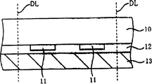
下面,参照附图详细说明本实施例的半导体装置的制造方法。图1~图5是表示本实施例的半导体装置的制造方法的剖面图。图6是表示本实施例的半导体装置及其制造方法的剖面图。图1~图6中表示构成半导体装置的半导体衬底中切割线DL附近。Next, a method of manufacturing a semiconductor device according to this embodiment will be described in detail with reference to the drawings. 1 to 5 are cross-sectional views showing a method of manufacturing a semiconductor device according to this embodiment. FIG. 6 is a cross-sectional view showing the semiconductor device and its manufacturing method of the present embodiment. 1 to 6 show the vicinity of the dicing line DL in the semiconductor substrate constituting the semiconductor device.
首先,如图1所示,准备形成有未图示的电子器件的半导体衬底10。未图示的电子器件形成于半导体衬底10的第一主面即表面上。在此,在半导体衬底10的表面介由来图示的绝缘膜形成有从未图示的电子器件延伸的焊盘电极11。另外,焊盘电极11的个数不限于图2所示的个数(2个)。另外,在上述半导体衬底10上,在使上述焊盘电极11的局部露出的状态下,形成有由氧化硅膜或氮化硅膜构成的未图示的钝化膜。First, as shown in FIG. 1 , a
在包括未图示的电子器件上及焊盘电极11上的半导体衬底10的表面上,覆盖它们而形成例如由环氧树脂等构成的树脂层12。另外,在半导体衬底10的表面上介由树脂层12形成支承体13。在形成于该表面上的未图示的电子器件为受光元件时,支承体13使用具有透明或半透明性状的材料、衬底、树脂或带等。在未图示的电子器件不是受光元件时,支承体13不限于透明或半透明性状。另外,该支承体13的形成根据未图示的电子器件或半导体装置的使用目的也可以省略。A
其次,根据需要,研磨半导体衬底10的背面直至规定的厚度。即进行背面研磨。另外,也可以蚀刻该背面,除去由背面研磨产生的机械性损伤层。Next, if necessary, the back surface of the
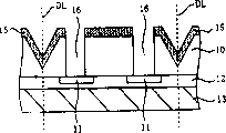
其次,如图2所示,沿切割线DL在半导体衬底10的背面上形成槽14。该槽14通过例如使用切割片进行的切削形成。在此,槽14具有相对于半导体衬底10的背面以规定角度倾斜的倾斜面。该倾斜面从半导体衬底10的背面朝向该表面形成,汇聚于切割线DL。Next, as shown in FIG. 2,
其次,如图3所示,在半导体衬底10的背面上选择性地形成第一抗蚀层15。即,第一抗蚀层15在对应焊盘电极11的规定位置具有开口部。然后,以第一抗蚀层15为掩模,进行半导体衬底10及未图示的绝缘膜的蚀刻,形成从半导体衬底10的背面到达焊盘电极11的通孔16。然后,除去第一抗蚀层15。Next, as shown in FIG. 3 , a first resist
另外,图3所示的通孔16形成直线形状,但可通过调节蚀刻条件,形成任意形状。另外,上述槽14也可以通过形成通孔16时的蚀刻和通孔16同时形成。此时,需要调节该蚀刻条件而形成槽14,使其具有以规定角度倾斜的倾斜面。此时,利用该蚀刻同时形成的通孔16形成圆锥形状。In addition, the through
另外,通孔16的形成不限于形成槽14后,也可以在形成槽14之前进行。不过,此时,在切削槽14时,其切削屑等有可能污染通孔16的底部。In addition, the formation of the through
其次,如图4所示,在含有通孔16的半导体衬底10的背面上形成例如由氧化硅膜或氮化硅膜构成的绝缘膜INS。在此,在通孔16底部的绝缘膜INS形成地比其它区域薄时,从半导体衬底10的背面整体蚀刻绝缘膜INS,仅除去通孔16底部的绝缘膜INS。或,以对应通孔16开口的未图示的抗蚀层为掩模,仅蚀刻除去通孔16的底部绝缘膜INS。另外,绝缘膜INS也可以仅在通孔16的侧壁作为侧壁绝缘膜形成。Next, as shown in FIG. 4 , an insulating film INS made of, for example, a silicon oxide film or a silicon nitride film is formed on the back surface of the
其次,在含有通孔16内的半导体衬底10的背面上(即绝缘膜INS上)利用镀敷法或溅射法形成例如由铜(Cu)构成的埋入电极18及与其连接的配线层19。另外,在配线层19中残存的区域上形成第二抗蚀层17。在此,残存配线层19的区域是指从埋入电极18上至槽14内的倾斜面上的区域(从埋入电极18上至槽14内的切割线DL或其附近的区域)。然后,以第二抗蚀层17为掩模,蚀刻配线层19。由此,配线层19与焊盘电极11及埋入电极18电连接,同时,进行构图,使其向槽14的倾斜面上延伸。Next, on the back surface of the
另外,埋入电极18或配线层19不限于铜(Cu),只要是可以由镀敷法或溅射法形成的,则也可以使用铝(Al)或铝合金等铜(Cu)以外的金属形成。另外,埋入电极18及配线层19既可以由各自不同的工序形成,也可以通过相同的工序由同一层形成。In addition, the buried
其次,在除去第二抗蚀层17后,如图5所示,在配线层19上的规定位置形成导电端子21。形成导电端子21的上述规定位置如图所示,可以是对应埋入电极18的位置,但也可以是其它位置。导电端子21例如由焊锡等构成,利用印刷法及回流处理形成。Next, after the second resist
另外,在焊盘电极11及埋入电极18形成于半导体衬底的切割线DL附近的情况下,也可以省略配线层19的形成。In addition, when the
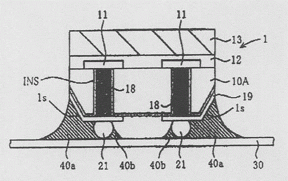
其次,如图6所示,通过沿切割线DL切割,分割半导体衬底10及其它各层,完成由半导体芯片10A及其它各层构成的半导体装置1。在此,在该半导体装置1的背面,形成从其半导体芯片10A的端部向侧面倾斜的倾斜面1s。Next, as shown in FIG. 6, the
其次,参照附图说明将上述的半导体装置1安装在电路衬底上的情况。图7是说明本发明实施例的半导体装置的剖面图。图7表示半导体装置1连接在例如印刷线路板等电路衬底30上时两者的剖面。另外,在电路衬底30上形成有未图示的导电图案。Next, a case where the above-mentioned semiconductor device 1 is mounted on a circuit board will be described with reference to the drawings. 7 is a cross-sectional view illustrating a semiconductor device according to an embodiment of the present invention. FIG. 7 shows a cross section of both when the semiconductor device 1 is connected to a
如图7所示,半导体装置1载置于电路衬底30上,使其背面(即形成有导电端子21侧的主面)与电路衬底80的表面(即形成有未图示的导电图案的一侧的主面)对向。As shown in FIG. 7 , the semiconductor device 1 is mounted on a
在此,在形成未图示的导电图案的电路衬底30的表面中,在和导电端子21相接的位置通过例如印刷法形成由例如焊锡或银(Ag)等构成的导电膏或导电性焊料(后述的回流处理之后表示为导电膏40a、40b)。Here, on the surface of the
为介由上述导电膏连接半导体装置1和电路衬底30,进行回流处理(即热处理)。通过该回流处理增加了流动性的导电膏40a、40b通过半导体装置1背面的倾斜面1s(即形成配线层19的倾斜面1s)的表面张力沿该倾斜面1s向半导体装置1的表面方向流动,同时,沿电路衬底30的水平方向向半导体装置1的外部流动。由此,不但导电端子21,连倾斜面1s也由导电膏40a、40b覆盖。因此,可最大限度地抑制现有例所见的导电端子和电路衬底的连接不良。另外,可提高半导体装置连接在电路衬底上时的机械强度。In order to connect the semiconductor device 1 and the
在正确地进行了上述连接时,从半导体装置1的表面来看,存在从半导体装置的侧面溢出的导电膏40a,即所谓的侧嵌条。因此,进行上述连接的半导体装置1的用户可通过观察该侧嵌条的有无,确认是否正确地进行了上述连接。When the above connection is correctly performed, the
另外,由于上倾斜面1s的表面张力,导电膏40a、40b具有沿电路衬底30朝向半导体装置1外部方向流动的倾向,故即使与现有例相比,在电路衬底30上形成大量的导电膏,也可以最大限度地抑制相邻的导电端子21间的空间被导电膏40b埋入。即,可最大限度地抑制导电端子21间短路。In addition, due to the surface tension of the upper
由于可提高半导体装置1连接在电路衬底30上时的机械强度,且最大限度地避免导电端子21间的短路,故可省略现有例所见的半导体装置的用户进行的底层填料91的形成工序。Since the mechanical strength when the semiconductor device 1 is connected to the
结果是可不使工序复杂而提高半导体装置安装时的强度及精度。As a result, the strength and precision at the time of semiconductor device mounting can be improved without complicating the process.
换句话说,在图7所示的半导体装置1中,在除半导体芯片10A的端部外的背面也可以覆盖该背面或配线层19形成未图示的保护层。在这种情况下,可进一步提高半导体装置的可靠性。In other words, in the semiconductor device 1 shown in FIG. 7 , a protective layer (not shown) may be formed on the back surface other than the end portion of the
另外,在上述的本实施例中,在半导体装置10A的背面形成有导电端子21,但本发明不限于此。即,本发明只要是形成贯通半导体芯片的埋入电极18及与其连接而延伸到倾斜面1s的配线层19的半导体装置,则也可以应用于未形成有导电端子21的半导体装置。此时,例如如图8所示,在半导体装置1L的半导体芯片10A的端部,覆盖埋入电极18上及倾斜面1s,在不存在导电端子的配线层19上形成含有和图7所示的相同的侧嵌条的导电膏40a、40b。In addition, in the present embodiment described above, the
Claims (12)
Applications Claiming Priority (2)
| Application Number | Priority Date | Filing Date | Title |
|---|---|---|---|
| JP2004152736 | 2004-05-24 | ||
| JP152736/04 | 2004-05-24 |
Publications (2)
| Publication Number | Publication Date |
|---|---|
| CN1702853A CN1702853A (en) | 2005-11-30 |
| CN100401503C true CN100401503C (en) | 2008-07-09 |
Family
ID=35446783
Family Applications (1)
| Application Number | Title | Priority Date | Filing Date |
|---|---|---|---|
| CNB2005100738045A Expired - Fee Related CN100401503C (en) | 2004-05-24 | 2005-05-24 | Semiconductor device and manufacturing method thereof |
Country Status (4)
| Country | Link |
|---|---|
| US (1) | US7504722B2 (en) |
| KR (1) | KR100673490B1 (en) |
| CN (1) | CN100401503C (en) |
| TW (1) | TWI272683B (en) |
Cited By (1)
| Publication number | Priority date | Publication date | Assignee | Title |
|---|---|---|---|---|
| CN111696948A (en) * | 2019-03-12 | 2020-09-22 | 爱思开海力士有限公司 | Semiconductor module including printed circuit board |
Families Citing this family (28)
| Publication number | Priority date | Publication date | Assignee | Title |
|---|---|---|---|---|
| US7179740B1 (en) * | 1999-05-03 | 2007-02-20 | United Microelectronics Corporation | Integrated circuit with improved interconnect structure and process for making same |
| JP2005235860A (en) * | 2004-02-17 | 2005-09-02 | Sanyo Electric Co Ltd | Semiconductor device and manufacturing method thereof |
| KR20080049807A (en) * | 2005-10-03 | 2008-06-04 | 로무 가부시키가이샤 | Semiconductor devices |
| DE102006003931B3 (en) * | 2006-01-26 | 2007-08-02 | Infineon Technologies Ag | Semiconductor device with external surface mount contacts and method of making the same |
| JP4812512B2 (en) * | 2006-05-19 | 2011-11-09 | オンセミコンダクター・トレーディング・リミテッド | Manufacturing method of semiconductor device |
| US7473577B2 (en) * | 2006-08-11 | 2009-01-06 | International Business Machines Corporation | Integrated chip carrier with compliant interconnect |
| US7749882B2 (en) * | 2006-08-23 | 2010-07-06 | Micron Technology, Inc. | Packaged microelectronic devices and methods for manufacturing packaged microelectronic devices |
| KR101382706B1 (en) * | 2007-01-30 | 2014-04-08 | 엘지이노텍 주식회사 | Stack-type semiconductor package |
| WO2008078899A1 (en) * | 2006-12-23 | 2008-07-03 | Lg Innotek Co., Ltd | Semiconductor package and manufacturing method thereof |
| US7666711B2 (en) * | 2008-05-27 | 2010-02-23 | Stats Chippac, Ltd. | Semiconductor device and method of forming double-sided through vias in saw streets |
| JP2010103300A (en) * | 2008-10-23 | 2010-05-06 | Sanyo Electric Co Ltd | Semiconductor device, and method of manufacturing the same |
| JP5395446B2 (en) * | 2009-01-22 | 2014-01-22 | ルネサスエレクトロニクス株式会社 | Semiconductor device and manufacturing method of semiconductor device |
| US10163766B2 (en) * | 2016-11-21 | 2018-12-25 | Semiconductor Components Industries, Llc | Methods of forming leadless semiconductor packages with plated leadframes and wettable flanks |
| US8283193B2 (en) * | 2009-08-14 | 2012-10-09 | Globalfoundries Singapore Pte. Ltd. | Integrated circuit system with sealring and method of manufacture thereof |
| US8093090B1 (en) * | 2009-10-12 | 2012-01-10 | Micron Technology, Inc. | Integrated circuit edge and method to fabricate the same |
| EP2405468A1 (en) * | 2010-07-05 | 2012-01-11 | ATOTECH Deutschland GmbH | Method to form solder deposits on substrates |
| KR101688006B1 (en) * | 2010-11-26 | 2016-12-20 | 삼성전자주식회사 | Semiconductor devices |
| DE102011080929B4 (en) * | 2011-08-12 | 2014-07-17 | Infineon Technologies Ag | Process for producing a composite and a power semiconductor module |
| US8552548B1 (en) | 2011-11-29 | 2013-10-08 | Amkor Technology, Inc. | Conductive pad on protruding through electrode semiconductor device |
| JP2016157880A (en) * | 2015-02-26 | 2016-09-01 | ルネサスエレクトロニクス株式会社 | Method of manufacturing semiconductor device, and semiconductor device |
| US10121742B2 (en) | 2017-03-15 | 2018-11-06 | Amkor Technology, Inc. | Method of forming a packaged semiconductor device using ganged conductive connective assembly and structure |
| US10290512B2 (en) | 2017-05-17 | 2019-05-14 | Nanya Technology Corporation | Semiconductor structure having bump on tilting upper corner surface |
| US10199312B1 (en) | 2017-09-09 | 2019-02-05 | Amkor Technology, Inc. | Method of forming a packaged semiconductor device having enhanced wettable flank and structure |
| US10366943B2 (en) | 2017-09-16 | 2019-07-30 | Amkor Technology, Inc. | Packaged electronic device having stepped conductive structure and related methods |
| KR102525161B1 (en) | 2018-07-16 | 2023-04-24 | 삼성전자주식회사 | Semiconductor device and semiconductor package comprising the same |
| CN217239442U (en) * | 2020-09-14 | 2022-08-19 | 意法半导体股份有限公司 | Packaged device and electronic device |
| IT202100014306A1 (en) * | 2021-06-01 | 2022-12-01 | St Microelectronics Srl | Process for manufacturing semiconductor devices and corresponding semiconductor device |
| US20230114872A1 (en) * | 2021-10-13 | 2023-04-13 | Texas Instruments Incorporated | Electronic device with wettable flank lead |
Citations (5)
| Publication number | Priority date | Publication date | Assignee | Title |
|---|---|---|---|---|
| CN1179009A (en) * | 1996-10-04 | 1998-04-15 | Lg半导体株式会社 | Semiconductor package and its socket |
| US5901046A (en) * | 1996-12-10 | 1999-05-04 | Denso Corporation | Surface mount type package unit and method for manufacturing the same |
| US6235554B1 (en) * | 1995-11-27 | 2001-05-22 | Micron Technology, Inc. | Method for fabricating stackable chip scale semiconductor package |
| US20010053567A1 (en) * | 1999-02-16 | 2001-12-20 | Salman Akram | Method of forming a test insert for interfacing a device containing contact bumps with a test substrate |
| US20020063332A1 (en) * | 2000-09-19 | 2002-05-30 | Yoshihide Yamaguchi | Semiconductor device and method for manufacturing the same and semiconductor device-mounted structure |
Family Cites Families (19)
| Publication number | Priority date | Publication date | Assignee | Title |
|---|---|---|---|---|
| US4862247A (en) * | 1987-11-24 | 1989-08-29 | Texas Instruments Incorporated | Contact joint for semiconductor chip carriers |
| US5973396A (en) * | 1996-02-16 | 1999-10-26 | Micron Technology, Inc. | Surface mount IC using silicon vias in an area array format or same size as die array |
| US6624505B2 (en) * | 1998-02-06 | 2003-09-23 | Shellcase, Ltd. | Packaged integrated circuits and methods of producing thereof |
| IL123207A0 (en) | 1998-02-06 | 1998-09-24 | Shellcase Ltd | Integrated circuit device |
| JP3497722B2 (en) | 1998-02-27 | 2004-02-16 | 富士通株式会社 | Semiconductor device, method of manufacturing the same, and transfer tray thereof |
| US5969461A (en) * | 1998-04-08 | 1999-10-19 | Cts Corporation | Surface acoustic wave device package and method |
| JP3677429B2 (en) | 2000-03-09 | 2005-08-03 | Necエレクトロニクス株式会社 | Method of manufacturing flip chip type semiconductor device |
| JP4020367B2 (en) * | 2001-04-17 | 2007-12-12 | 株式会社ルネサステクノロジ | Manufacturing method of semiconductor device |
| US6861757B2 (en) * | 2001-09-03 | 2005-03-01 | Nec Corporation | Interconnecting substrate for carrying semiconductor device, method of producing thereof and package of semiconductor device |
| US6552529B1 (en) * | 2001-12-17 | 2003-04-22 | International Business Machines Corporation | Method and apparatus for interim assembly electrical testing of circuit boards |
| JP2003229518A (en) | 2002-02-05 | 2003-08-15 | Sanyo Electric Co Ltd | Circuit device |
| JP4212293B2 (en) | 2002-04-15 | 2009-01-21 | 三洋電機株式会社 | Manufacturing method of semiconductor device |
| TWI232560B (en) * | 2002-04-23 | 2005-05-11 | Sanyo Electric Co | Semiconductor device and its manufacture |
| TWI227050B (en) * | 2002-10-11 | 2005-01-21 | Sanyo Electric Co | Semiconductor device and method for manufacturing the same |
| SG137651A1 (en) * | 2003-03-14 | 2007-12-28 | Micron Technology Inc | Microelectronic devices and methods for packaging microelectronic devices |
| JP4130158B2 (en) * | 2003-06-09 | 2008-08-06 | 三洋電機株式会社 | Semiconductor device manufacturing method, semiconductor device |
| JP4307284B2 (en) * | 2004-02-17 | 2009-08-05 | 三洋電機株式会社 | Manufacturing method of semiconductor device |
| US7129114B2 (en) * | 2004-03-10 | 2006-10-31 | Micron Technology, Inc. | Methods relating to singulating semiconductor wafers and wafer scale assemblies |
| JP4746847B2 (en) * | 2004-04-27 | 2011-08-10 | 三洋電機株式会社 | Manufacturing method of semiconductor device |
-
2005
- 2005-04-26 TW TW094113194A patent/TWI272683B/en not_active IP Right Cessation
- 2005-05-23 KR KR1020050042822A patent/KR100673490B1/en not_active Expired - Fee Related
- 2005-05-24 CN CNB2005100738045A patent/CN100401503C/en not_active Expired - Fee Related
- 2005-05-24 US US11/135,668 patent/US7504722B2/en not_active Expired - Lifetime
Patent Citations (5)
| Publication number | Priority date | Publication date | Assignee | Title |
|---|---|---|---|---|
| US6235554B1 (en) * | 1995-11-27 | 2001-05-22 | Micron Technology, Inc. | Method for fabricating stackable chip scale semiconductor package |
| CN1179009A (en) * | 1996-10-04 | 1998-04-15 | Lg半导体株式会社 | Semiconductor package and its socket |
| US5901046A (en) * | 1996-12-10 | 1999-05-04 | Denso Corporation | Surface mount type package unit and method for manufacturing the same |
| US20010053567A1 (en) * | 1999-02-16 | 2001-12-20 | Salman Akram | Method of forming a test insert for interfacing a device containing contact bumps with a test substrate |
| US20020063332A1 (en) * | 2000-09-19 | 2002-05-30 | Yoshihide Yamaguchi | Semiconductor device and method for manufacturing the same and semiconductor device-mounted structure |
Cited By (1)
| Publication number | Priority date | Publication date | Assignee | Title |
|---|---|---|---|---|
| CN111696948A (en) * | 2019-03-12 | 2020-09-22 | 爱思开海力士有限公司 | Semiconductor module including printed circuit board |
Also Published As
| Publication number | Publication date |
|---|---|
| KR100673490B1 (en) | 2007-01-24 |
| TW200608498A (en) | 2006-03-01 |
| US20050269696A1 (en) | 2005-12-08 |
| TWI272683B (en) | 2007-02-01 |
| CN1702853A (en) | 2005-11-30 |
| KR20060048058A (en) | 2006-05-18 |
| US7504722B2 (en) | 2009-03-17 |
Similar Documents
| Publication | Publication Date | Title |
|---|---|---|
| CN100401503C (en) | Semiconductor device and manufacturing method thereof | |
| KR100671921B1 (en) | Semiconductor device and manufacturing method thereof | |
| CN100383938C (en) | Semiconductor device and method for manufacturing the same | |
| KR100608184B1 (en) | Semiconductor device and method for manufacturing the same | |
| US8252630B2 (en) | Semiconductor device, method of manufacturing the semiconductor device, flip chip package having the semiconductor device and method of manufacturing the flip chip package | |
| JP4753170B2 (en) | Semiconductor device and manufacturing method thereof | |
| US20040136123A1 (en) | Circuit devices and method for manufacturing the same | |
| JP2005101268A (en) | Manufacturing method of semiconductor device | |
| JP2005019521A (en) | Manufacturing method of semiconductor device | |
| JP4828261B2 (en) | Semiconductor device and manufacturing method thereof | |
| JP4544902B2 (en) | Semiconductor device and manufacturing method thereof | |
| JP4282514B2 (en) | Manufacturing method of semiconductor device | |
| JP4518995B2 (en) | Semiconductor device and manufacturing method thereof | |
| JP2005311117A (en) | Semiconductor device and its manufacturing method | |
| KR100682004B1 (en) | Semiconductor devices | |
| US10930615B2 (en) | Semiconductor device and method of manufacturing semiconductor device | |
| JP4845986B2 (en) | Semiconductor device | |
| JP4769926B2 (en) | Semiconductor device and manufacturing method thereof | |
| JP2000236058A (en) | Semiconductor device and manufacturing method thereof | |
| JP2008041892A (en) | Semiconductor device and manufacturing method thereof | |
| JP2004327748A (en) | Semiconductor device and manufacturing method thereof |
Legal Events
| Date | Code | Title | Description |
|---|---|---|---|
| C06 | Publication | ||
| PB01 | Publication | ||
| C10 | Entry into substantive examination | ||
| SE01 | Entry into force of request for substantive examination | ||
| C14 | Grant of patent or utility model | ||
| GR01 | Patent grant | ||
| CF01 | Termination of patent right due to non-payment of annual fee | ||
| CF01 | Termination of patent right due to non-payment of annual fee |
Granted publication date: 20080709 Termination date: 20210524 |