CN100380661C - 分栅式功率模块以及用于抑制其中振荡的方法 - Google Patents
分栅式功率模块以及用于抑制其中振荡的方法 Download PDFInfo
- Publication number
- CN100380661C CN100380661C CNB03802909XA CN03802909A CN100380661C CN 100380661 C CN100380661 C CN 100380661C CN B03802909X A CNB03802909X A CN B03802909XA CN 03802909 A CN03802909 A CN 03802909A CN 100380661 C CN100380661 C CN 100380661C
- Authority
- CN
- China
- Prior art keywords
- grid
- tube core
- array
- area
- substrate
- Prior art date
- Legal status (The legal status is an assumption and is not a legal conclusion. Google has not performed a legal analysis and makes no representation as to the accuracy of the status listed.)
- Expired - Fee Related
Links
Images


Classifications
-
- H—ELECTRICITY
- H01—ELECTRIC ELEMENTS
- H01L—SEMICONDUCTOR DEVICES NOT COVERED BY CLASS H10
- H01L23/00—Details of semiconductor or other solid state devices
- H01L23/58—Structural electrical arrangements for semiconductor devices not otherwise provided for, e.g. in combination with batteries
- H01L23/64—Impedance arrangements
- H01L23/66—High-frequency adaptations
-
- H—ELECTRICITY
- H01—ELECTRIC ELEMENTS
- H01L—SEMICONDUCTOR DEVICES NOT COVERED BY CLASS H10
- H01L25/00—Assemblies consisting of a plurality of individual semiconductor or other solid state devices ; Multistep manufacturing processes thereof
- H01L25/03—Assemblies consisting of a plurality of individual semiconductor or other solid state devices ; Multistep manufacturing processes thereof all the devices being of a type provided for in the same subgroup of groups H01L27/00 - H01L33/00, or in a single subclass of H10K, H10N, e.g. assemblies of rectifier diodes
- H01L25/04—Assemblies consisting of a plurality of individual semiconductor or other solid state devices ; Multistep manufacturing processes thereof all the devices being of a type provided for in the same subgroup of groups H01L27/00 - H01L33/00, or in a single subclass of H10K, H10N, e.g. assemblies of rectifier diodes the devices not having separate containers
- H01L25/07—Assemblies consisting of a plurality of individual semiconductor or other solid state devices ; Multistep manufacturing processes thereof all the devices being of a type provided for in the same subgroup of groups H01L27/00 - H01L33/00, or in a single subclass of H10K, H10N, e.g. assemblies of rectifier diodes the devices not having separate containers the devices being of a type provided for in group H01L29/00
-
- H—ELECTRICITY
- H01—ELECTRIC ELEMENTS
- H01L—SEMICONDUCTOR DEVICES NOT COVERED BY CLASS H10
- H01L23/00—Details of semiconductor or other solid state devices
- H01L23/48—Arrangements for conducting electric current to or from the solid state body in operation, e.g. leads, terminal arrangements ; Selection of materials therefor
- H01L23/50—Arrangements for conducting electric current to or from the solid state body in operation, e.g. leads, terminal arrangements ; Selection of materials therefor for integrated circuit devices, e.g. power bus, number of leads
-
- H—ELECTRICITY
- H01—ELECTRIC ELEMENTS
- H01L—SEMICONDUCTOR DEVICES NOT COVERED BY CLASS H10
- H01L24/00—Arrangements for connecting or disconnecting semiconductor or solid-state bodies; Methods or apparatus related thereto
- H01L24/01—Means for bonding being attached to, or being formed on, the surface to be connected, e.g. chip-to-package, die-attach, "first-level" interconnects; Manufacturing methods related thereto
- H01L24/42—Wire connectors; Manufacturing methods related thereto
- H01L24/47—Structure, shape, material or disposition of the wire connectors after the connecting process
- H01L24/49—Structure, shape, material or disposition of the wire connectors after the connecting process of a plurality of wire connectors
-
- H—ELECTRICITY
- H01—ELECTRIC ELEMENTS
- H01L—SEMICONDUCTOR DEVICES NOT COVERED BY CLASS H10
- H01L25/00—Assemblies consisting of a plurality of individual semiconductor or other solid state devices ; Multistep manufacturing processes thereof
- H01L25/03—Assemblies consisting of a plurality of individual semiconductor or other solid state devices ; Multistep manufacturing processes thereof all the devices being of a type provided for in the same subgroup of groups H01L27/00 - H01L33/00, or in a single subclass of H10K, H10N, e.g. assemblies of rectifier diodes
- H01L25/04—Assemblies consisting of a plurality of individual semiconductor or other solid state devices ; Multistep manufacturing processes thereof all the devices being of a type provided for in the same subgroup of groups H01L27/00 - H01L33/00, or in a single subclass of H10K, H10N, e.g. assemblies of rectifier diodes the devices not having separate containers
- H01L25/07—Assemblies consisting of a plurality of individual semiconductor or other solid state devices ; Multistep manufacturing processes thereof all the devices being of a type provided for in the same subgroup of groups H01L27/00 - H01L33/00, or in a single subclass of H10K, H10N, e.g. assemblies of rectifier diodes the devices not having separate containers the devices being of a type provided for in group H01L29/00
- H01L25/072—Assemblies consisting of a plurality of individual semiconductor or other solid state devices ; Multistep manufacturing processes thereof all the devices being of a type provided for in the same subgroup of groups H01L27/00 - H01L33/00, or in a single subclass of H10K, H10N, e.g. assemblies of rectifier diodes the devices not having separate containers the devices being of a type provided for in group H01L29/00 the devices being arranged next to each other
-
- H—ELECTRICITY
- H01—ELECTRIC ELEMENTS
- H01L—SEMICONDUCTOR DEVICES NOT COVERED BY CLASS H10
- H01L2223/00—Details relating to semiconductor or other solid state devices covered by the group H01L23/00
- H01L2223/58—Structural electrical arrangements for semiconductor devices not otherwise provided for
- H01L2223/64—Impedance arrangements
- H01L2223/66—High-frequency adaptations
- H01L2223/6605—High-frequency electrical connections
- H01L2223/6627—Waveguides, e.g. microstrip line, strip line, coplanar line
-
- H—ELECTRICITY
- H01—ELECTRIC ELEMENTS
- H01L—SEMICONDUCTOR DEVICES NOT COVERED BY CLASS H10
- H01L2223/00—Details relating to semiconductor or other solid state devices covered by the group H01L23/00
- H01L2223/58—Structural electrical arrangements for semiconductor devices not otherwise provided for
- H01L2223/64—Impedance arrangements
- H01L2223/66—High-frequency adaptations
- H01L2223/6644—Packaging aspects of high-frequency amplifiers
-
- H—ELECTRICITY
- H01—ELECTRIC ELEMENTS
- H01L—SEMICONDUCTOR DEVICES NOT COVERED BY CLASS H10
- H01L2223/00—Details relating to semiconductor or other solid state devices covered by the group H01L23/00
- H01L2223/58—Structural electrical arrangements for semiconductor devices not otherwise provided for
- H01L2223/64—Impedance arrangements
- H01L2223/66—High-frequency adaptations
- H01L2223/6688—Mixed frequency adaptations, i.e. for operation at different frequencies
-
- H—ELECTRICITY
- H01—ELECTRIC ELEMENTS
- H01L—SEMICONDUCTOR DEVICES NOT COVERED BY CLASS H10
- H01L2224/00—Indexing scheme for arrangements for connecting or disconnecting semiconductor or solid-state bodies and methods related thereto as covered by H01L24/00
- H01L2224/01—Means for bonding being attached to, or being formed on, the surface to be connected, e.g. chip-to-package, die-attach, "first-level" interconnects; Manufacturing methods related thereto
- H01L2224/02—Bonding areas; Manufacturing methods related thereto
- H01L2224/04—Structure, shape, material or disposition of the bonding areas prior to the connecting process
- H01L2224/05—Structure, shape, material or disposition of the bonding areas prior to the connecting process of an individual bonding area
- H01L2224/0554—External layer
- H01L2224/05599—Material
- H01L2224/056—Material with a principal constituent of the material being a metal or a metalloid, e.g. boron [B], silicon [Si], germanium [Ge], arsenic [As], antimony [Sb], tellurium [Te] and polonium [Po], and alloys thereof
- H01L2224/05638—Material with a principal constituent of the material being a metal or a metalloid, e.g. boron [B], silicon [Si], germanium [Ge], arsenic [As], antimony [Sb], tellurium [Te] and polonium [Po], and alloys thereof the principal constituent melting at a temperature of greater than or equal to 950°C and less than 1550°C
- H01L2224/05639—Silver [Ag] as principal constituent
-
- H—ELECTRICITY
- H01—ELECTRIC ELEMENTS
- H01L—SEMICONDUCTOR DEVICES NOT COVERED BY CLASS H10
- H01L2224/00—Indexing scheme for arrangements for connecting or disconnecting semiconductor or solid-state bodies and methods related thereto as covered by H01L24/00
- H01L2224/01—Means for bonding being attached to, or being formed on, the surface to be connected, e.g. chip-to-package, die-attach, "first-level" interconnects; Manufacturing methods related thereto
- H01L2224/42—Wire connectors; Manufacturing methods related thereto
- H01L2224/44—Structure, shape, material or disposition of the wire connectors prior to the connecting process
- H01L2224/45—Structure, shape, material or disposition of the wire connectors prior to the connecting process of an individual wire connector
- H01L2224/45001—Core members of the connector
- H01L2224/45099—Material
- H01L2224/451—Material with a principal constituent of the material being a metal or a metalloid, e.g. boron (B), silicon (Si), germanium (Ge), arsenic (As), antimony (Sb), tellurium (Te) and polonium (Po), and alloys thereof
- H01L2224/45117—Material with a principal constituent of the material being a metal or a metalloid, e.g. boron (B), silicon (Si), germanium (Ge), arsenic (As), antimony (Sb), tellurium (Te) and polonium (Po), and alloys thereof the principal constituent melting at a temperature of greater than or equal to 400°C and less than 950°C
- H01L2224/45124—Aluminium (Al) as principal constituent
-
- H—ELECTRICITY
- H01—ELECTRIC ELEMENTS
- H01L—SEMICONDUCTOR DEVICES NOT COVERED BY CLASS H10
- H01L2224/00—Indexing scheme for arrangements for connecting or disconnecting semiconductor or solid-state bodies and methods related thereto as covered by H01L24/00
- H01L2224/01—Means for bonding being attached to, or being formed on, the surface to be connected, e.g. chip-to-package, die-attach, "first-level" interconnects; Manufacturing methods related thereto
- H01L2224/42—Wire connectors; Manufacturing methods related thereto
- H01L2224/44—Structure, shape, material or disposition of the wire connectors prior to the connecting process
- H01L2224/45—Structure, shape, material or disposition of the wire connectors prior to the connecting process of an individual wire connector
- H01L2224/45001—Core members of the connector
- H01L2224/45099—Material
- H01L2224/451—Material with a principal constituent of the material being a metal or a metalloid, e.g. boron (B), silicon (Si), germanium (Ge), arsenic (As), antimony (Sb), tellurium (Te) and polonium (Po), and alloys thereof
- H01L2224/45138—Material with a principal constituent of the material being a metal or a metalloid, e.g. boron (B), silicon (Si), germanium (Ge), arsenic (As), antimony (Sb), tellurium (Te) and polonium (Po), and alloys thereof the principal constituent melting at a temperature of greater than or equal to 950°C and less than 1550°C
- H01L2224/45139—Silver (Ag) as principal constituent
-
- H—ELECTRICITY
- H01—ELECTRIC ELEMENTS
- H01L—SEMICONDUCTOR DEVICES NOT COVERED BY CLASS H10
- H01L2224/00—Indexing scheme for arrangements for connecting or disconnecting semiconductor or solid-state bodies and methods related thereto as covered by H01L24/00
- H01L2224/01—Means for bonding being attached to, or being formed on, the surface to be connected, e.g. chip-to-package, die-attach, "first-level" interconnects; Manufacturing methods related thereto
- H01L2224/42—Wire connectors; Manufacturing methods related thereto
- H01L2224/44—Structure, shape, material or disposition of the wire connectors prior to the connecting process
- H01L2224/45—Structure, shape, material or disposition of the wire connectors prior to the connecting process of an individual wire connector
- H01L2224/45001—Core members of the connector
- H01L2224/45099—Material
- H01L2224/451—Material with a principal constituent of the material being a metal or a metalloid, e.g. boron (B), silicon (Si), germanium (Ge), arsenic (As), antimony (Sb), tellurium (Te) and polonium (Po), and alloys thereof
- H01L2224/45138—Material with a principal constituent of the material being a metal or a metalloid, e.g. boron (B), silicon (Si), germanium (Ge), arsenic (As), antimony (Sb), tellurium (Te) and polonium (Po), and alloys thereof the principal constituent melting at a temperature of greater than or equal to 950°C and less than 1550°C
- H01L2224/45144—Gold (Au) as principal constituent
-
- H—ELECTRICITY
- H01—ELECTRIC ELEMENTS
- H01L—SEMICONDUCTOR DEVICES NOT COVERED BY CLASS H10
- H01L2224/00—Indexing scheme for arrangements for connecting or disconnecting semiconductor or solid-state bodies and methods related thereto as covered by H01L24/00
- H01L2224/01—Means for bonding being attached to, or being formed on, the surface to be connected, e.g. chip-to-package, die-attach, "first-level" interconnects; Manufacturing methods related thereto
- H01L2224/42—Wire connectors; Manufacturing methods related thereto
- H01L2224/47—Structure, shape, material or disposition of the wire connectors after the connecting process
- H01L2224/48—Structure, shape, material or disposition of the wire connectors after the connecting process of an individual wire connector
- H01L2224/4805—Shape
- H01L2224/4809—Loop shape
- H01L2224/48091—Arched
-
- H—ELECTRICITY
- H01—ELECTRIC ELEMENTS
- H01L—SEMICONDUCTOR DEVICES NOT COVERED BY CLASS H10
- H01L2224/00—Indexing scheme for arrangements for connecting or disconnecting semiconductor or solid-state bodies and methods related thereto as covered by H01L24/00
- H01L2224/01—Means for bonding being attached to, or being formed on, the surface to be connected, e.g. chip-to-package, die-attach, "first-level" interconnects; Manufacturing methods related thereto
- H01L2224/42—Wire connectors; Manufacturing methods related thereto
- H01L2224/47—Structure, shape, material or disposition of the wire connectors after the connecting process
- H01L2224/48—Structure, shape, material or disposition of the wire connectors after the connecting process of an individual wire connector
- H01L2224/485—Material
- H01L2224/48505—Material at the bonding interface
- H01L2224/48599—Principal constituent of the connecting portion of the wire connector being Gold (Au)
- H01L2224/486—Principal constituent of the connecting portion of the wire connector being Gold (Au) with a principal constituent of the bonding area being a metal or a metalloid, e.g. boron (B), silicon (Si), germanium (Ge), arsenic (As), antimony (Sb), tellurium (Te) and polonium (Po), and alloys thereof
- H01L2224/48638—Principal constituent of the connecting portion of the wire connector being Gold (Au) with a principal constituent of the bonding area being a metal or a metalloid, e.g. boron (B), silicon (Si), germanium (Ge), arsenic (As), antimony (Sb), tellurium (Te) and polonium (Po), and alloys thereof the principal constituent melting at a temperature of greater than or equal to 950°C and less than 1550°C
- H01L2224/48639—Silver (Ag) as principal constituent
-
- H—ELECTRICITY
- H01—ELECTRIC ELEMENTS
- H01L—SEMICONDUCTOR DEVICES NOT COVERED BY CLASS H10
- H01L2224/00—Indexing scheme for arrangements for connecting or disconnecting semiconductor or solid-state bodies and methods related thereto as covered by H01L24/00
- H01L2224/01—Means for bonding being attached to, or being formed on, the surface to be connected, e.g. chip-to-package, die-attach, "first-level" interconnects; Manufacturing methods related thereto
- H01L2224/42—Wire connectors; Manufacturing methods related thereto
- H01L2224/47—Structure, shape, material or disposition of the wire connectors after the connecting process
- H01L2224/48—Structure, shape, material or disposition of the wire connectors after the connecting process of an individual wire connector
- H01L2224/485—Material
- H01L2224/48505—Material at the bonding interface
- H01L2224/48699—Principal constituent of the connecting portion of the wire connector being Aluminium (Al)
- H01L2224/487—Principal constituent of the connecting portion of the wire connector being Aluminium (Al) with a principal constituent of the bonding area being a metal or a metalloid, e.g. boron (B), silicon (Si), germanium (Ge), arsenic (As), antimony (Sb), tellurium (Te) and polonium (Po), and alloys thereof
- H01L2224/48738—Principal constituent of the connecting portion of the wire connector being Aluminium (Al) with a principal constituent of the bonding area being a metal or a metalloid, e.g. boron (B), silicon (Si), germanium (Ge), arsenic (As), antimony (Sb), tellurium (Te) and polonium (Po), and alloys thereof the principal constituent melting at a temperature of greater than or equal to 950°C and less than 1550°C
- H01L2224/48739—Silver (Ag) as principal constituent
-
- H—ELECTRICITY
- H01—ELECTRIC ELEMENTS
- H01L—SEMICONDUCTOR DEVICES NOT COVERED BY CLASS H10
- H01L2224/00—Indexing scheme for arrangements for connecting or disconnecting semiconductor or solid-state bodies and methods related thereto as covered by H01L24/00
- H01L2224/01—Means for bonding being attached to, or being formed on, the surface to be connected, e.g. chip-to-package, die-attach, "first-level" interconnects; Manufacturing methods related thereto
- H01L2224/42—Wire connectors; Manufacturing methods related thereto
- H01L2224/47—Structure, shape, material or disposition of the wire connectors after the connecting process
- H01L2224/49—Structure, shape, material or disposition of the wire connectors after the connecting process of a plurality of wire connectors
- H01L2224/491—Disposition
- H01L2224/4912—Layout
- H01L2224/49171—Fan-out arrangements
-
- H—ELECTRICITY
- H01—ELECTRIC ELEMENTS
- H01L—SEMICONDUCTOR DEVICES NOT COVERED BY CLASS H10
- H01L2224/00—Indexing scheme for arrangements for connecting or disconnecting semiconductor or solid-state bodies and methods related thereto as covered by H01L24/00
- H01L2224/01—Means for bonding being attached to, or being formed on, the surface to be connected, e.g. chip-to-package, die-attach, "first-level" interconnects; Manufacturing methods related thereto
- H01L2224/42—Wire connectors; Manufacturing methods related thereto
- H01L2224/47—Structure, shape, material or disposition of the wire connectors after the connecting process
- H01L2224/49—Structure, shape, material or disposition of the wire connectors after the connecting process of a plurality of wire connectors
- H01L2224/491—Disposition
- H01L2224/4912—Layout
- H01L2224/49175—Parallel arrangements
-
- H—ELECTRICITY
- H01—ELECTRIC ELEMENTS
- H01L—SEMICONDUCTOR DEVICES NOT COVERED BY CLASS H10
- H01L23/00—Details of semiconductor or other solid state devices
- H01L23/58—Structural electrical arrangements for semiconductor devices not otherwise provided for, e.g. in combination with batteries
- H01L23/64—Impedance arrangements
- H01L23/645—Inductive arrangements
-
- H—ELECTRICITY
- H01—ELECTRIC ELEMENTS
- H01L—SEMICONDUCTOR DEVICES NOT COVERED BY CLASS H10
- H01L24/00—Arrangements for connecting or disconnecting semiconductor or solid-state bodies; Methods or apparatus related thereto
- H01L24/01—Means for bonding being attached to, or being formed on, the surface to be connected, e.g. chip-to-package, die-attach, "first-level" interconnects; Manufacturing methods related thereto
- H01L24/42—Wire connectors; Manufacturing methods related thereto
- H01L24/44—Structure, shape, material or disposition of the wire connectors prior to the connecting process
- H01L24/45—Structure, shape, material or disposition of the wire connectors prior to the connecting process of an individual wire connector
-
- H—ELECTRICITY
- H01—ELECTRIC ELEMENTS
- H01L—SEMICONDUCTOR DEVICES NOT COVERED BY CLASS H10
- H01L24/00—Arrangements for connecting or disconnecting semiconductor or solid-state bodies; Methods or apparatus related thereto
- H01L24/01—Means for bonding being attached to, or being formed on, the surface to be connected, e.g. chip-to-package, die-attach, "first-level" interconnects; Manufacturing methods related thereto
- H01L24/42—Wire connectors; Manufacturing methods related thereto
- H01L24/47—Structure, shape, material or disposition of the wire connectors after the connecting process
- H01L24/48—Structure, shape, material or disposition of the wire connectors after the connecting process of an individual wire connector
-
- H—ELECTRICITY
- H01—ELECTRIC ELEMENTS
- H01L—SEMICONDUCTOR DEVICES NOT COVERED BY CLASS H10
- H01L2924/00—Indexing scheme for arrangements or methods for connecting or disconnecting semiconductor or solid-state bodies as covered by H01L24/00
- H01L2924/0001—Technical content checked by a classifier
- H01L2924/00011—Not relevant to the scope of the group, the symbol of which is combined with the symbol of this group
-
- H—ELECTRICITY
- H01—ELECTRIC ELEMENTS
- H01L—SEMICONDUCTOR DEVICES NOT COVERED BY CLASS H10
- H01L2924/00—Indexing scheme for arrangements or methods for connecting or disconnecting semiconductor or solid-state bodies as covered by H01L24/00
- H01L2924/0001—Technical content checked by a classifier
- H01L2924/00014—Technical content checked by a classifier the subject-matter covered by the group, the symbol of which is combined with the symbol of this group, being disclosed without further technical details
-
- H—ELECTRICITY
- H01—ELECTRIC ELEMENTS
- H01L—SEMICONDUCTOR DEVICES NOT COVERED BY CLASS H10
- H01L2924/00—Indexing scheme for arrangements or methods for connecting or disconnecting semiconductor or solid-state bodies as covered by H01L24/00
- H01L2924/01—Chemical elements
- H01L2924/01013—Aluminum [Al]
-
- H—ELECTRICITY
- H01—ELECTRIC ELEMENTS
- H01L—SEMICONDUCTOR DEVICES NOT COVERED BY CLASS H10
- H01L2924/00—Indexing scheme for arrangements or methods for connecting or disconnecting semiconductor or solid-state bodies as covered by H01L24/00
- H01L2924/01—Chemical elements
- H01L2924/01047—Silver [Ag]
-
- H—ELECTRICITY
- H01—ELECTRIC ELEMENTS
- H01L—SEMICONDUCTOR DEVICES NOT COVERED BY CLASS H10
- H01L2924/00—Indexing scheme for arrangements or methods for connecting or disconnecting semiconductor or solid-state bodies as covered by H01L24/00
- H01L2924/01—Chemical elements
- H01L2924/01058—Cerium [Ce]
-
- H—ELECTRICITY
- H01—ELECTRIC ELEMENTS
- H01L—SEMICONDUCTOR DEVICES NOT COVERED BY CLASS H10
- H01L2924/00—Indexing scheme for arrangements or methods for connecting or disconnecting semiconductor or solid-state bodies as covered by H01L24/00
- H01L2924/01—Chemical elements
- H01L2924/01079—Gold [Au]
-
- H—ELECTRICITY
- H01—ELECTRIC ELEMENTS
- H01L—SEMICONDUCTOR DEVICES NOT COVERED BY CLASS H10
- H01L2924/00—Indexing scheme for arrangements or methods for connecting or disconnecting semiconductor or solid-state bodies as covered by H01L24/00
- H01L2924/10—Details of semiconductor or other solid state devices to be connected
- H01L2924/11—Device type
- H01L2924/13—Discrete devices, e.g. 3 terminal devices
- H01L2924/1304—Transistor
- H01L2924/1306—Field-effect transistor [FET]
- H01L2924/13063—Metal-Semiconductor Field-Effect Transistor [MESFET]
-
- H—ELECTRICITY
- H01—ELECTRIC ELEMENTS
- H01L—SEMICONDUCTOR DEVICES NOT COVERED BY CLASS H10
- H01L2924/00—Indexing scheme for arrangements or methods for connecting or disconnecting semiconductor or solid-state bodies as covered by H01L24/00
- H01L2924/10—Details of semiconductor or other solid state devices to be connected
- H01L2924/11—Device type
- H01L2924/13—Discrete devices, e.g. 3 terminal devices
- H01L2924/1304—Transistor
- H01L2924/1306—Field-effect transistor [FET]
- H01L2924/13091—Metal-Oxide-Semiconductor Field-Effect Transistor [MOSFET]
-
- H—ELECTRICITY
- H01—ELECTRIC ELEMENTS
- H01L—SEMICONDUCTOR DEVICES NOT COVERED BY CLASS H10
- H01L2924/00—Indexing scheme for arrangements or methods for connecting or disconnecting semiconductor or solid-state bodies as covered by H01L24/00
- H01L2924/15—Details of package parts other than the semiconductor or other solid state devices to be connected
- H01L2924/151—Die mounting substrate
- H01L2924/156—Material
- H01L2924/15786—Material with a principal constituent of the material being a non metallic, non metalloid inorganic material
- H01L2924/15787—Ceramics, e.g. crystalline carbides, nitrides or oxides
-
- H—ELECTRICITY
- H01—ELECTRIC ELEMENTS
- H01L—SEMICONDUCTOR DEVICES NOT COVERED BY CLASS H10
- H01L2924/00—Indexing scheme for arrangements or methods for connecting or disconnecting semiconductor or solid-state bodies as covered by H01L24/00
- H01L2924/19—Details of hybrid assemblies other than the semiconductor or other solid state devices to be connected
- H01L2924/1901—Structure
- H01L2924/1903—Structure including wave guides
- H01L2924/19032—Structure including wave guides being a microstrip line type
-
- H—ELECTRICITY
- H01—ELECTRIC ELEMENTS
- H01L—SEMICONDUCTOR DEVICES NOT COVERED BY CLASS H10
- H01L2924/00—Indexing scheme for arrangements or methods for connecting or disconnecting semiconductor or solid-state bodies as covered by H01L24/00
- H01L2924/19—Details of hybrid assemblies other than the semiconductor or other solid state devices to be connected
- H01L2924/1901—Structure
- H01L2924/1904—Component type
- H01L2924/19042—Component type being an inductor
-
- H—ELECTRICITY
- H01—ELECTRIC ELEMENTS
- H01L—SEMICONDUCTOR DEVICES NOT COVERED BY CLASS H10
- H01L2924/00—Indexing scheme for arrangements or methods for connecting or disconnecting semiconductor or solid-state bodies as covered by H01L24/00
- H01L2924/19—Details of hybrid assemblies other than the semiconductor or other solid state devices to be connected
- H01L2924/1901—Structure
- H01L2924/1904—Component type
- H01L2924/19043—Component type being a resistor
-
- H—ELECTRICITY
- H01—ELECTRIC ELEMENTS
- H01L—SEMICONDUCTOR DEVICES NOT COVERED BY CLASS H10
- H01L2924/00—Indexing scheme for arrangements or methods for connecting or disconnecting semiconductor or solid-state bodies as covered by H01L24/00
- H01L2924/30—Technical effects
- H01L2924/301—Electrical effects
- H01L2924/30105—Capacitance
-
- H—ELECTRICITY
- H01—ELECTRIC ELEMENTS
- H01L—SEMICONDUCTOR DEVICES NOT COVERED BY CLASS H10
- H01L2924/00—Indexing scheme for arrangements or methods for connecting or disconnecting semiconductor or solid-state bodies as covered by H01L24/00
- H01L2924/30—Technical effects
- H01L2924/301—Electrical effects
- H01L2924/30107—Inductance
-
- H—ELECTRICITY
- H01—ELECTRIC ELEMENTS
- H01L—SEMICONDUCTOR DEVICES NOT COVERED BY CLASS H10
- H01L2924/00—Indexing scheme for arrangements or methods for connecting or disconnecting semiconductor or solid-state bodies as covered by H01L24/00
- H01L2924/30—Technical effects
- H01L2924/301—Electrical effects
- H01L2924/3011—Impedance
- H01L2924/30111—Impedance matching
Abstract
本发明涉及一种将四个功率晶体管管芯封装并互相连接的方法,使每个功率晶体管管芯工作在第一频率,在高于所述第一频率但低于相应晶体管管芯的截止频率的第二频率不发生振荡。本方法包括将所述管芯固定到基片上,使每个管芯的漏极与所述基片上的导电层的第一区域电气地和热学地结合;电气地将每个管芯的源极与所述基片上所述导电层的第二区域连接;且通过相应的电导线,电气地将每个管芯的栅极与所述基片上所述导电层的第三公用的内部中心区域连接。所述电导线被制成实质上相同的电长度,并提供相应于所述电长度的第一阻抗以无衰减地传递所述第一频率;提供从一个管芯栅极到另一个管芯栅极的第二阻抗以衰减所述第二频率。
Description
技术领域
本发明涉及包含多个晶体管而只提供一个单一外接栅极端口的功率模块。更具体而言,它涉及一个功率模块,工作在第一频率,而在低于该晶体管的截止频率之下的第二更高频率不发生振荡。
背景技术
利用多个晶体管管芯的现有技术功率模块装置已被大家所知。图1和图2所示为两个这样现有技术的结构,图1所示为一个已知为SGS托普生TH430的装置,图2所示为一个已知为东芝TPM1919的装置。
图1所示的SGS托普生TH430是一个四个管芯的双极性器件,取用一个中央基极接点与位于矩形阵列外侧的发射极相连。在本设计中未作使从基极端口到各个管芯基极的路径长度相等的安排。可认为管芯的上限频率,这里指晶体管的截止频率,与该四管芯器件的50MHz的上限频率接近。
图2所示的东芝TPM1919是一个具有四个直线排列MESFET管芯的2GHz的器件。该装置利用一个“梯状”分割结构将栅极信号分成四路。在栅极连接与分割结构的末端之间存在匹配网络。可认为这些匹配网络在预期的工作频率下提供阻抗变换,以帮助实现该器件。该器件的输入结构提供一定的平衡与隔离功能,其工作频率据信是在接近于各个管芯的上限频率。
因此,已知的现有技术器件工作在管芯的频率范围的顶端。由于涉及到非常高的频率,现有技术的栅极以及/或者基极导线必需是短的。因此,它们的寄生谐振(以及潜在的振荡)频率高于管芯增益用尽时的频率。因此存在很少的振荡,或者没有振荡。
美国专利号4639760描述的Motorola设计MRF154(FIG.2’)使用串联栅极电阻,有意地大幅度减少各个栅极元件的增益以充分防止振荡。管芯具有大于500MHz的增益响应,但是整个器件的预期频率范围小于100MHz。因此Motorola设计具有过剩增益。
发明内容
本发明涉及一种将四个功率晶体管管芯封装并互相连接的方法,每个晶体管管芯工作在第一频率,在高于第一频率但低于晶体管管芯截止频率的第二频率下不发生振荡。本方法包括将多个管芯固定到一个基片上,将每个管芯的低侧面(漏极)与所述基片上的导电层的第一区域电气地和热学地结合;电气地将每个管芯的源极与所述基片上的所述导电层的第二区域连接;以及通过相应的电导线,电气地连接每个管芯的栅极到所述基片上所述导电层的第三公用的内部中心区域。
所述电导线被制成大致相同的电长度,并提供相应于从公共区域到各个栅极的所述电长度的第一阻抗,将基本无衰减地传递第一频率;并且提供了从一个管芯的栅极到另一个管芯的栅极的第二阻抗,它将大幅度衰减第二个频率。根据第一实施例,该导线采取具有一个或者多个跳线与薄膜电阻串联的形式。根据第二实施例,其采取的形式为具有一个或者多个具有预定阻抗特征的曲折带状线,并具有一个或者多个栅极焊接片,通过长跳线与其各自对应的栅极相连接。
附图简要说明
图1所示为现有技术的功率放大器。
图2所示为另一个现有技术的功率放大器
图2’所示为第三个现有技术的功率放大器
图3为本发明第一实施例的示意图。
图4为本发明第二实施例的示意图。
图5为图3所示实施例中的栅极结构的一个更为详细的示意图。
图6为图4所示实施例中的栅极结构的一个更为详细的示意图。
详细描述
根据本发明,四个功率MOSFET晶体管管芯以矩形阵列,例如正方形阵列排列,如图3和图4所示。这些管芯具有250MHz的上限值,但它们的尺寸大小是Motorola设计中管芯的两倍。因此,根据本发明,这些晶体管的输入电容高。该高电容降低了晶体管寄生结构的谐振频率,当晶体管并联在一个功率模块中时,这能够导致振荡。由于高的输入电容以及源极电阻的使用,如根据本发明的第一实施例,在预期工作频率下的增益起初就不是很高。因此,存在很少的过剩增益,而且仅栅极电阻就减少了总放大增益。如果抑制振荡所需的电阻太高,则可以使用电感器代替。因此本发明第二实施例利用栅极电感器代替栅极电阻,并提供较高的无振荡增益。
本发明可看作是为RF功率应用而设计的,提供一种可靠、易行且可重复制造、含多个功率MOSFET管芯的模块化结构。
图3所示为本发明具有均衡栅极输入连接的第一实施例,其中连接利用的是印刷串联电阻。本领域的专业人员能领会,在第一实施例中,所得到的是一个比较低增益的放大器,但确是一个可运作而无不良振荡的放大器。专业人员也会理解,为了增加该放大器实例的增益,可以使用具有较大增益的较小管芯,从而串联电阻在预期工作频率下不会消耗大部分的增益余量。
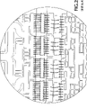
图3所示为四管芯(各标注为1)阵列固定在一个最好是陶瓷(例如BeO)的基片2上,该基片提供一个导电的源极连接区域3,一个导电的漏极连接区域4,以及一个导电的栅极连接区域5。薄膜源极电阻6(例如钯金)位于管芯阵列周界外侧的基片上。如图所示,提供了栅极连接导线7和源极连接导线8(例如铝),以及源极连接片9(例如银)。跳线10(例如铝)从栅极连接区域5延伸到一个居中的栅极接线(landing)区L处,L与栅极串联电阻13相邻,并与其电气连接。栅极电阻13的远端通过栅极连接导线7线接到每个管芯1上的多个对应的栅极接线区上。
图4所示为本发明具有均衡栅极输入连接的第二实施例,该连接利用的是具有比较高本征电感的印刷曲折带状线或者带状连接线11。由于电感带状线的感抗依赖于频率(和不依赖于频率的电阻的阻抗不同),因此在发明的这种第二实施例中有可能获得较高的增益而无振荡。从而可以理解,第二实施例的设计布局与第一种相似:其中栅极的第一个管芯外连接将位于一个公用的内部居中区域内。专业人员也会认识到,虽然很低,但带状线本质上也具有特性电阻和电容。
从图4可以看出曲折带状线具有大体相等的电长度,例如,它们表现出几乎相同的阻抗(包括电阻,电感和电容),并且从外部栅极端5’通过跳线10延伸到一个居中的公用接线区L’处,其中L’位于管芯阵列的内部及相邻管芯之间。曲折状电感器终止于栅极连接片12’处,在此通过栅极连接导线7’线接到每个管芯1上的多个对应的栅极连接片上。可以理解到基片2,源极连接区域3,漏极连接区域4,源极电阻6,源极连接导线8,以及源极连接片9,与图3所示的上述本发明第一实施例中的那些大体相同。本领域的专业人员可以理解,带状线的曲折特性有效地延长了导线的电气长度,而无须大幅度增大所需的连接布线面积。
图5为一个仅显示图3所示装置的栅极连接区域的详细示意图。图5突出了上述的用于该器件的栅极连接5和连接导线7。它也显示了第二个(居中的)栅极连接导线10(根据所示的第一实施例有六条),在栅极连接5与居中的栅极接线区L之间提供了一个可控阻抗(例如电阻的/电感的/电容的)路径。它进一步显示了栅极连接片12(每个管芯各一个)。最后,图5显示了优选印刷电路电阻13(也是每个管芯各一个)。对于一个给定的应用,跳线10的数量及其长度可以调整以获得所需的电感、电阻和载流量。
根据优选的第一实施例,栅极串联电阻约为3欧姆或更小。本领域的专业人员会理解,串联电阻的阻值是选用来在器件的一个给定的工作频率下有效地抑制振荡,同时不减少多于必需的器件的总体增益。而且,正如优选第一实施例所示,六根细跳线10是平行排列的。
图6为一个仅显示图4所示装置的栅极连接区域的详细示意图。参考图4如上所述,第二实施例省略了栅极串联电阻13,将栅极连接片12’改组为占用一个更小的尺度,并加入四个可控阻抗带状线连接线11,如图所示延伸在一个公用居中接线区L’与连接片12’之间。如图3和图5所示,接线区L’可看出是通过六根平行跳线10与栅极连接5’相连接。
可控阻抗带状线的典型特性阻抗--与所选的管芯兼容--约为90欧姆,是由其宽度、厚度以及基片2的介电特性所决定的。根据上述图4和图6所示的本发明第二实施例,带状线大约为0.65英寸长,0.013英寸宽,而基片约为40密耳厚。管芯1本身的输入阻抗大约低于0.2欧姆。
本领域的专业人员会理解,导体宽度与介质层厚度的比值决定特性阻抗,导体长度决定曲折带状线加注在栅极和公用连接点L’之间的串联阻抗。本领域的专业人员也会理解,在本发明的思想和范围之内,所示的带状线可以用不同方法来定性,制造以及/或者布线。
基于说明的目的,描述了一个四管芯的矩形阵列。其他几何形状排列,圆形、三角形等,具有更多或更少管芯,也可以由上述方法来应用,而且是在本发明的思想和范围之内。
因此,在一个优选实施例中已经说明、描述了我们的发明原理,对于本领域的专业人员来说应该是非常明显,可以在不背离这些原理的情况下对本发明的安排和细节作修改。我们对所有的在下述权利要求的思想和范围之内的更改均要求权利。
Claims (16)
1.一种将多个功率晶体管管芯封装并互相连接的方法,每个功率晶体管管芯工作于第一频率,并在高于所述第一频率但低于相应的晶体管管芯的截止频率的第二频率不发生振荡,该方法包括:
将所述管芯固定到基片上,使每个管芯的漏极与所述基片上的导电层的第一区域电气地和热学地结合;
电气地将每个管芯的源极与所述基片上所述导电层的第二区域连接;以及
通过相应的电导线,电气地将每个管芯的栅极与所述基片上所述导电层的第三公用的内部中心接线区域连接,
所述电导线被制成实质上相同的电长度,并提供相应于从所述第三公用的内部中心接线区域到各个栅极的所述电长度的第一阻抗,所述第一阻抗将无衰减地传递所述第一频率;并且提供从一个管芯栅极到另一个管芯栅极的第二阻抗,所述第二阻抗将衰减所述第二频率。
2.根据权利要求1所述的方法,其中所述多个管芯被排列成一个阵列,并且所述基片配置成使与所述源极相连接的所述第二区域位于阵列以外,且所述第三公用的内部中心接线区域位于阵列的内部且居中并在所述管芯之间。
3.根据权利要求1所述的方法,其中所述多个管芯排列为一阵列,并进一步包括连接所述第三公用的内部中心接线区域和连接至外部栅极端的第四区域的一组导电的第一跳线,其中所述基片配置成使与所述源极相连接的所述第二区域位于阵列以外在所述基片的相对的第一侧面和第二侧面,所述第三公用的内部中心接线区域位于阵列内居中的位置,且所述第四区域在阵列之外。
4.根据权利要求1所述的方法,其中每个电导线各包括第一部分、第二部分和第三部分,所述第一部分从所述第三公用的内部中心接线区域延伸到对应于各自管芯的栅极的栅极连接片区域,所述第一部分包括一个或多个可控阻抗薄膜,所述第二部分与所述第一部分串联连接,所述第二部分包括所述栅极连接片区域,所述第三部分与所述第二部分串联连接,所述第三部分包括一个或多个延伸到所述各自管芯的所述栅极的导电跳线。
5.根据权利要求4所述的方法,其中至少每个电导线的第一部分和第二部分是在所述导电层内一体形成的,以在所述基片上勾画出相等的、定义的阻抗的线,具有相等的电阻、电感和电容;并且其中所述导电跳线被配置成具有相等的、定义的阻抗,以将每个栅极连接片区域连接到各自的栅极。
6.根据权利要求1所述的方法,其中所述电导线各自包括第一部分,所述第一部分在所述导电层内一体形成,并且在所述第三公用的内部中心接线区域和与对应于所述管芯之一的电气分离的栅极连接片区域之间延伸,所述第一部分具有曲折带状线的形状,且其中所述电导线各包括第二部分,所述第二部分包括第一组多个导电跳线,所述第一组多个导电跳线配置成具有相等的、定义的阻抗,以将每个栅极连接片区域连接到各自的栅极。
7.根据权利要求6所述的方法,其中所述多个管芯排列为一阵列,进一步包括连接第三公用的内部中心接线区域和连接至外部栅极端的第四区域的一组导电的第一跳线,且其中所述基片配置成使连接至所述源极的所述第二区域位于所述阵列以外在所述基片的相对的第一侧面和第二侧面上,所述第三公用的内部中心接线区域位于所述阵列中居中的位置,并且所述第四区域在所述阵列之外。
8.根据权利要求2、3或7所述的方法,其中的阵列是矩形。
9.一种将多个功率晶体管管芯封装并互相连接的功率模块,每个功率晶体管管芯工作于第一频率,并在高于所述第一频率但低于相应的晶体管管芯的截止频率的第二频率不发生振荡,所述模块包括:
具有导电层的基片,所述导电层划分形成第一区域、第二区域和第三公用的内部中心连线区域;
固定到所述基片上的多个功率晶体管管芯,每个管芯的漏极与所述基片上所述导电层的所述第一区域电气地和热学地结合;
每个管芯的源极与所述基片上的所述导电层的所述第二区域电气地连接;以及
每个管芯的栅极通过相应的电导线电气地连接到所述基片上的所述导电层的所述第三公用的内部中心接线区域,
所述电导线被制成实质上相同的电长度,并提供相应于从所述第三公用的内部中心接线区域到各个栅极的所述电长度的第一阻抗,所述第一阻抗将无衰减地传递所述第一频率;并且提供从一个管芯栅极到另一个管芯栅极的第二阻抗,所述第二阻抗将衰减所述第二频率。
10.根据权利要求9所述的功率模块,其中所述多个管芯被排列成一个阵列,并且所述基片配置成使与所述源极连接的所述第二区域位于所述阵列以外,且第三公用的内部中心接线区域位于所述阵列的内部居中位置并在管芯之间。
11.根据权利要求9所述的功率模块,其中所述多个管芯排列为一阵列,进一步包括连接第三公用的内部中心接线区域和连接至外部栅极端的第四区域的一组导电的第一跳线,且其中所述基片配置成使与所述源极连接的所述第二区域位于所述阵列以外在所述基片的相对的第一侧面和第二侧面上,所述第三公用的内部中心接线区域位于所述阵列内居中的位置,且所述第四区域在所述阵列之外。
12.根据权利要求9所述的功率模块,其中每个电导线各包括第一部分、第二部分和第三部分,所述第一部分从所述第三公用的内部中心接线区域延伸到对应于各自管芯栅极的栅极连接片区域,所述第一部分包括一个或多个可控阻抗薄膜,所述第二部分与所述第一部分串联连接,所述第二部分包括所述栅极连接片区域,所述第三部分与所述第二部分串联连接,所述第三部分包括一个或多个延伸到各自管芯栅极的导电跳线。
13.根据权利要求12所述的功率模块,其中至少每个电导线的第一部分和第二部分是在所述导电层内一体形成的,以在所述基片上勾画出相等的、定义的阻抗的线,具有相等的电阻、电感和电容;并且其中导电跳线被配置成具有相等的、定义的阻抗,以将每个栅极连接片区域连接到各自的栅极。
14.根据权利要求9所述的功率模块,其中所述电导线各自包括第一部分,所述第一部分在导电层内一体形成的,并且在所述第三公用的内部中心接线区域和与对应于所述管芯之一的电气分离的栅极连接片区域之间延伸,所述第一部分具有曲折带状线的形状,且其中所述导线各包括第二部分,所述第二部分包括第一组多个导电跳线,所述第一组多个导电跳线配置成具有相等的、定义的阻抗,以将每个栅极连接片区域连接到各自的栅极。
15.根据权利要求14所述的功率模块,其中所述多个管芯排列为一阵列,进一步包括连接第三公用的内部中心接线区域和连接至外部栅极端的第四区域的一组导电的第一跳线,且其中所述基片配置成使连接至所述源极的所述第二区域位于阵列以外在所述基片的相对的第一侧面和第二侧面上,所述第三公用的内部中心接线区域位于所述阵列中居中的位置,并且所述第四区域在所述阵列之外。
16.根据权利要求10、11或15所述的功率模块,其中的阵列是矩形。
Applications Claiming Priority (2)
| Application Number | Priority Date | Filing Date | Title |
|---|---|---|---|
| US35380902P | 2002-01-29 | 2002-01-29 | |
| US60/353,809 | 2002-01-29 |
Publications (2)
| Publication Number | Publication Date |
|---|---|
| CN1625807A CN1625807A (zh) | 2005-06-08 |
| CN100380661C true CN100380661C (zh) | 2008-04-09 |
Family
ID=27663256
Family Applications (1)
| Application Number | Title | Priority Date | Filing Date |
|---|---|---|---|
| CNB03802909XA Expired - Fee Related CN100380661C (zh) | 2002-01-29 | 2003-01-27 | 分栅式功率模块以及用于抑制其中振荡的方法 |
Country Status (8)
| Country | Link |
|---|---|
| US (2) | US6939743B2 (zh) |
| EP (1) | EP1470588B1 (zh) |
| JP (1) | JP4732692B2 (zh) |
| KR (1) | KR20040085169A (zh) |
| CN (1) | CN100380661C (zh) |
| AT (1) | ATE339013T1 (zh) |
| DE (1) | DE60308148T2 (zh) |
| WO (1) | WO2003065454A2 (zh) |
Families Citing this family (11)
| Publication number | Priority date | Publication date | Assignee | Title |
|---|---|---|---|---|
| JP4342232B2 (ja) * | 2003-07-11 | 2009-10-14 | 三菱電機株式会社 | 半導体パワーモジュールおよび該モジュールの主回路電流値を計測する主回路電流計測システム |
| GB201105912D0 (en) * | 2011-04-07 | 2011-05-18 | Diamond Microwave Devices Ltd | Improved matching techniques for power transistors |
| US8581660B1 (en) * | 2012-04-24 | 2013-11-12 | Texas Instruments Incorporated | Power transistor partial current sensing for high precision applications |
| EP2862202B1 (en) * | 2012-06-19 | 2016-04-27 | ABB Technology AG | Substrate for mounting multiple power transistors thereon and power semiconductor module |
| DE102014111931B4 (de) * | 2014-08-20 | 2021-07-08 | Infineon Technologies Ag | Niederinduktive Schaltungsanordnung mit Laststromsammelleiterbahn |
| CN110050339B (zh) * | 2016-12-16 | 2023-12-22 | 日立能源有限公司 | 具有低栅极通路电感的功率半导体模块 |
| JP6838243B2 (ja) | 2017-09-29 | 2021-03-03 | 日立Astemo株式会社 | 電力変換装置 |
| DE102019112935B4 (de) | 2019-05-16 | 2021-04-29 | Danfoss Silicon Power Gmbh | Halbleitermodul |
| JP6772355B1 (ja) * | 2019-10-15 | 2020-10-21 | 株式会社京三製作所 | スイッチングモジュール |
| JP7351209B2 (ja) | 2019-12-17 | 2023-09-27 | 富士電機株式会社 | 半導体装置 |
| JP2021097146A (ja) | 2019-12-18 | 2021-06-24 | 富士電機株式会社 | 半導体装置 |
Citations (3)
| Publication number | Priority date | Publication date | Assignee | Title |
|---|---|---|---|---|
| US4907068A (en) * | 1987-01-21 | 1990-03-06 | Siemens Aktiengesellschaft | Semiconductor arrangement having at least one semiconductor body |
| US5563447A (en) * | 1993-09-07 | 1996-10-08 | Delco Electronics Corp. | High power semiconductor switch module |
| US5731970A (en) * | 1989-12-22 | 1998-03-24 | Hitachi, Ltd. | Power conversion device and semiconductor module suitable for use in the device |
Family Cites Families (13)
| Publication number | Priority date | Publication date | Assignee | Title |
|---|---|---|---|---|
| US4639760A (en) | 1986-01-21 | 1987-01-27 | Motorola, Inc. | High power RF transistor assembly |
| JP2751707B2 (ja) * | 1992-01-29 | 1998-05-18 | 株式会社日立製作所 | 半導体モジュール及びそれを使った電力変換装置 |
| JPH04183001A (ja) * | 1990-11-16 | 1992-06-30 | Mitsubishi Electric Corp | マイクロ波ic用パッケージ |
| JPH0575314A (ja) * | 1991-09-13 | 1993-03-26 | Matsushita Electron Corp | マイクロ波集積回路素子 |
| JP3053298B2 (ja) * | 1992-08-19 | 2000-06-19 | 株式会社東芝 | 半導体装置 |
| DE59304797D1 (de) * | 1992-08-26 | 1997-01-30 | Eupec Gmbh & Co Kg | Leistungshalbleiter-Modul |
| US6291878B1 (en) * | 1993-04-22 | 2001-09-18 | Sundstrand Corporation | Package for multiple high power electrical components |
| JP2973799B2 (ja) * | 1993-04-23 | 1999-11-08 | 富士電機株式会社 | パワートランジスタモジュール |
| DE19644009A1 (de) * | 1996-10-31 | 1998-05-07 | Siemens Ag | Großflächiges Hochstrommodul eines feldgesteuerten, abschaltbaren Leistungs-Halbleiterschalters |
| JP2000323647A (ja) * | 1999-05-12 | 2000-11-24 | Toshiba Corp | モジュール型半導体装置及びその製造方法 |
| JP4163818B2 (ja) * | 1999-07-07 | 2008-10-08 | 三菱電機株式会社 | 内部整合型トランジスタ |
| JP4138192B2 (ja) * | 1999-12-27 | 2008-08-20 | 三菱電機株式会社 | 半導体スイッチ装置 |
| US6617679B2 (en) * | 2002-02-08 | 2003-09-09 | Advanced Energy Industries, Inc. | Semiconductor package for multiple high power transistors |
-
2003
- 2003-01-27 JP JP2003564937A patent/JP4732692B2/ja not_active Expired - Lifetime
- 2003-01-27 DE DE60308148T patent/DE60308148T2/de not_active Expired - Fee Related
- 2003-01-27 US US10/352,314 patent/US6939743B2/en not_active Expired - Lifetime
- 2003-01-27 CN CNB03802909XA patent/CN100380661C/zh not_active Expired - Fee Related
- 2003-01-27 EP EP03705914A patent/EP1470588B1/en not_active Expired - Lifetime
- 2003-01-27 AT AT03705914T patent/ATE339013T1/de not_active IP Right Cessation
- 2003-01-27 WO PCT/US2003/002326 patent/WO2003065454A2/en active IP Right Grant
- 2003-01-27 KR KR10-2004-7011632A patent/KR20040085169A/ko not_active Application Discontinuation
-
2005
- 2005-06-03 US US11/145,042 patent/US7342262B2/en not_active Expired - Lifetime
Patent Citations (3)
| Publication number | Priority date | Publication date | Assignee | Title |
|---|---|---|---|---|
| US4907068A (en) * | 1987-01-21 | 1990-03-06 | Siemens Aktiengesellschaft | Semiconductor arrangement having at least one semiconductor body |
| US5731970A (en) * | 1989-12-22 | 1998-03-24 | Hitachi, Ltd. | Power conversion device and semiconductor module suitable for use in the device |
| US5563447A (en) * | 1993-09-07 | 1996-10-08 | Delco Electronics Corp. | High power semiconductor switch module |
Also Published As
| Publication number | Publication date |
|---|---|
| WO2003065454A3 (en) | 2004-02-26 |
| CN1625807A (zh) | 2005-06-08 |
| DE60308148T2 (de) | 2007-08-16 |
| JP4732692B2 (ja) | 2011-07-27 |
| US20050218500A1 (en) | 2005-10-06 |
| EP1470588B1 (en) | 2006-09-06 |
| US6939743B2 (en) | 2005-09-06 |
| US7342262B2 (en) | 2008-03-11 |
| EP1470588A2 (en) | 2004-10-27 |
| DE60308148D1 (de) | 2006-10-19 |
| ATE339013T1 (de) | 2006-09-15 |
| JP2006502560A (ja) | 2006-01-19 |
| US20030141587A1 (en) | 2003-07-31 |
| WO2003065454A2 (en) | 2003-08-07 |
| KR20040085169A (ko) | 2004-10-07 |
Similar Documents
| Publication | Publication Date | Title |
|---|---|---|
| CN103681635B (zh) | 具有阻抗匹配电路的半导体装置及其制造方法 | |
| US7342262B2 (en) | Split-gate power module for suppressing oscillation therein | |
| US8295057B2 (en) | Semiconductor device | |
| CN106409783B (zh) | 具有集成电气功能的基于pcb的半导体封装 | |
| US20160344353A1 (en) | Rf amplifier output circuit device with integrated current path, and methods of manufacture thereof | |
| US9820401B2 (en) | Packaged RF power transistor device having next to each other a ground and a video lead for connecting a decoupling capacitor, RF power amplifier | |
| CN106470019A (zh) | 射频放大器模块以及制造射频放大器模块的方法 | |
| CN107070419A (zh) | 用于rf放大器器件的输出阻抗匹配电路及其制造方法 | |
| CN102184917A (zh) | 采用四方扁平无引脚封装的gsm射频发射前端模块 | |
| JPS59229842A (ja) | ブツシユプル半導体デバイス用のパツケ−ジ | |
| EP2722880B1 (en) | Packaged RF amplifier circuit | |
| CN105762117A (zh) | 一种ltcc基板的交错层叠三维封装结构 | |
| CN107026625A (zh) | 具有集成混合耦合器的rf器件封装 | |
| TW449958B (en) | Semiconductor device | |
| CN101847627B (zh) | 集成无源器件的半导体芯片及功率放大器器件 | |
| JP2006502560A5 (zh) | ||
| US10784822B2 (en) | High power radio frequency amplifiers and methods of manufacture thereof | |
| CN215600357U (zh) | 一种高功率密度的sop8l封装引线框架 | |
| EP2509105A1 (en) | Semiconductor device having improved performance for high RF output powers | |
| US10784821B2 (en) | High power radio frequency amplifiers and methods of manufacture thereof | |
| CN100375279C (zh) | 一种集成电路中的去耦网络 | |
| US20200195205A1 (en) | RF Amplifier with Impedance Matching Components Monolithically Integrated in Transistor Die | |
| CN218827106U (zh) | 异构封装基板和异构封装模组 | |
| JP2870503B2 (ja) | ヘテロ接合バイポーラトランジスタ | |
| JPS647682B2 (zh) |
Legal Events
| Date | Code | Title | Description |
|---|---|---|---|
| C06 | Publication | ||
| PB01 | Publication | ||
| C10 | Entry into substantive examination | ||
| SE01 | Entry into force of request for substantive examination | ||
| C14 | Grant of patent or utility model | ||
| GR01 | Patent grant | ||
| C17 | Cessation of patent right | ||
| CF01 | Termination of patent right due to non-payment of annual fee |
Granted publication date: 20080409 Termination date: 20100301 |