EP1470588B1 - Split-gate power module and method for suppressing oscillation therein - Google Patents
Split-gate power module and method for suppressing oscillation therein Download PDFInfo
- Publication number
- EP1470588B1 EP1470588B1 EP03705914A EP03705914A EP1470588B1 EP 1470588 B1 EP1470588 B1 EP 1470588B1 EP 03705914 A EP03705914 A EP 03705914A EP 03705914 A EP03705914 A EP 03705914A EP 1470588 B1 EP1470588 B1 EP 1470588B1
- Authority
- EP
- European Patent Office
- Prior art keywords
- area
- gate
- array
- substrate
- die
- Prior art date
- Legal status (The legal status is an assumption and is not a legal conclusion. Google has not performed a legal analysis and makes no representation as to the accuracy of the status listed.)
- Expired - Lifetime
Links
Images

Classifications
-
- H—ELECTRICITY
- H01—ELECTRIC ELEMENTS
- H01L—SEMICONDUCTOR DEVICES NOT COVERED BY CLASS H10
- H01L23/00—Details of semiconductor or other solid state devices
- H01L23/58—Structural electrical arrangements for semiconductor devices not otherwise provided for, e.g. in combination with batteries
- H01L23/64—Impedance arrangements
- H01L23/66—High-frequency adaptations
-
- H—ELECTRICITY
- H01—ELECTRIC ELEMENTS
- H01L—SEMICONDUCTOR DEVICES NOT COVERED BY CLASS H10
- H01L25/00—Assemblies consisting of a plurality of individual semiconductor or other solid state devices ; Multistep manufacturing processes thereof
- H01L25/03—Assemblies consisting of a plurality of individual semiconductor or other solid state devices ; Multistep manufacturing processes thereof all the devices being of a type provided for in the same subgroup of groups H01L27/00 - H01L33/00, or in a single subclass of H10K, H10N, e.g. assemblies of rectifier diodes
- H01L25/04—Assemblies consisting of a plurality of individual semiconductor or other solid state devices ; Multistep manufacturing processes thereof all the devices being of a type provided for in the same subgroup of groups H01L27/00 - H01L33/00, or in a single subclass of H10K, H10N, e.g. assemblies of rectifier diodes the devices not having separate containers
- H01L25/07—Assemblies consisting of a plurality of individual semiconductor or other solid state devices ; Multistep manufacturing processes thereof all the devices being of a type provided for in the same subgroup of groups H01L27/00 - H01L33/00, or in a single subclass of H10K, H10N, e.g. assemblies of rectifier diodes the devices not having separate containers the devices being of a type provided for in group H01L29/00
-
- H—ELECTRICITY
- H01—ELECTRIC ELEMENTS
- H01L—SEMICONDUCTOR DEVICES NOT COVERED BY CLASS H10
- H01L23/00—Details of semiconductor or other solid state devices
- H01L23/48—Arrangements for conducting electric current to or from the solid state body in operation, e.g. leads, terminal arrangements ; Selection of materials therefor
- H01L23/50—Arrangements for conducting electric current to or from the solid state body in operation, e.g. leads, terminal arrangements ; Selection of materials therefor for integrated circuit devices, e.g. power bus, number of leads
-
- H—ELECTRICITY
- H01—ELECTRIC ELEMENTS
- H01L—SEMICONDUCTOR DEVICES NOT COVERED BY CLASS H10
- H01L24/00—Arrangements for connecting or disconnecting semiconductor or solid-state bodies; Methods or apparatus related thereto
- H01L24/01—Means for bonding being attached to, or being formed on, the surface to be connected, e.g. chip-to-package, die-attach, "first-level" interconnects; Manufacturing methods related thereto
- H01L24/42—Wire connectors; Manufacturing methods related thereto
- H01L24/47—Structure, shape, material or disposition of the wire connectors after the connecting process
- H01L24/49—Structure, shape, material or disposition of the wire connectors after the connecting process of a plurality of wire connectors
-
- H—ELECTRICITY
- H01—ELECTRIC ELEMENTS
- H01L—SEMICONDUCTOR DEVICES NOT COVERED BY CLASS H10
- H01L25/00—Assemblies consisting of a plurality of individual semiconductor or other solid state devices ; Multistep manufacturing processes thereof
- H01L25/03—Assemblies consisting of a plurality of individual semiconductor or other solid state devices ; Multistep manufacturing processes thereof all the devices being of a type provided for in the same subgroup of groups H01L27/00 - H01L33/00, or in a single subclass of H10K, H10N, e.g. assemblies of rectifier diodes
- H01L25/04—Assemblies consisting of a plurality of individual semiconductor or other solid state devices ; Multistep manufacturing processes thereof all the devices being of a type provided for in the same subgroup of groups H01L27/00 - H01L33/00, or in a single subclass of H10K, H10N, e.g. assemblies of rectifier diodes the devices not having separate containers
- H01L25/07—Assemblies consisting of a plurality of individual semiconductor or other solid state devices ; Multistep manufacturing processes thereof all the devices being of a type provided for in the same subgroup of groups H01L27/00 - H01L33/00, or in a single subclass of H10K, H10N, e.g. assemblies of rectifier diodes the devices not having separate containers the devices being of a type provided for in group H01L29/00
- H01L25/072—Assemblies consisting of a plurality of individual semiconductor or other solid state devices ; Multistep manufacturing processes thereof all the devices being of a type provided for in the same subgroup of groups H01L27/00 - H01L33/00, or in a single subclass of H10K, H10N, e.g. assemblies of rectifier diodes the devices not having separate containers the devices being of a type provided for in group H01L29/00 the devices being arranged next to each other
-
- H—ELECTRICITY
- H01—ELECTRIC ELEMENTS
- H01L—SEMICONDUCTOR DEVICES NOT COVERED BY CLASS H10
- H01L2223/00—Details relating to semiconductor or other solid state devices covered by the group H01L23/00
- H01L2223/58—Structural electrical arrangements for semiconductor devices not otherwise provided for
- H01L2223/64—Impedance arrangements
- H01L2223/66—High-frequency adaptations
- H01L2223/6605—High-frequency electrical connections
- H01L2223/6627—Waveguides, e.g. microstrip line, strip line, coplanar line
-
- H—ELECTRICITY
- H01—ELECTRIC ELEMENTS
- H01L—SEMICONDUCTOR DEVICES NOT COVERED BY CLASS H10
- H01L2223/00—Details relating to semiconductor or other solid state devices covered by the group H01L23/00
- H01L2223/58—Structural electrical arrangements for semiconductor devices not otherwise provided for
- H01L2223/64—Impedance arrangements
- H01L2223/66—High-frequency adaptations
- H01L2223/6644—Packaging aspects of high-frequency amplifiers
-
- H—ELECTRICITY
- H01—ELECTRIC ELEMENTS
- H01L—SEMICONDUCTOR DEVICES NOT COVERED BY CLASS H10
- H01L2223/00—Details relating to semiconductor or other solid state devices covered by the group H01L23/00
- H01L2223/58—Structural electrical arrangements for semiconductor devices not otherwise provided for
- H01L2223/64—Impedance arrangements
- H01L2223/66—High-frequency adaptations
- H01L2223/6688—Mixed frequency adaptations, i.e. for operation at different frequencies
-
- H—ELECTRICITY
- H01—ELECTRIC ELEMENTS
- H01L—SEMICONDUCTOR DEVICES NOT COVERED BY CLASS H10
- H01L2224/00—Indexing scheme for arrangements for connecting or disconnecting semiconductor or solid-state bodies and methods related thereto as covered by H01L24/00
- H01L2224/01—Means for bonding being attached to, or being formed on, the surface to be connected, e.g. chip-to-package, die-attach, "first-level" interconnects; Manufacturing methods related thereto
- H01L2224/02—Bonding areas; Manufacturing methods related thereto
- H01L2224/04—Structure, shape, material or disposition of the bonding areas prior to the connecting process
- H01L2224/05—Structure, shape, material or disposition of the bonding areas prior to the connecting process of an individual bonding area
- H01L2224/0554—External layer
- H01L2224/05599—Material
- H01L2224/056—Material with a principal constituent of the material being a metal or a metalloid, e.g. boron [B], silicon [Si], germanium [Ge], arsenic [As], antimony [Sb], tellurium [Te] and polonium [Po], and alloys thereof
- H01L2224/05638—Material with a principal constituent of the material being a metal or a metalloid, e.g. boron [B], silicon [Si], germanium [Ge], arsenic [As], antimony [Sb], tellurium [Te] and polonium [Po], and alloys thereof the principal constituent melting at a temperature of greater than or equal to 950°C and less than 1550°C
- H01L2224/05639—Silver [Ag] as principal constituent
-
- H—ELECTRICITY
- H01—ELECTRIC ELEMENTS
- H01L—SEMICONDUCTOR DEVICES NOT COVERED BY CLASS H10
- H01L2224/00—Indexing scheme for arrangements for connecting or disconnecting semiconductor or solid-state bodies and methods related thereto as covered by H01L24/00
- H01L2224/01—Means for bonding being attached to, or being formed on, the surface to be connected, e.g. chip-to-package, die-attach, "first-level" interconnects; Manufacturing methods related thereto
- H01L2224/42—Wire connectors; Manufacturing methods related thereto
- H01L2224/44—Structure, shape, material or disposition of the wire connectors prior to the connecting process
- H01L2224/45—Structure, shape, material or disposition of the wire connectors prior to the connecting process of an individual wire connector
- H01L2224/45001—Core members of the connector
- H01L2224/45099—Material
- H01L2224/451—Material with a principal constituent of the material being a metal or a metalloid, e.g. boron (B), silicon (Si), germanium (Ge), arsenic (As), antimony (Sb), tellurium (Te) and polonium (Po), and alloys thereof
- H01L2224/45117—Material with a principal constituent of the material being a metal or a metalloid, e.g. boron (B), silicon (Si), germanium (Ge), arsenic (As), antimony (Sb), tellurium (Te) and polonium (Po), and alloys thereof the principal constituent melting at a temperature of greater than or equal to 400°C and less than 950°C
- H01L2224/45124—Aluminium (Al) as principal constituent
-
- H—ELECTRICITY
- H01—ELECTRIC ELEMENTS
- H01L—SEMICONDUCTOR DEVICES NOT COVERED BY CLASS H10
- H01L2224/00—Indexing scheme for arrangements for connecting or disconnecting semiconductor or solid-state bodies and methods related thereto as covered by H01L24/00
- H01L2224/01—Means for bonding being attached to, or being formed on, the surface to be connected, e.g. chip-to-package, die-attach, "first-level" interconnects; Manufacturing methods related thereto
- H01L2224/42—Wire connectors; Manufacturing methods related thereto
- H01L2224/44—Structure, shape, material or disposition of the wire connectors prior to the connecting process
- H01L2224/45—Structure, shape, material or disposition of the wire connectors prior to the connecting process of an individual wire connector
- H01L2224/45001—Core members of the connector
- H01L2224/45099—Material
- H01L2224/451—Material with a principal constituent of the material being a metal or a metalloid, e.g. boron (B), silicon (Si), germanium (Ge), arsenic (As), antimony (Sb), tellurium (Te) and polonium (Po), and alloys thereof
- H01L2224/45138—Material with a principal constituent of the material being a metal or a metalloid, e.g. boron (B), silicon (Si), germanium (Ge), arsenic (As), antimony (Sb), tellurium (Te) and polonium (Po), and alloys thereof the principal constituent melting at a temperature of greater than or equal to 950°C and less than 1550°C
- H01L2224/45139—Silver (Ag) as principal constituent
-
- H—ELECTRICITY
- H01—ELECTRIC ELEMENTS
- H01L—SEMICONDUCTOR DEVICES NOT COVERED BY CLASS H10
- H01L2224/00—Indexing scheme for arrangements for connecting or disconnecting semiconductor or solid-state bodies and methods related thereto as covered by H01L24/00
- H01L2224/01—Means for bonding being attached to, or being formed on, the surface to be connected, e.g. chip-to-package, die-attach, "first-level" interconnects; Manufacturing methods related thereto
- H01L2224/42—Wire connectors; Manufacturing methods related thereto
- H01L2224/44—Structure, shape, material or disposition of the wire connectors prior to the connecting process
- H01L2224/45—Structure, shape, material or disposition of the wire connectors prior to the connecting process of an individual wire connector
- H01L2224/45001—Core members of the connector
- H01L2224/45099—Material
- H01L2224/451—Material with a principal constituent of the material being a metal or a metalloid, e.g. boron (B), silicon (Si), germanium (Ge), arsenic (As), antimony (Sb), tellurium (Te) and polonium (Po), and alloys thereof
- H01L2224/45138—Material with a principal constituent of the material being a metal or a metalloid, e.g. boron (B), silicon (Si), germanium (Ge), arsenic (As), antimony (Sb), tellurium (Te) and polonium (Po), and alloys thereof the principal constituent melting at a temperature of greater than or equal to 950°C and less than 1550°C
- H01L2224/45144—Gold (Au) as principal constituent
-
- H—ELECTRICITY
- H01—ELECTRIC ELEMENTS
- H01L—SEMICONDUCTOR DEVICES NOT COVERED BY CLASS H10
- H01L2224/00—Indexing scheme for arrangements for connecting or disconnecting semiconductor or solid-state bodies and methods related thereto as covered by H01L24/00
- H01L2224/01—Means for bonding being attached to, or being formed on, the surface to be connected, e.g. chip-to-package, die-attach, "first-level" interconnects; Manufacturing methods related thereto
- H01L2224/42—Wire connectors; Manufacturing methods related thereto
- H01L2224/47—Structure, shape, material or disposition of the wire connectors after the connecting process
- H01L2224/48—Structure, shape, material or disposition of the wire connectors after the connecting process of an individual wire connector
- H01L2224/4805—Shape
- H01L2224/4809—Loop shape
- H01L2224/48091—Arched
-
- H—ELECTRICITY
- H01—ELECTRIC ELEMENTS
- H01L—SEMICONDUCTOR DEVICES NOT COVERED BY CLASS H10
- H01L2224/00—Indexing scheme for arrangements for connecting or disconnecting semiconductor or solid-state bodies and methods related thereto as covered by H01L24/00
- H01L2224/01—Means for bonding being attached to, or being formed on, the surface to be connected, e.g. chip-to-package, die-attach, "first-level" interconnects; Manufacturing methods related thereto
- H01L2224/42—Wire connectors; Manufacturing methods related thereto
- H01L2224/47—Structure, shape, material or disposition of the wire connectors after the connecting process
- H01L2224/48—Structure, shape, material or disposition of the wire connectors after the connecting process of an individual wire connector
- H01L2224/485—Material
- H01L2224/48505—Material at the bonding interface
- H01L2224/48599—Principal constituent of the connecting portion of the wire connector being Gold (Au)
- H01L2224/486—Principal constituent of the connecting portion of the wire connector being Gold (Au) with a principal constituent of the bonding area being a metal or a metalloid, e.g. boron (B), silicon (Si), germanium (Ge), arsenic (As), antimony (Sb), tellurium (Te) and polonium (Po), and alloys thereof
- H01L2224/48638—Principal constituent of the connecting portion of the wire connector being Gold (Au) with a principal constituent of the bonding area being a metal or a metalloid, e.g. boron (B), silicon (Si), germanium (Ge), arsenic (As), antimony (Sb), tellurium (Te) and polonium (Po), and alloys thereof the principal constituent melting at a temperature of greater than or equal to 950°C and less than 1550°C
- H01L2224/48639—Silver (Ag) as principal constituent
-
- H—ELECTRICITY
- H01—ELECTRIC ELEMENTS
- H01L—SEMICONDUCTOR DEVICES NOT COVERED BY CLASS H10
- H01L2224/00—Indexing scheme for arrangements for connecting or disconnecting semiconductor or solid-state bodies and methods related thereto as covered by H01L24/00
- H01L2224/01—Means for bonding being attached to, or being formed on, the surface to be connected, e.g. chip-to-package, die-attach, "first-level" interconnects; Manufacturing methods related thereto
- H01L2224/42—Wire connectors; Manufacturing methods related thereto
- H01L2224/47—Structure, shape, material or disposition of the wire connectors after the connecting process
- H01L2224/48—Structure, shape, material or disposition of the wire connectors after the connecting process of an individual wire connector
- H01L2224/485—Material
- H01L2224/48505—Material at the bonding interface
- H01L2224/48699—Principal constituent of the connecting portion of the wire connector being Aluminium (Al)
- H01L2224/487—Principal constituent of the connecting portion of the wire connector being Aluminium (Al) with a principal constituent of the bonding area being a metal or a metalloid, e.g. boron (B), silicon (Si), germanium (Ge), arsenic (As), antimony (Sb), tellurium (Te) and polonium (Po), and alloys thereof
- H01L2224/48738—Principal constituent of the connecting portion of the wire connector being Aluminium (Al) with a principal constituent of the bonding area being a metal or a metalloid, e.g. boron (B), silicon (Si), germanium (Ge), arsenic (As), antimony (Sb), tellurium (Te) and polonium (Po), and alloys thereof the principal constituent melting at a temperature of greater than or equal to 950°C and less than 1550°C
- H01L2224/48739—Silver (Ag) as principal constituent
-
- H—ELECTRICITY
- H01—ELECTRIC ELEMENTS
- H01L—SEMICONDUCTOR DEVICES NOT COVERED BY CLASS H10
- H01L2224/00—Indexing scheme for arrangements for connecting or disconnecting semiconductor or solid-state bodies and methods related thereto as covered by H01L24/00
- H01L2224/01—Means for bonding being attached to, or being formed on, the surface to be connected, e.g. chip-to-package, die-attach, "first-level" interconnects; Manufacturing methods related thereto
- H01L2224/42—Wire connectors; Manufacturing methods related thereto
- H01L2224/47—Structure, shape, material or disposition of the wire connectors after the connecting process
- H01L2224/49—Structure, shape, material or disposition of the wire connectors after the connecting process of a plurality of wire connectors
- H01L2224/491—Disposition
- H01L2224/4912—Layout
- H01L2224/49171—Fan-out arrangements
-
- H—ELECTRICITY
- H01—ELECTRIC ELEMENTS
- H01L—SEMICONDUCTOR DEVICES NOT COVERED BY CLASS H10
- H01L2224/00—Indexing scheme for arrangements for connecting or disconnecting semiconductor or solid-state bodies and methods related thereto as covered by H01L24/00
- H01L2224/01—Means for bonding being attached to, or being formed on, the surface to be connected, e.g. chip-to-package, die-attach, "first-level" interconnects; Manufacturing methods related thereto
- H01L2224/42—Wire connectors; Manufacturing methods related thereto
- H01L2224/47—Structure, shape, material or disposition of the wire connectors after the connecting process
- H01L2224/49—Structure, shape, material or disposition of the wire connectors after the connecting process of a plurality of wire connectors
- H01L2224/491—Disposition
- H01L2224/4912—Layout
- H01L2224/49175—Parallel arrangements
-
- H—ELECTRICITY
- H01—ELECTRIC ELEMENTS
- H01L—SEMICONDUCTOR DEVICES NOT COVERED BY CLASS H10
- H01L23/00—Details of semiconductor or other solid state devices
- H01L23/58—Structural electrical arrangements for semiconductor devices not otherwise provided for, e.g. in combination with batteries
- H01L23/64—Impedance arrangements
- H01L23/645—Inductive arrangements
-
- H—ELECTRICITY
- H01—ELECTRIC ELEMENTS
- H01L—SEMICONDUCTOR DEVICES NOT COVERED BY CLASS H10
- H01L24/00—Arrangements for connecting or disconnecting semiconductor or solid-state bodies; Methods or apparatus related thereto
- H01L24/01—Means for bonding being attached to, or being formed on, the surface to be connected, e.g. chip-to-package, die-attach, "first-level" interconnects; Manufacturing methods related thereto
- H01L24/42—Wire connectors; Manufacturing methods related thereto
- H01L24/44—Structure, shape, material or disposition of the wire connectors prior to the connecting process
- H01L24/45—Structure, shape, material or disposition of the wire connectors prior to the connecting process of an individual wire connector
-
- H—ELECTRICITY
- H01—ELECTRIC ELEMENTS
- H01L—SEMICONDUCTOR DEVICES NOT COVERED BY CLASS H10
- H01L24/00—Arrangements for connecting or disconnecting semiconductor or solid-state bodies; Methods or apparatus related thereto
- H01L24/01—Means for bonding being attached to, or being formed on, the surface to be connected, e.g. chip-to-package, die-attach, "first-level" interconnects; Manufacturing methods related thereto
- H01L24/42—Wire connectors; Manufacturing methods related thereto
- H01L24/47—Structure, shape, material or disposition of the wire connectors after the connecting process
- H01L24/48—Structure, shape, material or disposition of the wire connectors after the connecting process of an individual wire connector
-
- H—ELECTRICITY
- H01—ELECTRIC ELEMENTS
- H01L—SEMICONDUCTOR DEVICES NOT COVERED BY CLASS H10
- H01L2924/00—Indexing scheme for arrangements or methods for connecting or disconnecting semiconductor or solid-state bodies as covered by H01L24/00
- H01L2924/0001—Technical content checked by a classifier
- H01L2924/00011—Not relevant to the scope of the group, the symbol of which is combined with the symbol of this group
-
- H—ELECTRICITY
- H01—ELECTRIC ELEMENTS
- H01L—SEMICONDUCTOR DEVICES NOT COVERED BY CLASS H10
- H01L2924/00—Indexing scheme for arrangements or methods for connecting or disconnecting semiconductor or solid-state bodies as covered by H01L24/00
- H01L2924/0001—Technical content checked by a classifier
- H01L2924/00014—Technical content checked by a classifier the subject-matter covered by the group, the symbol of which is combined with the symbol of this group, being disclosed without further technical details
-
- H—ELECTRICITY
- H01—ELECTRIC ELEMENTS
- H01L—SEMICONDUCTOR DEVICES NOT COVERED BY CLASS H10
- H01L2924/00—Indexing scheme for arrangements or methods for connecting or disconnecting semiconductor or solid-state bodies as covered by H01L24/00
- H01L2924/01—Chemical elements
- H01L2924/01013—Aluminum [Al]
-
- H—ELECTRICITY
- H01—ELECTRIC ELEMENTS
- H01L—SEMICONDUCTOR DEVICES NOT COVERED BY CLASS H10
- H01L2924/00—Indexing scheme for arrangements or methods for connecting or disconnecting semiconductor or solid-state bodies as covered by H01L24/00
- H01L2924/01—Chemical elements
- H01L2924/01047—Silver [Ag]
-
- H—ELECTRICITY
- H01—ELECTRIC ELEMENTS
- H01L—SEMICONDUCTOR DEVICES NOT COVERED BY CLASS H10
- H01L2924/00—Indexing scheme for arrangements or methods for connecting or disconnecting semiconductor or solid-state bodies as covered by H01L24/00
- H01L2924/01—Chemical elements
- H01L2924/01058—Cerium [Ce]
-
- H—ELECTRICITY
- H01—ELECTRIC ELEMENTS
- H01L—SEMICONDUCTOR DEVICES NOT COVERED BY CLASS H10
- H01L2924/00—Indexing scheme for arrangements or methods for connecting or disconnecting semiconductor or solid-state bodies as covered by H01L24/00
- H01L2924/01—Chemical elements
- H01L2924/01079—Gold [Au]
-
- H—ELECTRICITY
- H01—ELECTRIC ELEMENTS
- H01L—SEMICONDUCTOR DEVICES NOT COVERED BY CLASS H10
- H01L2924/00—Indexing scheme for arrangements or methods for connecting or disconnecting semiconductor or solid-state bodies as covered by H01L24/00
- H01L2924/10—Details of semiconductor or other solid state devices to be connected
- H01L2924/11—Device type
- H01L2924/13—Discrete devices, e.g. 3 terminal devices
- H01L2924/1304—Transistor
- H01L2924/1306—Field-effect transistor [FET]
- H01L2924/13063—Metal-Semiconductor Field-Effect Transistor [MESFET]
-
- H—ELECTRICITY
- H01—ELECTRIC ELEMENTS
- H01L—SEMICONDUCTOR DEVICES NOT COVERED BY CLASS H10
- H01L2924/00—Indexing scheme for arrangements or methods for connecting or disconnecting semiconductor or solid-state bodies as covered by H01L24/00
- H01L2924/10—Details of semiconductor or other solid state devices to be connected
- H01L2924/11—Device type
- H01L2924/13—Discrete devices, e.g. 3 terminal devices
- H01L2924/1304—Transistor
- H01L2924/1306—Field-effect transistor [FET]
- H01L2924/13091—Metal-Oxide-Semiconductor Field-Effect Transistor [MOSFET]
-
- H—ELECTRICITY
- H01—ELECTRIC ELEMENTS
- H01L—SEMICONDUCTOR DEVICES NOT COVERED BY CLASS H10
- H01L2924/00—Indexing scheme for arrangements or methods for connecting or disconnecting semiconductor or solid-state bodies as covered by H01L24/00
- H01L2924/15—Details of package parts other than the semiconductor or other solid state devices to be connected
- H01L2924/151—Die mounting substrate
- H01L2924/156—Material
- H01L2924/15786—Material with a principal constituent of the material being a non metallic, non metalloid inorganic material
- H01L2924/15787—Ceramics, e.g. crystalline carbides, nitrides or oxides
-
- H—ELECTRICITY
- H01—ELECTRIC ELEMENTS
- H01L—SEMICONDUCTOR DEVICES NOT COVERED BY CLASS H10
- H01L2924/00—Indexing scheme for arrangements or methods for connecting or disconnecting semiconductor or solid-state bodies as covered by H01L24/00
- H01L2924/19—Details of hybrid assemblies other than the semiconductor or other solid state devices to be connected
- H01L2924/1901—Structure
- H01L2924/1903—Structure including wave guides
- H01L2924/19032—Structure including wave guides being a microstrip line type
-
- H—ELECTRICITY
- H01—ELECTRIC ELEMENTS
- H01L—SEMICONDUCTOR DEVICES NOT COVERED BY CLASS H10
- H01L2924/00—Indexing scheme for arrangements or methods for connecting or disconnecting semiconductor or solid-state bodies as covered by H01L24/00
- H01L2924/19—Details of hybrid assemblies other than the semiconductor or other solid state devices to be connected
- H01L2924/1901—Structure
- H01L2924/1904—Component type
- H01L2924/19042—Component type being an inductor
-
- H—ELECTRICITY
- H01—ELECTRIC ELEMENTS
- H01L—SEMICONDUCTOR DEVICES NOT COVERED BY CLASS H10
- H01L2924/00—Indexing scheme for arrangements or methods for connecting or disconnecting semiconductor or solid-state bodies as covered by H01L24/00
- H01L2924/19—Details of hybrid assemblies other than the semiconductor or other solid state devices to be connected
- H01L2924/1901—Structure
- H01L2924/1904—Component type
- H01L2924/19043—Component type being a resistor
-
- H—ELECTRICITY
- H01—ELECTRIC ELEMENTS
- H01L—SEMICONDUCTOR DEVICES NOT COVERED BY CLASS H10
- H01L2924/00—Indexing scheme for arrangements or methods for connecting or disconnecting semiconductor or solid-state bodies as covered by H01L24/00
- H01L2924/30—Technical effects
- H01L2924/301—Electrical effects
- H01L2924/30105—Capacitance
-
- H—ELECTRICITY
- H01—ELECTRIC ELEMENTS
- H01L—SEMICONDUCTOR DEVICES NOT COVERED BY CLASS H10
- H01L2924/00—Indexing scheme for arrangements or methods for connecting or disconnecting semiconductor or solid-state bodies as covered by H01L24/00
- H01L2924/30—Technical effects
- H01L2924/301—Electrical effects
- H01L2924/30107—Inductance
-
- H—ELECTRICITY
- H01—ELECTRIC ELEMENTS
- H01L—SEMICONDUCTOR DEVICES NOT COVERED BY CLASS H10
- H01L2924/00—Indexing scheme for arrangements or methods for connecting or disconnecting semiconductor or solid-state bodies as covered by H01L24/00
- H01L2924/30—Technical effects
- H01L2924/301—Electrical effects
- H01L2924/3011—Impedance
- H01L2924/30111—Impedance matching
Definitions
- the present invention relates to power modules containing plural transistor dies providing a single external gate terminal. More particularly, it concerns a power module that operates at a first frequency without oscillation at a second higher frequency that is below a cutoff frequency of the transistors.
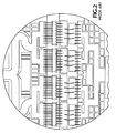
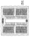
- FIGs. 1 and 2 illustrate two such prior art configurations, Fig. 1 illustrating a device known as the SGS Thompson TH430 and Fig. 2 illustrating a device known as the Toshiba TPM1919.
- the SGS Thompson TH430 shown in Fig. 1 is a four-die bipolar device incorporating a center base feed with the emitters on the outside of the rectangular array. There is no provision in this design for equalizing the path length from the base terminal to the individual die bases. It is believed that the upper frequency of the die, referred to herein as the cutoff frequency of the transistors, is close to the 50MHz upper frequency limit of the four-die device.
- the Toshiba TPM1919 shown in Fig. 2 is a 2GHz device having four MESFET dies in a linear array. It uses an "echelon" divider structure to divide the gate signal four ways. There are matching networks between the gate connections and the ends of the divider structure. It is believed that these matching networks provide impedance transformation at the intended frequency of operation which facilitates implementation of the device.
- the device's input structure provides certain balancing and isolation functions. Its frequency of operation is believed to be near the upper limit of the individual dies.
- the known prior art devices operate at the top end of the dies' frequency capability.
- the prior art gate and/or base wires are necessarily short because of the very high frequencies involved.
- their parasitic resonant (and potential oscillation) frequency is higher than the frequency at which the dies run out of gain. Thus, there is little or no oscillation.
- the Motorola design MRF 154 (Fig. 2') is described in U.S. Patent No. 4,639,760 uses series gate resistors to intentionally substantially reduce the gain of the individual gate cells to substantially prevent oscillation.
- the die has gain response to>500 MHz, but the intended frequency range of the total device was ⁇ 100 MHz. Thus, the Motorola design has excess gain.
- U.S. Patent No. 5,731,970 described a power conversion device, a three-level inverter for driving motors in vehicles and semiconductor module designed to mitigate the adverse effects of high wiring inductance when using many devices.
- U.S. Patent No. 5,731,970 refers to the problem associated with oscillation in the emitter (source)-collector pathway in a multiple power device module and U. S. Patent No. 5,731,970 teaches minimization of impedance, particularly inductance, by making wiring lengths as short as possible, by making them equal with respect to the individual devices and by housing the devices in a module where wiring is replaced by electrode places in order to eliminate inductance and reduce nonuniformity of current among the devices.
- the invention involves a method of packaging and interconnecting plural power transistor dies to operate at a first frequency without oscillation at a second frequency higher than ther first frequency but lower than a cutoff frequency of the transistors.
- the method comprises mounting the dies on a substrate wich a lower side (drain) of each die electrically and thermally bonded to a first area of a conductive layer on the substrate; electrically connecting a source of each die to a second area of the conductive layer on the substrate; and electrically connecting a gate of each die to a third, common interior central area of the conductive layer on the substrate via separate electrical leads.
- the leads are sized to substantially the same electrical length and provide a first impedance corresponding to said electrical length from the common area to each gate chat will pass the first frequency substantially unattenuated and providing a second impedance from the gate of one die to the gate of a second die that will substantially attenuate the second frequency.
- the leads take the form of one or more jumper wires in series with a film resistor.
- they take the form of one or more meandering striplines having predefined impedance characteristics and one or more gate bonding pads connected to their respective gates with long jumper wires.
- the input capacitance of the transistors in accordance with the invention, is high. This high capacitance lowers the resonant frequency of the parasitic structure of the transistors, which can cause oscillation when the transistors are coupled in parallel in a power module. Because of the higher input capacitance and the use of source resistors, in accordance with a first embodiment of the invention, the gain at the intended frequency of operation is not very high to begin with.
- the invention may be seen to provide a reliable, easily and repeatably manufactured, modular configuration of multiple power MOSFET dies designed for RF power applications.
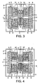
- Fig. 3 illustrates a first embodiment of the invention having balanced gate input connections that utilize printed series resistors.
- a relatively lower gain amplifier is obtained, but one that performs without undesirable oscillation.
- smaller dies having greater gain may be used so that the series resistors do not consume most of the gain margin at the desired operating frequency.
- Fig. 3 shows the four-die (each labeled 1) array mounted on a preferably ceramic (e.g. BeO) substrate 2 providing a conductive source connection area 3, a conductive drain connection area 4 and a conductive gate connection area 5.
- Thin-film source resistors 6 e.g. palladium gold
- Gate bond wires 7 and source bond wires 8 e.g. aluminum
- source bond pads 9 e.g. silver
- Jumper wires 10 e.g. aluminum
- the far ends of gate resistors 13 are wire bonded by gate bond wires 7 to plural corresponding gate connections on each of the dies 1.
- Fig. 4 shows a second embodiment of the invention having balanced gate input connections that utilize printed meandering striplines or stripline connection lines 11 exhibiting a relatively high intrinsic inductance. Because the impedance of the inductive striplines is frequency-dependent (unlike that of the resistors, which is frequency-independent), it is possible to achieve higher gain without oscillation in this second embodiment of the invention. It will be appreciated that the layout topology of the second embodiment is like that of the first: the gates' first off-die connection is to be in a common interior central location therein. Those of skill in the art will appreciate that the striplines also intrinsically have a characteristic resistance and capacitance, however low.
- the meandering striplines are of substantially equal electrical length, i.e. they exhibit nearly identical impedances (including resistance, inductance and capacitance), and extend from an external gate terminal 5' through jumper wires 10 to a central common landing region L' within the die array and between adjacent dies.
- the meandering inductors terminate in gate bonding pads 12' for wire bonding using gate bond wires 7' to the plural corresponding gate pads on each of the dies 1.
- substrate 2, source connection area 3, drain connection area 4, source resistors 6, source bond wires 8 and source bond pads 9 are substantially identical to those of the first embodiment of the invention described above relative to Fig. 3.
- the meandering nature of the striplines effectively electrically lengthens the leads, without substantially increasing the required connection layout area.
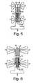
- Fig. 5 is a detailed schematic diagram showing only the gate connection area of the device of Fig. 3.
- Fig. 5 features the above-described gate connection 5 for the device and bond wires 7. It also shows second (central) gate connection bond wires 10 (six in accordance with the first embodiment shown) providing a controlled-impedance (e.g. resistive/inductive/capacitive) path between gate connection 5 and the centrally located gate landing L. It further shows the gate bonding pads 12 (one per die). Finally, it shows preferably printed circuit resistors 13 (also one per die). The number of jumper wires 10 and their lengths may be adjusted to achieve desired inductance, resistance and current capacity for a given application.
- second (central) gate connection bond wires 10 (six in accordance with the first embodiment shown) providing a controlled-impedance (e.g. resistive/inductive/capacitive) path between gate connection 5 and the centrally located gate landing L. It further shows the gate bonding pads 12 (one per die). Finally, it shows preferably
- the gate series resistors are approximately 3 ⁇ or less. Those of skill in the art will appreciate that the series resistance value is selected to effectively suppress oscillation at a given operating frequency of the device, while not reducing the overall gain of the device more than is necessary. Also, as illustrated in the preferred first embodiment, the six thin jumper wires 10 are arranged in parallel.
- Fig. 6 is a detailed schematic diagram showing only the gate connection area of the device of Fig. 4.
- the second embodiment of the invention omits the gate series resistors 13, reconfigures the gate bonding pads 12' to a smaller footprint, and incorporates four controlled-impedance stripline connection lines 11 extending as shown between a common central landing L' and bonding pads 12'.
- the landing L' may be seen to be connected to the gate connection 5' via six parallel jumper wires 10, as in Figs. 3 and 5.
- the typical characteristic impedance of the controlled-impedance striplines--compatible with the selected dies- is approximately 90 ⁇ , as determined by their width and the thickness and dielectric properties of the substrate 2.
- the striplines are approximately 0.65 inch long and 0.013 inch wide, while the substrate is approximately 40 mils thick.
- the input impedance of the dies 1 themselves is less than approximately 0.2 ⁇ .
- the ratio of conductor width to dielectric layer thickness determines the characteristic impedance, and that the length of the conductor determines the series impedance the meandering stripline imparts between the gate and the common connection point L'.
- the illustrated striplines may be differently characterized, formed and/or routed, within the spirit and scope of the invention.
Abstract
Description
- The present invention relates to power modules containing plural transistor dies providing a single external gate terminal. More particularly, it concerns a power module that operates at a first frequency without oscillation at a second higher frequency that is below a cutoff frequency of the transistors.
- Prior art power module devices utilizing plural transistor dies are known. Figs. 1 and 2 illustrate two such prior art configurations, Fig. 1 illustrating a device known as the SGS Thompson TH430 and Fig. 2 illustrating a device known as the Toshiba TPM1919.
- The SGS Thompson TH430 shown in Fig. 1 is a four-die bipolar device incorporating a center base feed with the emitters on the outside of the rectangular array. There is no provision in this design for equalizing the path length from the base terminal to the individual die bases. It is believed that the upper frequency of the die, referred to herein as the cutoff frequency of the transistors, is close to the 50MHz upper frequency limit of the four-die device.
- The Toshiba TPM1919 shown in Fig. 2 is a 2GHz device having four MESFET dies in a linear array. It uses an "echelon" divider structure to divide the gate signal four ways. There are matching networks between the gate connections and the ends of the divider structure. It is believed that these matching networks provide impedance transformation at the intended frequency of operation which facilitates implementation of the device. The device's input structure provides certain balancing and isolation functions. Its frequency of operation is believed to be near the upper limit of the individual dies.
- Accordingly, the known prior art devices operate at the top end of the dies' frequency capability. The prior art gate and/or base wires are necessarily short because of the very high frequencies involved. As a result, their parasitic resonant (and potential oscillation) frequency is higher than the frequency at which the dies run out of gain. Thus, there is little or no oscillation.
- The Motorola design MRF 154 (Fig. 2') is described in U.S. Patent No. 4,639,760 uses series gate resistors to intentionally substantially reduce the gain of the individual gate cells to substantially prevent oscillation. The die has gain response to>500 MHz, but the intended frequency range of the total device was <100 MHz. Thus, the Motorola design has excess gain.
- Furthermore, U.S. Patent No. 5,731,970 described a power conversion device, a three-level inverter for driving motors in vehicles and semiconductor module designed to mitigate the adverse effects of high wiring inductance when using many devices.
- U.S. Patent No. 5,731,970 refers to the problem associated with oscillation in the emitter (source)-collector pathway in a multiple power device module and U. S. Patent No. 5,731,970 teaches minimization of impedance, particularly inductance, by making wiring lengths as short as possible, by making them equal with respect to the individual devices and by housing the devices in a module where wiring is replaced by electrode places in order to eliminate inductance and reduce nonuniformity of current among the devices.
- The invention is defined by the claims.
- The invention involves a method of packaging and interconnecting plural power transistor dies to operate at a first frequency without oscillation at a second frequency higher than ther first frequency but lower than a cutoff frequency of the transistors. The method comprises mounting the dies on a substrate wich a lower side (drain) of each die electrically and thermally bonded to a first area of a conductive layer on the substrate; electrically connecting a source of each die to a second area of the conductive layer on the substrate; and electrically connecting a gate of each die to a third, common interior central area of the conductive layer on the substrate via separate electrical leads.
- The leads are sized to substantially the same electrical length and provide a first impedance corresponding to said electrical length from the common area to each gate chat will pass the first frequency substantially unattenuated and providing a second impedance from the gate of one die to the gate of a second die that will substantially attenuate the second frequency. In accordance with a first embodiment, the leads take the form of one or more jumper wires in series with a film resistor. In accordance with a second embodiment, they take the form of one or more meandering striplines having predefined impedance characteristics and one or more gate bonding pads connected to their respective gates with long jumper wires.
-
- FIG. 1 illustrates prior art power amplifier.
- FIG. 2 illustrates another prior art power amplifier.
- FIG. 2' illustrates a third prior art power amplifier.
- FIG. 3 is a schematic diagram of a first embodiment of the present invention.
- FIG. 4 is a schematic diagram of a second embodiment of the present invention.
- FIG. 5 is a more detailed schematic diagram of the gate structure of the embodiment shown in FIG. 3.
- FIG. 6 is a more detailed schematic diagram of the gate structure of the embodiment shown in FIG. 4.
- In accordance with the present invention, four power MOSFET transistor dies are arranged in a rectangular, e.g. a square, array, as shown in Figs. 3 and 4. The dies have an upper limit of 250 MHz, but they are twice as large as the dies in the Motorola design. As a result, the input capacitance of the transistors, in accordance with the invention, is high. This high capacitance lowers the resonant frequency of the parasitic structure of the transistors, which can cause oscillation when the transistors are coupled in parallel in a power module. Because of the higher input capacitance and the use of source resistors, in accordance with a first embodiment of the invention, the gain at the intended frequency of operation is not very high to begin with. Thus, there is little excess gain, and the gate resistors alone decrease overall amplifier gain. If the resistance needed to suppress oscillation is too high, then inductors may be used instead. Thus a second embodiment of the invention utilizes gate inductors instead of gate resistors, and provides higher gain without oscillation.
- The invention may be seen to provide a reliable, easily and repeatably manufactured, modular configuration of multiple power MOSFET dies designed for RF power applications.
- Fig. 3 illustrates a first embodiment of the invention having balanced gate input connections that utilize printed series resistors. Those of skill in the art will appreciate that, in this first embodiment, a relatively lower gain amplifier is obtained, but one that performs without undesirable oscillation. Those of skill also will appreciate that, to increase the gain of such an amplifier embodiment, smaller dies having greater gain may be used so that the series resistors do not consume most of the gain margin at the desired operating frequency.
- Fig. 3 shows the four-die (each labeled 1) array mounted on a preferably ceramic (e.g. BeO)
substrate 2 providing a conductivesource connection area 3, a conductivedrain connection area 4 and a conductivegate connection area 5. Thin-film source resistors 6 (e.g. palladium gold) are located on the substrate outside the perimeter of the die array.Gate bond wires 7 and source bond wires 8 (e.g. aluminum), as well as source bond pads 9 (e.g. silver) are provided, as shown. Jumper wires 10 (e.g. aluminum) extend fromgate connection area 5 to a centrally located gate landing L adjacent and electrically connected togate series resistors 13. The far ends ofgate resistors 13 are wire bonded bygate bond wires 7 to plural corresponding gate connections on each of the dies 1. - Fig. 4 shows a second embodiment of the invention having balanced gate input connections that utilize printed meandering striplines or
stripline connection lines 11 exhibiting a relatively high intrinsic inductance. Because the impedance of the inductive striplines is frequency-dependent (unlike that of the resistors, which is frequency-independent), it is possible to achieve higher gain without oscillation in this second embodiment of the invention. It will be appreciated that the layout topology of the second embodiment is like that of the first: the gates' first off-die connection is to be in a common interior central location therein. Those of skill in the art will appreciate that the striplines also intrinsically have a characteristic resistance and capacitance, however low. - It may be seen from Fig. 4 that the meandering striplines are of substantially equal electrical length, i.e. they exhibit nearly identical impedances (including resistance, inductance and capacitance), and extend from an external gate terminal 5' through
jumper wires 10 to a central common landing region L' within the die array and between adjacent dies. The meandering inductors terminate in gate bonding pads 12' for wire bonding using gate bond wires 7' to the plural corresponding gate pads on each of the dies 1. It will be understood thatsubstrate 2,source connection area 3,drain connection area 4,source resistors 6,source bond wires 8 andsource bond pads 9 are substantially identical to those of the first embodiment of the invention described above relative to Fig. 3. Those of skill in the art will appreciate that the meandering nature of the striplines effectively electrically lengthens the leads, without substantially increasing the required connection layout area. - Fig. 5 is a detailed schematic diagram showing only the gate connection area of the device of Fig. 3. Fig. 5 features the above-described
gate connection 5 for the device andbond wires 7. It also shows second (central) gate connection bond wires 10 (six in accordance with the first embodiment shown) providing a controlled-impedance (e.g. resistive/inductive/capacitive) path betweengate connection 5 and the centrally located gate landing L. It further shows the gate bonding pads 12 (one per die). Finally, it shows preferably printed circuit resistors 13 (also one per die). The number ofjumper wires 10 and their lengths may be adjusted to achieve desired inductance, resistance and current capacity for a given application. - In accordance with a preferred first embodiment, the gate series resistors are approximately 3Ω or less. Those of skill in the art will appreciate that the series resistance value is selected to effectively suppress oscillation at a given operating frequency of the device, while not reducing the overall gain of the device more than is necessary. Also, as illustrated in the preferred first embodiment, the six
thin jumper wires 10 are arranged in parallel. - Fig. 6 is a detailed schematic diagram showing only the gate connection area of the device of Fig. 4. As described above with reference to Fig. 4, the second embodiment of the invention omits the
gate series resistors 13, reconfigures the gate bonding pads 12' to a smaller footprint, and incorporates four controlled-impedancestripline connection lines 11 extending as shown between a common central landing L' and bonding pads 12'. The landing L' may be seen to be connected to the gate connection 5' via sixparallel jumper wires 10, as in Figs. 3 and 5. - The typical characteristic impedance of the controlled-impedance striplines--compatible with the selected dies-is approximately 90Ω, as determined by their width and the thickness and dielectric properties of the
substrate 2. In accordance with the second embodiment of the invention described above by reference to Figs. 4 and 6, the striplines are approximately 0.65 inch long and 0.013 inch wide, while the substrate is approximately 40 mils thick. The input impedance of the dies 1 themselves is less than approximately 0.2Ω. - Those of skill in the art will appreciate that the ratio of conductor width to dielectric layer thickness determines the characteristic impedance, and that the length of the conductor determines the series impedance the meandering stripline imparts between the gate and the common connection point L'. Those of skill in the art also will appreciate that the illustrated striplines may be differently characterized, formed and/or routed, within the spirit and scope of the invention.
- For purpose of description, a rectangular array of four-die is represented. Other geometric arrangements, circular, triangular, etc., with more or less die could also be used with the method described, and are within the spirit and scope of the invention.
- Accordingly, having illustrated and described the principles of our invention in a preferred embodiment thereof, it should be readily apparent to those skilled in the art that the invention can be modified in arrangement and detail without departing from such principles. We claim all modifications coming within the scope of the accompanying claims.
Claims (16)
- A method of packaging and interconnecting plural power transistor dies to operate at a first frequency without oscillation at a second frequency higher than the first frequency but lower than a cutoff frequency of the transistors, the method comprising:mounting the dies (1) on a substrate (2) with a lower side (drain) of each die electrically and thermally bonded to a first area (4) of a conductive layer on the substrate;electrically connecting a source of each die to a second area (3) of the conductive layer on the substrate; andelectrically connecting 4 gate of each die to a third, common, interior central landing area (L, L') of the conductive layer on the substrate via separate electrical leads, characterised in thatthe leads extend from said third, common, interior central landing area (L,L') to each of the gates of said dies and are sized to substantially the same electrical length and provide a first impedance corresponding to said electrical length from the common area (L, L') to each gate that will pass the first frequency substantially unattenuated and provide a second impedance from the gate of one die to the gate of a second die that will substantially attenuate the second frequency.
- A method according to claim 1, wherein the plural dies (1) are arranged in an array, and the substrate (2) is arranged so that the second area (3) coupled to the sources is positioned outside the array and the third area (L, L') is interior and central to the array and between the dies.
- A method according to claim 1, wherein the plural dies (1) are arranged in an array, which further comprises a set of conductive first jumper wires (10) connecting the third area (L, L') to a fourth area (5, 5'), and wherein the substrate (2) is arranged so that the second area (3) coupled to the sources is positioned outside of the array on opposite first and second sides, the third area (L, L') is positioned approximately centrally within the array and the fourth area (5, 5') is substantially outside the array.
- A method according to claim 1, wherein the leads each include a first portion (11,13) extending from the third area (L, L') to a gate pad (12, 12') corresponding to the gate of the respective die, the first portion including one or more controlled-impedance films, a second portion connected in series with the first portion, the second portion including the gate pad (12,12') and a third portion connected in series with the second portion, the third portion including one or more conductive jumpers (7, 7') extending to the gate of the respective die.
- A method according to claim 4, wherein at least the first and second portions (11, 13; 12, 12') of the leads are integrally formed in the conductive layer so as to delineate lines of substantially equal, defined impedance on the substrate having substantially equal resistance, inductance and capacitance, and wherein the conductive jumpers (7, 7') are configured to be of substantially equal, defined impedance coupling each gate pad to the respective gate.
- A method according to claim 1, wherein the leads each include a first portion (11) that is integrally formed in the conductive layer and that extends between the third area (L') and gate pad (12') corresponding with one of the dies (1), the first portion taking the form of a meandering stripline (11), and wherein the leads each include a second portion that includes a first set of plural conductive jumpers (7') configured to be of substantially equal, defined impedance coupling each gate pad to the respective gate.
- The method of claim 6, wherein the plural dies (I) are arranged in an array, which further comprises a set of conductive first jumper wires (10) connecting the third area (L') to a fourth area (5'), and wherein the substrate is arranged so that the second area (3) coupled to the sources is positioned outside of the array on opposite first and second sides, the third area (L') is positioned approximately centrally within the array and the fourth area (5') is substantially outside the array.
- The method of claims 2, 3, or 7, wherein the array is rectangular.
- A power module packaging and interconnecting plural power transistor dies to operate at a first frequency without oscillation at a second frequency higher than the first frequency but lower than a cutoff frequency of the transistors, the module comprising:a substrate (2) having a conductive layer patterned to form a first area (4), a second area (3), and a third, common, interior central landing area (L, L');plural power transistors dies (1) mounted on the substrate with a lower side (drain) of each die electrically and thermally bonded to the first area (4) of the conductive layer on the substrate;a source of each die electrically connected to the second area (3) of the conductive layer on the substrate; and,a gate of each die (1) electrically connected to the third, common, interior central landing area (L, L') of the conductive layer on the substrate via separate electrical leads, characterised in thatthe leads extend from said third, common, interior central landing area (L,L') to each of the gates of said dies and are sized to substantially the same electrical length and provide a first impedance corresponding to said electrical length from the common area (L, L') to each gate that will pass the first frequency substantially unattenuated and provide a second impedance from the gate of one die to the gate of a second die that will substantially attenuate the second frequency.
- A power module according to claim 9, wherein the plural dies (1) are arranged in an array, and the substrate (2) is arranged so that the second area (3) coupled to the sources is positioned outside the array and the third area (L, L') is interior and central to the array and between the dies.
- A power module according to claim 9, wherein the plural dies (1) are arranged in an array, which further comprises a set of conductive first jumper wires (10) connecting the third area (L, L') to a fourth area (5, 5'), and wherein the substrate (2) is arranged so that the second area (3) coupled to the sources is positioned outside of the array on opposite first and second sides, the third area (L, L') is positioned approximately centrally within the array and the fourth area (5, 5') is substantially outside the array.
- A power module according to claim 9, wherein the leads each include a first portion (11, 13) extending from the third area (L, L') to a gate pad (12,12') corresponding to the gate of a respective die, the first portion including one or more controlled-impedance films, a second portion connected in series with the first portion, the second portion including the gate pad (12, 12') and a third portion connected in series with the second portion, the third portion including one or more conductive jumpers (7, 7') extending to the gate of the respective die.
- A power module according to claim 12, wherein at least the first and second portions (11, 13; 12,12') of the leads are integrally formed in the conductive layer so as to delineate lines of substantially equal, defined impedance on the substrate having substantially equal resistance, inductance and capacitance, and wherein the conductive jumpers (7, 7') are configured to be of substantially equal, defined impedance coupling each gate pad to a respective gate.
- A power module according to claim 9, wherein the leads each include a first portion (11) that is integrally formed in the conductive layer and that extends between the third area (L') and gate pad (12') corresponding with one of the dies (1), the first portion taking the form of a meandering stripline (11), and wherein the leads each include a second portion that includes a first set of plural conductive jumpers (7') configured to be of substantially equal, defined impedance coupling each gate pad to the respective gate.
- The power module of claim 14, wherein the plural dies (1) are arranged in an array, which further comprises a set of conductive first jumper wires (10) connecting the third area (L') to a fourth area (5'), and wherein the substrate is arranged so that the second area (3) coupled to the sources is positioned outside of the array on opposite first and second sides, the third area (L') is positioned approximately centrally within the array and the fourth area (5') is substantially outside the array.
- The power module of claims 10,11 or 15, wherein the array is rectangular.
Applications Claiming Priority (3)
| Application Number | Priority Date | Filing Date | Title |
|---|---|---|---|
| US35380902P | 2002-01-29 | 2002-01-29 | |
| US353809P | 2002-01-29 | ||
| PCT/US2003/002326 WO2003065454A2 (en) | 2002-01-29 | 2003-01-27 | Split-gate power module and method for suppressing oscillation therein |
Publications (2)
| Publication Number | Publication Date |
|---|---|
| EP1470588A2 EP1470588A2 (en) | 2004-10-27 |
| EP1470588B1 true EP1470588B1 (en) | 2006-09-06 |
Family
ID=27663256
Family Applications (1)
| Application Number | Title | Priority Date | Filing Date |
|---|---|---|---|
| EP03705914A Expired - Lifetime EP1470588B1 (en) | 2002-01-29 | 2003-01-27 | Split-gate power module and method for suppressing oscillation therein |
Country Status (8)
| Country | Link |
|---|---|
| US (2) | US6939743B2 (en) |
| EP (1) | EP1470588B1 (en) |
| JP (1) | JP4732692B2 (en) |
| KR (1) | KR20040085169A (en) |
| CN (1) | CN100380661C (en) |
| AT (1) | ATE339013T1 (en) |
| DE (1) | DE60308148T2 (en) |
| WO (1) | WO2003065454A2 (en) |
Cited By (1)
| Publication number | Priority date | Publication date | Assignee | Title |
|---|---|---|---|---|
| EP4047818A4 (en) * | 2019-10-15 | 2023-11-22 | Kyosan Electric Mfg. Co., Ltd. | Switching module |
Families Citing this family (10)
| Publication number | Priority date | Publication date | Assignee | Title |
|---|---|---|---|---|
| JP4342232B2 (en) * | 2003-07-11 | 2009-10-14 | 三菱電機株式会社 | Semiconductor power module and main circuit current measuring system for measuring main circuit current value of the module |
| GB201105912D0 (en) * | 2011-04-07 | 2011-05-18 | Diamond Microwave Devices Ltd | Improved matching techniques for power transistors |
| US8581660B1 (en) * | 2012-04-24 | 2013-11-12 | Texas Instruments Incorporated | Power transistor partial current sensing for high precision applications |
| CN104380463B (en) * | 2012-06-19 | 2017-05-10 | Abb 技术有限公司 | Substrate for mounting multiple power transistors thereon and power semiconductor module |
| DE102014111931B4 (en) * | 2014-08-20 | 2021-07-08 | Infineon Technologies Ag | Low-inductance circuit arrangement with load current busbar |
| WO2018109069A1 (en) | 2016-12-16 | 2018-06-21 | Abb Schweiz Ag | Power semiconductor module with low gate path inductance |
| JP6838243B2 (en) | 2017-09-29 | 2021-03-03 | 日立Astemo株式会社 | Power converter |
| DE102019112935B4 (en) | 2019-05-16 | 2021-04-29 | Danfoss Silicon Power Gmbh | Semiconductor module |
| JP7351209B2 (en) | 2019-12-17 | 2023-09-27 | 富士電機株式会社 | semiconductor equipment |
| JP2021097146A (en) | 2019-12-18 | 2021-06-24 | 富士電機株式会社 | Semiconductor device |
Family Cites Families (16)
| Publication number | Priority date | Publication date | Assignee | Title |
|---|---|---|---|---|
| US4639760A (en) * | 1986-01-21 | 1987-01-27 | Motorola, Inc. | High power RF transistor assembly |
| US4907068A (en) * | 1987-01-21 | 1990-03-06 | Siemens Aktiengesellschaft | Semiconductor arrangement having at least one semiconductor body |
| JP2751707B2 (en) * | 1992-01-29 | 1998-05-18 | 株式会社日立製作所 | Semiconductor module and power conversion device using the same |
| US5731970A (en) * | 1989-12-22 | 1998-03-24 | Hitachi, Ltd. | Power conversion device and semiconductor module suitable for use in the device |
| JPH04183001A (en) * | 1990-11-16 | 1992-06-30 | Mitsubishi Electric Corp | Package for microwave ic |
| JPH0575314A (en) * | 1991-09-13 | 1993-03-26 | Matsushita Electron Corp | Microwave integrated circuit element |
| JP3053298B2 (en) * | 1992-08-19 | 2000-06-19 | 株式会社東芝 | Semiconductor device |
| DE59304797D1 (en) * | 1992-08-26 | 1997-01-30 | Eupec Gmbh & Co Kg | Power semiconductor module |
| US6291878B1 (en) * | 1993-04-22 | 2001-09-18 | Sundstrand Corporation | Package for multiple high power electrical components |
| JP2973799B2 (en) * | 1993-04-23 | 1999-11-08 | 富士電機株式会社 | Power transistor module |
| US5563447A (en) * | 1993-09-07 | 1996-10-08 | Delco Electronics Corp. | High power semiconductor switch module |
| DE19644009A1 (en) * | 1996-10-31 | 1998-05-07 | Siemens Ag | Large-area high-current module of a field-controlled, switchable power semiconductor switch |
| JP2000323647A (en) * | 1999-05-12 | 2000-11-24 | Toshiba Corp | Module semiconductor device and manufacture thereof |
| JP4163818B2 (en) * | 1999-07-07 | 2008-10-08 | 三菱電機株式会社 | Internally matched transistor |
| JP4138192B2 (en) * | 1999-12-27 | 2008-08-20 | 三菱電機株式会社 | Semiconductor switch device |
| US6617679B2 (en) * | 2002-02-08 | 2003-09-09 | Advanced Energy Industries, Inc. | Semiconductor package for multiple high power transistors |
-
2003
- 2003-01-27 WO PCT/US2003/002326 patent/WO2003065454A2/en active IP Right Grant
- 2003-01-27 KR KR10-2004-7011632A patent/KR20040085169A/en not_active Application Discontinuation
- 2003-01-27 JP JP2003564937A patent/JP4732692B2/en not_active Expired - Lifetime
- 2003-01-27 CN CNB03802909XA patent/CN100380661C/en not_active Expired - Fee Related
- 2003-01-27 AT AT03705914T patent/ATE339013T1/en not_active IP Right Cessation
- 2003-01-27 DE DE60308148T patent/DE60308148T2/en not_active Expired - Fee Related
- 2003-01-27 EP EP03705914A patent/EP1470588B1/en not_active Expired - Lifetime
- 2003-01-27 US US10/352,314 patent/US6939743B2/en not_active Expired - Lifetime
-
2005
- 2005-06-03 US US11/145,042 patent/US7342262B2/en not_active Expired - Lifetime
Cited By (1)
| Publication number | Priority date | Publication date | Assignee | Title |
|---|---|---|---|---|
| EP4047818A4 (en) * | 2019-10-15 | 2023-11-22 | Kyosan Electric Mfg. Co., Ltd. | Switching module |
Also Published As
| Publication number | Publication date |
|---|---|
| JP4732692B2 (en) | 2011-07-27 |
| EP1470588A2 (en) | 2004-10-27 |
| WO2003065454A2 (en) | 2003-08-07 |
| WO2003065454A3 (en) | 2004-02-26 |
| CN1625807A (en) | 2005-06-08 |
| US7342262B2 (en) | 2008-03-11 |
| ATE339013T1 (en) | 2006-09-15 |
| CN100380661C (en) | 2008-04-09 |
| DE60308148T2 (en) | 2007-08-16 |
| KR20040085169A (en) | 2004-10-07 |
| US20030141587A1 (en) | 2003-07-31 |
| DE60308148D1 (en) | 2006-10-19 |
| US20050218500A1 (en) | 2005-10-06 |
| JP2006502560A (en) | 2006-01-19 |
| US6939743B2 (en) | 2005-09-06 |
Similar Documents
| Publication | Publication Date | Title |
|---|---|---|
| US7342262B2 (en) | Split-gate power module for suppressing oscillation therein | |
| EP1573813B1 (en) | Rf power transistor with internal bias feed | |
| US8487407B2 (en) | Low impedance gate control method and apparatus | |
| US8228113B2 (en) | Power semiconductor module and method for operating a power semiconductor module | |
| US6636429B2 (en) | EMI reduction in power modules through the use of integrated capacitors on the substrate level | |
| EP1160866B1 (en) | Semiconductor device with power wiring structure | |
| EP3160042A1 (en) | Rf power transistors with video bandwidth circuits, and methods of manufacture thereof | |
| US8592966B2 (en) | RF transistor packages with internal stability network including intra-capacitor resistors and methods of forming RF transistor packages with internal stability networks including intra-capacitor resistors | |
| JP2014057304A (en) | Semiconductor devices with impedance matching-circuits, and methods of manufacture thereof | |
| WO2017163612A1 (en) | Power semiconductor module | |
| KR20010080542A (en) | High frequency power transistor divice | |
| EP2879174A1 (en) | Packaged RF power transistor device having next to each other a ground and a video lead for connecting a decoupling capacitor, RF power amplifier | |
| US6384492B1 (en) | Power semiconductor packaging | |
| EP0544387B1 (en) | High gain monolithic microwave integrated circuit amplifier | |
| US6777791B2 (en) | Multiple ground signal path LDMOS power package | |
| US7019362B2 (en) | Power MOSFET with reduced dgate resistance | |
| US5027192A (en) | Fast power semiconductor circuit | |
| US4975659A (en) | Amplifier package using vertical power transistors with ungrounded common terminals | |
| US20220139797A1 (en) | Semiconductor module, power semiconductor module, and power electronic equipment using the semiconductor module or the power semiconductor module | |
| US6624703B1 (en) | Terminal arrangement for an electrical device | |
| US20220102291A1 (en) | Power module | |
| WO2023043686A1 (en) | Bridged class-d rf amplifier circuit | |
| US20120132969A1 (en) | Compensation network for rf transistor | |
| WO2022058313A1 (en) | Molded resin power module | |
| JPS647682B2 (en) |
Legal Events
| Date | Code | Title | Description |
|---|---|---|---|
| PUAI | Public reference made under article 153(3) epc to a published international application that has entered the european phase |
Free format text: ORIGINAL CODE: 0009012 |
|
| 17P | Request for examination filed |
Effective date: 20040630 |
|
| AK | Designated contracting states |
Kind code of ref document: A2 Designated state(s): AT BE BG CH CY CZ DE DK EE ES FI FR GB GR HU IE IT LI LU MC NL PT SE SI SK TR |
|
| AX | Request for extension of the european patent |
Extension state: AL LT LV MK RO |
|
| 17Q | First examination report despatched |
Effective date: 20041223 |
|
| GRAP | Despatch of communication of intention to grant a patent |
Free format text: ORIGINAL CODE: EPIDOSNIGR1 |
|
| GRAS | Grant fee paid |
Free format text: ORIGINAL CODE: EPIDOSNIGR3 |
|
| GRAA | (expected) grant |
Free format text: ORIGINAL CODE: 0009210 |
|
| AK | Designated contracting states |
Kind code of ref document: B1 Designated state(s): AT BE BG CH CY CZ DE DK EE ES FI FR GB GR HU IE IT LI LU MC NL PT SE SI SK TR |
|
| PG25 | Lapsed in a contracting state [announced via postgrant information from national office to epo] |
Ref country code: IT Free format text: LAPSE BECAUSE OF FAILURE TO SUBMIT A TRANSLATION OF THE DESCRIPTION OR TO PAY THE FEE WITHIN THE PRESCRIBED TIME-LIMIT;WARNING: LAPSES OF ITALIAN PATENTS WITH EFFECTIVE DATE BEFORE 2007 MAY HAVE OCCURRED AT ANY TIME BEFORE 2007. THE CORRECT EFFECTIVE DATE MAY BE DIFFERENT FROM THE ONE RECORDED. Effective date: 20060906 Ref country code: SI Free format text: LAPSE BECAUSE OF FAILURE TO SUBMIT A TRANSLATION OF THE DESCRIPTION OR TO PAY THE FEE WITHIN THE PRESCRIBED TIME-LIMIT Effective date: 20060906 Ref country code: SK Free format text: LAPSE BECAUSE OF FAILURE TO SUBMIT A TRANSLATION OF THE DESCRIPTION OR TO PAY THE FEE WITHIN THE PRESCRIBED TIME-LIMIT Effective date: 20060906 Ref country code: CZ Free format text: LAPSE BECAUSE OF FAILURE TO SUBMIT A TRANSLATION OF THE DESCRIPTION OR TO PAY THE FEE WITHIN THE PRESCRIBED TIME-LIMIT Effective date: 20060906 Ref country code: LI Free format text: LAPSE BECAUSE OF FAILURE TO SUBMIT A TRANSLATION OF THE DESCRIPTION OR TO PAY THE FEE WITHIN THE PRESCRIBED TIME-LIMIT Effective date: 20060906 Ref country code: BE Free format text: LAPSE BECAUSE OF FAILURE TO SUBMIT A TRANSLATION OF THE DESCRIPTION OR TO PAY THE FEE WITHIN THE PRESCRIBED TIME-LIMIT Effective date: 20060906 Ref country code: AT Free format text: LAPSE BECAUSE OF FAILURE TO SUBMIT A TRANSLATION OF THE DESCRIPTION OR TO PAY THE FEE WITHIN THE PRESCRIBED TIME-LIMIT Effective date: 20060906 Ref country code: FI Free format text: LAPSE BECAUSE OF FAILURE TO SUBMIT A TRANSLATION OF THE DESCRIPTION OR TO PAY THE FEE WITHIN THE PRESCRIBED TIME-LIMIT Effective date: 20060906 Ref country code: CH Free format text: LAPSE BECAUSE OF FAILURE TO SUBMIT A TRANSLATION OF THE DESCRIPTION OR TO PAY THE FEE WITHIN THE PRESCRIBED TIME-LIMIT Effective date: 20060906 |
|
| REG | Reference to a national code |
Ref country code: GB Ref legal event code: FG4D |
|
| REG | Reference to a national code |
Ref country code: CH Ref legal event code: EP |
|
| REG | Reference to a national code |
Ref country code: IE Ref legal event code: FG4D |
|
| REF | Corresponds to: |
Ref document number: 60308148 Country of ref document: DE Date of ref document: 20061019 Kind code of ref document: P |
|
| PG25 | Lapsed in a contracting state [announced via postgrant information from national office to epo] |
Ref country code: SE Free format text: LAPSE BECAUSE OF FAILURE TO SUBMIT A TRANSLATION OF THE DESCRIPTION OR TO PAY THE FEE WITHIN THE PRESCRIBED TIME-LIMIT Effective date: 20061206 Ref country code: DK Free format text: LAPSE BECAUSE OF FAILURE TO SUBMIT A TRANSLATION OF THE DESCRIPTION OR TO PAY THE FEE WITHIN THE PRESCRIBED TIME-LIMIT Effective date: 20061206 Ref country code: BG Free format text: LAPSE BECAUSE OF FAILURE TO SUBMIT A TRANSLATION OF THE DESCRIPTION OR TO PAY THE FEE WITHIN THE PRESCRIBED TIME-LIMIT Effective date: 20061206 |
|
| PG25 | Lapsed in a contracting state [announced via postgrant information from national office to epo] |
Ref country code: ES Free format text: LAPSE BECAUSE OF FAILURE TO SUBMIT A TRANSLATION OF THE DESCRIPTION OR TO PAY THE FEE WITHIN THE PRESCRIBED TIME-LIMIT Effective date: 20061217 |
|
| PG25 | Lapsed in a contracting state [announced via postgrant information from national office to epo] |
Ref country code: MC Free format text: LAPSE BECAUSE OF NON-PAYMENT OF DUE FEES Effective date: 20070131 |
|
| PG25 | Lapsed in a contracting state [announced via postgrant information from national office to epo] |
Ref country code: PT Free format text: LAPSE BECAUSE OF FAILURE TO SUBMIT A TRANSLATION OF THE DESCRIPTION OR TO PAY THE FEE WITHIN THE PRESCRIBED TIME-LIMIT Effective date: 20070219 |
|
| REG | Reference to a national code |
Ref country code: CH Ref legal event code: PL |
|
| ET | Fr: translation filed | ||
| PLBE | No opposition filed within time limit |
Free format text: ORIGINAL CODE: 0009261 |
|
| STAA | Information on the status of an ep patent application or granted ep patent |
Free format text: STATUS: NO OPPOSITION FILED WITHIN TIME LIMIT |
|
| 26N | No opposition filed |
Effective date: 20070607 |
|
| PG25 | Lapsed in a contracting state [announced via postgrant information from national office to epo] |
Ref country code: IE Free format text: LAPSE BECAUSE OF NON-PAYMENT OF DUE FEES Effective date: 20070129 |
|
| PG25 | Lapsed in a contracting state [announced via postgrant information from national office to epo] |
Ref country code: GR Free format text: LAPSE BECAUSE OF FAILURE TO SUBMIT A TRANSLATION OF THE DESCRIPTION OR TO PAY THE FEE WITHIN THE PRESCRIBED TIME-LIMIT Effective date: 20061207 |
|
| PG25 | Lapsed in a contracting state [announced via postgrant information from national office to epo] |
Ref country code: EE Free format text: LAPSE BECAUSE OF FAILURE TO SUBMIT A TRANSLATION OF THE DESCRIPTION OR TO PAY THE FEE WITHIN THE PRESCRIBED TIME-LIMIT Effective date: 20060906 |
|
| REG | Reference to a national code |
Ref country code: GB Ref legal event code: 732E |
|
| NLS | Nl: assignments of ep-patents |
Owner name: MICROSEMI CORPORATION Effective date: 20080704 |
|
| REG | Reference to a national code |
Ref country code: FR Ref legal event code: TP |
|
| PGFP | Annual fee paid to national office [announced via postgrant information from national office to epo] |
Ref country code: DE Payment date: 20090123 Year of fee payment: 7 Ref country code: NL Payment date: 20090104 Year of fee payment: 7 |
|
| PGFP | Annual fee paid to national office [announced via postgrant information from national office to epo] |
Ref country code: GB Payment date: 20090121 Year of fee payment: 7 |
|
| PG25 | Lapsed in a contracting state [announced via postgrant information from national office to epo] |
Ref country code: CY Free format text: LAPSE BECAUSE OF FAILURE TO SUBMIT A TRANSLATION OF THE DESCRIPTION OR TO PAY THE FEE WITHIN THE PRESCRIBED TIME-LIMIT Effective date: 20060906 Ref country code: LU Free format text: LAPSE BECAUSE OF NON-PAYMENT OF DUE FEES Effective date: 20070127 |
|
| PG25 | Lapsed in a contracting state [announced via postgrant information from national office to epo] |
Ref country code: TR Free format text: LAPSE BECAUSE OF FAILURE TO SUBMIT A TRANSLATION OF THE DESCRIPTION OR TO PAY THE FEE WITHIN THE PRESCRIBED TIME-LIMIT Effective date: 20060906 Ref country code: HU Free format text: LAPSE BECAUSE OF FAILURE TO SUBMIT A TRANSLATION OF THE DESCRIPTION OR TO PAY THE FEE WITHIN THE PRESCRIBED TIME-LIMIT Effective date: 20070307 |
|
| PGFP | Annual fee paid to national office [announced via postgrant information from national office to epo] |
Ref country code: FR Payment date: 20090113 Year of fee payment: 7 |
|
| REG | Reference to a national code |
Ref country code: NL Ref legal event code: V1 Effective date: 20100801 |
|
| GBPC | Gb: european patent ceased through non-payment of renewal fee |
Effective date: 20100127 |
|
| REG | Reference to a national code |
Ref country code: FR Ref legal event code: ST Effective date: 20100930 |
|
| PG25 | Lapsed in a contracting state [announced via postgrant information from national office to epo] |
Ref country code: FR Free format text: LAPSE BECAUSE OF NON-PAYMENT OF DUE FEES Effective date: 20100201 Ref country code: NL Free format text: LAPSE BECAUSE OF NON-PAYMENT OF DUE FEES Effective date: 20100801 |
|
| PG25 | Lapsed in a contracting state [announced via postgrant information from national office to epo] |
Ref country code: DE Free format text: LAPSE BECAUSE OF NON-PAYMENT OF DUE FEES Effective date: 20100803 |
|
| PG25 | Lapsed in a contracting state [announced via postgrant information from national office to epo] |
Ref country code: GB Free format text: LAPSE BECAUSE OF NON-PAYMENT OF DUE FEES Effective date: 20100127 |