JP4815491B2 - Integrated DMA - Google Patents
Integrated DMA Download PDFInfo
- Publication number
- JP4815491B2 JP4815491B2 JP2008533662A JP2008533662A JP4815491B2 JP 4815491 B2 JP4815491 B2 JP 4815491B2 JP 2008533662 A JP2008533662 A JP 2008533662A JP 2008533662 A JP2008533662 A JP 2008533662A JP 4815491 B2 JP4815491 B2 JP 4815491B2
- Authority
- JP
- Japan
- Prior art keywords
- dma
- data
- descriptor
- controller
- transfer
- Prior art date
- Legal status (The legal status is an assumption and is not a legal conclusion. Google has not performed a legal analysis and makes no representation as to the accuracy of the status listed.)
- Expired - Fee Related
Links
Images


Classifications
-
- G—PHYSICS
- G06—COMPUTING; CALCULATING OR COUNTING
- G06F—ELECTRIC DIGITAL DATA PROCESSING
- G06F13/00—Interconnection of, or transfer of information or other signals between, memories, input/output devices or central processing units
- G06F13/14—Handling requests for interconnection or transfer
- G06F13/20—Handling requests for interconnection or transfer for access to input/output bus
- G06F13/28—Handling requests for interconnection or transfer for access to input/output bus using burst mode transfer, e.g. direct memory access DMA, cycle steal
Landscapes
- Engineering & Computer Science (AREA)
- Theoretical Computer Science (AREA)
- Physics & Mathematics (AREA)
- General Engineering & Computer Science (AREA)
- General Physics & Mathematics (AREA)
- Bus Control (AREA)
- Information Transfer Systems (AREA)
- Computer And Data Communications (AREA)
- Memory System Of A Hierarchy Structure (AREA)
Abstract
Description
本発明は、集積回路の分野に関し、より具体的には、1つ又は複数の集積回路を備えるシステム内のダイレクト・メモリ・アクセス(DMA)に関する。 The present invention relates to the field of integrated circuits, and more particularly to direct memory access (DMA) in systems comprising one or more integrated circuits.
1つ又は複数のプロセッサ、メモリ、入力/出力(I/O)デバイス、又はインターフェースを含む一般的なシステムでは、I/Oとメモリとの間でデータを転送するためダイレクト・メモリ・アクセス(DMA)転送が利用されることが多い。あるシステムでは、DMAを使用する各I/Oデバイス又はインターフェース内に個々のDMA回路が含まれている。別のシステムでは、1つ又は複数のI/OデバイスがDMA回路を共用している。 In a typical system that includes one or more processors, memory, input / output (I / O) devices, or interfaces, direct memory access (DMA) is used to transfer data between the I / O and the memory. ) Transfer is often used. In some systems, an individual DMA circuit is included within each I / O device or interface that uses DMA. In another system, one or more I / O devices share a DMA circuit.
あるシステムはさらに、1つの記憶領域から別の記憶領域へとデータをコピーするために使用可能な「データ・ムーバ」をも含んでいる。データ・ムーバは、プロセッサをオフロードできるがそうでない場合は、プロセッサはデータ移動(例えば、一般的には一度に32ビット又は64ビットであるプロセッサが使用するビット幅でのデータの読み出しと書き込み)を行う命令を実行しなければならない。データ・ムーバ用のプログラミング・モデルは一般的には、I/Oデバイスとメモリとの間の通信に対応するDMAプログラミング・モデルとは異なっている。 Some systems also include a “data mover” that can be used to copy data from one storage area to another. The data mover can offload the processor, otherwise the processor moves the data (eg, reading and writing data in the bit width used by the processor, typically 32 or 64 bits at a time) You must execute an instruction that performs The programming model for the data mover is generally different from the DMA programming model that supports communication between I / O devices and memory.
一実施態様において、装置は第1のインターフェース回路と、第1のインターフェース回路に結合されたダイレクト・メモリ・アクセス(DMA)コントローラと、DMAコントローラに結合されたホストとを備えている。第1のインターフェース回路はプロトコルに従ってインターフェースで通信するように構成されている。ホストは、ホストのメモリ・システム内の複数の記憶領域に少なくとも一部がマッピングされる少なくとも1つのアドレス空間を備えている。DMAコントローラは、第1のインターフェース回路とアドレス空間との間でDMA転送を行うように構成され、DMAコントローラはさらに、複数の記憶領域のうちの第1の複数の記憶領域と、複数の記憶領域のうちの第2の複数の記憶領域との間でDMA転送を行うように構成されている。方法も企図される。 In one embodiment, the apparatus comprises a first interface circuit, a direct memory access (DMA) controller coupled to the first interface circuit, and a host coupled to the DMA controller. The first interface circuit is configured to communicate with the interface according to a protocol. The host includes at least one address space that is at least partially mapped to a plurality of storage areas in the host's memory system. The DMA controller is configured to perform DMA transfer between the first interface circuit and the address space, and the DMA controller further includes a first plurality of storage areas of the plurality of storage areas, and a plurality of storage areas. The second plurality of storage areas are DMA-transferred. A method is also contemplated.
以下の詳細な説明は、簡単に説明される添付図面を参照する。 The following detailed description refers to the accompanying drawings, which are briefly described.
本発明には様々な修正及び代替形態が可能であるが、その特定の実施形態を図面で例示的に示し、本明細書で詳細に説明する。しかし、図面及び、その詳細な説明は本発明を開示された特定の形態に限定することを意図するものではなく、逆に本発明は添付の請求項に定義された本発明の趣旨と範囲に含まれる全ての修正形態、同等物及び代替形態を包含するものであると理解されたい。 While the invention is susceptible to various modifications and alternative forms, specific embodiments thereof are shown by way of example in the drawings and will herein be described in detail. However, the drawings and detailed description thereof are not intended to limit the invention to the particular forms disclosed, but on the contrary, the invention is intended to be within the spirit and scope of the invention as defined in the appended claims. It should be understood that all modifications, equivalents and alternatives included are encompassed.
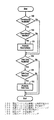
ここで図1を参照すると、システム10の一実施形態のブロック図が示されている。図示した実施形態において、システム10はホスト12と、DMAコントローラ14と、インターフェース回路16と、物理的インターフェース層(PHY)36とを含んでいる。DMAコントローラ14はホスト12とインターフェース回路16とに結合される。インターフェース回路16はさらに物理的インターフェース層36に結合されている。図示した実施形態において、ホスト12は、プロセッサ18A、18Bなどの1つ又は複数のプロセッサと、メモリ・コントローラ20A、20Bなどの1つ又は複数のメモリ・コントローラと、I/Oブリッジ(IOB)22と、I/Oメモリ(IOM)24と、I/Oキャッシュ(IOC)26と、レベル2(L2)キャッシュ28と、インターコネクト30とを含んでいる。プロセッサ18A、18B、メモリ・コントローラ20A、20B、IOB22、L2キャッシュ28はインターコネクト30に結合されている。IOB22はさらにIOC26とIOM24とに結合されている。DMAコントローラ14もIOB22とIOM24とに結合されている。図示した実施形態において、インターフェース回路16は周辺インターフェース・コントローラ32と、MAC34A、34Bなどの1つ又は複数のメディア・アクセス制御回路(MAC)とを含んでいる。MAC34A、34BはDMAコントローラ14と物理的インターフェース層36とに結合されている。周辺インターフェース・コントローラ32もI/Oブリッジ22とI/Oメモリ34とに結合され、(かつ、ひいては間接的にDMAコントローラ14に結合され)、かつ周辺インターフェース層36に結合されている。周辺インターフェース・コントローラ32及びMAC34A〜34Cは各々、構成レジスタ38A〜38Cを含んでいる。ある実施形態において、システム10のコンポーネントをチップ上のシステムとして単一の集積回路上に集積している。別の実施形態において、システム10を2つ以上の集積回路として実装している。
Referring now to FIG. 1, a block diagram of one embodiment of
ホスト12は1つ又は複数のアドレス空間を備えている。ホスト12内のアドレス空間の少なくとも一部はホスト12内の記憶領域にマッピングされている。すなわち、ホスト12はホストのアドレス空間内のアドレスにマッピングされたメモリ・システムを備えている。例えば、メモリ・コントローラ20A、20Bは各々、アドレス空間内にマッピングされた記憶領域を備えるメモリ(図示せず)に結合されている。ある場合は、アドレス空間全体が記憶領域にマッピングされている。別の場合は、アドレス空間の一部がメモリ・マップドI/Oでよい(例えば、周辺インターフェース・コントローラ32によって制御される周辺インターフェースが幾つかのメモリ・マップドI/Oを含んでいてもよい)。
The
DMAコントローラ14は、インターフェース回路16とホストのアドレス空間との間でDMA転送を行うように構成されている。特に、DMA転送は、アドレス空間がマッピングされた記憶領域とインターフェース回路16との間で行われる。加えて、ある実施形態において、DMAコントローラ14を、アドレス空間内の記憶領域のセット間でDMA転送を行うように構成している。すなわち、このようなDMA転送の転送元と転送先が記憶領域である。データ・ムーバの機能はこのようにDMAコントローラ14に組み込まれており、ある実施形態において、別のデータ・ムーバは必要がないこともある。メモリ間のDMA転送のためのプログラミング・モデルは、他のDMA転送(例えば以下に、より詳細に記載するDMA記述子)用のプログラミング・モデルと同様のものでもよい。メモリ間のDMA転送をコピーDMA転送と呼ぶこともある。
The
ある実施形態において、DMAコントローラ14を、DMAデータが転送される際にDMAデータに1つ又は複数のオペレーション(又は「関数」)を実行するように構成している。オペレーションはアドレス空間とインターフェース回路との間の転送に対して実行してもよく、ある実施形態において、コピーDMA転送に対して実行する。ある実施形態において、DMAコントローラ14が実行するオペレーションをプロセッサが実行する必要がないので、DMAコントローラ14によって実行されるオペレーションがプロセッサ18A、18Bにかかる処理負荷を軽減することがある。一実施形態において、DMAコントローラ14が実行するオペレーションの一部はパケット・データに対してなされるオペレーションである(例えば、暗号化/復号化、巡回冗長検査(CRC)の生成又はチェック、チェックサムの生成又はチェックなど)。オペレーションは、例えば安価ディスク冗長アレイ(RAID)処理に使用してもよい排他的OR(XOR)オペレーションをも含んでいる。
In some embodiments, the
一般に、DMA転送は、少なくとも1つの転送先がホストのアドレス空間内の記憶領域又はその他のアドレス(1つ又は複数)である、転送元から転送先へのデータ転送である。DMA転送は、転送されるデータがシステム内の1つ又は複数のプロセッサ(例えばプロセッサ18A、18B)を通過せずに達成される。DMAコントローラ14は転送元を読み出し、転送先を書き込むことによってDMA転送を達成できる。例えば、DMAコントローラ14が(図示した実施形態において、データを読み出すためにインターコネクト30上でコヒーレント読み出しトランザクションを実行するIOB22への)メモリ読み出し要求を生成し、読み出されたデータをDMAデータとしてインターフェース回路16に送信することによって、メモリからインターフェース回路16へのDMA転送を達成する。一実施形態において、DMAコントローラ14は、周辺インターフェース・コントローラ32を経たDMA転送のために、データをIOM24へ読み込む、読み込み要求を生成し、周辺インターフェース・コントローラ32は、IOM24からデータを読み出し、データを送信する。DMAコントローラ14がインターフェース回路16からデータを受け取り、DMAデータをメモリに転送する(図示した実施形態において、IOB22への)メモリ書き込み要求を生成することによって、インターフェース回路16からメモリへのDMA転送を達成する。一実施形態において、周辺インターフェース・コントローラ32がデータをIOM24に書き込み、DMAコントローラ14がデータをメモリに書き込ませる。したがって、DMAコントローラ14が周辺インターフェース・コントローラ32のためのDMAアシストを提供する。転送元の記憶領域へのメモリ読み出し要求、及び(メモリ読み出し要求によるDMAデータを含む)転送先の記憶領域へのメモリ書き込み要求を生成することによって、コピーDMA転送を達成することができる。
In general, DMA transfer is data transfer from a transfer source to a transfer destination, where at least one transfer destination is a storage area or other address (s) in the address space of the host. The DMA transfer is accomplished without the data being transferred passing through one or more processors (eg,
ホスト12は一般に、ホスト12のアドレス空間へとマッピングされたメモリとインターフェースするように構成された1つ又は複数のプロセッサとメモリ・コントローラを含んでいる。ホスト12は、ホスト12内でのプロセッサの性能を増強するためにL2キャッシュ28などの他の回路を場合により含んでいる。さらに、ホスト12は様々なI/O回路やDMAコントローラ14にインターフェースするための回路を含んでいる。ホスト12の1つの実装が図1に示されているが、他の実施形態は任意の構造を含み、かつDMAコントローラ14とインターフェース回路16へのインターフェースを含んでいる。
The
プロセッサ18A、18Bは、プロセッサ18A、18Bによって実装される命令セット・アーキテクチャ内で定義される命令を実行するための回路を備えている。様々な実施形態で任意の命令セット・アーキテクチャを実装している。例えば、PowerPC(商標)命令セット・アーキテクチャを実装している。他の例示的な命令セット・アーキテクチャはARM(商標)命令セット、MIPS(商標)命令セット、SPARC(商標)命令セット、(IA−32とも呼ばれる)x86命令セット、IA−64命令セットなどを含んでいる。
The
メモリ・コントローラ20A、20Bはメモリとインターフェースするように構成された回路を備えている。例えば、メモリ・コントローラ20A、20Bを、同期DRAM(SDRAM)、ダブル・データ・レート(DDR)SDRAM、DDR2 SDRAM、ラムバスDRAM(RDRAM)などのようなダイナミック・ランダム・アクセス・メモリ(DRAM)とインターフェースするように構成されている。メモリ・コントローラ20A、20Bは、これらがインターコネクト30から結合されるメモリ用の読み出しと書き込みトランザクションを受け取り、メモリに読み出し/書き込みオペレーションを実行する。読み出し、及び書き込みトランザクションは、DMAコントローラ14及び/又は周辺インターフェース・コントローラ32に代わってIOB22によって開始される読み出し及び書き込みトランザクションを含んでいる。加えて、読み出し及び書き込みトランザクションはプロセッサ18A、18B及び/又はL2キャッシュ28によって生成されるトランザクションを含んでいる。
The
L2キャッシュ28は、プロセッサ18A、18Bによる低潜在アクセス及び/又はインターコネクト30上の他のエージェントのために、メモリ・コントローラ20A、20Bが結合されているメモリ内の様々な記憶領域に対応するデータのコピーをキャッシュするように構成されたキャッシュ・メモリを備えている。L2キャッシュ28は任意の容量と構成(例えばダイレクト・マップ方式、群連想方式など)を備えている。
The
IOB22は、DMAコントローラ14と周辺インターフェース・コントローラ32の代わりにインターコネクト30上のトランザクションを通信するように構成された回路を備えている。インターコネクト30がキャッシュ・コヒーレンシをサポートしてもよく、IOB22がコヒーレンシに関与し、IOB22によって開始されるトランザクションのコヒーレンシを保証している。図示した実施形態において、IOB22は、IOB22によって開始された最近のトランザクションをキャッシュするためのIOC26を使用する。IOC26は様々な実施形態で任意の容量及び構成を有していてもよく、コヒーレントであっる。例えば、DMAコントローラ14と周辺インターフェース・コントローラ32によって生成される読み出し/書き込みに起因して部分的にしか更新されないデータ・ブロックをキャッシュするためにIOC26を使用することができる。場合によっては、IOC26を使用してインターコネクト30上の読み出し−修正−書き込みシーケンスを回避する。加えて、IOC26が読み出し/書き込みを完了するためにキャッシュ・ブロックの十分なオーナーシップを有している場合は、DMAコントローラ14又は周辺インターフェース・コントローラ32によって生成される読み出し/書き込み用のIOC26内のキャッシュ・ヒットのためのインターコネクト30上でのトランザクションを回避する。他の実施形態はIOC26を含んでいない。
The
IOM24を、周辺インターフェース・コントローラ32又はDMAコントローラ14とIOB22との間で転送されるデータ用のステージング・バッファとして使用している。したがって、IOB22とDMAコントローラ14/周辺インターフェース・コントローラ32との間のデータ・パスがIOM24を通っている。(読み出し/書き込み要求、要求と関連するホストのアドレス空間内のアドレスを含む)制御パスが直接、IOB22とDMAコントローラ14/周辺インターフェース・コントローラ32の間にある。他の実施形態において、IOM24が含まれない。
The
インターコネクト30は、プロセッサ18A、18B、メモリ・コントローラ20A、20B、L2キャッシュ28、IOB22の間で通信するための任意の通信媒体を含んでいる。例えば、インターコネクト30はコヒーレンシ・サポートを備えたバスである。あるいは、インターコネクト30は上記のエージェント間のポイント・ツー・ポイントインターコネクト、パケットベースのインターコネクト、又はその他のいずれかのインターコネクトでもよい。
The
インターフェース回路16は一般に、任意のインターフェース・プロトコルに従ってシステム10へのインターフェースで通信し、インターフェースで送信される通信を受信するためにシステム10内の他のコンポーネントと通信するか、又はインターフェースから受信された通信を供給するように構成された回路を備えている。インターフェース回路を、システム10内を転送元とする通信をインターフェース・プロトコルに変換し、システム10内で転送するためにインターフェースから受信された通信を変換するように構成している。例えば、インターフェース回路16は、周辺インターフェース・プロトコル(例えば周辺インターフェース・コントローラ32)に従って通信するように構成された回路を備えている。別の例として、インターフェース回路16は、ネットワーク・インターフェース・プロトコル(例えばMAC34A、34B)に従って通信するように構成された回路を備えている。
MAC34A、34Bは、ネットワーク・インターフェース用に定義されたメディア・アクセス・コントローラの機能を実装する回路を備えている。例えば、1つ又は複数のMAC34A、34Bがギガビット・イーサーネット標準を実装している。1つ又は複数のMAC34A、34Bが10ギガビット・イーサーネット・アタッチメント・ユニット・インターフェース(XAUI)標準を実装している。別の実施形態は、10メガビット又は100メガビット標準などの他のイーサーネット標準、又は他のいずれかのネットワーク標準を実装している。一実施形態において、6つのMACがあり、そのうちの4つがギガビット・イーサーネットMACであり、2つがXAUI MACである。他の実施形態は、それよりも多い、又はそれよりも少ないMAC、及び任意に組み合わせたタイプのMACを有している。
The
特に、イーサーネット標準を実装するMAC34A、34Bは、受信されたパケットからインターフレーム・ギャップ(IFG)、プリアンブル、フレーム開始デリミタ(SFD)を取り除いてもよく、DMAが記憶するよう残りのパケット・データをDMAコントローラ14に提供している。MAC34A〜34Dは、DMAから受信されたパケット用のIFG、プリアンブル、SFDを送信DMA転送として挿入し、パケットを送信用のPHY36に送信する。
In particular,
周辺インターフェース・コントローラ32は、周辺インターフェースを制御するように構成された回路を備えている。一実施形態において、周辺インターフェース・コントローラ32が周辺コンポーネント・インターコネクト(PCI)エクスプレス・インターフェースを制御している。別の実施形態は、PCIエクスプレス・インターフェースに加えて、又はその代替として他の周辺インターフェース(例えばPCI、PCI−X、ユニバーサル・シリアル・バス(USB)など)を実装している。
PHY36は一般に、インターフェース回路16に制御されてシステム10への外部インターフェースで物理的に通信するように構成された回路を備えている。特定の一実施形態において、PHY36はPCIエクスプレス・レーンとして、又はイーサーネット接続として使用するように構成されたシリアライザ/デシリアライザ(SERDES)回路のセットを備えている。PHY36はSERDES、及び同期先入れ先出し型(FIFO)バッファを経た送信用の8b/10bエンコード/デコードを実行する回路、及びさらにPICエクスプレス又はイーサーネット通信リンクとして使用するためにSERDESリンクを論理的に構成する回路を含んでいる。一実装形態では、PHYは、PCIエクスプレス・レーン又はイーサーネット接続として構成可能な24のSERDESを備えている。所望の任意の数のSERDESをPCIエクスプレスとして構成してもよく、所望の任意の数のSERDESをイーサーネット接続として構成している。
The
図示した実施形態において、周辺インターフェース・コントローラ32及びMAC34A、34B内の構成レジスタ38A〜38Cが示されている。各々の周辺インターフェース・コントローラ32及びMAC34A、34B内には1つ又は複数の構成レジスタがある。図1には示されていないが、システム10内には別の構成レジスタが存在している。構成レジスタを、周辺インターフェース・コントローラ32及びMAC34A、34Bの様々なプログラマブルに選択できるフィーチャを構成し、様々なフィーチャを有効化、無効化し、周辺インターフェース・コントローラ32及びMAC34A、34Bをオペレーション用に構成するなどに使用している。以下に記載の一実施形態において、構成レジスタを周辺インターフェース・コントローラ32及びMAC34A、34Bの実行時再構成のための制御記述子内で指定している。
In the illustrated embodiment,
様々な実施形態で、システム10が図1に示されたいずれかの要素(例えばプロセッサ、メモリ・コントローラ、キャッシュ、I/Oブリッジ、DMAコントローラ、及び/又はインターフェース回路など)のうちの1つ又は任意の数の要素を含んでいてもよいことに留意されたい。
In various embodiments, the
次に図2を参照すると、DMAコントローラ14の一実施形態のブロック図が示されている。図2の実施形態については、DMA転送を行わせる記述子ソフトウェア・モデルを記載する。ある実施形態において、記述子モデルに加えて、又はその代替として、レジスタを基本としたソフトウェア・モデルがサポートされている。レジスタを基本としたモデルでは、各々のDMA転送がDMAコントローラ14内にプログラムされ、DMAコントローラ14がDMA転送を行う。転送の完了時には、DMAコントローラ14はプロセッサ18A、18Bの1つに割り込むか、DMA転送の完了を判定するためにソフトウェアがポールできる(例えばDMAコントローラ14内部のレジスタ内の)ステータスを提供している。
Referring now to FIG. 2, a block diagram of one embodiment of the
記述子モデル内では、ソフトウェアがメモリ内の記述子データ構造を使用して多重DMA転送の実行を設定している。一般に、DMA記述子は、DMA転送を記述するデータ構造をメモリ内に備えている。例えば、DMA記述子内の情報は、DMA転送の転送元とターゲット、転送のサイズ、転送の様々な属性を特定する。場合によっては、DMA転送の転送元とターゲットは暗黙的でもよい。メモリ内の記述子データ構造内に(例えば「記述子リング」内に)複数の記述子が格納されてもよく、DMAコントローラ14にはデータ構造内の第1の記述子のアドレスがプログラムされている。DMAコントローラ14は記述子を読み出し、表示されたDMA転送を行う。ソフトウェアとハードウエアとの間の記述子のオーナーシップを制御するため、多様な制御機構を使用している。例えば、記述子は、記述子内に記述されたDMA転送の実行準備ができることをDMAコントローラ14に示す有効ビット、すなわちイネーブル・ビットを含んでいる。所与のDMA転送の終了時にDMAコントローラ14がプロセッサ18A、18Bに割り込むべきことを指示するために、記述子内の割り込みビットを使用してもよく、又は記述子が最後のDMA転送を記述しており、DMAコントローラ14が休止すべきであることを指示するために、転送終了ビットを使用することもできる。あるいは、DMAコントローラ14が処理のために幾つの記述子内を利用可能であるかを示すために、DMAコントローラ14が、ソフトウェアで増分できる記述子カウント・レジスタを実装している。DMAコントローラ14は記述子のプリフェッチが生成されたことを示すために、記述子カウント・レジスタを減分する。別の実施形態において、DMAコントローラ14は、記述子の消費(すなわち指定されたDMA転送の実行)を示すために記述子カウント・レジスタを減分する。さらに別の実施形態において、幾つの記述子が処理され、又はプリフェッチされたかを示すために、DMAコントローラ14は別個の記述子処理済みカウント・レジスタを使用する。
Within the descriptor model, software uses the descriptor data structure in memory to set up multiple DMA transfers. In general, a DMA descriptor has a data structure in a memory describing a DMA transfer. For example, the information in the DMA descriptor identifies the transfer source and target of the DMA transfer, the size of the transfer, and various attributes of the transfer. In some cases, the transfer source and target of the DMA transfer may be implicit. Multiple descriptors may be stored in a descriptor data structure in memory (eg, in a “descriptor ring”), and the
DMAコントローラ14は送信(Tx)DMA転送と受信(Rx)DMA転送とを実行できる。Tx DMA転送は転送元としてホスト12内にアドレス空間(例えばメモリ・コントローラ20A、20Bに結合されたメモリ内の記憶領域)を有している。Rx DMA転送はターゲットとしてホスト12内にアドレス空間を有している。Tx DMA転送はターゲットとしてインターフェース回路16を有し、又は(例えばコピーDMA転送用の)ターゲットとしてホスト12のアドレス空間内に別のアドレスを有している。ホスト・アドレス空間のターゲットを有するTx DMA転送は、転送元アドレスから読み出されたDMAデータをターゲット・アドレスに書き込むためにRx DMAデータ・パスを使用する。ループバック回路40がTx DMAデータ・パスとRx DMAデータ・パスとの間のリンクを提供している。すなわち、「ループバック回路」は、送信DMAデータ・パスからTx DMAデータを受信するために、かつ受信DMAデータ・パス上のRx DMAデータを供給するために結合されたDMAコントローラにローカルな回路を備えている。ループバック回路40によって受信DMAデータ・パス上に供給されるデータは、(例えばコピーDMA機能用の)送信DMAデータ・パスから受信されたデータである。ある実施形態において、ループバック回路40によって供給されるデータは、受信されたデータからループバック回路40によって変換されたデータである。ある実施形態において、ループバック回路40によって供給されるデータは、ループバック回路40によって受信され、ループバック回路40によってデータ(例えば、チェックサム、CRCデータなど)上で計算された結果によって増大されたデータである。あるいは、ループバック回路40によって供給されるデータは、ループバック回路40によって受信されたデータでもよく(又はデータが供給されなくてもよく)、その結果がDMA転送用の記述子内に格納されている。変換されたデータ、又は計算され、データと共に含まれ、又はDMA記述子に書き込まれる結果を、本明細書では総称して「結果」と呼んでもよい。
The
したがって、ある実施形態において、結果(例えば変換されたDMAデータ、又はデータから生成された結果)を生成するために、Tx DMAデータに1つ又は複数のオペレーション(又は「関数」)を実行するように、ループバック回路40を構成している。図2の実施形態において、ループバック回路40は、コピーFIFO42、オフロード・エンジン44、送信データ・パスに結合された排他的OR(XOR)回路46を含んでいる。コピーFIFO42は、Rx DMAデータ・パスでの送信用のTx DMAデータ・パスからの送信データを格納する。したがって、コピーFIFO42はコピーDMAオペレーションを実行する。オフロード・エンジン44を、DMAデータに様々なオペレーションを実行し、変換されたデータ、又はデータから分離された結果を生成するように構成している。様々な実施形態で、オフロード・エンジン44を、所望の任意のオペレーションセットを実行するように構成している。一実施形態において、オフロード・エンジン44を、パケット処理を支援するオペレーションを実行するように構成している。例えば、パケットの暗号化及び/又は認証を行う様々なネットワーク・セキュリティ・プロトコルが開発されている。認証は一般的には、パケットの一部又は全部にわたるハッシュの生成を含んでいる。したがって、オフロード・エンジン44を、DMA転送でパケット・データに暗号化/復号化、及び/又はハッシュ関数を実行するように構成する。加えて、オフロード・エンジン44を、チェックサムの生成/チェック、及び/又はCRCの生成/チェックを実行するように構成する。チェックサム及び/又はCRC保護は様々なパケット・プロトコルで使用されている。XOR回路46はビット単位のXOR DMAデータ(例えば複数の転送元からのDMAデータ)でよい。XOR回路46を、例えば安価ディスク冗長アレイ(RAID)の処理及び他のタイプの処理、又はXOR関数を使用する処理をサポートするために使用することができる。
Thus, in certain embodiments, one or more operations (or “functions”) are performed on Tx DMA data to generate results (eg, converted DMA data or results generated from data). In addition, a
ループバック回路40(及びより具体的には、ループバック・コンポーネント42、44及び46)は、DMAデータをループバック回路40に供給するDMA転送中にDMAデータ上で動作している。すなわち、ループバック回路40は、Tx DMA転送が残りのDMAデータを供給する間に、DMAデータへのオペレーションの実行を少なくとも開始している。一般に、結果をメモリに、より一般的にはホストのアドレス空間に(例えばDMAデータに添付された変換済みDMAデータとして、又はTx DMA転送用のDMA記述子内のフィールドなどの別個の結果記憶域に)書き込んでもよい。
The loopback circuit 40 (and more specifically, the
ループバック回路40はさらに、オフロード・エンジン44とXOR回路46(オフロード・エンジン44に結合されたオフロードFIFO48、及びXOR回路46に結合されたXOR FIFO 50)を含んでいる。FIFO48、50は、DMAデータが受信DMAデータ・パスで送信されるまで、オフロード・エンジン44とXOR回路46のそれぞれからのデータを一時的に格納する。図示した実施形態において、FIFO間を調停するためのアービタ52が備えられ、FIFO42、48、50に結合されている。アービタ52はループバックFIFO54にも結合され、これがターゲットに書き込まれるべきループバック回路40からのデータを一時的に格納する。
The
図示した実施形態において、DMAコントローラ14はTx DMAデータ・パス上のTx制御回路56と、Rx DMAデータ・パス上のRx制御回路58とを備えている。Tx制御回路56は送信DMA転送のためのホスト12からのデータをプリフェッチする。特に、Tx制御回路56はDMA記述子をプリフェッチしてもよく、DMAデータ用の転送元アドレスを決定するためにDMA記述子を処理する。Tx制御回路56は次いでDMAデータをプリフェッチする。Tx制御回路56のオペレーションを指すためにプリフェッチという用語を用いるが、プリフェッチは一般に、記述子やDMAデータをホストのアドレス空間から読み出すために生成されるオペレーションである。
In the illustrated embodiment, the
Tx制御回路56はDMAデータをターゲットに送信する。この実施形態において、ターゲットはインターフェース回路16又はループバック回路40のいずれか1つ(より具体的には、図示した実施形態において、コピーFIFO42、オフロード・エンジン44、XOR回路46の1つ)である。Tx制御回路56は(例えばターゲット識別子を送信することにより)送信済みデータのターゲットを特定する。あるいは、Tx制御回路56とインターフェース回路16との間、及びTx制御回路56とループバック・コンポーネント42、44、46との間に物理的に分離されたパスを設けている。Tx制御回路56は送信されるデータを一時的に格納するためバッファ62のセットを含んでいる。Tx制御回路56はさらに、様々な制御情報にデータを供給する。制御情報はDMA記述子からの情報を含んでいる。制御情報は、ループバック回路40用に、データをターゲット・アドレス空間に格納するためのバッファ・ポインタ(1つ又は複数)を含んでいる。制御情報はさらに、DMA記述子内に含まれ、かつインターフェース回路16又はループバック回路40によって使用される他のいずれかの制御情報を含んでいる。それらの例は、DMA記述子の説明に関連して以下に、より詳細に記載する。
The
Rx制御回路58はホスト12のアドレス空間に書き込まれるDMAデータを受信し、かつデータをメモリに格納する書き込みを行う。一実施形態において、ソフトウェアは、受信されたDMAデータを格納するためメモリ内にバッファを割り当てる。Rx制御回路58は、バッファ・ポインタ(バッファを識別するホストのアドレス空間のアドレス)を備えている。Rx制御回路58は、データを格納するための書き込み用のアドレスを生成するためにバッファ・ポインタを使用する。Rx制御回路58用のバッファ・ポインタをプリフェッチするため、Rxプリフェッチ・エンジン60を備えている。Rxプリフェッチ・エンジン60は、バッファ・ポインタをRx制御回路58に提供するために結合される。Rxプリフェッチ・エンジン60は、Rxプリフェッチ・エンジン60によって使用されるために、プリフェッチされたバッファ・ポインタを一時的に格納するためのバッファ64のセットを含んでいる。同様に、Rx制御回路58は、メモリに書き込まれる受信済みのDMAデータを一時的に格納するためのバッファ68のセットを含んでいる。
The
一実施形態において、Rx制御回路58を、受信されたDMAデータ用の記述子を生成するように構成する。すなわち、受信されたDMAデータ用のDMA記述子をソフトウェアに作成させるのではなく、ソフトウェアがDMAデータを格納するためのバッファを割り当て、バッファ・ポインタを提供している。Rx制御回路58は、割り当てられたバッファに受信されたDMAデータを格納し、DMA転送用の記述子を作成している。Rx制御回路58によって作成された記述子は、受信されたDMAデータを格納する1つ又は複数のバッファへの1つ又は複数のバッファ・ポインタ、及びDMA転送を記述する別の情報を含んでいる。受信DMA記述子の例示的実施形態が図12に示されており、以下に、より詳細に説明する。Rx制御回路58が、受信されたDMAデータ用の記述子を作成するので、記述子はソフトウェアによって作成された記述子よりも効果的である。例えば、ソフトウェアは最大の可能性があるDMA転送を受信することができるDMA記述子を作成する必要がある場合があり(又は、より大容量の転送用の複数の記述子が必要であり)、最大の可能性があるDMA転送を格納するための十分なバッファを割り当てる必要がある場合がある。一方、Rx制御回路58によって作成された記述子は、受信された実際の転送にとって十分大きい場合があり(かつ、受信されたデータを格納するのに十分なバッファを消費することがあるが)、必ずしもそれ以上大きい必要はない。
In one embodiment, the
図示した実施形態において、Rx制御回路58は、ループバックFIFO54に結合され、インターフェース回路16からのDMAデータをも受信するためのアービタ66からDMAデータを受信する。アービタ66は、データをRx制御回路58に転送するため、ループバックFIFO54と、インターフェース回路16から受信されたDMAデータとを調停する。
In the illustrated embodiment,
アービタ52、66は所望のいずれかの調停方式を実装している。例えば、優先度に基づく方式、ラウンドロビン方式、重み付きラウンドロビン方式、又はこれらの方式の組み合わせを用いる。ある実施形態において、調停方式がプログラマブルである。アービタ52によって実装される調停方式(1つ又は複数)は、アービタ66によって実装される方式(1つ又は複数)とは異なっている。
Tx制御回路56、Rxプリフェッチ・エンジン60、Rx制御回路58は、図示した実施形態において、IOM/IOBインターフェース・ユニット70に結合される。IOM/IOBインターフェース・ユニット56は、Tx制御回路56、Rxプリフェッチ・エンジン60、Rx制御回路58の代わりに、IOB22及びIOM24と通信する。IOM/IOBインターフェース・ユニット70は、Tx制御回路56、Rxプリフェッチ・エンジン60、Rx制御回路58からの読み出しと書き込みの要求を受け取り、これらの要求を満たすためにIOB22及びIOM24と通信する。
特に、IOM/IOBインターフェース・ユニット70は、記述子、及びTx制御回路56からのDMAデータの読み出し要求、及びRxプリフェッチ・エンジン60からのバッファ・ポインタを格納するメモリへの読み出し要求を受け取り、かつこの要求をIOB22に伝達する。IOB22はIOM24のどのエントリが要求されたデータ(例えば、ホストのアドレス空間又はIOC26からのデータの読み出し後、又は以前の要求からデータがIOB24内に既に存在することもある)を含むデータのキャッシュ・ラインを格納するか否かを示し、またIOM/IOBインターフェース・ユニット70はIOM24からデータを読み込み、そのデータをTx制御回路56又はRxプリフェッチ・エンジン60に供給する。IOM/IOBインターフェース・ユニット70はRx制御回路58からの書き込み要求も受け取ってもよく、IOM24に(IOB22によって書き込みデータ用に割り当てられたエントリで)書き込みデータを格納する。IOM24内にデータのキャッシュ・ラインが蓄積された後(又は、DMA転送の完了のいずれか先の方)、IOM/IOBインターフェース・ユニット70はその旨をIOB22に通知し、(バッファ・ポインタから書き込まれるバッファへと導き出された)キャッシュ・ラインが書き込まれるアドレスを提供する。
In particular, the IOM /
一実施形態において、DMAコントローラ14はDMA転送を送信し、DMA転送を受信するための様々なチャネルをサポートしている。様々な実施形態で、任意の数のチャネルがサポートされている。例えば、一実装形態では、20の送信DMAチャネルを備え、64の受信DMAチャネルを備えている。各チャネルは転送元から転送先までの独立した論理データ・パスでよい。チャネルは、ソフトウェアにより所望通りに割り当てられる。
In one embodiment,
より具体的には、各送信チャネルをインターフェース回路16の1つ、又はループバック・コンポーネント回路42、44、又は46の1つに割り当てる。全ての送信チャネルが使用される必要はない(すなわち、送信チャネルの一部は無効化されてもよい)。Tx制御回路56は、チャネルごとにDMA記述子とDMAデータをプリフェッチする。すなわち、Tx制御回路56は、処理に利用できるDMA記述子を有する各チャネルごとに独立してプリフェッチを生成している。Tx制御回路56は、生成されたプリフェッチからIOM/IOBインターフェース・ユニット70への読み出し要求を送信するためのプリフェッチを選択している。
More specifically, each transmission channel is assigned to one of the
インターフェース回路16の1つに各受信チャネルを割り当てる。必ずしも全ての受信チャネルが使用される必要はない(すなわち、受信チャネルの一部は無効化されてもよい)。Rx制御回路58は、受信されたデータと共にチャネル番号を受信する。ループバック回路40はDMA記述子からDMA用のバッファ・ポインタを供給してもよく、Rx制御回路58は、DMAデータをホストのアドレス空間に書き込むためにバッファ・ポインタを使用する。割り当てられたチャネルでインターフェース回路16がプログラム可能であってもよく、チャネルを決定するためにパケット・フィルタリングを使用してもよい。インターフェース回路16はチャネル番号にDMAデータを供給してもよく、Rx制御回路58は、DMAデータをホストのアドレス空間に書き込むためのチャネル用にRxプリフェッチ・エンジン60から提供されたバッファ・ポインタを使用してもよい。
Each reception channel is assigned to one of the
DMAコントローラ14は、図2に示されているような様々な構成レジスタ38D〜38Hを含んでいる。構成レジスタ38A〜38Hは、DMAコントローラ14の様々なプログラム可能なフィーチャを有効化/無効化するために、かつ/又は前述のように、プログラム可能フィーチャを構成するためにプログラム可能である。例えば、Tx制御回路56内の構成レジスタ38Dは、各チャネルごとの記述子リングのアドレス、及び利用可能な記述子の数を示す記述子カウントを含んでいる。構成レジスタ38Dはさらに、インターフェース回路16への送信チャネルの割り当て、及びコンポーネント・ループバック機能を含んでいる。チャネルごとの様々な他の構成、及びチャネルに関連しない構成が構成レジスタ38Dに格納されている。同様に、構成レジスタ38Eは、各インターフェース回路16、バッファ・リング・カウントなどのためのバッファ・ポインタ・リングのアドレス、及びチャネルに関連しない様々な構成を格納する。構成レジスタ38Fは様々な受信DMA構成を格納する。構成レジスタ38Gは、ループバック回路40用の構成全体、及び所望の各コンポーネント回路用の構成を格納する。構成レジスタ38Gはアービタ52用の構成(例えば、調停方式の選択、選択された調停方式の構成のプログラミング)をも格納する。構成レジスタ38Hはアービタ66用の調停の構成を格納する。
The
Tx制御回路56は記述子とDMAデータを取得するためにプリフェッチを実装するが、他の実施形態はプリフェッチを実装しない場合もあることに留意されたい。したがって、一般に、送信DMA転送(及びループバック回路40へのDMA転送)を行うように構成されたTxエンジン56、又はTx制御回路56がある。
Note that although the
この説明はDMA転送のためのバッファとバッファ・ポインタに言及したものであることに留意されたい。(62、64、68などのハードウエア記憶バッファではなく)バッファ・ポインタによって指されるバッファは連続記憶領域を備えている。(送信のために、又はDMAデータを受信するための領域として)DMAデータを格納するためにソフトウェアが記憶領域を割り当てる。バッファ・ポインタは、ホストのアドレス空間内の記憶領域のアドレスを備えている。例えば、バッファ・ポインタは記憶領域のベース、又は記憶領域の境界を指している。 Note that this description refers to buffers and buffer pointers for DMA transfers. The buffer pointed to by the buffer pointer (not the hardware storage buffer such as 62, 64, 68, etc.) has a continuous storage area. Software allocates a storage area to store DMA data (for transmission or as an area for receiving DMA data). The buffer pointer comprises the address of a storage area in the host address space. For example, the buffer pointer points to the base of the storage area or the boundary of the storage area.
次に図3を参照すると、オフロード・エンジン44の一実施形態のブロック図が示されている。図示した実施形態において、オフロード・エンジン44は入力バッファ80と、出力バッファ82と、セキュリティ回路のセット84A〜84Dと、CRC生成器86と、チェックサム生成器88とを含んでいる。入力バッファ80はTx制御回路56と、セキュリティ回路84A〜84Dと、CRC生成器86と、チェックサム生成器88とに結合される。出力バッファ82はセキュリティ回路84A〜84Dと、CRC生成器86と、チェックサム生成器88とに結合される。出力バッファ82はオフロードFIFO48にも結合される。一実施形態のセキュリティ回路84Aが図3に、より詳細に示されており、セキュリティ回路84B〜84Dは同様のものでよい。セキュリティ回路84Aはハッシュ回路90と暗号回路92とを含んでいる。ハッシュ回路90及び暗号回路92は双方とも入力バッファ80と出力バッファ82とに結合される。加えて、ハッシュ回路90の出力は、入力として暗号回路92に結合されており、暗号回路92の出力は、入力として「バタフライ」構造でハッシュ回路90に結合される。
Referring now to FIG. 3, a block diagram of one embodiment of the
セキュリティ回路84A〜84Dは、パケット処理のセキュリティ機能をオフロードするために様々なオペレーションを行うように構成される。特に、セキュリティ回路84A〜84Dは、暗号化/復号化(集合的に暗号化、又は暗号機能と呼ばれる)、及び様々なセキュア・パケット仕様(例えばセキュア・インターネット・プロトコル(IPSec)、又はセキュア・ソケット・レイヤー(SSL))に含まれるハッシュ関数を実行するように構成される。
一般的には、セキュア・パケット・プロトコルを使用する通信には、エンドポイントがそれが使用することができるプロトコルと通信する交渉セッション、エンドポイントがサポートするセキュリティ方式、暗号化とハッシュのタイプ、キーの交換又は認証などが含まれる。その場合、合意に基づくプロトコル、暗号化などを使用したバルク転送段階がある。バルク転送中、(例えばインターフェース回路16の1つから受信DMAパスを経て)パケットがホスト12内に受信される。ソフトウェアは、キー、暗号化アルゴリズムなどを得るためにメモリ内のデータ構造を調査し、パケットを復号化、及び/又は認証するためにオフロード・エンジン44を介してDMA転送を準備する。同様に、ソフトウェアはセキュア送信のためのパケットを準備し、パケットを暗号化及び/又は認証するためにオフロード・エンジン44を介してDMA転送を使用する。
In general, for communication using secure packet protocols, the endpoint communicates with the protocol that it can use, the security method supported by the endpoint, the type of encryption and hash, the key Exchange or authentication. In that case, there is a bulk transfer stage using agreement-based protocols, encryption, etc. During a bulk transfer, a packet is received in the host 12 (eg, via a receive DMA path from one of the interface circuits 16). The software examines the data structure in the memory to obtain keys, encryption algorithms, etc., and prepares DMA transfers via the
ハッシュ回路90は、パケットの認証に使用できる様々なハッシュ関数を実装している。一般的には、ハッシュはパケットの少なくとも一部にわたって計算され、ハッシュ結果がパケット内に含められる。パケットが転送先で受信されると、パケット内のいずれかのフィールドが変更されたか否かを検知するために(ひいてはパケットがその転送元からの転送で修正されたか否かを検知するために)、ハッシュがチェックされる。一実施形態において、ハッシュ回路90内で以下のハッシュ関数がサポートされている:メッセージ・ダイジェスト5(MD−5)/セキュア・ハッシュ・アルゴリズム−1(SHA−1)、及びハッシュ・メッセージ認証コード(HMAC)。他の実施形態はSHA−2を実装している。他の実施形態は、上記の関数、及び他の関数のサブセット又はスーパーセットを含む他のいずれかのハッシュ関数のセットを実装している。
The
暗号回路92を、暗号化関数を実行するように構成する。セキュア・パケット仕様に応じて、場合によってはハッシュ・データを含むパケットの少なくとも一部に暗号化関数が適用される。暗号化関数のいずれものセットは、様々な実施形態でサポートされている。例えば、一実施形態において、以下の暗号化/復号化アルゴリズムが暗号回路92に実装さる。すなわち、データ暗号化標準(DES)、トリプル・データ暗号化標準(3DES)、先進データ暗号化標準(AES)、Kasumi、主張されているロンのコード4(ARC4)、及び/又はロンのコード4(RC4)である。
The
ある場合には、認証及び暗号化の双方の関数が使用される場合は、送信用にパケットが準備されるときに最初に暗号化が行われ、次いで暗号化されたデータ(例えばIPSec)に認証ハッシュが実行される。別の場合は、認証ハッシュが最初に実行され、二番目に(ハッシュ・データを含む)パケットの暗号化が実行される(例えばSSL)。いずれの場合も、認証ハッシュと復号化は受信されたパケットでは逆の順序で行われる。 In some cases, if both authentication and encryption functions are used, encryption is performed first when the packet is prepared for transmission, and then authenticated to the encrypted data (eg IPSec) A hash is performed. In another case, an authentication hash is performed first and a second (including hash data) packet encryption is performed (eg, SSL). In either case, the authentication hash and decryption are performed in the reverse order on the received packet.
セキュリティ回路84A〜84Dは、回路90と92との間のバタフライ接続を介して、単一のDMA転送でのどの順序でのデータの暗号化及びハッシュもサポートできる。すなわち、暗号化が最初に実行される場合は、暗号化(又は復号化される)データでハッシュ関数を計算するために、セキュリティ回路84Aに供給されるデータが暗号回路92に送られ、暗号回路92の出力がハッシュ回路90の入力に送られる。最初にハッシュが実行される場合は、セキュリティ回路84Aに供給されるデータがハッシュ回路90に送られ、ハッシュ回路90の出力が暗号回路92の入力に送られる。セキュリティ回路84A〜84Dは、所定のDMA転送でハッシュ関数のみ又は暗号化関数のみの実行をもサポートする。セキュリティ回路84A〜84Dに向けられるDMA転送用のDMA記述子からの制御情報が、セキュリティ回路84A〜84Dを経たデータの伝送を制御する。
図示した実施形態は、4つのセキュリティ回路84A〜84Dを示している。他の実施形態は、1つのセキュリティ回路を含む任意の数のセキュリティ回路を含んでもよい。一実施形態において、セキュリティ回路84A〜84Dは、システム10で使用されるシステム・クロックの周波数の2倍の周波数でクロックされ、システムのクロック周期ごとに、(1つはシステム周期クロックの最初の半期で実行され、もう1つはシステムのクロック周期の第2の半期で実行される)2つのオペレーションを受け取る。したがって、セキュリティ機能を実行するために、ソフトウェアによって選択される8つのセキュリティ論理回路がある。
The illustrated embodiment shows four
CRC生成器86を、CRC生成を指定するDMA転送で供給されるデータ上にCRCデータを生成するように構成する。CRC生成を、受信されたパケットからのCRCデータをチェックするために使用する。例えば、CRC生成器86内で生成されたデータが、受信されたパケット内の対応するCRCデータと比較される。あるいは、受信されたパケット内のCRCデータを、CRC生成器86を経たDMA転送に含めてもよく、受信されたパケット内のエラーを検知するために、その結果を所定値と比較してチェックする。ある実施形態において、2つ以上のCRC生成器86がある。さらに、オフロード・エンジン44内に物理的に備えられるものよりも多くの論理的CRC生成器を備えるため、セキュリティ回路84A〜84Dと同様に、CRC生成器86(1つ又は複数)がシステムのクロック周期数の2倍の周波数でクロックされる。特定の一実施形態において、等しい数の論理ユニット(8)をセキュリティ回路84A〜84Dに備えるため、システムのクロック周波数の2倍の周波数でクロックされる4つのCRC生成器86がある。
The
チェックサム生成器88を、チェックサム生成を指定するDMA転送で供給されるデータ上にチェックサムを生成するように構成する。チェックサム生成を、受信されたパケットからのチェックサム・データをチェックするために使用する。例えば、チェックサム生成器88内で生成されたデータが、受信されたパケット内の対応するチェックサムと比較される。あるいは、受信されたパケット内のチェックサム・データを、チェックサム生成器88を経たDMA転送に含めてもよく、受信されたパケット内のエラーを検知するために、その結果を所定値と比較してチェックする。ある実施形態において、2つ以上のチェックサム生成器88がある。
入力バッファ80は、ターゲット回路84A〜84D、86、又は88がデータに対してオペレーションを行うまで、Tx制御回路56によって供給されるデータを一時的に格納する。ターゲット回路84A〜84D、86、88は、オフロードFIFO48に書き込まれる出力データを出力バッファ82に出力する。別の実施形態において、入力バッファ80、及び/又は出力バッファ82を含めなくてもよい。
図4は、システム10の一実施形態で実装されてもよいDMAのモデルの一実施形態を示すブロック図である。前述のように、DMA転送は、転送元のアドレス空間又はインターフェース(ブロック100)から転送先のアドレス空間又はインターフェース(ブロック102)へと行われる。DMA転送は図4のブロック104で表わされる。場合によって、DMA転送は、結果を生成するためにDMAデータに対する1つ又は複数のオペレーション、又は関数の実行(ブロック106)を含む。結果はDMAブロック104に戻され、ターゲットのアドレス空間に供給される。ある場合は、結果を、ターゲットのアドレス空間に書き込むことができるDMAデータに変換する。別の場合は、結果をDMAデータから分離し、DMAデータを増大して(例えばDMAデータの終端に添付)、又は別個の位置内に(例えば、DMA転送用のDMA記述子内に)格納する。
FIG. 4 is a block diagram illustrating one embodiment of a model of DMA that may be implemented in one embodiment of
図4は、ある場合は単一のDMA転送を示す。別の場合は、図4のモデルを完成させるために複数のDMA転送を使用する。例えば、関数106をループバック回路40(又は、図2の実施形態の場合はそのコンポーネント)によって実行する。したがって、図示した実施形態において、インターフェース回路16をターゲットとするDMA転送で関数を実行したい場合は、2つのDMA転送を行う。第1のDMA転送は、転送元のアドレス空間からターゲットのアドレス空間に対して行われ、実行される所望の関数を指定する。引き続いて、転送元として第1のDMA転送のターゲットのアドレス空間、及びターゲットとして所望のインターフェース回路を使用して第2のDMA転送を行う。
FIG. 4 shows a single DMA transfer in some cases. In other cases, multiple DMA transfers are used to complete the model of FIG. For example, function 106 is performed by loopback circuit 40 (or its components in the case of the embodiment of FIG. 2). Therefore, in the illustrated embodiment, when a function is to be executed by DMA transfer targeting the
例えば、MAC34A、34Bを介して転送用のソフトウェアを使用してパケットを準備してもよく、パケットをホスト12内のメモリに格納する。暗号化及び/又はハッシュを使用したセキュア転送が望ましいことがあり、したがって、ソフトウェアがホスト12内の第1の記憶領域から第2の記憶領域への第1のDMA転送を構築してもよく、第1のDMA転送がオフロード・エンジン44内で暗号化及び/又はハッシュを指定している。ソフトウェアはさらに、第2の記憶領域からターゲットMAC34A、34Bへの第2のDMA転送を準備する。同様に、パケットは、DMAとしてホスト12内のメモリ内に受信されて、パケットのハッシュ及び/又は復号化をチェックするため、ソフトウェアがオフロード・エンジン44を介したDMA転送を行う。
For example, a packet may be prepared by using software for transfer via the
別の実施形態は、データがインターフェース回路16に送信される際に、関数の適用を許容している。例えば一実施形態において、TCPパケットのTCPヘッダ内に含まれるチェックサムを生成するため、IOB22内で部分的チェックサムの生成がサポートされる。このようなパケット向けにDMA転送が指定されると、IOB22がこのパケット・データをIOM24に累積し、各キャッシュ・ラインごとに部分的チェックサムを生成す。IOB22からの各キャッシュ・ライン及び、部分的チェックサムが計算されなかったデータに、部分的チェックサムを使用してDMAコントローラ14内で最終チェックサムが生成されてもよく、DMAコントローラ14が、計算されたチェックサムをTCPヘッダに挿入する。別の実施形態は、関数が実行され、データが送信される単一のDMA転送の一部として、ループバック回路40の出力が直接インターフェース回路16に送られることを許容している。さらに、別の実施形態は、受信DMA転送中に受信されたDMAデータ上で関数を実行するため、Rx DMAデータ・パスからのデータがループバック回路40に入力されることを許容している。
Another embodiment allows the application of functions as data is transmitted to the
次に図5を参照すると、記述子のデータ構造とバッファ・ポインタのデータ構造を格納する記憶領域110のブロック図が示されている。図5の実施形態において、記述子のデータ構造は記述子リングのセット112A〜112Nを含んでいる。DMAコントローラ14によってサポートされる各DMAチャネル(例えば図5のチャネル0からチャネルN)ごとに1つの記述子がある。すなわち、DMAチャネルと記述子リングとの間には1対1の対応関係があり、所定のDMAチャネル用のDMA転送は、チャネルに割り当てられた記述子リング112A〜112N内に対応する記述子を有している。加えて、図5に示された実施形態において、バッファ・ポインタのデータ構造はバッファ・ポインタ・リングのセット114A〜114Mを含んでいる。インターフェース回路16ごとに(例えば図5では、インターフェース回路0からM、ただしM+1はインターフェース回路16の数でよい)、バッファ・ポインタ・リングがある。すなわち、インターフェース回路と記述子リングとの間には1対1の対応関係があり、そのインターフェースで受信されるDMA用に使用されるバッファ・ポインタが、そのインターフェース回路に割り当てられたバッファ・ポインタ・リング114Aから114Mから取り出される。
Referring now to FIG. 5, a block diagram of a
各記述子リング112A〜112Nは対応するDMAチャネル用の記述子のセットを備えている。送信DMAチャネル用には、記述子はリング内の最初の記述子から最後の記述子までリング内に含まれる順序で処理され、次いで最後の記述子が処理された後、リング内の最初の記述子に折り返される。したがって、任意の時点で、リング内のどのリングも、次に処理されるべき「現在の記述子」であると見られる。前述のように、ソフトウェアが、多様な方式でのDMAチャネルでの処理に利用できる記述子の数を制御している。したがって、(対応する記述子リング内に)所定の送信DMAチャネルで利用できる記述子があれば、DMAコントローラ14は(他のDMAチャネルを有するリソースと調停して)指定のDMA転送を実行する。本実施形態の受信DMA転送の場合は、DMA転送がそのチャネルで受信されると、対応する記述子リング内の記述子が消費される。DMAコントローラ14は、受信されたDMAデータを格納するために使用されるバッファ・ポインタ(1つ又は複数)で現在の記述子、及び転送ステータス情報などのDMA転送に関連する他の情報を書き込んでもよい。
Each
別の実施形態は他のデータ構造(例えば記述子のリンクされたリスト)を使用する。各記述子リング112A〜112Nのベース・アドレスが(例えば、チャネルが送信チャネルであるか受信チャネルであるかに応じて、構成レジスタ38D又は38F内にプログラムされて)DMAコントローラ14に提供される。記述子リング112A〜112Nの他の属性(例えば範囲)もプログラムされる。ある実施形態において、所定のリング内の記述子は固定サイズのものでよいので、所定の記述子はリングのベース・アドレスから固定的にオフセットされる。別の実施形態において、記述子は可変サイズのものでよい。さらに別の実施形態において、記述子は、構成レジスタ38D又は38F内のプログラム可能な属性に応じて、固定サイズのものでも可変サイズのものでもよい。属性はチャネルごとにプログラム可能なものでもよく、又はチャネル全体としてプログラムされる。
Another embodiment uses other data structures (eg, a linked list of descriptors). The base address of each
各バッファ・ポインタ・リング114A〜114Mは、対応するインターフェースからのRx DMA転送からのDMAデータを格納するために使用されるソフトウェアによって割り当てられたメモリ内のバッファを指すバッファ・ポインタを備えている。記述子リング112A〜112Nと同様に、ソフトウェアは、バッファ・ポインタ・リング114A〜114M内のバッファ・ポインタを任意の所望の方式でDMAコントローラ14に利用できるようにしている。各インターフェース用のバッファ・ポインタ・リングのベース・アドレスが、(例えば、図2の実施形態のRxプリフェッチ・エンジン60内の構成レジスタ38E内で)DMAコントローラ14内にプログラムされてもよく、所定の任意の時点でバッファ・ポインタ・リング内のバッファ・ポインタの1つが、対応するインターフェース用に次に消費されるバッファ・ポインタである。
Each
DMAチャネルではなく、インターフェース回路に関連するバッファ・ポインタ・リング114A〜114Mを備えることによって、ある実施形態において、ソフトウェアはより多数のDMAチャネルではなくより少数のインターフェース回路にバッファを割り当てられる。ある場合は、このメモリの割り当ての方が効率的である。そのトラヒックがどのチャネルで受信されるかをソフトウェアが前もって知る必要なく、より多くのトラヒックを扱うインターフェース回路により多くのバッファを割り当てる。DMAデータが所定のインターフェースから受信されると、そのインターフェースに割り当てられたバッファ内にデータが格納され、DMAデータが受信されるチャネル用の記述子にバッファ・ポインタが書き込まれる。どの受信DMAチャネルがDMA転送に関連しているかに応じて、記述子は記述子リング112A〜112Nの1つにある。 By providing buffer pointer rings 114A-114M associated with interface circuits rather than DMA channels, in certain embodiments, software can allocate buffers to fewer interface circuits rather than more DMA channels. In some cases, this memory allocation is more efficient. More buffers are allocated to interface circuits that handle more traffic without the software needing to know in advance which channel that traffic is received on. When DMA data is received from a given interface, the data is stored in a buffer assigned to that interface, and a buffer pointer is written to the descriptor for the channel on which the DMA data is received. Depending on which receive DMA channel is associated with the DMA transfer, the descriptor is in one of the descriptor rings 112A-112N.
バッファ・ポインタ・リング114A〜114Mは、バッファ・ポインタごとのサイズ・フィールド(図5のSz)をも含んでいる。サイズ・フィールドが、対応するバッファ・ポインタによって指されるバッファのサイズを示している。したがって、例えば利用可能なメモリ量、所定のインターフェース上の予測されるDMA転送のサイズなどに基づいて、ソフトウェアが異なるサイズのバッファを割り当てる。 The buffer pointer rings 114A-114M also include a size field (Sz in FIG. 5) for each buffer pointer. The size field indicates the size of the buffer pointed to by the corresponding buffer pointer. Thus, for example, the software allocates buffers of different sizes based on the amount of available memory, the size of the expected DMA transfer on a given interface, and the like.
次に図6を参照すると、所定のインターフェース回路についてRxプリフェッチ・エンジン60の一実施形態のオペレーションを示すフローチャートが示されている。Rxプリフェッチ・エンジン60は、並行して、かつ独立して動作する各インターフェース回路ごとに図6に示されたオペレーションを実行する回路を含んでいる。容易に理解できるように、図6には特定の順序でブロックが示されているが、ブロックは図6に示されたオペレーションを実行する組み合わせの論理回路で並行して実行されてもよい。ある実施形態において、1つ又は複数のブロック又はフローチャート全体が複数のクロック周期にわたってパイプライン接続される。
Referring now to FIG. 6, a flowchart illustrating the operation of one embodiment of the
Rxプリフェッチ・エンジン60は、(インターフェース回路に対応するバッファ・ポインタ・リング114A〜114M内の)インターフェース回路用のバッファ・ポインタを利用可能であるか否か(決定ブロック120)、かつ、インターフェース回路にバッファ・ポインタが必要であるか否か(決定ブロック122)を判定する。少なくとも1つのバッファ・ポインタが利用可能であり、必要である場合は(決定ブロック120、122の「yes」区間)、Rxプリフェッチ・エンジン60はホスト12内のメモリ内のバッファ・ポインタ・リング114A〜114Mからバッファ・ポインタ(1つ又は複数)を読み出すプリフェッチ要求を生成する(ブロック124)。
バッファ・ポインタは一般に、Rxプリフェッチ・エンジン60によって未だプリフェッチされていない対応するバッファ・ポインタ・リング114A〜114M内にバッファ・ポインタがあれば「利用可能」である。ソフトウェアによってバッファ・ポインタがバッファ・ポインタ・リング114A〜114M内に挿入されてもよく、ソフトウェアは、前述の方式のいずれかで(例えばバッファ・ポインタ・リングのエントリ内の有効ビットを使用し、前述のDMA記述子カウントと同様のバッファ・ポインタ・リングのカウントを増分して)バッファ・ポインタが利用可能であることを指示している。同様に、バッファ・ポインタは多様な方式で「必要である」と見られる。例えば、受信DMAチャネルが有効化され、そのチャネル用にプリフェッチされたバッファ・ポインタがない場合は、バッファ・ポインタは「必要である」可能性がある。ある実施形態において、プリフェッチされるべきいくつかのバッファ・ポインタを示し、又はプリフェッチされるべき最小数と最大数のバッファ・ポインタを示すようにRxプリフェッチ・エンジン60がプログラムされる。Rxプリフェッチ・エンジン60は、プログラムされた数のバッファ・ポインタのプリフェッチを試みるために、バッファ・ポインタのためのプリフェッチ要求を生成する。
A buffer pointer is generally “available” if there is a buffer pointer in the corresponding
前述のように、図6のオペレーションが、有効化された各々のインターフェース回路ごとに並行して行われる。2つ以上のプリフェッチ要求が同時に生成される場合は、Rxプリフェッチ・エンジン60はプリフェッチ要求の中から選択するための回路も含む。例えば、一実施形態において、Rxプリフェッチ・エンジン60はプリフェッチ要求の中から固定優先度方式を実装する。別の実施形態において、Rxプリフェッチ・エンジン60は、最少数のバッファ・ポインタが現在選択され、準備ができるインターフェース回路に対応するプリフェッチ要求を選択する。別の実施例として、Rxプリフェッチ・エンジン60は、現在プリフェッチされるバッファ・ポインタと、そのインターフェース回路用の所望のバッファ・ポインタ数との最大の差をどのインターフェース回路が有しているか否かに基づいて要求に重み付けする。さらにラウンドロビン又は優先度に基づく選択機構も利用してもよく、必要ならば、これらの機構はインターフェース回路間のプログラム可能な重みを含む。ポインタが各インターフェース回路ごとにプリフェッチされることを保証するため、インターフェースごとのタイムアウトなどの飢餓状態防止機構をも使用できる。
As described above, the operation of FIG. 6 is performed in parallel for each enabled interface circuit. If more than one prefetch request is generated simultaneously, the
プリフェッチされたバッファ・ポインタが読み出されるべきIOM24内で利用可能である場合は、IOM/IOBインターフェース回路70によってその旨がRxプリフェッチ・エンジン60に通知される。ある実施形態において、Rxプリフェッチ・エンジン60はIOM24からポインタの一部又は全部を読み出し、プリフェッチされたバッファ・ポインタを必要に応じてRx制御回路58に供給する。
If the prefetched buffer pointer is available in the
次に図7を参照すると、Rx制御回路58の一実施形態の、データの受信に応答したオペレーションを示したフローチャートが示されている。データはループバック回路40、又はインターフェース回路16のどちらから受信される。図7では理解し易いように、ブロックが特定の順序で示されているが、ブロックは図7に示されたオペレーションを実行する組み合わせの論理回路で並行して実行される。ある実施形態において、1つ又は複数のブロック又はフローチャート全体が複数のクロック周期にわたってパイプライン接続される。
Referring now to FIG. 7, a flowchart illustrating the operation of one embodiment of the
Rx制御回路58は、DMAデータを受信するためにバッファが既に使用中であるか否かを判定する(決定ブロック130)。バッファがDMAデータを格納するために既に選択されており、未だフル状態になっていない場合は、バッファは使用中である。Rx制御回路58を、ループバック回路40用の各Rxチャネル及び1つ又は複数のバッファ・ポインタ用の能動バッファを保持するように構成する。あるいは、ループバック回路40はバッファ・ポインタに各データ転送を供給してもよく、Rx制御回路58がループバック回路40用にポインタを保持しない。バッファが使用中ではない場合は(決定ブロック130、「no」区間)、Rx制御回路48は、読み出されるバッファを識別するために次のバッファ・ポインタを選択する。ループバック回路40からのDMA転送用には、ループバック回路40によって次のバッファ・ポインタが提供される。インターフェース回路16からのDMA転送用には、Rxプリフェッチ・エンジン60から次のバッファ・ポインタが提供され、Rx制御回路58はRxプリフェッチ・エンジン60にポインタの消費を指示している。
The
いずれの場合も、Rx制御回路58は受信されたデータをバッファに書き込んでもよい(ブロック134)。すなわち、Rx制御回路58はIOM/IOBインターフェース回路70に対してDMAデータをメモリに書き込むための書き込み要求を生成している。Rx制御回路58は、少なくともインターフェース回路16から受信されたデータについて、バッファがフル状態である場合にその旨を判定するため、バッファに書き込まれたバイト数を監視している。ある実施形態において、ループバック回路40によってバッファのサイズが提供され、Rx制御回路58がループバック転送についてもバッファのフル状態を監視している。バッファがフル状態である場合、又は転送元(ループバック回路40、又はインターフェース回路16)によってデータ転送がDMA転送の終了であるものと示された場合は(決定ブロック136、「yes」区間)、Rx制御回路58はDMA転送用の記述子にバッファ・ポインタを書き込む(ブロック138)。ループバック転送の場合は、バッファ・ポインタが転送元のDMA記述子からの転送先バッファ・ポインタであるので、受信されたデータ用のDMA記述子はなくてもよく、このような転送にはブロック138は実行されない。データ転送がDMA転送の終了であることが示された場合は(決定ブロック140、「yes」区間)、Rx制御回路58は、転送処理の様々な終了を実行する(ブロック142)。例えば、インターフェース回路16からのDMA転送の場合、Rx制御回路58はDMA転送用の様々なステータスを生成し、転送用のDMA記述子のヘッダを生成し、かつデータが受信されたRx DMAチャネルに対応する記述子リング112A〜112NにDMA記述子を書き込む。加えて、Rx制御回路58は、IOM/IOB回路70に転送終了を信号通知する。転送終了の信号通知はIOM/IOB回路70に対して、そのチャネルにはそれ以上のデータは供給されないことを通知する。未完了のキャッシュ・ラインがDMAによって更新されると、IOM/IOB回路70は更新されたデータがメモリに(例えば、ある実施形態において、インターコネクト30での読み出し−修正−書き込みを避けるため、IOC26内に)格納される。
In either case,
次に図8を参照すると、所定のTx DMAチャネル用のTx制御回路56の一実施形態のオペレーションを示すフローチャートが示されている。Tx制御回路56は、並行して、かつ独立して動作する各Tx DMAチャネルごとに図8に示されたオペレーションを実行する回路を含んでいる。容易に理解できるように、図8には特定の順序でブロックが示されているが、ブロックは図8に示されたオペレーションを実行する組み合わせの論理回路で並行して実行されてもよい。ある実施形態において、1つ又は複数のブロック又はフローチャート全体が複数のクロック周期にわたってパイプライン接続される。
Referring now to FIG. 8, a flowchart illustrating the operation of one embodiment of the
Tx制御回路56は、(チャネルに対応する記述子リング112A〜112N内の)プリフェッチ用のチャネルを利用可能であるか否か(決定ブロック150)、かつ、チャネルに記述子が必要であるか否か(決定ブロック152)を判定する。少なくとも1つの記述子が利用可能であり、必要である場合は(決定ブロック150、152の「yes」区間)、Tx制御回路56はホスト12内のメモリ内の記述子リングリング112A〜112Nから記述子を読み出す要求を生成する(ブロック154)。
図6に関して上述したバッファ・ポインタが「利用可能」であるのと同様に、記述子は一般に、Tx制御回路56によって未だプリフェッチされていない対応する記述子リング112A〜112N内に記述子があれば「利用可能」である。ソフトウェアによってTx DMAチャネル用の記述子が記述子リング112A〜112N内に挿入され、ソフトウェアは、前述の方式のいずれかで(例えば記述子リングのエントリ内の有効ビットを使用し、記述子リングのカウントを増分するなどして)記述子が利用可能であることを指示する。同様に、記述子は多様な方式で「必要である」と見られる。例えば、Tx DMAチャネルが有効化され、そのチャネル用にプリフェッチされた記述子がない場合は、記述子は「必要である」可能性がある。ある実施形態において、記述子を格納するスペースがIOM24及び/又はバッファ62内にある限りは、Tx制御回路56は記述子をプリフェッチする。別の実施形態において、プリフェッチされるべきいくつかの記述子を示し、又はプリフェッチされるべき最小数と最大数の記述子を示すようにTx制御回路56がプログラムされる。Tx制御回路56は、プログラムされた数の記述子のプリフェッチを試みるために、記述子のためのプリフェッチ要求を生成する。
Just as the buffer pointer described above with respect to FIG. 6 is “available”, the descriptor is generally in the
プリフェッチされた記述子が、読み出されるIOM24内で利用可能である場合は、Tx制御回路56にIOM/IOBインターフェース回路70によってその旨が通知される。Tx制御回路56は、ある実施形態において、記述子の一部又は全部をIOM24からバッファ62へと読み込む。
If the prefetched descriptor is available in the
Tx制御回路56は、DMAデータが(チャネル上で送信されるべき)プリフェッチ用に利用可能であるか否か(決定ブロック156)、かつ、チャネル用にDMAデータが必要であるか否か(決定ブロック158)を判定する。DMAデータが利用可能であり、必要である場合は(決定ブロック156及び158の「yes」区間)、Tx制御回路56はホスト12内のアドレス空間から(例えばホスト12内の記憶領域から)DMAデータを読み出す要求を生成する(ブロック160)。
Tx制御回路56が、処理されるべき記述子を有しており(例えば、記述子がチャネル用の記述子リングから次に処理される予定の記述子である場合)、記述子データがバッファ62又はIOM24内にあり、かつ記述子データが実行される有効DMA転送を記述する場合は、DMAデータをプリフェッチ用に利用可能であるとする。チャネル上の以前のDMAデータが既に送信される場合(又は間もなく送信される場合)は、DMAデータが必要である。ある実施形態において、Tx制御回路56は、所定の任意の時点で幾つのDMAデータがプリフェッチされるべきかをプログラム可能であり、所望の量よりも少ないDMAデータがプリフェッチされ、未だ送信されていない場合は、DMAデータが必要である。ある実施形態において、DMAデータが必要な場合は、送信チャネル間の調停方式も影響を及ぼす。(例えば、チャネルが比較的長時間にわたって調停に勝たない場合は、それが調停に勝つまでDMAデータは送信できないので、DMAデータは未だ必要ない。)
The
ブロック156、158、160により図示されるオペレーションは、ブロック150、152、154のオペレーションから(プリフェッチされた記述子がDMAデータが利用可能であるかどうかを決定するために使用されること以外では)独立していてもよいことに留意されたい。したがって、ブロック156、158、160を実行する回路は、ブロック150、152、154を実行する回路から独立していてもよく、それらの回路と並行して評価することができる。
The operations illustrated by
前述のように、図8のオペレーションは、有効化されたTx DMAチャネルごとに並行して行われもよい。2つ以上のプリフェッチ要求が同時に生成される場合は、Tx制御回路56はプリフェッチ要求の中から選択するための回路も含んでいる。例えば、Tx制御回路56は、最少数の記述子又は最少量のDMAデータが現在プリフェッチされ、準備ができるTx DMAチャネルに対応するプリフェッチ要求を選択する。別の例として、Tx制御回路56は、現在プリフェッチされる記述子/DMAデータと、そのチャネル用の所望の記述子数/DMAデータ量との最大の差をどのTx DMAチャネルが有しているかに基づいて要求に重み付けする。さらにラウンドロビン又は優先度に基づく選択機構も利用してもよく、必要ならば、これらの機構はチャネル間のプログラム可能な重みを含む。記述子とDMAデータとが、有効化されたチャネルごとにプリフェッチされることを保証するため、チャネルごとのタイムアウトなどの飢餓状態防止機構をも使用する。
As described above, the operation of FIG. 8 may be performed in parallel for each enabled Tx DMA channel. If two or more prefetch requests are generated simultaneously, the
プリフェッチされたDMAデータを読み出されるべきIOM24内で利用可能である場合は、IOM/IOBインターフェース回路70によってその旨がTx制御回路56に通知される。ある実施形態において、Tx制御回路56は、IOM24からのDMAデータの一部又は全部を読み出バッファ62へと読み込む。加えて、Tx制御回路56は、図9の一実施形態について図示されているように、プリフェッチされたDMAデータをターゲットに送信する。図9では理解し易いように、ブロックが特定の順序で示されているが、ブロックは図9に示されたオペレーションを実行する組み合わせの論理回路で並行して実行される。ある実施形態において、1つ又は複数のブロック又はフローチャート全体が複数のクロック周期にわたってパイプライン接続される。
When the prefetched DMA data is available in the
Tx DMAチャネルがループバック回路40(すなわち、より具体的には、ループバック回路40内のループバック・コンポーネント)に割り当てられると(決定ブロック162、「yes」区間)、Tx制御回路56は転送用に、かつDMAデータと共に送信されるようにDMA記述子から転送先バッファ・ポインタ(1つ又は複数)を抽出する(ブロック164)。Rx制御回路58にバッファのサイズが通知されるように、各転送先バッファ・ポインタのサイズ情報も提供される。ループバック回路40は転送先バッファ・ポインタ(1つ又は複数)を受け取り、メモリに書き込まれるべきデータ(例えばコピーDMA転送の場合はオリジナルのDMAデータ、又は、例えば暗号化が行われる場合は、変換されたDMAデータ)をバッファ・ポインタに提供している。あるいは、ループバックの結果がDMA記述子に書き込まれる場合(例えばハッシュ結果、CRC結果、又はチェックサム結果)は、DMA記述子へのポインタが提供される。Tx制御回路56は、チャネル番号、(それがある場合は)ポインタ、及び(それがある場合は)制御情報と共にデータをターゲット・インターフェース回路16又はループバック・コンポーネント(ブロック166)に送信する。制御情報はDMA記述子からも抽出されてもよい(例えば、所望のループバック・オペレーション(1つ又は複数)を選択する情報、インターフェース回路用の制御情報など)。
Once the Tx DMA channel is assigned to the loopback circuit 40 (ie, more specifically, the loopback component within the loopback circuit 40) (
図9のオペレーションはTx DMAチャネルごとに並行して実行される。すなわち、Tx制御回路56はTx DMAチャネルごとに並行して図9のオペレーションを実行する独立した回路を含んでいる。送信データ・パス上でインターフェース回路16とループバック回路40とに送信するチャネルを選択するため、DMAデータを送信する必要があるチャネル間で調停するための調停機構を使用する。
The operation of FIG. 9 is performed in parallel for each Tx DMA channel. That is, the
記述子リング112A〜112Nは、様々な記述子を格納することが前述されている。一実施形態において、記述子リング112A〜112Nは、(転送元から転送先へのDMA転送を記述する)転送記述子と、制御記述子の双方を格納する。制御記述子はDMA転送を指定できないが、その代わりにチャネルからの制御情報をエンコードできる。例えば、構造(例えば1つ又は複数の構造レジスタ38A〜38Gのコンテンツ)を指定するために制御記述子を使用する。したがって、DMAコントローラ14、そのコンポーネント、又は実行中のシステム0の他のコンポーネントをDMA転送間で再構成するために制御記述子を使用する。したがって、ソフトウェアは例えば、第1の構成でDMA転送を実行するために1つ又は複数の転送記述子を構築し、構成を変更するために1つ又は複数の制御記述子を構築し、第2の構成でのDMA転送を実行するために1つ又は複数の追加の転送記述子を構築し、引き続いてDMAチャネル上で記述子をユニットとして利用できるようにしている。DMA転送、再構成、追加のDMA転送は全てプロセッサの介在なく実行できる。
Descriptor rings 112A-112N are described above to store various descriptors. In one embodiment, descriptor rings 112A-112N store both a transfer descriptor (which describes a DMA transfer from the source to the destination) and a control descriptor. Control descriptors cannot specify DMA transfers, but instead can encode control information from the channel. For example, a control descriptor is used to specify a structure (eg, the contents of one or more structure registers 38A-38G). Thus, the control descriptor is used to reconfigure the
明確にDMA転送を行わずにDMAコントローラ14を制御する、他のタイプの制御記述子も考えられる。例えば、タイム・トリガ記述子が処理される場合にDMAチャネル上で時間遅延を生じさせるタイム・トリガ記述子が考えられる。例えば、システム10は、遅延値がプログラムされるタイマを含み、タイマが満了するまで記述子リングの次の記述子の処理を遅延させる。タイマの遅延が、DMAコントローラ14を「ウェイクアップ」させるためDMAコントローラ14に対するトリガ事象を生成する。様々な実施形態で、ユーザーはタイマに遅延値をプログラムしてもよく、又はタイム・トリガ記述子に遅延値を含める。別の実施形態において、DMAコントローラ14がタイマを実装する。タイム・トリガ記述子は多様な用途を有している。例えば、タイム・トリガ記述子に転送元のアドレス空間から転送先のアドレス空間へとコピーするコピーDMA記述子をインターリーブしている。転送元のアドレス空間は1つ又は複数のメモリ・マップドI/Oレジスタ、又は他のシステム・ステータス・レジスタを備えている。したがって、タイム・トリガ記述子によって遅延されて、レジスタを読み出し、結果を転送先に書き込むために反復コピーDMA転送を使用する。コピーDMA転送はプロセッサ18A、18B上のソフトウェア・ポーリング・ループに代わって、プロセッサを他のオペレーション用に解放する。
Other types of control descriptors that control the
図10はチャネル10に対応する記述子リング112Aの一実施形態のブロック図であり、記述子リング内の転送記述子内の制御記述子の埋め込みの例を示している。必要ならば図10の方式で、(連続的に、又はリング内の異なるポイントで)2つ以上の制御記述子を埋め込んでもよい。
FIG. 10 is a block diagram of one embodiment of a
図10では、転送記述子170A、170Bが示され、続いて制御記述子172が、続いてさらに2つの転送記述子170C、170Dが示されている。したがって、例えば記述子170A、170Bによって指定される2つのDMA転送は、Tx制御回路56によって実行され、続いて制御記述子172の処理が行われよう。制御記述子172の処理に続いて、記述子170C、170Dによって指定される2つのDMA転送が実行される。
In FIG. 10,
図11は、Tx DMAチャネルに対応する記述子リング内に転送記述子が埋め込まれる制御記述子用にTx制御回路56の一実施形態を使用する、追加処理を示すフローチャートである。Tx制御回路56は、並行してかつ独立して動作するTx DMAチャネルごとに図11に示されたオペレーションを実行する回路を含んでいる。容易に理解できるように、図11には特定の順序でブロックが示されているが、ブロックは図11に示されたオペレーションを実行する組み合わせの論理回路で並行して実行されてもよい。ある実施形態において、1つ又は複数のブロック又はフローチャート全体が複数のクロック周期にわたってパイプライン接続される。
FIG. 11 is a flowchart illustrating additional processing using one embodiment of the
Tx制御回路56は、(例えば図8に関して記載したように)記述子がチャネル用に利用可能であり、必要であると想定して、記述子リングから記述子をプリフェッチする(ブロック174)。Tx制御回路56は、記述子がTx制御回路56に戻るとこれを処理して、記述子が制御記述子であるか否かを判定する(決定ブロック176)。例えば、記述子ヘッダは、記述子が転送記述子であるか、制御記述子であるかを特定するタイプ・フィールドを含んでいる。記述子が転送記述子である場合は(決定ブロック176、「no」区間)、Tx制御回路56は転送記述子を処理する(ブロック177)。例えば、転送記述子の処理は、図8及び9に関する上記の記述子と同様でよい。
記述子が制御記述子である場合は(決定ブロック176、「yes」区間)、Tx制御回路は、制御記述子がタイム・トリガ記述子であるか否かを判定する(決定ブロック178)。制御記述子のヘッダ内でのエンコードを介して、タイム・トリガ記述子が表示される。あるいは、別の構造記述子と同様に、タイム・トリガ記述子が構造レジスタ38A〜38Gにロードされる値を指定する。ロードされる値は所望の遅延を指定する。Tx制御回路56は、ロードされる構成レジスタのレジスタ・アドレスをデコードすることによってタイム・トリガを検知する。制御記述子がタイム・トリガ記述子である場合は(決定ブロック178、「yes」区間)、Tx制御回路56は、タイム・トリガ記述子によって指定された遅延が満了するまで、記述子リングからの次の記述子の処理を遅延させる(ブロック180)。制御記述子がタイム・トリガ記述子ではない場合は(決定ブロック178、「no」区間)、Tx制御回路56は制御記述子の値を使用して再構成する(ブロック182)。例えば、制御記述子は、構成レジスタ38A〜38Gを特定するレジスタ・アドレスと、構成レジスタに書き込む値とを備えている。Tx制御回路56が書き込みを行わせる。あるいは、制御記述子は、レジスタ・アドレスのリストを格納するメモリ・バッファへのバッファ・ポインタ、及びこれらのレジスタに書き込まれる値を含んでいる。したがって、制御記述子を使用して比較的大量の構成が実行される。ある実施形態において、制御記述子を使用することによって、プロセッサ18A、18Bで実行される、各構成レジスタへの書き込み命令を無くす。
If the descriptor is a control descriptor (
図12から16は、DMAコントローラ14の一実施形態による様々なタイプの記述子の例を示す。一般に、記述子はヘッダ、場合によって、結果(例えばループバック回路40によって生成される結果)を格納するデータ・フィールド、及びDMAデータを格納するバッファを指す1つ又は複数のバッファ・ポインタ(転送元バッファ・ポインタ)又はDMAデータを格納するために使用されてもよいバッファを指す1つ又は複数のバッファ・ポインタ(転送先バッファ・ポインタ)を備えている。
FIGS. 12-16 illustrate examples of various types of descriptors according to one embodiment of the
本実施形態において、記述子は、それらがDMAを受信するのか送信するのかに基づいて、又は、選択された場合にループバック回路40によって実行される関数に基づいて変化する。受信記述子はRx DMA転送用に使用され、他のタイプの記述子はTx DMA転送及びループバック機能によって使用される。DMAコントローラ14(及び、より具体的には、一実施形態ではTx制御回路56)は、所定のTx DMAチャネルのインターフェース回路16への、又はループバック回路40内の機能への割り当てに基づいて、そのチャネル用の記述子リング内の記述子のフォーマットを決定する。
In this embodiment, the descriptors change based on whether they receive or transmit DMA, or based on a function performed by the
図12から16には様々なフィールド(例えば、特にヘッダ・フィールド)が詳細に示されている。図12から16にはある一定の情報が示されているが、図示された情報に加えた、又は図示された情報のサブセットに加えた、又は図示された情報の代替としての他の情報を除外することを意図するものではない。様々な実施形態で、所望に応じて様々な追加の情報が含まれる。 12 to 16 detail the various fields (eg, particularly the header fields). Figures 12 to 16 show certain information, but exclude other information in addition to, or as a substitute for, the illustrated information in addition to the illustrated information. It is not intended to be. In various embodiments, various additional information is included as desired.
図12は、受信記述子190の一実施形態のブロック図である。受信記述子190は、Rx制御回路58によって生成され、Rx DMAチャネルに対応する記述子リング112A〜112Nに書き込まれる記述子のフォーマットである。図12の実施形態において、受信記述子190は、(一実施形態について図12に分解図で示されている)ヘッダ・フィールド192と、場合によるハッシュ結果フィールド194と、1つ又は複数のバッファ・ポインタ・フィールド196A〜196Nとを含んでいる。各バッファ・ポインタ・フィールド196A〜196Nは、バッファのサイズによってエンコードされるサイズ・フィールドと、バッファへのポインタでエンコードされるポインタ・フィールドとを含む。Rx制御回路58は、受信されたDMAデータを格納するためにバッファ・ポインタ・リング114A〜114Mから使用されるバッファ・ポインタでバッファ・ポインタ・フィールド196A〜196Nを書き込むように構成される。
FIG. 12 is a block diagram of an embodiment of receive
受信ヘッダ・フィールド192の分解図は、タイプ・フィールド192A、スタイル・フィールド192B、ハッシュ受信フィールド192C、バッファ・カウント・フィールド192D、パケット長フィールド192E、ステータス・フィールド192Fを含んでいる。タイプ・フィールド192Aは、例えば制御記述子又は転送記述子のような記述子のタイプをエンコードする。タイプ・フィールド192A(及び他の記述子の場合の、下記の他の同様のタイプ・フィールド)は、図16に示された制御記述子を除く記述子を転送記述子として特定する。スタイル・フィールド192Bは、バッファ・ポインタ・フィールド196A〜196N内のバッファ・ポインタが転送先と転送先の双方のポインタを含むのか、又は(転送元がRx DMA転送用のインターフェース回路であるため)転送先のポインタだけを含むのかを意味する記述子のスタイルをエンコードする。ハッシュ受信フィールド192Cは、場合によるハッシュ結果フィールド194が記述子内に含まれるか否かを示すために使用される。バッファ・カウント・フィールド192Dは、受信されたDMAデータを格納するために使用されるバッファ数のカウントを、ひいてはバッファ・ポインタ・フィールド196A〜196Nの数でエンコードされる。パケット長フィールド192Eは、バッファ内に(例えばバイトで)格納されるパケットの長さでエンコードされる。ステータス・フィールド122Fは、Rx制御回路58によって生成されるステータス(例えばエラー表示)、及び/又は転送元インターフェース回路16によって提供されるステータスを含む、転送の様々なステータスを含んでいる。Rx制御回路58は、DMA転送の終了時に受信ヘッダ192を書き込む。
The exploded view of the receive
図13は、送信記述子200の一実施形態のブロック図である。送信記述子200は、インターフェース回路16への、特にMAC34A、34BへのTx DMA転送用にTx制御回路56によって使用される記述子フォーマットであり、インターフェース回路16に割り当てられるTx DMAチャネルに対応する記述子リング112A〜112Nにソフトウェアによって書き込まれる。図13の実施形態において、送信記述子200は、(一実施形態について図13に分解図で示されている)ヘッダ・フィールド202、及び1つ又は複数のバッファ・ポインタ・フィールド204A〜204Nを含んでいる。各バッファ・ポインタ・フィールド204A〜204Nは、バッファのサイズでエンコードされるサイズ・フィールドと、バッファへのポインタでエンコードされるポインタ・フィールドとを含む。Tx制御回路56を、DMAデータを送信用にバッファからプリフェッチするためにバッファ・ポインタ・フィールド204A〜204Nを読み出すように構成する。
FIG. 13 is a block diagram of one embodiment of a transmit
送信ヘッダ・フィールド202の分解図は、タイプ・フィールド202A、スタイル・フィールド202B、MAC構成フィールド202C、パケット長フィールド202D、パケット情報フィールド202Eを含む。タイプ・フィールド202Aとスタイル・フィールド202Bは上記のタイプ・フィールド192Aとスタイル・フィールド192Bと同様のものでよい。MAC構成フィールド202Cは、DMA転送によってターゲットにされるMAC34A、34B用の様々なパケット特有のMAC構成情報でエンコードされる。例えば、MAC構成フィールド202Cは、仮想ローカル・エリア・ネットワーク(VLAN)構成(例えば、無し、挿入、除去、又は修正)、CRC構成(例えば、無し、挿入CRC、パッドCRC、修正CRC)、及びMAC転送元アドレスを修正するか否かを含む。パケット長フィールド202Dは、(例えばバイトで)バッファ内に格納されるパケットの長さでエンコードされる。パケット情報フィールド202Eは、パケットを記述する様々な情報(例えばIPヘッダ長、イーサーネットのヘッダ長、パケットのタイプ(TCP/UDP)、チェックサム有効化など)でエンコードされる。
The exploded view of the
図14はコピー記述子210の一実施形態のブロック図である。コピー記述子210は、コピーFIFO42を使用する(ホスト12内の1つの記憶領域からホスト12内の別の記憶領域への)コピーDMA転送用のTx制御回路56によって使用される記述子のフォーマットである。したがって、コピー記述子210は、コピーFIFO42に割り当てられるTx DMAチャネルに対応する記述子リング112A〜112Nで使用される。図14の実施形態において、コピー記述子210は、(一実施形態について図14に分解図で示されている)ヘッダ・フィールド212、及び1つ又は複数のバッファ・ポインタ・フィールド214A〜214Nを含んでいる。各バッファ・ポインタ・フィールド214A〜214Nは、バッファのサイズでエンコードされるサイズ・フィールドと、バッファへのポインタでエンコードされるポインタ・フィールドとを含んでいる。加えて、この実施形態において、各バッファ・ポインタ・フィールド214A〜214Nは、(転送元DMAデータを格納するバッファの位置を特定する)転送元ポインタ、又は(DMAデータが格納されるべきバッファの位置を特定する)転送先ポインタのいずれかとしてポインタを特定する転送元/転送先(S/D)フィールドを含んでいる。送信用の転送元バッファからDMAデータをプリフェッチし、Rx制御回路58への送信用にコピー記述子FIFO42に転送先ポインタを提供するために、バッファ・ポインタ・フィールド214A〜214Nを読み出すように、Tx制御回路56を構成する。
FIG. 14 is a block diagram of one embodiment of a
一実施形態において、コピー記述子210内の所定の転送先ポインタに2つ以上の転送元ポインタがある。DMAコントローラ14は、転送元バッファからのデータをコピー記述子210内にリストされた順序で転送先バッファにコピーする。したがって、DMAコントローラ14は複数の記憶領域から拡散したデータをコピー・オペレーションで転送先の記憶領域へと収集することをサポートしている。同様に、一実施形態において、コピー記述子210内の所定の転送元ポインタに2つ以上の転送先ポインタがある。このような実施形態において、転送元バッファからのデータの拡散がサポートされる。
In one embodiment, there are two or more source pointers for a given destination pointer in the
送信ヘッダ・フィールド212の分解図は、タイプ・フィールド212A、スタイル・フィールド212B、転送元タイプ・フィールド212C、転送先タイプ・フィールド212D、論理ブロック長フィールド212Eを含んでいる。タイプ・フィールド212Aとスタイル・フィールド212Bは、上記のタイプ・フィールド192Aとスタイル・フィールド192Bと同様のものでよい。転送元タイプ・フィールド212Cと転送先タイプ・フィールド212Dは、DMA転送の進展と共に転送元バッファ・ポインタ(1つ又は複数)と転送先バッファ・ポインタ(1つ又は複数)をいかにして修正するべきかを指示するためにエンコードされる。例えば、各バッファ・ポインタは、一実施形態では以下のタイプのうちの1つである。すなわち、逐次増分、逐次減分、又は(例えば1、2、4、8、又は16バイトなどの様々な固定幅を有する)固定タイプである。逐次増分は、各データ送信後に、送信されたデータ量だけ増分されることを示している。逐次減分は同様であるが、アドレスが減分される。逐次増分又は逐次減分は、データが逐次記憶領域に書き込まれる記憶領域用に使用される。固定タイプのオプションは、アドレスがレジスタ又はデバイスのポートにマッピングされるメモリである場合に使用され、幅はレジスタ/デバイスへの各送信幅である。転送元タイプ・フィールド212Cもゼロ用のエンコーデイングを有し、ゼロ・ブロックを転送先に書き込むために使用される。転送先タイプ・フィールド212Dも、転送元DMAデータはプリフェッチされるが、転送先には書き込まれない、プリフェッチ用のみのエンコーデイングを有している。ある実施形態において、論理ブロック長フィールドが複数のDMA記述子に亘る論理DMAブロックの長さを示すために使用される。すなわち、論理DMAオペレーションは実際に複数の記述子を使用して指定され、論理DMAブロックの長さは、論理DMAオペレーションの長さ(例えば複数の記述子に亘るデータ転送の総計)である。
The exploded view of the
XOR回路46は、送信DMA記述子200と同様の記述子を使用する。複数のチャネルがXOR回路46に割り当てられ、各チャネル内の記述子がXOR転送元の1つを指定する。第1のチャネルが、XOR結果の転送先(1つ又は複数の転送先バッファ)をも指定する。
The
図15はオフロード記述子220の一実施形態のブロック図である。オフロード記述子220は、オフロード・エンジン44を指定するDMA転送用にTx制御回路56によって使用される記述子のフォーマットである。したがって、オフロード記述子220は、オフロード・エンジン44に割り当てられるTx DMAチャネルに対応する記述子リング112A〜112N内で使用される。図15の実施形態において、オフロード記述子220は、(一実施形態について図15に分解図で示されている)ヘッダ・フィールド222、オプションとしての結果保存フィールド224、及び1つ又は複数のバッファ・ポインタ・フィールド226A〜226Nを含む。各バッファ・ポインタ・フィールド226A〜226Nは、バッファのサイズによってエンコードされるサイズ・フィールドと、バッファへのポインタでエンコードされるポインタ・フィールドとを含んでいる。加えて、この実施形態において、各バッファ・ポインタ・フィールド226A〜226Nは、(転送元DMAデータを格納するバッファの位置を特定する)転送元ポインタ、又は(DMAデータが格納されるべきバッファの位置を特定する)転送先ポインタのいずれかとしてポインタを特定する転送元/転送先(S/D)フィールドを含んでいる。Tx制御回路56を、転送元バッファからDMAデータをプリフェッチし、それがある場合は転送先バッファを特定するために、バッファ・ポインタ・フィールド226A〜226Nを読み出すように構成する。変換されたDMAデータがオフロード・エンジン44の結果である場合は、変換されたDMAデータ用の転送先ポインタがある。(例えば結果保存フィールド224に格納するために)結果がDMAデータとは別個に生成される場合は、場合によっては転送先ポインタがなくてもよく、DMAデータが転送先に書き込まれない。
FIG. 15 is a block diagram of one embodiment of the
オフロード・ヘッダ・フィールド222の分解図は、タイプ・フィールド222A、スタイル・フィールド222B、結果保存フィールド222C、暗号化モード・フィールド222D、機能数フィールド222E、論理ブロック長フィールド222F、オフロード制御フィールド222Gを含んでいる。タイプ・フィールド222Aとスタイル・フィールド222Bは、上記のタイプ・フィールド192Aとスタイル・フィールド192Bと同様のものでよく、論理ブロック長フィールド222Fは上記の論理ブロック長フィールド212Eと同様のものでよい。結果保存フィールド222Cは、結果保存フィールド224がオフロード・ヘッダ記述子220内に含まれているか否かを示すためにエンコードしてもよく、さらに結果保存フィールド224のサイズ(例えば一実施形態において、64ビット、192ビット、又は320ビット)をも表示している。結果保存フィールド224は、結果が変換されたDMAデータではない場合、又は変換されたDMAデータに加えて結果が生成された場合は、オフロード・エンジン44によって生成された結果を格納するために使用されている。暗号化モード・フィールド222Dは、データがある場合はそれを処理するため、オフロード・エンジン44用に必要なモードでエンコードされる。暗号化モードは、無し、シグニチャのみ(例えば生成器86又は88内のCRC又はチェックサム)、暗号化のみ、復号化のみ、(ハッシュが先、又は暗号化が先のオプションを伴う)暗号化とハッシュ、又は(ハッシュが先、又は復号化が先のオプションを伴う)復号化とハッシュを含んでいる。機能数フィールド222Eは、セキュリティ回路84A〜84Dを使用するそれらのモードの機能数(例えば、前述のようにセキュリティ回路84A〜84Dから形成された8つの論理機能の1つ)でエンコードされる。オフロード制御フィールド222Gは、DMA転送用の追加の制御情報を含んでいる。例えば、各々のシグニチャ・ヘッダ、暗号化ヘッダ、暗号化トレーラ、ハッシュ・サイズの長さがオフロード制御フィールド222Gに含まれている。同様に、選択された暗号化/復号化(暗号)アルゴリズム、ハッシュ・アルゴリズム、ブロック暗号モードがオフロード制御フィールド222G内でエンコードされる。オフロード制御フィールド222G内に様々な他の制御ビットも含まれる。
The exploded view of the
図16は制御記述子230の一実施形態のブロック図である。制御記述子230は、いずれかのDMAチャネル内にTx制御回路56によって使用される制御記述子のフォーマットでよい。図16の実施形態において、制御記述子230は(一実施形態について図16に分解図で示されている)ヘッダ・フィールド232と、データ又はサイズ/ポインタ・フィールド234とを含んでいる。データ又はサイズ/ポインタ・フィールド234は、構成レジスタ38A〜38Gに書き込まれるインライン・データを格納してもよく、又はレジスタ・アドレスのリスト、及びレジスタに書き込まれる構成データを格納するバッファを指すバッファ・ポインタ(及びバッファ・サイズ)を格納する。
FIG. 16 is a block diagram of one embodiment of the
制御ヘッダ・フィールド232の分解図は、タイプ・フィールド232A、インライン/ポインタ・フィールド232B、インターフェース/機能特定(ID)フィールド232C、レジスタ・アドレス・フィールド232Dを含んでいる。タイプ・フィールド232Aは、上記のタイプ・フィールド192Aと同様のものでよく、記述子230を制御記述子として特定する。インライン/ポインタ・フィールド232Bは、データ又はサイズ/ポインタ・フィールド234が構成レジスタに書き込まれるインライン・データ、及びレジスタ・アドレスと構成データのバッファへのポインタ、又は事象を格納するか否かを表示するためにエンコードされる。インターフェース/機能IDフィールド232Cは、構成データ(例えばインターフェース回路、オフロード・エンジン44内の機能など)のターゲットを特定するためにエンコードされる。この実施形態において、レジスタ・アドレスはインターフェース/機能IDにローカルであってよい。レジスタ・アドレス・フィールド232Dは、制御記述子230がインライン・データを有している場合はレジスタ・アドレスでエンコードされる。
The exploded view of the
次に図17を参照すると、チェックサム生成器88の一実施形態のブロック図が示されている。図17の実施形態において、チェックサム生成器88は、複数の16ビットの3:2桁上げ保存加算器(CSA)240A〜240G、全加算器242、16ビットのアキュムレータ(ACC)244を含んでいる。チェックサム生成器88は、(例えばTx制御回路56からの)128ビット(16バイト)入力を受けるように結合されている。128ビット入力は、CSA240A〜240Cへの入力として供給される16ビット部分に分割される。加えて、アキュムレータ244の出力はCSA240Cへの入力として結合されている。各CSA240A〜240Cは、図17では「S」と「C」の記号が付された和と桁上げ項を出力する。CSA240A〜240Cの和と桁上げ出力はCSA240Dと240Eに入力される。CSA240Dの和と桁上げ出力、及びCSA240Eの桁上げ出力はCSA240Fに入力される。CSA240Eの和出力、及びCSA240Fの和と桁上げ出力はCSA240Gに入力される。CSA240Gの和と桁上げ出力は全加算器242に入力され、これがアキュムレータ244に格納される総和を生成する。
Referring now to FIG. 17, a block diagram of one embodiment of the
CSAはNビット入力を受け取り、桁上げを位置から位置に波及させない和と桁上げ出力項を生成する。すなわち、総和出力ビットは、他のビット位置のビットに依存しない、そのビット位置での入力の総和である。各総和ビットはそのビット位置での入力ビットの排他的論理和(XOR)である。桁上げ出力ビットは、別のビット位置の桁上げに依存しない所定のビット位置の総和からの桁上げである。オペレーション上は、桁上げ項は次の最上位ビット位置への桁上げ(キャリー・イン)であるとされる。したがって、最下位ビット位置での桁上げビットはゼロであり、NビットのCSAからの論理的N+1の桁上げビットがある。 The CSA receives N-bit input and generates a sum and carry output term that does not propagate carry from position to position. That is, the sum output bit is the sum of the inputs at that bit position, which does not depend on the bits at other bit positions. Each sum bit is the exclusive OR (XOR) of the input bits at that bit position. A carry output bit is a carry from a sum of predetermined bit positions that does not depend on the carry of another bit position. Operationally, the carry term is assumed to be a carry to the next most significant bit position. Thus, the carry bit at the least significant bit position is zero and there are logical N + 1 carry bits from the N bit CSA.
矢印246で示されるように、CSAからの桁上げ項出力が別のCSA又は全加算器242への入力として供給される各ポイントで、最上位桁上げビットは、桁上げ項の最下位ビットへと折り返される。すなわち、桁上げ項の最上位桁上げビットは最上位ビット位置から削除され、常にゼロである最下位ビットの代わりに最下位ビット位置に挿入される。このようにして、各CSAと全加算器242への入力は常に16ビットであり、全ての桁上げビットが入力に表わされる。図17に示された16ビットCSAの場合は、桁上げ項出力の値は論理的に、最下位ビットが0である17ビットである。桁上げ項出力は以下のように次のCSA(又は全加算器242)に入力される。
In[15:0]=桁上げ[15:1]||桁上げ[16](及び桁上げ[0]=0は切り捨て)
At each point where the carry term output from the CSA is provided as an input to another CSA or
In [15: 0] = Carry [15: 1] || Carry [16] (and carry [0] = 0 is rounded down)
最上位桁上げビットの最下位桁上げビットへの折り返しは、1つのCSAの桁上げ項出力と次のCSAへの入力との間での線配線を介して達成される。 The folding of the most significant carry bit to the least significant carry bit is accomplished via line wiring between the carry term output of one CSA and the input to the next CSA.
ある実施形態において、図17に示されているようなチェックサム生成器88は、1回のパスで16ビットのチェックサムを生成でき、チェックサムをアキュムレータ244内に格納する。この実施形態において、桁上げが折り返され、各々128ビットの入力がチェックサム内に累積されるとCSA240A〜240G、及び全加算器242によって加算されるので、アキュムレータ244も16ビットである。
In some embodiments, a
チェックサムの生成のため、1の補数和が生成される。CSAによる最上位ビットから最下位ビットへの桁上げビット出力の折り返しが、正しい1の補数和を生成するためであることが示される。 A one's complement sum is generated for checksum generation. It is shown that the folding of the carry bit output from the most significant bit to the least significant bit by the CSA is to produce a correct one's complement sum.
CSA240A〜240Gは各レベルのCSAのセットであるとしている。第1のレベルのCSA(CSA240A〜240C)は、チェックサム生成器への入力に結合された入力と、アキュムレータの出力に結合された入力とを有している。別のレベルでは、入力は先行するレベル(又はCSA240Gの場合は複数のレベル)でCSAの出力に結合される。各レベルで、先行レベルからの桁上げ出力は、そのレベルに入力されるべき最下位ビットに折り返される最上位ビットを有している。
The
この実施形態は、TCP、IP、及びICMPで使用される16ビットのチェックサムを生成するための16ビットCSAを使用する。別の実施形態は、容量がより大きい、又はより小さいチェックサムを使用し、このような実施形態でより大型の、又は小型のCSAを使用する。したがって、一般にNビット3:2CSAが使用されている。同様に、図示した実施形態では128ビットの入力が使用されているが、別の実施形態は任意のビット数の入力を使用する。CSAのレベルの数はそれに従って変更されている。 This embodiment uses a 16-bit CSA to generate a 16-bit checksum used in TCP, IP, and ICMP. Another embodiment uses a checksum with a larger or smaller capacity and uses a larger or smaller CSA in such an embodiment. Therefore, N-bit 3: 2 CSA is generally used. Similarly, although the illustrated embodiment uses a 128-bit input, other embodiments use an arbitrary number of bits. The number of CSA levels has been changed accordingly.
図17の実施形態はチェックサム生成器88で実装されるものとして示されているが、部分的チェックサムを完全なものにするため、(前述のように)部分的チェックサムの生成用のIOB22で、またインターフェース回路16で同様の回路を使用できる。
Although the embodiment of FIG. 17 is shown implemented as a
次に図18を参照すると、全加算器242の一実施形態のブロック図が示されている。図示された実施形態において、全加算器242はXOR回路250と、一対の桁上げ生成回路252A、252Bとを含んでいる。XOR回路250と桁上げ生成回路252A、252Bは、(図17のCSA240Gの和と桁上げ出力であり、桁上げ出力の最上位ビットが除去され、最下位ビットの位置に挿入される)全加算器への「a」及び「b」入力を受け取るように結合されている。桁上げ生成器252Aは、ゼロである桁上げ(キャリー・イン)(Cin)入力を受け取るように結合され、桁上げ生成器252Bは、1の桁上げ入力を受け取るように結合されている。桁上げ生成器252Aの桁上げ(キャリー・アウト)(Cout)出力は、入力として桁上げ生成器252A、252Bの桁上げ出力を有するマルチプレクサ(mux)254の選択制御として提供される。mux254の出力は、これも入力としてXOR回路250の出力を有する第2のXOR回路256への入力として結合されている。XOR回路256の出力は全加算器242の出力である。
Referring now to FIG. 18, a block diagram of one embodiment of
XOR回路250は、a及びb入力をビットごとに排他的論理和し、CSA加算器240と同様の別の総和項の生成を効率的に行う。桁上げ生成器252A、252Bはa及びb入力上で真の桁上げ生成を実行し、桁上げ生成器252Aの桁上げ(キャリー・アウト)がゼロである場合は、桁上げ生成器252Aの出力はXOR回路250からの総和項と排他的論理和するためのmux254を介して選択されることによって、最終的な1の補数和を生成する。これに対して、桁上げ生成器252Aの桁上げ(キャリー・アウト)が1である場合は、桁上げ生成器252Bの出力はmux254を介して選択される。桁上げ生成器252Bへの桁上げ(キャリー・イン)は1であるので、桁上げ生成器252Bは、最上位ビットからの桁上げ(キャリー・アウト)を効果的に再び折り返す。別の観点から見ると、桁上げ生成器252A、252Bは、桁上げが生成されるか否かに基づいてもう1つの桁上げビットを選択的に折り返している。
The
上述の開示が完全に理解されれば、当業者には多くの変化形態及び修正形態が明らかである。以下の請求項はこのような変化形態及び修正形態を全て包含することを意図するものである。 Numerous variations and modifications will become apparent to those skilled in the art once the above disclosure is fully appreciated. The following claims are intended to embrace all such alterations and modifications.
Claims (14)
前記第1のDMAデータは前記ホスト内のメモリ・コントローラと結合されたメモリにおける第1の複数の記憶領域から読み出され、前記第1の複数の記憶領域は前記ホスト内のアドレス空間にマッピングされており、
前記オフロード・エンジンは、前記第1のDMAデータの受け取りに応答して、前記第1のDMAデータに対する少なくとも第1のオペレーションを実行し、結果を生成するように構成され、かつ前記第1のDMAデータを前記オフロード・エンジンに供給するDMA転送中に前記第1のオペレーションの実行を少なくとも開始するように構成され、前記DMAコントローラは、前記DMA転送を記述するDMA記述子データ構造を用いて前記ホスト内の前記アドレス空間に前記結果を書き込むように構成され、前記結果は、前記ホスト内のメモリ・コントローラと結合されたメモリにおける第2の1つ又は複数の記憶領域に書き込まれ、前記第2の1つ又は複数の記憶領域は前記ホスト内のアドレス空間にマッピングされており、前記DMA記述子データ構造はメモリに格納され、前記DMAコントローラによってメモリから読み出され、
前記オフロード・エンジンは、前記インターフェース回路から受信されたデータを前記アドレス空間に書き込むように構成されていることを特徴とするDMAコントローラ。Read first direct memory access (DMA) data from the address space in the host, and depending on the channel to which the DMA transfer is assigned, either the offload engine or the interface circuit in the DMA controller A direct memory access (DMA) controller configured to supply
The first DMA data is read from a first plurality of storage areas in a memory coupled to a memory controller in the host, and the first plurality of storage areas are mapped to an address space in the host. And
The offload engine, in response to receipt of the first DMA data, performing at least a first operation against the first DMA data, configured to generate a result, and the first Is configured to at least start execution of the first operation during a DMA transfer that supplies the DMA data to the offload engine, wherein the DMA controller uses a DMA descriptor data structure that describes the DMA transfer. And writing the result to the address space in the host, wherein the result is written to a second one or more storage areas in a memory coupled to a memory controller in the host; The second one or more storage areas are mapped to an address space in the host, and the DM Descriptor data structure is stored in the memory, is read from the memory by the DMA controller,
The DMA controller, wherein the offload engine is configured to write data received from the interface circuit to the address space.
前記第1のDMAデータを前記送信制御回路から受信するために結合された前記オフロード・エンジンと、
前記結果を受信するために前記オフロード・エンジンに結合された受信制御回路と、
から構成され、
前記受信制御回路は、前記DMA転送を記述するDMA記述子データ構造を用いて、前記ホスト内の前記アドレス空間に前記結果を書き込むように構成され、前記インターフェース回路から受信されたデータを前記アドレス空間に書き込むようにさらに構成されることを特徴とする請求項1記載のDMAコントローラ。A transmission control circuit configured to read the first DMA data;
The offload engine coupled to receive the first DMA data from the transmission control circuit;
A reception control circuit coupled to the offload engine to receive the result;
Consisting of
The reception control circuit is configured to write the result to the address space in the host using a DMA descriptor data structure describing the DMA transfer, and to receive data received from the interface circuit in the address space The DMA controller of claim 1, further configured to write to.
ホスト内のメモリ・コントローラに結合されたされたメモリにおける第1の複数の記憶領域から第1のDMAデータをDMAコントローラ内へ読み出すステップと、
DMA転送が割り当てられるチャネルに応じて前記第1のDMAデータをDMAコントローラ内のオフロード・エンジンまたはインターフェース回路のいずれかに供給するステップと、
前記オフロード・エンジンによる前記第1のDMAデータの受け取りに応答して、前記第1のDMAデータに少なくとも第1のオペレーションを実行し、前記オフロード・エンジンに結果を生成するステップと、
前記DMA転送を記述するDMA記述子データ構造を用いて、前記ホスト内のメモリ・コントローラと結合されたメモリにおける第2の1つ又は複数の記憶領域に前記DMAから受信した前記結果を書き込むステップと、
前記インターフェース回路から受信したデータを前記アドレス空間に書き込むステップと、
から成り、
前記第1の複数の記憶領域は、前記ホスト内のアドレス空間にマッピングされており、
前記第2の1つ又は複数の記憶領域は、前記ホスト内のアドレス空間にマッピングされており、
前記DMA記述子データ構造はメモリに格納され、前記DMAコントローラによってメモリから読み出され、
前記オフロードエンジンは、前記第1のDMAデータを前記オフロード・エンジンに供給するDMA転送中に、前記第1のオペレーションの実行を少なくとも開始するように構成されていることを特徴とする方法。 A method performed by a direct memory access (DMA) controller, the method comprising:
Reading first DMA data into a DMA controller from a first plurality of storage areas in a memory coupled to a memory controller in the host ;
Supplying the first DMA data to either an offload engine or an interface circuit in the DMA controller depending on the channel to which the DMA transfer is assigned;
Performing at least a first operation on the first DMA data in response to receipt of the first DMA data by the offload engine and generating a result on the offload engine;
Writing the result received from the DMA to a second one or more storage areas in memory coupled with a memory controller in the host using a DMA descriptor data structure describing the DMA transfer; ,
Writing data received from the interface circuit into the address space;
Consisting of
The first plurality of storage areas are mapped to an address space in the host;
The second one or more storage areas are mapped to an address space in the host;
The DMA descriptor data structure is stored in memory and read from the memory by the DMA controller;
The method, wherein the offload engine is configured to at least initiate execution of the first operation during a DMA transfer supplying the first DMA data to the offload engine.
Applications Claiming Priority (3)
| Application Number | Priority Date | Filing Date | Title |
|---|---|---|---|
| US11/238,790 | 2005-09-29 | ||
| US11/238,790 US7496695B2 (en) | 2005-09-29 | 2005-09-29 | Unified DMA |
| PCT/US2006/038081 WO2007041301A1 (en) | 2005-09-29 | 2006-09-29 | Unified dma |
Publications (3)
| Publication Number | Publication Date |
|---|---|
| JP2009510630A JP2009510630A (en) | 2009-03-12 |
| JP2009510630A5 JP2009510630A5 (en) | 2009-10-01 |
| JP4815491B2 true JP4815491B2 (en) | 2011-11-16 |
Family
ID=37775218
Family Applications (1)
| Application Number | Title | Priority Date | Filing Date |
|---|---|---|---|
| JP2008533662A Expired - Fee Related JP4815491B2 (en) | 2005-09-29 | 2006-09-29 | Integrated DMA |
Country Status (8)
| Country | Link |
|---|---|
| US (6) | US7496695B2 (en) |
| EP (1) | EP1943595B1 (en) |
| JP (1) | JP4815491B2 (en) |
| CN (1) | CN101317166B (en) |
| AT (1) | ATE516551T1 (en) |
| ES (1) | ES2369715T3 (en) |
| TW (1) | TWI420316B (en) |
| WO (1) | WO2007041301A1 (en) |
Cited By (1)
| Publication number | Priority date | Publication date | Assignee | Title |
|---|---|---|---|---|
| US9354818B2 (en) | 2014-02-25 | 2016-05-31 | Kabushiki Kaisha Toshiba | Memory device and data storing method |
Families Citing this family (136)
| Publication number | Priority date | Publication date | Assignee | Title |
|---|---|---|---|---|
| US8438265B2 (en) * | 2004-11-04 | 2013-05-07 | International Business Machines Corporation | Method of offloading iSCSI PDU corruption-detection digest generation from a host processing unit, and related iSCSI offload engine |
| US7496695B2 (en) | 2005-09-29 | 2009-02-24 | P.A. Semi, Inc. | Unified DMA |
| US7620746B2 (en) * | 2005-09-29 | 2009-11-17 | Apple Inc. | Functional DMA performing operation on DMA data and writing result of operation |
| US8429300B2 (en) | 2006-03-06 | 2013-04-23 | Lg Electronics Inc. | Data transferring method |
| US20090133129A1 (en) | 2006-03-06 | 2009-05-21 | Lg Electronics Inc. | Data transferring method |
| CN101390085B (en) | 2006-03-06 | 2010-06-09 | Lg电子株式会社 | DRM interoperable system |
| US7783799B1 (en) * | 2006-08-31 | 2010-08-24 | American Megatrends, Inc. | Remotely controllable switch and testing methods using same |
| KR20080022476A (en) | 2006-09-06 | 2008-03-11 | 엘지전자 주식회사 | Method for processing non-compliant contents and drm interoperable system |
| JP4747077B2 (en) * | 2006-11-16 | 2011-08-10 | ルネサスエレクトロニクス株式会社 | Arithmetic circuit |
| CN101212822B (en) * | 2006-12-28 | 2010-12-01 | 杭州华三通信技术有限公司 | Ethernet switching method and device for synchronous time division switching in Ethernet |
| US8918508B2 (en) * | 2007-01-05 | 2014-12-23 | Lg Electronics Inc. | Method for transferring resource and method for providing information |
| US7620749B2 (en) * | 2007-01-10 | 2009-11-17 | International Business Machines Corporation | Descriptor prefetch mechanism for high latency and out of order DMA device |
| US7603490B2 (en) * | 2007-01-10 | 2009-10-13 | International Business Machines Corporation | Barrier and interrupt mechanism for high latency and out of order DMA device |
| KR101457689B1 (en) | 2007-02-16 | 2014-11-04 | 엘지전자 주식회사 | Method for Managing Multi Domain Manager and Domain System |
| JP2008210280A (en) * | 2007-02-27 | 2008-09-11 | Fujitsu Ltd | Semiconductor device and dma controller |
| US8069279B2 (en) | 2007-03-05 | 2011-11-29 | Apple Inc. | Data flow control within and between DMA channels |
| US20080317245A1 (en) * | 2007-06-20 | 2008-12-25 | Franny Wei | Hash function implemention with ROM and CSA |
| US7916728B1 (en) | 2007-09-28 | 2011-03-29 | F5 Networks, Inc. | Lockless atomic table update |
| US8959307B1 (en) | 2007-11-16 | 2015-02-17 | Bitmicro Networks, Inc. | Reduced latency memory read transactions in storage devices |
| DE102008009634A1 (en) * | 2008-02-15 | 2009-08-27 | Carl Zeiss Microimaging Gmbh | Peripheral interface and method for data transmission, in particular for laser scanning microscope |
| TWI394049B (en) * | 2008-02-20 | 2013-04-21 | Ralink Technology Corp | Direct memory access system and method for transmitting/receiving packet using the same |
| US20090248910A1 (en) * | 2008-04-01 | 2009-10-01 | Apple Inc. | Central dma with arbitrary processing functions |
| US8306036B1 (en) | 2008-06-20 | 2012-11-06 | F5 Networks, Inc. | Methods and systems for hierarchical resource allocation through bookmark allocation |
| GB0814484D0 (en) * | 2008-08-07 | 2008-09-10 | Icera Inc | Dma engine |
| US8769681B1 (en) | 2008-08-11 | 2014-07-01 | F5 Networks, Inc. | Methods and system for DMA based distributed denial of service protection |
| US8447884B1 (en) | 2008-12-01 | 2013-05-21 | F5 Networks, Inc. | Methods for mapping virtual addresses to physical addresses in a network device and systems thereof |
| US8112491B1 (en) | 2009-01-16 | 2012-02-07 | F5 Networks, Inc. | Methods and systems for providing direct DMA |
| US8880696B1 (en) | 2009-01-16 | 2014-11-04 | F5 Networks, Inc. | Methods for sharing bandwidth across a packetized bus and systems thereof |
| US9152483B2 (en) | 2009-01-16 | 2015-10-06 | F5 Networks, Inc. | Network devices with multiple fully isolated and independently resettable direct memory access channels and methods thereof |
| US8880632B1 (en) * | 2009-01-16 | 2014-11-04 | F5 Networks, Inc. | Method and apparatus for performing multiple DMA channel based network quality of service |
| US8103809B1 (en) | 2009-01-16 | 2012-01-24 | F5 Networks, Inc. | Network devices with multiple direct memory access channels and methods thereof |
| CN102378969B (en) * | 2009-03-30 | 2015-08-05 | 惠普开发有限公司 | The deduplication of the data stored in copy volume |
| US8868809B2 (en) * | 2009-11-30 | 2014-10-21 | Lsi Corporation | Interrupt queuing in a media controller architecture |
| US8638799B2 (en) * | 2009-07-10 | 2014-01-28 | Hewlett-Packard Development Company, L.P. | Establishing network quality of service for a virtual machine |
| US8665601B1 (en) | 2009-09-04 | 2014-03-04 | Bitmicro Networks, Inc. | Solid state drive with improved enclosure assembly |
| US8447908B2 (en) | 2009-09-07 | 2013-05-21 | Bitmicro Networks, Inc. | Multilevel memory bus system for solid-state mass storage |
| US8560804B2 (en) | 2009-09-14 | 2013-10-15 | Bitmicro Networks, Inc. | Reducing erase cycles in an electronic storage device that uses at least one erase-limited memory device |
| WO2011040928A1 (en) * | 2009-10-02 | 2011-04-07 | Intel Corporation | Method and appratus for managing a random array of independent disks (raid) |
| US8190794B2 (en) * | 2009-10-21 | 2012-05-29 | Texas Instruments Incorporated | Control function for memory based buffers |
| US9313047B2 (en) | 2009-11-06 | 2016-04-12 | F5 Networks, Inc. | Handling high throughput and low latency network data packets in a traffic management device |
| CN102118426B (en) * | 2009-12-31 | 2014-09-17 | 方正宽带网络服务股份有限公司 | Network security payment terminal and network security payment method thereof |
| US8458377B2 (en) * | 2010-03-05 | 2013-06-04 | Lsi Corporation | DMA engine capable of concurrent data manipulation |
| TWI424372B (en) * | 2010-03-24 | 2014-01-21 | Altek Corp | Selectable image line path means |
| TWI465905B (en) * | 2010-09-22 | 2014-12-21 | Toshiba Kk | Memory system having high data transfer efficiency and host controller |
| US20120179847A1 (en) * | 2011-01-12 | 2012-07-12 | Standard Microsystems Corporation | Method and System for Implementing Bus Operations with Precise Timing |
| US10135831B2 (en) | 2011-01-28 | 2018-11-20 | F5 Networks, Inc. | System and method for combining an access control system with a traffic management system |
| US8886881B2 (en) | 2011-05-24 | 2014-11-11 | International Business Machines Corporation | Implementing storage adapter performance optimization with parity update footprint mirroring |
| US8544029B2 (en) | 2011-05-24 | 2013-09-24 | International Business Machines Corporation | Implementing storage adapter performance optimization with chained hardware operations minimizing hardware/firmware interactions |
| US8495259B2 (en) * | 2011-05-24 | 2013-07-23 | International Business Machines Corporation | Implementing storage adapter performance optimization with hardware chains to select performance path |
| US8656213B2 (en) | 2011-05-24 | 2014-02-18 | International Business Machines Corporation | Implementing storage adapter performance optimization with chained hardware operations and error recovery firmware path |
| US8868828B2 (en) | 2011-05-24 | 2014-10-21 | International Business Machines Corporation | Implementing storage adapter performance optimization with cache data/directory mirroring |
| US8793462B2 (en) | 2011-05-24 | 2014-07-29 | International Business Machines Corporation | Implementing storage adapter performance optimization with enhanced resource pool allocation |
| US8495258B2 (en) | 2011-05-24 | 2013-07-23 | International Business Machines Corporation | Implementing storage adapter performance optimization with hardware accelerators offloading firmware for buffer allocation and automatically DMA |
| US8516164B2 (en) * | 2011-05-24 | 2013-08-20 | International Business Machines Corporation | Implementing storage adapter performance optimization with enhanced hardware and software interface |
| US9372755B1 (en) | 2011-10-05 | 2016-06-21 | Bitmicro Networks, Inc. | Adaptive power cycle sequences for data recovery |
| US9036822B1 (en) | 2012-02-15 | 2015-05-19 | F5 Networks, Inc. | Methods for managing user information and devices thereof |
| WO2013147872A1 (en) * | 2012-03-30 | 2013-10-03 | Intel Corporation | Two dimensional direct memory access scheme for enhanced network protocol processing performance |
| US9043669B1 (en) | 2012-05-18 | 2015-05-26 | Bitmicro Networks, Inc. | Distributed ECC engine for storage media |
| US10182010B1 (en) * | 2012-08-20 | 2019-01-15 | Amazon Technologies, Inc. | Flow collision avoidance |
| US10187309B1 (en) * | 2012-08-20 | 2019-01-22 | Amazon Technologies, Inc. | Congestion mitigation in networks using flow-based hashing |
| US20140089553A1 (en) * | 2012-09-24 | 2014-03-27 | Broadcom Corporation | Interface between a host and a peripheral device |
| US10033837B1 (en) | 2012-09-29 | 2018-07-24 | F5 Networks, Inc. | System and method for utilizing a data reducing module for dictionary compression of encoded data |
| US8996926B2 (en) * | 2012-10-15 | 2015-03-31 | Infineon Technologies Ag | DMA integrity checker |
| US9270602B1 (en) | 2012-12-31 | 2016-02-23 | F5 Networks, Inc. | Transmit rate pacing of large network traffic bursts to reduce jitter, buffer overrun, wasted bandwidth, and retransmissions |
| US8732352B1 (en) | 2013-01-25 | 2014-05-20 | Apple Inc. | Dynamic allocation of buffers for direct memory access |
| US10375155B1 (en) | 2013-02-19 | 2019-08-06 | F5 Networks, Inc. | System and method for achieving hardware acceleration for asymmetric flow connections |
| JP2013102556A (en) * | 2013-03-05 | 2013-05-23 | Renesas Electronics Corp | Communications apparatus and communication method |
| US9423457B2 (en) | 2013-03-14 | 2016-08-23 | Bitmicro Networks, Inc. | Self-test solution for delay locked loops |
| US9875205B1 (en) | 2013-03-15 | 2018-01-23 | Bitmicro Networks, Inc. | Network of memory systems |
| US10489318B1 (en) | 2013-03-15 | 2019-11-26 | Bitmicro Networks, Inc. | Scatter-gather approach for parallel data transfer in a mass storage system |
| US9734067B1 (en) | 2013-03-15 | 2017-08-15 | Bitmicro Networks, Inc. | Write buffering |
| US9858084B2 (en) | 2013-03-15 | 2018-01-02 | Bitmicro Networks, Inc. | Copying of power-on reset sequencer descriptor from nonvolatile memory to random access memory |
| US9430386B2 (en) | 2013-03-15 | 2016-08-30 | Bitmicro Networks, Inc. | Multi-leveled cache management in a hybrid storage system |
| US9720603B1 (en) | 2013-03-15 | 2017-08-01 | Bitmicro Networks, Inc. | IOC to IOC distributed caching architecture |
| US9672178B1 (en) | 2013-03-15 | 2017-06-06 | Bitmicro Networks, Inc. | Bit-mapped DMA transfer with dependency table configured to monitor status so that a processor is not rendered as a bottleneck in a system |
| US9842024B1 (en) | 2013-03-15 | 2017-12-12 | Bitmicro Networks, Inc. | Flash electronic disk with RAID controller |
| US9934045B1 (en) | 2013-03-15 | 2018-04-03 | Bitmicro Networks, Inc. | Embedded system boot from a storage device |
| US9501436B1 (en) | 2013-03-15 | 2016-11-22 | Bitmicro Networks, Inc. | Multi-level message passing descriptor |
| US9400617B2 (en) | 2013-03-15 | 2016-07-26 | Bitmicro Networks, Inc. | Hardware-assisted DMA transfer with dependency table configured to permit-in parallel-data drain from cache without processor intervention when filled or drained |
| US9798688B1 (en) | 2013-03-15 | 2017-10-24 | Bitmicro Networks, Inc. | Bus arbitration with routing and failover mechanism |
| US9971524B1 (en) | 2013-03-15 | 2018-05-15 | Bitmicro Networks, Inc. | Scatter-gather approach for parallel data transfer in a mass storage system |
| US9916213B1 (en) | 2013-03-15 | 2018-03-13 | Bitmicro Networks, Inc. | Bus arbitration with routing and failover mechanism |
| US8984184B2 (en) * | 2013-04-05 | 2015-03-17 | William Marsh Rice University | System and method for managing input/output data of peripheral devices |
| US9256558B2 (en) * | 2013-06-27 | 2016-02-09 | Silicon Laboratories Inc. | Direct memory access descriptor-based synchronization |
| US9251107B2 (en) * | 2013-06-27 | 2016-02-02 | Silicon Laboratories Inc. | Immediate direct memory access descriptor-based write operation |
| US9864606B2 (en) | 2013-09-05 | 2018-01-09 | F5 Networks, Inc. | Methods for configurable hardware logic device reloading and devices thereof |
| CN103500149A (en) * | 2013-09-29 | 2014-01-08 | 华为技术有限公司 | Direct memory access controller and direct memory access control method |
| US9635024B2 (en) | 2013-12-16 | 2017-04-25 | F5 Networks, Inc. | Methods for facilitating improved user authentication using persistent data and devices thereof |
| US10110518B2 (en) | 2013-12-18 | 2018-10-23 | Mellanox Technologies, Ltd. | Handling transport layer operations received out of order |
| KR20150095139A (en) | 2014-02-12 | 2015-08-20 | 삼성전자주식회사 | Direct Memory Access controller and system for accessing to channel buffer directly |
| US10042792B1 (en) | 2014-04-17 | 2018-08-07 | Bitmicro Networks, Inc. | Method for transferring and receiving frames across PCI express bus for SSD device |
| US10025736B1 (en) | 2014-04-17 | 2018-07-17 | Bitmicro Networks, Inc. | Exchange message protocol message transmission between two devices |
| US9811461B1 (en) | 2014-04-17 | 2017-11-07 | Bitmicro Networks, Inc. | Data storage system |
| US10055150B1 (en) | 2014-04-17 | 2018-08-21 | Bitmicro Networks, Inc. | Writing volatile scattered memory metadata to flash device |
| US10078604B1 (en) | 2014-04-17 | 2018-09-18 | Bitmicro Networks, Inc. | Interrupt coalescing |
| US9952991B1 (en) | 2014-04-17 | 2018-04-24 | Bitmicro Networks, Inc. | Systematic method on queuing of descriptors for multiple flash intelligent DMA engine operation |
| US10015143B1 (en) | 2014-06-05 | 2018-07-03 | F5 Networks, Inc. | Methods for securing one or more license entitlement grants and devices thereof |
| US9851941B2 (en) * | 2014-06-18 | 2017-12-26 | Nxp Usa, Inc. | Method and apparatus for handling incoming data frames |
| US11838851B1 (en) | 2014-07-15 | 2023-12-05 | F5, Inc. | Methods for managing L7 traffic classification and devices thereof |
| US10031860B2 (en) | 2014-09-24 | 2018-07-24 | Western Digital Technologies, Inc. | Memory transfer of objects in a data storage device |
| US9851901B2 (en) | 2014-09-26 | 2017-12-26 | Western Digital Technologies, Inc. | Transfer of object memory references in a data storage device |
| US10182013B1 (en) | 2014-12-01 | 2019-01-15 | F5 Networks, Inc. | Methods for managing progressive image delivery and devices thereof |
| US9934185B2 (en) * | 2015-01-12 | 2018-04-03 | Xilinx, Inc. | Processing system network controller with interface to programmable logic |
| US11895138B1 (en) | 2015-02-02 | 2024-02-06 | F5, Inc. | Methods for improving web scanner accuracy and devices thereof |
| CN106295267B (en) * | 2015-06-09 | 2019-04-19 | 阿里巴巴集团控股有限公司 | It is a kind of access electronic equipment physical memory in private data method and apparatus |
| TWI575384B (en) | 2015-09-04 | 2017-03-21 | 慧榮科技股份有限公司 | Channels controlling device |
| US10185678B1 (en) * | 2015-10-30 | 2019-01-22 | Amazon Technologies, Inc. | Universal offloading engine |
| US9977619B2 (en) | 2015-11-06 | 2018-05-22 | Vivante Corporation | Transfer descriptor for memory access commands |
| US9959227B1 (en) * | 2015-12-16 | 2018-05-01 | Amazon Technologies, Inc. | Reducing input/output latency using a direct memory access (DMA) engine |
| US10366024B2 (en) | 2016-05-09 | 2019-07-30 | International Business Machines Corporation | Synchronous input/output computer system including hardware invalidation of synchronous input/output context |
| US10552050B1 (en) | 2017-04-07 | 2020-02-04 | Bitmicro Llc | Multi-dimensional computer storage system |
| US10972453B1 (en) | 2017-05-03 | 2021-04-06 | F5 Networks, Inc. | Methods for token refreshment based on single sign-on (SSO) for federated identity environments and devices thereof |
| US10409732B2 (en) * | 2017-05-31 | 2019-09-10 | Nxp Usa, Inc. | Sparse matrix accelerator |
| US10191871B2 (en) | 2017-06-20 | 2019-01-29 | Infineon Technologies Ag | Safe double buffering using DMA safe linked lists |
| CN109240954A (en) * | 2017-07-10 | 2019-01-18 | 恩智浦美国有限公司 | Dma controller with trigger sequence generator |
| US10558599B2 (en) * | 2017-09-12 | 2020-02-11 | Nxp Usa, Inc. | Method and apparatus for loading a matrix into an accelerator |
| JP6944117B2 (en) * | 2018-03-08 | 2021-10-06 | 富士通株式会社 | Information processing device, transfer control method and transfer control program |
| US11855898B1 (en) | 2018-03-14 | 2023-12-26 | F5, Inc. | Methods for traffic dependent direct memory access optimization and devices thereof |
| US10592250B1 (en) * | 2018-06-21 | 2020-03-17 | Amazon Technologies, Inc. | Self-refill for instruction buffer |
| US10601738B2 (en) * | 2018-06-30 | 2020-03-24 | Intel Corporation | Technologies for buffering received network packet data |
| CN110825485A (en) * | 2018-08-07 | 2020-02-21 | 华为技术有限公司 | Data processing method, equipment and server |
| US11537716B1 (en) | 2018-11-13 | 2022-12-27 | F5, Inc. | Methods for detecting changes to a firmware and devices thereof |
| US10983793B2 (en) | 2019-03-29 | 2021-04-20 | Intel Corporation | Array broadcast and reduction systems and methods |
| FR3094507A1 (en) * | 2019-03-29 | 2020-10-02 | Stmicroelectronics (Grenoble 2) Sas | Direct memory access |
| US10642766B1 (en) * | 2019-07-15 | 2020-05-05 | Daniel Kilsdonk | Facilitating sequential data transformations via direct memory access |
| CN112994722A (en) * | 2019-12-16 | 2021-06-18 | 瑞昱半导体股份有限公司 | Communication system, communication method and medium access control circuit |
| US11526618B2 (en) | 2020-01-29 | 2022-12-13 | Samsung Electronics Co., Ltd. | Methods and apparatus for offloading encryption |
| US11606346B2 (en) * | 2020-06-29 | 2023-03-14 | Rockwell Automation Technologies, Inc. | Method and apparatus for managing reception of secure data packets |
| CN112540730B (en) * | 2020-12-14 | 2022-02-08 | 无锡众星微系统技术有限公司 | Dynamically reconfigurable DMA array |
| US11829237B1 (en) | 2021-03-05 | 2023-11-28 | Apple Inc. | Error detection and recovery when streaming data |
| CN113297112B (en) * | 2021-04-15 | 2022-05-17 | 上海安路信息科技股份有限公司 | PCIe bus data transmission method and system and electronic equipment |
| EP4095704B1 (en) * | 2021-05-26 | 2023-08-23 | STMicroelectronics Application GmbH | Processing system, related integrated circuit, device and method |
| US20230350820A1 (en) * | 2022-04-28 | 2023-11-02 | Infineon Technologies Ag | Systems and methods for concurrent logging and event capture |
| US11622004B1 (en) | 2022-05-02 | 2023-04-04 | Mellanox Technologies, Ltd. | Transaction-based reliable transport |
| CN115225592B (en) * | 2022-06-01 | 2024-01-12 | 裕太微(上海)电子有限公司 | Direct memory access data transmission method and system |
| CN116701264B (en) * | 2023-08-02 | 2024-02-23 | 广东匠芯创科技有限公司 | Control method of DMA control system and DMA control system |
Citations (4)
| Publication number | Priority date | Publication date | Assignee | Title |
|---|---|---|---|---|
| JPS63137351A (en) * | 1986-11-28 | 1988-06-09 | Matsushita Electric Ind Co Ltd | Dmac device with logical operation function |
| JPH10187593A (en) * | 1996-12-24 | 1998-07-21 | Toshiba Corp | Data transfer control unit and data transfer control method applied to the same unit |
| JPH10334040A (en) * | 1997-04-02 | 1998-12-18 | Matsushita Electric Ind Co Ltd | Data input/output device operable at high-speed fetching data into internal memory, operating and outputting the data |
| JP2001516925A (en) * | 1997-09-12 | 2001-10-02 | インフィニオン テクノロジーズ ノース アメリカ コーポレイション | Direct memory access unit |
Family Cites Families (72)
| Publication number | Priority date | Publication date | Assignee | Title |
|---|---|---|---|---|
| US4548082A (en) * | 1984-08-28 | 1985-10-22 | Central Institute For The Deaf | Hearing aids, signal supplying apparatus, systems for compensating hearing deficiencies, and methods |
| US4797853A (en) | 1985-11-15 | 1989-01-10 | Unisys Corporation | Direct memory access controller for improved system security, memory to memory transfers, and interrupt processing |
| US4947366A (en) | 1987-10-02 | 1990-08-07 | Advanced Micro Devices, Inc. | Input/output controller incorporating address mapped input/output windows and read ahead/write behind capabilities |
| US4989251A (en) * | 1988-05-10 | 1991-01-29 | Diaphon Development Ab | Hearing aid programming interface and method |
| US5075846A (en) | 1989-09-29 | 1991-12-24 | Motorola, Inc. | Memory access serialization as an MMU page attribute |
| JPH04271445A (en) | 1990-08-02 | 1992-09-28 | Internatl Business Mach Corp <Ibm> | Analysis for high-speed memory when power supply using dma is turned on |
| EP0473102B1 (en) | 1990-08-29 | 1995-11-22 | Honeywell Inc. | Data communication system with checksum calculating means |
| CA2069711C (en) * | 1991-09-18 | 1999-11-30 | Donald Edward Carmon | Multi-media signal processor computer system |
| JPH05143520A (en) | 1991-11-19 | 1993-06-11 | Nec Ibaraki Ltd | Dma transfer system |
| JPH05242009A (en) | 1992-03-03 | 1993-09-21 | Japan Radio Co Ltd | Direct memory access device |
| US5461710A (en) | 1992-03-20 | 1995-10-24 | International Business Machines Corporation | Method for providing a readily distinguishable template and means of duplication thereof in a computer system graphical user interface |
| JPH06175960A (en) | 1992-12-08 | 1994-06-24 | Fujitsu Ltd | Address confirmation system |
| US5640399A (en) * | 1993-10-20 | 1997-06-17 | Lsi Logic Corporation | Single chip network router |
| DE4340817A1 (en) * | 1993-12-01 | 1995-06-08 | Toepholm & Westermann | Circuit arrangement for the automatic control of hearing aids |
| US5634069A (en) | 1994-01-28 | 1997-05-27 | Vlsi Technology, Inc. | Encoding assertion and de-assertion of interrupt requests and DMA requests in a serial bus I/O system |
| US5687316A (en) | 1994-07-29 | 1997-11-11 | International Business Machines Corporation | Communication apparatus and methods having P-MAC, I-MAC engines and buffer bypass for simultaneously transmitting multimedia and packet data |
| JP3011035B2 (en) * | 1994-12-08 | 2000-02-21 | 株式会社日立製作所 | Computer system |
| US5825774A (en) * | 1995-07-12 | 1998-10-20 | 3Com Corporation | Packet characterization using code vectors |
| US5737638A (en) | 1995-07-14 | 1998-04-07 | International Business Machines Corporation | System for determining plurality of data transformations to be performed upon single set of data during single transfer by examining communication data structure |
| US6175883B1 (en) * | 1995-11-21 | 2001-01-16 | Quantum Corporation | System for increasing data transfer rate using sychronous DMA transfer protocol by reducing a timing delay at both sending and receiving devices |
| JPH1040211A (en) * | 1996-04-30 | 1998-02-13 | Texas Instr Inc <Ti> | Method for directly assigning memory access priority in packeted data communication interface equipment and dma channel circuit |
| JPH09305530A (en) | 1996-05-16 | 1997-11-28 | Brother Ind Ltd | Dma controller |
| JP3638729B2 (en) | 1996-09-06 | 2005-04-13 | 株式会社日立製作所 | Data storage control method and apparatus |
| US5854908A (en) * | 1996-10-15 | 1998-12-29 | International Business Machines Corporation | Computer system generating a processor interrupt in response to receiving an interrupt/data synchronizing signal over a data bus |
| US5881248A (en) | 1997-03-06 | 1999-03-09 | Advanced Micro Devices, Inc. | System and method for optimizing system bus bandwidth in an embedded communication system |
| US5978866A (en) | 1997-03-10 | 1999-11-02 | Integrated Technology Express, Inc. | Distributed pre-fetch buffer for multiple DMA channel device |
| JPH1145157A (en) | 1997-07-24 | 1999-02-16 | Internatl Business Mach Corp <Ibm> | Data transfer device, disk drive, and data transfer method |
| US6708273B1 (en) | 1997-09-16 | 2004-03-16 | Safenet, Inc. | Apparatus and method for implementing IPSEC transforms within an integrated circuit |
| US6070182A (en) | 1998-06-05 | 2000-05-30 | Intel Corporation | Data processor having integrated boolean and adder logic for accelerating storage and networking applications |
| US6275877B1 (en) * | 1998-10-27 | 2001-08-14 | James Duda | Memory access controller |
| US6624816B1 (en) | 1999-09-10 | 2003-09-23 | Intel Corporation | Method and apparatus for scalable image processing |
| WO2001060036A1 (en) | 2000-02-09 | 2001-08-16 | Swisscom Mobile Ag | Decoder, decoding method and a chip card |
| US7089344B1 (en) | 2000-06-09 | 2006-08-08 | Motorola, Inc. | Integrated processor platform supporting wireless handheld multi-media devices |
| US6535208B1 (en) | 2000-09-05 | 2003-03-18 | Ati International Srl | Method and apparatus for locking a plurality of display synchronization signals |
| AU2001225008A1 (en) | 2000-10-27 | 2002-05-06 | Siemens Aktiengesellschaft | Device for transmitting data flows in telecommunications terminals |
| US7089335B2 (en) * | 2000-10-30 | 2006-08-08 | Microsoft Corporation | Bridging multiple network segments and exposing the multiple network segments as a single network to a higher level networking software on a bridging computing device |
| US8522041B2 (en) * | 2000-12-07 | 2013-08-27 | Sony Corporation | System and method for efficiently performing a data encryption operation |
| US7139848B1 (en) * | 2000-12-08 | 2006-11-21 | Xilinx, Inc. | DMA protocol extension for packet-based transfer |
| US7254651B2 (en) * | 2000-12-18 | 2007-08-07 | Redback Networks Inc. | Scheduler for a direct memory access device having multiple channels |
| US6874040B2 (en) | 2000-12-19 | 2005-03-29 | International Business Machines Corporation | Employing a data mover to communicate between dynamically selected zones of a central processing complex |
| US6948010B2 (en) | 2000-12-20 | 2005-09-20 | Stratus Technologies Bermuda Ltd. | Method and apparatus for efficiently moving portions of a memory block |
| US6948022B2 (en) | 2001-01-25 | 2005-09-20 | Sony Corporation | Digital image transfer controller |
| US20050060441A1 (en) * | 2001-03-27 | 2005-03-17 | Schmisseur Mark A. | Multi-use data access descriptor |
| US6912602B2 (en) | 2001-11-20 | 2005-06-28 | Broadcom Corporation | System having two or more packet interfaces, a switch, and a shared packet DMA circuit |
| JP3775318B2 (en) | 2002-03-20 | 2006-05-17 | セイコーエプソン株式会社 | Data transfer control device and electronic device |
| US7269739B2 (en) | 2002-05-30 | 2007-09-11 | International Business Machines Corporation | Method and system for allowing for the secure transmission and reception of data in a processing system |
| TWI226546B (en) * | 2002-06-18 | 2005-01-11 | Via Tech Inc | Method for checking address of data to be transferred in DMA mode and DMA controller |
| US6807600B2 (en) * | 2002-07-24 | 2004-10-19 | Intel Corporation | Method, system, and program for memory based data transfer |
| JP2004118252A (en) * | 2002-09-24 | 2004-04-15 | Renesas Technology Corp | Semiconductor data processor |
| US7219169B2 (en) | 2002-09-30 | 2007-05-15 | Sun Microsystems, Inc. | Composite DMA disk controller for efficient hardware-assisted data transfer operations |
| US20040073721A1 (en) * | 2002-10-10 | 2004-04-15 | Koninklijke Philips Electronics N.V. | DMA Controller for USB and like applications |
| US7119808B2 (en) | 2003-07-15 | 2006-10-10 | Alienware Labs Corp. | Multiple parallel processor computer graphics system |
| US7334059B2 (en) | 2004-03-03 | 2008-02-19 | Freescale Semiconductor, Inc. | Multiple burst protocol device controller |
| JP4698982B2 (en) | 2004-04-06 | 2011-06-08 | 株式会社日立製作所 | Storage system that performs cryptographic processing |
| US7260688B1 (en) * | 2004-04-15 | 2007-08-21 | Xilinx, Inc. | Method and apparatus for controlling access to memory circuitry |
| JP4447977B2 (en) | 2004-06-30 | 2010-04-07 | 富士通マイクロエレクトロニクス株式会社 | Secure processor and program for secure processor. |
| US7955264B2 (en) * | 2004-07-07 | 2011-06-07 | General Electric Company | System and method for providing communication between ultrasound scanners |
| TWM261751U (en) | 2004-07-09 | 2005-04-11 | Uniwill Comp Corp | Switching display processing architecture for information device |
| US7386642B2 (en) * | 2005-01-28 | 2008-06-10 | Sony Computer Entertainment Inc. | IO direct memory access system and method |
| JP4668645B2 (en) | 2005-02-24 | 2011-04-13 | パナソニック株式会社 | DMA controller and data transfer control method |
| JP4791741B2 (en) | 2005-03-16 | 2011-10-12 | 株式会社リコー | Data processing apparatus and data processing method |
| JP2006293748A (en) | 2005-04-12 | 2006-10-26 | Canon Inc | Information processor |
| JP2006338533A (en) | 2005-06-03 | 2006-12-14 | Renesas Technology Corp | Multilayered bus system having ecc circuit |
| DE602005015632D1 (en) * | 2005-06-30 | 2009-09-03 | Freescale Semiconductor Inc | DEVICE AND METHOD FOR CONTROLLING MULTIPLE DMA TASKS |
| US20070022225A1 (en) | 2005-07-21 | 2007-01-25 | Mistletoe Technologies, Inc. | Memory DMA interface with checksum |
| JP2007065963A (en) | 2005-08-31 | 2007-03-15 | Renesas Technology Corp | Data transfer system |
| US7620746B2 (en) | 2005-09-29 | 2009-11-17 | Apple Inc. | Functional DMA performing operation on DMA data and writing result of operation |
| US7496695B2 (en) | 2005-09-29 | 2009-02-24 | P.A. Semi, Inc. | Unified DMA |
| JP2007208696A (en) | 2006-02-02 | 2007-08-16 | Seiko Epson Corp | Encryption processing circuit and printer |
| FR2899354A1 (en) | 2006-03-28 | 2007-10-05 | St Microelectronics Sa | DATA PROCESSING WITH MEMORY DATA TRANSFER. |
| US8681159B2 (en) | 2006-08-04 | 2014-03-25 | Apple Inc. | Method and apparatus for switching between graphics sources |
| US8069279B2 (en) | 2007-03-05 | 2011-11-29 | Apple Inc. | Data flow control within and between DMA channels |
-
2005
- 2005-09-29 US US11/238,790 patent/US7496695B2/en not_active Expired - Fee Related
-
2006
- 2006-09-29 TW TW095136303A patent/TWI420316B/en not_active IP Right Cessation
- 2006-09-29 CN CN2006800433196A patent/CN101317166B/en not_active Expired - Fee Related
- 2006-09-29 JP JP2008533662A patent/JP4815491B2/en not_active Expired - Fee Related
- 2006-09-29 EP EP06815807A patent/EP1943595B1/en not_active Not-in-force
- 2006-09-29 WO PCT/US2006/038081 patent/WO2007041301A1/en active Application Filing
- 2006-09-29 ES ES06815807T patent/ES2369715T3/en active Active
- 2006-09-29 AT AT06815807T patent/ATE516551T1/en not_active IP Right Cessation
-
2007
- 2007-03-05 US US11/682,065 patent/US7680963B2/en not_active Expired - Fee Related
-
2010
- 2010-01-29 US US12/696,589 patent/US8032670B2/en not_active Expired - Fee Related
-
2011
- 2011-08-30 US US13/221,622 patent/US8209446B2/en not_active Expired - Fee Related
-
2012
- 2012-05-17 US US13/474,373 patent/US8417844B2/en not_active Expired - Fee Related
- 2012-08-03 US US13/566,485 patent/US8566485B2/en active Active
Patent Citations (4)
| Publication number | Priority date | Publication date | Assignee | Title |
|---|---|---|---|---|
| JPS63137351A (en) * | 1986-11-28 | 1988-06-09 | Matsushita Electric Ind Co Ltd | Dmac device with logical operation function |
| JPH10187593A (en) * | 1996-12-24 | 1998-07-21 | Toshiba Corp | Data transfer control unit and data transfer control method applied to the same unit |
| JPH10334040A (en) * | 1997-04-02 | 1998-12-18 | Matsushita Electric Ind Co Ltd | Data input/output device operable at high-speed fetching data into internal memory, operating and outputting the data |
| JP2001516925A (en) * | 1997-09-12 | 2001-10-02 | インフィニオン テクノロジーズ ノース アメリカ コーポレイション | Direct memory access unit |
Cited By (1)
| Publication number | Priority date | Publication date | Assignee | Title |
|---|---|---|---|---|
| US9354818B2 (en) | 2014-02-25 | 2016-05-31 | Kabushiki Kaisha Toshiba | Memory device and data storing method |
Also Published As
| Publication number | Publication date |
|---|---|
| CN101317166A (en) | 2008-12-03 |
| US7496695B2 (en) | 2009-02-24 |
| CN101317166B (en) | 2013-04-17 |
| US20110314186A1 (en) | 2011-12-22 |
| ES2369715T3 (en) | 2011-12-05 |
| ATE516551T1 (en) | 2011-07-15 |
| US20070073922A1 (en) | 2007-03-29 |
| US8032670B2 (en) | 2011-10-04 |
| US20070162652A1 (en) | 2007-07-12 |
| US20120233360A1 (en) | 2012-09-13 |
| EP1943595A1 (en) | 2008-07-16 |
| TW200731080A (en) | 2007-08-16 |
| US7680963B2 (en) | 2010-03-16 |
| US20120297097A1 (en) | 2012-11-22 |
| TWI420316B (en) | 2013-12-21 |
| US8566485B2 (en) | 2013-10-22 |
| US8417844B2 (en) | 2013-04-09 |
| US20100131680A1 (en) | 2010-05-27 |
| US8209446B2 (en) | 2012-06-26 |
| JP2009510630A (en) | 2009-03-12 |
| WO2007041301A1 (en) | 2007-04-12 |
| EP1943595B1 (en) | 2011-07-13 |
Similar Documents
| Publication | Publication Date | Title |
|---|---|---|
| JP4815491B2 (en) | Integrated DMA | |
| US7548997B2 (en) | Functional DMA performing operation on DMA data and writing result of operation | |
| US8443118B2 (en) | Data flow control within and between DMA channels | |
| US7707477B2 (en) | Checksum calculation | |
| US8918646B2 (en) | Data processing apparatus | |
| EP1570361A2 (en) | Method and apparatus for performing network processing functions | |
| US10776294B2 (en) | System architecture with secure data exchange | |
| JP2024512366A (en) | network interface device | |
| US7188250B1 (en) | Method and apparatus for performing network processing functions | |
| JP2024509884A (en) | network interface device | |
| WO2016140596A1 (en) | Data encryption device (variants) and system-on-chip using same (variants) | |
| US20030135757A1 (en) | Internet protocol security decryption with secondary use speculative interrupts | |
| EP1049292A2 (en) | System and method for network monitoring | |
| EP4095704B1 (en) | Processing system, related integrated circuit, device and method | |
| JP2024509885A (en) | network interface device | |
| CN115408313A (en) | Processing system, related integrated circuit, apparatus and method |
Legal Events
| Date | Code | Title | Description |
|---|---|---|---|
| A711 | Notification of change in applicant |
Free format text: JAPANESE INTERMEDIATE CODE: A711 Effective date: 20090605 |
|
| A521 | Request for written amendment filed |
Free format text: JAPANESE INTERMEDIATE CODE: A523 Effective date: 20090817 |
|
| A621 | Written request for application examination |
Free format text: JAPANESE INTERMEDIATE CODE: A621 Effective date: 20090817 |
|
| A977 | Report on retrieval |
Free format text: JAPANESE INTERMEDIATE CODE: A971007 Effective date: 20110309 |
|
| A131 | Notification of reasons for refusal |
Free format text: JAPANESE INTERMEDIATE CODE: A131 Effective date: 20110322 |
|
| A521 | Request for written amendment filed |
Free format text: JAPANESE INTERMEDIATE CODE: A523 Effective date: 20110620 |
|
| TRDD | Decision of grant or rejection written | ||
| A01 | Written decision to grant a patent or to grant a registration (utility model) |
Free format text: JAPANESE INTERMEDIATE CODE: A01 Effective date: 20110823 |
|
| A01 | Written decision to grant a patent or to grant a registration (utility model) |
Free format text: JAPANESE INTERMEDIATE CODE: A01 |
|
| A61 | First payment of annual fees (during grant procedure) |
Free format text: JAPANESE INTERMEDIATE CODE: A61 Effective date: 20110829 |
|
| R150 | Certificate of patent or registration of utility model |
Ref document number: 4815491 Country of ref document: JP Free format text: JAPANESE INTERMEDIATE CODE: R150 Free format text: JAPANESE INTERMEDIATE CODE: R150 |
|
| FPAY | Renewal fee payment (event date is renewal date of database) |
Free format text: PAYMENT UNTIL: 20140902 Year of fee payment: 3 |
|
| R250 | Receipt of annual fees |
Free format text: JAPANESE INTERMEDIATE CODE: R250 |
|
| R250 | Receipt of annual fees |
Free format text: JAPANESE INTERMEDIATE CODE: R250 |
|
| R250 | Receipt of annual fees |
Free format text: JAPANESE INTERMEDIATE CODE: R250 |
|
| R250 | Receipt of annual fees |
Free format text: JAPANESE INTERMEDIATE CODE: R250 |
|
| R250 | Receipt of annual fees |
Free format text: JAPANESE INTERMEDIATE CODE: R250 |
|
| LAPS | Cancellation because of no payment of annual fees |