US9875205B1 - Network of memory systems - Google Patents
Network of memory systems Download PDFInfo
- Publication number
- US9875205B1 US9875205B1 US14/217,161 US201414217161A US9875205B1 US 9875205 B1 US9875205 B1 US 9875205B1 US 201414217161 A US201414217161 A US 201414217161A US 9875205 B1 US9875205 B1 US 9875205B1
- Authority
- US
- United States
- Prior art keywords
- controller
- memory module
- flash
- flashbus
- flash memory
- Prior art date
- Legal status (The legal status is an assumption and is not a legal conclusion. Google has not performed a legal analysis and makes no representation as to the accuracy of the status listed.)
- Active, expires
Links
Images


Classifications
-
- G—PHYSICS
- G06—COMPUTING; CALCULATING OR COUNTING
- G06F—ELECTRIC DIGITAL DATA PROCESSING
- G06F13/00—Interconnection of, or transfer of information or other signals between, memories, input/output devices or central processing units
- G06F13/38—Information transfer, e.g. on bus
- G06F13/40—Bus structure
- G06F13/4004—Coupling between buses
- G06F13/4027—Coupling between buses using bus bridges
- G06F13/4031—Coupling between buses using bus bridges with arbitration
-
- G—PHYSICS
- G06—COMPUTING; CALCULATING OR COUNTING
- G06F—ELECTRIC DIGITAL DATA PROCESSING
- G06F13/00—Interconnection of, or transfer of information or other signals between, memories, input/output devices or central processing units
- G06F13/38—Information transfer, e.g. on bus
- G06F13/382—Information transfer, e.g. on bus using universal interface adapter
- G06F13/385—Information transfer, e.g. on bus using universal interface adapter for adaptation of a particular data processing system to different peripheral devices
-
- G—PHYSICS
- G06—COMPUTING; CALCULATING OR COUNTING
- G06F—ELECTRIC DIGITAL DATA PROCESSING
- G06F13/00—Interconnection of, or transfer of information or other signals between, memories, input/output devices or central processing units
- G06F13/38—Information transfer, e.g. on bus
- G06F13/40—Bus structure
- G06F13/4004—Coupling between buses
- G06F13/4027—Coupling between buses using bus bridges
Definitions
- Embodiments of the invention relate generally to a large network of memory systems comprising a plurality of system controllers and flash memory modules.
- Flash memory in particular satisfies the embedded needs for low power consumption, high shock, vibration and temperature tolerance, and fast access to random data. It is intuitive that flash, because it is solid state and has no moving parts, is inherently more rugged than a rotating hard disk drive.
- CPUs Central Processing Units
- memory capacities are required on those servers, workstations, and/or other computing devices that carry out vast numbers of function.
- Chip sets are now capable of supporting larger memory units.
- Most of the companies used stacking technology to introduce large memory units of flash memory devices. These flash devices are mounted on a single board, and are space-saving and support multiple bit organization.
- Redundancy is implemented in the field of storage devices to increase the reliability of the multi-chip memory systems in which two or more controllers are provided in the system controller to serve as redundant components when failure occurs.
- the interconnection between the multiple chip controller and the flash memory modules containing an array of flash devices is arranged such that if one controller fails, the system can still survive with another controller taking the role of the failed controller.
- U.S. Pat. No. 6,968,419 discloses a memory module that has a plurality of memory devices and a memory module controller configured to receive memory transaction from a first memory bus and to control access to the plurality of memory devices.
- U.S. Pat. No. 5,822,251 discloses a flash memory system that is expandable using an interconnection of flash memory chips to a flash-specific DMA (Direct Memory Access) controller implemented on a system-on-chip (SoC).
- DMA Direct Memory Access
- a large network of memory system comprising a plurality of system controllers and flash memory modules, in accordance with an embodiment of the invention.
- Each system controller included in the network of memory system provides a connection to a plurality of flash memory modules wherein a flash memory module contains a plurality of flash arrays (i.e., plurality of flash devices, chips, and/or die) (hereinafter also referred to as “flash devices/chips/die”).
- flash devices/chips/die Each flash memory module included in the network of memory system provides a plurality of interfaces connected to a plurality of system controllers.
- a flashbus in one embodiment, could be any high speed bus used in the interconnection between the system controllers and flash memory modules. Between a system controller and flash memory module connection, redundant paths are established, providing two interfaces for each connection. One interface is used as the primary connection and the second interface is for the redundancy.
- an embodiment of the invention provide a large memory system with multi-chip memory controllers and multiple flash memory modules in order to advantageously permit reliability of operation that is achieved with the distribution of flash devices/chips/die into multiple memory chips.
- An embodiment of the invention also provides innovations and/or improvements in a network of memory systems using flash devices which functions despite of failure in any system controller or flash memory module.
- an embodiment of the disclosed invention provides an interconnect strategy between system controllers and flash array modules in order to permit more throughput and flexibility of data access.
- FIG. 1 is a diagram illustrating an architecture of a large network of memory systems comprising a plurality of flash memory modules and system controllers interconnected via a flashbus according to an embodiment of the invention.
- FIG. 2 is a diagram illustrating one possible embodiment of a system controller according to an embodiment of the invention.
- FIG. 3 is a diagram illustrating an embodiment of the memory module controller contained (included) in a system controller according to an embodiment of the invention.
- FIG. 4 is a diagram illustrating another embodiment of the flash memory module according to an embodiment of the invention.
- FIG. 5 is a diagram illustrating one embodiment of a network of memory systems in accordance with the invention.
- FIG. 6 is a block diagram of an architecture of a large network of memory systems, in accordance with an embodiment of the invention.
- FIG. 7 is a block diagram of an architecture of a large network of memory systems, in accordance with another embodiment of the invention.
- FIG. 8 is a flowchart of one method in accordance with an embodiment of the invention.
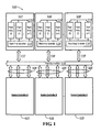
- FIG. 1 is a diagram illustrating an architecture of a large network of memory systems comprising a plurality of flash memory modules and system controllers interconnected via a flashbus according to an embodiment of the invention.
- a network of memory system i.e., system 100 or apparatus 100
- a network of memory system comprising a plurality of system controllers 101 to 103 that may be implemented as, for example, system-on-chip (SoC), although other technologies may be used for the system controllers 101 - 103 .
- SoC system-on-chip
- the system 100 also includes a plurality of flash memory modules 107 , 108 and 109 that is attached to (coupled to) the system controllers 101 to 103 through the communication bus interface 116 (e.g., a flashbus interface).
- a flashbus interface can be any different types of communication bus interfaces and is not limited to only a flashbus interface.
- system 100 is illustrated as including three system controllers ( 101 , 102 and 103 ), and with flash memory modules ( 107 , 108 and 109 ), any number of system controllers and flash memory modules may be used in the various embodiments shown in the drawings.
- the system controllers A 101 to N 103 can be implemented as, but not limited to an integrated circuit, a module, a die or a system-on-chip (SoC) wherein each system controller communicates the memory specific transactions to the flash memory modules 107 , 108 and 109 .
- SoC system-on-chip
- the flash memory modules 107 , 108 and 109 contain (or include) a plurality of flash arrays 110 , 112 , and 114 , respectively.
- the flash arrays 110 , 112 , and 114 may be, for example, flash memory devices, chips, and/or die 110 , 112 and 114 (hereinafter “flash devices/chips/die” 110 , 112 , and 114 ).
- flash devices/chips/die are attached to (coupled to) the flash array controllers 111 , 113 and 115 , respectively.
- the flash array controllers are not dependent on the number of flash devices/chips/die connected to the flash array controllers, and the flash devices/chips/die in a flash memory module (e.g., module 106 , 108 , and/or 109 ) may vary in number. Therefore, the flash memory modules 107 , 108 and 109 provide the respective flash array controllers 111 , 112 and 113 that communicates between the system controllers 101 , 102 and 103 and a potential unlimited number of flash devices/chips/die 110 , 112 and 114 via the flashbus interface 116 .
- a flash memory module e.g., module 106 , 108 , and/or 109
- Each flash array controllers 111 , 113 and 115 can drive a first plurality of communications buses (e.g., flashbuses) that includes the communication buses (e.g., flashbuses) 117 , 118 and 119 simultaneously.
- a flashbus can be any different types of communication bus and is not limited to only a flashbus.
- the flash memory modules 107 , 108 and 109 are coupled to the flash bus interface 116 by the first plurality of flashbuses 117 , 118 , and 119 , respectively.
- the memory transactions from the system controllers 101 , 102 and 103 are transmitted to a designated flash memory module among the flash memory modules 107 , 108 and 109 via the flashbus interface 116 .
- the communication bus interface (e.g., flashbus interface) 116 contains (or includes) a second plurality of communication buses (e.g., flashbuses) 104 , 105 and 106 that interconnects the system controllers 101 , 102 , and 103 , respectively, to the flashbus interface 116 .
- the flashbus interface 116 herein supports the transfer of commands, address bytes, receive and transmit command, status, response, address and data bytes, other hand-shaking related signals, and/or other memory transaction-related signals, between the I/O device(s) 202 ( FIG. 2 ) and the flash memory modules 107 - 109 .
- U.S. Pat. No. 8,447,908 is hereby fully incorporated herein by reference.
- flash device memory device
- flash bus single memory bus
- select lines may be used.
- the number of data buses or FIFOs used is also not intended to be limiting. As would be evident to one of ordinary skill having the benefit of this disclosure, using more than one data bus, FIFO, or both, increases the available pathways through which data may be transmitted between I/O device(s) 202 ( FIG. 2 ) and flash device interface 116 .
- FIG. 2 is a diagram illustrating one possible embodiment of a system controller according to an embodiment of the invention.
- This system controller 200 can be any (or each) of the system controllers 101 - 103 in FIG. 1 .
- the system controller 200 is implemented as a system for controlling memory transactions.
- the system controller 200 may comprise a processor 201 , one or more input/output devices 202 and one or more memory module controllers 203 , 204 and 205 , where the processor 201 , devices 201 and memory module controllers 203 - 205 are interconnected via a local bus interface 218 .
- the number of I/O devices 202 and memory module controllers may vary.
- the number of processor in the system controller 200 may also vary.
- the system controller 200 may include the processors 201 and 260 or any other plurality of processors connected to the local bus interface 218 , or the system controller 200 may only include the single processor 201 .
- the system controller 200 may be implemented, but not limited to, in any of the following technologies: discrete logic circuits capable of memory transaction, an application specific integrated circuit having appropriate combinational and sequential logic gates implemented on a system-on-chip (SoC).
- SoC system-on-chip
- the local bus interface 218 may include one or more bus lines.
- the system may also include other elements such as local buffers or cache, sub-controllers, and the like.
- the local bus interface 218 includes a first plurality of local bus lines 227 that couples the I/O devices 202 and processor 201 (and processor 260 ) to the local bus interface 218 , and includes a second plurality of local bus lines 229 that couples the local bus interface 218 to the memory module controllers 203 , 204 , and 205 .
- the memory module controllers 203 - 205 of the system controller 200 includes the following components: (a) one or more DMA (Direct Memory Access) controllers or flash-specific DMA controllers 206 , 207 and 208 , respectively; (b) bus controller 209 , 210 and 211 that manages the external flashbus 219 , 220 and 221 , respectively; (c) arbiters 215 , 216 and 217 , respectively, if a plurality of flash specific DMA controllers is implemented.
- DMA Direct Memory Access
- the local processor 201 sends a command 230 to the any of the flash specific DMA controllers 206 , 207 or 208 of any memory module controller 203 , 204 or 205 , respectively.
- the flash specific DMA controllers e.g., DMA controller 206 a
- the flash specific DMA controller 206 a upon receiving the command 230 will convert the command 230 into flash-specific native commands 233 and then transmits the native commands 233 to the flash devices/chips/die 110 - 109 ( FIG. 1 ) in sequence of reads, writes or erases data, and the like.
- the arbiter 215 can be added.
- the arbiter 215 receives (and processes) an arbitration request 236 from one of the DMA controllers 206 for access to the flashbus 219 by the DMA controller 206 that sent the arbitration request 236 .
- the flashbus 219 is coupled to the flashbus interface 116 .
- the arbitration method performed by the arbiter 215 can be, for example, but not limited to the following: round robin arbitration, centralized arbitration, distributed arbitration, or another arbitration method.
- the memory module controllers 203 , 204 and 205 include the bus controllers 209 , 210 , and 211 , respectively.
- the bus controllers 209 , 210 , and 211 drive the flashbuses 219 , 220 , and 221 , respectively, in the second plurality of flashbuses 104 ( FIG. 1 ).
- the flashbuses 219 , 220 , and 221 can only service one of the DMA controllers 206 , 207 , and 208 , respectively, at a time.
- These flashbuses 219 , 220 , and 221 are used to communicate to the flash memory module controllers 203 , 204 and 205 , respectively.
- FIG. 3 is a diagram illustrating an embodiment of the memory module controller contained (included) in a system controller according to an embodiment of the present invention.
- This system controller 300 can be any of the system controllers 101 - 103 in FIG. 1 .
- the system controller 300 presented herein has at least some of the similar components that are in the system controller 200 illustrated in FIG. 2 , although the block diagram in FIG. 3 highlights another embodiment of the structural design and configuration of the memory module controllers 203 , 204 and 205 of a system controller in FIG. 2 .
- the system controller 300 includes a processor 301 , one or more input/output devices 302 and a plurality of memory module controllers 303 , 304 , 305 , 306 , 307 , and 308 which are all attached (coupled) to the flashbus interface 3 - 116 (which is similar to the flashbus interface 116 in FIG. 1 ). As similarly noted above, the system controller 300 may include more than one processor 301 .
- Each memory module controller 303 to 308 may comprise any, but not limited to the following devices: (a) one or more flash specific DMA controllers 315 to 320 , respectively, which can be custom made or commercially available and capable of initiating memory transactions and (b) bus controllers 309 to 314 , respectively, capable of managing the flashbus and bus arbitration mechanism (configuration and/or method) wherein an arbiter can be incorporated into the bus controller or can be a separate individual module that can be added to each of the memory module controllers 303 to 308 . Note that in FIG.
- the arbiters 215 , 216 , and 217 are separate individual modules that are coupled to the DMA controllers 206 , 207 , and 208 , respectively, and the arbiters 215 , 216 , and 217 are also included in the memory module controllers 203 , 204 , and 205 , respectively. Therefore, an arbiter (similar to the arbiters 215 , 216 , or 217 of FIG. 2 ) can also be coupled to any or each of the DMA controllers 303 - 308 . For example, an arbiter 370 can be coupled to the DMA controllers 316 . Similarly, other separate arbiters (not shown in FIG. 3 ) can be coupled to the DMA controllers 315 , 317 , 318 , 319 , and 320 , respectively.
- Any of the memory module controllers 303 to 308 can also be implemented, but not limited to, any or a combination of the following technologies: a state machine, a discreet logic circuit capable of performing memory transactions, an application specific integrated circuit (ASIC) having appropriate combinational and sequential logic gates, and/or other technologies.
- a state machine a discreet logic circuit capable of performing memory transactions
- ASIC application specific integrated circuit
- FIG. 3 highlights the scheme or architecture of how the system controller 300 can be attached to the flashbus interface 116 of the system 100 shown in FIG. 1 .
- the system controller 300 is configured to provide a dual-memory module controller stages 321 , 322 and 323 .
- the stage 321 includes the memory module controllers 303 and 304 .
- the stage 322 includes the memory module controllers 305 and 306 .
- the stage 323 includes the memory module controllers 307 and 308 .
- Each memory module controller 309 , 310 , 311 , 312 , 313 , and 314 drives a flashbus 324 , 325 , 326 , 327 , 328 , and 329 , respectively.
- the second plurality of flashbuses 324 , 325 , 326 , 327 , 328 , and 329 are coupled to the flashbus interface 3 - 116 , while the first plurality of flashbuses 3 - 117 through 3 - 119 are also coupled to the flashbus interface 3 - 116 .
- the flash memory modules 3 - 107 through 3 - 109 are coupled via the first plurality of flashbuses 3 - 117 through 3 - 119 , respectively, to the flashbus interface 3 - 116 .
- each dual memory module controller stages 321 - 323 provides a dual flashbus connection to the flashbus interface 3 - 116 and each dual-flashbus is connected to one or more flash memory module 3 - 117 through 3 - 119 via the flashbus interface 3 - 116 .
- the dual memory module controller stage 321 is coupled to (and drives) the first pair of flashbuses 324 and 325 and provides a dual flash bus connection to the flashbus interface 3 - 116 via the first pair of flashbuses 324 and 325 .
- the dual memory module controller stage 322 is coupled to (and drives) the second pair of flashbuses 326 and 327 and provides a dual flash bus connection to the flashbus interface 3 - 116 via the second pair of flashbuses 326 and 327 .
- the dual memory module controller stage 323 is coupled to (and drives) the third pair of flashbuses 328 and 329 and provides a dual flash bus connection to the flashbus interface 3 - 116 via the third pair of flashbuses 328 and 329 .
- the number of dual memory memory module controller stages may vary in the system controller 300 , and the number of respective pairs of flashbuses coupled to and driven by respective dual memory module controller stages.
- the system controller 300 includes the dual-memory module controller stages 321 , 322 and 323 .
- the number of dual-memory module controller stages in the system controller 300 may vary in number from one dual-memory module controller stage to any given plurality of dual-memory module controller stages.
- the system controller 300 can include four or more dual-memory module controller stages.
- the first dual memory module controller stage 321 includes the first pair of two memory module controllers 303 and 304 driving the first pair of two flashbuses 324 and 325 , respectively.
- a first memory module controller 303 is provided such that it includes a first plurality of DMA controllers 315 attached to a first bus controller 309 which drives the first flashbus 324 .
- a second (or secondary) memory module controller 304 is provided and also includes a second plurality of DMA controllers 316 attached to a second bus controller 310 for driving the second flashbus 325 .
- the second dual memory module controller stage 321 includes the second pair of two memory module controllers 305 and 306 driving the second pair of two flashbuses 326 and 327 , respectively.
- a third memory module controller 305 is provided such that it includes a third plurality of DMA controllers 317 attached to a third bus controller 311 which drives the third flashbus 326 .
- a fourth memory module controller 306 is provided and also includes a fourth plurality of DMA controllers 318 attached to a fourth bus controller 312 for driving the fourth flashbus 327 .
- the third dual memory module controller stage 323 includes the third pair of two memory module controllers 307 and 308 driving the third pair of two flashbuses 328 and 329 , respectively.
- a fifth memory module controller 307 is provided such that it includes a fifth plurality of DMA controllers 319 attached to a fifth bus controller 313 which drives the fifth flashbus 328 .
- a sixth memory module controller 308 is provided and also includes a sixth plurality of DMA controllers 320 attached to a fifth bus controller 314 for driving the fifth flashbus 329 .
- the system controller 300 can be attached (coupled) to one or more flash memory modules 3 - 107 through 3 - 109 by one or more flashbuses 324 to 329 .
- This mechanism provides a redundancy path for the system controller 300 when the flashbus 324 fails (or at least another one of the flashbuses 325 - 329 fails). So if the system controller 300 is connected to flash memory module(s) 330 using flashbuses 324 and 325 , when one or more flashbuses (e.g., flashbus 324 and/or 325 ) fails to operate, the system controller 300 can still access flash memory module(s) 330 by using a surviving flashbus.
- flashbus 324 fails, then the flashbuses 325 - 329 are surviving flashbuses. If flashbus 324 and 325 fail, then the flashbuses 326 - 329 are surviving flashbuses. A surviving flashbus permits the I/O device(s) 302 to access any of the flash memory module(s) 330 even if one or more of the flashbuses 324 - 329 fails as long as there is a surviving (non-failing) flashbus among the flashbuses 324 - 329 .
- This mechanism expands the access of a system controller 300 to a plurality of flash array modules 330 .
- the memory module controllers 303 and 304 are attached to a sub-controller/configuration device 331 that manages the configuration or settings of the memory module controllers 303 and 304 .
- the sub-controller 331 is illustrated as controlling the dual-memory module controllers 321 , one or more memory module controllers ( 303 or 304 ) may be used.
- the sub-controller/configuration device 331 manages the memory module controllers 303 and 304 and bus controllers 309 and 310 .
- the sub-controller/configuration device 331 is capable of selecting a redundant path for the operation performed by the dual memory module controller stage 321 and send control signals 332 to the bus controllers 309 or 310 .
- the sub-controller/configuration device 331 can detect the failure of the buses 324 and 325 driven by memory controllers 303 and 304 , respectively, and therefore providing the dual-memory module controller 321 a redundant path either using the flashbus 324 or flashbus 325 .
- the stages 321 - 323 are coupled to the bus interface 3 - 218 (similar to bus interface 218 in FIG. 2 ) via the plurality of buses 3 - 229 and the I/O device(s) 302 and processor 301 are coupled to the bus interface 3 - 218 via the plurality of buses 3 - 227 , similarly described above with reference to FIG. 2 .
- the sub-controller/configuration device 331 can detect the failure of the buses 324 and 325 by a standard bus handshaking protocol so as to detect any failure of the buses 324 and 325 .
- a bus handshaking protocol for example, the subcontroller/configuration device 331 can send a “Hello” signal to the flash memory modules 330 via each of the bus 324 and 325 and can determine if there is any failure of the bus 324 and/or 325 is an “ack” acknowledgement signal is received (or is not received) by the subcontroller/configuration device 331 from the flash memory modules 330 in response to the Hello signals.
- the system controller 300 may alternatively use other handshaking protocols to detect for failures in any of the buses 324 , 325 , 326 , 327 , 328 , and 329 .
- sub-controller/configuration device 331 If the sub-controller/configuration device 331 detects the failure of one of the buses 324 and 325 , then sub-controller/configuration device 331 sends the control signal 332 that disables the memory module controller 303 so that the surviving bus (and the associated memory module controller of the surviving bus) will allow the I/O device(s) to access the flash memory modules 330 .
- the sub-controller/configuration device 331 detects a failure of the bus 324 , then the sub-controller/configuration device 331 sends the control signal to the memory module controller 303 so that the memory module controller 303 is disabled, and the memory module controller 304 will process all commands and data and signals to and from the I/O device(s) 301 and processor 301 (including the command 330 from the processor 301 so that a memory transaction is initiated) and use the bus 325 for access to the flash memory module(s) 330 .
- each set of the dual memory module controller stages 321 , 322 and 323 can be separately attached to a flash memory module 330 .
- a system controller 300 can control a plurality of flash memory module(s) 330 using sets of memory module controllers 321 to 323 for driving a plurality of flashbuses per flash memory module and providing a parallel operation of memory transaction via at least some of the buses 324 - 329 and via at least some of the buses 3 - 117 through 3 - 119 .
- any of the dual-memory module controllers 321 , 322 , and 323 and subcontroller/configuration devices 331 , 360 , and 362 , respectively, can be included (or implemented) in an embodiment of the system controller 200 of FIG. 2 .
- FIG. 4 is a diagram illustrating an embodiment of the flash memory module 400 according to an embodiment of the invention.
- the flash memory module 400 includes a flash array controller 406 that provides an interface between flash devices/chips/die 401 through 405 and flashbus interface 413 .
- Each flash devices/chips/die 401 - 405 may include different vendors of flash devices. Each flash devices/chips/die 401 - 405 of the flash memory module 400 may be used or owned by one or more system controllers 414 or 415 . The flash devices/chips/die 401 - 405 and/or system controllers 414 - 415 may vary in number.
- the flash array controller 406 receives the system commands 450 transmitted by the system controller 410 and 411 .
- the flash array controller 406 generally converts the system commands 450 into flash specific commands 455 that can be transmitted by the flash array controller 406 to one or more flash devices 401 - 405 via the flash memory bus 412 .
- the flash specific commands 455 trigger flash operations such as read, write, erase, and/or other memory-related operations.
- the flash memory bus 412 also typically includes address and data lines and other controls signals such as Write Enable, Chip Enable, and/or other lines or signals.
- the flash array controller 406 may be a separate integrated system from the memory devices 401 - 405 .
- the flash memory module 400 can be attached to one or more system controllers 414 and 415 . This is due to the fact that each or any group of flash devices/chips/die 401 - 405 can be used as a storage area of a particular system controller 414 and 415 .
- a flash array controller 406 provides expander ports 460 that can allow the flash memory module 400 to be connected to a second controller, third controller, and the like system controllers such as the system controllers 414 and 415 .
- the system controllers 414 or 415 may be similar in architecture to the system controller 200 in FIG. 2 or the system controller 300 in FIG. 3 .
- the flashbuses 407 and 408 of flash memory module 400 are connected to the system controller 414 , and then flashbus 409 is connected to the system controller 415 .
- One or more flashbuses 407 - 409 can be connected to a single system controller (controller 414 or 415 ) or a plurality of system controllers 414 or 415 .
- the connection between a flash memory module 400 and the system controller 415 includes two or more flashbus lines to provide a redundant path in the event that one or more bus fails.
- the flash memory module 400 and the system controller 415 may be connected via, for example, the flashbus lines 410 and 411 and also connected via the flashbus interface 413 .
- This failover scheme and redundant path feature is, for example, disclosed in commonly-assigned and commonly-owned U.S. Patent Application entitled “Bus Arbitration With Routing and Failover Mechanism” 14/216,627 which is hereby fully incorporated herein by reference.
- FIG. 5 is a diagram illustrating one embodiment of a network of memory systems according to the present invention.
- the system 500 comprising two flash memory modules 501 and 502 which are attached to the system controllers 503 and 504 .
- the number of flash memory modules and system controllers may vary.
- a flash memory module 501 includes a first plurality of flash devices/chips/die 505 , 506 , 507 , and 509 which are attached to a first flash array controller 514 via first plurality of flash memory buses 516 .
- a second flash memory module 502 includes a second plurality of flash devices/chips/die 510 , 511 , 512 , and 513 which are attached to a second flash array controller 515 via the second plurality of flash memory buses 517 .
- Each flash memory module 501 and 502 is attached to the system controllers 503 and 504 via the flashbus interface 518 which is presented herein as (or including) a plurality of flashbuses 523 , 524 , 525 , and 526 and 531 , 532 , 533 , and 534 .
- the system controllers 503 or 504 can be similar to any of the embodiments of the system controllers disclosed in FIGS. 1-3 above.
- the system controller 503 includes the processor 301 a and I/O devices 302 a and memory module controllers 519 , 520 , 521 , and 522 .
- the system controller 504 includes the processor 301 b and I/O devices 302 b and memory module controllers 527 , 528 , 529 , and 530 .
- the flash devices/chips/die 506 and 507 are omitted in the flash memory module 501 , and/or the flash devices/chips/die 511 and 512 are omitted in the flash memory module 502 .
- the flash memory module 501 includes a first plurality of flash devices/chips/die 505 and 509 which are attached to the first flash array controller 514 via first plurality of flash memory buses 516 .
- the second flash memory module 502 includes the second plurality of flash devices/chips/die 510 and 513 which are attached to the second flash array controller 515 via the second plurality of flash memory buses 517 .
- Each flash memory module 501 and 502 is attached to the system controllers 503 and 504 via the flashbus interface 518 which is presented herein as (or including) a plurality of flashbuses 523 and 525 and 532 and 534 .
- the ownership of the flash devices/chips/die 505 - 509 and 510 - 513 is distributed such that the memory module controllers 519 - 522 and 527 - 530 from system controllers 503 and 504 , respectively, can control or access any of the flash devices 505 - 509 and 510 - 513 from the flash memory modules 501 and 502 , respectively.
- the first system controller 503 contains (includes) a first plurality of four memory module controllers 519 - 522 , and the memory module controllers 519 - 522 are coupled to and drive the flashbuses 523 - 526 , respectively.
- the second system controller 504 contains (includes) a second plurality of four memory module controllers 527 - 530 , and the memory module controllers 527 - 530 are coupled to and drive the flashbuses 531 - 534 , respectively.
- flash memory module 501 Assuming, for example, that flash devices/chips/die 505 and 509 are controlled by the memory module controllers 519 and 520 , the connection between flash memory module 501 and system controller 503 is therefore established using the flashbuses 523 and 524 .
- a preferred embodiment of the present invention includes that the interconnection between system controller 503 and flash memory module 501 should have at least two communication lines to promote redundant and fault-tolerant connection so that access to the flash memory module 501 is possible via a surviving flashbus (e.g., flashbus 523 ) if the other one (e.g., flashbus 524 ) fails.
- Part of the control signals 560 transmitted by the memory module controllers 519 and 520 is an identification code 561 that indicates to what flash memory bus 516 does the intended flash device array 505 or 509 is connected to.
- the flash array controller 514 of the flash memory module 501 is capable of translating this code 561 in order to determine the flash memory bus 516 that is connected to the target flash device array. For example, the flash array controller 514 translates the code 561 so that the flash array controller 514 determines that a memory transaction 570 from the memory module controller 519 is directed via the flash bus 516 a to the target flash array 505 .
- a further aspect of an embodiment of the present invention includes that the system controller 503 can control a plurality of flash memory modules, which in this case, aside from controlling the first flash memory module 501 , system controller 503 is also connected to (and controls) the second flash memory module 502 .
- the memory module controllers 521 and 522 controls the flash devices/chips/die 511 and 512 .
- the system controller 503 uses the flashbuses 525 and 526 to communicate with the flash memory module 502 .
- the second flash array controller 515 receives control signals 562 with an identification code 563 from the memory module controllers 521 and 522 to identify from what flash memory bus 517 does the intended flash devices/chips/die 511 and 512 are attached to. For example, the flash array controller 515 translates the code 563 so that the flash array controller 515 determines that a memory transaction 570 from the memory module controller 521 is directed via the flash bus 517 a to the target flash array 510 .
- the method and apparatus for system controller 504 is similar to system controller 503 as discussed above.
- Memory module controllers 527 and 528 control the flash devices/chips/die 506 and 507 of the first flash memory module 501 .
- the flashbuses 531 and 532 are established by the memory module controllers 527 and 528 , respectively.
- the flash devices/chips/die 510 and 513 are controlled by memory modules 529 and 530 .
- the flashbuses 533 and 534 are established by the memory module controllers 529 and 530 , respectively.
- the flash array controller 515 of the flash memory module 502 make use of the identification code 565 (in the control signals 566 ) sent by the memory modules 529 and 530 to identify which flash memory bus 515 does the intended flash devices/chips/die 510 and 513 are attached to. For example, the flash array controller 515 translates the code 565 so that the flash array controller 515 determines that a memory transaction 570 from the memory module controller 529 is directed via the flash bus 517 b to the target flash array 512 .
- the flash array controller 514 translates identification codes received from flash busses 524 and 526 to determine the target flash arrays of memory transactions 570 . Similarly, the flash array controller 515 translates identification received codes from flash busses 531 , 532 , and 534 to determine the target flash arrays of memory transactions 570 .
- FIG. 6 is a block diagram of an architecture of a large network of memory systems, in accordance with an embodiment of the invention.
- This system (apparatus) 600 comprises a plurality of flash memory modules interconnected with other flash memory modules and to a system controller 610 via a point-to-point flashbus topology.
- the system controller 610 is similar in functionality and structure as any of the system controllers described above with reference to the above-identified drawings.
- the flashbus controllers 630 - 635 can receive and transmit command, status, response, address and data bytes to and from the system controller 610 .
- the flashbus controllers 630 - 635 can also receive and transmit command, status, response, address and data bytes to and from adjacent flash memory modules 670 - 675 .
- the Flashbus Point-to-Point Lines includes a channel used to connect system controller 610 to/from flash memory modules 670 - 675 and a channel used to connect flash memory modules to/from other flash memory modules.
- a channel includes a first plurality of point-to-point lines 660 - 661 and 636 - 635 that connects the system controller 610 to/from flash memory modules (e.g., flash memory modules 670 and 673 ).
- the number of point-to-point lines in this first plurality of lines may vary.
- a channel includes a second plurality of point-to-point lines 662 - 663 , 664 - 655 , 638 - 639 , and 640 - 641 .
- the number of point-to-point lines in this second plurality of lines may vary.
- the lines 662 - 663 connect the modules 670 and 671
- the lines 664 - 665 connect the modules 671 and 672
- the lines 638 - 639 connect the modules 673 - 674
- the lines 640 - 641 connect the modules 674 - 675 .
- the point-to-point lines described herein can be, for example, flashbuses.
- Flashbus Shared Lines 642 and 643 are as follows. Some embodiments of the invention use these share lines 642 and/or 643 for sideband signaling such as, by way of example but not limited to arbitration, messaging, protocol handshakes.
- the flashbus shared lines 642 and 643 may include an optional channel used to connect system controller 610 to/from flash memory modules 670 - 675 , and an optional channel used to connect flash memory modules to/from other flash memory modules.
- the flashbus shared lines 642 and 643 are omitted and not used for communications.
- Flash Array Controllers 650 through 655 are similar in functionality and structure as any of the flash array controllers described above with reference to the above-identified drawings.
- Flash Array 690 - 695 is similar in functionality and structure as any flash array described above with reference to the above-identified drawings.
- Flash Modules 670 - 675 are similar in functionality and structure as any of the flash modules described above with reference to the above-identified drawings.
- the Flashbus Chain comprises: (a) the system controller 610 connected point-to-point to an adjacent flashbus controller A and the adjacent flashbus controller A is connected to an adjacent flashbus controller B, wherein the system controller 610 communicates to the flashbus controller B by sending and receiving information via the flashbus controller A.
- the system controller 610 communicates to the flashbus controller 631 by sending and receiving information via the flashbus controller 630 so that information is communicated between the system controller 610 and the flashbus controller 631 .
- the Flashbus Chain alternatively comprises: a flashbus controller A connected point-to-point to an adjacent flashbus controller B, wherein the adjacent flashbus controller B may be connected to an adjacent flashbus controller C. and so on.
- the Flashbus Chain alternatively comprises a flashbus controller 633 connected point-to-point to an adjacent flashbus controller 634 , and the adjacent flashbus controller 634 may be connected to an adjacent flashbus controller 635 , and so on.
- the nodes of the chain communicate with each other through the adjacent nodes of the chain (system controllers and/or flashbus controllers).
- system controller 610 , flashbus controller 630 , flashbus controller 631 , flashbus controller 632 forms a flashbus chain of 4 nodes.
- flashbus controller 630 and flashbus controller 631 form a flashbus chain of 2 nodes.
- System Controller 610 communicates with Flash Array Controller 650 via FlashBus Controller 630 .
- System Controller 610 communicates with Flash Array Controller 651 via FlashBus Controller 630 and FlashBus Controller 631 .
- FlashBus Controller 630 identifies either via information from Flashbus Shared Lines 642 or information from the incoming command, status, response, address and data bytes from the Flashbus Point-to-Point Lines 660 that the incoming command, status, response, address and data bytes is not intended for the Flash module 670 .
- the Flashbus controller 630 then passes the aforementioned command, status, response, address and data bytes to the adjacent FlashBus Controller 631 associated with Flash Module 671 via the Flashbus Point-to-Point Lines 662 .
- FlashBus Controller 631 identifies either via information from Flashbus Shared Line 642 or information from the incoming command, status, response, address and data bytes from the Flashbus Point-to-Point Lines 662 that the incoming command, status, response, address and data bytes is intended for the Flash module 671 . Flashbus controller 631 then communicates with the Flash Array Controller 651 accordingly.
- System Controller 610 communicates with Flash Array Controller 652 via FlashBus Controller 630 , FlashBus Controller 631 , and FlashBus Controller 632 .
- FlashBus Controller 630 identifies either via information from Flashbus Shared Lines 642 or information from the incoming command, status, response, address and data bytes from the Flashbus Point-to-Point Lines 660 that the incoming command, status, response, address and data bytes is not intended for the Flash module 670 .
- the Flashbus Controller 630 then passes the aforementioned command, status, response, address and data bytes to the adjacent FlashBus Controller 631 associated with Flash Module 671 via the Flashbus Point-to-Point Lines 632 .
- FlashBus Controller 631 identifies either via information from Flashbus Shared Lines 642 or information from the incoming command, status, response, address and data bytes from the Flashbus Point-to-Point Lines 662 that the incoming command, status, response, address and data bytes is not intended for the Flash module 671 .
- the Flashbus Controller 631 then passes the said command, status, response, address and data bytes to the adjacent FlashBus Controller 632 associated with Flash Module 672 via the Flashbus Point-to-Point Lines 664 .
- FlashBus Controller 632 identifies either via information from Flashbus Shared Line 642 or information from the incoming command, status, response, address and data bytes from the Flashbus Point-to-Point Lines 664 that the incoming command, status, response, address and data bytes is intended for the Flash module 672 . Flashbus controller 632 then communicates with the Flash Array Controller 652 accordingly. Therefore, system controller 610 is able to communicate with the flash module 672 . Additionally, in this example, the Flashbus Controllers 630 and 631 serve as a transmission conduit in the communication to the Flash module 672 .
- the above example uses the communication path comprising Flashbus Point-to-Point Lines 660 , 662 , and up to and until 664 .
- an alternate path can use the communication path comprising Flashbus Point-to-Point Lines 631 , 662 , and up to and until 655 .
- Flashbus point-to-point line 632 is faulty, the communication path from the system controller 810 to Flash module 672 can be Flashbus Point-to-Point Lines 630 , 633 , and up to and until 664 .
- the communication path from the system controller 610 to Flash module 672 can be any of the following:
- the above alternative communication paths provide a fault tolerant mechanism in the system 600 .
- the Flashbus Controllers 630 , 631 to 635 can pass the incoming command, status, response, address and data bytes to the adjacent Flash controller via cutthrough, store forward, or buffering.
- FIG. 7 is a block diagram of an architecture of a large network of memory systems, in accordance with another embodiment of the invention.
- the system 700 comprises a plurality of flash memory modules interconnected to other flash memory modules and to a plurality of system controllers (e.g., controllers 710 , 711 , and 712 ) via a point-to-point flashbus topology.
- the number of system controllers can vary in number from two or more system controllers.
- the system controllers 710 - 712 are similar in functionality and structure as any of the system controllers described above with reference to FIG. 6 .
- the Flashbus Controllers 730 - 735 are similar in functionality and structure as any of the flashbus controllers described above with reference to FIG. 6 .
- Flashbus Point-to-Point Lines 780 - 788 and 739 - 747 are similar in functionality and structure as any of the Flashbus Point-to-Point Lines described above with reference to FIG. 6 .
- the Flashbus Shared Lines 790 - 792 and 793 - 795 are similar in functionality and structure as any of the Flashbus Shared Lines described above with reference to FIG. 6 .
- Flash Array Controllers 750 - 755 are similar in functionality and structure as any of the flash array controllers described above with reference to FIG. 6 .
- Any Flash Array 760 - 765 are similar in functionality and structure as any of the flash arrays described above with reference to FIG. 6 .
- the Flash Modules 770 - 775 are similar in functionality and structure as any of the flash modules described above with reference to FIG. 6 .
- a Flashbus Chain in FIG. 7 is similar in functionality and structure as any of the example flashbus chains described above with reference to FIG. 6 .
- System Controller 710 communicates with Flash Array Controller 750 via FlashBus Controller 730 .
- System Controller 710 communicates with Flash Array Controller 751 via FlashBus Controller 730 and FlashBus Controller 731 .
- FlashBus Controller 730 identifies either via information from Flashbus Shared Lines 790 or information from the incoming command, status, response, address and data bytes from the Flashbus Point-to-Point Lines 760 that the incoming command, status, response, address and data bytes is not intended for the Flash module 770 .
- the Flashbus Controller 730 then passes the aforementioned command, status, response, address and data bytes to the adjacent FlashBus Controller 731 associated with Flash Module 771 via the Flashbus Point-to-Point Lines 783 .
- FlashBus Controller 731 identifies either via information from Flashbus Shared Lines 790 or information from the incoming command, status, response, address and data bytes from the Flashbus Point-to-Point Lines 783 that the incoming command, status, response, address and data bytes is intended for the Flash module 771 . Flashbus controller 731 then communicates with the Flash Array Controller 751 accordingly. Therefore, system controller 710 is able to communicate with the flash module 771 . Additionally, in this example, the Flashbus Controller 730 serves as a transmission conduit in the communication to the Flash module 771 .
- System Controller 710 communicates with Flash Array Controller 752 via FlashBus Controller 730 , FlashBus Controller 731 , and FlashBus Controller 732 .
- FlashBus Controller 730 identifies either via information from Flashbus Shared Lines 790 or information from the incoming command, status, response, address and data bytes from the Flashbus Point-to-Point Lines 780 that the incoming command, status, response, address and data bytes is not intended for the Flash module 770 .
- the Flashbus Controller 730 then passes the aforementioned command, status, response, address and data bytes to the adjacent FlashBus Controller 731 associated with Flash Module 771 via the Flashbus Point-to-Point Lines 783 .
- FlashBus Controller 731 identifies either via information from Flashbus Shared Lines 790 or information from the incoming command, status, response, address and data bytes from the Flashbus Point-to-Point Lines 783 that the incoming command, status, response, address and data bytes is not intended for the Flash module 771 .
- the Flashbus Controller 731 then passes the above-mentioned command, status, response, address and data bytes to the adjacent FlashBus Controller 732 associated with Flash Module 772 via the Flashbus Point-to-Point Lines 786 .
- FlashBus Controller 732 identifies either via information from Flashbus Shared Line 790 or information from the incoming command, status, response, address and data bytes from the Flashbus Point-to-Point Lines 786 that the incoming command, status, response, address and data bytes is intended for the Flash module 772 . Flashbus controller 732 then communicates with the Flash Array Controller 752 accordingly.
- the communication path used comprises Flashbus Point-to-Point Lines 780 , 783 , and up to and until 786 .
- a similar set of interactions may occur for when System Controller 711 communicates with Flash Array Controller 752 .
- the communication path comprises Flashbus Point-to-Point Lines 781 , 784 , and up to and until 787 .
- a similar set of interactions may occur for when System Controller 712 communicates with Flash Array Controller 752 .
- the communication path comprises Flashbus Point-to-Point Lines 782 , 785 , and up to and until 768 .
- each of the System Controllers 710 , 711 , and 712 has access to all Flash devices 760 , 761 , 762 , 763 , 764 , and 765 contained in Flash modules 770 , 771 , 772 , 773 , 774 , 775 , respectively, and so on.
- Flashbus point-to-point line 783 is faulty, the communication path from the system controller 710 to Flash module 772 can be Flashbus Point-to-Point Lines 780 , 784 , up to and until 786 .
- the communication path from the Flashbus controller 730 to adjacent Flashbus controller 731 can be any of the Flashbus Interfaces 783 , 784 , 785 .
- the communication path from the Flashbus controller 731 to adjacent Flashbus controller 732 can be any of the Flashbus Interfaces 786 , 787 , 788 .
- the communication path from the System Controller 710 to the Flash module 772 is a combination of the above mentioned Flashbus Interfaces, in as long as they are working (i.e. not faulty).
- the Flashbus Controller 730 , 731 to 732 can pass the incoming command, status, response, address and data bytes to the adjacent Flash controller via cutthrough, store forward, or buffering.
- system controller 710 communicates with FlashBus Controller 755 via FlashBus Controller 733 , FlashBus Controller 734 , and FlashBus Controller 735 .
- FlashBus Controller 733 identifies either via information from Flashbus Shared Lines 793 or information from the incoming command, status, response, address and data bytes from the Flashbus Point-to-Point Lines 739 that the incoming command, status, response, address and data bytes is not intended for the Flash module 773 .
- the Flashbus Controller 733 then passes the aforementioned command, status, response, address and data bytes to the adjacent FlashBus Controller 734 associated with Flash Module 774 via the Flashbus Point-to-Point Lines 742 .
- FlashBus Controller 734 identifies either via information from Flashbus Shared Lines 793 or information from the incoming command, status, response, address and data bytes from the Flashbus Point-to-Point Lines 742 that the incoming command, status, response, address and data bytes is not intended for the Flash module 774 .
- the Flashbus Controller 734 then passes the above-mentioned command, status, response, address and data bytes to the adjacent FlashBus Controller 735 associated with Flash Module 775 via the Flashbus Point-to-Point Lines 745 .
- FlashBus Controller 735 identifies either via information from Flashbus Shared Line 793 or information from the incoming command, status, response, address and data bytes from the Flashbus Point-to-Point Lines 745 that the incoming command, status, response, address and data bytes is intended for the Flash module 775 . Flashbus controller 735 then communicates with the Flash Array Controller 755 accordingly.
- the communication path used comprises Flashbus Point-to-Point Lines 739 , 742 , and up to and until 745 .
- a similar set of interactions may occur for when System Controller 711 communicates with Flash Array Controller 775 .
- the communication path comprises Flashbus Point-to-Point Lines 740 , 743 , and up to and until 746 .
- a similar set of interactions may occur for when System Controller 712 communicates with Flash Array Controller 775 .
- the communication path comprises Flashbus Point-to-Point Lines 741 , 744 , and up to and until 747 .
- each of the System Controllers 710 , 711 , and 712 has access to all Flash devices 760 , 761 , 762 , 763 , 764 , and 765 contained in Flash modules 770 , 771 , 772 , 773 , 774 , 775 , respectively, and so on.
- Flashbus point-to-point line 742 If Flashbus point-to-point line 742 is faulty, the communication path from the system controller 710 to Flash module 775 can be Flashbus Point-to-Point Lines 739 , 743 , up to and until 745 .
- the communication path from the Flashbus controller 733 to adjacent Flashbus controller 734 can be any of the Flashbus Interfaces 742 , 743 , 744 .
- the communication path from the Flashbus controller 734 to adjacent Flashbus controller 735 can be any of the Flashbus Interfaces 745 , 746 , 747 .
- the communication path from the System Controller 710 to the Flash module 775 is a combination of the above mentioned Flashbus Interfaces, in as long as they are working (i.e. not faulty).
- the Flashbus Controller 733 , 734 to 735 can pass the incoming command, status, response, address and data bytes to the adjacent Flash controller via cutthrough, store forward, or buffering.
- a system controller only uses one Flashbus Interface to connect to the adjacent Flash Module.
- a System Controller may have more than one Flashbus Interface connected to an adjacent Flash Module.
- System Controllers 711 and 712 can still access the data originally associated with System Controller 710 thereby adding fault tolerance to the System Controllers as well in the apparatus 700 of FIG. 7 .
- the flashbus interface 413 in FIG. 4 includes the features of the Flashbus Point-to-Point Lines and/or flashbus shared lines of FIG. 7 . Therefore, in the system 400 in FIG. 4 , any of the system controllers 414 and 415 can communicate with flash devices/chips/die 401 through 405 .
- the flashbus interface 518 in FIG. 5 includes the features of the Flashbus Point-to-Point Lines and/or flashbus shared lines of FIG. 7 . Therefore, in the system 500 in FIG. 4 , any of the system controllers 503 and 504 can communicate with flash memory modules 501 and 502 .
- FIG. 8 is a flowchart of one method 800 in accordance with an embodiment of the invention.
- a memory transaction is transmitted between at least one system controller and a first flashbus in a plurality of flashbuses.
- the memory transaction is transmitted between the first flashbus in the plurality of flashbuses and a flash bus interface.
- the memory transaction is transmitted between the flash bus interface and a second flashbus in another plurality of flashbuses.
- the memory transaction is transmitted between the second flashbus in the another plurality of flashbuses and at least one flash memory module.
- embodiments of the invention can operate within a network of interconnected system-on-chip memory controllers and multiple memory arrays connected via a flash bus.
- An embodiment of the invention can provide a plurality of paths using the flash bus for multi-chip controllers in accessing a plurality of memory arrays, so that the multi-chip controllers can continually access a memory device even when one or more of the flash bus (connection) fails.
- An embodiment of the invention can also provide an alternate memory array for a memory controller and to serve as a back-up storage network.
- An embodiment of the invention provides various features including network connectivity of multi-chip controllers and multiple memory arrays, and path selection for redundancy paths in a connectivity of multi-chip memory controllers and memory arrays. These features are useful for fault tolerant and bus access balancing in a memory system.
- an embodiment of the invention provides a capability of a flash bus to be expanded by utilizing the flash bus to connect one memory controller to a multiple memory array chip or in the same manner allowing one memory array chip to be controlled by multiple memory controllers.
- This configuration allows the connection of controller and memory array chips to form a network connectivity for the purpose of memory sharing, redundancy path and path selection mechanism, and bus failure and routing operations.
- An embodiment of the invention also provides multi-level of arbitration and priority selection for flash bus access.
- a memory controller for the flash bus includes a unique algorithm that allows fairness and high utilization in the bus.
- An intelligent arbiter also enables bus priority selection during a flash bus transaction.
- An embodiment of the invention advantageously provides an infrastructure of a network (including multichip memory controllers and memory array chips) that is fault tolerant and redundant by using a flash bus.
- This infrastructure ensures system availability, with redundant components that further increase the system uptime.
- An embodiment of the invention can provide the market with efficient and reliable products and products that achieve high system availability.
Abstract
Description
-
- Flashbus Point-to-
Point Lines - Flashbus Point-to-
Point Lines - Flashbus Point-to-
Point Lines
- Flashbus Point-to-
Claims (20)
Priority Applications (1)
| Application Number | Priority Date | Filing Date | Title |
|---|---|---|---|
| US14/217,161 US9875205B1 (en) | 2013-03-15 | 2014-03-17 | Network of memory systems |
Applications Claiming Priority (2)
| Application Number | Priority Date | Filing Date | Title |
|---|---|---|---|
| US201361789333P | 2013-03-15 | 2013-03-15 | |
| US14/217,161 US9875205B1 (en) | 2013-03-15 | 2014-03-17 | Network of memory systems |
Publications (1)
| Publication Number | Publication Date |
|---|---|
| US9875205B1 true US9875205B1 (en) | 2018-01-23 |
Family
ID=60956859
Family Applications (1)
| Application Number | Title | Priority Date | Filing Date |
|---|---|---|---|
| US14/217,161 Active 2035-04-24 US9875205B1 (en) | 2013-03-15 | 2014-03-17 | Network of memory systems |
Country Status (1)
| Country | Link |
|---|---|
| US (1) | US9875205B1 (en) |
Cited By (2)
| Publication number | Priority date | Publication date | Assignee | Title |
|---|---|---|---|---|
| US10067844B2 (en) * | 2014-06-18 | 2018-09-04 | Ngd Systems, Inc. | Method of channel content rebuild in ultra-high capacity SSD |
| US10489318B1 (en) | 2013-03-15 | 2019-11-26 | Bitmicro Networks, Inc. | Scatter-gather approach for parallel data transfer in a mass storage system |
Citations (334)
| Publication number | Priority date | Publication date | Assignee | Title |
|---|---|---|---|---|
| US4402040A (en) | 1980-09-24 | 1983-08-30 | Raytheon Company | Distributed bus arbitration method and apparatus |
| US4403283A (en) | 1980-07-28 | 1983-09-06 | Ncr Corporation | Extended memory system and method |
| US4752871A (en) | 1985-09-30 | 1988-06-21 | Motorola, Inc. | Single-chip microcomputer having a program register for controlling two EEPROM arrays |
| US4967344A (en) | 1985-03-26 | 1990-10-30 | Codex Corporation | Interconnection network for multiple processors |
| US5111058A (en) | 1990-05-23 | 1992-05-05 | Martin Richard A | Circuit for sustaining power supply output following momentary interruption of commercial a.c. power |
| USRE34100E (en) | 1987-01-12 | 1992-10-13 | Seagate Technology, Inc. | Data error correction system |
| US5222046A (en) | 1988-02-17 | 1993-06-22 | Intel Corporation | Processor controlled command port architecture for flash memory |
| WO1994006210A1 (en) | 1992-08-28 | 1994-03-17 | Prabhakar Goel | Multichip ic design using tdm |
| US5297148A (en) | 1989-04-13 | 1994-03-22 | Sundisk Corporation | Flash eeprom system |
| US5339404A (en) | 1991-05-28 | 1994-08-16 | International Business Machines Corporation | Asynchronous TMR processing system |
| US5341339A (en) | 1992-10-30 | 1994-08-23 | Intel Corporation | Method for wear leveling in a flash EEPROM memory |
| US5371709A (en) | 1993-04-01 | 1994-12-06 | Microchip Technology Incorporated | Power management system for serial EEPROM device |
| US5379401A (en) | 1992-03-31 | 1995-01-03 | Intel Corporation | Flash memory card including circuitry for selectively providing masked and unmasked ready/busy output signals |
| US5388083A (en) | 1993-03-26 | 1995-02-07 | Cirrus Logic, Inc. | Flash memory mass storage architecture |
| US5396468A (en) | 1991-03-15 | 1995-03-07 | Sundisk Corporation | Streamlined write operation for EEPROM system |
| US5406529A (en) | 1992-09-22 | 1995-04-11 | International Business Machines Corporation | Flash non-volatile memory |
| US5432748A (en) | 1992-11-13 | 1995-07-11 | Silicon Storager Technology, Inc. | Solid state peripheral storage device |
| US5448577A (en) | 1992-10-30 | 1995-09-05 | Intel Corporation | Method for reliably storing non-data fields in a flash EEPROM memory array |
| US5459850A (en) | 1993-02-19 | 1995-10-17 | Conner Peripherals, Inc. | Flash solid state drive that emulates a disk drive and stores variable length and fixed lenth data blocks |
| US5479638A (en) | 1993-03-26 | 1995-12-26 | Cirrus Logic, Inc. | Flash memory mass storage architecture incorporation wear leveling technique |
| US5485595A (en) | 1993-03-26 | 1996-01-16 | Cirrus Logic, Inc. | Flash memory mass storage architecture incorporating wear leveling technique without using cam cells |
| US5488711A (en) | 1993-04-01 | 1996-01-30 | Microchip Technology Incorporated | Serial EEPROM device and associated method for reducing data load time using a page mode write cache |
| US5509134A (en) | 1993-06-30 | 1996-04-16 | Intel Corporation | Method and apparatus for execution of operations in a flash memory array |
| US5513138A (en) | 1993-05-13 | 1996-04-30 | Ricoh Co., Ltd. | Memory card having a plurality of EEPROM chips |
| US5524231A (en) | 1993-06-30 | 1996-06-04 | Intel Corporation | Nonvolatile memory card with an address table and an address translation logic for mapping out defective blocks within the memory card |
| US5530828A (en) | 1992-06-22 | 1996-06-25 | Hitachi, Ltd. | Semiconductor storage device including a controller for continuously writing data to and erasing data from a plurality of flash memories |
| US5535356A (en) | 1991-09-09 | 1996-07-09 | Samsung Electronics Co., Ltd. | Digital data recording/playback system utilizing EEPROM and ROM memories as a storage medium |
| US5535328A (en) | 1989-04-13 | 1996-07-09 | Sandisk Corporation | Non-volatile memory system card with flash erasable sectors of EEprom cells including a mechanism for substituting defective cells |
| US5542082A (en) | 1990-12-06 | 1996-07-30 | Tandberg Data A/S | Data storage system connected to a host computer system and having removable data storage media and equipped to read a control program from the removable media into storage employing ID comparison scheme |
| US5542042A (en) | 1993-05-27 | 1996-07-30 | Whirlpool Corporation | Method and apparatus for monitoring volatile memory validity |
| US5548741A (en) | 1991-02-07 | 1996-08-20 | Fuji Photo Film Co., Ltd. | IC memory card system having a host processor selectively operable with an IC memory card including either an SRAM or an EEPROM |
| US5559956A (en) | 1992-01-10 | 1996-09-24 | Kabushiki Kaisha Toshiba | Storage system with a flash memory module |
| US5568439A (en) | 1988-06-08 | 1996-10-22 | Harari; Eliyahou | Flash EEPROM system which maintains individual memory block cycle counts |
| US5568423A (en) | 1995-04-14 | 1996-10-22 | Unisys Corporation | Flash memory wear leveling system providing immediate direct access to microprocessor |
| US5572466A (en) | 1992-10-06 | 1996-11-05 | Kabushiki Kaisha Toshiba | Flash memory chips |
| US5594883A (en) | 1993-04-14 | 1997-01-14 | International Business Machines Corporation | Hierarchical data storage system employing contemporaneous transfer of designated data pages to long write and short read cycle memory |
| US5603001A (en) | 1994-05-09 | 1997-02-11 | Kabushiki Kaisha Toshiba | Semiconductor disk system having a plurality of flash memories |
| US5606529A (en) | 1994-12-20 | 1997-02-25 | Hitachi, Ltd. | Semiconductor disk storage |
| US5606532A (en) | 1995-03-17 | 1997-02-25 | Atmel Corporation | EEPROM array with flash-like core |
| US5619470A (en) | 1994-08-17 | 1997-04-08 | Sharp Kabushiki Kaisha | Non-volatile dynamic random access memory |
| US5627783A (en) | 1995-01-31 | 1997-05-06 | Mitsubishi Denki Kabushiki Kaisha | Semiconductor disk device |
| US5640349A (en) | 1994-08-31 | 1997-06-17 | Tdk Corporation | Flash memory system |
| US5644784A (en) | 1995-03-03 | 1997-07-01 | Intel Corporation | Linear list based DMA control structure |
| US5682509A (en) | 1995-12-13 | 1997-10-28 | Ast Research, Inc. | Bus interface to a RAID architecture |
| US5737742A (en) | 1994-06-29 | 1998-04-07 | Hitachi, Ltd. | Memory system using flash memory and method of controlling the memory system |
| US5765023A (en) | 1995-09-29 | 1998-06-09 | Cirrus Logic, Inc. | DMA controller having multiple channels and buffer pool having plurality of buffers accessible to each channel for buffering data transferred to and from host computer |
| US5787466A (en) | 1996-05-01 | 1998-07-28 | Sun Microsystems, Inc. | Multi-tier cache and method for implementing such a system |
| US5796182A (en) | 1996-06-27 | 1998-08-18 | Martin; Richard A. | Capacator storage circuit for sustaining a DC converter |
| US5799200A (en) | 1995-09-28 | 1998-08-25 | Emc Corporation | Power failure responsive apparatus and method having a shadow dram, a flash ROM, an auxiliary battery, and a controller |
| US5802554A (en) | 1995-02-28 | 1998-09-01 | Panasonic Technologies Inc. | Method and system for reducing memory access latency by providing fine grain direct access to flash memory concurrent with a block transfer therefrom |
| WO1998038568A1 (en) | 1997-02-27 | 1998-09-03 | International Business Machines Corporation | Transformational raid for hierarchical storage management system |
| US5819307A (en) | 1994-10-20 | 1998-10-06 | Fujitsu Limited | Control method in which frequency of data erasures is limited |
| US5818029A (en) | 1995-10-03 | 1998-10-06 | Intermart Systems | Method and apparatus for connecting PCMCIA cards to computer interfaces |
| US5822251A (en) | 1997-08-25 | 1998-10-13 | Bit Microsystems, Inc. | Expandable flash-memory mass-storage using shared buddy lines and intermediate flash-bus between device-specific buffers and flash-intelligent DMA controllers |
| US5864653A (en) | 1996-12-31 | 1999-01-26 | Compaq Computer Corporation | PCI hot spare capability for failed components |
| US5870627A (en) | 1995-12-20 | 1999-02-09 | Cirrus Logic, Inc. | System for managing direct memory access transfer in a multi-channel system using circular descriptor queue, descriptor FIFO, and receive status queue |
| US5875351A (en) | 1995-12-11 | 1999-02-23 | Compaq Computer Corporation | System for requesting access to DMA channel having address not in DMA registers by replacing address of DMA register with address of requested DMA channel |
| US5881264A (en) | 1996-01-31 | 1999-03-09 | Kabushiki Kaisha Toshiba | Memory controller and memory control system |
| US5913215A (en) | 1996-04-09 | 1999-06-15 | Seymour I. Rubinstein | Browse by prompted keyword phrases with an improved method for obtaining an initial document set |
| US5918033A (en) | 1997-01-08 | 1999-06-29 | Intel Corporation | Method and apparatus for dynamic location and control of processor resources to increase resolution of data dependency stalls |
| US5930481A (en) | 1995-12-11 | 1999-07-27 | International Business Machines Corporation | System for concurrent cache data access by maintaining and selectively merging multiple ranked part copies |
| US5933849A (en) | 1997-04-10 | 1999-08-03 | At&T Corp | Scalable distributed caching system and method |
| US5943421A (en) | 1995-09-11 | 1999-08-24 | Norand Corporation | Processor having compression and encryption circuitry |
| US5956743A (en) | 1997-08-25 | 1999-09-21 | Bit Microsystems, Inc. | Transparent management at host interface of flash-memory overhead-bytes using flash-specific DMA having programmable processor-interrupt of high-level operations |
| US5987621A (en) | 1997-04-25 | 1999-11-16 | Emc Corporation | Hardware and software failover services for a file server |
| US6000006A (en) | 1997-08-25 | 1999-12-07 | Bit Microsystems, Inc. | Unified re-map and cache-index table with dual write-counters for wear-leveling of non-volatile flash RAM mass storage |
| US6014709A (en) | 1997-11-05 | 2000-01-11 | Unisys Corporation | Message flow protocol for avoiding deadlocks |
| US6076137A (en) | 1997-12-11 | 2000-06-13 | Lexar Media, Inc. | Method and apparatus for storing location identification information within non-volatile memory devices |
| US6098119A (en) | 1998-01-21 | 2000-08-01 | Mylex Corporation | Apparatus and method that automatically scans for and configures previously non-configured disk drives in accordance with a particular raid level based on the needed raid level |
| US6128303A (en) | 1996-05-09 | 2000-10-03 | Maker Communications, Inc. | Asynchronous transfer mode cell processing system with scoreboard scheduling |
| US6138247A (en) | 1998-05-14 | 2000-10-24 | Motorola, Inc. | Method for switching between multiple system processors |
| US6138200A (en) | 1998-06-09 | 2000-10-24 | International Business Machines Corporation | System for allocating bus bandwidth by assigning priority for each bus duration time slot to application using bus frame and bus duration |
| US6151641A (en) | 1997-09-30 | 2000-11-21 | Lsi Logic Corporation | DMA controller of a RAID storage controller with integrated XOR parity computation capability adapted to compute parity in parallel with the transfer of data segments |
| US6215875B1 (en) | 1997-01-21 | 2001-04-10 | Sony Corporation | Cipher processing system |
| US6230269B1 (en) | 1998-03-04 | 2001-05-08 | Microsoft Corporation | Distributed authentication system and method |
| US20010010066A1 (en) | 1998-07-08 | 2001-07-26 | Chin Kenneth T. | Computer system with adaptive memory arbitration scheme |
| US6298071B1 (en) | 1998-09-03 | 2001-10-02 | Diva Systems Corporation | Method and apparatus for processing variable bit rate information in an information distribution system |
| US6341342B1 (en) | 1997-11-04 | 2002-01-22 | Compaq Information Technologies Group, L.P. | Method and apparatus for zeroing a transfer buffer memory as a background task |
| US20020013880A1 (en) | 2000-06-27 | 2002-01-31 | Steffen Gappisch | Integrated circuit with flash bridge and autoload |
| US20020011607A1 (en) | 2000-06-27 | 2002-01-31 | Hans-Joachim Gelke | Integrated circuit with flash memory |
| US6363444B1 (en) | 1999-07-15 | 2002-03-26 | 3Com Corporation | Slave processor to slave memory data transfer with master processor writing address to slave memory and providing control input to slave processor and slave memory |
| US6363441B1 (en) | 1999-03-05 | 2002-03-26 | Silicon Graphics, Inc. | Timing controller having dependency memory, selection serialization component and reordering component for maintaining time dependencies in conversions between sequential and parallel operations using staging memory |
| US20020044486A1 (en) | 2000-10-16 | 2002-04-18 | Cheng-Sheng Chan | IC card with different page sizes to increase endurance |
| US6397267B1 (en) | 1999-03-04 | 2002-05-28 | Sun Microsystems, Inc. | Redirected I/O for scalable performance storage architecture |
| US6404772B1 (en) | 2000-07-27 | 2002-06-11 | Symbol Technologies, Inc. | Voice and data wireless communications network and method |
| US20020073324A1 (en) | 2000-12-07 | 2002-06-13 | Sony Corporation | System and method for efficiently performing a data encryption operation |
| US20020083262A1 (en) | 1999-04-05 | 2002-06-27 | Tomoya Fukuzumi | Memory device operable with a small-capacity buffer memory and having a flash memory |
| US20020083264A1 (en) | 2000-12-26 | 2002-06-27 | Coulson Richard L. | Hybrid mass storage system and method |
| US6452602B1 (en) | 1999-12-13 | 2002-09-17 | Ati International Srl | Method and apparatus for storing compressed data |
| US20020141244A1 (en) | 2000-11-30 | 2002-10-03 | Bruce Ricardo H. | Parallel erase operations in memory systems |
| US6496939B2 (en) | 1999-09-21 | 2002-12-17 | Bit Microsystems, Inc. | Method and system for controlling data in a computer system in the event of a power failure |
| US20030023817A1 (en) | 2001-07-27 | 2003-01-30 | Rowlands Joseph B. | Read exclusive for fast, simple invalidate |
| US6526506B1 (en) | 1999-02-25 | 2003-02-25 | Telxon Corporation | Multi-level encryption access point for wireless network |
| US20030065836A1 (en) | 2001-09-28 | 2003-04-03 | Pecone Victor Key | Controller data sharing using a modular DMA architecture |
| US6557095B1 (en) | 1999-12-27 | 2003-04-29 | Intel Corporation | Scheduling operations using a dependency matrix |
| US20030097248A1 (en) | 2001-11-16 | 2003-05-22 | Yoshihiro Terashima | Method for logic checking to check operation of circuit to be connected to bus |
| US20030120864A1 (en) | 2001-12-26 | 2003-06-26 | Lee Edward K. | High-performance log-structured RAID |
| US20030126451A1 (en) | 2001-09-28 | 2003-07-03 | Gorobets Sergey Anatolievich | Data processing |
| US20030131201A1 (en) | 2000-12-29 | 2003-07-10 | Manoj Khare | Mechanism for efficiently supporting the full MESI (modified, exclusive, shared, invalid) protocol in a cache coherent multi-node shared memory system |
| US6601126B1 (en) * | 2000-01-20 | 2003-07-29 | Palmchip Corporation | Chip-core framework for systems-on-a-chip |
| US20030161355A1 (en) | 2001-12-21 | 2003-08-28 | Rocco Falcomato | Multi-mode framer and pointer processor for optically transmitted data |
| US20030163647A1 (en) | 1999-05-21 | 2003-08-28 | Donald F. Cameron | Use of a translation cacheable flag folr physical address translation and memory protection in a host |
| US20030163624A1 (en) | 1994-09-20 | 2003-08-28 | Shigezumi Matsui | Data processing system having a card type interface with assigned addressing |
| US20030163649A1 (en) | 2002-02-25 | 2003-08-28 | Kapur Suvansh K. | Shared bypass bus structure |
| US20030182576A1 (en) | 2002-02-14 | 2003-09-25 | Morlang Keven P. | Establishing an encrypted session |
| US20030188100A1 (en) | 2002-03-29 | 2003-10-02 | Emc Corporation | Memory architecture for a high throughput storage processor |
| US20030204675A1 (en) | 2002-04-29 | 2003-10-30 | Dover Lance W. | Method and system to retrieve information from a storage device |
| US20030217202A1 (en) * | 2002-05-15 | 2003-11-20 | M-Systems Flash Disk Pioneers Ltd. | Method for improving performance of a flash-based storage system using specialized flash controllers |
| US20030223585A1 (en) | 2002-05-31 | 2003-12-04 | Broadcom Corporation | Methods and apparatus for performing encryption and authentication |
| US6678754B1 (en) | 2001-07-30 | 2004-01-13 | Lsi Logic Corporation | Methods and structure for recursive scatter/gather lists |
| US20040073721A1 (en) | 2002-10-10 | 2004-04-15 | Koninklijke Philips Electronics N.V. | DMA Controller for USB and like applications |
| US20040078632A1 (en) | 2002-10-21 | 2004-04-22 | Infante Jon L. | System with multiple path fail over, fail back and load balancing |
| US6728840B1 (en) | 2000-10-20 | 2004-04-27 | Emc Corporation | Methods and apparatus for providing host controlled caching of data in a storage system |
| US6744635B2 (en) | 2000-02-15 | 2004-06-01 | Bit Microsystems, Inc. | Removable visual indication structure for a printed circuit board |
| US6757845B2 (en) | 2000-11-30 | 2004-06-29 | Bitmicro Networks, Inc. | Method and apparatus for testing a storage device |
| US20040128553A1 (en) | 2002-12-31 | 2004-07-01 | Buer Mark L. | Security association updates in a packet load-balanced system |
| US6785746B1 (en) | 2000-10-06 | 2004-08-31 | Adaptec, Inc. | Dual-channel SCSI chips and methods for configuring separate interoperability of each channel of the SCSI chip |
| US20040215868A1 (en) | 2002-03-29 | 2004-10-28 | Robert Solomon | Communications architecture for a high throughput storage processor |
| US6857076B1 (en) | 1999-03-26 | 2005-02-15 | Micron Technology, Inc. | Data security for digital data storage |
| US20050050245A1 (en) | 2003-08-29 | 2005-03-03 | Eddie Miller | Direct memory access from host without processor intervention |
| US20050055481A1 (en) | 2003-09-10 | 2005-03-10 | Super Talent Flash, Inc | Flash drive/reader with serial-port controller and flash-memory controller mastering a second ram-buffer bus parallel to a cpu bus |
| US20050078016A1 (en) | 2003-10-14 | 2005-04-14 | Neff Robert M. R. | Power consumption stabilization system & method |
| US20050097368A1 (en) | 2000-01-14 | 2005-05-05 | Microsoft Corporation | Specifying security for an element by assigning a scaled value representative of the relative security thereof |
| US6901499B2 (en) | 2002-02-27 | 2005-05-31 | Microsoft Corp. | System and method for tracking data stored in a flash memory device |
| JP2005142859A (en) | 2003-11-06 | 2005-06-02 | Nec Micro Systems Ltd | Master/slave type digital dll and control method therefor |
| US20050120146A1 (en) | 2003-12-02 | 2005-06-02 | Super Talent Electronics Inc. | Single-Chip USB Controller Reading Power-On Boot Code from Integrated Flash Memory for User Storage |
| US6922391B1 (en) | 2000-05-08 | 2005-07-26 | Crossroads Systems Inc. | Method and system for decreasing routing latency for switching platforms with variable configuration |
| US20050210159A1 (en) | 2004-03-18 | 2005-09-22 | William Voorhees | Methods and structure for improved transfer rate performance in a SAS wide port environment |
| US20050210149A1 (en) | 2004-03-03 | 2005-09-22 | Kimball Jordan L | Method, system, and computer useable medium to facilitate name preservation across an unrestricted set of TLDS |
| US20050226407A1 (en) | 2002-05-23 | 2005-10-13 | Tomomi Kasuya | Data conversion device and data conversion method |
| US20050240707A1 (en) | 2004-04-27 | 2005-10-27 | Sony Corporation | Bus arbitration apparatus and bus arbitration method |
| US6961805B2 (en) | 1996-10-29 | 2005-11-01 | Micron Technology Inc. | Memory system, method and predecoding circuit operable in different modes for selectively accessing multiple blocks of memory cells for simultaneous reading writing or erasure |
| US20050243610A1 (en) | 2003-06-26 | 2005-11-03 | Copan Systems | Method and system for background processing of data in a storage system |
| JP2005309847A (en) | 2004-04-22 | 2005-11-04 | Sharp Corp | Data processor |
| US6970446B2 (en) | 2003-11-26 | 2005-11-29 | Cisco Technology, Inc. | Method and apparatus to provide inline encryption and decryption for a wireless station via data streaming over a fast network |
| US6970890B1 (en) | 2000-12-20 | 2005-11-29 | Bitmicro Networks, Inc. | Method and apparatus for data recovery |
| US6973546B2 (en) | 2002-09-27 | 2005-12-06 | International Business Machines Corporation | Method, system, and program for maintaining data in distributed caches |
| US6980795B1 (en) | 1999-11-29 | 2005-12-27 | Koninklijke Philips Electronics N.V. | Wireless network with a cipher key change procedure |
| US20050289361A1 (en) | 2004-06-10 | 2005-12-29 | Marvell World Trade Ltd. | Adaptive storage system |
| US20060004957A1 (en) | 2002-09-16 | 2006-01-05 | Hand Leroy C Iii | Storage system architectures and multiple caching arrangements |
| US20060026329A1 (en) | 2004-07-30 | 2006-02-02 | Yu James K | System and method for an arbiter rewind |
| US20060031450A1 (en) | 2004-07-07 | 2006-02-09 | Yotta Yotta, Inc. | Systems and methods for providing distributed cache coherence |
| US20060039406A1 (en) | 2004-08-18 | 2006-02-23 | Day Brian A | Systems and methods for tag information validation in wide port SAS connections |
| US20060064520A1 (en) | 2004-09-23 | 2006-03-23 | International Business Machines Corporation | Method and apparatus for controlling peripheral adapter interrupt frequency by estimating processor load in the peripheral adapter |
| US20060095709A1 (en) | 2004-11-04 | 2006-05-04 | Kyosuke Achiwa | Storage system management method and device |
| US20060112251A1 (en) | 2003-11-26 | 2006-05-25 | Veritas Operating Corporation | Host-based virtualization optimizations in storage environments employing off-host storage virtualization |
| US20060129876A1 (en) | 2004-11-25 | 2006-06-15 | Hitachi Global Storage Technologies Netherlands B.V. | Data integrity inspection support method for disk devices, and data integrity inspection method for disk devices |
| US20060173970A1 (en) | 2005-02-03 | 2006-08-03 | Level 5 Networks, Inc. | Including descriptor queue empty events in completion events |
| US20060184723A1 (en) | 2005-02-16 | 2006-08-17 | Sinclair Alan W | Direct file data programming and deletion in flash memories |
| US20070019573A1 (en) | 2005-07-25 | 2007-01-25 | Masaki Nishimura | Base apparatus, monitor terminal and repeater apparatus |
| US20070028040A1 (en) | 2004-02-04 | 2007-02-01 | Sandisk Corporation | Mass storage accelerator |
| US7174438B2 (en) | 2004-04-09 | 2007-02-06 | Hitachi, Ltd. | Disk array apparatus |
| US20070058478A1 (en) | 2005-09-06 | 2007-03-15 | Nec Electronics Corporation | Interface circuit |
| US7194766B2 (en) | 2001-06-12 | 2007-03-20 | Corrent Corporation | Method and system for high-speed processing IPSec security protocol packets |
| US20070073922A1 (en) | 2005-09-29 | 2007-03-29 | P.A. Semi, Inc. | Unified DMA |
| US20070079017A1 (en) | 2005-09-30 | 2007-04-05 | Brink Peter C | DMA transfers of sets of data and an exclusive or (XOR) of the sets of data |
| US20070083680A1 (en) | 2005-10-07 | 2007-04-12 | Matthew Edward King | System and method for improved DMAC translation mechanism |
| US20070088864A1 (en) | 2005-10-03 | 2007-04-19 | Foster Joseph E | RAID performance using command descriptor block pointer forwarding technique |
| US20070094450A1 (en) | 2005-10-26 | 2007-04-26 | International Business Machines Corporation | Multi-level cache architecture having a selective victim cache |
| US20070093124A1 (en) | 2005-10-20 | 2007-04-26 | Lsi Logic Corporation | Methods and structure for SAS expander optimization of SAS wide ports |
| US20070096785A1 (en) | 2005-10-27 | 2007-05-03 | Nec Electronics Corporation | DLL circuit and test method thereof |
| US20070121499A1 (en) | 2005-11-28 | 2007-05-31 | Subhasis Pal | Method of and system for physically distributed, logically shared, and data slice-synchronized shared memory switching |
| US20070130439A1 (en) | 2005-12-01 | 2007-06-07 | Sony Ericsson Mobile Communications Ab | Secure digital certificate storing scheme for flash memory and electronic apparatus |
| US20070159885A1 (en) | 2004-12-30 | 2007-07-12 | Gorobets Sergey A | On-Chip Data Grouping and Alignment |
| US20070168754A1 (en) | 2005-12-19 | 2007-07-19 | Xiv Ltd. | Method and apparatus for ensuring writing integrity in mass storage systems |
| US20070174493A1 (en) | 2006-01-26 | 2007-07-26 | International Business Machines Corporation | Method and apparatus for tracking command order dependencies |
| US20070174506A1 (en) | 2005-12-29 | 2007-07-26 | Fujitsu Limited | Data processing apparatus |
| US20070195957A1 (en) | 2005-09-13 | 2007-08-23 | Agere Systems Inc. | Method and Apparatus for Secure Key Management and Protection |
| US7263006B2 (en) | 2006-01-26 | 2007-08-28 | Micron Technology, Inc. | Memory block erasing in a flash memory device |
| US7283629B2 (en) | 2002-12-05 | 2007-10-16 | Microsoft Corporation | Deriving keys used to securely process electronic messages |
| US7305548B2 (en) | 2001-10-22 | 2007-12-04 | Microsoft Corporation | Using atomic messaging to increase the security of transferring data across a network |
| US20070288692A1 (en) | 2006-06-08 | 2007-12-13 | Bitmicro Networks, Inc. | Hybrid Multi-Tiered Caching Storage System |
| US20070288686A1 (en) | 2006-06-08 | 2007-12-13 | Bitmicro Networks, Inc. | Optimized placement policy for solid state storage devices |
| US20070294572A1 (en) | 2006-06-08 | 2007-12-20 | Dot Hill Systems Corporation | Adaptive sas phy configuration |
| US7330954B2 (en) | 2002-04-18 | 2008-02-12 | Intel Corporation | Storing information in one of at least two storage devices based on a storage parameter and an attribute of the storage devices |
| US20080052585A1 (en) | 2006-08-02 | 2008-02-28 | Micron Technology, Inc. | Integrated testing apparatus, systems, and methods |
| US20080052456A1 (en) | 2006-08-22 | 2008-02-28 | Kevin John Ash | Apparatus, system, and method for preventing write starvation in a partitioned cache of a storage controller |
| US20080072031A1 (en) | 2006-09-19 | 2008-03-20 | Sung-Up Choi | System Embedding Plural Controller Sharing NonVolatile Memory |
| US20080104264A1 (en) | 2006-11-01 | 2008-05-01 | Duerk Vicky P | Load balancing in a storage system |
| US7372962B2 (en) | 2004-04-06 | 2008-05-13 | Hitachi, Ltd. | Storage system executing encryption and decryption processing |
| US7386662B1 (en) | 2005-06-20 | 2008-06-10 | Symantec Operating Corporation | Coordination of caching and I/O management in a multi-layer virtualized storage environment |
| US20080147963A1 (en) | 2006-12-15 | 2008-06-19 | Accusys. Inc. | Disk array device |
| US20080189466A1 (en) | 2007-02-06 | 2008-08-07 | Hitachi, Ltd. | Storage system and control method thereof |
| US7412631B2 (en) | 2005-09-13 | 2008-08-12 | Lsi Corporation | Methods and structure for verifying domain functionality |
| US20080195800A1 (en) | 2007-02-08 | 2008-08-14 | Samsung Electronics Co., Ltd. | Flash Memory Device and Flash Memory System Including a Buffer Memory |
| US7415549B2 (en) | 2005-09-27 | 2008-08-19 | Intel Corporation | DMA completion processing mechanism |
| US7424553B1 (en) | 2004-04-15 | 2008-09-09 | Xilinx, Inc. | Method and apparatus for communicating data between a network transceiver and memory circuitry |
| US20080218230A1 (en) | 2007-03-08 | 2008-09-11 | Hynix Semiconductor Inc. | Clock test apparatus and method for semiconductor integrated circuit |
| US20080228959A1 (en) | 2007-03-16 | 2008-09-18 | Dot Hill Systems Corporation | Method and apparatus for operating storage controller system in elevated temperature environment |
| US7430650B1 (en) | 2004-06-17 | 2008-09-30 | Richard Ross | Generating a set of pre-fetch address candidates based on popular sets of address and data offset counters |
| US20080276037A1 (en) * | 2006-06-06 | 2008-11-06 | Alcor Micro, Corp. | Method to Access Storage Device Through Universal Serial Bus |
| US7474926B1 (en) | 2005-03-31 | 2009-01-06 | Pmc-Sierra, Inc. | Hierarchical device spin-up control for serial attached devices |
| US7478186B1 (en) | 2004-06-03 | 2009-01-13 | Integrated Device Technology, Inc. | Interrupt coalescer for DMA channel |
| US20090028229A1 (en) | 2007-07-26 | 2009-01-29 | Ibm Corporation | Method and Procedure for Detecting Cable Length in a Storage Subsystem with Wide Ports |
| US20090037565A1 (en) | 2007-08-02 | 2009-02-05 | International Business Machines Corporation | Address mapping scheme for sas zoning |
| US7490177B2 (en) | 2006-01-23 | 2009-02-10 | Infineon Technologies Ag | System method for performing a direct memory access for automatically copying initialization boot code in a new memory architecture |
| US7496699B2 (en) | 2005-06-17 | 2009-02-24 | Level 5 Networks, Inc. | DMA descriptor queue read and cache write pointer arrangement |
| US20090055573A1 (en) | 2007-08-22 | 2009-02-26 | Takafumi Ito | Semiconductor device connectable to memory card and memory card initialization method |
| US7500063B2 (en) | 2004-08-09 | 2009-03-03 | Xiv Ltd. | Method and apparatus for managing a cache memory in a mass-storage system |
| US20090077306A1 (en) | 2006-06-08 | 2009-03-19 | Bitmicro Networks, Inc. | Optimizing memory operations in an electronic storage device |
| US20090083022A1 (en) | 2007-09-25 | 2009-03-26 | Bin Mohd Nordin Zailani | Embedded bus emulation |
| US20090094411A1 (en) | 2007-10-08 | 2009-04-09 | Fuzhou Rockchip Electronics Co., Ltd. | Nand flash controller and data exchange method between nand flash memory and nand flash controller |
| US20090132620A1 (en) | 2006-05-18 | 2009-05-21 | Buffalo Inc. | Data storage apparatus and data storage method |
| US20090132752A1 (en) | 2005-04-19 | 2009-05-21 | Trek 2000 International Ltd | Interface for Non-Volatile Memories |
| US20090150643A1 (en) | 2007-12-10 | 2009-06-11 | Emulex Design & Manufacturing Corporation | SAS reference Phys for virtualization and traffic isolation |
| US20090158085A1 (en) | 2007-12-13 | 2009-06-18 | Spansion Llc | Power safe translation table operation in flash memory |
| US20090172466A1 (en) | 2007-12-31 | 2009-07-02 | Robert Royer | NAND power fail recovery |
| US20090172261A1 (en) | 2007-12-27 | 2009-07-02 | Pliant Technology, Inc. | Multiprocessor storage controller |
| US20090172250A1 (en) | 2007-12-28 | 2009-07-02 | Spansion Llc | Relocating data in a memory device |
| US20090240873A1 (en) * | 2003-12-02 | 2009-09-24 | Super Talent Electronics Inc. | Multi-Level Striping and Truncation Channel-Equalization for Flash-Memory System |
| US7620748B1 (en) | 2006-04-06 | 2009-11-17 | Bitmicro Networks, Inc. | Hardware assisted non-volatile memory-to-input/output direct memory access (DMA) transfer |
| US7620749B2 (en) | 2007-01-10 | 2009-11-17 | International Business Machines Corporation | Descriptor prefetch mechanism for high latency and out of order DMA device |
| US7624239B2 (en) | 2005-11-14 | 2009-11-24 | Sandisk Corporation | Methods for the management of erase operations in non-volatile memories |
| US7636801B1 (en) | 2005-06-20 | 2009-12-22 | Symantec Operating Corporation | Coordination of quality of service in a multi-layer virtualized storage environment |
| US7660941B2 (en) | 2003-09-10 | 2010-02-09 | Super Talent Electronics, Inc. | Two-level RAM lookup table for block and page allocation and wear-leveling in limited-write flash-memories |
| US7668925B1 (en) | 2005-01-28 | 2010-02-23 | Pmc-Sierra, Inc. | Method and apparatus for routing in SAS using logical zones |
| US20100058045A1 (en) | 2008-08-27 | 2010-03-04 | Wireless Silicon Group, Llc | Method and apparatus for fast booting a portable computing device allowing for immediate operation |
| US7676640B2 (en) | 2000-01-06 | 2010-03-09 | Super Talent Electronics, Inc. | Flash memory controller controlling various flash memory cells |
| US7681188B1 (en) | 2005-04-29 | 2010-03-16 | Sun Microsystems, Inc. | Locked prefetch scheduling in general cyclic regions |
| US7716389B1 (en) | 2006-03-17 | 2010-05-11 | Bitmicro Networks, Inc. | Direct memory access controller with encryption and decryption for non-blocking high bandwidth I/O transactions |
| US7719287B2 (en) | 2007-04-05 | 2010-05-18 | Dell Products L.P. | Systems and method for monitoring information handling system interfaces through cables having plural links |
| US20100125695A1 (en) | 2008-11-15 | 2010-05-20 | Nanostar Corporation | Non-volatile memory storage system |
| US7729370B1 (en) | 2005-08-19 | 2010-06-01 | Bitmicro Networks, Inc. | Apparatus for networking devices having fibre channel node functionality |
| US7743202B2 (en) | 2006-03-09 | 2010-06-22 | Mediatek Inc. | Command controller, prefetch buffer and methods for accessing a serial flash in an embedded system |
| US7765359B2 (en) | 2006-08-23 | 2010-07-27 | Samsung Electronics Co., Ltd. | Flash memory system and programming method performed therein |
| US20100250806A1 (en) | 2006-11-08 | 2010-09-30 | Freescale Semiconductor, Inc. | Device and method for managing access requests |
| US20100268904A1 (en) | 2009-04-15 | 2010-10-21 | Sheffield Robert L | Apparatus and methods for region lock management assist circuit in a storage system |
| US20100299538A1 (en) | 2009-05-20 | 2010-11-25 | Conexant Systems, Inc. | Systems and Methods for Low-Latency Encrypted Storage |
| US20100318706A1 (en) | 2009-06-10 | 2010-12-16 | Nec Electronics Corporation | Bus arbitration circuit and bus arbitration method |
| US7877639B2 (en) | 2008-11-06 | 2011-01-25 | Dell Products L.P. | Systems and methods to provide failover support for booting embedded hypervisor from an internal non-volatile memory card |
| US20110022783A1 (en) * | 2009-07-24 | 2011-01-27 | Stec, Inc. | Flash storage with increased throughput |
| US20110022778A1 (en) | 2009-07-24 | 2011-01-27 | Lsi Corporation | Garbage Collection for Solid State Disks |
| US20110022801A1 (en) | 2007-12-06 | 2011-01-27 | David Flynn | Apparatus, system, and method for redundant write caching |
| US7921237B1 (en) | 2008-09-29 | 2011-04-05 | Network Appliance, Inc. | Preserving data integrity of DMA descriptors |
| US20110087833A1 (en) | 2009-10-08 | 2011-04-14 | Advanced Micro Devices, Inc. | Local nonvolatile write-through cache for a data server having network-based data storage, and related operating methods |
| US20110093648A1 (en) | 2009-10-21 | 2011-04-21 | International Business Machines Corporation | Achieving a high throughput in a storage cache application using a flash solid state disk |
| US20110113186A1 (en) | 2009-09-14 | 2011-05-12 | Bitmicro Networks, Inc. | Reducing erase cycles in an electronic storage device that uses at least one erase-limited memory device |
| US7958295B1 (en) | 2005-03-31 | 2011-06-07 | Pmc-Sierra Us, Inc. | Method and apparatus for finding subset maxima and minima in SAS expanders and related devices |
| US20110133826A1 (en) | 2009-12-07 | 2011-06-09 | Stmicroelectronics (R&D) Ltd | Integrated circuit package with multiple dies and queue allocation |
| US20110145479A1 (en) | 2008-12-31 | 2011-06-16 | Gear Six, Inc. | Efficient use of hybrid media in cache architectures |
| US20110161568A1 (en) | 2009-09-07 | 2011-06-30 | Bitmicro Networks, Inc. | Multilevel memory bus system for solid-state mass storage |
| US20110167204A1 (en) | 1995-07-31 | 2011-07-07 | Lexar Media, Inc. | Memory block identified by group of logical block addresses, storage device with movable sectors, and methods |
| US7979614B1 (en) * | 2005-05-05 | 2011-07-12 | Marvell International Ltd. | Flash memory/disk drive interface and method for same |
| US20110173383A1 (en) | 2001-09-28 | 2011-07-14 | Sergey Anatolievich Gorobets | Methods of operating a memory system |
| US7996581B2 (en) | 2008-05-16 | 2011-08-09 | Icera Inc. | DMA engine |
| US20110197011A1 (en) | 2009-10-22 | 2011-08-11 | Hitachi, Ltd. | Storage apparatus and interface expansion authentication method therefor |
| US20110202709A1 (en) | 2008-03-19 | 2011-08-18 | Rambus Inc. | Optimizing storage of common patterns in flash memory |
| US20110208901A1 (en) | 2010-02-25 | 2011-08-25 | Jung Wook Kim | Memory Systems and Methods of Operating the Same |
| US20110208914A1 (en) | 2008-08-21 | 2011-08-25 | Infinidat Ltd. | Storage system and method of operating thereof |
| US20110219150A1 (en) | 2010-03-05 | 2011-09-08 | Gary Piccirillo | Dma engine capable of concurrent data manipulation |
| US20110258405A1 (en) | 2010-04-15 | 2011-10-20 | Hitachi, Ltd. | Method for controlling data write to virtual logical volume conforming to thin provisioning, and storage apparatus |
| US20110264949A1 (en) | 2009-10-19 | 2011-10-27 | Fujitsu Limited | Disk array |
| US20110264884A1 (en) | 2010-04-27 | 2011-10-27 | Samsung Electronics Co., Ltd | Data storage device and method of operating the same |
| US20110270979A1 (en) | 2009-01-12 | 2011-11-03 | Schlansker Michael S | Reducing Propagation Of Message Floods In Computer Networks |
| US20120005410A1 (en) | 2010-06-30 | 2012-01-05 | Itaru Ikeuchi | Information Processing Apparatus, Raid Controller Card, and a Mirroring Method |
| US20120005405A1 (en) | 2010-06-30 | 2012-01-05 | William Wu | Pre-Emptive Garbage Collection of Memory Blocks |
| US20120017037A1 (en) | 2010-04-12 | 2012-01-19 | Riddle Thomas A | Cluster of processing nodes with distributed global flash memory using commodity server technology |
| US20120079352A1 (en) * | 2010-09-24 | 2012-03-29 | Texas Memory Systems, Inc. | High-speed memory system |
| US8156279B2 (en) | 2007-09-28 | 2012-04-10 | Hitachi, Ltd. | Storage device and deduplication method |
| US8161223B1 (en) | 2007-07-23 | 2012-04-17 | Augmentix Corporation | Method and system for a storage device |
| US8165301B1 (en) | 2006-04-04 | 2012-04-24 | Bitmicro Networks, Inc. | Input-output device and storage controller handshake protocol using key exchange for data security |
| US20120102268A1 (en) | 2010-10-26 | 2012-04-26 | Lsi Corporation | Methods and systems using solid-state drives as storage controller cache memory |
| US20120102263A1 (en) | 2010-10-25 | 2012-04-26 | Fastor Systems, Inc. | Solid State Drive Architecture |
| US20120137050A1 (en) | 2010-11-26 | 2012-05-31 | Wang Jia-Ruei | Electronic devices with improved flash memory compatibility and methods corresponding thereto |
| US8200879B1 (en) | 2004-06-29 | 2012-06-12 | National Semiconductor Corporation | Memory interface including an efficient variable-width bus |
| US20120161568A1 (en) * | 2009-09-11 | 2012-06-28 | Kawasaki Jukogyo Kabushiki Kaisha | Superconducting rotating electrical machine and stator for use with superconducting rotating electrical machine |
| US20120173795A1 (en) | 2010-05-25 | 2012-07-05 | Ocz Technology Group, Inc. | Solid state drive with low write amplification |
| US8219719B1 (en) | 2011-02-07 | 2012-07-10 | Lsi Corporation | SAS controller with persistent port configuration |
| US8225022B2 (en) * | 2006-08-08 | 2012-07-17 | Dataram, Inc. | Methods for eliminating intermediate bussing and bridging requirements between a solid state memory device with PCI controller and a main system bus |
| US20120215973A1 (en) | 2009-11-12 | 2012-08-23 | International Business Machines Corporation | Method Apparatus and System for a Redundant and Fault Tolerant Solid State Disk |
| US20120249302A1 (en) | 2007-03-02 | 2012-10-04 | Harold Szu | Smart Hybrid Card System Providing Authenticity, Privacy, and Security (APS) |
| US20120260102A1 (en) | 2011-04-08 | 2012-10-11 | Apple Inc. | System and method for executing an encrypted binary from a memory pool |
| US20120271967A1 (en) | 2011-04-20 | 2012-10-25 | Hirschman Jonathan | Multi-configuration computer |
| US20120303924A1 (en) | 2011-05-27 | 2012-11-29 | Ross Patrick D | Stochastic Processing |
| US20120311197A1 (en) | 2011-05-31 | 2012-12-06 | Micron Technology, Inc. | Apparatus including memory system controllers and related methods |
| US20120324277A1 (en) * | 2011-06-19 | 2012-12-20 | Graeme Moffat Weston-Lewis | System and method for detecting copyback programming problems |
| US8341311B1 (en) | 2008-11-18 | 2012-12-25 | Entorian Technologies, Inc | System and method for reduced latency data transfers from flash memory to host by utilizing concurrent transfers into RAM buffer memory and FIFO host interface |
| US8341300B1 (en) | 2007-08-30 | 2012-12-25 | Virident Systems, Inc. | Systems for sustained read and write performance with non-volatile memory |
| US20130010058A1 (en) | 2011-07-07 | 2013-01-10 | Vixs Systems, Inc. | Stereoscopic video transcoder and methods for use therewith |
| US20130019053A1 (en) * | 2011-07-14 | 2013-01-17 | Vinay Ashok Somanache | Flash controller hardware architecture for flash devices |
| US8375257B2 (en) | 2007-08-21 | 2013-02-12 | Samsung Electronics Co., Ltd. | ECC control circuits, multi-channel memory systems including the same, and related methods of operation |
| US20130073821A1 (en) | 2011-03-18 | 2013-03-21 | Fusion-Io, Inc. | Logical interface for contextual storage |
| US20130094312A1 (en) | 2011-10-18 | 2013-04-18 | Samsung Electronics Co., Ltd. | Voltage scaling device of semiconductor memory |
| US20130099838A1 (en) | 2011-10-20 | 2013-04-25 | Yong-Ju Kim | Semiconductor integrated circuit and method for driving the same |
| US20130111135A1 (en) | 2011-11-01 | 2013-05-02 | International Business Machines Corporation | Variable cache line size management |
| US8510631B2 (en) | 2009-11-24 | 2013-08-13 | Mediatek Inc. | Multi-channel memory apparatus and method thereof |
| US20130206837A1 (en) | 2007-03-02 | 2013-08-15 | Harold Szu | Smart Hybrid Card System Providing Authenticity, Privacy, and Security (APS) |
| US20130208546A1 (en) | 2012-02-10 | 2013-08-15 | Samsung Electronics Co., Ltd. | Latency control circuit and semiconductor memory device comprising same |
| US20130212337A1 (en) | 2012-02-13 | 2013-08-15 | Fujitsu Limited | Evaluation support method and evaluation support apparatus |
| US20130212425A1 (en) | 2012-02-15 | 2013-08-15 | Russell A. Blaine | Enhanced debugging for embedded devices |
| US20130212349A1 (en) | 2012-02-13 | 2013-08-15 | Fujitsu Limited | Load threshold calculating apparatus and load threshold calculating method |
| US20130254435A1 (en) | 2012-03-23 | 2013-09-26 | DSSD, Inc. | Storage system with multicast dma and unified address space |
| US20130262750A1 (en) | 2012-03-30 | 2013-10-03 | Hitachi, Ltd. | Storage system and storage system control method |
| US20130282933A1 (en) | 2012-04-24 | 2013-10-24 | Freescale Semiconductor, Inc. | Direct memory access buffer utilization |
| US8583868B2 (en) | 2011-08-29 | 2013-11-12 | International Business Machines | Storage system cache using flash memory with direct block access |
| US20130304775A1 (en) | 2012-05-11 | 2013-11-14 | Xyratex Technology Limited | Storage unit for high performance computing system, storage network and methods |
| US20130339578A1 (en) | 2012-06-14 | 2013-12-19 | Kabushiki Kaisha Toshiba | Server and drive control device |
| US20130346672A1 (en) | 2012-06-22 | 2013-12-26 | Microsoft Corporation | Multi-Tiered Cache with Storage Medium Awareness |
| US20140068177A1 (en) | 2012-09-04 | 2014-03-06 | Lsi Corporation | Enhanced memory savings in routing memory structures of serial attached scsi expanders |
| US8677042B2 (en) | 2009-10-16 | 2014-03-18 | Brocade Communications Systems, Inc. | Interrupt moderation |
| US20140095803A1 (en) | 2012-09-28 | 2014-04-03 | Samsung Electronics Co., Ltd. | Memory system configured to perform segment cleaning and related method of operation |
| US20140108869A1 (en) | 2012-10-15 | 2014-04-17 | Infineon Technologies Ag | DMA Integrity Checker |
| US8707134B2 (en) | 2010-12-24 | 2014-04-22 | Kabushiki Kaisha Toshiba | Data storage apparatus and apparatus and method for controlling nonvolatile memories |
| US8713417B2 (en) | 2007-08-28 | 2014-04-29 | Samsung Electronics Co., Ltd. | Multi-channel memory system including error correction decoder architecture with efficient area utilization |
| US8762609B1 (en) | 2010-11-03 | 2014-06-24 | Pmc-Sierra Us, Inc. | System and method for multiengine operation with super descriptor in SAS/SATA controller wherein portion of super-descriptor is executed without intervention of initiator |
| US20140189203A1 (en) | 2012-12-28 | 2014-07-03 | Hitachi, Ltd. | Storage apparatus and storage control method |
| US8832371B2 (en) | 2011-04-04 | 2014-09-09 | Hitachi, Ltd. | Storage system with multiple flash memory packages and data control method therefor |
| US20140258788A1 (en) | 2013-03-11 | 2014-09-11 | Fujitsu Limited | Recording medium storing performance evaluation support program, performance evaluation support apparatus, and performance evaluation support method |
| US20140285211A1 (en) | 2013-03-14 | 2014-09-25 | Edzel Gerald Dela Cruz Raffinan | Self-Test Solution For Delay Locked Loops |
| US8856392B2 (en) | 2012-07-16 | 2014-10-07 | Hewlett-Packard Development Company, L.P. | Dividing a port into smaller ports |
| US20140331034A1 (en) | 2013-03-15 | 2014-11-06 | Cyrill C. Ponce | Embedded system boot from a storage device |
| US20150006766A1 (en) | 2013-03-15 | 2015-01-01 | Cyrill Ponce | Hardware-Assisted DMA Transfer with Dependency |
| US20150012690A1 (en) | 2013-03-15 | 2015-01-08 | Rolando H. Bruce | Multi-Leveled Cache Management in a Hybrid Storage System |
| US20150032937A1 (en) | 2013-07-24 | 2015-01-29 | NXGN Data, Inc. | System and method for performing efficient searches and queries in a storage node |
| US20150032938A1 (en) | 2013-07-24 | 2015-01-29 | NXGN Data, Inc. | System and method for performing efficient processing of data stored in a storage node |
| US8959307B1 (en) | 2007-11-16 | 2015-02-17 | Bitmicro Networks, Inc. | Reduced latency memory read transactions in storage devices |
| US20150067243A1 (en) | 2013-08-30 | 2015-03-05 | NXGN Data, Inc. | System and method for executing map-reduce tasks in a storage device |
| US9043669B1 (en) | 2012-05-18 | 2015-05-26 | Bitmicro Networks, Inc. | Distributed ECC engine for storage media |
| US20150149706A1 (en) | 2013-11-27 | 2015-05-28 | NXGN Data, Inc. | System and method for efficient flash translation layer |
| US20150149697A1 (en) | 2013-11-27 | 2015-05-28 | NXGN Data, Inc. | System and method for supporting atomic writes in a flash translation layer |
| US20150153962A1 (en) | 2013-11-29 | 2015-06-04 | NXGN Data, Inc. | Power efficient method for cold storage data retention management |
| US20150169021A1 (en) | 2013-12-18 | 2015-06-18 | NXGN Data, Inc. | Dynamic self-correcting power management for solid state drive |
| US9135190B1 (en) | 2009-09-04 | 2015-09-15 | Bitmicro Networks, Inc. | Multi-profile memory controller for computing devices |
| US20150261475A1 (en) | 2014-03-13 | 2015-09-17 | NXGN Data, Inc. | Programmable data read management system and method for operating the same in a solid state drive |
| US20150261797A1 (en) | 2014-03-13 | 2015-09-17 | NXGN Data, Inc. | System and method for management of garbage collection operation in a solid state drive |
| US20150261456A1 (en) | 2014-03-13 | 2015-09-17 | NXGN Data, Inc. | Configurable read-modify-write engine and method for operating the same in a solid state drive |
| US9147500B2 (en) | 2012-07-18 | 2015-09-29 | Samsung Electronics Co., Ltd. | Semiconductor memory device having resistive memory cells and method of testing the same |
| US9201790B2 (en) | 2007-10-09 | 2015-12-01 | Seagate Technology Llc | System and method of matching data rates |
| US20150371684A1 (en) | 2014-06-18 | 2015-12-24 | NXGN Data, Inc. | Ultra high capacity ssd |
| US20150370670A1 (en) | 2014-06-18 | 2015-12-24 | NXGN Data, Inc. | Method of channel content rebuild via raid in ultra high capacity ssd |
| US20150378932A1 (en) | 2014-06-26 | 2015-12-31 | NXGN Data, Inc. | System and method for executing native client code in a storage device |
| US20160026402A1 (en) | 2014-07-22 | 2016-01-28 | NXGN Data, Inc. | System and method for providing consistent, reliable, and predictable performance in a storage device |
| US20160027521A1 (en) | 2014-07-22 | 2016-01-28 | NXGN Data, Inc. | Method of flash channel calibration with multiple luts for adaptive multiple-read |
| US20160041596A1 (en) | 2014-08-06 | 2016-02-11 | NXGN Data, Inc. | Power efficient method and system for executing host data processing tasks during data retention operations in a storage device |
-
2014
- 2014-03-17 US US14/217,161 patent/US9875205B1/en active Active
Patent Citations (360)
| Publication number | Priority date | Publication date | Assignee | Title |
|---|---|---|---|---|
| US4403283A (en) | 1980-07-28 | 1983-09-06 | Ncr Corporation | Extended memory system and method |
| US4402040A (en) | 1980-09-24 | 1983-08-30 | Raytheon Company | Distributed bus arbitration method and apparatus |
| US4967344A (en) | 1985-03-26 | 1990-10-30 | Codex Corporation | Interconnection network for multiple processors |
| US4752871A (en) | 1985-09-30 | 1988-06-21 | Motorola, Inc. | Single-chip microcomputer having a program register for controlling two EEPROM arrays |
| USRE34100E (en) | 1987-01-12 | 1992-10-13 | Seagate Technology, Inc. | Data error correction system |
| US5222046A (en) | 1988-02-17 | 1993-06-22 | Intel Corporation | Processor controlled command port architecture for flash memory |
| US5568439A (en) | 1988-06-08 | 1996-10-22 | Harari; Eliyahou | Flash EEPROM system which maintains individual memory block cycle counts |
| US5297148A (en) | 1989-04-13 | 1994-03-22 | Sundisk Corporation | Flash eeprom system |
| US5602987A (en) | 1989-04-13 | 1997-02-11 | Sandisk Corporation | Flash EEprom system |
| US5535328A (en) | 1989-04-13 | 1996-07-09 | Sandisk Corporation | Non-volatile memory system card with flash erasable sectors of EEprom cells including a mechanism for substituting defective cells |
| US5111058A (en) | 1990-05-23 | 1992-05-05 | Martin Richard A | Circuit for sustaining power supply output following momentary interruption of commercial a.c. power |
| US5542082A (en) | 1990-12-06 | 1996-07-30 | Tandberg Data A/S | Data storage system connected to a host computer system and having removable data storage media and equipped to read a control program from the removable media into storage employing ID comparison scheme |
| US5548741A (en) | 1991-02-07 | 1996-08-20 | Fuji Photo Film Co., Ltd. | IC memory card system having a host processor selectively operable with an IC memory card including either an SRAM or an EEPROM |
| US5396468A (en) | 1991-03-15 | 1995-03-07 | Sundisk Corporation | Streamlined write operation for EEPROM system |
| US5339404A (en) | 1991-05-28 | 1994-08-16 | International Business Machines Corporation | Asynchronous TMR processing system |
| US5535356A (en) | 1991-09-09 | 1996-07-09 | Samsung Electronics Co., Ltd. | Digital data recording/playback system utilizing EEPROM and ROM memories as a storage medium |
| US5559956A (en) | 1992-01-10 | 1996-09-24 | Kabushiki Kaisha Toshiba | Storage system with a flash memory module |
| US5379401A (en) | 1992-03-31 | 1995-01-03 | Intel Corporation | Flash memory card including circuitry for selectively providing masked and unmasked ready/busy output signals |
| US5530828A (en) | 1992-06-22 | 1996-06-25 | Hitachi, Ltd. | Semiconductor storage device including a controller for continuously writing data to and erasing data from a plurality of flash memories |
| WO1994006210A1 (en) | 1992-08-28 | 1994-03-17 | Prabhakar Goel | Multichip ic design using tdm |
| US5406529A (en) | 1992-09-22 | 1995-04-11 | International Business Machines Corporation | Flash non-volatile memory |
| US5572466A (en) | 1992-10-06 | 1996-11-05 | Kabushiki Kaisha Toshiba | Flash memory chips |
| US5448577A (en) | 1992-10-30 | 1995-09-05 | Intel Corporation | Method for reliably storing non-data fields in a flash EEPROM memory array |
| US5341339A (en) | 1992-10-30 | 1994-08-23 | Intel Corporation | Method for wear leveling in a flash EEPROM memory |
| US5432748A (en) | 1992-11-13 | 1995-07-11 | Silicon Storager Technology, Inc. | Solid state peripheral storage device |
| US5500826A (en) | 1992-11-13 | 1996-03-19 | Silicon Storage Technology, Inc. | Solid state peripheral storage device |
| US5459850A (en) | 1993-02-19 | 1995-10-17 | Conner Peripherals, Inc. | Flash solid state drive that emulates a disk drive and stores variable length and fixed lenth data blocks |
| US5388083A (en) | 1993-03-26 | 1995-02-07 | Cirrus Logic, Inc. | Flash memory mass storage architecture |
| US5485595A (en) | 1993-03-26 | 1996-01-16 | Cirrus Logic, Inc. | Flash memory mass storage architecture incorporating wear leveling technique without using cam cells |
| US5479638A (en) | 1993-03-26 | 1995-12-26 | Cirrus Logic, Inc. | Flash memory mass storage architecture incorporation wear leveling technique |
| US5488711A (en) | 1993-04-01 | 1996-01-30 | Microchip Technology Incorporated | Serial EEPROM device and associated method for reducing data load time using a page mode write cache |
| US5371709A (en) | 1993-04-01 | 1994-12-06 | Microchip Technology Incorporated | Power management system for serial EEPROM device |
| US5594883A (en) | 1993-04-14 | 1997-01-14 | International Business Machines Corporation | Hierarchical data storage system employing contemporaneous transfer of designated data pages to long write and short read cycle memory |
| US5513138A (en) | 1993-05-13 | 1996-04-30 | Ricoh Co., Ltd. | Memory card having a plurality of EEPROM chips |
| US5542042A (en) | 1993-05-27 | 1996-07-30 | Whirlpool Corporation | Method and apparatus for monitoring volatile memory validity |
| US5524231A (en) | 1993-06-30 | 1996-06-04 | Intel Corporation | Nonvolatile memory card with an address table and an address translation logic for mapping out defective blocks within the memory card |
| US5509134A (en) | 1993-06-30 | 1996-04-16 | Intel Corporation | Method and apparatus for execution of operations in a flash memory array |
| US5603001A (en) | 1994-05-09 | 1997-02-11 | Kabushiki Kaisha Toshiba | Semiconductor disk system having a plurality of flash memories |
| US5737742A (en) | 1994-06-29 | 1998-04-07 | Hitachi, Ltd. | Memory system using flash memory and method of controlling the memory system |
| US5619470A (en) | 1994-08-17 | 1997-04-08 | Sharp Kabushiki Kaisha | Non-volatile dynamic random access memory |
| US5640349A (en) | 1994-08-31 | 1997-06-17 | Tdk Corporation | Flash memory system |
| US20030163624A1 (en) | 1994-09-20 | 2003-08-28 | Shigezumi Matsui | Data processing system having a card type interface with assigned addressing |
| US5819307A (en) | 1994-10-20 | 1998-10-06 | Fujitsu Limited | Control method in which frequency of data erasures is limited |
| US5606529A (en) | 1994-12-20 | 1997-02-25 | Hitachi, Ltd. | Semiconductor disk storage |
| US5627783A (en) | 1995-01-31 | 1997-05-06 | Mitsubishi Denki Kabushiki Kaisha | Semiconductor disk device |
| US5802554A (en) | 1995-02-28 | 1998-09-01 | Panasonic Technologies Inc. | Method and system for reducing memory access latency by providing fine grain direct access to flash memory concurrent with a block transfer therefrom |
| US5644784A (en) | 1995-03-03 | 1997-07-01 | Intel Corporation | Linear list based DMA control structure |
| US5606532A (en) | 1995-03-17 | 1997-02-25 | Atmel Corporation | EEPROM array with flash-like core |
| US5568423A (en) | 1995-04-14 | 1996-10-22 | Unisys Corporation | Flash memory wear leveling system providing immediate direct access to microprocessor |
| US20110167204A1 (en) | 1995-07-31 | 2011-07-07 | Lexar Media, Inc. | Memory block identified by group of logical block addresses, storage device with movable sectors, and methods |
| US5943421A (en) | 1995-09-11 | 1999-08-24 | Norand Corporation | Processor having compression and encryption circuitry |
| US5799200A (en) | 1995-09-28 | 1998-08-25 | Emc Corporation | Power failure responsive apparatus and method having a shadow dram, a flash ROM, an auxiliary battery, and a controller |
| US5765023A (en) | 1995-09-29 | 1998-06-09 | Cirrus Logic, Inc. | DMA controller having multiple channels and buffer pool having plurality of buffers accessible to each channel for buffering data transferred to and from host computer |
| US5818029A (en) | 1995-10-03 | 1998-10-06 | Intermart Systems | Method and apparatus for connecting PCMCIA cards to computer interfaces |
| US5875351A (en) | 1995-12-11 | 1999-02-23 | Compaq Computer Corporation | System for requesting access to DMA channel having address not in DMA registers by replacing address of DMA register with address of requested DMA channel |
| US5930481A (en) | 1995-12-11 | 1999-07-27 | International Business Machines Corporation | System for concurrent cache data access by maintaining and selectively merging multiple ranked part copies |
| US5682509A (en) | 1995-12-13 | 1997-10-28 | Ast Research, Inc. | Bus interface to a RAID architecture |
| US5870627A (en) | 1995-12-20 | 1999-02-09 | Cirrus Logic, Inc. | System for managing direct memory access transfer in a multi-channel system using circular descriptor queue, descriptor FIFO, and receive status queue |
| US5881264A (en) | 1996-01-31 | 1999-03-09 | Kabushiki Kaisha Toshiba | Memory controller and memory control system |
| US5913215A (en) | 1996-04-09 | 1999-06-15 | Seymour I. Rubinstein | Browse by prompted keyword phrases with an improved method for obtaining an initial document set |
| US5787466A (en) | 1996-05-01 | 1998-07-28 | Sun Microsystems, Inc. | Multi-tier cache and method for implementing such a system |
| US6128303A (en) | 1996-05-09 | 2000-10-03 | Maker Communications, Inc. | Asynchronous transfer mode cell processing system with scoreboard scheduling |
| US5796182A (en) | 1996-06-27 | 1998-08-18 | Martin; Richard A. | Capacator storage circuit for sustaining a DC converter |
| US6961805B2 (en) | 1996-10-29 | 2005-11-01 | Micron Technology Inc. | Memory system, method and predecoding circuit operable in different modes for selectively accessing multiple blocks of memory cells for simultaneous reading writing or erasure |
| US5864653A (en) | 1996-12-31 | 1999-01-26 | Compaq Computer Corporation | PCI hot spare capability for failed components |
| US5918033A (en) | 1997-01-08 | 1999-06-29 | Intel Corporation | Method and apparatus for dynamic location and control of processor resources to increase resolution of data dependency stalls |
| US6215875B1 (en) | 1997-01-21 | 2001-04-10 | Sony Corporation | Cipher processing system |
| WO1998038568A1 (en) | 1997-02-27 | 1998-09-03 | International Business Machines Corporation | Transformational raid for hierarchical storage management system |
| TW436689B (en) | 1997-02-27 | 2001-05-28 | Ibm | Transformational raid for Hierarchical storage management system |
| US5933849A (en) | 1997-04-10 | 1999-08-03 | At&T Corp | Scalable distributed caching system and method |
| US5987621A (en) | 1997-04-25 | 1999-11-16 | Emc Corporation | Hardware and software failover services for a file server |
| US6000006A (en) | 1997-08-25 | 1999-12-07 | Bit Microsystems, Inc. | Unified re-map and cache-index table with dual write-counters for wear-leveling of non-volatile flash RAM mass storage |
| US5822251A (en) | 1997-08-25 | 1998-10-13 | Bit Microsystems, Inc. | Expandable flash-memory mass-storage using shared buddy lines and intermediate flash-bus between device-specific buffers and flash-intelligent DMA controllers |
| US5956743A (en) | 1997-08-25 | 1999-09-21 | Bit Microsystems, Inc. | Transparent management at host interface of flash-memory overhead-bytes using flash-specific DMA having programmable processor-interrupt of high-level operations |
| US6151641A (en) | 1997-09-30 | 2000-11-21 | Lsi Logic Corporation | DMA controller of a RAID storage controller with integrated XOR parity computation capability adapted to compute parity in parallel with the transfer of data segments |
| US6341342B1 (en) | 1997-11-04 | 2002-01-22 | Compaq Information Technologies Group, L.P. | Method and apparatus for zeroing a transfer buffer memory as a background task |
| US6014709A (en) | 1997-11-05 | 2000-01-11 | Unisys Corporation | Message flow protocol for avoiding deadlocks |
| US6076137A (en) | 1997-12-11 | 2000-06-13 | Lexar Media, Inc. | Method and apparatus for storing location identification information within non-volatile memory devices |
| US6098119A (en) | 1998-01-21 | 2000-08-01 | Mylex Corporation | Apparatus and method that automatically scans for and configures previously non-configured disk drives in accordance with a particular raid level based on the needed raid level |
| US6230269B1 (en) | 1998-03-04 | 2001-05-08 | Microsoft Corporation | Distributed authentication system and method |
| US6138247A (en) | 1998-05-14 | 2000-10-24 | Motorola, Inc. | Method for switching between multiple system processors |
| US6138200A (en) | 1998-06-09 | 2000-10-24 | International Business Machines Corporation | System for allocating bus bandwidth by assigning priority for each bus duration time slot to application using bus frame and bus duration |
| US20010010066A1 (en) | 1998-07-08 | 2001-07-26 | Chin Kenneth T. | Computer system with adaptive memory arbitration scheme |
| US6298071B1 (en) | 1998-09-03 | 2001-10-02 | Diva Systems Corporation | Method and apparatus for processing variable bit rate information in an information distribution system |
| US6526506B1 (en) | 1999-02-25 | 2003-02-25 | Telxon Corporation | Multi-level encryption access point for wireless network |
| US6397267B1 (en) | 1999-03-04 | 2002-05-28 | Sun Microsystems, Inc. | Redirected I/O for scalable performance storage architecture |
| US6363441B1 (en) | 1999-03-05 | 2002-03-26 | Silicon Graphics, Inc. | Timing controller having dependency memory, selection serialization component and reordering component for maintaining time dependencies in conversions between sequential and parallel operations using staging memory |
| US6857076B1 (en) | 1999-03-26 | 2005-02-15 | Micron Technology, Inc. | Data security for digital data storage |
| US20020083262A1 (en) | 1999-04-05 | 2002-06-27 | Tomoya Fukuzumi | Memory device operable with a small-capacity buffer memory and having a flash memory |
| US20030163647A1 (en) | 1999-05-21 | 2003-08-28 | Donald F. Cameron | Use of a translation cacheable flag folr physical address translation and memory protection in a host |
| US6363444B1 (en) | 1999-07-15 | 2002-03-26 | 3Com Corporation | Slave processor to slave memory data transfer with master processor writing address to slave memory and providing control input to slave processor and slave memory |
| US6496939B2 (en) | 1999-09-21 | 2002-12-17 | Bit Microsystems, Inc. | Method and system for controlling data in a computer system in the event of a power failure |
| US6980795B1 (en) | 1999-11-29 | 2005-12-27 | Koninklijke Philips Electronics N.V. | Wireless network with a cipher key change procedure |
| US6452602B1 (en) | 1999-12-13 | 2002-09-17 | Ati International Srl | Method and apparatus for storing compressed data |
| US6557095B1 (en) | 1999-12-27 | 2003-04-29 | Intel Corporation | Scheduling operations using a dependency matrix |
| US7676640B2 (en) | 2000-01-06 | 2010-03-09 | Super Talent Electronics, Inc. | Flash memory controller controlling various flash memory cells |
| US20050097368A1 (en) | 2000-01-14 | 2005-05-05 | Microsoft Corporation | Specifying security for an element by assigning a scaled value representative of the relative security thereof |
| US6601126B1 (en) * | 2000-01-20 | 2003-07-29 | Palmchip Corporation | Chip-core framework for systems-on-a-chip |
| US6744635B2 (en) | 2000-02-15 | 2004-06-01 | Bit Microsystems, Inc. | Removable visual indication structure for a printed circuit board |
| US6922391B1 (en) | 2000-05-08 | 2005-07-26 | Crossroads Systems Inc. | Method and system for decreasing routing latency for switching platforms with variable configuration |
| US20020011607A1 (en) | 2000-06-27 | 2002-01-31 | Hans-Joachim Gelke | Integrated circuit with flash memory |
| US6574142B2 (en) | 2000-06-27 | 2003-06-03 | Koninklijke Philips Electronics N.V. | Integrated circuit with flash memory |
| US20020013880A1 (en) | 2000-06-27 | 2002-01-31 | Steffen Gappisch | Integrated circuit with flash bridge and autoload |
| US6404772B1 (en) | 2000-07-27 | 2002-06-11 | Symbol Technologies, Inc. | Voice and data wireless communications network and method |
| US6785746B1 (en) | 2000-10-06 | 2004-08-31 | Adaptec, Inc. | Dual-channel SCSI chips and methods for configuring separate interoperability of each channel of the SCSI chip |
| US20020044486A1 (en) | 2000-10-16 | 2002-04-18 | Cheng-Sheng Chan | IC card with different page sizes to increase endurance |
| US6728840B1 (en) | 2000-10-20 | 2004-04-27 | Emc Corporation | Methods and apparatus for providing host controlled caching of data in a storage system |
| US6529416B2 (en) | 2000-11-30 | 2003-03-04 | Bitmicro Networks, Inc. | Parallel erase operations in memory systems |
| US20020141244A1 (en) | 2000-11-30 | 2002-10-03 | Bruce Ricardo H. | Parallel erase operations in memory systems |
| US6757845B2 (en) | 2000-11-30 | 2004-06-29 | Bitmicro Networks, Inc. | Method and apparatus for testing a storage device |
| US20020073324A1 (en) | 2000-12-07 | 2002-06-13 | Sony Corporation | System and method for efficiently performing a data encryption operation |
| US6970890B1 (en) | 2000-12-20 | 2005-11-29 | Bitmicro Networks, Inc. | Method and apparatus for data recovery |
| US20020083264A1 (en) | 2000-12-26 | 2002-06-27 | Coulson Richard L. | Hybrid mass storage system and method |
| US20030131201A1 (en) | 2000-12-29 | 2003-07-10 | Manoj Khare | Mechanism for efficiently supporting the full MESI (modified, exclusive, shared, invalid) protocol in a cache coherent multi-node shared memory system |
| US7194766B2 (en) | 2001-06-12 | 2007-03-20 | Corrent Corporation | Method and system for high-speed processing IPSec security protocol packets |
| US20030023817A1 (en) | 2001-07-27 | 2003-01-30 | Rowlands Joseph B. | Read exclusive for fast, simple invalidate |
| US6678754B1 (en) | 2001-07-30 | 2004-01-13 | Lsi Logic Corporation | Methods and structure for recursive scatter/gather lists |
| US20110173383A1 (en) | 2001-09-28 | 2011-07-14 | Sergey Anatolievich Gorobets | Methods of operating a memory system |
| US20030126451A1 (en) | 2001-09-28 | 2003-07-03 | Gorobets Sergey Anatolievich | Data processing |
| US20030065836A1 (en) | 2001-09-28 | 2003-04-03 | Pecone Victor Key | Controller data sharing using a modular DMA architecture |
| US7305548B2 (en) | 2001-10-22 | 2007-12-04 | Microsoft Corporation | Using atomic messaging to increase the security of transferring data across a network |
| US20030097248A1 (en) | 2001-11-16 | 2003-05-22 | Yoshihiro Terashima | Method for logic checking to check operation of circuit to be connected to bus |
| US20030161355A1 (en) | 2001-12-21 | 2003-08-28 | Rocco Falcomato | Multi-mode framer and pointer processor for optically transmitted data |
| US20030120864A1 (en) | 2001-12-26 | 2003-06-26 | Lee Edward K. | High-performance log-structured RAID |
| US20030182576A1 (en) | 2002-02-14 | 2003-09-25 | Morlang Keven P. | Establishing an encrypted session |
| US20030163649A1 (en) | 2002-02-25 | 2003-08-28 | Kapur Suvansh K. | Shared bypass bus structure |
| US6901499B2 (en) | 2002-02-27 | 2005-05-31 | Microsoft Corp. | System and method for tracking data stored in a flash memory device |
| US20040215868A1 (en) | 2002-03-29 | 2004-10-28 | Robert Solomon | Communications architecture for a high throughput storage processor |
| US20030188100A1 (en) | 2002-03-29 | 2003-10-02 | Emc Corporation | Memory architecture for a high throughput storage processor |
| US7330954B2 (en) | 2002-04-18 | 2008-02-12 | Intel Corporation | Storing information in one of at least two storage devices based on a storage parameter and an attribute of the storage devices |
| US20030204675A1 (en) | 2002-04-29 | 2003-10-30 | Dover Lance W. | Method and system to retrieve information from a storage device |
| US20030217202A1 (en) * | 2002-05-15 | 2003-11-20 | M-Systems Flash Disk Pioneers Ltd. | Method for improving performance of a flash-based storage system using specialized flash controllers |
| US20050226407A1 (en) | 2002-05-23 | 2005-10-13 | Tomomi Kasuya | Data conversion device and data conversion method |
| US20030223585A1 (en) | 2002-05-31 | 2003-12-04 | Broadcom Corporation | Methods and apparatus for performing encryption and authentication |
| US20060004957A1 (en) | 2002-09-16 | 2006-01-05 | Hand Leroy C Iii | Storage system architectures and multiple caching arrangements |
| US6973546B2 (en) | 2002-09-27 | 2005-12-06 | International Business Machines Corporation | Method, system, and program for maintaining data in distributed caches |
| TW200428219A (en) | 2002-10-10 | 2004-12-16 | Koninkl Philips Electronics Nv | DMA controller for USB and like applications |
| US20040073721A1 (en) | 2002-10-10 | 2004-04-15 | Koninklijke Philips Electronics N.V. | DMA Controller for USB and like applications |
| US20040078632A1 (en) | 2002-10-21 | 2004-04-22 | Infante Jon L. | System with multiple path fail over, fail back and load balancing |
| US7283629B2 (en) | 2002-12-05 | 2007-10-16 | Microsoft Corporation | Deriving keys used to securely process electronic messages |
| US20040128553A1 (en) | 2002-12-31 | 2004-07-01 | Buer Mark L. | Security association updates in a packet load-balanced system |
| US20050243610A1 (en) | 2003-06-26 | 2005-11-03 | Copan Systems | Method and system for background processing of data in a storage system |
| US20050050245A1 (en) | 2003-08-29 | 2005-03-03 | Eddie Miller | Direct memory access from host without processor intervention |
| US7660941B2 (en) | 2003-09-10 | 2010-02-09 | Super Talent Electronics, Inc. | Two-level RAM lookup table for block and page allocation and wear-leveling in limited-write flash-memories |
| US20050055481A1 (en) | 2003-09-10 | 2005-03-10 | Super Talent Flash, Inc | Flash drive/reader with serial-port controller and flash-memory controller mastering a second ram-buffer bus parallel to a cpu bus |
| US20050078016A1 (en) | 2003-10-14 | 2005-04-14 | Neff Robert M. R. | Power consumption stabilization system & method |
| JP2005142859A (en) | 2003-11-06 | 2005-06-02 | Nec Micro Systems Ltd | Master/slave type digital dll and control method therefor |
| US6970446B2 (en) | 2003-11-26 | 2005-11-29 | Cisco Technology, Inc. | Method and apparatus to provide inline encryption and decryption for a wireless station via data streaming over a fast network |
| US20060112251A1 (en) | 2003-11-26 | 2006-05-25 | Veritas Operating Corporation | Host-based virtualization optimizations in storage environments employing off-host storage virtualization |
| US20090240873A1 (en) * | 2003-12-02 | 2009-09-24 | Super Talent Electronics Inc. | Multi-Level Striping and Truncation Channel-Equalization for Flash-Memory System |
| US7103684B2 (en) | 2003-12-02 | 2006-09-05 | Super Talent Electronics, Inc. | Single-chip USB controller reading power-on boot code from integrated flash memory for user storage |
| US20050120146A1 (en) | 2003-12-02 | 2005-06-02 | Super Talent Electronics Inc. | Single-Chip USB Controller Reading Power-On Boot Code from Integrated Flash Memory for User Storage |
| US20070028040A1 (en) | 2004-02-04 | 2007-02-01 | Sandisk Corporation | Mass storage accelerator |
| US20050210149A1 (en) | 2004-03-03 | 2005-09-22 | Kimball Jordan L | Method, system, and computer useable medium to facilitate name preservation across an unrestricted set of TLDS |
| US20050210159A1 (en) | 2004-03-18 | 2005-09-22 | William Voorhees | Methods and structure for improved transfer rate performance in a SAS wide port environment |
| US7372962B2 (en) | 2004-04-06 | 2008-05-13 | Hitachi, Ltd. | Storage system executing encryption and decryption processing |
| US7174438B2 (en) | 2004-04-09 | 2007-02-06 | Hitachi, Ltd. | Disk array apparatus |
| US7424553B1 (en) | 2004-04-15 | 2008-09-09 | Xilinx, Inc. | Method and apparatus for communicating data between a network transceiver and memory circuitry |
| JP2005309847A (en) | 2004-04-22 | 2005-11-04 | Sharp Corp | Data processor |
| US20050240707A1 (en) | 2004-04-27 | 2005-10-27 | Sony Corporation | Bus arbitration apparatus and bus arbitration method |
| US7478186B1 (en) | 2004-06-03 | 2009-01-13 | Integrated Device Technology, Inc. | Interrupt coalescer for DMA channel |
| US20050289361A1 (en) | 2004-06-10 | 2005-12-29 | Marvell World Trade Ltd. | Adaptive storage system |
| US7430650B1 (en) | 2004-06-17 | 2008-09-30 | Richard Ross | Generating a set of pre-fetch address candidates based on popular sets of address and data offset counters |
| US8200879B1 (en) | 2004-06-29 | 2012-06-12 | National Semiconductor Corporation | Memory interface including an efficient variable-width bus |
| US20060031450A1 (en) | 2004-07-07 | 2006-02-09 | Yotta Yotta, Inc. | Systems and methods for providing distributed cache coherence |
| US20060026329A1 (en) | 2004-07-30 | 2006-02-02 | Yu James K | System and method for an arbiter rewind |
| US7500063B2 (en) | 2004-08-09 | 2009-03-03 | Xiv Ltd. | Method and apparatus for managing a cache memory in a mass-storage system |
| US20060039406A1 (en) | 2004-08-18 | 2006-02-23 | Day Brian A | Systems and methods for tag information validation in wide port SAS connections |
| US20060064520A1 (en) | 2004-09-23 | 2006-03-23 | International Business Machines Corporation | Method and apparatus for controlling peripheral adapter interrupt frequency by estimating processor load in the peripheral adapter |
| US20060095709A1 (en) | 2004-11-04 | 2006-05-04 | Kyosuke Achiwa | Storage system management method and device |
| US20060129876A1 (en) | 2004-11-25 | 2006-06-15 | Hitachi Global Storage Technologies Netherlands B.V. | Data integrity inspection support method for disk devices, and data integrity inspection method for disk devices |
| US20070159885A1 (en) | 2004-12-30 | 2007-07-12 | Gorobets Sergey A | On-Chip Data Grouping and Alignment |
| US7668925B1 (en) | 2005-01-28 | 2010-02-23 | Pmc-Sierra, Inc. | Method and apparatus for routing in SAS using logical zones |
| US20060173970A1 (en) | 2005-02-03 | 2006-08-03 | Level 5 Networks, Inc. | Including descriptor queue empty events in completion events |
| US20060184723A1 (en) | 2005-02-16 | 2006-08-17 | Sinclair Alan W | Direct file data programming and deletion in flash memories |
| US7474926B1 (en) | 2005-03-31 | 2009-01-06 | Pmc-Sierra, Inc. | Hierarchical device spin-up control for serial attached devices |
| US7958295B1 (en) | 2005-03-31 | 2011-06-07 | Pmc-Sierra Us, Inc. | Method and apparatus for finding subset maxima and minima in SAS expanders and related devices |
| US20090132752A1 (en) | 2005-04-19 | 2009-05-21 | Trek 2000 International Ltd | Interface for Non-Volatile Memories |
| US7681188B1 (en) | 2005-04-29 | 2010-03-16 | Sun Microsystems, Inc. | Locked prefetch scheduling in general cyclic regions |
| US7979614B1 (en) * | 2005-05-05 | 2011-07-12 | Marvell International Ltd. | Flash memory/disk drive interface and method for same |
| US7496699B2 (en) | 2005-06-17 | 2009-02-24 | Level 5 Networks, Inc. | DMA descriptor queue read and cache write pointer arrangement |
| US7636801B1 (en) | 2005-06-20 | 2009-12-22 | Symantec Operating Corporation | Coordination of quality of service in a multi-layer virtualized storage environment |
| US7386662B1 (en) | 2005-06-20 | 2008-06-10 | Symantec Operating Corporation | Coordination of caching and I/O management in a multi-layer virtualized storage environment |
| US20070019573A1 (en) | 2005-07-25 | 2007-01-25 | Masaki Nishimura | Base apparatus, monitor terminal and repeater apparatus |
| US7729370B1 (en) | 2005-08-19 | 2010-06-01 | Bitmicro Networks, Inc. | Apparatus for networking devices having fibre channel node functionality |
| US20070058478A1 (en) | 2005-09-06 | 2007-03-15 | Nec Electronics Corporation | Interface circuit |
| US20070195957A1 (en) | 2005-09-13 | 2007-08-23 | Agere Systems Inc. | Method and Apparatus for Secure Key Management and Protection |
| US7412631B2 (en) | 2005-09-13 | 2008-08-12 | Lsi Corporation | Methods and structure for verifying domain functionality |
| US7415549B2 (en) | 2005-09-27 | 2008-08-19 | Intel Corporation | DMA completion processing mechanism |
| US20070073922A1 (en) | 2005-09-29 | 2007-03-29 | P.A. Semi, Inc. | Unified DMA |
| TWI420316B (en) | 2005-09-29 | 2013-12-21 | Apple Inc | Direct memory access controller and method for the same |
| US20070079017A1 (en) | 2005-09-30 | 2007-04-05 | Brink Peter C | DMA transfers of sets of data and an exclusive or (XOR) of the sets of data |
| US20070088864A1 (en) | 2005-10-03 | 2007-04-19 | Foster Joseph E | RAID performance using command descriptor block pointer forwarding technique |
| US20070083680A1 (en) | 2005-10-07 | 2007-04-12 | Matthew Edward King | System and method for improved DMAC translation mechanism |
| US20070093124A1 (en) | 2005-10-20 | 2007-04-26 | Lsi Logic Corporation | Methods and structure for SAS expander optimization of SAS wide ports |
| US20070094450A1 (en) | 2005-10-26 | 2007-04-26 | International Business Machines Corporation | Multi-level cache architecture having a selective victim cache |
| US20070096785A1 (en) | 2005-10-27 | 2007-05-03 | Nec Electronics Corporation | DLL circuit and test method thereof |
| US7624239B2 (en) | 2005-11-14 | 2009-11-24 | Sandisk Corporation | Methods for the management of erase operations in non-volatile memories |
| US20070121499A1 (en) | 2005-11-28 | 2007-05-31 | Subhasis Pal | Method of and system for physically distributed, logically shared, and data slice-synchronized shared memory switching |
| US20070130439A1 (en) | 2005-12-01 | 2007-06-07 | Sony Ericsson Mobile Communications Ab | Secure digital certificate storing scheme for flash memory and electronic apparatus |
| US20070168754A1 (en) | 2005-12-19 | 2007-07-19 | Xiv Ltd. | Method and apparatus for ensuring writing integrity in mass storage systems |
| US20070174506A1 (en) | 2005-12-29 | 2007-07-26 | Fujitsu Limited | Data processing apparatus |
| US7490177B2 (en) | 2006-01-23 | 2009-02-10 | Infineon Technologies Ag | System method for performing a direct memory access for automatically copying initialization boot code in a new memory architecture |
| US20070174493A1 (en) | 2006-01-26 | 2007-07-26 | International Business Machines Corporation | Method and apparatus for tracking command order dependencies |
| US7263006B2 (en) | 2006-01-26 | 2007-08-28 | Micron Technology, Inc. | Memory block erasing in a flash memory device |
| US7743202B2 (en) | 2006-03-09 | 2010-06-22 | Mediatek Inc. | Command controller, prefetch buffer and methods for accessing a serial flash in an embedded system |
| US7716389B1 (en) | 2006-03-17 | 2010-05-11 | Bitmicro Networks, Inc. | Direct memory access controller with encryption and decryption for non-blocking high bandwidth I/O transactions |
| US8165301B1 (en) | 2006-04-04 | 2012-04-24 | Bitmicro Networks, Inc. | Input-output device and storage controller handshake protocol using key exchange for data security |
| US7620748B1 (en) | 2006-04-06 | 2009-11-17 | Bitmicro Networks, Inc. | Hardware assisted non-volatile memory-to-input/output direct memory access (DMA) transfer |
| US20090132620A1 (en) | 2006-05-18 | 2009-05-21 | Buffalo Inc. | Data storage apparatus and data storage method |
| US20080276037A1 (en) * | 2006-06-06 | 2008-11-06 | Alcor Micro, Corp. | Method to Access Storage Device Through Universal Serial Bus |
| US20070288686A1 (en) | 2006-06-08 | 2007-12-13 | Bitmicro Networks, Inc. | Optimized placement policy for solid state storage devices |
| US7506098B2 (en) | 2006-06-08 | 2009-03-17 | Bitmicro Networks, Inc. | Optimized placement policy for solid state storage devices |
| US20070294572A1 (en) | 2006-06-08 | 2007-12-20 | Dot Hill Systems Corporation | Adaptive sas phy configuration |
| US20100095053A1 (en) | 2006-06-08 | 2010-04-15 | Bitmicro Networks, Inc. | hybrid multi-tiered caching storage system |
| US20070288692A1 (en) | 2006-06-08 | 2007-12-13 | Bitmicro Networks, Inc. | Hybrid Multi-Tiered Caching Storage System |
| US8032700B2 (en) | 2006-06-08 | 2011-10-04 | Bitmicro Networks, Inc. | Hybrid multi-tiered caching storage system |
| US8010740B2 (en) | 2006-06-08 | 2011-08-30 | Bitmicro Networks, Inc. | Optimizing memory operations in an electronic storage device |
| US7613876B2 (en) | 2006-06-08 | 2009-11-03 | Bitmicro Networks, Inc. | Hybrid multi-tiered caching storage system |
| US20090077306A1 (en) | 2006-06-08 | 2009-03-19 | Bitmicro Networks, Inc. | Optimizing memory operations in an electronic storage device |
| US20080052585A1 (en) | 2006-08-02 | 2008-02-28 | Micron Technology, Inc. | Integrated testing apparatus, systems, and methods |
| US8225022B2 (en) * | 2006-08-08 | 2012-07-17 | Dataram, Inc. | Methods for eliminating intermediate bussing and bridging requirements between a solid state memory device with PCI controller and a main system bus |
| US20080052456A1 (en) | 2006-08-22 | 2008-02-28 | Kevin John Ash | Apparatus, system, and method for preventing write starvation in a partitioned cache of a storage controller |
| US7765359B2 (en) | 2006-08-23 | 2010-07-27 | Samsung Electronics Co., Ltd. | Flash memory system and programming method performed therein |
| US20080072031A1 (en) | 2006-09-19 | 2008-03-20 | Sung-Up Choi | System Embedding Plural Controller Sharing NonVolatile Memory |
| US7913073B2 (en) | 2006-09-19 | 2011-03-22 | Samsung Electronics Co., Ltd. | System embedding plural controller sharing nonvolatile memory |
| US20080104264A1 (en) | 2006-11-01 | 2008-05-01 | Duerk Vicky P | Load balancing in a storage system |
| US20100250806A1 (en) | 2006-11-08 | 2010-09-30 | Freescale Semiconductor, Inc. | Device and method for managing access requests |
| US20080147963A1 (en) | 2006-12-15 | 2008-06-19 | Accusys. Inc. | Disk array device |
| US7620749B2 (en) | 2007-01-10 | 2009-11-17 | International Business Machines Corporation | Descriptor prefetch mechanism for high latency and out of order DMA device |
| US20080189466A1 (en) | 2007-02-06 | 2008-08-07 | Hitachi, Ltd. | Storage system and control method thereof |
| US20080195800A1 (en) | 2007-02-08 | 2008-08-14 | Samsung Electronics Co., Ltd. | Flash Memory Device and Flash Memory System Including a Buffer Memory |
| US20120249302A1 (en) | 2007-03-02 | 2012-10-04 | Harold Szu | Smart Hybrid Card System Providing Authenticity, Privacy, and Security (APS) |
| US20130206837A1 (en) | 2007-03-02 | 2013-08-15 | Harold Szu | Smart Hybrid Card System Providing Authenticity, Privacy, and Security (APS) |
| US20080218230A1 (en) | 2007-03-08 | 2008-09-11 | Hynix Semiconductor Inc. | Clock test apparatus and method for semiconductor integrated circuit |
| US20080228959A1 (en) | 2007-03-16 | 2008-09-18 | Dot Hill Systems Corporation | Method and apparatus for operating storage controller system in elevated temperature environment |
| US7719287B2 (en) | 2007-04-05 | 2010-05-18 | Dell Products L.P. | Systems and method for monitoring information handling system interfaces through cables having plural links |
| US8161223B1 (en) | 2007-07-23 | 2012-04-17 | Augmentix Corporation | Method and system for a storage device |
| US20090028229A1 (en) | 2007-07-26 | 2009-01-29 | Ibm Corporation | Method and Procedure for Detecting Cable Length in a Storage Subsystem with Wide Ports |
| US20090037565A1 (en) | 2007-08-02 | 2009-02-05 | International Business Machines Corporation | Address mapping scheme for sas zoning |
| US8375257B2 (en) | 2007-08-21 | 2013-02-12 | Samsung Electronics Co., Ltd. | ECC control circuits, multi-channel memory systems including the same, and related methods of operation |
| US20090055573A1 (en) | 2007-08-22 | 2009-02-26 | Takafumi Ito | Semiconductor device connectable to memory card and memory card initialization method |
| US8713417B2 (en) | 2007-08-28 | 2014-04-29 | Samsung Electronics Co., Ltd. | Multi-channel memory system including error correction decoder architecture with efficient area utilization |
| US8341300B1 (en) | 2007-08-30 | 2012-12-25 | Virident Systems, Inc. | Systems for sustained read and write performance with non-volatile memory |
| US20090083022A1 (en) | 2007-09-25 | 2009-03-26 | Bin Mohd Nordin Zailani | Embedded bus emulation |
| US8156279B2 (en) | 2007-09-28 | 2012-04-10 | Hitachi, Ltd. | Storage device and deduplication method |
| US20090094411A1 (en) | 2007-10-08 | 2009-04-09 | Fuzhou Rockchip Electronics Co., Ltd. | Nand flash controller and data exchange method between nand flash memory and nand flash controller |
| US9201790B2 (en) | 2007-10-09 | 2015-12-01 | Seagate Technology Llc | System and method of matching data rates |
| US8959307B1 (en) | 2007-11-16 | 2015-02-17 | Bitmicro Networks, Inc. | Reduced latency memory read transactions in storage devices |
| US20110022801A1 (en) | 2007-12-06 | 2011-01-27 | David Flynn | Apparatus, system, and method for redundant write caching |
| US20090150643A1 (en) | 2007-12-10 | 2009-06-11 | Emulex Design & Manufacturing Corporation | SAS reference Phys for virtualization and traffic isolation |
| US20090158085A1 (en) | 2007-12-13 | 2009-06-18 | Spansion Llc | Power safe translation table operation in flash memory |
| US7934052B2 (en) | 2007-12-27 | 2011-04-26 | Pliant Technology, Inc. | System and method for performing host initiated mass storage commands using a hierarchy of data structures |
| US20130339582A1 (en) | 2007-12-27 | 2013-12-19 | Sandisk Enterprise Ip Llc | Flash Storage Controller Execute Loop |
| US20090172261A1 (en) | 2007-12-27 | 2009-07-02 | Pliant Technology, Inc. | Multiprocessor storage controller |
| US20090172250A1 (en) | 2007-12-28 | 2009-07-02 | Spansion Llc | Relocating data in a memory device |
| US20090172466A1 (en) | 2007-12-31 | 2009-07-02 | Robert Royer | NAND power fail recovery |
| US20110202709A1 (en) | 2008-03-19 | 2011-08-18 | Rambus Inc. | Optimizing storage of common patterns in flash memory |
| US7996581B2 (en) | 2008-05-16 | 2011-08-09 | Icera Inc. | DMA engine |
| US20110208914A1 (en) | 2008-08-21 | 2011-08-25 | Infinidat Ltd. | Storage system and method of operating thereof |
| US20100058045A1 (en) | 2008-08-27 | 2010-03-04 | Wireless Silicon Group, Llc | Method and apparatus for fast booting a portable computing device allowing for immediate operation |
| US8156320B2 (en) | 2008-08-27 | 2012-04-10 | Wireless Silicon Group, Llc | Method and apparatus for fast booting a portable computing device allowing for immediate operation |
| US7921237B1 (en) | 2008-09-29 | 2011-04-05 | Network Appliance, Inc. | Preserving data integrity of DMA descriptors |
| US7877639B2 (en) | 2008-11-06 | 2011-01-25 | Dell Products L.P. | Systems and methods to provide failover support for booting embedded hypervisor from an internal non-volatile memory card |
| US20100125695A1 (en) | 2008-11-15 | 2010-05-20 | Nanostar Corporation | Non-volatile memory storage system |
| US8341311B1 (en) | 2008-11-18 | 2012-12-25 | Entorian Technologies, Inc | System and method for reduced latency data transfers from flash memory to host by utilizing concurrent transfers into RAM buffer memory and FIFO host interface |
| US20110145479A1 (en) | 2008-12-31 | 2011-06-16 | Gear Six, Inc. | Efficient use of hybrid media in cache architectures |
| US20110270979A1 (en) | 2009-01-12 | 2011-11-03 | Schlansker Michael S | Reducing Propagation Of Message Floods In Computer Networks |
| US20100268904A1 (en) | 2009-04-15 | 2010-10-21 | Sheffield Robert L | Apparatus and methods for region lock management assist circuit in a storage system |
| US20100299538A1 (en) | 2009-05-20 | 2010-11-25 | Conexant Systems, Inc. | Systems and Methods for Low-Latency Encrypted Storage |
| US20100318706A1 (en) | 2009-06-10 | 2010-12-16 | Nec Electronics Corporation | Bus arbitration circuit and bus arbitration method |
| US20110022778A1 (en) | 2009-07-24 | 2011-01-27 | Lsi Corporation | Garbage Collection for Solid State Disks |
| US20110022783A1 (en) * | 2009-07-24 | 2011-01-27 | Stec, Inc. | Flash storage with increased throughput |
| US9135190B1 (en) | 2009-09-04 | 2015-09-15 | Bitmicro Networks, Inc. | Multi-profile memory controller for computing devices |
| US8788725B2 (en) | 2009-09-07 | 2014-07-22 | Bitmicro Networks, Inc. | Multilevel memory bus system for solid-state mass storage |
| US20110161568A1 (en) | 2009-09-07 | 2011-06-30 | Bitmicro Networks, Inc. | Multilevel memory bus system for solid-state mass storage |
| US8447908B2 (en) | 2009-09-07 | 2013-05-21 | Bitmicro Networks, Inc. | Multilevel memory bus system for solid-state mass storage |
| US20130246694A1 (en) | 2009-09-07 | 2013-09-19 | Bitmicro Networks, Inc. | Multilevel Memory Bus System For Solid-State Mass Storage |
| US20120161568A1 (en) * | 2009-09-11 | 2012-06-28 | Kawasaki Jukogyo Kabushiki Kaisha | Superconducting rotating electrical machine and stator for use with superconducting rotating electrical machine |
| US9099187B2 (en) | 2009-09-14 | 2015-08-04 | Bitmicro Networks, Inc. | Reducing erase cycles in an electronic storage device that uses at least one erase-limited memory device |
| US8560804B2 (en) | 2009-09-14 | 2013-10-15 | Bitmicro Networks, Inc. | Reducing erase cycles in an electronic storage device that uses at least one erase-limited memory device |
| US20110113186A1 (en) | 2009-09-14 | 2011-05-12 | Bitmicro Networks, Inc. | Reducing erase cycles in an electronic storage device that uses at least one erase-limited memory device |
| US20140104949A1 (en) | 2009-09-14 | 2014-04-17 | Bitmicro Networks, Inc. | Reducing Erase Cycles In An Electronic Storage Device That Uses At Least One Erase-Limited Memory Device |
| US20110087833A1 (en) | 2009-10-08 | 2011-04-14 | Advanced Micro Devices, Inc. | Local nonvolatile write-through cache for a data server having network-based data storage, and related operating methods |
| US8677042B2 (en) | 2009-10-16 | 2014-03-18 | Brocade Communications Systems, Inc. | Interrupt moderation |
| US20110264949A1 (en) | 2009-10-19 | 2011-10-27 | Fujitsu Limited | Disk array |
| US20110093648A1 (en) | 2009-10-21 | 2011-04-21 | International Business Machines Corporation | Achieving a high throughput in a storage cache application using a flash solid state disk |
| US20110197011A1 (en) | 2009-10-22 | 2011-08-11 | Hitachi, Ltd. | Storage apparatus and interface expansion authentication method therefor |
| US8489914B2 (en) | 2009-11-12 | 2013-07-16 | International Business Machines Corporation | Method apparatus and system for a redundant and fault tolerant solid state disk |
| US20120215973A1 (en) | 2009-11-12 | 2012-08-23 | International Business Machines Corporation | Method Apparatus and System for a Redundant and Fault Tolerant Solid State Disk |
| US8510631B2 (en) | 2009-11-24 | 2013-08-13 | Mediatek Inc. | Multi-channel memory apparatus and method thereof |
| US20110133826A1 (en) | 2009-12-07 | 2011-06-09 | Stmicroelectronics (R&D) Ltd | Integrated circuit package with multiple dies and queue allocation |
| US20110208901A1 (en) | 2010-02-25 | 2011-08-25 | Jung Wook Kim | Memory Systems and Methods of Operating the Same |
| US20110219150A1 (en) | 2010-03-05 | 2011-09-08 | Gary Piccirillo | Dma engine capable of concurrent data manipulation |
| US20120017037A1 (en) | 2010-04-12 | 2012-01-19 | Riddle Thomas A | Cluster of processing nodes with distributed global flash memory using commodity server technology |
| US20110258405A1 (en) | 2010-04-15 | 2011-10-20 | Hitachi, Ltd. | Method for controlling data write to virtual logical volume conforming to thin provisioning, and storage apparatus |
| US20110264884A1 (en) | 2010-04-27 | 2011-10-27 | Samsung Electronics Co., Ltd | Data storage device and method of operating the same |
| US20120173795A1 (en) | 2010-05-25 | 2012-07-05 | Ocz Technology Group, Inc. | Solid state drive with low write amplification |
| US20120005405A1 (en) | 2010-06-30 | 2012-01-05 | William Wu | Pre-Emptive Garbage Collection of Memory Blocks |
| US20120005410A1 (en) | 2010-06-30 | 2012-01-05 | Itaru Ikeuchi | Information Processing Apparatus, Raid Controller Card, and a Mirroring Method |
| US20120079352A1 (en) * | 2010-09-24 | 2012-03-29 | Texas Memory Systems, Inc. | High-speed memory system |
| US20120102263A1 (en) | 2010-10-25 | 2012-04-26 | Fastor Systems, Inc. | Solid State Drive Architecture |
| US20120102268A1 (en) | 2010-10-26 | 2012-04-26 | Lsi Corporation | Methods and systems using solid-state drives as storage controller cache memory |
| US8762609B1 (en) | 2010-11-03 | 2014-06-24 | Pmc-Sierra Us, Inc. | System and method for multiengine operation with super descriptor in SAS/SATA controller wherein portion of super-descriptor is executed without intervention of initiator |
| US20120137050A1 (en) | 2010-11-26 | 2012-05-31 | Wang Jia-Ruei | Electronic devices with improved flash memory compatibility and methods corresponding thereto |
| US8707134B2 (en) | 2010-12-24 | 2014-04-22 | Kabushiki Kaisha Toshiba | Data storage apparatus and apparatus and method for controlling nonvolatile memories |
| US8219719B1 (en) | 2011-02-07 | 2012-07-10 | Lsi Corporation | SAS controller with persistent port configuration |
| US20130073821A1 (en) | 2011-03-18 | 2013-03-21 | Fusion-Io, Inc. | Logical interface for contextual storage |
| US8832371B2 (en) | 2011-04-04 | 2014-09-09 | Hitachi, Ltd. | Storage system with multiple flash memory packages and data control method therefor |
| US20120260102A1 (en) | 2011-04-08 | 2012-10-11 | Apple Inc. | System and method for executing an encrypted binary from a memory pool |
| US20120271967A1 (en) | 2011-04-20 | 2012-10-25 | Hirschman Jonathan | Multi-configuration computer |
| US20120303924A1 (en) | 2011-05-27 | 2012-11-29 | Ross Patrick D | Stochastic Processing |
| US20120311197A1 (en) | 2011-05-31 | 2012-12-06 | Micron Technology, Inc. | Apparatus including memory system controllers and related methods |
| US20120324277A1 (en) * | 2011-06-19 | 2012-12-20 | Graeme Moffat Weston-Lewis | System and method for detecting copyback programming problems |
| US20130010058A1 (en) | 2011-07-07 | 2013-01-10 | Vixs Systems, Inc. | Stereoscopic video transcoder and methods for use therewith |
| US20130019053A1 (en) * | 2011-07-14 | 2013-01-17 | Vinay Ashok Somanache | Flash controller hardware architecture for flash devices |
| US8583868B2 (en) | 2011-08-29 | 2013-11-12 | International Business Machines | Storage system cache using flash memory with direct block access |
| US20130094312A1 (en) | 2011-10-18 | 2013-04-18 | Samsung Electronics Co., Ltd. | Voltage scaling device of semiconductor memory |
| US20130099838A1 (en) | 2011-10-20 | 2013-04-25 | Yong-Ju Kim | Semiconductor integrated circuit and method for driving the same |
| US20130111135A1 (en) | 2011-11-01 | 2013-05-02 | International Business Machines Corporation | Variable cache line size management |
| US20130208546A1 (en) | 2012-02-10 | 2013-08-15 | Samsung Electronics Co., Ltd. | Latency control circuit and semiconductor memory device comprising same |
| US20130212337A1 (en) | 2012-02-13 | 2013-08-15 | Fujitsu Limited | Evaluation support method and evaluation support apparatus |
| US20130212349A1 (en) | 2012-02-13 | 2013-08-15 | Fujitsu Limited | Load threshold calculating apparatus and load threshold calculating method |
| US20130212425A1 (en) | 2012-02-15 | 2013-08-15 | Russell A. Blaine | Enhanced debugging for embedded devices |
| US9158661B2 (en) | 2012-02-15 | 2015-10-13 | Apple Inc. | Enhanced debugging for embedded devices |
| US20130254435A1 (en) | 2012-03-23 | 2013-09-26 | DSSD, Inc. | Storage system with multicast dma and unified address space |
| US20130262750A1 (en) | 2012-03-30 | 2013-10-03 | Hitachi, Ltd. | Storage system and storage system control method |
| US20130282933A1 (en) | 2012-04-24 | 2013-10-24 | Freescale Semiconductor, Inc. | Direct memory access buffer utilization |
| US20130304775A1 (en) | 2012-05-11 | 2013-11-14 | Xyratex Technology Limited | Storage unit for high performance computing system, storage network and methods |
| US9043669B1 (en) | 2012-05-18 | 2015-05-26 | Bitmicro Networks, Inc. | Distributed ECC engine for storage media |
| US20130339578A1 (en) | 2012-06-14 | 2013-12-19 | Kabushiki Kaisha Toshiba | Server and drive control device |
| US20130346672A1 (en) | 2012-06-22 | 2013-12-26 | Microsoft Corporation | Multi-Tiered Cache with Storage Medium Awareness |
| US8856392B2 (en) | 2012-07-16 | 2014-10-07 | Hewlett-Packard Development Company, L.P. | Dividing a port into smaller ports |
| US9147500B2 (en) | 2012-07-18 | 2015-09-29 | Samsung Electronics Co., Ltd. | Semiconductor memory device having resistive memory cells and method of testing the same |
| US20140068177A1 (en) | 2012-09-04 | 2014-03-06 | Lsi Corporation | Enhanced memory savings in routing memory structures of serial attached scsi expanders |
| US20140095803A1 (en) | 2012-09-28 | 2014-04-03 | Samsung Electronics Co., Ltd. | Memory system configured to perform segment cleaning and related method of operation |
| US20140108869A1 (en) | 2012-10-15 | 2014-04-17 | Infineon Technologies Ag | DMA Integrity Checker |
| US20140189203A1 (en) | 2012-12-28 | 2014-07-03 | Hitachi, Ltd. | Storage apparatus and storage control method |
| US20140258788A1 (en) | 2013-03-11 | 2014-09-11 | Fujitsu Limited | Recording medium storing performance evaluation support program, performance evaluation support apparatus, and performance evaluation support method |
| US20140285211A1 (en) | 2013-03-14 | 2014-09-25 | Edzel Gerald Dela Cruz Raffinan | Self-Test Solution For Delay Locked Loops |
| US20150012690A1 (en) | 2013-03-15 | 2015-01-08 | Rolando H. Bruce | Multi-Leveled Cache Management in a Hybrid Storage System |
| US9400617B2 (en) | 2013-03-15 | 2016-07-26 | Bitmicro Networks, Inc. | Hardware-assisted DMA transfer with dependency table configured to permit-in parallel-data drain from cache without processor intervention when filled or drained |
| US20150006766A1 (en) | 2013-03-15 | 2015-01-01 | Cyrill Ponce | Hardware-Assisted DMA Transfer with Dependency |
| US20140331034A1 (en) | 2013-03-15 | 2014-11-06 | Cyrill C. Ponce | Embedded system boot from a storage device |
| US20150032938A1 (en) | 2013-07-24 | 2015-01-29 | NXGN Data, Inc. | System and method for performing efficient processing of data stored in a storage node |
| US20150032937A1 (en) | 2013-07-24 | 2015-01-29 | NXGN Data, Inc. | System and method for performing efficient searches and queries in a storage node |
| US20150067243A1 (en) | 2013-08-30 | 2015-03-05 | NXGN Data, Inc. | System and method for executing map-reduce tasks in a storage device |
| US20150149706A1 (en) | 2013-11-27 | 2015-05-28 | NXGN Data, Inc. | System and method for efficient flash translation layer |
| US20150149697A1 (en) | 2013-11-27 | 2015-05-28 | NXGN Data, Inc. | System and method for supporting atomic writes in a flash translation layer |
| US20150153962A1 (en) | 2013-11-29 | 2015-06-04 | NXGN Data, Inc. | Power efficient method for cold storage data retention management |
| US20150169021A1 (en) | 2013-12-18 | 2015-06-18 | NXGN Data, Inc. | Dynamic self-correcting power management for solid state drive |
| US20150261797A1 (en) | 2014-03-13 | 2015-09-17 | NXGN Data, Inc. | System and method for management of garbage collection operation in a solid state drive |
| US20150261456A1 (en) | 2014-03-13 | 2015-09-17 | NXGN Data, Inc. | Configurable read-modify-write engine and method for operating the same in a solid state drive |
| US20150261475A1 (en) | 2014-03-13 | 2015-09-17 | NXGN Data, Inc. | Programmable data read management system and method for operating the same in a solid state drive |
| US20150371684A1 (en) | 2014-06-18 | 2015-12-24 | NXGN Data, Inc. | Ultra high capacity ssd |
| US20150370670A1 (en) | 2014-06-18 | 2015-12-24 | NXGN Data, Inc. | Method of channel content rebuild via raid in ultra high capacity ssd |
| US20150378932A1 (en) | 2014-06-26 | 2015-12-31 | NXGN Data, Inc. | System and method for executing native client code in a storage device |
| US20160026402A1 (en) | 2014-07-22 | 2016-01-28 | NXGN Data, Inc. | System and method for providing consistent, reliable, and predictable performance in a storage device |
| US20160027521A1 (en) | 2014-07-22 | 2016-01-28 | NXGN Data, Inc. | Method of flash channel calibration with multiple luts for adaptive multiple-read |
| US20160041596A1 (en) | 2014-08-06 | 2016-02-11 | NXGN Data, Inc. | Power efficient method and system for executing host data processing tasks during data retention operations in a storage device |
Non-Patent Citations (136)
| Title |
|---|
| Advisory Action for U.S. Appl. No. 12/876,113 mailed on Oct. 16, 2014. |
| Advisory Action for U.S. Appl. No. 12/876,113 mailed on Sep. 6, 2013. |
| Advisory Action for U.S. Appl. No. 14/217,249 dated Jan. 26, 2017. |
| Advisory Action for U.S. Appl. No. 14/217,291 dated Sep. 9, 2016. |
| Advisory Action for U.S. Appl. No. 14/217,316 dated May 19, 2016. |
| Advisory Action for U.S. Appl. No. 14/217,334 dated Jun. 13, 2016. |
| Advisory Action for U.S. Appl. No. 14/689,019 dated Feb. 17, 2017. |
| Advisory Action for U.S. Appl. No. 14/689,045 dated Sep. 16, 2016. |
| Advisory Action for U.S. Appl. No. 14/690,114 dated Sep. 12, 2016. |
| Advisory Action for U.S. Appl. No. 14/690,305 dated Nov. 25, 2016. |
| Advisory Action for U.S. Appl. No. 14/866,946 dated Oct. 13, 2016. |
| Amazon Route 53 Developer Guide API Version Apr. 1, 2013, copyright 2017 by Amazon Web Services. |
| Design-Reuse, NxGn Data Emerges from Stealth Mode to provide a paradigm shift in enterprise storage solution. |
| Final Office Action mailed Nov. 18, 2015 for U.S. Appl. No. 14/217,467. |
| Final Office Action mailed Nov. 19, 2015 for U.S. Appl. No. 14/217,249. |
| Host Bus Adapters (HBAs): What you need to know about networking workhorse by Alan Earls, Feb. 2003. |
| http://www.design-reuse.com/news/35111/nxgn-data-intelligent-solutions.html, printed on Feb. 13, 2016. |
| National Science Fountation,Award Abstract #1548968, SBIR Phase I: SSD In-Situ Processing, http://www.nsf.gov/awardsearch/showAward?AWD-ID=1548968 printed on Feb. 13, 2016. |
| National Science Fountation,Award Abstract #1548968, SBIR Phase I: SSD In-Situ Processing, http://www.nsf.gov/awardsearch/showAward?AWD—ID=1548968 printed on Feb. 13, 2016. |
| Notice of Allowability for U.S. Appl. No. 12/882,059 mailed on Feb. 14, 2013. |
| Notice of Allowability for U.S. Appl. No. 12/882,059 mailed on May 30, 2013. |
| Notice of Allowability for U.S. Appl. No. 14/038,684 mailed on Aug. 1, 2014. |
| Notice of Allowance and Examiner-Initiated Interview Summary, mailed Jan. 29, 2016 for U.S. Appl. No. 14/297,628. |
| Notice of Allowance for U.S. Appl. No. 12/270,626 mailed Oct. 3, 2014. |
| Notice of Allowance for U.S. Appl. No. 14/182,303 dated Sep. 12, 2016. |
| Notice of Allowance for U.S. Appl. No. 14/215,414 dated Jan. 20, 2017. |
| Notice of Allowance for U.S. Appl. No. 14/215,414 dated Sep. 23, 2016. |
| Notice of Allowance for U.S. Appl. No. 14/217,096 dated Dec. 5, 2016. |
| Notice of Allowance for U.S. Appl. No. 14/217,161 dated Dec. 30, 2016. |
| Notice of Allowance for U.S. Appl. No. 14/217,334 dated Jul. 29, 2016. |
| Notice of Allowance for U.S. Appl. No. 14/217,334 dated Nov. 23, 2016. |
| Notice of Allowance for U.S. Appl. No. 14/217,365 dated Feb. 10, 2017. |
| Notice of Allowance for U.S. Appl. No. 14/217,399 dated Jul. 20, 2016 (Mailed in this current application). |
| Notice of Allowance for U.S. Appl. No. 14/687,700 dated Jan. 27, 2016. |
| Notice of Allowance for U.S. Appl. No. 14/689,045 dated Nov. 21, 2016. |
| Notice of Allowance/Allowability for U.S. Appl. No. 12/270,626 mailed on Oct. 3, 2014. |
| Notice of allowance/allowability for U.S. Appl. No. 13/253,912 dated Mar. 21, 2016. |
| Notice of Allowance/Allowability for U.S. Appl. No. 13/890,229 mailed on Feb. 20, 2014. |
| Notice of allowance/allowability for U.S. Appl. No. 14/214,216 dated Apr. 27, 2016. |
| Notice of allowance/allowability for U.S. Appl. No. 14/217, 365 dated Oct. 18, 2016. |
| Notice of allowance/allowability for U.S. Appl. No. 14/217,041 dated Apr. 11, 2016. |
| Notice of allowance/allowability for U.S. Appl. No. 14/217,436 dated May 6, 2016. |
| Notice of allowance/allowability for U.S. Appl. No. 14/217,467 dated Apr. 20, 2016. |
| Notice of allowance/allowability for U.S. Appl. No. 14/803,107 dated Mar. 28, 2016. |
| Notice of Allowance/Allowability mailed Mar. 31, 2015 for U.S. Appl. No. 13/475,878. |
| Notice of Allowance/Allowabilty for U.S. Appl. No. 12/876,113 mailed on Jun. 22, 2015. |
| Office Action dated Sep. 18, 2015 for Taiwanese Patent Application No. 102144165. |
| Office Action for U.S. App. No. 14/690,305 dated Aug. 26, 2016. |
| Office Action for U.S. Appl. No. 12/270,626 mailed on Apr. 4, 2011. |
| Office Action for U.S. Appl. No. 12/270,626 mailed on Aug. 23, 2012. |
| Office Action for U.S. Appl. No. 12/270,626 mailed on Dec. 18, 2013. |
| Office Action for U.S. Appl. No. 12/270,626 mailed on Feb. 3, 2012. |
| Office Action for U.S. Appl. No. 12/270,626 mailed on Mar. 15, 2013. |
| Office Action for U.S. Appl. No. 12/270,626 mailed on May 23, 2014. |
| Office Action for U.S. Appl. No. 12/876,113 mailed on Dec. 21, 2012. |
| Office Action for U.S. Appl. No. 12/876,113 mailed on Dec. 5, 2014. |
| Office Action for U.S. Appl. No. 12/876,113 mailed on Jul. 11, 2014. |
| Office Action for U.S. Appl. No. 12/876,113 mailed on Mar. 13, 2014. |
| Office Action for U.S. Appl. No. 12/876,113 mailed on May 14, 2013. |
| Office Action for U.S. Appl. No. 12/876,113 mailed on Oct. 16, 2014. |
| Office Action for U.S. Appl. No. 12/882,059 mailed on May 11, 2012. |
| Office Action for U.S. Appl. No. 13/253,912 mailed on Jul. 16, 2014. |
| Office Action for U.S. Appl. No. 13/475,878 mailed on Dec. 4, 2014. |
| Office Action for U.S. Appl. No. 13/475,878 mailed on Jun. 23, 2014. |
| Office Action for U.S. Appl. No. 13/475,878, mailed on Jun. 23, 2014. |
| Office Action for U.S. Appl. No. 13/890,229 mailed on Oct. 8, 2013. |
| Office Action for U.S. Appl. No. 14/038,684 mailed on Mar. 17, 2014. |
| Office Action for U.S. Appl. No. 14/215,414 dated Mar. 1, 2016. |
| Office Action for U.S. Appl. No. 14/215,414 dated May 20, 2016. |
| Office Action for U.S. Appl. No. 14/216,627 dated Nov. 7, 2016. |
| Office Action for U.S. Appl. No. 14/216,937 dated Aug. 15, 2016. |
| Office Action for U.S. Appl. No. 14/217,096 dated Jul. 12, 2016. |
| Office Action for U.S. Appl. No. 14/217,249 dated Apr. 21, 2016. |
| Office Action for U.S. Appl. No. 14/217,249 dated Oct. 28, 2016. |
| Office Action for U.S. Appl. No. 14/217,249 mailed on Apr. 2, 2015. |
| Office Action for U.S. Appl. No. 14/217,291 dated Jun. 15, 2016. |
| Office Action for U.S. Appl. No. 14/217,291 dated Nov. 3, 2016. |
| Office Action for U.S. Appl. No. 14/217,316 dated Aug. 25, 2016. |
| Office Action for U.S. Appl. No. 14/217,316 dated Feb. 26, 2016. |
| Office Action for U.S. Appl. No. 14/217,334 dated Apr. 4, 2016. |
| Office Action for U.S. Appl. No. 14/217,365 dated Feb. 18, 2016. |
| Office Action for U.S. Appl. No. 14/217,365 dated Mar. 2, 2016. |
| Office Action for U.S. Appl. No. 14/217,399 dated Nov. 1, 2016. |
| Office Action for U.S. Appl. No. 14/217,436 dated Feb. 25, 2016. |
| Office Action for U.S. Appl. No. 14/217,436 mailed on Sep. 11, 2015. |
| Office Action for U.S. Appl. No. 14/217,467 mailed on Apr. 27, 2015. |
| Office Action for U.S. Appl. No. 14/217,947 dated Nov. 4, 2016. |
| Office Action for U.S. Appl. No. 14/232,801 dated Jan. 19, 2017. |
| Office Action for U.S. Appl. No. 14/297,628 mailed on Jul. 17, 2015. |
| Office Action for U.S. Appl. No. 14/616,700 dated Feb. 9, 2017. |
| Office Action for U.S. Appl. No. 14/616,700 dated Mar. 8, 2016. |
| Office Action for U.S. Appl. No. 14/616,700 dated May 20, 2016. |
| Office Action for U.S. Appl. No. 14/616,700 dated Oct. 20, 2016. |
| Office Action for U.S. Appl. No. 14/616,700 mailed on Apr. 30, 2015. |
| Office Action for U.S. Appl. No. 14/684,399 dated Nov. 21, 2016. |
| Office Action for U.S. Appl. No. 14/687,700 dated Sep. 26, 2016. |
| Office Action for U.S. Appl. No. 14/688,209 dated Jan. 11, 2017. |
| Office Action for U.S. Appl. No. 14/689,019 dated May 20, 2016. |
| Office Action for U.S. Appl. No. 14/689,019 dated Nov. 18, 2016. |
| Office Action for U.S. Appl. No. 14/690,243 dated Aug. 11, 2016. |
| Office Action for U.S. Appl. No. 14/690,243 dated Jan. 13, 2017. |
| Office Action for U.S. Appl. No. 14/690,305 dated Feb. 10, 2017. |
| Office Action for U.S. Appl. No. 14/690,305 dated Feb. 25, 2016. |
| Office Action for U.S. Appl. No. 14/690,339 dated Feb. 3, 2017. |
| Office Action for U.S. Appl. No. 14/690,349 dated Feb. 8, 2017. |
| Office Action for U.S. Appl. No. 14/690,370 dated Aug. 12, 2016. |
| Office Action for U.S. Appl. No. 14/855,245 dated Oct. 26, 2016. |
| Office Action for U.S. Appl. No. 14/866,946 dated Jan. 5, 2017. |
| Office Action for U.S. Appl. No. 14/866,946 dated Jul. 29, 2016. |
| Office Action for U.S. Appl. No. 15/170,768 dated Oct. 6, 2016. |
| Office Action mailed Dec. 15, 2015 for U.S. Appl. No. 13/253,912. |
| Office Action mailed Dec. 17, 2015 for U.S. Appl. No. 14/214,216. |
| Office Action mailed Dec. 17, 2015 for U.S. Appl. No. 14/215,414. |
| Office Action mailed Dec. 17, 2015 for U.S. Appl. No. 14/803,107. |
| Office Action mailed Dec. 4, 2015 for U.S. Appl. No. 14/616,700. |
| Office Action mailed Dec. 5, 2014 for U.S. Appl. No. 14/038,684. |
| Office Action mailed Feb. 1, 2012 for U.S. Appl. No. 12/876,247. |
| Office Action mailed Jan. 11, 2016 for U.S. Appl. No. 14/217,399. |
| Office Action mailed Jan. 15, 2016 for U.S. Appl. No. 14/216,937. |
| Office Action mailed Jan. 15, 2016 for U.S. Appl. No. 14/866,946. |
| Office Action mailed Jun. 4, 2015 for U.S. Appl. No. 14/215,414. |
| Office Action mailed May 22, 2015 for U.S. Appl. No. 13/253,912. |
| Office Action mailed Nov. 18, 2015 for U.S. Appl. No. 14/217,467. |
| Office Action mailed Nov. 19, 2015 for U.S. Appl. No. 14/217,249. |
| Office Action mailed Nov. 25, 2015 for U.S. Appl. No. 14/217,041. |
| Office Action mailed Oct. 5, 2015 for Taiwanese Application No. 103105076. |
| Office Action mailed oct. 8, 2015 for U.S. Appl. No. 14/217,291. |
| Office Action mailed Sep. 11, 2015 for U.S. Appl. No. 14/217,436. |
| Office Action mailed Sep. 14, 2012 for U.S. Appl. No. 12/876,247. |
| Office Action mailed Sep. 24, 2015 for U.S. Appl. No. 14/217,334. |
| Office Action mailed Sep. 28, 2015 for U.S. Appl. No. 14/689,045. |
| Office Action mailed Sep. 29, 2015 for U.S. Appl. No. 14/217,316. |
| Security Comes to SNMP: The New SNMPv3 Proposed Internet Standard, The Internet Protocol Journal, vol. 1, No. 3, Dec. 1998. |
| USPTO Notice of Allowability & attachment(s) mailed Jan. 7, 2013 for U.S. Appl. No. 12/876,247. |
| Working Draft American National Standard Project T10/1601-D Information Technology Serial Attached SCSI-1.1 (SAS-1.1), Mar. 13, 2004 Revision 4. |
| Working Draft American National Standard Project T10/1601-D Information Technology Serial Attached SCSI—1.1 (SAS-1.1), Mar. 13, 2004 Revision 4. |
Cited By (2)
| Publication number | Priority date | Publication date | Assignee | Title |
|---|---|---|---|---|
| US10489318B1 (en) | 2013-03-15 | 2019-11-26 | Bitmicro Networks, Inc. | Scatter-gather approach for parallel data transfer in a mass storage system |
| US10067844B2 (en) * | 2014-06-18 | 2018-09-04 | Ngd Systems, Inc. | Method of channel content rebuild in ultra-high capacity SSD |
Similar Documents
| Publication | Publication Date | Title |
|---|---|---|
| US7360010B2 (en) | Method and apparatus for storage command and data router | |
| CN100405352C (en) | Apparatus for interconnecting a plurality of process nodes by serial bus | |
| US9292460B2 (en) | Versatile lane configuration using a PCIe PIE-8 interface | |
| US10082957B2 (en) | Dual-ported PCI express-based storage cartridge including single-ported storage controllers | |
| US6910145B2 (en) | Data transmission across asynchronous clock domains | |
| CN109799952B (en) | Storage device performing peer-to-peer communication with external device without host intervention | |
| JP2014501950A5 (en) | ||
| JP2005151562A (en) | System and method for communication in serial attached scsi storage network | |
| US20130179722A1 (en) | Ring topology for compute devices | |
| US20130179621A1 (en) | Extensible daisy-chain topology for compute devices | |
| US20160140074A1 (en) | Memory mapping method and memory mapping system | |
| US8244948B2 (en) | Method and system for combining multiple SAS expanders into a SAS switch | |
| US11157204B2 (en) | Method of NVMe over fabric RAID implementation for read command execution | |
| CN102301363A (en) | Data processsing node, system and method | |
| JP7317727B2 (en) | Methods, apparatus, electronics and computer storage media that support communication between multiple chips | |
| CN115994107B (en) | Access acceleration system of storage device | |
| JP2014154157A (en) | Chained, scalable storage devices | |
| US20230069339A1 (en) | Storage device, electronic device including storage device, and operating method of electronic device | |
| US9875205B1 (en) | Network of memory systems | |
| US7373546B2 (en) | Cluster network with redundant communication paths | |
| JP4755050B2 (en) | Data processing apparatus, mode management apparatus, and mode management method | |
| WO2008034298A1 (en) | Optimized cache consistency algorithm in a point-to-point interconnected multiple processor system | |
| CN101833522B (en) | Communication method and equipment of SAS (Serial Attached SCSI) link | |
| US7206889B2 (en) | Systems and methods for enabling communications among devices in a multi-cache line size environment and disabling communications among devices of incompatible cache line sizes | |
| US9762474B2 (en) | Systems and methods for selecting a router to connect a bridge in the network on chip (NoC) |
Legal Events
| Date | Code | Title | Description |
|---|---|---|---|
| AS | Assignment |
Owner name: BITMICRO NETWORKS, INC., CALIFORNIA Free format text: ASSIGNMENT OF ASSIGNORS INTEREST;ASSIGNORS:BRUCE, RICARDO H.;ESPUERTA, JARMIE DE LA CRUZ;VERDAN, MARLON BASA;SIGNING DATES FROM 20170710 TO 20171208;REEL/FRAME:044357/0836 |
|
| STCF | Information on status: patent grant |
Free format text: PATENTED CASE |
|
| AS | Assignment |
Owner name: BITMICRO LLC, SOUTH CAROLINA Free format text: ASSIGNMENT OF ASSIGNORS INTEREST;ASSIGNOR:BITMICRO NETWORKS, INC.;REEL/FRAME:055840/0833 Effective date: 20210329 |
|
| FEPP | Fee payment procedure |
Free format text: MAINTENANCE FEE REMINDER MAILED (ORIGINAL EVENT CODE: REM.); ENTITY STATUS OF PATENT OWNER: LARGE ENTITY |
|
| FEPP | Fee payment procedure |
Free format text: SURCHARGE FOR LATE PAYMENT, LARGE ENTITY (ORIGINAL EVENT CODE: M1554); ENTITY STATUS OF PATENT OWNER: LARGE ENTITY |
|
| MAFP | Maintenance fee payment |
Free format text: PAYMENT OF MAINTENANCE FEE, 4TH YEAR, LARGE ENTITY (ORIGINAL EVENT CODE: M1551); ENTITY STATUS OF PATENT OWNER: LARGE ENTITY Year of fee payment: 4 |