US9720603B1 - IOC to IOC distributed caching architecture - Google Patents
IOC to IOC distributed caching architecture Download PDFInfo
- Publication number
- US9720603B1 US9720603B1 US14/216,937 US201414216937A US9720603B1 US 9720603 B1 US9720603 B1 US 9720603B1 US 201414216937 A US201414216937 A US 201414216937A US 9720603 B1 US9720603 B1 US 9720603B1
- Authority
- US
- United States
- Prior art keywords
- switch
- data
- bridge
- cache
- host
- Prior art date
- Legal status (The legal status is an assumption and is not a legal conclusion. Google has not performed a legal analysis and makes no representation as to the accuracy of the status listed.)
- Expired - Fee Related, expires
Links
Images


Classifications
-
- G—PHYSICS
- G06—COMPUTING; CALCULATING OR COUNTING
- G06F—ELECTRIC DIGITAL DATA PROCESSING
- G06F12/00—Accessing, addressing or allocating within memory systems or architectures
- G06F12/02—Addressing or allocation; Relocation
- G06F12/08—Addressing or allocation; Relocation in hierarchically structured memory systems, e.g. virtual memory systems
- G06F12/0802—Addressing of a memory level in which the access to the desired data or data block requires associative addressing means, e.g. caches
- G06F12/0806—Multiuser, multiprocessor or multiprocessing cache systems
- G06F12/0813—Multiuser, multiprocessor or multiprocessing cache systems with a network or matrix configuration
-
- G—PHYSICS
- G06—COMPUTING; CALCULATING OR COUNTING
- G06F—ELECTRIC DIGITAL DATA PROCESSING
- G06F12/00—Accessing, addressing or allocating within memory systems or architectures
- G06F12/02—Addressing or allocation; Relocation
- G06F12/08—Addressing or allocation; Relocation in hierarchically structured memory systems, e.g. virtual memory systems
- G06F12/0802—Addressing of a memory level in which the access to the desired data or data block requires associative addressing means, e.g. caches
- G06F12/0866—Addressing of a memory level in which the access to the desired data or data block requires associative addressing means, e.g. caches for peripheral storage systems, e.g. disk cache
- G06F12/0868—Data transfer between cache memory and other subsystems, e.g. storage devices or host systems
-
- G—PHYSICS
- G06—COMPUTING; CALCULATING OR COUNTING
- G06F—ELECTRIC DIGITAL DATA PROCESSING
- G06F3/00—Input arrangements for transferring data to be processed into a form capable of being handled by the computer; Output arrangements for transferring data from processing unit to output unit, e.g. interface arrangements
- G06F3/06—Digital input from, or digital output to, record carriers, e.g. RAID, emulated record carriers or networked record carriers
- G06F3/0601—Interfaces specially adapted for storage systems
- G06F3/0602—Interfaces specially adapted for storage systems specifically adapted to achieve a particular effect
- G06F3/061—Improving I/O performance
- G06F3/0613—Improving I/O performance in relation to throughput
-
- G—PHYSICS
- G06—COMPUTING; CALCULATING OR COUNTING
- G06F—ELECTRIC DIGITAL DATA PROCESSING
- G06F3/00—Input arrangements for transferring data to be processed into a form capable of being handled by the computer; Output arrangements for transferring data from processing unit to output unit, e.g. interface arrangements
- G06F3/06—Digital input from, or digital output to, record carriers, e.g. RAID, emulated record carriers or networked record carriers
- G06F3/0601—Interfaces specially adapted for storage systems
- G06F3/0628—Interfaces specially adapted for storage systems making use of a particular technique
- G06F3/0629—Configuration or reconfiguration of storage systems
- G06F3/0635—Configuration or reconfiguration of storage systems by changing the path, e.g. traffic rerouting, path reconfiguration
-
- G—PHYSICS
- G06—COMPUTING; CALCULATING OR COUNTING
- G06F—ELECTRIC DIGITAL DATA PROCESSING
- G06F3/00—Input arrangements for transferring data to be processed into a form capable of being handled by the computer; Output arrangements for transferring data from processing unit to output unit, e.g. interface arrangements
- G06F3/06—Digital input from, or digital output to, record carriers, e.g. RAID, emulated record carriers or networked record carriers
- G06F3/0601—Interfaces specially adapted for storage systems
- G06F3/0628—Interfaces specially adapted for storage systems making use of a particular technique
- G06F3/0646—Horizontal data movement in storage systems, i.e. moving data in between storage devices or systems
- G06F3/065—Replication mechanisms
-
- G—PHYSICS
- G06—COMPUTING; CALCULATING OR COUNTING
- G06F—ELECTRIC DIGITAL DATA PROCESSING
- G06F3/00—Input arrangements for transferring data to be processed into a form capable of being handled by the computer; Output arrangements for transferring data from processing unit to output unit, e.g. interface arrangements
- G06F3/06—Digital input from, or digital output to, record carriers, e.g. RAID, emulated record carriers or networked record carriers
- G06F3/0601—Interfaces specially adapted for storage systems
- G06F3/0668—Interfaces specially adapted for storage systems adopting a particular infrastructure
- G06F3/067—Distributed or networked storage systems, e.g. storage area networks [SAN], network attached storage [NAS]
-
- G—PHYSICS
- G06—COMPUTING; CALCULATING OR COUNTING
- G06F—ELECTRIC DIGITAL DATA PROCESSING
- G06F12/00—Accessing, addressing or allocating within memory systems or architectures
- G06F12/02—Addressing or allocation; Relocation
- G06F12/08—Addressing or allocation; Relocation in hierarchically structured memory systems, e.g. virtual memory systems
- G06F12/0802—Addressing of a memory level in which the access to the desired data or data block requires associative addressing means, e.g. caches
- G06F12/0804—Addressing of a memory level in which the access to the desired data or data block requires associative addressing means, e.g. caches with main memory updating
-
- G—PHYSICS
- G06—COMPUTING; CALCULATING OR COUNTING
- G06F—ELECTRIC DIGITAL DATA PROCESSING
- G06F2212/00—Indexing scheme relating to accessing, addressing or allocation within memory systems or architectures
- G06F2212/10—Providing a specific technical effect
- G06F2212/1016—Performance improvement
-
- G—PHYSICS
- G06—COMPUTING; CALCULATING OR COUNTING
- G06F—ELECTRIC DIGITAL DATA PROCESSING
- G06F2212/00—Indexing scheme relating to accessing, addressing or allocation within memory systems or architectures
- G06F2212/10—Providing a specific technical effect
- G06F2212/1032—Reliability improvement, data loss prevention, degraded operation etc
-
- G—PHYSICS
- G06—COMPUTING; CALCULATING OR COUNTING
- G06F—ELECTRIC DIGITAL DATA PROCESSING
- G06F2212/00—Indexing scheme relating to accessing, addressing or allocation within memory systems or architectures
- G06F2212/22—Employing cache memory using specific memory technology
- G06F2212/222—Non-volatile memory
-
- G—PHYSICS
- G06—COMPUTING; CALCULATING OR COUNTING
- G06F—ELECTRIC DIGITAL DATA PROCESSING
- G06F2212/00—Indexing scheme relating to accessing, addressing or allocation within memory systems or architectures
- G06F2212/22—Employing cache memory using specific memory technology
- G06F2212/225—Hybrid cache memory, e.g. having both volatile and non-volatile portions
-
- G—PHYSICS
- G06—COMPUTING; CALCULATING OR COUNTING
- G06F—ELECTRIC DIGITAL DATA PROCESSING
- G06F2212/00—Indexing scheme relating to accessing, addressing or allocation within memory systems or architectures
- G06F2212/28—Using a specific disk cache architecture
- G06F2212/283—Plural cache memories
- G06F2212/284—Plural cache memories being distributed
Definitions
- Embodiments of the invention relate generally to the caching of IO devices in an IO network using the combination of volatile and solid-state memories as cache by Host Bus Adapters and IO bridges/switches in the network. More particularly, the present invention relates to the distribution of caching operation, as well as its management, to each of the HBA/IO bridge switch in the network.
- a cache is a low capacity, high-speed memory used as an aid to a high capacity, but much slower memory to speed up data transfer from one memory location to another.
- a cache can be a portion of the processor memory, or a collection of multiple external Random-Access Memories (RAMs).
- a Direct Memory Access Controller (DMAC) can be used, in behalf of the processor (CPU), to perform a sequence of data transfers from one memory location to another, or an IO device to memory location (and vice versa) in case large amounts of data are involved.
- DMAC may have multiple channels which can be programmed to perform a sequence of DMA operations.
- HBAs Host Bus Adapters
- IO bridges-switches in an IO network and the use of these HBA/IO bridge-switch caches in a modular manner greatly improve the overall performance of the network in terms of data transfer rate and bandwidth.
- One current system (“Method, System, and Program for Maintaining Data in Distributed Caches, U.S. Pat. No. 6,973,546) describes the distribution of network IO data to caches of multiple or all components in the network.
- the implementation discusses two main components—(1) a central cache directory, which lists the location of all cached IO data in the entire network, and (2) cache server, which connects to a host/client, manages all its requests, and caches a copy of the requested data in case it does not have a copy yet.
- the cache server sends a request to the component managing the central directory to determine the cache location of the requested IO data in case the requested data is not in its cache.
- the cache fetches the IO data by sending a request to the cache location. If in case the requested IO data is not yet cached, the cache server fetches from the actual target, caches the data, and updates the central directory by sending message to the component which handles it.
- This implementation makes the component which handles the central directory of caches as bottleneck since all the cache servers in the network sends requests to this component to determine the location in cache of requested IO data by the hosts/clients connected to the cache servers.
- the latency of the requested IO data to return to the requesting host/client is longer due to the number of steps in fetching the requested IO data—(1) request for the cache location of the IO data from the central directory, (2) fetch IO data from location returned by the previous request, and (3) send the fetched data to the host/client. Note that additional step/s is/are included in the event when the requested IO data is not found in the central directory.
- Another problem introduced by this implementation is the non-scalability of the network to the limitation in number of entries which can be put in the central directory.
- Scalable Distributed Caching System U.S. Pat. No. 5,933,849
- receive cache server which is directly connected to a host/client and does not have a copy of the requested data by the host/client in its cache
- directory cache server which store a directory list of distributed cached data
- object cache server which store a copy of the data.
- receive cache server implements a locator function which it uses to determine the location of directory cache that stores the directory list containing the requested data.
- the directory list includes the network address of the requested data as well as the network addresses of object cache servers, each of which having a copy of the requested data.
- the receive cache server requests for the data by sending request to the directory cache server in the form of a message.
- the directory cache server polls the object cache servers on the directory list, which then send messages to the receive cache server indicating if data being requested is cached.
- the receive cache server sends a data request message to the first object cache server that sent a message indicating it has a cached copy of the requested data.
- the object cache server sends the requested cached copy in response to the request of receive cache server, which then stores a copy of the data before forwarding to the source of the request (host/client).
- the directory list is then updated to include the network address of the receive cache server to the list of cache servers having a copy of the recently requested data.
- the coherency of cached copies is managed by the distributed deletion of old cached copies whenever a new copy from the original source of data is sent to a cache server, and by the implementation of time-to-live parameter associated with cache address with each copy of data in cache.
- the time-to-live parameter specifies the date and time at which the cached data expires, and is to be deleted from the cache. If the requested data is not found in the directory list determined by the locator function, the receive cache server sends the request to the actual source of data. The response data sent by the actual source is then cached by the receive cache server before forwarding to the host/client.
- the receive cache server then creates a directory for the newly cached data.
- This implementation offers scalability and requires less memory than the conventional art.
- the latency of the requested data to return to the host is still longer due to the series of steps needed to be performed by the receive cache server in order to fetch the requested data from an object cache server or actual source of data.
- Solid state memory although has longer access time than that of a typical cache (SRAM, SDRAM, etc), is non-volatile which can be used to back-up cache content in the event of a power failure. Once the power is returned, the previous cache content can be reloaded from the cache back-ups, thus maintaining the performance of the component.
- Hybrid Storage Device describes the employment of solid-state memories as level 2 cache. However, the implementation only discusses the usage of solid state memories as cache for locally-connected IO devices, particularly locally-connected storage devices. The possibility of extending the usage of the cache to store copies of remote IO devices is not discussed. Rotational disk drives, being non-volatile, can also be used as cache back-ups. However, due to longer access time, solid-state memories are more preferred.
- a network of multiple IO devices, multiple hosts, and multiple HBA/IO bridges-switches with multi-level cache comprised of volatile and solid-state memories is described. Distributing the caching of data from the IO devices to each HBA/IO bridge-switch within the network results to a high-performance and high-bandwidth IO network.
- Different interfaces can be used to connect the HBA/IO bridge-switch to a host, to IO devices, and to other HBA/IO bridges-switches.
- PCI, PCI-X, PCI Express, and other memory-based interconnects can be used to directly connect the HBA/IO bridge-switch to a host.
- Standard IO interfaces such as IDE, ATA, SATA, USB, SCSI, Fibre Channel, Ethernet, etc. can be used to connect the HBA/IO bridge-switch to one or more IO devices.
- These IO interfaces can also be used to connect the HBA/IO bridge-switch indirectly to host via PCI/PCI-X/PCI Express bridge to these IO interfaces.
- Serial interfaces such as PCI Express, Fibre Channel, Ethernet, etc. can be used to connect the HBA/IO bridge-switch to other HBA/IO bridges-switches.
- a multi-level cache composed of non-volatile and solid-state memories are used to store latest IO data that passed through the HBA/IO bridge-switch.
- the cache content can be from the IO devices local to the HBA/IO bridge-switch or from remote IO devices connected to other HBA/IO bridges-switches.
- DMAC data transfer from IO device to HBA/IO bridge-switch cache, or HBA/IO bridge-switch cache to IO device, is increased.
- the utilization of solid-state memories as cache back-ups strengthens the performance of the entire network by bypassing the initial caching process during power failure since cache contents before the power failure are retrieved from the solid-state memories once the power is reinstated.
- Generic Switch Cache Remap Tables are maintained by each HBA/IO bridge-switch to identify the source device of a specific cached data.
- Source IO device can be connected directly to the HBA/IO bridge-switch or from remote IO device connected to another HBA/IO bridge-switch.
- a Remote Copies Table (inside each Generic Switch Cache Remap Table) is maintained by each HBA/IO bridge-switch to track multiple copies of its cached data, if there is any. This table indicates the device ID of the HBA/IO bridge-switch which holds a copy of the local cache.
- a Cache Control Information Table (inside each Generic Switch Cache Remap Table) is used by each of the HBA/IO bridge-switch to maintain cache coherency with other HBA/IO bridges-switches. This information is used to synchronize the local cache with that of the other HBA/IO bridges-switches.
- Remote Copies table remote copies of the local IO cache are monitored by the HBA/IO bridge-switch and in the event of cache update, the other HBA/IO bridges-switches having the remote copies are informed that their copies are stale thus they can either flush their copy or get the updated one.
- Copies of remote IO cache are also monitored by HBA/IO bridges-switches and in the event of cache update, received information on the validity of a remote IO cache is checked against the list of remote IO caches. Once determined as stale, the HBA/IO bridge-switch may request an updated copy of the remote IO cache or wait until it is instructed to fetch it.
- Cache migration is used to move the remotest IO caches to HBAs/IO bridges-switches near the requesting Host for faster data transfer and cache expansion.
- Cache splitting is used to provide more bandwidth by routing different cached data at the same time through different paths but same destination. Cache splitting can also be used for cache redundancy by sending duplicated copies of cached data to different location at the same time.
- a POWER GUARDTM can be used to temporarily supply power to HBA/IO bridge-switch. During this time, current cache content is transferred to the solid-state memories. Solid-state memories, being non-volatile, maintain content data even in the absence of power. Once the power has returned to normal, cache content before the power failure is retrieved from the solid-state memories thus maintaining the performance of the HBA/IO bridges-switches as well as the IO network.
- FIGS. 1 a -1 c is a series of diagrams illustrating sample network topologies of multiple hosts, multiple storages, and multiple HBA/IO bridges-switches with each HBA/IO bridge-switch caching the most recent IO data accessed by a host or another HBA/IO bridge, wherein:
- FIG. 1 a illustrates an IO network with quadruple HBA/IO bridges-switches
- FIG. 1 b illustrates an IO network with quintuple HBA/IO bridges-switches in star topology
- FIG. 1 c shows the internal components of the HBA/IO bridge-switch, in accordance with an embodiment of the invention.
- FIG. 2 is a diagram illustrating the distributed cache during a host IO read.
- FIG. 3 is a diagram illustrating the distributed cache during a host IO write.
- FIG. 4 is a diagram illustrating the responding of a target IO bridge/switch to a read request by a host via “cache splitting”.
- FIG. 5 is a diagram illustrating the distributed cache during a host IO read with “cache migration”.
- FIG. 6 is a diagram illustrating the write request of a host using multiple split writes by the host switch (HBA).
- FIG. 7 is a diagram illustrating the flushing of local IO cache content.
- FIGS. 8A and 8B are diagrams illustrating the process flow during a host IO read.
- FIGS. 9A and 9B are diagrams illustrating the process flow during a host IO write.
- FIG. 10 is a diagram illustrating the process flow during the receipt of a frame by an intermediate or target IO bridge/switch.
- FIG. 11 is a diagram illustrating the flow of how an intermediate/target IO bridge/switch responds to a received read request.
- FIG. 12 is a diagram illustrating the process flow of sending the read data to host by the target IO bridge/switch.
- FIG. 13 is a diagram illustrating the flow of how a host switch (HBA) processes a write request by the host.
- HBA host switch
- FIG. 14 is a diagram illustrating the flow of how an intermediate/IO bridge/switch responds to a received write request.
- FIG. 15 is a diagram illustrating the processing of received message by an intermediate/target IO bridge/switch.
- FIG. 16 is a diagram illustrating the process of cache flushing.
- FIG. 17 is a diagram of the tables used by HBA and IO bridges/switches to perform distributed caching.
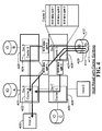
- FIGS. 1 a and 1 b illustrate examples of IO network topologies where IOC to IOC distributed caching can be used.
- HBA/IO bridge-switch ( 100 ) caches IO's A to H ( 101 , 102 , 103 , 104 , 114 , 113 , 110 , and 109 ), depending on the request of the host ( 115 ). It also caches IO's A and B ( 101 and 102 ) for use by other HBA/IO bridges-switches ( 105 , 106 , and 112 ).
- HBA/IO bridge-switch ( 105 ) caches IO's C and D ( 103 and 104 ) for use by other HBA/IO bridges-switches ( 100 , 106 , and 112 ).
- HBA/IO bridge-switch ( 112 ) caches IO's A to H ( 101 , 102 , 103 , 104 , 114 , 113 , 110 , and 109 ), depending on the request of Host ( 111 ). It also caches IO's E and F ( 114 and 113 ) for use by other HBA/IO bridges-switches ( 100 , 105 , and 106 ).
- HBA/IO bridge-switch ( 108 ) caches IO's A to H ( 101 , 102 , 103 , 104 , 114 , 113 , 110 , and 109 ), depending on the request of Host ( 106 ). It also caches IO's G and H ( 110 and 109 ) for use by other HBA/IO bridges-switches ( 100 , 105 , and 112 ).
- FIG. 1 b caching behavior of HBA/IO bridges-switches is the same as those in FIG. 1 a —each HBA/IO bridge-switch caches IO data, both local and remote, as instructed by its connecting host, and caches local IO data for use by the other HBA/IO bridges-switches in the IO network.
- FIG. 1 c shows the internal block diagram of the caching HBA/IO bridge-switch ( 150 ).
- the main elements of the caching HBA/IO bridge-switch ( 150 ) are the one or more CPUs ( 155 ), POWER GUARDTM circuit ( 154 ), solid state memory DMA control ( 156 ), volatile memory DMA control ( 157 ), solid state memory modules ( 152 ), volatile memory modules ( 153 ), IO DMA controllers ( 158 , 159 , and 160 ).
- the IO DMA controllers ( 158 , 159 , and 160 ) interface to their respective external IO devices ( 161 , 162 , and 163 ).
- the external IO devices ( 161 , 162 , and 163 ) can be any on the possible external IO devices ( 167 ), which are: IO storage devices ( 168 ), another caching HBA/IO bridge-switch ( 169 ), or a host ( 170 ).
- the external IO devices interface to the caching HBA/IO bridge-switch can be: (1) PCI, PCI-X, or PCI Express for host, (2) IDE, ATA, SATA, USB, SCSI, etc. for IO devices, (3) Fibre Channel, Ethernet, PCI Express, etc. for other HBA/IO bridge-switch.
- the HBA/IO bridge-switch ( 150 ) cache memory ( 151 ) is composed of the solid state memory modules such as arrays for flash devices, MRAMs, etc. ( 152 ) and volatile memory modules such as arrays of SRAMs, SDRAMs, etc. ( 153 ).
- the contents ( 166 ) of the cache memory ( 151 ) is composed mainly of the cache control information ( 164 ) and the cache data lines ( 165 ) itself.
- FIG. 2 shows how the distributed caching mechanism works during IO reads in an IO network comprising of 2 hosts (host A and host C), 4 IO devices (IO A-IO D), and 4 IO caching switches (Sw A-Sw D).
- host A 212
- the initial read path is shown by the diagonal arrow ( 200 ) and it traverses switch D ( 230 ) and switch A ( 210 ).
- the read data can either be cached in cache D ( 231 ), in cache A ( 211 ), or in both cache A ( 211 ) and cache D ( 231 ), depending on the caching options selected and the cache resources available.
- the requested IO device D data is cached in both cache A ( 211 ) and cache D ( 231 ).
- Switch A ( 210 ) being nearest to host A ( 212 ) than any other IO bridges/switches, can immediately service the IO requests of host A ( 212 ) if there's a cache hit in cache A ( 211 ).
- Cache D ( 231 ) is caching the IO request to IO device D ( 232 ), and any requests to IO device D ( 232 ) can first check the contents of cache D ( 231 ).
- cache A ( 211 ) and cache D ( 231 ) have the data, and host C ( 222 ) requests for the same data, host C ( 222 ) may get the data from either cache A ( 211 ) or cache D ( 231 ) without knowing it, depending on which cache transfer is more optimized.
- switch C ( 220 ) Utilizing standard protocols (like Advanced Switching, Ethernet, etc.), host C ( 222 ) using switch C ( 220 ) sends its request to device D ( 232 ) through switch D ( 230 ) via any of these four paths depending on which is most optimized or has less traffic—switch C ( 220 ) to switch A ( 210 ) to switch D ( 230 ), switch C ( 220 ) to switch B ( 213 ) to switch D ( 230 ), switch C ( 220 ) to switch A ( 210 ) to switch B ( 213 ) to switch D ( 230 ), or switch C ( 220 ) to switch D ( 230 ).
- switch A ( 210 ) may respond to the request since the requested IO data is already in cache A ( 211 ).
- the data path from switch A ( 210 ) to switch C ( 220 ) is shown by the vertical line ( 202 ).
- switch D ( 230 ) has 2 options to send the requested data—either directly from its cache, or instruct switch A ( 210 ) to send the data from its cache on its behalf. These two options are shown by the vertical arrow ( 202 ) traversing switch A ( 210 ) and switch C ( 220 ), and the L-shaped arrow ( 201 ) traversing switch D ( 230 ) and switch C ( 220 ).
- the system has the option to cache the read data in cache C ( 221 ), making the data available in 3 possible location of the system.
- This distributed cache arrangement allows redundancy and much flexibility in optimizing the IO access of the hosts.
- the general goal of this optimization is to cache the data as near to the requesting host as possible.
- Another benefit of this scheme is in case the data is too big for one switch's cache, there is an option of caching the data in the cache of the nearby switches.
- FIG. 3 shows how the distributed caching mechanism works during IO writes in the same IO network as described in FIG. 2 .
- host A ( 312 ) needs to write data to IO device D ( 332 ).
- the initial write path is shown by the diagonal arrow ( 300 ) and it traverses switch A ( 310 ) and switch D ( 330 ).
- the write path ( 300 ) is assumed only for this example and other paths can be selected depending on the options and available resources of the switch A ( 310 ).
- the write data can either be cached in cache A ( 310 ), in cache D ( 330 ), or in both cache A ( 310 ) and cache D ( 330 ), depending on the caching options selected and the resources available.
- the requested IO device D data is cached initially in cache A ( 311 ) and then later in cache D ( 331 ).
- Switch D ( 330 ) has 2 options on sending the requested data to host C ( 322 ) via switch C ( 321 )—(1) Switch D ( 330 ) can give the requested data by reading from cache D ( 331 ) and return it to switch C ( 320 ). This read data path is shown by the L-shaped arrow ( 301 ) traversing switch D ( 330 ) and switch C ( 320 ). (2).
- Switch D ( 330 ) can inform switch C ( 320 ), that the requested data is in both cache A ( 311 ) and cache D ( 331 ).
- Switch C ( 320 ) in this case, now has the option to read from either of the 2 caches via the vertical arrow ( 302 ) traversing switch A ( 310 ) and switch C ( 320 ), and the L-shaped arrow ( 301 ) traversing switch D ( 330 ) and switch C ( 320 ).
- the final chosen path is based on algorithms, and some factors like routing, bandwidth, and cache state considerations.
- switch A ( 310 ) may respond to the request since cache A ( 311 ) contains the requested data.
- other paths can also be selected to pass the request depending on the algorithms, available resources, and other factors affecting the IO switches in the IO network.
- FIG. 4 shows how the caching mechanism works during IO reads with “cache splitting”.
- host A ( 400 ) is requesting data from IO device D ( 412 ) via switch D ( 408 ).
- the requested data can be stored fully in cache A ( 402 )
- caches B ( 404 ) and C ( 405 ) need not be used as cache A ( 402 ) extensions.
- the requested data is much bigger than the allowable size for a single transfer by the protocol of the bridges/switches connections or by the available buffers of the receiving intermediate bridge/switch.
- switch D ( 408 ) can only send the data from IO device D ( 412 ) in multiple chunks due to protocol-specific data size limitation or insufficient available buffers of the receiving (intermediate) bridge/switch.
- switch D ( 408 ) can instead split the requested data and send to switch A ( 401 ) through different paths at the same time. After storing the requested data to cache D ( 407 ), the data is split into 3 parts and each part is sent to cache A ( 402 ) via 3 different paths.
- This distributed cache procedure allows the requested data to be transferred at 3 times faster than normal transaction since the data bandwidth is increased by 3 folds.
- the data bandwidth can further be increased depending on the number of participating HBA/IO bridges-switches in the network.
- FIG. 5 shows how the distributed caching mechanism works during IO reads with “cache migration”. Similar to the scenario in FIG. 4 , this figure illustrates host A ( 500 ) requesting data from a remote IO device, this time to IO device I 2 ( 520 ) via switch I ( 512 ). The difference in this example is that the requested data is assumed to be much bigger than cache A ( 501 ) can hold. In order to speed up the return of the requested data to host A ( 500 ), data can be moved closer to switch A ( 502 ) and distribute the data to other IO bridges/switches. For more optimized operation, caches of the switches near the requesting host switch, switch A ( 502 ), are used.
- the IO bridges/switches nearest switch A ( 502 ) are switches I ( 512 ), G ( 514 ), H ( 515 ), B ( 503 ), E ( 507 ), D ( 505 ), F ( 508 ), and C ( 504 ), and associated caches of these switches are candidates for cache extension. Assuming the requested IO data by the host A ( 500 ) is split into 4 parts as shown in ( 518 ), switch I ( 512 ) will select 3 more caches to distribute the remaining 3 splits. Note that different factors such as available resources, number of hops from the source of IO data and to the target cache, etc.
- caches E ( 506 ), F ( 509 ), and H ( 516 ) are selected as cache A ( 501 ) extensions.
- switch I ( 512 ) starts transferring the requested IO data after fetching from IO device I 2 ( 520 ) and storing to cache I ( 513 ) via the vertical path ( 519 ).
- the splits comprising the whole requested data can be transferred to cache A ( 501 ) and its extensions all at same time. The split and the associated path towards cache A ( 501 ) and its cache extensions are illustrated.
- Cache A ( 501 ) receives split 1 via the diagonal path ( 521 ) which traverses switches I ( 512 ) and A ( 502 ).
- Extension cache F ( 509 ) receives split 2 via the vertical path ( 511 ) which traverses switches I ( 512 ) and F ( 508 ).
- Extension cache E receives split 3 via the diagonal path ( 510 ) that traverses switches I ( 512 ) and E ( 507 ).
- Extension cache H ( 516 ) receives split 4 via the horizontal path ( 517 ) that traverses switches I ( 512 ) and H ( 515 ).
- switch I prior to sending the splits to their target caches, there is a handshaking process between the source switch (switch I) and the participating switches to ensure that the splits can be cached.
- switch I informs switch A ( 502 ) via message that the remaining IO data can be fetched from its nearby switches.
- split data can be requested by switch A ( 502 ) or switches E ( 507 ), F ( 508 ), and H ( 515 ) can be instructed via message by switch I ( 512 ) to send the splits to switch A ( 502 ).
- switch A ( 502 ) If switch A ( 502 ) is to fetch the splits, it will construct read requests of specific splits targeting IO device I 2 ( 520 ) and sends the requests to path that will pass through the switches that contain the split. This way, the intermediate switch that contains the specific split can detect a cache hit on the request and return the requested split instead. For example, knowing that split 2 is stored in cache F ( 509 ), switch A ( 502 ) will construct a read request for split 2 targeting IO device I 2 and will send the request through switch F ( 508 ). Since split 2 is stored in cache F ( 509 ), switch F ( 508 ) will detect that the requested data is in its cache and thus will respond to the request and send the data from its cache. The same process is performed when requesting splits 3 and 4 .
- Switch A ( 502 ) sends requests for split 3 and 4 to IO device I 2 ( 520 ) through switches E ( 507 ) and H ( 515 ) respectively and the switches will return the requested splits from their caches. If switches E ( 507 ), F ( 508 ), and H ( 515 ) are to send the remaining data to switch A ( 502 ) as instructed by switch I ( 512 ), they can send the splits as message payloads.
- This distributed caching technique is a variation of “cache splitting” which is used not only to increase the data transfer speed but also extends the cache by utilizing other HBA/IO bridges-switches caches.
- “Cache migration” is not limited to the scenario discussed above. It can also be used for other cases such as when the source switch's cache itself is insufficient to cache all the requested data thus after fetching some data and transferred to other caches, it replaces the cache content with new IO data. It is also not limited to the number of remote IO caches where data is to be distributed. Depending on the requirement or the application, data can be distributed to as much as all the components in the network.
- IO switches nearest the host switch, switch A ( 502 ), and the selected paths from switch I ( 512 ) to these IO switches are assumptions only and may or may not be the most optimized selection for the sample scenario. Note that available resources, current traffic from one path to another, number of intermediate IO switches to cross until the target is reached, and other factors must be considered when selecting the paths and cache extensions due to latencies and overhead that may be involved when performing the distributed caching operation. This scenario only illustrates how the distributed caching with “cache migration” works and caching algorithms to use must be considered to effectively implement this cache operation.
- FIG. 6 shows how the cache split and sharing mechanism works during IO writes.
- host A 601
- IO device I 2 625
- switch A 603
- the switches nearest to switch A ( 603 ) are switches I ( 618 ), G ( 621 ), H ( 622 ), B ( 606 ), E ( 614 ), D ( 612 ), F ( 615 ), and C ( 607 ).
- the write data can be split and distributed to any or all the nearby switches.
- the write data is split into 4 parts as shown in ( 600 ) and thus only 4 of the nearby switches can be selected. Note that available resources, current traffic to and from the switch, number of hops from the switch to the target, and other factors must be considered when selecting nearby switches as cache extensions for the write data.
- switch A ( 603 ) starts transferring the write data once enough data are fetched from host A ( 601 ). Note that prior to accepting the write data ( 600 ) from host A ( 601 ), switch A ( 603 ) handshakes with the selected switches (switches B ( 606 ), D ( 612 ), and E ( 614 )) by using messages.
- Switches B ( 606 ), D ( 612 ), and E ( 614 ) then allocates space in their respective caches (cache B ( 605 ), D ( 611 ), and E ( 613 )). Once the handshake is done, there is now space in cache A ( 602 ), B ( 605 ), D ( 611 ), and E ( 613 ) to accommodate the write data ( 600 ) as shown in the figure.
- switch A ( 603 ) receives a portion of the write data enough to make a split, switch A ( 603 ) transmits it right-away to one of the selected switches.
- switch A ( 603 ) After receiving split 4 from host A ( 601 ), switch A ( 603 ) sends via a message command (with the split as payload) to switch E ( 614 ) which then stores the split to its cache, cache E ( 613 ).
- the write path to cache E ( 613 ) is shown by the diagonal path that traverses switches A ( 603 ) and E ( 614 ). This procedure continues until all the splits comprising the entire write data are stored to cache A ( 602 ) and all its extensions—caches B ( 605 ), D ( 611 ), and E ( 613 ).
- the paths to the other caches are also shown in the figure.
- Split 2 is written to cache B ( 605 ) via the horizontal path ( 604 ) that traverses switches A ( 603 ) and B ( 606 ).
- Split 3 is written to cache D ( 611 ) via the vertical path ( 608 ) that traverses switches A ( 603 ) and D ( 612 ).
- switches A ( 603 ), B ( 606 ), D ( 612 ), and E ( 614 ) eventually writes the respective split data from their respective caches A ( 602 ), B ( 605 ), D ( 611 ), and E ( 613 ) to the final destination which is IO device I 2 ( 625 ).
- Switch A ( 603 ) can flush the split data in cache A ( 602 ) to IO device I 2 ( 625 ), using the diagonal path ( 624 ) passing through switches A ( 603 and I ( 618 ).
- Switch B ( 606 ) can flush the split data in cache B ( 605 ) to IO device I 2 ( 625 ) using the diagonal path ( 623 ) passing through switches B ( 606 ) and I ( 618 ).
- Switch D ( 612 ) can flush the split data in cache D ( 611 ) to IO device I 2 ( 625 ), using the diagonal path ( 620 ) passing through switch D ( 612 ) and I ( 618 ).
- Switch E ( 614 ) can flush the split data in cache E ( 613 ) to IO device I 2 ( 625 ), using the diagonal path ( 616 ) passing through switches E ( 614 ), and I ( 618 ).
- switch I ( 618 ) handles all the transactions to the IO devices I 2 ( 625 ) and I 1 , and will respond depending on the write command (whether write-through or write-back) of the other switches. If write-through, switch I ( 618 ) will only acknowledge the write command once the write data is written to the IO device. If write-back, switch I ( 618 ) will acknowledge the write command once the write data is written to cache I ( 619 ).
- this split-shared caching technique is used not only to increase the data transfer speed but also extends the cache by utilizing other HBA/IO bridges-switches caches.
- “Cache split-sharing” is not limited to the scenario discussed above. It can also be used for other cases such as when the IO device switch's cache stores the entire write data before splitting and then distributing to nearby switches, cache is used as temporary buffer only for a split thus the actual write data are distributed only to the nearby switches excluding the IO switch connected to the host, or any other possible cases. Note that depending on the requirement or the application, data can be distributed to as much as all the components in the network.
- IO switches nearest the host switch, switch A ( 603 ), and the selected paths to switch I ( 618 ) from these IO switches are assumptions only and may or may not be the most optimized selection for the sample scenario. Note that available resources, current traffic from one path to another, number of intermediate IO switches to cross until the target is reached, and other factors must be considered when selecting the paths and cache extensions due to latencies and overhead that may be involved when performing the distributed caching operation. This scenario only illustrates how the distributed caching with “cache split-sharing” works and caching algorithms to use must be considered to effectively implement this cache operation.
- FIG. 7 shows the flushing of cache content by an IO bridge/switch. Assuming based on a flushing algorithm that is running in switch B ( 702 ), some contents of cache B ( 703 ) are needed to be flushed. Depending on the cache content to be flushed, flushing can be to local IO device(s) or to remote IO device(s). For this scenario, it is assumed that the contents to be flushed are a portion of IO device B ( 701 ) and a portion of IO device C ( 707 ). To flush cache content to IO device B ( 701 ), switch B ( 702 ) performs a write transaction with the IO device with the cache content to flush as the write data.
- the process of writing the cache content to its location in the IO device is specific to the protocol being supported by the switch and the IO device.
- switch B To flush cache content to IO device C ( 707 ), switch B ( 702 ) performs a write transaction with switch C ( 709 ) with the cache content to be flushed as the write data.
- flush data can pass through either of the 3 possible paths—(1) the diagonal path ( 704 ) from switch B ( 702 ) to switch C ( 709 ), (2) the rotated L-shaped path ( 705 ) that traverses switches B ( 702 ), A ( 700 ), and C ( 709 ), and (3) the flipped L-shaped path ( 706 ) that traverses switches B ( 702 ), D ( 710 ), and C ( 709 ).
- flush data can also be split and send to any or all the 3 paths.
- switch C ( 709 ) handles all the transactions to IO device C ( 707 ) and thus for the case of flushing to IO device C ( 707 ), a switch needs only to make sure that the flush data is received by switch C ( 709 ) and not whether the flush data is successfully written to the IO device C ( 707 ) or not.
- switch C ( 709 ) may first cache the flush data received from other switches or write directly to the IO device C ( 707 ) before acknowledging the flush/write command by other switches.
- flushing method described is not limited to the IO network illustrated in FIG. 7 .
- the flushing method can also be applied to the IO network in FIG. 6 and other architectures which utilizes the distributed caching invention.
- FIG. 8 shows the flow chart for the typical host read.
- the host sends a read IO request which is then received by the HBA via its interface with the host ( 801 ) and stores to its command buffer.
- the CPU of the HBA retrieves the host command, interprets it, and determines the target ( 802 ) IO device(s). If it is determined that the host command is accessing an IO device directly connected to the HBA ( 803 ), the HBA performs a read operation to its local IO device as discussed in FIG. 17 of the above-discussed previous patent ( 805 )—“hybrid storage device”.
- the CPU first check if the requested IO data is locally cached ( 804 ), before it translates and forwards the command through the network. If a cache hit occurs ( 806 ), the HBA responds to the host command and sends the data from its cache ( 814 ). If no cache hit, the CPU allocates a space in cache for the requested data. Before it can allocate a cache space, the CPU first checks if there's a free space in its cache ( 807 ). If the cache is full ( 808 ), the CPU either invalidates some cache contents or flush to the appropriate destination ( 809 ). After freeing some cache space, the CPU then creates control information for the allocated cache space ( 810 ).
- the CPU then translates the host command into one that is understandable by the network components and sends it through the network ( 811 ).
- the network then routes the sent command to its target ( 812 ).
- the HBA can perform other operation or wait for the response to the command.
- the HBA receives the requested data from the network ( 816 ) via its IO interface controller and stores to the previously allocated space in cache. Once all or a significant amount of the requested data are cached, the HBA starts to transfer the data to the host ( 814 ).
- the HBA depending on the network protocol, may receive a completion or status information on the data transferred from the network.
- This received completion may be used by the HBA to generate another version of it once it is done transferring the requested data to the host ( 815 ).
- the sending of completion or status information by the HBA to host is optional and depends on the protocol being implemented by the host and the HBA. After sending all the data to host, or after sending the completion, the CPU updates its local cache of information on the requested data ( 818 ).
- FIG. 9 shows the flow chart for the typical host write.
- the host sends a write IO request which is then received by the HBA via its interface with the host ( 901 ) and stores to its command buffer.
- the CPU of the HBA retrieves the host command, interprets it, and determines the target ( 902 ) IO device. If it is determined that the host command is accessing an IO device directly connected to the HBA ( 903 ), the HBA performs a write operation to its local IO device as discussed in FIG. 18 of the previous patent ( 904 )—“hybrid storage device”.
- the CPU first check if the requested IO write data is locally cached ( 913 ), before it translates and forwards the command through the network. If a cache hit occurs ( 914 ), the HBA responds to the host command and sends a protocol-specific write-acknowledge (optional) or a similar handshake signifying its readiness to accept the write data ( 910 ). If no local cache hit occurs, the CPU checks if the requested data is cached in the network system ( 915 ). If the requested data is cached in the network, the CPU handshakes to synchronize their cache control information and to inform the share-cache switches that an incoming write command will write to their cached data ( 916 ).
- the CPU prepares for the split write command, by checking the cache and routing control information ( 917 ). After the split commands has been determined by the CPU, it updates its cache control information, and prepares the cache for the incoming write data ( 909 ). Then, the HBA responds to the host command and sends a protocol-specific write-acknowledge (optional) or a similar handshake signifying its readiness to accept the write data ( 910 ). If no cache hit occurs for the entire network of distributed cache, the CPU allocates a space in cache for the requested data. Before it can allocate a cache space, the CPU first checks if there's a free space in its cache ( 905 ).
- cache space If there is available cache space ( 906 ), it updates its cache control information, and prepares the cache for the incoming write data ( 909 ). Then, the HBA responds to the host command and sends a protocol-specific write-acknowledge (optional) or a similar handshake signifying its readiness to accept the write data ( 910 ). If the cache is full, the CPU either invalidates some cache contents or flushes to the appropriate destination ( 907 ). If the freed cache space is enough for the requested data ( 908 ), the CPU updates its cache control information, and prepares the cache for the incoming write data ( 909 ).
- the HBA responds to the host command and sends a protocol-specific write-acknowledge (optional) or a similar handshake signifying its readiness to accept the write data ( 910 ). If the freed cache space is too small for the requested data, the CPU requests for additional cache allocation sharing to nearby switches, and handshakes to synchronize their cache control information and to inform the share-cache switches that an incoming write command will write to their cached data ( 916 ). Once the handshake is done, the CPU prepares for the split write command, by checking the cache and routing control information ( 917 ). After the split commands has been determined by the CPU, it updates its cache control information, and prepares the cache for the incoming write data ( 909 ).
- the HBA responds to the host command and sends a protocol-specific write-acknowledge (optional) or a similar handshake signifying its readiness to accept the write data ( 910 ).
- the CPU signifies readiness to accept the write data ( 910 )
- the CPU starts to receive the write data from the host ( 918 ).
- the CPU translates the host command and data into one that is understandable by the network components and does the write command sequence with the affected network components ( 920 ). This is done when there is a need to transmit the write data to the system (e.g. received a write through command from the host, or need for cache sharing).
- the CPU may optionally send completion status to the host ( 919 ).
- the completion status maybe auto-generated by the CPU, or it may be the translated completion status that was received from the network components.
- the CPU waits for all the respective completion status of the network components, before sending the translated completion status to the host.
- the sending of completion or status information by the HBA to host is optional and depends on the protocol being implemented by the host and the HBA. After transferring all the write data from the host, or after sending the completion status, the CPU updates its local cache control information and synchronizes its cache with the other switches if needed ( 912 ).
- FIG. 10 shows the flow chart of how a network switch processes a received frame from the network.
- a frame is received by an IO switch via its IO interface controller.
- the initial checking is determining if the received frame is targeting the IO switch (or the IO device(s) connected to it). If it is determined that the frame is not for the IO switch ( 1001 ), the CPU of the IO switch checks if the frame is targeting a locally-cached space ( 1002 ) instead. If no cache hit, the frame is routed back to the network by the IO switch.
- the CPU of the IO switch identifies whether the frame is a command, data, status information, or a message ( 1004 ). If the frame is determined to be a command ( 1006 ), the type of the command is determined ( 1013 ), and the frame is process accordingly. The process proceeds to ( 1012 ) if the frame is identified as a write command; else (if the command is a read command) the process proceeds to ( 1014 ). If the received frames is determined to be not a command, the CPU checks if it is a message ( 1008 ) or an IO write data ( 1010 ). If the frame is a message, the process proceeds to ( 1009 ). If the frame is a write data, the process proceeds to ( 1012 ). If the frame is determined to be neither a command, message, nor write data, then an error is detected by the IO switch ( 1011 ).
- FIG. 11 shows the flow chart of how a network switch processes a received read command from the network.
- the switch's CPU determines the target of the read command ( 1101 )—whether the IO devices connected directly to the switch (yes) or IO devices connected to other switches (no). If the CPU has determined that the read command is accessing locally connected IO devices, it performs read transaction with the IO devices as discussed in FIG. 17 of the previous patent ( 1102 )—“hybrid storage device”. If the read command is determined to be accessing remote IO devices, the CPU first check if the target space is already cached ( 1103 ), before it concludes that an error is detected ( 1106 ).
- the IO switch starts sending the data to the requestor through the network ( 1105 ).
- the process of how the read data is sent is implementation-specific but follows the protocol being implemented by the network. After sending all the data, the IO switch may send a completion or status information to the requestor, depending on the network protocol ( 1107 ).
- FIG. 12 shows the flow chart of how read data is sent by the target IO switch to the requestor.
- the IO switch's CPU determines the type of operation of how the read data will be sent.
- the read data is fetched from the cache and sent to the network ( 1207 ). Depending on the maximum allowable data size per transfer of the network, the read data may be chunked before sending to the requestor. If there are more data to be sent ( 1210 ), the remaining data are fetched from the cache and sent through the network. This procedure continues until all the read data are transferred to the requestor.
- Case (2) is the process of splitting the read data before sending to the requestor. Unlike case (1) which uses a single path to the requestor when sending the read data, this case utilizes multiple paths, and thus increasing the speed and size of the data transfer.
- the IO switch Before the IO switch sends the read data, it first divides the data into splits ( 1202 ). The maximum number of splits is implementation-specific and the size of each split can be as large as the maximum allowable data transfer size by the network protocol. The maximum number of paths to use when sending the splits is also implementation-specific. After determining the number of splits, the IO switch checks from a routing table for different paths to the requestor and selects the optimized paths ( 1205 ).
- the IO switch starts sending the read data, in the form of splits, to the requestor using the selected paths. If there are more data to send ( 1211 ), the splits are fetched from the cache and sent through the paths. This procedure continues until all the read data are sent to the requestor.
- Case (3) termed as cache migration, is typically the same as case (2) except that the targets of the splits are the IO switches near the requestor.
- the IO switch determines the other IO switches near the requestor ( 1204 ). Once determined, the IO switch checks from a routing table the paths to these neighbors ( 1206 ) and sends the read data, in splits, to these neighbors via the selected paths. The IO switch continues to fetch the read data from cache until all are transmitted to the requestor's neighbors. Once all data are transmitted, the IO switch creates a message ( 1215 ) informing the requestor of the location of the split read data where the requestor can fetch eventually.
- FIG. 13 shows the flow chart for the processing of write command by the host switch.
- HBA Prior to distributed writes, HBA has already allocated space in remote IO bridge(s)/switch(es) cache(s) through messaging. The messaging indicates the details on the Write Data to be cached such as LBA, DEVID, etc.
- remote IO bridge(s)/switch(es) can already determine whether write data is to be cached or not whenever one (write data) passes through. There are 4 cases for this write command:
- the write data needs only the local HBA cache, and the host command requires write through.
- the CPU checks if the write data needs the network distributed shared cache ( 1300 ). If not, the CPU checks if the command requires write back ( 1301 ). If not, command requires write through and the CPU translates the command and sends the command to the IO switch which has the target IO device ( 1302 ). In ( 1303 ) the CPU receives (an optional) write acknowledge, or some handshake from the IO switch (that has the target IO device) that the target IO device is ready to receive the write data. After this, the CPU proceeds with transferring the write data to the target IO device ( 1304 ). After the write data has been transferred to the device (depending on the protocol) the HBA optionally receives completion status information from the target IO device ( 1305 ). For this case, the HBA switch needs to talk only directly with the IO switch.
- Case (2) the write data needs only the local HBA cache, and the host command requires write back.
- the CPU checks if the write data needs the network distributed shared cache ( 1300 ). If not, the CPU checks if the command requires write back ( 1301 ). If yes, the HBA switch already has the write data in it's cache, and it optionally generates completion status for the host (depending on the protocol) ( 1306 ). For this case, the HBA switch does need to talk with any other switch in the network immediately.
- the write data needs the distributed shared cache, and the host command requires write back.
- the CPU checks if the write data needs the network distributed shared cache ( 1300 ). If yes, the CPU translates and splits the write command to be transmitted to the remote switches with shared cache ( 1307 ). Then the CPU checks if the command requires write back ( 1308 ). If yes, the CPU sends the split commands to the remote switches which have the shared cache ( 1309 ). In ( 1310 ) the CPU receives (an optional) write acknowledge, or some handshake from the remote switches that they are ready to receive the write data. After this, the CPU proceeds with transferring the write data to the remote switches ( 1311 ). After the write data has been transferred (depending on the protocol), the HBA optionally waits for all the completion status information from the remote switches ( 1312 ). For this case, the HBA switch needs to talk only directly with the remote switches.
- the write data needs the distributed shared cache, and the host command requires write through.
- the CPU checks if the write data needs the network distributed shared cache ( 1300 ). If yes, the CPU translates and splits the write command to be transmitted to the remote switches with shared cache ( 1307 ). Then the CPU checks if the command requires write back ( 1308 ). If no, write through is required and the CPU sends the split commands to the remote switches which have the shared cache, and to the IO switch (so the HBA switch can write through the target device its share of the split cache) ( 1313 ). In ( 1314 ) the CPU receives (an optional) write acknowledge, or some handshake from the remote and IO switches that they are ready to receive the write data.
- the CPU proceeds with transferring the write data to the remote and IO switches ( 1315 ).
- the HBA optionally waits for all the completion status information from the remote and IO switches ( 1316 ). For this case, the HBA switch needs to talk directly with the remote and IO switches.
- FIG. 14 shows the flow chart for the processing of write command by an intermediate/target IO switch.
- the process starts in ( 1400 ) after the CPU determines that there is a write command for the switch itself.
- the CPU first checks if the data already has an allocated share cache (which was borrowed by the other switches) which was pre-allocated in a previous cache sharing messaging scheme. ( 1401 ). If yes, the CPU proceeds to send an optional write acknowledge ( 1402 ), or a handshake signifying readiness to accept the write data. If no, the CPU checks if the data is accessing local IO data that's already cached ( 1408 ).). If yes, the CPU proceeds to send an optional write acknowledge ( 1402 ), or a handshake signifying readiness to accept the write data.
- the CPU checks if there are enough free cache space for the write data ( 1411 ). If there is available cache space ( 1412 ), the CPU updates the cache control information ( 1414 ), and proceeds to send an optional write acknowledge ( 1402 ), or a handshake signifying readiness to accept the write data. If there is no more free cache space, the CPU flushes some cache contents to free up cache space ( 1413 ), and then updates the cache control information ( 1414 ), and proceeds to send an optional write acknowledge ( 1402 ), or a handshake signifying readiness to accept the write data. In ( 1403 ), the CPU receives the write data. The CPU then sees the target of the write data ( 1404 ).
- the process then goes to the write process for the local IO device ( 1409 ) (refer to FIG. 18 or conventional art).
- the CPU checks if the command is a write back ( 1406 ). If yes, (depending on the protocol), the CPU optionally sends the completion status ( 1407 ). If no, the CPU performs the write process to the IO switch, where the target IO device is attached ( 1410 ), before (depending on the protocol) the CPU optionally sends the completion status ( 1407 ).
- FIG. 15 shows the flow chart for the processing of message by an IO switch.
- the IO switch determines the type of the message received. If it is identified that the message is not cache-related ( 1501 ), the process proceeds to ( 1502 ) processing of message according to type which is implementation-specific. If the message is cache-related, the IO switch CPU checks if it as an accompanying data payload ( 1503 ). Depending on the field values of the message, the associated payload can be the data to be cached by the IO switch. If it is determined that the cache message has a payload, the CPU checks if it is previously cached in the IO switch ( 1506 ).
- the message payload replaces the one in the cache and the CPU updates the corresponding mapping ( 1515 ). If there is no cache hit, meaning the message is not yet cached, new cache information is created for the message payload ( 1510 ) before it is stored in the cache. After storing the message payload to cache, the CPU updates the corresponding map ( 1515 ). Note that prior to ( 1510 ), the IO switch that sent the cache message with payload has already communicated with the IO switch to ensure that the message payload can be received and stored to cache.
- the IO switch CPU processes and determines the type of the message ( 1505 ). In the embodiment of this invention, there are defined message without payload types—(1) invalidate cache, (2) cache migrated, and (3) allocate cache. In ( 1507 ), it is checked if the message relates to allocation of cache space. If the message is determined to be cache allocation-related, it is further checked if it is a cache request or response ( 1508 ). If cache allocation request, the IO switch CPU allocates some cache space ( 1512 ).
- Allocation of cache space includes flushing or invalidating of some cache contents to be able to make space for the incoming data to be cached, in case the cache is full or the cache space being requested by the message is larger than the current free space.
- the CPU may create a respond message indicating if the space is successfully allocated or not and send to the originator of the message request. If the cache allocate message is a completion or a response to a previous request, the IO switch CPU processes the message ( 1509 ) and determines whether it has successfully allocated a space to another IO switch cache. If it has allocated a cache, the IO switch can start sending the data to the remote cache.
- the IO switch CPU also has the option not to use the allocated remote cache space if the returned message response indicates a much smaller space than it has requested, or if it has already transferred the data to a different IO switch cache. It is assumed that after allocating a cache space for another IO switch, the local CPU also allocates a limited time frame for the remote IO switch to use the allocated cache space. If the time frame has expired, the allocated cache space is invalidated and can be used by the IO switch itself to cache local IO or by a different IO switch as its extended cache.
- FIG. 16 shows the flow chart for flushing of cache by an IO switch. This flow chart discusses the details of the illustration in FIG. 7 .
- Cache flushing can be performed on the background, during messaging, during reads, or during writes.
- the IO switch CPU checks the local cache if some contents are needed to be flushed. This instance can be activated during idle periods ( 1600 ) or when the IO switch CPU is processing a message related to cache allocation ( 1602 ).
- Checking of cache content includes counting of free entries in the cache table if the current number of inputs has reached the limit ( 1603 ). If the limit hasn't been reached yet, then there would be no need of cache flushing.
- the IO switch CPU determines based on an algorithm, the cache table entries that need to be flushed ( 1604 ). This instance can be activated during read ( 1605 ) or write operation ( 1606 ). After getting the table entries to be flushed, the IO switch CPU determines the location where to flush the selected entries ( 1607 ). In ( 1608 ), it is determined whether the location is local or remote to the IO switch. If the cache content is to be flushed to the local IO device/s, the IO switch performs flushing of cache content as discussed in FIG. 19 of the above noted conventional patent ( 1609 )—“hybrid storage device”.
- the IO switch simply performs normal write transaction with the IO switches to which the cache content is/are to be flushed ( 1611 ) with the cache content to be flushed as the write data. After flushing the cache data to the corresponding location, the IO switch CPU has the option to check for remote copies of the recently flushed data ( 1610 ). If remote copies exist, the IO switch CPU may create message/s to invalidate the remote copies and send to the IO switches which have copies of the local IO. Upon receiving the message, remote IO switch has the option to invalidate the affected cache data or update its copy by fetching the latest data from the originator of the invalidate cache message.
- FIG. 17 shows the basic tables used by HBA and IO bridges/switches to perform distributed caching.
- the Generic Switch Cache Remap Table ( 1700 ) controls cache information for the cache.
- the cache may consist of volatile memories like SRAM and SDRAM (level I), non-volatile memories like Flash and MRAM (level II), and rotating hard disks (level III).
- the table has control entries that are located using the LBA Set Index ( 1701 ).
- the Physical Block Address ( 1702 ) has the memory address of the cache or the logical address if the cache consists of rotating hard drives.
- the Location entry ( 1703 ) identifies the particular networked target IO that's being cached and has the Device ID and the LBA of the data.
- the cache state ( 1705 ) has the basic cache information indicating if the cache is invalid, clean, dirty, etc. . . . .
- the Remote Copies ( 1706 ) identifies which other bridges/switch in the system has cached the same data.
- the Remote Copies ( 1706 ) entries may consist of a basic bit map ( 1707 ), with each bit corresponding to a particular bridge/switch Device ID.
- the information in the Generic Switch Cache Remap Table tells the bridge/switch which data in the system is in its cache and it also indicates where the other copies of the cached data are in the system.
- the Local IOC Usage Table ( 1710 ) identifies which bridge/switch in the system is currently caching (or using) the data from the IO device that is locally attached to a particular bridge/switch. This table is found in every bridge/switch that is managing a local IO device that is attached to it. The basic entries for this table are the location ( 1709 ) of the attached local IO device and the Remote Usage Mapping ( 1711 ) of the bridges/switches that are currently caching the attached local IO device. The Location ( 1709 ) entries have the Device ID and the LBA of the data in the locally attached IO device.
- the Remote Usage Mapping ( 1711 ) entries may consist of a basic bit map ( 1708 ), with each bit corresponding to a particular bridge/switch Device ID.
- Data entries in the Local IOC Usage Table ( 1710 ) are not necessarily cached locally in the bridge/switch, and may not be found in the corresponding local Generic Switch Cache Remap Table ( 1700 ).
Abstract
Description
Claims (20)
Priority Applications (1)
| Application Number | Priority Date | Filing Date | Title |
|---|---|---|---|
| US14/216,937 US9720603B1 (en) | 2013-03-15 | 2014-03-17 | IOC to IOC distributed caching architecture |
Applications Claiming Priority (2)
| Application Number | Priority Date | Filing Date | Title |
|---|---|---|---|
| US201361799362P | 2013-03-15 | 2013-03-15 | |
| US14/216,937 US9720603B1 (en) | 2013-03-15 | 2014-03-17 | IOC to IOC distributed caching architecture |
Publications (1)
| Publication Number | Publication Date |
|---|---|
| US9720603B1 true US9720603B1 (en) | 2017-08-01 |
Family
ID=59383282
Family Applications (1)
| Application Number | Title | Priority Date | Filing Date |
|---|---|---|---|
| US14/216,937 Expired - Fee Related US9720603B1 (en) | 2013-03-15 | 2014-03-17 | IOC to IOC distributed caching architecture |
Country Status (1)
| Country | Link |
|---|---|
| US (1) | US9720603B1 (en) |
Cited By (4)
| Publication number | Priority date | Publication date | Assignee | Title |
|---|---|---|---|---|
| US20200089609A1 (en) * | 2018-09-19 | 2020-03-19 | Seagate Technology Llc | Data storage system with write back cache |
| CN112882658A (en) * | 2021-02-10 | 2021-06-01 | 深圳市云网万店科技有限公司 | Data cache capacity expansion method and device, computer equipment and storage medium |
| US11030100B1 (en) | 2019-11-18 | 2021-06-08 | International Business Machines Corporation | Expansion of HBA write cache using NVDIMM |
| EP3839749A4 (en) * | 2018-09-13 | 2021-11-03 | Huawei Technologies Co., Ltd. | Data storage method, device and server |
Citations (268)
| Publication number | Priority date | Publication date | Assignee | Title |
|---|---|---|---|---|
| US4752871A (en) | 1985-09-30 | 1988-06-21 | Motorola, Inc. | Single-chip microcomputer having a program register for controlling two EEPROM arrays |
| US5111058A (en) | 1990-05-23 | 1992-05-05 | Martin Richard A | Circuit for sustaining power supply output following momentary interruption of commercial a.c. power |
| USRE34100E (en) | 1987-01-12 | 1992-10-13 | Seagate Technology, Inc. | Data error correction system |
| US5222046A (en) | 1988-02-17 | 1993-06-22 | Intel Corporation | Processor controlled command port architecture for flash memory |
| WO1994006210A1 (en) | 1992-08-28 | 1994-03-17 | Prabhakar Goel | Multichip ic design using tdm |
| US5297148A (en) | 1989-04-13 | 1994-03-22 | Sundisk Corporation | Flash eeprom system |
| US5341339A (en) | 1992-10-30 | 1994-08-23 | Intel Corporation | Method for wear leveling in a flash EEPROM memory |
| US5371709A (en) | 1993-04-01 | 1994-12-06 | Microchip Technology Incorporated | Power management system for serial EEPROM device |
| US5379401A (en) | 1992-03-31 | 1995-01-03 | Intel Corporation | Flash memory card including circuitry for selectively providing masked and unmasked ready/busy output signals |
| US5388083A (en) | 1993-03-26 | 1995-02-07 | Cirrus Logic, Inc. | Flash memory mass storage architecture |
| US5396468A (en) | 1991-03-15 | 1995-03-07 | Sundisk Corporation | Streamlined write operation for EEPROM system |
| US5406529A (en) | 1992-09-22 | 1995-04-11 | International Business Machines Corporation | Flash non-volatile memory |
| US5432748A (en) | 1992-11-13 | 1995-07-11 | Silicon Storager Technology, Inc. | Solid state peripheral storage device |
| US5448577A (en) | 1992-10-30 | 1995-09-05 | Intel Corporation | Method for reliably storing non-data fields in a flash EEPROM memory array |
| US5459850A (en) | 1993-02-19 | 1995-10-17 | Conner Peripherals, Inc. | Flash solid state drive that emulates a disk drive and stores variable length and fixed lenth data blocks |
| US5479638A (en) | 1993-03-26 | 1995-12-26 | Cirrus Logic, Inc. | Flash memory mass storage architecture incorporation wear leveling technique |
| US5485595A (en) | 1993-03-26 | 1996-01-16 | Cirrus Logic, Inc. | Flash memory mass storage architecture incorporating wear leveling technique without using cam cells |
| US5488711A (en) | 1993-04-01 | 1996-01-30 | Microchip Technology Incorporated | Serial EEPROM device and associated method for reducing data load time using a page mode write cache |
| US5509134A (en) | 1993-06-30 | 1996-04-16 | Intel Corporation | Method and apparatus for execution of operations in a flash memory array |
| US5513138A (en) | 1993-05-13 | 1996-04-30 | Ricoh Co., Ltd. | Memory card having a plurality of EEPROM chips |
| US5524231A (en) | 1993-06-30 | 1996-06-04 | Intel Corporation | Nonvolatile memory card with an address table and an address translation logic for mapping out defective blocks within the memory card |
| US5530828A (en) | 1992-06-22 | 1996-06-25 | Hitachi, Ltd. | Semiconductor storage device including a controller for continuously writing data to and erasing data from a plurality of flash memories |
| US5535328A (en) | 1989-04-13 | 1996-07-09 | Sandisk Corporation | Non-volatile memory system card with flash erasable sectors of EEprom cells including a mechanism for substituting defective cells |
| US5535356A (en) | 1991-09-09 | 1996-07-09 | Samsung Electronics Co., Ltd. | Digital data recording/playback system utilizing EEPROM and ROM memories as a storage medium |
| US5542082A (en) | 1990-12-06 | 1996-07-30 | Tandberg Data A/S | Data storage system connected to a host computer system and having removable data storage media and equipped to read a control program from the removable media into storage employing ID comparison scheme |
| US5542042A (en) | 1993-05-27 | 1996-07-30 | Whirlpool Corporation | Method and apparatus for monitoring volatile memory validity |
| US5548741A (en) | 1991-02-07 | 1996-08-20 | Fuji Photo Film Co., Ltd. | IC memory card system having a host processor selectively operable with an IC memory card including either an SRAM or an EEPROM |
| US5559956A (en) | 1992-01-10 | 1996-09-24 | Kabushiki Kaisha Toshiba | Storage system with a flash memory module |
| US5568423A (en) | 1995-04-14 | 1996-10-22 | Unisys Corporation | Flash memory wear leveling system providing immediate direct access to microprocessor |
| US5568439A (en) | 1988-06-08 | 1996-10-22 | Harari; Eliyahou | Flash EEPROM system which maintains individual memory block cycle counts |
| US5572466A (en) | 1992-10-06 | 1996-11-05 | Kabushiki Kaisha Toshiba | Flash memory chips |
| US5594883A (en) | 1993-04-14 | 1997-01-14 | International Business Machines Corporation | Hierarchical data storage system employing contemporaneous transfer of designated data pages to long write and short read cycle memory |
| US5603001A (en) | 1994-05-09 | 1997-02-11 | Kabushiki Kaisha Toshiba | Semiconductor disk system having a plurality of flash memories |
| US5606532A (en) | 1995-03-17 | 1997-02-25 | Atmel Corporation | EEPROM array with flash-like core |
| US5606529A (en) | 1994-12-20 | 1997-02-25 | Hitachi, Ltd. | Semiconductor disk storage |
| US5619470A (en) | 1994-08-17 | 1997-04-08 | Sharp Kabushiki Kaisha | Non-volatile dynamic random access memory |
| US5627783A (en) | 1995-01-31 | 1997-05-06 | Mitsubishi Denki Kabushiki Kaisha | Semiconductor disk device |
| US5640349A (en) | 1994-08-31 | 1997-06-17 | Tdk Corporation | Flash memory system |
| US5644784A (en) | 1995-03-03 | 1997-07-01 | Intel Corporation | Linear list based DMA control structure |
| US5682509A (en) | 1995-12-13 | 1997-10-28 | Ast Research, Inc. | Bus interface to a RAID architecture |
| US5737742A (en) | 1994-06-29 | 1998-04-07 | Hitachi, Ltd. | Memory system using flash memory and method of controlling the memory system |
| US5787466A (en) | 1996-05-01 | 1998-07-28 | Sun Microsystems, Inc. | Multi-tier cache and method for implementing such a system |
| US5796182A (en) | 1996-06-27 | 1998-08-18 | Martin; Richard A. | Capacator storage circuit for sustaining a DC converter |
| US5799200A (en) | 1995-09-28 | 1998-08-25 | Emc Corporation | Power failure responsive apparatus and method having a shadow dram, a flash ROM, an auxiliary battery, and a controller |
| US5802554A (en) | 1995-02-28 | 1998-09-01 | Panasonic Technologies Inc. | Method and system for reducing memory access latency by providing fine grain direct access to flash memory concurrent with a block transfer therefrom |
| WO1998038568A1 (en) | 1997-02-27 | 1998-09-03 | International Business Machines Corporation | Transformational raid for hierarchical storage management system |
| US5819307A (en) | 1994-10-20 | 1998-10-06 | Fujitsu Limited | Control method in which frequency of data erasures is limited |
| US5822251A (en) | 1997-08-25 | 1998-10-13 | Bit Microsystems, Inc. | Expandable flash-memory mass-storage using shared buddy lines and intermediate flash-bus between device-specific buffers and flash-intelligent DMA controllers |
| US5875351A (en) | 1995-12-11 | 1999-02-23 | Compaq Computer Corporation | System for requesting access to DMA channel having address not in DMA registers by replacing address of DMA register with address of requested DMA channel |
| US5881264A (en) | 1996-01-31 | 1999-03-09 | Kabushiki Kaisha Toshiba | Memory controller and memory control system |
| US5913215A (en) | 1996-04-09 | 1999-06-15 | Seymour I. Rubinstein | Browse by prompted keyword phrases with an improved method for obtaining an initial document set |
| US5918033A (en) | 1997-01-08 | 1999-06-29 | Intel Corporation | Method and apparatus for dynamic location and control of processor resources to increase resolution of data dependency stalls |
| US5930481A (en) | 1995-12-11 | 1999-07-27 | International Business Machines Corporation | System for concurrent cache data access by maintaining and selectively merging multiple ranked part copies |
| US5933849A (en) | 1997-04-10 | 1999-08-03 | At&T Corp | Scalable distributed caching system and method |
| US5943421A (en) | 1995-09-11 | 1999-08-24 | Norand Corporation | Processor having compression and encryption circuitry |
| US5956743A (en) | 1997-08-25 | 1999-09-21 | Bit Microsystems, Inc. | Transparent management at host interface of flash-memory overhead-bytes using flash-specific DMA having programmable processor-interrupt of high-level operations |
| US6000006A (en) | 1997-08-25 | 1999-12-07 | Bit Microsystems, Inc. | Unified re-map and cache-index table with dual write-counters for wear-leveling of non-volatile flash RAM mass storage |
| US6014709A (en) * | 1997-11-05 | 2000-01-11 | Unisys Corporation | Message flow protocol for avoiding deadlocks |
| US6076137A (en) | 1997-12-11 | 2000-06-13 | Lexar Media, Inc. | Method and apparatus for storing location identification information within non-volatile memory devices |
| US6098119A (en) | 1998-01-21 | 2000-08-01 | Mylex Corporation | Apparatus and method that automatically scans for and configures previously non-configured disk drives in accordance with a particular raid level based on the needed raid level |
| US6128303A (en) | 1996-05-09 | 2000-10-03 | Maker Communications, Inc. | Asynchronous transfer mode cell processing system with scoreboard scheduling |
| US6151641A (en) | 1997-09-30 | 2000-11-21 | Lsi Logic Corporation | DMA controller of a RAID storage controller with integrated XOR parity computation capability adapted to compute parity in parallel with the transfer of data segments |
| US6215875B1 (en) | 1997-01-21 | 2001-04-10 | Sony Corporation | Cipher processing system |
| US6230269B1 (en) | 1998-03-04 | 2001-05-08 | Microsoft Corporation | Distributed authentication system and method |
| US20010010066A1 (en) | 1998-07-08 | 2001-07-26 | Chin Kenneth T. | Computer system with adaptive memory arbitration scheme |
| US6298071B1 (en) | 1998-09-03 | 2001-10-02 | Diva Systems Corporation | Method and apparatus for processing variable bit rate information in an information distribution system |
| US6363444B1 (en) | 1999-07-15 | 2002-03-26 | 3Com Corporation | Slave processor to slave memory data transfer with master processor writing address to slave memory and providing control input to slave processor and slave memory |
| US6363441B1 (en) | 1999-03-05 | 2002-03-26 | Silicon Graphics, Inc. | Timing controller having dependency memory, selection serialization component and reordering component for maintaining time dependencies in conversions between sequential and parallel operations using staging memory |
| US20020044486A1 (en) | 2000-10-16 | 2002-04-18 | Cheng-Sheng Chan | IC card with different page sizes to increase endurance |
| US6397267B1 (en) * | 1999-03-04 | 2002-05-28 | Sun Microsystems, Inc. | Redirected I/O for scalable performance storage architecture |
| US6404772B1 (en) | 2000-07-27 | 2002-06-11 | Symbol Technologies, Inc. | Voice and data wireless communications network and method |
| US20020073324A1 (en) | 2000-12-07 | 2002-06-13 | Sony Corporation | System and method for efficiently performing a data encryption operation |
| US20020083262A1 (en) | 1999-04-05 | 2002-06-27 | Tomoya Fukuzumi | Memory device operable with a small-capacity buffer memory and having a flash memory |
| US20020083264A1 (en) | 2000-12-26 | 2002-06-27 | Coulson Richard L. | Hybrid mass storage system and method |
| US20020141244A1 (en) | 2000-11-30 | 2002-10-03 | Bruce Ricardo H. | Parallel erase operations in memory systems |
| US6496939B2 (en) | 1999-09-21 | 2002-12-17 | Bit Microsystems, Inc. | Method and system for controlling data in a computer system in the event of a power failure |
| US20030023817A1 (en) * | 2001-07-27 | 2003-01-30 | Rowlands Joseph B. | Read exclusive for fast, simple invalidate |
| US6526506B1 (en) | 1999-02-25 | 2003-02-25 | Telxon Corporation | Multi-level encryption access point for wireless network |
| US20030065836A1 (en) | 2001-09-28 | 2003-04-03 | Pecone Victor Key | Controller data sharing using a modular DMA architecture |
| US6557095B1 (en) | 1999-12-27 | 2003-04-29 | Intel Corporation | Scheduling operations using a dependency matrix |
| US20030120864A1 (en) | 2001-12-26 | 2003-06-26 | Lee Edward K. | High-performance log-structured RAID |
| US20030126451A1 (en) | 2001-09-28 | 2003-07-03 | Gorobets Sergey Anatolievich | Data processing |
| US20030131201A1 (en) * | 2000-12-29 | 2003-07-10 | Manoj Khare | Mechanism for efficiently supporting the full MESI (modified, exclusive, shared, invalid) protocol in a cache coherent multi-node shared memory system |
| US6601126B1 (en) | 2000-01-20 | 2003-07-29 | Palmchip Corporation | Chip-core framework for systems-on-a-chip |
| US20030161355A1 (en) | 2001-12-21 | 2003-08-28 | Rocco Falcomato | Multi-mode framer and pointer processor for optically transmitted data |
| US20030163624A1 (en) | 1994-09-20 | 2003-08-28 | Shigezumi Matsui | Data processing system having a card type interface with assigned addressing |
| US20030163649A1 (en) * | 2002-02-25 | 2003-08-28 | Kapur Suvansh K. | Shared bypass bus structure |
| US20030163647A1 (en) * | 1999-05-21 | 2003-08-28 | Donald F. Cameron | Use of a translation cacheable flag folr physical address translation and memory protection in a host |
| US20030182576A1 (en) | 2002-02-14 | 2003-09-25 | Morlang Keven P. | Establishing an encrypted session |
| US20030188100A1 (en) | 2002-03-29 | 2003-10-02 | Emc Corporation | Memory architecture for a high throughput storage processor |
| US20030204675A1 (en) | 2002-04-29 | 2003-10-30 | Dover Lance W. | Method and system to retrieve information from a storage device |
| US20030217202A1 (en) | 2002-05-15 | 2003-11-20 | M-Systems Flash Disk Pioneers Ltd. | Method for improving performance of a flash-based storage system using specialized flash controllers |
| US20030223585A1 (en) | 2002-05-31 | 2003-12-04 | Broadcom Corporation | Methods and apparatus for performing encryption and authentication |
| US6678754B1 (en) | 2001-07-30 | 2004-01-13 | Lsi Logic Corporation | Methods and structure for recursive scatter/gather lists |
| US20040073721A1 (en) | 2002-10-10 | 2004-04-15 | Koninklijke Philips Electronics N.V. | DMA Controller for USB and like applications |
| US6744635B2 (en) | 2000-02-15 | 2004-06-01 | Bit Microsystems, Inc. | Removable visual indication structure for a printed circuit board |
| US6757845B2 (en) | 2000-11-30 | 2004-06-29 | Bitmicro Networks, Inc. | Method and apparatus for testing a storage device |
| US20040128553A1 (en) | 2002-12-31 | 2004-07-01 | Buer Mark L. | Security association updates in a packet load-balanced system |
| US6857076B1 (en) | 1999-03-26 | 2005-02-15 | Micron Technology, Inc. | Data security for digital data storage |
| US20050050245A1 (en) | 2003-08-29 | 2005-03-03 | Eddie Miller | Direct memory access from host without processor intervention |
| US20050078016A1 (en) | 2003-10-14 | 2005-04-14 | Neff Robert M. R. | Power consumption stabilization system & method |
| US20050097368A1 (en) | 2000-01-14 | 2005-05-05 | Microsoft Corporation | Specifying security for an element by assigning a scaled value representative of the relative security thereof |
| US6901499B2 (en) | 2002-02-27 | 2005-05-31 | Microsoft Corp. | System and method for tracking data stored in a flash memory device |
| JP2005142859A (en) | 2003-11-06 | 2005-06-02 | Nec Micro Systems Ltd | Master/slave type digital dll and control method therefor |
| US20050120146A1 (en) | 2003-12-02 | 2005-06-02 | Super Talent Electronics Inc. | Single-Chip USB Controller Reading Power-On Boot Code from Integrated Flash Memory for User Storage |
| US6922391B1 (en) * | 2000-05-08 | 2005-07-26 | Crossroads Systems Inc. | Method and system for decreasing routing latency for switching platforms with variable configuration |
| US20050210149A1 (en) | 2004-03-03 | 2005-09-22 | Kimball Jordan L | Method, system, and computer useable medium to facilitate name preservation across an unrestricted set of TLDS |
| US20050226407A1 (en) | 2002-05-23 | 2005-10-13 | Tomomi Kasuya | Data conversion device and data conversion method |
| US6961805B2 (en) | 1996-10-29 | 2005-11-01 | Micron Technology Inc. | Memory system, method and predecoding circuit operable in different modes for selectively accessing multiple blocks of memory cells for simultaneous reading writing or erasure |
| US20050243610A1 (en) | 2003-06-26 | 2005-11-03 | Copan Systems | Method and system for background processing of data in a storage system |
| JP2005309847A (en) | 2004-04-22 | 2005-11-04 | Sharp Corp | Data processor |
| US6970446B2 (en) | 2003-11-26 | 2005-11-29 | Cisco Technology, Inc. | Method and apparatus to provide inline encryption and decryption for a wireless station via data streaming over a fast network |
| US6970890B1 (en) | 2000-12-20 | 2005-11-29 | Bitmicro Networks, Inc. | Method and apparatus for data recovery |
| US6973546B2 (en) | 2002-09-27 | 2005-12-06 | International Business Machines Corporation | Method, system, and program for maintaining data in distributed caches |
| US6980795B1 (en) | 1999-11-29 | 2005-12-27 | Koninklijke Philips Electronics N.V. | Wireless network with a cipher key change procedure |
| US20050289361A1 (en) | 2004-06-10 | 2005-12-29 | Marvell World Trade Ltd. | Adaptive storage system |
| US20060004957A1 (en) | 2002-09-16 | 2006-01-05 | Hand Leroy C Iii | Storage system architectures and multiple caching arrangements |
| US20060031450A1 (en) * | 2004-07-07 | 2006-02-09 | Yotta Yotta, Inc. | Systems and methods for providing distributed cache coherence |
| US20060095709A1 (en) | 2004-11-04 | 2006-05-04 | Kyosuke Achiwa | Storage system management method and device |
| US20060112251A1 (en) * | 2003-11-26 | 2006-05-25 | Veritas Operating Corporation | Host-based virtualization optimizations in storage environments employing off-host storage virtualization |
| US20060184723A1 (en) | 2005-02-16 | 2006-08-17 | Sinclair Alan W | Direct file data programming and deletion in flash memories |
| US20070019573A1 (en) | 2005-07-25 | 2007-01-25 | Masaki Nishimura | Base apparatus, monitor terminal and repeater apparatus |
| US20070028040A1 (en) | 2004-02-04 | 2007-02-01 | Sandisk Corporation | Mass storage accelerator |
| US7174438B2 (en) | 2004-04-09 | 2007-02-06 | Hitachi, Ltd. | Disk array apparatus |
| US20070058478A1 (en) | 2005-09-06 | 2007-03-15 | Nec Electronics Corporation | Interface circuit |
| US7194766B2 (en) | 2001-06-12 | 2007-03-20 | Corrent Corporation | Method and system for high-speed processing IPSec security protocol packets |
| US20070073922A1 (en) | 2005-09-29 | 2007-03-29 | P.A. Semi, Inc. | Unified DMA |
| US20070079017A1 (en) | 2005-09-30 | 2007-04-05 | Brink Peter C | DMA transfers of sets of data and an exclusive or (XOR) of the sets of data |
| US20070083680A1 (en) | 2005-10-07 | 2007-04-12 | Matthew Edward King | System and method for improved DMAC translation mechanism |
| US20070088864A1 (en) | 2005-10-03 | 2007-04-19 | Foster Joseph E | RAID performance using command descriptor block pointer forwarding technique |
| US20070094450A1 (en) | 2005-10-26 | 2007-04-26 | International Business Machines Corporation | Multi-level cache architecture having a selective victim cache |
| US20070096785A1 (en) | 2005-10-27 | 2007-05-03 | Nec Electronics Corporation | DLL circuit and test method thereof |
| US20070121499A1 (en) * | 2005-11-28 | 2007-05-31 | Subhasis Pal | Method of and system for physically distributed, logically shared, and data slice-synchronized shared memory switching |
| US20070130439A1 (en) | 2005-12-01 | 2007-06-07 | Sony Ericsson Mobile Communications Ab | Secure digital certificate storing scheme for flash memory and electronic apparatus |
| US20070159885A1 (en) | 2004-12-30 | 2007-07-12 | Gorobets Sergey A | On-Chip Data Grouping and Alignment |
| US20070168754A1 (en) * | 2005-12-19 | 2007-07-19 | Xiv Ltd. | Method and apparatus for ensuring writing integrity in mass storage systems |
| US20070174506A1 (en) | 2005-12-29 | 2007-07-26 | Fujitsu Limited | Data processing apparatus |
| US20070174493A1 (en) | 2006-01-26 | 2007-07-26 | International Business Machines Corporation | Method and apparatus for tracking command order dependencies |
| US20070195957A1 (en) | 2005-09-13 | 2007-08-23 | Agere Systems Inc. | Method and Apparatus for Secure Key Management and Protection |
| US7263006B2 (en) | 2006-01-26 | 2007-08-28 | Micron Technology, Inc. | Memory block erasing in a flash memory device |
| US7283629B2 (en) | 2002-12-05 | 2007-10-16 | Microsoft Corporation | Deriving keys used to securely process electronic messages |
| US7305548B2 (en) | 2001-10-22 | 2007-12-04 | Microsoft Corporation | Using atomic messaging to increase the security of transferring data across a network |
| US20070288686A1 (en) | 2006-06-08 | 2007-12-13 | Bitmicro Networks, Inc. | Optimized placement policy for solid state storage devices |
| US20070288692A1 (en) | 2006-06-08 | 2007-12-13 | Bitmicro Networks, Inc. | Hybrid Multi-Tiered Caching Storage System |
| US7330954B2 (en) | 2002-04-18 | 2008-02-12 | Intel Corporation | Storing information in one of at least two storage devices based on a storage parameter and an attribute of the storage devices |
| US20080052456A1 (en) | 2006-08-22 | 2008-02-28 | Kevin John Ash | Apparatus, system, and method for preventing write starvation in a partitioned cache of a storage controller |
| US20080072031A1 (en) | 2006-09-19 | 2008-03-20 | Sung-Up Choi | System Embedding Plural Controller Sharing NonVolatile Memory |
| US7372962B2 (en) | 2004-04-06 | 2008-05-13 | Hitachi, Ltd. | Storage system executing encryption and decryption processing |
| US7386662B1 (en) * | 2005-06-20 | 2008-06-10 | Symantec Operating Corporation | Coordination of caching and I/O management in a multi-layer virtualized storage environment |
| US20080147963A1 (en) | 2006-12-15 | 2008-06-19 | Accusys. Inc. | Disk array device |
| US20080189466A1 (en) | 2007-02-06 | 2008-08-07 | Hitachi, Ltd. | Storage system and control method thereof |
| US7415549B2 (en) | 2005-09-27 | 2008-08-19 | Intel Corporation | DMA completion processing mechanism |
| US7424553B1 (en) | 2004-04-15 | 2008-09-09 | Xilinx, Inc. | Method and apparatus for communicating data between a network transceiver and memory circuitry |
| US20080218230A1 (en) | 2007-03-08 | 2008-09-11 | Hynix Semiconductor Inc. | Clock test apparatus and method for semiconductor integrated circuit |
| US20080228959A1 (en) | 2007-03-16 | 2008-09-18 | Dot Hill Systems Corporation | Method and apparatus for operating storage controller system in elevated temperature environment |
| US7430650B1 (en) | 2004-06-17 | 2008-09-30 | Richard Ross | Generating a set of pre-fetch address candidates based on popular sets of address and data offset counters |
| US20080276037A1 (en) | 2006-06-06 | 2008-11-06 | Alcor Micro, Corp. | Method to Access Storage Device Through Universal Serial Bus |
| US7490177B2 (en) | 2006-01-23 | 2009-02-10 | Infineon Technologies Ag | System method for performing a direct memory access for automatically copying initialization boot code in a new memory architecture |
| US20090055573A1 (en) | 2007-08-22 | 2009-02-26 | Takafumi Ito | Semiconductor device connectable to memory card and memory card initialization method |
| US7500063B2 (en) | 2004-08-09 | 2009-03-03 | Xiv Ltd. | Method and apparatus for managing a cache memory in a mass-storage system |
| US20090077306A1 (en) | 2006-06-08 | 2009-03-19 | Bitmicro Networks, Inc. | Optimizing memory operations in an electronic storage device |
| US20090083022A1 (en) | 2007-09-25 | 2009-03-26 | Bin Mohd Nordin Zailani | Embedded bus emulation |
| US20090094411A1 (en) | 2007-10-08 | 2009-04-09 | Fuzhou Rockchip Electronics Co., Ltd. | Nand flash controller and data exchange method between nand flash memory and nand flash controller |
| US20090158085A1 (en) | 2007-12-13 | 2009-06-18 | Spansion Llc | Power safe translation table operation in flash memory |
| US20090172250A1 (en) | 2007-12-28 | 2009-07-02 | Spansion Llc | Relocating data in a memory device |
| US20090172466A1 (en) | 2007-12-31 | 2009-07-02 | Robert Royer | NAND power fail recovery |
| US20090240873A1 (en) | 2003-12-02 | 2009-09-24 | Super Talent Electronics Inc. | Multi-Level Striping and Truncation Channel-Equalization for Flash-Memory System |
| US7620748B1 (en) | 2006-04-06 | 2009-11-17 | Bitmicro Networks, Inc. | Hardware assisted non-volatile memory-to-input/output direct memory access (DMA) transfer |
| US7624239B2 (en) | 2005-11-14 | 2009-11-24 | Sandisk Corporation | Methods for the management of erase operations in non-volatile memories |
| US7636801B1 (en) * | 2005-06-20 | 2009-12-22 | Symantec Operating Corporation | Coordination of quality of service in a multi-layer virtualized storage environment |
| US7660941B2 (en) | 2003-09-10 | 2010-02-09 | Super Talent Electronics, Inc. | Two-level RAM lookup table for block and page allocation and wear-leveling in limited-write flash-memories |
| US20100058045A1 (en) | 2008-08-27 | 2010-03-04 | Wireless Silicon Group, Llc | Method and apparatus for fast booting a portable computing device allowing for immediate operation |
| US7676640B2 (en) | 2000-01-06 | 2010-03-09 | Super Talent Electronics, Inc. | Flash memory controller controlling various flash memory cells |
| US7681188B1 (en) | 2005-04-29 | 2010-03-16 | Sun Microsystems, Inc. | Locked prefetch scheduling in general cyclic regions |
| US7716389B1 (en) | 2006-03-17 | 2010-05-11 | Bitmicro Networks, Inc. | Direct memory access controller with encryption and decryption for non-blocking high bandwidth I/O transactions |
| US20100125695A1 (en) | 2008-11-15 | 2010-05-20 | Nanostar Corporation | Non-volatile memory storage system |
| US7729730B2 (en) | 2005-09-09 | 2010-06-01 | Shenzhen Futaihong Precision Industry Co., Ltd. | Slide mechanism for a slide-type portable terminal device |
| US7743202B2 (en) | 2006-03-09 | 2010-06-22 | Mediatek Inc. | Command controller, prefetch buffer and methods for accessing a serial flash in an embedded system |
| US7765359B2 (en) | 2006-08-23 | 2010-07-27 | Samsung Electronics Co., Ltd. | Flash memory system and programming method performed therein |
| US20100250806A1 (en) | 2006-11-08 | 2010-09-30 | Freescale Semiconductor, Inc. | Device and method for managing access requests |
| US20100299538A1 (en) | 2009-05-20 | 2010-11-25 | Conexant Systems, Inc. | Systems and Methods for Low-Latency Encrypted Storage |
| US7877639B2 (en) | 2008-11-06 | 2011-01-25 | Dell Products L.P. | Systems and methods to provide failover support for booting embedded hypervisor from an internal non-volatile memory card |
| US20110022801A1 (en) * | 2007-12-06 | 2011-01-27 | David Flynn | Apparatus, system, and method for redundant write caching |
| US20110022783A1 (en) | 2009-07-24 | 2011-01-27 | Stec, Inc. | Flash storage with increased throughput |
| US20110022778A1 (en) | 2009-07-24 | 2011-01-27 | Lsi Corporation | Garbage Collection for Solid State Disks |
| US7921237B1 (en) | 2008-09-29 | 2011-04-05 | Network Appliance, Inc. | Preserving data integrity of DMA descriptors |
| US20110087833A1 (en) | 2009-10-08 | 2011-04-14 | Advanced Micro Devices, Inc. | Local nonvolatile write-through cache for a data server having network-based data storage, and related operating methods |
| US20110093648A1 (en) | 2009-10-21 | 2011-04-21 | International Business Machines Corporation | Achieving a high throughput in a storage cache application using a flash solid state disk |
| US7934052B2 (en) | 2007-12-27 | 2011-04-26 | Pliant Technology, Inc. | System and method for performing host initiated mass storage commands using a hierarchy of data structures |
| US20110113186A1 (en) | 2009-09-14 | 2011-05-12 | Bitmicro Networks, Inc. | Reducing erase cycles in an electronic storage device that uses at least one erase-limited memory device |
| US20110145479A1 (en) | 2008-12-31 | 2011-06-16 | Gear Six, Inc. | Efficient use of hybrid media in cache architectures |
| US20110161568A1 (en) | 2009-09-07 | 2011-06-30 | Bitmicro Networks, Inc. | Multilevel memory bus system for solid-state mass storage |
| US20110167204A1 (en) | 1995-07-31 | 2011-07-07 | Lexar Media, Inc. | Memory block identified by group of logical block addresses, storage device with movable sectors, and methods |
| US7979614B1 (en) | 2005-05-05 | 2011-07-12 | Marvell International Ltd. | Flash memory/disk drive interface and method for same |
| US20110197011A1 (en) * | 2009-10-22 | 2011-08-11 | Hitachi, Ltd. | Storage apparatus and interface expansion authentication method therefor |
| US20110202709A1 (en) | 2008-03-19 | 2011-08-18 | Rambus Inc. | Optimizing storage of common patterns in flash memory |
| US20110219150A1 (en) | 2010-03-05 | 2011-09-08 | Gary Piccirillo | Dma engine capable of concurrent data manipulation |
| US20110258405A1 (en) | 2010-04-15 | 2011-10-20 | Hitachi, Ltd. | Method for controlling data write to virtual logical volume conforming to thin provisioning, and storage apparatus |
| US20110264949A1 (en) | 2009-10-19 | 2011-10-27 | Fujitsu Limited | Disk array |
| US20110264884A1 (en) | 2010-04-27 | 2011-10-27 | Samsung Electronics Co., Ltd | Data storage device and method of operating the same |
| US20110270979A1 (en) * | 2009-01-12 | 2011-11-03 | Schlansker Michael S | Reducing Propagation Of Message Floods In Computer Networks |
| US20120005405A1 (en) | 2010-06-30 | 2012-01-05 | William Wu | Pre-Emptive Garbage Collection of Memory Blocks |
| US20120005410A1 (en) | 2010-06-30 | 2012-01-05 | Itaru Ikeuchi | Information Processing Apparatus, Raid Controller Card, and a Mirroring Method |
| US20120017037A1 (en) * | 2010-04-12 | 2012-01-19 | Riddle Thomas A | Cluster of processing nodes with distributed global flash memory using commodity server technology |
| US20120079352A1 (en) | 2010-09-24 | 2012-03-29 | Texas Memory Systems, Inc. | High-speed memory system |
| US8161223B1 (en) | 2007-07-23 | 2012-04-17 | Augmentix Corporation | Method and system for a storage device |
| US8165301B1 (en) | 2006-04-04 | 2012-04-24 | Bitmicro Networks, Inc. | Input-output device and storage controller handshake protocol using key exchange for data security |
| US20120102268A1 (en) * | 2010-10-26 | 2012-04-26 | Lsi Corporation | Methods and systems using solid-state drives as storage controller cache memory |
| US20120102263A1 (en) | 2010-10-25 | 2012-04-26 | Fastor Systems, Inc. | Solid State Drive Architecture |
| US20120137050A1 (en) | 2010-11-26 | 2012-05-31 | Wang Jia-Ruei | Electronic devices with improved flash memory compatibility and methods corresponding thereto |
| US8200879B1 (en) | 2004-06-29 | 2012-06-12 | National Semiconductor Corporation | Memory interface including an efficient variable-width bus |
| US20120161568A1 (en) | 2009-09-11 | 2012-06-28 | Kawasaki Jukogyo Kabushiki Kaisha | Superconducting rotating electrical machine and stator for use with superconducting rotating electrical machine |
| US8225022B2 (en) | 2006-08-08 | 2012-07-17 | Dataram, Inc. | Methods for eliminating intermediate bussing and bridging requirements between a solid state memory device with PCI controller and a main system bus |
| US20120260102A1 (en) | 2011-04-08 | 2012-10-11 | Apple Inc. | System and method for executing an encrypted binary from a memory pool |
| US20120271967A1 (en) | 2011-04-20 | 2012-10-25 | Hirschman Jonathan | Multi-configuration computer |
| US20120303924A1 (en) | 2011-05-27 | 2012-11-29 | Ross Patrick D | Stochastic Processing |
| US20120311197A1 (en) | 2011-05-31 | 2012-12-06 | Micron Technology, Inc. | Apparatus including memory system controllers and related methods |
| US20120324277A1 (en) | 2011-06-19 | 2012-12-20 | Graeme Moffat Weston-Lewis | System and method for detecting copyback programming problems |
| US8341311B1 (en) | 2008-11-18 | 2012-12-25 | Entorian Technologies, Inc | System and method for reduced latency data transfers from flash memory to host by utilizing concurrent transfers into RAM buffer memory and FIFO host interface |
| US20130010058A1 (en) | 2011-07-07 | 2013-01-10 | Vixs Systems, Inc. | Stereoscopic video transcoder and methods for use therewith |
| US20130019053A1 (en) | 2011-07-14 | 2013-01-17 | Vinay Ashok Somanache | Flash controller hardware architecture for flash devices |
| US8375257B2 (en) | 2007-08-21 | 2013-02-12 | Samsung Electronics Co., Ltd. | ECC control circuits, multi-channel memory systems including the same, and related methods of operation |
| US20130073821A1 (en) | 2011-03-18 | 2013-03-21 | Fusion-Io, Inc. | Logical interface for contextual storage |
| US20130094312A1 (en) | 2011-10-18 | 2013-04-18 | Samsung Electronics Co., Ltd. | Voltage scaling device of semiconductor memory |
| US20130099838A1 (en) | 2011-10-20 | 2013-04-25 | Yong-Ju Kim | Semiconductor integrated circuit and method for driving the same |
| US20130111135A1 (en) | 2011-11-01 | 2013-05-02 | International Business Machines Corporation | Variable cache line size management |
| US20130124801A1 (en) * | 2011-11-16 | 2013-05-16 | Balaji Natrajan | Sas host controller cache tracking |
| US8510631B2 (en) | 2009-11-24 | 2013-08-13 | Mediatek Inc. | Multi-channel memory apparatus and method thereof |
| US20130212337A1 (en) | 2012-02-13 | 2013-08-15 | Fujitsu Limited | Evaluation support method and evaluation support apparatus |
| US20130208546A1 (en) | 2012-02-10 | 2013-08-15 | Samsung Electronics Co., Ltd. | Latency control circuit and semiconductor memory device comprising same |
| US20130212349A1 (en) | 2012-02-13 | 2013-08-15 | Fujitsu Limited | Load threshold calculating apparatus and load threshold calculating method |
| US20130254435A1 (en) * | 2012-03-23 | 2013-09-26 | DSSD, Inc. | Storage system with multicast dma and unified address space |
| US20130262750A1 (en) | 2012-03-30 | 2013-10-03 | Hitachi, Ltd. | Storage system and storage system control method |
| US20130282933A1 (en) | 2012-04-24 | 2013-10-24 | Freescale Semiconductor, Inc. | Direct memory access buffer utilization |
| US20130304775A1 (en) | 2012-05-11 | 2013-11-14 | Xyratex Technology Limited | Storage unit for high performance computing system, storage network and methods |
| US20130339578A1 (en) | 2012-06-14 | 2013-12-19 | Kabushiki Kaisha Toshiba | Server and drive control device |
| US20130346672A1 (en) | 2012-06-22 | 2013-12-26 | Microsoft Corporation | Multi-Tiered Cache with Storage Medium Awareness |
| US20140095803A1 (en) | 2012-09-28 | 2014-04-03 | Samsung Electronics Co., Ltd. | Memory system configured to perform segment cleaning and related method of operation |
| US20140108869A1 (en) | 2012-10-15 | 2014-04-17 | Infineon Technologies Ag | DMA Integrity Checker |
| US8707134B2 (en) | 2010-12-24 | 2014-04-22 | Kabushiki Kaisha Toshiba | Data storage apparatus and apparatus and method for controlling nonvolatile memories |
| US8713417B2 (en) | 2007-08-28 | 2014-04-29 | Samsung Electronics Co., Ltd. | Multi-channel memory system including error correction decoder architecture with efficient area utilization |
| US8762609B1 (en) | 2010-11-03 | 2014-06-24 | Pmc-Sierra Us, Inc. | System and method for multiengine operation with super descriptor in SAS/SATA controller wherein portion of super-descriptor is executed without intervention of initiator |
| US20140189203A1 (en) | 2012-12-28 | 2014-07-03 | Hitachi, Ltd. | Storage apparatus and storage control method |
| US20140258788A1 (en) | 2013-03-11 | 2014-09-11 | Fujitsu Limited | Recording medium storing performance evaluation support program, performance evaluation support apparatus, and performance evaluation support method |
| US20140285211A1 (en) | 2013-03-14 | 2014-09-25 | Edzel Gerald Dela Cruz Raffinan | Self-Test Solution For Delay Locked Loops |
| US20140331034A1 (en) | 2013-03-15 | 2014-11-06 | Cyrill C. Ponce | Embedded system boot from a storage device |
| US20150006766A1 (en) | 2013-03-15 | 2015-01-01 | Cyrill Ponce | Hardware-Assisted DMA Transfer with Dependency |
| US20150012690A1 (en) | 2013-03-15 | 2015-01-08 | Rolando H. Bruce | Multi-Leveled Cache Management in a Hybrid Storage System |
| US20150032937A1 (en) | 2013-07-24 | 2015-01-29 | NXGN Data, Inc. | System and method for performing efficient searches and queries in a storage node |
| US20150032938A1 (en) | 2013-07-24 | 2015-01-29 | NXGN Data, Inc. | System and method for performing efficient processing of data stored in a storage node |
| US8959307B1 (en) | 2007-11-16 | 2015-02-17 | Bitmicro Networks, Inc. | Reduced latency memory read transactions in storage devices |
| US20150067243A1 (en) | 2013-08-30 | 2015-03-05 | NXGN Data, Inc. | System and method for executing map-reduce tasks in a storage device |
| US9043669B1 (en) | 2012-05-18 | 2015-05-26 | Bitmicro Networks, Inc. | Distributed ECC engine for storage media |
| US20150149697A1 (en) | 2013-11-27 | 2015-05-28 | NXGN Data, Inc. | System and method for supporting atomic writes in a flash translation layer |
| US20150149706A1 (en) | 2013-11-27 | 2015-05-28 | NXGN Data, Inc. | System and method for efficient flash translation layer |
| US20150153962A1 (en) | 2013-11-29 | 2015-06-04 | NXGN Data, Inc. | Power efficient method for cold storage data retention management |
| US20150169021A1 (en) | 2013-12-18 | 2015-06-18 | NXGN Data, Inc. | Dynamic self-correcting power management for solid state drive |
| US9135190B1 (en) | 2009-09-04 | 2015-09-15 | Bitmicro Networks, Inc. | Multi-profile memory controller for computing devices |
| US20150261797A1 (en) | 2014-03-13 | 2015-09-17 | NXGN Data, Inc. | System and method for management of garbage collection operation in a solid state drive |
| US20150261475A1 (en) | 2014-03-13 | 2015-09-17 | NXGN Data, Inc. | Programmable data read management system and method for operating the same in a solid state drive |
| US20150261456A1 (en) | 2014-03-13 | 2015-09-17 | NXGN Data, Inc. | Configurable read-modify-write engine and method for operating the same in a solid state drive |
| US9147500B2 (en) | 2012-07-18 | 2015-09-29 | Samsung Electronics Co., Ltd. | Semiconductor memory device having resistive memory cells and method of testing the same |
| US20150371684A1 (en) | 2014-06-18 | 2015-12-24 | NXGN Data, Inc. | Ultra high capacity ssd |
| US20150370670A1 (en) | 2014-06-18 | 2015-12-24 | NXGN Data, Inc. | Method of channel content rebuild via raid in ultra high capacity ssd |
| US20150378932A1 (en) | 2014-06-26 | 2015-12-31 | NXGN Data, Inc. | System and method for executing native client code in a storage device |
| US20160027521A1 (en) | 2014-07-22 | 2016-01-28 | NXGN Data, Inc. | Method of flash channel calibration with multiple luts for adaptive multiple-read |
| US20160026402A1 (en) | 2014-07-22 | 2016-01-28 | NXGN Data, Inc. | System and method for providing consistent, reliable, and predictable performance in a storage device |
| US20160041596A1 (en) | 2014-08-06 | 2016-02-11 | NXGN Data, Inc. | Power efficient method and system for executing host data processing tasks during data retention operations in a storage device |
-
2014
- 2014-03-17 US US14/216,937 patent/US9720603B1/en not_active Expired - Fee Related
Patent Citations (289)
| Publication number | Priority date | Publication date | Assignee | Title |
|---|---|---|---|---|
| US4752871A (en) | 1985-09-30 | 1988-06-21 | Motorola, Inc. | Single-chip microcomputer having a program register for controlling two EEPROM arrays |
| USRE34100E (en) | 1987-01-12 | 1992-10-13 | Seagate Technology, Inc. | Data error correction system |
| US5222046A (en) | 1988-02-17 | 1993-06-22 | Intel Corporation | Processor controlled command port architecture for flash memory |
| US5568439A (en) | 1988-06-08 | 1996-10-22 | Harari; Eliyahou | Flash EEPROM system which maintains individual memory block cycle counts |
| US5535328A (en) | 1989-04-13 | 1996-07-09 | Sandisk Corporation | Non-volatile memory system card with flash erasable sectors of EEprom cells including a mechanism for substituting defective cells |
| US5297148A (en) | 1989-04-13 | 1994-03-22 | Sundisk Corporation | Flash eeprom system |
| US5602987A (en) | 1989-04-13 | 1997-02-11 | Sandisk Corporation | Flash EEprom system |
| US5111058A (en) | 1990-05-23 | 1992-05-05 | Martin Richard A | Circuit for sustaining power supply output following momentary interruption of commercial a.c. power |
| US5542082A (en) | 1990-12-06 | 1996-07-30 | Tandberg Data A/S | Data storage system connected to a host computer system and having removable data storage media and equipped to read a control program from the removable media into storage employing ID comparison scheme |
| US5548741A (en) | 1991-02-07 | 1996-08-20 | Fuji Photo Film Co., Ltd. | IC memory card system having a host processor selectively operable with an IC memory card including either an SRAM or an EEPROM |
| US5396468A (en) | 1991-03-15 | 1995-03-07 | Sundisk Corporation | Streamlined write operation for EEPROM system |
| US5535356A (en) | 1991-09-09 | 1996-07-09 | Samsung Electronics Co., Ltd. | Digital data recording/playback system utilizing EEPROM and ROM memories as a storage medium |
| US5559956A (en) | 1992-01-10 | 1996-09-24 | Kabushiki Kaisha Toshiba | Storage system with a flash memory module |
| US5379401A (en) | 1992-03-31 | 1995-01-03 | Intel Corporation | Flash memory card including circuitry for selectively providing masked and unmasked ready/busy output signals |
| US5530828A (en) | 1992-06-22 | 1996-06-25 | Hitachi, Ltd. | Semiconductor storage device including a controller for continuously writing data to and erasing data from a plurality of flash memories |
| WO1994006210A1 (en) | 1992-08-28 | 1994-03-17 | Prabhakar Goel | Multichip ic design using tdm |
| US5406529A (en) | 1992-09-22 | 1995-04-11 | International Business Machines Corporation | Flash non-volatile memory |
| US5572466A (en) | 1992-10-06 | 1996-11-05 | Kabushiki Kaisha Toshiba | Flash memory chips |
| US5448577A (en) | 1992-10-30 | 1995-09-05 | Intel Corporation | Method for reliably storing non-data fields in a flash EEPROM memory array |
| US5341339A (en) | 1992-10-30 | 1994-08-23 | Intel Corporation | Method for wear leveling in a flash EEPROM memory |
| US5432748A (en) | 1992-11-13 | 1995-07-11 | Silicon Storager Technology, Inc. | Solid state peripheral storage device |
| US5500826A (en) | 1992-11-13 | 1996-03-19 | Silicon Storage Technology, Inc. | Solid state peripheral storage device |
| US5459850A (en) | 1993-02-19 | 1995-10-17 | Conner Peripherals, Inc. | Flash solid state drive that emulates a disk drive and stores variable length and fixed lenth data blocks |
| US5388083A (en) | 1993-03-26 | 1995-02-07 | Cirrus Logic, Inc. | Flash memory mass storage architecture |
| US5485595A (en) | 1993-03-26 | 1996-01-16 | Cirrus Logic, Inc. | Flash memory mass storage architecture incorporating wear leveling technique without using cam cells |
| US5479638A (en) | 1993-03-26 | 1995-12-26 | Cirrus Logic, Inc. | Flash memory mass storage architecture incorporation wear leveling technique |
| US5371709A (en) | 1993-04-01 | 1994-12-06 | Microchip Technology Incorporated | Power management system for serial EEPROM device |
| US5488711A (en) | 1993-04-01 | 1996-01-30 | Microchip Technology Incorporated | Serial EEPROM device and associated method for reducing data load time using a page mode write cache |
| US5594883A (en) | 1993-04-14 | 1997-01-14 | International Business Machines Corporation | Hierarchical data storage system employing contemporaneous transfer of designated data pages to long write and short read cycle memory |
| US5513138A (en) | 1993-05-13 | 1996-04-30 | Ricoh Co., Ltd. | Memory card having a plurality of EEPROM chips |
| US5542042A (en) | 1993-05-27 | 1996-07-30 | Whirlpool Corporation | Method and apparatus for monitoring volatile memory validity |
| US5524231A (en) | 1993-06-30 | 1996-06-04 | Intel Corporation | Nonvolatile memory card with an address table and an address translation logic for mapping out defective blocks within the memory card |
| US5509134A (en) | 1993-06-30 | 1996-04-16 | Intel Corporation | Method and apparatus for execution of operations in a flash memory array |
| US5603001A (en) | 1994-05-09 | 1997-02-11 | Kabushiki Kaisha Toshiba | Semiconductor disk system having a plurality of flash memories |
| US5737742A (en) | 1994-06-29 | 1998-04-07 | Hitachi, Ltd. | Memory system using flash memory and method of controlling the memory system |
| US5619470A (en) | 1994-08-17 | 1997-04-08 | Sharp Kabushiki Kaisha | Non-volatile dynamic random access memory |
| US5640349A (en) | 1994-08-31 | 1997-06-17 | Tdk Corporation | Flash memory system |
| US20030163624A1 (en) | 1994-09-20 | 2003-08-28 | Shigezumi Matsui | Data processing system having a card type interface with assigned addressing |
| US5819307A (en) | 1994-10-20 | 1998-10-06 | Fujitsu Limited | Control method in which frequency of data erasures is limited |
| US5606529A (en) | 1994-12-20 | 1997-02-25 | Hitachi, Ltd. | Semiconductor disk storage |
| US5627783A (en) | 1995-01-31 | 1997-05-06 | Mitsubishi Denki Kabushiki Kaisha | Semiconductor disk device |
| US5802554A (en) | 1995-02-28 | 1998-09-01 | Panasonic Technologies Inc. | Method and system for reducing memory access latency by providing fine grain direct access to flash memory concurrent with a block transfer therefrom |
| US5644784A (en) | 1995-03-03 | 1997-07-01 | Intel Corporation | Linear list based DMA control structure |
| US5606532A (en) | 1995-03-17 | 1997-02-25 | Atmel Corporation | EEPROM array with flash-like core |
| US5568423A (en) | 1995-04-14 | 1996-10-22 | Unisys Corporation | Flash memory wear leveling system providing immediate direct access to microprocessor |
| US20110167204A1 (en) | 1995-07-31 | 2011-07-07 | Lexar Media, Inc. | Memory block identified by group of logical block addresses, storage device with movable sectors, and methods |
| US5943421A (en) | 1995-09-11 | 1999-08-24 | Norand Corporation | Processor having compression and encryption circuitry |
| US5799200A (en) | 1995-09-28 | 1998-08-25 | Emc Corporation | Power failure responsive apparatus and method having a shadow dram, a flash ROM, an auxiliary battery, and a controller |
| US5930481A (en) | 1995-12-11 | 1999-07-27 | International Business Machines Corporation | System for concurrent cache data access by maintaining and selectively merging multiple ranked part copies |
| US5875351A (en) | 1995-12-11 | 1999-02-23 | Compaq Computer Corporation | System for requesting access to DMA channel having address not in DMA registers by replacing address of DMA register with address of requested DMA channel |
| US5682509A (en) | 1995-12-13 | 1997-10-28 | Ast Research, Inc. | Bus interface to a RAID architecture |
| US5881264A (en) | 1996-01-31 | 1999-03-09 | Kabushiki Kaisha Toshiba | Memory controller and memory control system |
| US5913215A (en) | 1996-04-09 | 1999-06-15 | Seymour I. Rubinstein | Browse by prompted keyword phrases with an improved method for obtaining an initial document set |
| US5787466A (en) | 1996-05-01 | 1998-07-28 | Sun Microsystems, Inc. | Multi-tier cache and method for implementing such a system |
| US6128303A (en) | 1996-05-09 | 2000-10-03 | Maker Communications, Inc. | Asynchronous transfer mode cell processing system with scoreboard scheduling |
| US5796182A (en) | 1996-06-27 | 1998-08-18 | Martin; Richard A. | Capacator storage circuit for sustaining a DC converter |
| US6961805B2 (en) | 1996-10-29 | 2005-11-01 | Micron Technology Inc. | Memory system, method and predecoding circuit operable in different modes for selectively accessing multiple blocks of memory cells for simultaneous reading writing or erasure |
| US5918033A (en) | 1997-01-08 | 1999-06-29 | Intel Corporation | Method and apparatus for dynamic location and control of processor resources to increase resolution of data dependency stalls |
| US6215875B1 (en) | 1997-01-21 | 2001-04-10 | Sony Corporation | Cipher processing system |
| WO1998038568A1 (en) | 1997-02-27 | 1998-09-03 | International Business Machines Corporation | Transformational raid for hierarchical storage management system |
| TW436689B (en) | 1997-02-27 | 2001-05-28 | Ibm | Transformational raid for Hierarchical storage management system |
| US5933849A (en) | 1997-04-10 | 1999-08-03 | At&T Corp | Scalable distributed caching system and method |
| US5956743A (en) | 1997-08-25 | 1999-09-21 | Bit Microsystems, Inc. | Transparent management at host interface of flash-memory overhead-bytes using flash-specific DMA having programmable processor-interrupt of high-level operations |
| US6000006A (en) | 1997-08-25 | 1999-12-07 | Bit Microsystems, Inc. | Unified re-map and cache-index table with dual write-counters for wear-leveling of non-volatile flash RAM mass storage |
| US5822251A (en) | 1997-08-25 | 1998-10-13 | Bit Microsystems, Inc. | Expandable flash-memory mass-storage using shared buddy lines and intermediate flash-bus between device-specific buffers and flash-intelligent DMA controllers |
| US6151641A (en) | 1997-09-30 | 2000-11-21 | Lsi Logic Corporation | DMA controller of a RAID storage controller with integrated XOR parity computation capability adapted to compute parity in parallel with the transfer of data segments |
| US6014709A (en) * | 1997-11-05 | 2000-01-11 | Unisys Corporation | Message flow protocol for avoiding deadlocks |
| US6076137A (en) | 1997-12-11 | 2000-06-13 | Lexar Media, Inc. | Method and apparatus for storing location identification information within non-volatile memory devices |
| US6098119A (en) | 1998-01-21 | 2000-08-01 | Mylex Corporation | Apparatus and method that automatically scans for and configures previously non-configured disk drives in accordance with a particular raid level based on the needed raid level |
| US6230269B1 (en) | 1998-03-04 | 2001-05-08 | Microsoft Corporation | Distributed authentication system and method |
| US20010010066A1 (en) | 1998-07-08 | 2001-07-26 | Chin Kenneth T. | Computer system with adaptive memory arbitration scheme |
| US6298071B1 (en) | 1998-09-03 | 2001-10-02 | Diva Systems Corporation | Method and apparatus for processing variable bit rate information in an information distribution system |
| US6526506B1 (en) | 1999-02-25 | 2003-02-25 | Telxon Corporation | Multi-level encryption access point for wireless network |
| US6397267B1 (en) * | 1999-03-04 | 2002-05-28 | Sun Microsystems, Inc. | Redirected I/O for scalable performance storage architecture |
| US6363441B1 (en) | 1999-03-05 | 2002-03-26 | Silicon Graphics, Inc. | Timing controller having dependency memory, selection serialization component and reordering component for maintaining time dependencies in conversions between sequential and parallel operations using staging memory |
| US6857076B1 (en) | 1999-03-26 | 2005-02-15 | Micron Technology, Inc. | Data security for digital data storage |
| US20020083262A1 (en) | 1999-04-05 | 2002-06-27 | Tomoya Fukuzumi | Memory device operable with a small-capacity buffer memory and having a flash memory |
| US20030163647A1 (en) * | 1999-05-21 | 2003-08-28 | Donald F. Cameron | Use of a translation cacheable flag folr physical address translation and memory protection in a host |
| US6363444B1 (en) | 1999-07-15 | 2002-03-26 | 3Com Corporation | Slave processor to slave memory data transfer with master processor writing address to slave memory and providing control input to slave processor and slave memory |
| US6496939B2 (en) | 1999-09-21 | 2002-12-17 | Bit Microsystems, Inc. | Method and system for controlling data in a computer system in the event of a power failure |
| US6980795B1 (en) | 1999-11-29 | 2005-12-27 | Koninklijke Philips Electronics N.V. | Wireless network with a cipher key change procedure |
| US6557095B1 (en) | 1999-12-27 | 2003-04-29 | Intel Corporation | Scheduling operations using a dependency matrix |
| US7676640B2 (en) | 2000-01-06 | 2010-03-09 | Super Talent Electronics, Inc. | Flash memory controller controlling various flash memory cells |
| US20050097368A1 (en) | 2000-01-14 | 2005-05-05 | Microsoft Corporation | Specifying security for an element by assigning a scaled value representative of the relative security thereof |
| US6601126B1 (en) | 2000-01-20 | 2003-07-29 | Palmchip Corporation | Chip-core framework for systems-on-a-chip |
| US6744635B2 (en) | 2000-02-15 | 2004-06-01 | Bit Microsystems, Inc. | Removable visual indication structure for a printed circuit board |
| US6922391B1 (en) * | 2000-05-08 | 2005-07-26 | Crossroads Systems Inc. | Method and system for decreasing routing latency for switching platforms with variable configuration |
| US6404772B1 (en) | 2000-07-27 | 2002-06-11 | Symbol Technologies, Inc. | Voice and data wireless communications network and method |
| US20020044486A1 (en) | 2000-10-16 | 2002-04-18 | Cheng-Sheng Chan | IC card with different page sizes to increase endurance |
| US6529416B2 (en) | 2000-11-30 | 2003-03-04 | Bitmicro Networks, Inc. | Parallel erase operations in memory systems |
| US6757845B2 (en) | 2000-11-30 | 2004-06-29 | Bitmicro Networks, Inc. | Method and apparatus for testing a storage device |
| US20020141244A1 (en) | 2000-11-30 | 2002-10-03 | Bruce Ricardo H. | Parallel erase operations in memory systems |
| US20020073324A1 (en) | 2000-12-07 | 2002-06-13 | Sony Corporation | System and method for efficiently performing a data encryption operation |
| US6970890B1 (en) | 2000-12-20 | 2005-11-29 | Bitmicro Networks, Inc. | Method and apparatus for data recovery |
| US20020083264A1 (en) | 2000-12-26 | 2002-06-27 | Coulson Richard L. | Hybrid mass storage system and method |
| US20030131201A1 (en) * | 2000-12-29 | 2003-07-10 | Manoj Khare | Mechanism for efficiently supporting the full MESI (modified, exclusive, shared, invalid) protocol in a cache coherent multi-node shared memory system |
| US7194766B2 (en) | 2001-06-12 | 2007-03-20 | Corrent Corporation | Method and system for high-speed processing IPSec security protocol packets |
| US20030023817A1 (en) * | 2001-07-27 | 2003-01-30 | Rowlands Joseph B. | Read exclusive for fast, simple invalidate |
| US6678754B1 (en) | 2001-07-30 | 2004-01-13 | Lsi Logic Corporation | Methods and structure for recursive scatter/gather lists |
| US20030065836A1 (en) | 2001-09-28 | 2003-04-03 | Pecone Victor Key | Controller data sharing using a modular DMA architecture |
| US20030126451A1 (en) | 2001-09-28 | 2003-07-03 | Gorobets Sergey Anatolievich | Data processing |
| US7305548B2 (en) | 2001-10-22 | 2007-12-04 | Microsoft Corporation | Using atomic messaging to increase the security of transferring data across a network |
| US20030161355A1 (en) | 2001-12-21 | 2003-08-28 | Rocco Falcomato | Multi-mode framer and pointer processor for optically transmitted data |
| US20030120864A1 (en) | 2001-12-26 | 2003-06-26 | Lee Edward K. | High-performance log-structured RAID |
| US20030182576A1 (en) | 2002-02-14 | 2003-09-25 | Morlang Keven P. | Establishing an encrypted session |
| US20030163649A1 (en) * | 2002-02-25 | 2003-08-28 | Kapur Suvansh K. | Shared bypass bus structure |
| US6901499B2 (en) | 2002-02-27 | 2005-05-31 | Microsoft Corp. | System and method for tracking data stored in a flash memory device |
| US20030188100A1 (en) | 2002-03-29 | 2003-10-02 | Emc Corporation | Memory architecture for a high throughput storage processor |
| US7330954B2 (en) | 2002-04-18 | 2008-02-12 | Intel Corporation | Storing information in one of at least two storage devices based on a storage parameter and an attribute of the storage devices |
| US20030204675A1 (en) | 2002-04-29 | 2003-10-30 | Dover Lance W. | Method and system to retrieve information from a storage device |
| US20030217202A1 (en) | 2002-05-15 | 2003-11-20 | M-Systems Flash Disk Pioneers Ltd. | Method for improving performance of a flash-based storage system using specialized flash controllers |
| US20050226407A1 (en) | 2002-05-23 | 2005-10-13 | Tomomi Kasuya | Data conversion device and data conversion method |
| US20030223585A1 (en) | 2002-05-31 | 2003-12-04 | Broadcom Corporation | Methods and apparatus for performing encryption and authentication |
| US20060004957A1 (en) | 2002-09-16 | 2006-01-05 | Hand Leroy C Iii | Storage system architectures and multiple caching arrangements |
| US6973546B2 (en) | 2002-09-27 | 2005-12-06 | International Business Machines Corporation | Method, system, and program for maintaining data in distributed caches |
| US20040073721A1 (en) | 2002-10-10 | 2004-04-15 | Koninklijke Philips Electronics N.V. | DMA Controller for USB and like applications |
| TW200428219A (en) | 2002-10-10 | 2004-12-16 | Koninkl Philips Electronics Nv | DMA controller for USB and like applications |
| US7283629B2 (en) | 2002-12-05 | 2007-10-16 | Microsoft Corporation | Deriving keys used to securely process electronic messages |
| US20040128553A1 (en) | 2002-12-31 | 2004-07-01 | Buer Mark L. | Security association updates in a packet load-balanced system |
| US20050243610A1 (en) | 2003-06-26 | 2005-11-03 | Copan Systems | Method and system for background processing of data in a storage system |
| US20050050245A1 (en) | 2003-08-29 | 2005-03-03 | Eddie Miller | Direct memory access from host without processor intervention |
| US7660941B2 (en) | 2003-09-10 | 2010-02-09 | Super Talent Electronics, Inc. | Two-level RAM lookup table for block and page allocation and wear-leveling in limited-write flash-memories |
| US20050078016A1 (en) | 2003-10-14 | 2005-04-14 | Neff Robert M. R. | Power consumption stabilization system & method |
| JP2005142859A (en) | 2003-11-06 | 2005-06-02 | Nec Micro Systems Ltd | Master/slave type digital dll and control method therefor |
| US6970446B2 (en) | 2003-11-26 | 2005-11-29 | Cisco Technology, Inc. | Method and apparatus to provide inline encryption and decryption for a wireless station via data streaming over a fast network |
| US20060112251A1 (en) * | 2003-11-26 | 2006-05-25 | Veritas Operating Corporation | Host-based virtualization optimizations in storage environments employing off-host storage virtualization |
| US7103684B2 (en) | 2003-12-02 | 2006-09-05 | Super Talent Electronics, Inc. | Single-chip USB controller reading power-on boot code from integrated flash memory for user storage |
| US20090240873A1 (en) | 2003-12-02 | 2009-09-24 | Super Talent Electronics Inc. | Multi-Level Striping and Truncation Channel-Equalization for Flash-Memory System |
| US20050120146A1 (en) | 2003-12-02 | 2005-06-02 | Super Talent Electronics Inc. | Single-Chip USB Controller Reading Power-On Boot Code from Integrated Flash Memory for User Storage |
| US20070028040A1 (en) | 2004-02-04 | 2007-02-01 | Sandisk Corporation | Mass storage accelerator |
| US20050210149A1 (en) | 2004-03-03 | 2005-09-22 | Kimball Jordan L | Method, system, and computer useable medium to facilitate name preservation across an unrestricted set of TLDS |
| US7372962B2 (en) | 2004-04-06 | 2008-05-13 | Hitachi, Ltd. | Storage system executing encryption and decryption processing |
| US7174438B2 (en) | 2004-04-09 | 2007-02-06 | Hitachi, Ltd. | Disk array apparatus |
| US7424553B1 (en) | 2004-04-15 | 2008-09-09 | Xilinx, Inc. | Method and apparatus for communicating data between a network transceiver and memory circuitry |
| JP2005309847A (en) | 2004-04-22 | 2005-11-04 | Sharp Corp | Data processor |
| US20050289361A1 (en) | 2004-06-10 | 2005-12-29 | Marvell World Trade Ltd. | Adaptive storage system |
| US7430650B1 (en) | 2004-06-17 | 2008-09-30 | Richard Ross | Generating a set of pre-fetch address candidates based on popular sets of address and data offset counters |
| US8200879B1 (en) | 2004-06-29 | 2012-06-12 | National Semiconductor Corporation | Memory interface including an efficient variable-width bus |
| US20060031450A1 (en) * | 2004-07-07 | 2006-02-09 | Yotta Yotta, Inc. | Systems and methods for providing distributed cache coherence |
| US7500063B2 (en) | 2004-08-09 | 2009-03-03 | Xiv Ltd. | Method and apparatus for managing a cache memory in a mass-storage system |
| US20060095709A1 (en) | 2004-11-04 | 2006-05-04 | Kyosuke Achiwa | Storage system management method and device |
| US20070159885A1 (en) | 2004-12-30 | 2007-07-12 | Gorobets Sergey A | On-Chip Data Grouping and Alignment |
| US20060184723A1 (en) | 2005-02-16 | 2006-08-17 | Sinclair Alan W | Direct file data programming and deletion in flash memories |
| US7681188B1 (en) | 2005-04-29 | 2010-03-16 | Sun Microsystems, Inc. | Locked prefetch scheduling in general cyclic regions |
| US7979614B1 (en) | 2005-05-05 | 2011-07-12 | Marvell International Ltd. | Flash memory/disk drive interface and method for same |
| US7636801B1 (en) * | 2005-06-20 | 2009-12-22 | Symantec Operating Corporation | Coordination of quality of service in a multi-layer virtualized storage environment |
| US7386662B1 (en) * | 2005-06-20 | 2008-06-10 | Symantec Operating Corporation | Coordination of caching and I/O management in a multi-layer virtualized storage environment |
| US20070019573A1 (en) | 2005-07-25 | 2007-01-25 | Masaki Nishimura | Base apparatus, monitor terminal and repeater apparatus |
| US20070058478A1 (en) | 2005-09-06 | 2007-03-15 | Nec Electronics Corporation | Interface circuit |
| US7729730B2 (en) | 2005-09-09 | 2010-06-01 | Shenzhen Futaihong Precision Industry Co., Ltd. | Slide mechanism for a slide-type portable terminal device |
| US20070195957A1 (en) | 2005-09-13 | 2007-08-23 | Agere Systems Inc. | Method and Apparatus for Secure Key Management and Protection |
| US7415549B2 (en) | 2005-09-27 | 2008-08-19 | Intel Corporation | DMA completion processing mechanism |
| TWI420316B (en) | 2005-09-29 | 2013-12-21 | Apple Inc | Direct memory access controller and method for the same |
| US20070073922A1 (en) | 2005-09-29 | 2007-03-29 | P.A. Semi, Inc. | Unified DMA |
| US20070079017A1 (en) | 2005-09-30 | 2007-04-05 | Brink Peter C | DMA transfers of sets of data and an exclusive or (XOR) of the sets of data |
| US20070088864A1 (en) | 2005-10-03 | 2007-04-19 | Foster Joseph E | RAID performance using command descriptor block pointer forwarding technique |
| US20070083680A1 (en) | 2005-10-07 | 2007-04-12 | Matthew Edward King | System and method for improved DMAC translation mechanism |
| US20070094450A1 (en) | 2005-10-26 | 2007-04-26 | International Business Machines Corporation | Multi-level cache architecture having a selective victim cache |
| US20070096785A1 (en) | 2005-10-27 | 2007-05-03 | Nec Electronics Corporation | DLL circuit and test method thereof |
| US7624239B2 (en) | 2005-11-14 | 2009-11-24 | Sandisk Corporation | Methods for the management of erase operations in non-volatile memories |
| US20070121499A1 (en) * | 2005-11-28 | 2007-05-31 | Subhasis Pal | Method of and system for physically distributed, logically shared, and data slice-synchronized shared memory switching |
| US20070130439A1 (en) | 2005-12-01 | 2007-06-07 | Sony Ericsson Mobile Communications Ab | Secure digital certificate storing scheme for flash memory and electronic apparatus |
| US20070168754A1 (en) * | 2005-12-19 | 2007-07-19 | Xiv Ltd. | Method and apparatus for ensuring writing integrity in mass storage systems |
| US20070174506A1 (en) | 2005-12-29 | 2007-07-26 | Fujitsu Limited | Data processing apparatus |
| US7490177B2 (en) | 2006-01-23 | 2009-02-10 | Infineon Technologies Ag | System method for performing a direct memory access for automatically copying initialization boot code in a new memory architecture |
| US20070174493A1 (en) | 2006-01-26 | 2007-07-26 | International Business Machines Corporation | Method and apparatus for tracking command order dependencies |
| US7263006B2 (en) | 2006-01-26 | 2007-08-28 | Micron Technology, Inc. | Memory block erasing in a flash memory device |
| US7743202B2 (en) | 2006-03-09 | 2010-06-22 | Mediatek Inc. | Command controller, prefetch buffer and methods for accessing a serial flash in an embedded system |
| US7716389B1 (en) | 2006-03-17 | 2010-05-11 | Bitmicro Networks, Inc. | Direct memory access controller with encryption and decryption for non-blocking high bandwidth I/O transactions |
| US8165301B1 (en) | 2006-04-04 | 2012-04-24 | Bitmicro Networks, Inc. | Input-output device and storage controller handshake protocol using key exchange for data security |
| US7620748B1 (en) | 2006-04-06 | 2009-11-17 | Bitmicro Networks, Inc. | Hardware assisted non-volatile memory-to-input/output direct memory access (DMA) transfer |
| US20080276037A1 (en) | 2006-06-06 | 2008-11-06 | Alcor Micro, Corp. | Method to Access Storage Device Through Universal Serial Bus |
| US20100095053A1 (en) | 2006-06-08 | 2010-04-15 | Bitmicro Networks, Inc. | hybrid multi-tiered caching storage system |
| US8010740B2 (en) | 2006-06-08 | 2011-08-30 | Bitmicro Networks, Inc. | Optimizing memory operations in an electronic storage device |
| US7613876B2 (en) | 2006-06-08 | 2009-11-03 | Bitmicro Networks, Inc. | Hybrid multi-tiered caching storage system |
| US20070288692A1 (en) | 2006-06-08 | 2007-12-13 | Bitmicro Networks, Inc. | Hybrid Multi-Tiered Caching Storage System |
| US8032700B2 (en) | 2006-06-08 | 2011-10-04 | Bitmicro Networks, Inc. | Hybrid multi-tiered caching storage system |
| US20090077306A1 (en) | 2006-06-08 | 2009-03-19 | Bitmicro Networks, Inc. | Optimizing memory operations in an electronic storage device |
| US20070288686A1 (en) | 2006-06-08 | 2007-12-13 | Bitmicro Networks, Inc. | Optimized placement policy for solid state storage devices |
| US7506098B2 (en) | 2006-06-08 | 2009-03-17 | Bitmicro Networks, Inc. | Optimized placement policy for solid state storage devices |
| US8225022B2 (en) | 2006-08-08 | 2012-07-17 | Dataram, Inc. | Methods for eliminating intermediate bussing and bridging requirements between a solid state memory device with PCI controller and a main system bus |
| US20080052456A1 (en) | 2006-08-22 | 2008-02-28 | Kevin John Ash | Apparatus, system, and method for preventing write starvation in a partitioned cache of a storage controller |
| US7765359B2 (en) | 2006-08-23 | 2010-07-27 | Samsung Electronics Co., Ltd. | Flash memory system and programming method performed therein |
| US7913073B2 (en) | 2006-09-19 | 2011-03-22 | Samsung Electronics Co., Ltd. | System embedding plural controller sharing nonvolatile memory |
| US20080072031A1 (en) | 2006-09-19 | 2008-03-20 | Sung-Up Choi | System Embedding Plural Controller Sharing NonVolatile Memory |
| US20100250806A1 (en) | 2006-11-08 | 2010-09-30 | Freescale Semiconductor, Inc. | Device and method for managing access requests |
| US20080147963A1 (en) | 2006-12-15 | 2008-06-19 | Accusys. Inc. | Disk array device |
| US20080189466A1 (en) | 2007-02-06 | 2008-08-07 | Hitachi, Ltd. | Storage system and control method thereof |
| US20080218230A1 (en) | 2007-03-08 | 2008-09-11 | Hynix Semiconductor Inc. | Clock test apparatus and method for semiconductor integrated circuit |
| US20080228959A1 (en) | 2007-03-16 | 2008-09-18 | Dot Hill Systems Corporation | Method and apparatus for operating storage controller system in elevated temperature environment |
| US8161223B1 (en) | 2007-07-23 | 2012-04-17 | Augmentix Corporation | Method and system for a storage device |
| US8375257B2 (en) | 2007-08-21 | 2013-02-12 | Samsung Electronics Co., Ltd. | ECC control circuits, multi-channel memory systems including the same, and related methods of operation |
| US20090055573A1 (en) | 2007-08-22 | 2009-02-26 | Takafumi Ito | Semiconductor device connectable to memory card and memory card initialization method |
| US8713417B2 (en) | 2007-08-28 | 2014-04-29 | Samsung Electronics Co., Ltd. | Multi-channel memory system including error correction decoder architecture with efficient area utilization |
| US20090083022A1 (en) | 2007-09-25 | 2009-03-26 | Bin Mohd Nordin Zailani | Embedded bus emulation |
| US20090094411A1 (en) | 2007-10-08 | 2009-04-09 | Fuzhou Rockchip Electronics Co., Ltd. | Nand flash controller and data exchange method between nand flash memory and nand flash controller |
| US8959307B1 (en) | 2007-11-16 | 2015-02-17 | Bitmicro Networks, Inc. | Reduced latency memory read transactions in storage devices |
| US20110022801A1 (en) * | 2007-12-06 | 2011-01-27 | David Flynn | Apparatus, system, and method for redundant write caching |
| US20090158085A1 (en) | 2007-12-13 | 2009-06-18 | Spansion Llc | Power safe translation table operation in flash memory |
| US20130339582A1 (en) | 2007-12-27 | 2013-12-19 | Sandisk Enterprise Ip Llc | Flash Storage Controller Execute Loop |
| US7934052B2 (en) | 2007-12-27 | 2011-04-26 | Pliant Technology, Inc. | System and method for performing host initiated mass storage commands using a hierarchy of data structures |
| US20090172250A1 (en) | 2007-12-28 | 2009-07-02 | Spansion Llc | Relocating data in a memory device |
| US20090172466A1 (en) | 2007-12-31 | 2009-07-02 | Robert Royer | NAND power fail recovery |
| US20110202709A1 (en) | 2008-03-19 | 2011-08-18 | Rambus Inc. | Optimizing storage of common patterns in flash memory |
| US20100058045A1 (en) | 2008-08-27 | 2010-03-04 | Wireless Silicon Group, Llc | Method and apparatus for fast booting a portable computing device allowing for immediate operation |
| US8156320B2 (en) | 2008-08-27 | 2012-04-10 | Wireless Silicon Group, Llc | Method and apparatus for fast booting a portable computing device allowing for immediate operation |
| US7921237B1 (en) | 2008-09-29 | 2011-04-05 | Network Appliance, Inc. | Preserving data integrity of DMA descriptors |
| US7877639B2 (en) | 2008-11-06 | 2011-01-25 | Dell Products L.P. | Systems and methods to provide failover support for booting embedded hypervisor from an internal non-volatile memory card |
| US20100125695A1 (en) | 2008-11-15 | 2010-05-20 | Nanostar Corporation | Non-volatile memory storage system |
| US8341311B1 (en) | 2008-11-18 | 2012-12-25 | Entorian Technologies, Inc | System and method for reduced latency data transfers from flash memory to host by utilizing concurrent transfers into RAM buffer memory and FIFO host interface |
| US20110145479A1 (en) | 2008-12-31 | 2011-06-16 | Gear Six, Inc. | Efficient use of hybrid media in cache architectures |
| US20110270979A1 (en) * | 2009-01-12 | 2011-11-03 | Schlansker Michael S | Reducing Propagation Of Message Floods In Computer Networks |
| US20100299538A1 (en) | 2009-05-20 | 2010-11-25 | Conexant Systems, Inc. | Systems and Methods for Low-Latency Encrypted Storage |
| US20110022783A1 (en) | 2009-07-24 | 2011-01-27 | Stec, Inc. | Flash storage with increased throughput |
| US20110022778A1 (en) | 2009-07-24 | 2011-01-27 | Lsi Corporation | Garbage Collection for Solid State Disks |
| US9135190B1 (en) | 2009-09-04 | 2015-09-15 | Bitmicro Networks, Inc. | Multi-profile memory controller for computing devices |
| US8788725B2 (en) | 2009-09-07 | 2014-07-22 | Bitmicro Networks, Inc. | Multilevel memory bus system for solid-state mass storage |
| US20110161568A1 (en) | 2009-09-07 | 2011-06-30 | Bitmicro Networks, Inc. | Multilevel memory bus system for solid-state mass storage |
| US20130246694A1 (en) | 2009-09-07 | 2013-09-19 | Bitmicro Networks, Inc. | Multilevel Memory Bus System For Solid-State Mass Storage |
| US8447908B2 (en) | 2009-09-07 | 2013-05-21 | Bitmicro Networks, Inc. | Multilevel memory bus system for solid-state mass storage |
| US20120161568A1 (en) | 2009-09-11 | 2012-06-28 | Kawasaki Jukogyo Kabushiki Kaisha | Superconducting rotating electrical machine and stator for use with superconducting rotating electrical machine |
| US20110113186A1 (en) | 2009-09-14 | 2011-05-12 | Bitmicro Networks, Inc. | Reducing erase cycles in an electronic storage device that uses at least one erase-limited memory device |
| US8560804B2 (en) | 2009-09-14 | 2013-10-15 | Bitmicro Networks, Inc. | Reducing erase cycles in an electronic storage device that uses at least one erase-limited memory device |
| US9099187B2 (en) | 2009-09-14 | 2015-08-04 | Bitmicro Networks, Inc. | Reducing erase cycles in an electronic storage device that uses at least one erase-limited memory device |
| US20140104949A1 (en) | 2009-09-14 | 2014-04-17 | Bitmicro Networks, Inc. | Reducing Erase Cycles In An Electronic Storage Device That Uses At Least One Erase-Limited Memory Device |
| US20110087833A1 (en) | 2009-10-08 | 2011-04-14 | Advanced Micro Devices, Inc. | Local nonvolatile write-through cache for a data server having network-based data storage, and related operating methods |
| US20110264949A1 (en) | 2009-10-19 | 2011-10-27 | Fujitsu Limited | Disk array |
| US20110093648A1 (en) | 2009-10-21 | 2011-04-21 | International Business Machines Corporation | Achieving a high throughput in a storage cache application using a flash solid state disk |
| US20110197011A1 (en) * | 2009-10-22 | 2011-08-11 | Hitachi, Ltd. | Storage apparatus and interface expansion authentication method therefor |
| US8510631B2 (en) | 2009-11-24 | 2013-08-13 | Mediatek Inc. | Multi-channel memory apparatus and method thereof |
| US20110219150A1 (en) | 2010-03-05 | 2011-09-08 | Gary Piccirillo | Dma engine capable of concurrent data manipulation |
| US20120017037A1 (en) * | 2010-04-12 | 2012-01-19 | Riddle Thomas A | Cluster of processing nodes with distributed global flash memory using commodity server technology |
| US20110258405A1 (en) | 2010-04-15 | 2011-10-20 | Hitachi, Ltd. | Method for controlling data write to virtual logical volume conforming to thin provisioning, and storage apparatus |
| US20110264884A1 (en) | 2010-04-27 | 2011-10-27 | Samsung Electronics Co., Ltd | Data storage device and method of operating the same |
| US20120005405A1 (en) | 2010-06-30 | 2012-01-05 | William Wu | Pre-Emptive Garbage Collection of Memory Blocks |
| US20120005410A1 (en) | 2010-06-30 | 2012-01-05 | Itaru Ikeuchi | Information Processing Apparatus, Raid Controller Card, and a Mirroring Method |
| US20120079352A1 (en) | 2010-09-24 | 2012-03-29 | Texas Memory Systems, Inc. | High-speed memory system |
| US20120102263A1 (en) | 2010-10-25 | 2012-04-26 | Fastor Systems, Inc. | Solid State Drive Architecture |
| US20120102268A1 (en) * | 2010-10-26 | 2012-04-26 | Lsi Corporation | Methods and systems using solid-state drives as storage controller cache memory |
| US8762609B1 (en) | 2010-11-03 | 2014-06-24 | Pmc-Sierra Us, Inc. | System and method for multiengine operation with super descriptor in SAS/SATA controller wherein portion of super-descriptor is executed without intervention of initiator |
| US20120137050A1 (en) | 2010-11-26 | 2012-05-31 | Wang Jia-Ruei | Electronic devices with improved flash memory compatibility and methods corresponding thereto |
| US8707134B2 (en) | 2010-12-24 | 2014-04-22 | Kabushiki Kaisha Toshiba | Data storage apparatus and apparatus and method for controlling nonvolatile memories |
| US20130073821A1 (en) | 2011-03-18 | 2013-03-21 | Fusion-Io, Inc. | Logical interface for contextual storage |
| US20120260102A1 (en) | 2011-04-08 | 2012-10-11 | Apple Inc. | System and method for executing an encrypted binary from a memory pool |
| US20120271967A1 (en) | 2011-04-20 | 2012-10-25 | Hirschman Jonathan | Multi-configuration computer |
| US20120303924A1 (en) | 2011-05-27 | 2012-11-29 | Ross Patrick D | Stochastic Processing |
| US20120311197A1 (en) | 2011-05-31 | 2012-12-06 | Micron Technology, Inc. | Apparatus including memory system controllers and related methods |
| US20120324277A1 (en) | 2011-06-19 | 2012-12-20 | Graeme Moffat Weston-Lewis | System and method for detecting copyback programming problems |
| US20130010058A1 (en) | 2011-07-07 | 2013-01-10 | Vixs Systems, Inc. | Stereoscopic video transcoder and methods for use therewith |
| US20130019053A1 (en) | 2011-07-14 | 2013-01-17 | Vinay Ashok Somanache | Flash controller hardware architecture for flash devices |
| US20130094312A1 (en) | 2011-10-18 | 2013-04-18 | Samsung Electronics Co., Ltd. | Voltage scaling device of semiconductor memory |
| US20130099838A1 (en) | 2011-10-20 | 2013-04-25 | Yong-Ju Kim | Semiconductor integrated circuit and method for driving the same |
| US20130111135A1 (en) | 2011-11-01 | 2013-05-02 | International Business Machines Corporation | Variable cache line size management |
| US20130124801A1 (en) * | 2011-11-16 | 2013-05-16 | Balaji Natrajan | Sas host controller cache tracking |
| US20130208546A1 (en) | 2012-02-10 | 2013-08-15 | Samsung Electronics Co., Ltd. | Latency control circuit and semiconductor memory device comprising same |
| US20130212337A1 (en) | 2012-02-13 | 2013-08-15 | Fujitsu Limited | Evaluation support method and evaluation support apparatus |
| US20130212349A1 (en) | 2012-02-13 | 2013-08-15 | Fujitsu Limited | Load threshold calculating apparatus and load threshold calculating method |
| US20130254435A1 (en) * | 2012-03-23 | 2013-09-26 | DSSD, Inc. | Storage system with multicast dma and unified address space |
| US20130262750A1 (en) | 2012-03-30 | 2013-10-03 | Hitachi, Ltd. | Storage system and storage system control method |
| US20130282933A1 (en) | 2012-04-24 | 2013-10-24 | Freescale Semiconductor, Inc. | Direct memory access buffer utilization |
| US20130304775A1 (en) | 2012-05-11 | 2013-11-14 | Xyratex Technology Limited | Storage unit for high performance computing system, storage network and methods |
| US9043669B1 (en) | 2012-05-18 | 2015-05-26 | Bitmicro Networks, Inc. | Distributed ECC engine for storage media |
| US20130339578A1 (en) | 2012-06-14 | 2013-12-19 | Kabushiki Kaisha Toshiba | Server and drive control device |
| US20130346672A1 (en) | 2012-06-22 | 2013-12-26 | Microsoft Corporation | Multi-Tiered Cache with Storage Medium Awareness |
| US9147500B2 (en) | 2012-07-18 | 2015-09-29 | Samsung Electronics Co., Ltd. | Semiconductor memory device having resistive memory cells and method of testing the same |
| US20140095803A1 (en) | 2012-09-28 | 2014-04-03 | Samsung Electronics Co., Ltd. | Memory system configured to perform segment cleaning and related method of operation |
| US20140108869A1 (en) | 2012-10-15 | 2014-04-17 | Infineon Technologies Ag | DMA Integrity Checker |
| US20140189203A1 (en) | 2012-12-28 | 2014-07-03 | Hitachi, Ltd. | Storage apparatus and storage control method |
| US20140258788A1 (en) | 2013-03-11 | 2014-09-11 | Fujitsu Limited | Recording medium storing performance evaluation support program, performance evaluation support apparatus, and performance evaluation support method |
| US20140285211A1 (en) | 2013-03-14 | 2014-09-25 | Edzel Gerald Dela Cruz Raffinan | Self-Test Solution For Delay Locked Loops |
| US20150006766A1 (en) | 2013-03-15 | 2015-01-01 | Cyrill Ponce | Hardware-Assisted DMA Transfer with Dependency |
| US20150012690A1 (en) | 2013-03-15 | 2015-01-08 | Rolando H. Bruce | Multi-Leveled Cache Management in a Hybrid Storage System |
| US20140331034A1 (en) | 2013-03-15 | 2014-11-06 | Cyrill C. Ponce | Embedded system boot from a storage device |
| US20150032938A1 (en) | 2013-07-24 | 2015-01-29 | NXGN Data, Inc. | System and method for performing efficient processing of data stored in a storage node |
| US20150032937A1 (en) | 2013-07-24 | 2015-01-29 | NXGN Data, Inc. | System and method for performing efficient searches and queries in a storage node |
| US20150067243A1 (en) | 2013-08-30 | 2015-03-05 | NXGN Data, Inc. | System and method for executing map-reduce tasks in a storage device |
| US20150149706A1 (en) | 2013-11-27 | 2015-05-28 | NXGN Data, Inc. | System and method for efficient flash translation layer |
| US20150149697A1 (en) | 2013-11-27 | 2015-05-28 | NXGN Data, Inc. | System and method for supporting atomic writes in a flash translation layer |
| US20150153962A1 (en) | 2013-11-29 | 2015-06-04 | NXGN Data, Inc. | Power efficient method for cold storage data retention management |
| US20150169021A1 (en) | 2013-12-18 | 2015-06-18 | NXGN Data, Inc. | Dynamic self-correcting power management for solid state drive |
| US20150261475A1 (en) | 2014-03-13 | 2015-09-17 | NXGN Data, Inc. | Programmable data read management system and method for operating the same in a solid state drive |
| US20150261456A1 (en) | 2014-03-13 | 2015-09-17 | NXGN Data, Inc. | Configurable read-modify-write engine and method for operating the same in a solid state drive |
| US20150261797A1 (en) | 2014-03-13 | 2015-09-17 | NXGN Data, Inc. | System and method for management of garbage collection operation in a solid state drive |
| US20150371684A1 (en) | 2014-06-18 | 2015-12-24 | NXGN Data, Inc. | Ultra high capacity ssd |
| US20150370670A1 (en) | 2014-06-18 | 2015-12-24 | NXGN Data, Inc. | Method of channel content rebuild via raid in ultra high capacity ssd |
| US20150378932A1 (en) | 2014-06-26 | 2015-12-31 | NXGN Data, Inc. | System and method for executing native client code in a storage device |
| US20160027521A1 (en) | 2014-07-22 | 2016-01-28 | NXGN Data, Inc. | Method of flash channel calibration with multiple luts for adaptive multiple-read |
| US20160026402A1 (en) | 2014-07-22 | 2016-01-28 | NXGN Data, Inc. | System and method for providing consistent, reliable, and predictable performance in a storage device |
| US20160041596A1 (en) | 2014-08-06 | 2016-02-11 | NXGN Data, Inc. | Power efficient method and system for executing host data processing tasks during data retention operations in a storage device |
Non-Patent Citations (87)
| Title |
|---|
| Advisory Action for U.S. Appl. No. 12/876,113 mailed on Oct. 16, 2014. |
| Advisory Action for U.S. Appl. No. 12/876,113 mailed on Sep. 6, 2013. |
| Advisory Action for U.S. Appl. No. 14/217,316 dated May 19, 2016. |
| Advisory Action for U.S. Appl. No. 14/217,334 dated Jun. 13, 2016. |
| Design-Reuse, NxGn Data Emerges from Stealth Mode to provide a paradigm shift in enterprise storage solution (author(s) not indicated). |
| Final Office Action mailed Nov. 18, 2015 for U.S. Appl. No. 14/217,467. |
| Final Office Action mailed Nov. 19, 2015 for U.S. Appl. No. 14/217,249. |
| http://www.design-reuse.com/news/35111/nxgn-data-intelligent-solutions.html, printed on Feb. 13, 2016 (author(s) not indicated). |
| National Science Fountation,Award Abstract #1548968, SBIR Phase I: SSD In-Situ Processing, http://www.nsf.gov/awardsearch/showAward?AWD-ID=1548968 printed on Feb. 13, 2016. |
| National Science Fountation,Award Abstract #1548968, SBIR Phase I: SSD In-Situ Processing, http://www.nsf.gov/awardsearch/showAward?AWD—ID=1548968 printed on Feb. 13, 2016. |
| Notice of Allowability for U.S. Appl. No. 12/882,059 mailed on Feb. 14, 2013. |
| Notice of Allowability for U.S. Appl. No. 12/882,059 mailed on May 30, 2013. |
| Notice of Allowability for U.S. Appl. No. 14/038,684 mailed on Aug. 1, 2014. |
| Notice of Allowance and Examiner-Initiated Interview Summary, mailed Jan. 29, 2016 for U.S. Appl. No. 14/297,628. |
| Notice of Allowance for U.S. Appl. No. 12/270,626 mailed Oct. 3, 2014. |
| Notice of Allowance/Allowability for U.S. Appl. No. 12/270,626 mailed on Oct. 3, 2014. |
| Notice of allowance/allowability for U.S. Appl. No. 13/253,912 dated Mar. 21, 2016. |
| Notice of Allowance/Allowability for U.S. Appl. No. 13/890,229 mailed on Feb. 20, 2014. |
| Notice of allowance/allowability for U.S. Appl. No. 14/214,216 dated Apr. 27, 2016. |
| Notice of allowance/allowability for U.S. Appl. No. 14/217,041 dated Apr. 11, 2016. |
| Notice of allowance/allowability for U.S. Appl. No. 14/217,436 dated May 6, 2016. |
| Notice of allowance/allowability for U.S. Appl. No. 14/217,467 dated Apr. 20, 2016. |
| Notice of allowance/allowability for U.S. Appl. No. 14/803,107 dated Mar. 28, 2016. |
| Notice of Allowance/Allowability mailed Mar. 31, 2015 for U.S. Appl. 13/475,878. |
| Notice of Allowance/Allowabilty for U.S. Appl. No. 12/876,113 mailed on Jun. 22, 2015. |
| Office Action dated Sep. 18, 2015 for Taiwanese Patent Application No. 102144165. |
| Office Action for U.S. Appl. No. 12/270,626 mailed on Apr. 4, 2011. |
| Office Action for U.S. Appl. No. 12/270,626 mailed on Aug. 23, 2012. |
| Office Action for U.S. Appl. No. 12/270,626 mailed on Dec. 18, 2013. |
| Office Action for U.S. Appl. No. 12/270,626 mailed on Feb. 3, 2012. |
| Office Action for U.S. Appl. No. 12/270,626 mailed on Mar. 15, 2013. |
| Office Action for U.S. Appl. No. 12/270,626 mailed on May 23, 2014. |
| Office Action for U.S. Appl. No. 12/876,113 mailed on Dec. 21, 2012. |
| Office Action for U.S. Appl. No. 12/876,113 mailed on Dec. 5, 2014. |
| Office Action for U.S. Appl. No. 12/876,113 mailed on Jul. 11, 2014. |
| Office Action for U.S. Appl. No. 12/876,113 mailed on Mar. 13, 2014. |
| Office Action for U.S. Appl. No. 12/876,113 mailed on May 14, 2013. |
| Office Action for U.S. Appl. No. 12/876,113 mailed on Oct. 16, 2014. |
| Office Action for U.S. Appl. No. 12/882,059 mailed on May 11, 2012. |
| Office Action for U.S. Appl. No. 13/253,912 mailed on Jul. 16, 2014. |
| Office Action for U.S. Appl. No. 13/475,878 mailed on Dec. 4, 2014. |
| Office Action for U.S. Appl. No. 13/475,878 mailed on Jun. 23, 2014. |
| Office Action for U.S. Appl. No. 13/475,878, mailed on Jun. 23, 2014. |
| Office Action for U.S. Appl. No. 13/890,229 mailed on Oct. 8, 2013. |
| Office Action for U.S. Appl. No. 14/038,684 mailed on Mar. 17, 2014. |
| Office Action for U.S. Appl. No. 14/215,414 dated Mar. 1, 2016. |
| Office Action for U.S. Appl. No. 14/215,414 dated May 20, 2016. |
| Office Action for U.S. Appl. No. 14/217,249 dated Apr. 21, 2016. |
| Office Action for U.S. Appl. No. 14/217,249 mailed on Apr. 23, 2015. |
| Office Action for U.S. Appl. No. 14/217,291 dated Jun. 15, 2016. |
| Office Action for U.S. Appl. No. 14/217,316 dated Feb. 26, 2016. |
| Office Action for U.S. Appl. No. 14/217,334 dated Apr. 4, 2016. |
| Office Action for U.S. Appl. No. 14/217,365 dated Feb. 18, 2016. |
| Office Action for U.S. Appl. No. 14/217,365 dated Mar. 2, 2016. |
| Office Action for U.S. Appl. No. 14/217,436 dated Feb. 25, 2016. |
| Office Action for U.S. Appl. No. 14/217,436 mailed on Sep. 11, 2015. |
| Office Action for U.S. Appl. No. 14/217,467 mailed on Apr. 27, 2015. |
| Office Action for U.S. Appl. No. 14/297,628 mailed on Jul. 17, 2015. |
| Office Action for U.S. Appl. No. 14/616,700 dated Mar. 8, 2016. |
| Office Action for U.S. Appl. No. 14/616,700 dated May 20, 2016. |
| Office Action for U.S. Appl. No. 14/616,700 mailed on Apr. 30, 2015. |
| Office Action for U.S. Appl. No. 14/689,019 dated May 20, 2016. |
| Office Action for U.S. Appl. No. 14/690,305 dated Feb. 25, 2016. |
| Office Action mailed Dec. 15, 2015 for U.S. Appl. No. 13/253,912. |
| Office Action mailed Dec. 17, 2015 for U.S. Appl. No. 14/214,216. |
| Office Action mailed Dec. 17, 2015 for U.S. Appl. No. 14/215,414. |
| Office Action mailed Dec. 17, 2015 for U.S. Appl. No. 14/803,107. |
| Office Action mailed Dec. 4, 2015 for U.S. Appl. No. 14/616,700. |
| Office Action mailed Dec. 5, 2014 for U.S. Appl. No. 14/038,684. |
| Office Action mailed Feb. 1, 2012 for U.S. Appl. No. 12/876,247. |
| Office Action mailed Jan. 11, 2016 for U.S. Appl. No. 14/217,399. |
| Office Action mailed Jan. 15, 2016 for U.S. Appl. No. 14/216,937. |
| Office Action mailed Jan. 15, 2016 for U.S. Appl. No. 14/866,946. |
| Office Action mailed Jun. 4, 2015 for U.S. Appl. No. 14/215,414. |
| Office Action mailed May 22, 2015 for U.S. Appl. No. 13/253,912. |
| Office Action mailed Nov. 18, 2015 for U.S. Appl. No. 14/217,467. |
| Office Action mailed Nov. 19, 2015 for U.S. Appl. No. 14/217,249. |
| Office Action mailed Nov. 25, 2015 for U.S. Appl. No. 14/217,041. |
| Office Action mailed Oct. 5, 2015 for Taiwanese Application No. 103105076. |
| Office Action mailed Oct. 8, 2015 for U.S. Appl. No. 14/217,291. |
| Office Action mailed Sep. 11, 2015 for U.S. Appl. No. 14/217,436. |
| Office Action mailed Sep. 14, 2012 for U.S. Appl. No. 12/876,247. |
| Office Action mailed Sep. 24, 2015 for U.S. Appl. No. 14/217,334. |
| Office Action mailed Sep. 28, 2015 for U.S. Appl. No. 14/689,045. |
| Office Action mailed Sep. 29, 2015 for U.S. Appl. No. 14/217,316. |
| USPTO Notice of Allowability & attachment(s) mailed Jan. 7, 2013 for U.S. Appl. No. 12/876,247. |
| William Stallings, Security Comes to SNMP: The New SNMPv3 Proposed Internet Standard, The Internet Protocol Journal, vol. 1, No. 3, Dec. 1998. |
Cited By (7)
| Publication number | Priority date | Publication date | Assignee | Title |
|---|---|---|---|---|
| EP3839749A4 (en) * | 2018-09-13 | 2021-11-03 | Huawei Technologies Co., Ltd. | Data storage method, device and server |
| US11403227B2 (en) | 2018-09-13 | 2022-08-02 | Huawei Technologies Co., Ltd. | Data storage method and apparatus, and server |
| US20200089609A1 (en) * | 2018-09-19 | 2020-03-19 | Seagate Technology Llc | Data storage system with write back cache |
| US11803468B2 (en) * | 2018-09-19 | 2023-10-31 | Seagate Technology Llc | Data storage system with write back cache |
| US11030100B1 (en) | 2019-11-18 | 2021-06-08 | International Business Machines Corporation | Expansion of HBA write cache using NVDIMM |
| CN112882658A (en) * | 2021-02-10 | 2021-06-01 | 深圳市云网万店科技有限公司 | Data cache capacity expansion method and device, computer equipment and storage medium |
| CN112882658B (en) * | 2021-02-10 | 2023-04-21 | 深圳市云网万店科技有限公司 | Expansion method and device for data cache, computer equipment and storage medium |
Similar Documents
| Publication | Publication Date | Title |
|---|---|---|
| US7117310B2 (en) | Systems and methods for cache synchronization between redundant storage controllers | |
| JP4966205B2 (en) | Early prediction of write-back of multiple owned cache blocks in a shared memory computer system | |
| US9684597B1 (en) | Distributed cache coherent shared memory controller integrated with a protocol offload network interface card | |
| US7032078B2 (en) | Shared memory multiprocessing system employing mixed broadcast snooping and directory based coherency protocols | |
| US8631210B2 (en) | Allocation and write policy for a glueless area-efficient directory cache for hotly contested cache lines | |
| US8868846B2 (en) | Method and system for maintaining data coherency across a network | |
| US7941613B2 (en) | Shared memory architecture | |
| CN108153683B (en) | Apparatus and method for transferring data between address ranges in memory | |
| US9830088B2 (en) | Optimized read access to shared data via monitoring of mirroring operations | |
| KR101558427B1 (en) | Computer system with processor local coherency for virtualized input/output | |
| US20050144223A1 (en) | Bottom-up cache structure for storage servers | |
| US20180095906A1 (en) | Hardware-based shared data coherency | |
| US9720603B1 (en) | IOC to IOC distributed caching architecture | |
| WO2013107029A1 (en) | Data processing method, device and system based on block storage | |
| JP2010049502A (en) | Storage subsystem and storage system having the same | |
| US11675706B2 (en) | Devices and methods for failure detection and recovery for a distributed cache | |
| JPWO2012063334A1 (en) | Memory control device and I / O switch for supporting live migration of virtual machine | |
| WO2017010004A1 (en) | Memory controller, information processing device, and processing device | |
| US9667735B2 (en) | Content centric networking | |
| US7669013B2 (en) | Directory for multi-node coherent bus | |
| US20090031086A1 (en) | Directory For Multi-Node Coherent Bus | |
| JP7036988B2 (en) | Accelerate access to private space in space-based cache directory schemes | |
| WO2017016427A1 (en) | Method and device for maintaining cache data consistency according to directory information | |
| WO2019149031A1 (en) | Data processing method and apparatus applied to node system | |
| TW202230122A (en) | Systems and methods for data copy offload for storage devices |
Legal Events
| Date | Code | Title | Description |
|---|---|---|---|
| AS | Assignment |
Owner name: BITMICRO NETWORKS, INC., CALIFORNIA Free format text: ASSIGNMENT OF ASSIGNORS INTEREST;ASSIGNORS:SALAZAR, LAWRENCE MOLDEZ;CHIW, BERNARD SHERWIN LEUNG;SIGNING DATES FROM 20170613 TO 20170615;REEL/FRAME:042807/0520 |
|
| STCF | Information on status: patent grant |
Free format text: PATENTED CASE |
|
| FEPP | Fee payment procedure |
Free format text: MAINTENANCE FEE REMINDER MAILED (ORIGINAL EVENT CODE: REM.); ENTITY STATUS OF PATENT OWNER: LARGE ENTITY |
|
| AS | Assignment |
Owner name: BITMICRO LLC, SOUTH CAROLINA Free format text: ASSIGNMENT OF ASSIGNORS INTEREST;ASSIGNOR:BITMICRO NETWORKS, INC.;REEL/FRAME:055840/0833 Effective date: 20210329 |
|
| LAPS | Lapse for failure to pay maintenance fees |
Free format text: PATENT EXPIRED FOR FAILURE TO PAY MAINTENANCE FEES (ORIGINAL EVENT CODE: EXP.); ENTITY STATUS OF PATENT OWNER: LARGE ENTITY |
|
| STCH | Information on status: patent discontinuation |
Free format text: PATENT EXPIRED DUE TO NONPAYMENT OF MAINTENANCE FEES UNDER 37 CFR 1.362 |
|
| FP | Lapsed due to failure to pay maintenance fee |
Effective date: 20210801 |