JP4112849B2 - Semiconductor memory device - Google Patents
Semiconductor memory device Download PDFInfo
- Publication number
- JP4112849B2 JP4112849B2 JP2001356571A JP2001356571A JP4112849B2 JP 4112849 B2 JP4112849 B2 JP 4112849B2 JP 2001356571 A JP2001356571 A JP 2001356571A JP 2001356571 A JP2001356571 A JP 2001356571A JP 4112849 B2 JP4112849 B2 JP 4112849B2
- Authority
- JP
- Japan
- Prior art keywords
- circuit
- data
- bit
- bits
- register
- Prior art date
- Legal status (The legal status is an assumption and is not a legal conclusion. Google has not performed a legal analysis and makes no representation as to the accuracy of the status listed.)
- Expired - Lifetime
Links
Images


Classifications
-
- H—ELECTRICITY
- H03—ELECTRONIC CIRCUITRY
- H03M—CODING; DECODING; CODE CONVERSION IN GENERAL
- H03M13/00—Coding, decoding or code conversion, for error detection or error correction; Coding theory basic assumptions; Coding bounds; Error probability evaluation methods; Channel models; Simulation or testing of codes
- H03M13/65—Purpose and implementation aspects
- H03M13/6566—Implementations concerning memory access contentions
-
- G—PHYSICS
- G06—COMPUTING; CALCULATING OR COUNTING
- G06F—ELECTRIC DIGITAL DATA PROCESSING
- G06F11/00—Error detection; Error correction; Monitoring
- G06F11/07—Responding to the occurrence of a fault, e.g. fault tolerance
- G06F11/08—Error detection or correction by redundancy in data representation, e.g. by using checking codes
- G06F11/10—Adding special bits or symbols to the coded information, e.g. parity check, casting out 9's or 11's
- G06F11/1008—Adding special bits or symbols to the coded information, e.g. parity check, casting out 9's or 11's in individual solid state devices
- G06F11/1068—Adding special bits or symbols to the coded information, e.g. parity check, casting out 9's or 11's in individual solid state devices in sector programmable memories, e.g. flash disk
-
- H—ELECTRICITY
- H03—ELECTRONIC CIRCUITRY
- H03M—CODING; DECODING; CODE CONVERSION IN GENERAL
- H03M13/00—Coding, decoding or code conversion, for error detection or error correction; Coding theory basic assumptions; Coding bounds; Error probability evaluation methods; Channel models; Simulation or testing of codes
- H03M13/03—Error detection or forward error correction by redundancy in data representation, i.e. code words containing more digits than the source words
- H03M13/05—Error detection or forward error correction by redundancy in data representation, i.e. code words containing more digits than the source words using block codes, i.e. a predetermined number of check bits joined to a predetermined number of information bits
- H03M13/13—Linear codes
- H03M13/15—Cyclic codes, i.e. cyclic shifts of codewords produce other codewords, e.g. codes defined by a generator polynomial, Bose-Chaudhuri-Hocquenghem [BCH] codes
- H03M13/151—Cyclic codes, i.e. cyclic shifts of codewords produce other codewords, e.g. codes defined by a generator polynomial, Bose-Chaudhuri-Hocquenghem [BCH] codes using error location or error correction polynomials
- H03M13/152—Bose-Chaudhuri-Hocquenghem [BCH] codes
-
- H—ELECTRICITY
- H03—ELECTRONIC CIRCUITRY
- H03M—CODING; DECODING; CODE CONVERSION IN GENERAL
- H03M13/00—Coding, decoding or code conversion, for error detection or error correction; Coding theory basic assumptions; Coding bounds; Error probability evaluation methods; Channel models; Simulation or testing of codes
- H03M13/03—Error detection or forward error correction by redundancy in data representation, i.e. code words containing more digits than the source words
- H03M13/05—Error detection or forward error correction by redundancy in data representation, i.e. code words containing more digits than the source words using block codes, i.e. a predetermined number of check bits joined to a predetermined number of information bits
- H03M13/13—Linear codes
- H03M13/15—Cyclic codes, i.e. cyclic shifts of codewords produce other codewords, e.g. codes defined by a generator polynomial, Bose-Chaudhuri-Hocquenghem [BCH] codes
- H03M13/151—Cyclic codes, i.e. cyclic shifts of codewords produce other codewords, e.g. codes defined by a generator polynomial, Bose-Chaudhuri-Hocquenghem [BCH] codes using error location or error correction polynomials
- H03M13/158—Finite field arithmetic processing
Landscapes
- Physics & Mathematics (AREA)
- Engineering & Computer Science (AREA)
- Theoretical Computer Science (AREA)
- Mathematical Physics (AREA)
- Probability & Statistics with Applications (AREA)
- General Physics & Mathematics (AREA)
- Pure & Applied Mathematics (AREA)
- Algebra (AREA)
- General Engineering & Computer Science (AREA)
- Quality & Reliability (AREA)
- Error Detection And Correction (AREA)
- Detection And Correction Of Errors (AREA)
- For Increasing The Reliability Of Semiconductor Memories (AREA)
- Read Only Memory (AREA)
Description
【0001】
【発明の属する技術分野】
本発明は、NAND型フラッシュメモリ等の半導体記憶装置に係り、特に、チップ内に誤り訂正機能を持たせた半導体記憶装置に関する。
【0002】
【従来の技術】
NAND型フラッシュメモリは、書き換えを繰り返すとセルの特性が劣化すること、及び長時間放置するとデータ化けすることが知られている。したがって、この種のNAND型フラッシュメモリの信頼性を上げるため、従来より、チップ内に誤り検出訂正用のECC(Error Correcting Code)回路を搭載した半導体メモリが提案されている(例えば特開2000−348497号、特開2001−14888号等)。
【0003】
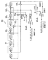
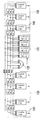
図21は、ECC回路を搭載した従来のNAND型フラッシュメモリの構成を簡略的に示すブロック図である。
このメモリは、8つのメモリセルエリア10,11,…,17から構成されている。各メモリセルエリア10〜17は、マトリクス状に配列された図示しない複数のメモリセルからなり、共通のワード線に接続された528個のメモリセルに対して528本のビット線を介して528ビットのデータ(=1ページ)を一括して書き込み及び読み出しができるようになっている。各メモリセルエリア10〜17には、528ビットの書き込みデータ及び読み出しデータを保持するページバッファ20〜27が接続されている。ページバッファ20〜27と、各メモリセルエリア10〜17毎に設けられたI/O端子40〜47との間には、各メモリセルエリア10〜17毎にECC回路30〜37がそれぞれ設けられている。
【0004】
各ECC回路30〜37は、各メモリセルエリア10〜17に記憶される1ページ分(528ビット)の情報ビットに対し、所定ビット数の検査ビット(ECC)を付加する符号化機能と、検査ビットが付加された情報ビットから所定ビット数の誤り検出及び誤り訂正を行う復号機能とを備えたもので、誤り訂正符号として、例えば比較的少ない回路規模で複数ビットの誤り訂正が可能なBCH(Bose-Chaudhuri-Hocquenghem)符号が使用されている。外部とメモリとの間は、例えばメモリセル数に対応する8ビット単位でデータがリード・ライトされる。従って、各ECC回路30〜37には、1ビットずつデータが入力され、内部の巡回型シフトレジスタを1ビットずつ巡回し、1ビットずつ出力することで、符号化処理及び復号処理が実行される。
【0005】
次に、BCH符号を利用した従来のECC回路30〜37の符号化及び復号動作ついて説明する。
なお、情報ビット数528ビットで、2ビット誤り訂正3ビット誤り検出を行うBCH符号の検査ビット数は21ビットになるが、ここでは説明を簡単にするため、情報ビット数k=7、符号長n=15、訂正ビット数t=2の2ビット誤り訂正3ビット誤り検出が可能なBCH符号を用いた誤り検出・訂正方式を例にとり説明する。
この場合の符号化、復号化に必要な生成多項式は以下のようになることが一般に知られている。
【0006】
【数1】

(1)符号化回路
図22は、従来のECC回路3i(i=0,1,…,又は7)の内部に機能的に構成される符号化回路10を示すブロック図である。この符号化回路10は、レジスタD7,D6,D5,D4,D3,D2,D1,D0からなるシフトレジスタ11と、モジュロ2の演算を行うXOR回路121,122,123,124と、切替スイッチSW1,SW2とから構成されている。
【0008】
シフトレジスタ11を1回動かす動作は、シフトレジスタ11の値をそれぞれX倍することに相当する。いま、シフトレジスタ11に格納されたデータの値を、次のように表す。
【0009】
【数2】
a0X0+a1X1+a2X2+a3X3+a4X4+a5X5+a6X6+a7X7
[但しaiはレジスタDiに格納された値でai=0又は1(i=0〜7)]
【0010】
これを1回シフトすることにより、
【0011】
【数3】
a0X1+a1X2+a2X3+a3X4+a4X5+a5X6+a6X7+a7X8
【0012】
となる。数1の生成多項式G(x)よりX8=X7+X6+X4+1の関係があるため、数3は、
【0013】
【数4】
a7X0+a0X1+a1X2+a2X3+(a3+a7)X4+a4X5+(a5+a7)X6+(a6+a7)X7
【0014】
のように表せる。これは各ビットをシフトさせた際に、レジスタD7の値a7をレジスタD0に格納し、レジスタD3,D7の値a3,a7をXOR回路121で足し込んでレジスタD4に格納し、レジスタD5,D7の値a5+a7をXOR回路122で足し込んでレジスタD6に格納し、レジスタD6,D7の値a6+a7をXOR回路123で足し込んでレジスタD7に格納することに相当する。
【0015】
符号化時には、まず、スイッチSW1,SW2がON側に接続され、I/O端子4iを介して外部から入力データ(情報ビット)I0,I1,I2,I3,I4,I5,I6(I0〜I6=0又は1)が1ビットずつ入力される。入力データI0〜I6が1ビット入力される毎に、シフトレジスタ11が1回動作する。データI0〜I6が入力されている間はスイッチSW1はONであるため、これらのデータがそのまま1ビットずつページバッファ2iに出力される。同時に、データI0〜I6は、XOR回路121でレジスタD7の値a7と足し込まれ、順次シフトレジスタ11に格納されていく。データI0〜I6のページバッファ2iへの入力が終了すると、シフトレジスタ11のレジスタD7,D6,D5,D4,D3,D2,D1,D0の内部には検査ビットI7,I8,I9,I10,I11,I12,I13,I14がそれぞれ格納された状態となる。その後、スイッチSW1,SW2は共にOFF側に接続され、シフトレジスタ11が動作する毎に、スイッチSW1を介して、検査ビットI7〜I14がページバッファ2iにシリアルに出力される。そして、ページバッファ2iに格納された情報ビットと検査ビットとがメモリセルエリア1iに記憶される。同時に、シフトレジスタ11の値はリセットされる。
【0016】
(2)復号回路
次に、復号回路について説明する。復号回路は、シンドローム計算回路と、誤り位置検出回路とから構成される。2ビット誤り訂正の場合、復号に際して2つのシンドロームS1,S3が必要であり、これらは最小多項式M1(x)=X4+X+1により求められることが知られている。図23(a)は、従来のS1シンドローム計算回路20を具体的に表した図、同図(b)は、従来のS3シンドローム計算回路30を示す図である。
【0017】
同図(a)のS1シンドローム計算回路20は、最小多項式M1(x)に基づき、レジスタD3,D2,D1,D0からなるシフトレジスタ21とXOR回路221,222とにより構成されている。ここでシフトレジスタ21を1回動かす動作はシフトレジスタ21の値をX倍することに相当する。いま、シフトレジスタ21に格納された値を、次のように表す。
【0018】
【数5】
a0X0+a1X1+a2X2+a3X3
[但しaiはレジスタDiに格納された値でai=0又は1(i=0〜3)]
【0019】
これを1回シフトすることにより
【0020】
【数6】
a0X1+a1X2+a2X3+a3X4
【0021】
となるが、αの最小多項式M1(x)よりX4=X+1の関係があるため、
【0022】
【数7】
a3X0+(a0+a3)X1+a1X2+a2X3
【0023】
となる。これは、各ビットをシフトさせた際に、レジスタD3の値a3をレジスタD0に格納し、レジスタD0,D3の値a0,a3をXOR回路122で足し込んでレジスタD1に格納することに相当する。メモリセルに記憶された情報ビットI0〜I6と検査ビットI7〜I14とは、この順にS1シンドローム計算回路20に1ビットずつ入力され、1ビット入力される毎に、シフトレジスタ21が1回動作する。全てのビットI0〜I14が入力されたらシフトレジスタ21(D0〜D3)にシンドロームS1が生成される。
【0024】
図23(b)のS3シンドローム計算回路30も、S1シンドローム計算回路20と同様にD3,D2,D1,D0からなるシフトレジスタ31及びXOR回路321,322,323,324からなり、最小多項式M1(x)のX3回路により構成されている。S3シンドローム計算回路30では、シフトレジスタ31を1回動かす動作はシフトレジスタ31の値をX3倍することに相当する。いま、シフトレジスタ31に格納された値を数5のように表し、これをX3すると、
【0025】
【数8】
a0X3+a1X4+a2X5+a3X6
【0026】
となるが、αの最小多項式M1(x)よりX4=X+1の関係があるため、
【0027】
【数9】
a1X0+(a1+a2)X1+(a2+a3)X2+(a0+a3)X3
【0028】
となる。これは、各ビットをシフトさせた際に、レジスタD1の値a1をレジスタD0に格納し、レジスタD1,D2の値a1,a2をXOR回路322で足し込んでレジスタD1に格納し、レジスタD2,D3の値a2,a3をXOR回路323で足し込んでレジスタD2に格納し、レジスタD0,D3の値a0,a3をXOR回路324で足し込んでレジスタD3に格納することに相当する。このS3シンドローム計算回路30にも、メモリセルに記憶された情報ビットI0〜I6と検査ビットI7〜I14とが、この順に1ビットずつ入力され、1ビット入力される毎に、シフトレジスタ31が1回動作する。全てのビットI0〜I14が入力されたらシフトレジスタ31(D0〜D3)にシンドロームS3が生成される。
【0029】
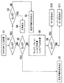
図24は、復号処理のアルゴリズムを示すフローチャートである。まず、S1,S2シンドローム計算回路20,30で、メモリセルエリア1iから読み出された情報ビットと検査ビットからシンドロームS1,S3を計算する(ステップS1)。シンドロームS1,S3が、S1=S3=0の場合、エラー無しとして読み出された情報ビットがそのまま出力される(ステップS2,S3,S4)。シンドロームS1,S3のうち、いずれか一方のみが0のときには、訂正不能としてデータがそのまま出力される(ステップS2,S3,S5,S6,S7)。S1≠0,S3≠0場合、計算を行ない、σ1=S1 2、σ2=S1 3+S3を求める(ステップS2,S6,S8)。ここでσ2=0の場合(ステップS9)、1ビットエラーがあることが分かるので、1ビット訂正して出力する(ステップS10)。σ2≠0の場合(ステップS9)、2ビットエラーがあることが分かるので、2ビット訂正して出力する(ステップS11)。
【0030】
誤りビットの位置は、数10に示す誤り位置多項式σ(Z)にZ=αI(I=0,1,2,3,4,5,6)を順次代入することによって求められることが一般に知られている。σ(αI)=0となったiが誤りの位置である。
【0031】
【数10】
σ(Z)=S1+σ1×Z+σ2×Z2
【0032】
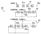
このような点に基づき構成された誤り位置検出回路の構成を図25及び図26に示す。図25は、S1、σ1及びσ2を計算すると共に格納する第1の演算部40aを示し、図26は、第1の演算部40aの演算結果に基づいて数10の演算を行ってデータの誤り位置を示す検出信号を出力する第2の演算部40bを示している。第1の演算部40aは、図25に示すようにシフトレジスタ41、X演算回路42及びX2演算回路43により構成されている。シフトレジスタ41aには、シンドロームS1が格納され、シフトレジスタ42a,43aにはσ1=S1 2、σ2=S1 3+S3の演算結果が格納される。ここでシフトレジスタ42aの値を、
【0033】
【数11】
a0X0+a1X1+a2X2+a3X3
[但しaiはレジスタDiに格納された値でai=0又は1(i=0〜3)]
【0034】
とすると、X演算回路42は、これをX倍するので、シフトレジスタ42aの値は、
【0035】
【数12】
a0X1+a1X2+a2X3+a3X4
【0036】
となるが、αの最小多項式M1(x)よりX4=X+1の関係があるため、数12は、
【0037】
【数13】
a3X0+(a0+a3)X1+a1X2+a2X3
【0038】
となる。これは、各ビットをシフトさせた際に、レジスタD3の値a3をレジスタD0に格納し、レジスタD0,D3の値a0,a3をXOR回路42bで足し込んでレジスタD1に格納することに相当する。
【0039】
また、X2演算回路43は、シフトレジスタ43aの値をX2倍するので、シフトレジスタ43aの値に数11で示す値が格納されているとすると、これをX2倍することにより、シフトレジスタ43aの値は、
【0040】
【数14】
a0X2+a1X3+a2X4+a3X5
【0041】
となるが、αの最小多項式M1(x)よりX4=X+1の関係があるため、数14は、
【0042】
【数15】
a2X0+(a2+a3)X1+(a0+a3)X2+a1X3
【0043】
となる。これは、各ビットをシフトさせた際に、レジスタE2の値a2をレジスタE0に格納し、レジスタE1の値a1をレジスタE3に格納し、レジスタE2,E3の値a2,a3をXOR回路43b1で足し込んでレジスタE1に格納し、レジスタE0,E3の値a0,a3をXOR回路43b2で足し込んでレジスタE2に格納することに相当する。
【0044】
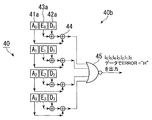
1ビットのデータI0〜I6の出力時、シフトレジスタ41a,42a,43aを1回動作させることにより、X演算回路42では、σ1の項がZ倍され、X2演算回路43では、σ2の項がZ2倍ずつされる。NAND型フラッシュメモリでは、メモリセルに記憶された情報ビットをチップの外部に出力する際のトグル信号に同期させてシフトレジスタ41a,42a,43aを動かす。これにより、第2の演算部40bでは、XOR回路44とNORゲート45とで演算された結果の出力が、誤り位置となったところで1となり、この出力で対応するデータIiを反転させることにより誤り検出訂正が行われる。
【0045】
【発明が解決しようとする課題】
このように、BCH符号を用いた従来のECC回路では、1ビットの入力に対し1回のシフト及び計算が基本動作となる。NAND型フラッシュメモリでは、1つのアドレスに対して8IO又は16IO等の単位で外部よりデータが並列に入力されるため、各IO毎に誤り訂正させるか、この一度の入力の間に8又は16回の計算を行なわなくてはならない。しかし、一度の入力の間に8又は16回の計算行なうことは、この部分のみ高速で動作させることを意味し、特別なプロセスなどが必要なため、現実には行なえない。
【0046】
そこで従来は、各メモリセルエリア1i(各I/O)毎にECC回路3iを設けて各メモリセルエリア1i単位で誤り訂正を行うようにしている。この場合、NAND型フラッシュメモリでは、1ページ(528バイト)単位でデータをリードしたり、プログラムしたりするので、各I/O毎に2ビット誤り訂正3ビット誤り検出をすると、情報ビット数は528ビット、検査ビット数は21ビットとなり、チップ全体で合計21×8=168ビットの余分な検査ビットが必要になる。これがチップの集積度を高める際の阻害要因となっていた。
【0047】
本発明は、このような問題点に鑑みなされたもので、情報ビット数に対する検査ビット数を削減してチップの集積度を向上させることができる半導体記憶装置を提供することを目的とする。
【0048】
【課題を解決するための手段】
本発明は、複数のメモリセルがマトリクス配列された複数のメモリセルエリアと、各メモリセルエリアのデータ入出力部に設けられて前記メモリセルエリアへの書き込みデータ及び前記メモリセルエリアからの読み出しデータを一時格納する複数のバッファと、前記各メモリセルエリアへの書き込み用のデータを外部から入力すると共に前記各メモリセルエリアから読み出されたデータを外部に出力する複数の入出力端子と、前記複数の入出力端子と前記複数のバッファとの間に設けられて前記複数のメモリセルエリアに書き込むデータに対して誤り訂正用の検査ビットを生成して付加する符号化器及び前記生成された検査ビットを使用して前記複数のメモリセルエリアから読み出されたデータに対して誤り訂正処理を行う復号器を備えた誤り訂正回路とを備えた半導体記憶装置において、前記誤り訂正回路は、1つの前記メモリセルエリアに対する書き込み及び読み出しの単位となるデータ(但し、検査ビットは含まれず)のビット数をMとしたとき、M×Nビット(Nは2以上の整数)を情報ビット長として1つの複数ビットからなる検査ビットを割り当て、符号化処理及び復号処理の少なくとも一方をNビットのデータを並列に処理して実行するものであり、前記符号化器は、情報ビット長k=M×N、符号長n、訂正ビット長tで定められる生成多項式G(X)から導かれる巡回符号を検査ビットとして生成するシフトレジスタ及び演算回路からなり、前記シフトレジスタは、次数を順番に異ならせたAビット(Aは2以上の整数)のデータを並列に入力し、1回のシフト動作で各データをXA倍し、M×N/A回のシフト動作で内部に前記検査ビットを生成するものであり、前記複数のバッファは、前記シフトレジスタのシフト動作に同期して前記データをAビットずつロードし、前記M×N/A回のシフト動作が終了したら前記生成された検査ビットをロードし、前記ロードされたデータと検査ビットとを前記複数のメモリセルエリアに書き込むことを特徴とする。
【0049】
本発明によれば、従来、各メモリセルエリアに対するアクセスの単位であるMビット毎に情報ビットを生成していたのに対し、Nビットの並列処理が可能になったことにより、M×Nビットに対して1つの検査ビットを割り当てることが可能になり、トータル的な情報ビットに対する検査ビット数を削減することができる。これにより、誤り訂正回路を搭載しつつチップの集積度を向上させることができる
一例を挙げると、tビット訂正(t+1)ビット誤り検出BCH符号では、
【0050】
【数16】
符号長 n=2m−1
情報ビット数 k≦2m−1−m×t
検査ビット数 mt+1≦n−k
訂正ビット数 t
【0051】
の関係があるため、mの数を大きくすると、符号長及び情報ビット数は指数関数的に増加するが、検査ビット数はそれほど増加しない。このため、情報ビット数は、2m−1−m×tを超えない限度で大きい方が情報ビット数に対する検査ビット数の割合が小さくなる。従って、できるだけ大きな情報ビット数に対し、検査ビットを設けた方が有利である。
例えば、NAND型フラッシュメモリは、1ページ(528バイト)でリードしたり、プログラムするが、各IO毎(メモリセルエリア毎)に2ビット誤り訂正3ビット誤り検出をすると、情報ビット数はk=528ビット、検査ビット数は21ビットとなるため、合計21×8=168ビットの余分な検査ビットが必要である。
しかし、1ページを1つの単位で、2ビット誤り訂正3ビット誤り検出をすると、情報ビット数が4224ビットのとき、検査ビット数は27ビットで良い。3ビット誤り訂正4ビット誤り検出としても、情報ビット数が4224ビットのとき、検査ビット数は40ビットで足りる。
【0052】
本発明の一つの実施形態においては、前記メモリセルエリアは、N個設けられている。符号化器は、例えば情報ビット長k=M×N、符号長n、訂正ビット長tで定められる生成多項式G(X)から導かれる巡回符号を検査ビットとして生成するシフトレジスタ及び演算回路からなり、前記シフトレジスタが、次数を順番に異ならせたNビットのデータを並列に入力し、1回のシフト動作で各データをXN倍し、M回のシフト動作で内部に前記検査ビットを生成するものである。
【0053】
また、復号器は、例えば前記情報ビットと検査ビットとを入力してシンドロームを計算するシンドローム計算回路と、前記計算されたシンドロームから誤り位置多項式の項を計算する第1の演算部及び計算された誤り多項式の項から誤り位置多項式を算出して誤り位置を検出する第2の演算部からなる誤り位置検出回路と、前記メモリセルエリアからバッファを介して読み出されたデータに対して前記検出された誤り位置でデータ反転処理を施すデータ反転回路とを備え、前記シンドローム計算回路が、情報ビット長k=M×N、符号長n、訂正ビット長tで定められるα演算子の最小多項式M(X)に基づく巡回符号をシンドロームとして生成するシフトレジスタ及び演算回路からなり、前記シフトレジスタが、次数を順番に異ならせたNビットのデータを並列に入力し、1回のシフト動作で各データをXKN(Kは整数)倍し、全ての前記情報ビット及び検査ビットが入力されることにより内部にシンドロームを生成するものである。
【0054】
また、誤り位置検出回路は、前記第2の演算部が、情報ビット長k=M×N、符号長n、訂正ビット長tで定められるα演算子の最小多項式M(X)に基づく巡回符号を誤り位置多項式の項として生成するシフトレジスタ及び演算回路からなり、前記シフトレジスタが、前記メモリエリアからのデータ出力に同期してシフト動作をし、各データをXK(Kは整数)倍し、順次、誤り訂正位置を検出するものである。
【0055】
前記符号化器、シンドローム計算回路及び第1の演算部は、演算用ロジック回路を構成するレジスタと演算回路とを切り替えて構成されるようにしても良い。また、復号器は、シンドローム又は誤り位置多項式の項を計算する際に使用されるガロア演算回路を更に含むようにしても良い。更に、前記第2の演算部は、例えば前記Nビットのデータに対してそれぞれ設けられたN個のローケータと、隣接するローケータ間に介挿されて隣接するローケータへのデータをXL倍するXL演算回路(Lは整数)とを備えたものである。
【0056】
【発明の実施の形態】
以下、図面を参照しながら、本発明の実施形態について説明する。
(1)第1の実施形態
まず、本発明を理解するため、第1の実施形態として、情報ビット数k=7、符号長n=15、訂正ビット数t=2の2ビット誤り訂正の例について説明する。
【0057】
(1−1)符号化回路
図22に示した従来の符号化回路10に入力データI0 が入力されると、この入力データI0は、XOR回路124によって符号化回路のX7の項に足しこまれ、その後X倍される。初期状態では符号化回路10の各レジスタ11の値は0であるため、この値を(0)とすると
【0058】
【数17】
(0+I0X7)X
【0059】
となる。次に入力データI1が符号化回路10に入力されると、この入力データI1は、符号化回路10のX7の項に足しこまれ、この後X倍されているので、
【0060】
【数18】
((0+I0X7)X+I1X7)X となる。
【0061】
次に入力データI2が符号化回路10に入力されると、この入力データI2は、符号化回路10のX7の項に足しこまれ、この後X倍されているので、
【0062】
【数19】
(((0+I0X7)X+I1X7)X+I2X7)X
【0063】
となる。
同様に、入力データI6まで符号化回路10に入力されると、
【0064】
【数20】
(((((((0+I0X7)X+I1X7)X+I2X7)X+I3 X7)X+I4X7)X+I5X7)X+I6X7)X
【0065】
となる。この式を変形すると
【0066】
【数21】
((((0+I0X7+I1X6)X2+I2X7+I3X6)X2+I4X7+I5X6)X2+I6X7)X
【0067】
となり、これは、入力データI0,I1がそれぞれ符号化回路10のX7,X6の項に足しこまれ、この後X2倍され、次に入力データI2,I3がそれぞれが符号化回路10のX7,X6の項に足しこまれ、この後X2倍され、次に入力データI4,I5がそれぞれが符号化回路10のX7,X6の項に足しこまれ、この後X2倍されることを意味する。つまり2ビットの入力の後、1回のシフトレジスタ11の動作でデータがX2倍される。但し、最後のI6は従来通り1ビットの入力で、X倍されることになる。
【0068】
ここで、シフトレジスタ11の値を、数2で示した値として、これをX2倍すると、
【0069】
【数22】
a0X2+a1X3+a2X4+a3X5+a4X6+a5X7+a6X8+a7X9
【0070】
となるが、数1の生成多項式G(x)よりX8=X7+X6+X4+1の関係があるため、数21は、
【0071】
【数23】
(a6+a7)X0+a7X1+a0X2+a1X3+(a2+a6+a7)X4+(a3+a7)X5+(a4+a6+a7)X6+(a5+a6)X7
【0072】
となる。
【0073】
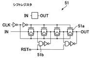
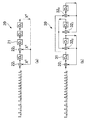
図1は数23を具体的に回路で構成した本実施形態に係る符号化回路50の構成を示すブロック図である。
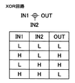
この符号化回路50は、レジスタD7,D6,D5,D4,D3,D2,D1,D0からなるシフトレジスタ51と、XOR回路521,522,523,524,525,526,527と、入力データ及び出力データを切り換えるための4つのスイッチSW11,SW12,SW21,SW22とから構成されている。シフトレジスタ51は、図2に示すように、リセット信号RSTnによりデータの内容がリセットされ、クロック信号CLKに同期して入力端子INから出力端子OUTへと1ビットのデータを転送する4段のトランスファーゲート51aと、必要なゲート回路51bとから構成されている。XOR回路52は、図3に示すように、入力端子IN1,IN2に入力されたデータにモジュロ2の演算を施して出力端子OUTから出力する。
【0074】
この符号化回路50は、数23に基づき、1回のシフト動作で、レジスタD6,D7の値a6,a7をXORゲート526で足し込んでレジスタD0に格納し、レジスタD7の値a7をレジスタD1に格納し、レジスタD0の値a0をレジスタD2に格納し、レジスタD1の値a1をレジスタD3に格納し、レジスタD2,D6,D7の値a2,a6,a7をXOR回路521,526で足し込んでレジスタD4に格納し、レジスタD3,D7の値a3,a7をXOR回路522で足し込んでレジスタD5に格納し、レジスタD4,D6,D7の値a4,a6,a7をXOR回路523,526で足し込んでレジスタD6に格納し、レジスタD5,D6の値a5,a6をXOR回路525で足し込んでレジスタD7に格納する。
【0075】
メモリに書き込まれるため外部から入力された入力データ(情報ビット)I0,I1,I2,I3,I4,I5,I6は、入力データI0,I2,I4と、入力データI1,I3,I5の2つに分割され、入力データI0,I2,I4がスイッチSW11,SW21のON側の端子に入力され、入力データI1,I3,I5がスイッチSW12,SW22のON側の端子に入力されている。つまり入力データは、2ビットづつ(I0,I1),(I2,I3),(I4,I5)の順で並列に入力され、入力後にシフトレジスタ51が1回動作する。但し、シフトレジスタ51は、1つおきに結線されているので、1回のシフト動作でデータがX2倍される。データ(I0,I1),(I2,I3),(I4,I5)が入力されている間は、スイッチSW11,SW21,SW12,SW22は全てONであり、これらのデータがそのまま2ビットずつ並列に出力される。同時に、データI0,I2,I4は、XOR回路527でレジスタD7の値a7と足し込まれ、順次シフトレジスタ51に格納され、データI1,I3,I5は、XOR回路524でレジスタD7の値a7と足し込まれ、順次シフトレジスタ51に格納されていく。但し、入力データの最後のI6は1ビットの入力であるため、図22に示した従来の符号化回路10と同じ結線状態に切り替わるようにする。このような切替を行うのは、情報ビット数としてk=7を選択したためである。データI0,I1,I2,I3,I4,I5,I6の入力が終了すると、シフトレジスタ51のレジスタD7,D6,D5,D4,D3,D2,D1,D0の内部には検査ビットI7,I8,I9,I10,I11,I12,I13,I14がそれぞれ格納された状態となる。その後、スイッチSW11,SW21,SW12,SW22は全てOFF側に接続され、シフトレジスタ51を動作させる毎に、SW11の出力に検査ビットI7,I9,I11,I13が出力され、SW12の出力に検査ビットI8,I10,I12,I14が出力される。同時に、シフトレジスタ51の値はリセットされる。これにより、2ビット入力の並列処理による検査ビットの生成が可能になる。
【0076】
(1−2)復号回路
▲1▼S1シンドローム計算回路
図23(a)の従来のS1シンドローム計算回路20では、まず、S1シンドローム計算回路20内の値がX倍された後、XOR回路221によりX0の項に入力データI0が足しこまれる。初期状態ではS1シンドローム計算回路20のシフトレジスタ21の値は0であるため、この値を(0)とすると、
【0077】
【数24】
0×X+I0
【0078】
となる。次にS1シンドローム計算回路20内の値がX倍された後、X0の項に入力データI1が足しこまれるので、
【0079】
【数25】
(0×X+I0)X+I1
【0080】
となる。続いてS1シンドローム計算回路20内の値がX倍された後、X0の項に入力データI2が足しこまれるので、
【0081】
【数26】
((0×X+I0)X+I1)X+I2
【0082】
となる。このようにして入力データI14までがS1シンドローム計算回路20に入力されると、
【0083】
【数27】
(((((((((((((0×X+I0)X+I1)X+I2)X+I3)X+I4)X+I5)X+ I6)X+I7)X+I8)X+I9)X+I10)X+I11)X+I12)X+I13)X+I14
【0084】
となる。この式を変形すると、
【0085】
【数28】
(((((((0×X2+I0X+I1)X2+I2X+I3)X2+I4X+I5)X2+I6X+I7)X2+I8X+I9)X2+I10X+I11)X2+I12X+I13)X+I14
【0086】
になり、これは、S1シンドローム計算回路20内の値をX2倍した後、入力データI0,がX1の項、入力データI1がX0の項にそれぞれ足しこまれ、次に、S1シンドローム計算回路20内の値をX2倍した後、入力データI2,がX1の項、入力データI3がX0の項にそれぞれ足しこまれ、次に、S1シンドローム計算回路20内の値をX2倍した後、入力データI4がX1の項、入力データI5がX0の項にそれぞれ足しこまれることを意味する。つまり1回のシフトレジスタの動作でデータがX2倍され、その後、2ビットのデータを入力している。但し、最後はS1シンドローム計算回路20内の値をX倍した後、1ビットの入力で入力データI14がX0の項に足しこまれている。
【0087】
ここで、シフトレジスタ21の値を、数5で示した値として、これをX2倍すると、
【0088】
【数29】
a0X2+a1X3+a2X4+a3X5
【0089】
となるが、αの最小多項式M1(x)より、X4=X+1の関係があるため、
【0090】
【数30】
a2X0+(a2+a3)X1+(a0+a3)X2+a1X3
【0091】
となる。
【0092】
図4(a)は数30を具体的に回路で構成した本実施形態に係るS1シンドローム計算回路60の構成を示すブロック図である。
このS1シンドローム計算回路60は、レジスタD0,D1,D2,D3からなるシフトレジスタ61と、XOR回路621,622,623,624とから構成されている。
【0093】
このS1シンドローム計算回路60は、数30に基づき、1回のシフト動作で、レジスタD2の値a2をレジスタD0に格納し、レジスタD2,D3の値a2,a3をXOR回路622で足し込んでレジスタD1に格納し、レジスタD0,D3の値a0,a3をXOR回路624で足し込んでレジスタD2に格納し、レジスタD1の値a1をレジスタD3に格納する。
【0094】
図示しないメモリセルエリアから読み出された情報ビットI0,I1,I2,I3,I4,I5,I6と、検査ビットI7,I8,I9,I10,I11,I12,I13,I14とは、I0,I2,I4,I6,I8,I10,I12,I14と、I1,I3,I5,I7,I9,I11,I13とに分割され、S1シンドローム計算回路60に2ビットづつ(I0,I1),(I2,I3),(I4,I5),…の順で並列に入力され、入力後にシフトレジスタ61が1回動作する。但し、シフトレジスタ61は、1つおきに結線されているので、1回のシフト動作でデータがX2倍される。データI0,I2,I4,…,I14は、XOR回路623でXOR回路622の出力a2+a3と足し込まれ、レジスタD1に格納され、データI1,I3,I5,…,I13は、XOR回路621でレジスタD2の値a2と足し込まれ、レジスタD0に格納される。但し、情報ビットの最後のI6は1ビットの入力であるため、図23の回路と同じ配線に切り替わる。又は、I15=0を、S1シンドローム計算回路60に入力させ、シフト動作させた後、シフトレジスタにX-1を掛ける。これにより、2ビット入力の並列処理が可能になる。
【0095】
▲2▼S3シンドローム計算回路
次に、図4(b)のS3シンドローム計算回路70について説明する。図23(b)の従来のS3シンドローム計算回路30では、まず、S3シンドローム計算回路30内の値がX3倍された後、XOR回路321によりX0の項に入力データI0が足しこまれる。初期状態では、S3シンドローム計算回路30のシフトレジスタ31の値は0であるため、この値を(0)とすると
【0096】
【数31】
0×X3+I0
【0097】
となる。次にS3シンドローム計算回路30内の値がX3倍された後、X0の項に入力データI1が足しこまれるので、
【0098】
【数32】
(0×X3+I0)X3+I1
【0099】
となる。続いてS3シンドローム計算回路30内の値がX3倍された後、X0の項に入力データI2が足しこまれるので、
【0100】
【数33】
((0×X3+I0)X3+I1)X3+I2
【0101】
となる。このようにして、入力データI14までがS3シンドローム計算回路30に入力されると、
【0102】
【数34】
(((((0X3+I0)X3+I1)X3+I2)X3+I3)X3+I4)X3+I5)X3+I6)X3+I7)X3+I8)X3+I9)X3+I10)X3+I11)X3+I12)X3+I13)X3+I14
【0103】
となる。この式を変形すると、
【0104】
【数35】
(((((0×X6+I0X3+I1)X6+I2X3+I3)X6+I4X3+I5)X6+I6X3+I7)X6+I8X3+I9)X6+I10X3+I11)X6+I12X3+I13) X3+I14
【0105】
になり、これは、S3シンドローム計算回路30内の値をX6倍した後、入力データI0がX3の項、入力データI1がX0の項にそれぞれ足しこまれ、次に、S3シンドローム計算回路30内の値をX6倍した後、入力データI2がX3の項、入力データI3がX0の項にそれぞれ足しこまれ、次にS3シンドローム計算回路30内の値をX6倍した後、入力データI4がX3の項、入力データI5がX0の項にそれぞれ足しこまれることを意味している。つまり1回のシフトレジスタの動作でデータがX6倍され、その後、2ビットのデータを入力している。但し、最後はS3シンドローム計算回路30内の値をX3倍した後、1ビットの入力で入力データI14がX0の項に足しこまれている。
【0106】
ここで、シフトレジスタ31の値を数5で示した値として、これをX6倍すると、
【0107】
【数36】
a0X6+a1X7+a2X8+a3X9
【0108】
となるが、αの最小多項式M1(x)よりX4=X+1の関係があるため、
【0109】
【数37】
(a1+a2)X0+(a1+a3)X1+(a0+a2)X2+(a0+a1+a3)X3
【0110】
となる。
【0111】
図4(b)は数37を具体的に回路で構成した本実施例に係るS3シンドローム計算回路70の構成を示すブロック図である。
このS3シンドローム計算回路70は、レジスタD0,D1,D2,D3からなるシフトレジスタ71と、XOR回路721,722,723,724,725,726とから構成されている。
【0112】
このS3シンドローム計算回路70は、数37に基づき、1回のシフト動作で、レジスタD1,D2の値a1,a2をXOR回路721で足し込んでレジスタD0に格納し、レジスタD1,D3の値a1,a3をXOR回路726で足し込んでレジスタD1に格納し、レジスタD0,D2の値a0,a2をXOR回路724で足し込んでレジスタD2に格納し、レジスタD0,D1,D3の値a0,a1,a3をXOR回路725,726で足し込んでレジスタD3に格納する。
【0113】
図示しないメモリセルエリアから読み出された情報ビットI0,I1,I2,I3,I4,I5,I6と、検査ビットI7,I8,I9,I10,I11,I12,I13,I14とは、I0,I2,I4,I6,I8,I10,I12,I14と、I1,I3,I5,I7,I9,I11,I13とに分割され、S3シンドローム計算回路70に2ビットづつ(I0,I1),(I2,I3),(I4,I5),…の順で並列に入力され、入力後シフトレジスタ71が1回動作する。データI0,I2,I4,…,I14は、XOR回路723でXOR回路726の出力a1+a3と足し込まれ、レジスタD1に格納され、データI1,I3,I5,…,I13は、XOR回路722でXOR回路721の出力a1+a2と足し込まれ、レジスタD0に格納される。但し、情報ビットの最後のI6は1ビットの入力であるため、図23のS3シンドローム計算回路30と同じ配線に切り替わる。又は、I15=0を、S3シンドローム計算回路70に入力させ、シフト動作させた後、シフトレジスタにX-3を掛ける。これにより、2ビット入力の並列処理が可能になる。
【0114】
▲3▼誤り位置検出回路
次に誤り位置検出回路について説明する。本実施形態の誤り位置検出回路では、S1,S3シンドローム計算回路60,70が1回のシフト動作で従来の2回分のシフト動作を行うものであるから、誤り位置検出回路も、従来の2回分のシフト動作に相当する演算を行う。いま、数10の誤り位置多項式を、
【0115】
【数38】
σ(Z)=S1+σ1×Z2+σ2×Z4
【0116】
とする。
図5及び図6は、数38に基づいて構成された誤り位置検出回路の構成を示す図である。
この誤り位置検出回路80は、S1、σ1及びσ2を計算すると共に格納する第1の演算部80a(図5)と、数38に基づいてデータの誤り位置を検出して検出信号を出力する第2の演算部80bとから構成されている。第1の演算部80aは、図5に示すようにシフトレジスタ81、X2演算回路82及びX4演算回路83により構成されている。シフトレジスタ81aには、初期状態としてシンドロームS1が格納され、シフトレジスタ82a,83aには初期状態としてσ1=S1 2、σ2=S1 3+S3の演算結果が格納される。この誤り位置検出回路80では、出力データI0,I1,I2,I3,I4,I5,I6のうち1つおきの出力データI0,I2,I4,I6、に同期して、誤り検出が行なわれ、シフトレジスタ81a,82a,83aを1回動作させることにより、X2演算回路82ではσ1の項がZ2倍、X4演算回路83では、σ2の項がZ4倍ずつされる。エラーがあるとσ=0となる。
【0117】
ここで、X2演算回路82は、図25のX2演算回路43と同一構成であり、シフトレジスタ43aとシフトレジスタ82aとが対応し、XOR回路43b1,43b2とXOR回路82b1,82b2とが対応するので、詳細な構成説明は割愛する。
【0118】
X4演算回路83は、数11に示すシフトレジスタ83aの値をX4倍するので、シフトレジスタ83aの値は、
【0119】
【数39】
a0X4+a1X5+a2X6+a3X7
【0120】
となるが、αの最小多項式M1(x)よりX4=X+1の関係があるため、
【0121】
【数40】
(a0+a3)X0+(a0+a1+a3)X1+(a1+a2)X2+(a2+a3)X3
【0122】
となる。これは、このX4演算回路83は、数40に基づき、1回のシフト動作で、レジスタE0,E3の値a0,a3をXOR回路83b1で足し込んでレジスタE0に格納し、レジスタE0,E1,E3の値a0,a1,a3をXOR回路83b1,83b2で足し込んでレジスタE1に格納し、レジスタE1,E2の値a1,a2をXOR回路83b3で足し込んでレジスタE2に格納し、レジスタE2,E3の値a2,a3をXOR回路83b4で足し込んでレジスタE3に格納する。
【0123】
図6の第2の演算部80bは、出力データI0,I2,I4,I6の誤り位置を検出する第1検出部84と、データI1,I3,I5の誤り位置を検出する第2検出部85と、データI1,I3,I5に関してσ1の項をZ倍するX演算回路86と、データI1,I3,I5に関してσ2の項をZ2倍するX2演算回路87とからなる。各検出部84,85のXOR回路88とNORゲート89とで演算された結果の出力が、誤り位置となったところで1となり、この出力で対応するデータIiを反転させることにより、1回のシフト動作で2ビット同時の並列的な誤り位置検出が可能になる。なお、X演算回路86、X2演算回路87の構成は図25及び図26に示した従来回路と同じであるが、データを記憶するためのレジスタは必要ない。
【0124】
(2)第2の実施形態
図7は、チップ上にECC回路を搭載した第2の実施形態に係るNAND型フラッシュメモリのブロック図である。
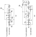
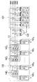
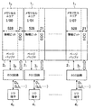
このメモリは、8つのメモリセルエリア1010,1011,…,1017を備えている。これらメモリセルエリア1010〜1017に対してメモリセルエリア1010〜1017への書き込みデータ(D0〜D7)及びメモリセルエリア1010〜1017からの読み出しデータ(D0〜D7)を一時格納する8つのページバッファ1020,1021,…,1027が設けられている。ページバッファ1020〜1027と、I/O端子1040,1041,…,1047との間には、書き込みデータに対する誤り訂正の検査ビットECCを生成すると共に、検査ビット(ECC)を使用して読み出しデータの誤り訂正を行うECC回路103が設けられている。このECC回路103は、従来のものとは異なり、全メモリセルエリア1010〜1017に対して1回にリード・ライトされる528ビット×8I/O=4224ビット分(M=528,N=8)のデータを情報ビットとし、これに共通の40ビットの検査ビットを付加して誤り検出訂正を行う。
【0125】
I/O端子105から入力されるアドレス及び制御信号は、それぞれ制御信号動作回路106及びアドレスデコーダ107に供給されている。制御信号動作回路106は、各種制御信号ALE,CLE,CE,WE,RE,WP等を入力して各部に供給する制御電圧を発生すると共に、外部回路にREADY/BUSY信号を出力する。アドレスデコーダ107は、外部からI/O端子105を介して入力されたアドレスを、一時的に記憶し、カラムデコーダ108及びブロック選択回路109を駆動する。カラムデコーダ108は、ページバッファ1020〜1021の各1つのカラムを活性化する。ブロック選択回路109は、メモリセルエリア1010〜1011中のワード線に読み出し、書き込み又は消去に必要な電圧を与える。
【0126】
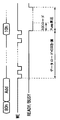
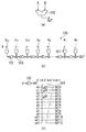
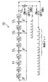
各メモリセルエリア101j(但し、j=0〜7)は、図8に示すように、電気的書換え可能な不揮発性メモリセルMCをマトリクス状に配列して構成されている。この例では、16個のメモリセルMCが1つの単位として直列に接続され、一方の端のメモリセルMCのドレインは、選択ゲートトランジスタSG1を介してビット線BLに接続され、他方の端のメモリセルMCのソースは、選択ゲートトランジスタSG2を介して共通ソース線SLに接続されている。ロウ方向のメモリセルMCの制御ゲートは、共通のワード線WLに接続され、ロウ方向の選択ゲートトランジスタSG1,SG2のゲート電極は、共通の選択ゲート線SGL1,SGL2に接続されている。この実施形態の場合、制御ゲート線に沿った1056個のメモリセルMCのうち、奇数番目と偶数番目にそれぞれ配置されたメモリセルMCに記憶される528ビットのデータが1回の書き込み及び読み出しの単位である1ページとなる。また、この例ではカラム方向に隣接する16ページ分のデータが1回の消去の単位である1ブロックとなる。但し、メモリセルエリア1017には、ワード線WLに沿った1056(528×2)個の情報ビット記憶用のメモリセルMCの他、誤り訂正用の検出ビットを80(40×2)ビット分記憶するためのメモリセルMCが設けられている。
【0127】
各ページバッファ102jは、図8に示すように、528個のデータ記憶回路121を備え、各データ記憶回路121は、それぞれ2本のビット線BLi,BLi+1に接続され、アドレスによって選択されたいずれか一方のビット線BLを介してメモリセルエリア101j中のメモリセルMCのデータを読み出したり、ビット線BLを介してメモリセルエリアMC中のメモリセルの状態を検出したり、ビット線BLを介してメモリセルエリア101j中のメモリセルMCに書き込み制御電圧を印加してメモリセルMCに書き込みを行う。528個のデータ記憶回路121のうち、いずれか1つのデータ記憶回路121がカラムデコーダ108によって選択され、選択されたデータ記憶回路121だけがECC回路103と接続される。
【0128】
従って、メモリ全体では、カラムデコーダ108により同一カラムアドレスを示す8ビット分(8IO分)のデータ記憶回路121とECC回路103とが接続される。読み出し動作のときは、図8の点線で示す1ページ分のメモリセルMCが選択され、528×8ビットのデータが一時に全てのデータ記憶回路121に記憶される。カラムデコーダ108は、外部より入力されるリードイネーブル(RE)信号に同期してカラムアドレスを1つずつインクリメントする。これにより、メモリセルエリア1010〜1017の各1つ、計8つのデータ記憶回路121が次々と選択され、順次8ビット分(8IO分)のデータがECC回路103に出力されることになる。書き込み動作のときも同様に、外部よりI/O端子1040〜1047を介して8ビット分(8IO分)のデータが順次ECC回路103に入力され、ECC回路103から順次8ビット分のデータが出力される。カラムデコーダ108は、外部より入力されるライトイネーブル(WE)信号に同期してカラムアドレスを、1づつインクリメントする。これにより、メモリセルエリア1010〜1017の各1つ、計8つのデータ記憶回路121が次々と選択され、ECC回路103からの8ビット分のデータが、選択された記憶回路121に入力されていく。
【0129】
次にECC回路103について詳細に説明する。
図9は、ECC回路103の詳細を示すブロック図である。ECC回路103は、複数段のレジスタ、XOR回路、スイッチ等から構成される演算用ロジック回路131と、シンドローム計算等に用いるガロア演算回路132と、復号時に動作する誤り位置検出回路133(主として第2の演算部)及びデータ反転回路134とを備えて構成されている。演算用ロジック回路131は、ECC回路103が符号化回路として機能するときには、検査ビット生成回路を構成し、ECC回路103が復号器として機能する場合には、シンドローム演算回路及び誤り位置検出回路の主として第1の演算部を構成する。
【0130】
(2−1)符号化回路
このECC回路103では、データを8ビット(D0〜D7)ずつ入力し、528×8=4224ビットのデータを単位として誤り検出訂正をおこなう。例えば、3ビット訂正4ビット誤り検出のBCH符号について考えると、情報ビットk=4224、符号長n=8191、訂正ビットt=3、m=13となり符号化及び復号に必要な生成多項式は以下のようになる。
【0131】
【数41】
先の第1の実施形態と同様に、数42を変形し、数43を求める。
【0133】
【数42】
(((((0+I0X39)X+I1X39)X+I2X39)X+I3X39)………
)X+I527X39)X
【0134】
【数43】
(((((0+I0X39+I1X38+I2X37……I7X32)X8+(I8X39……I15X32))X8………(I520X39+I521X38……I527X32)X8
【0135】
数43の意味するところは次の通りである。まず、一回のWE信号のクロックに対し入力される8ビットのデータD0〜D7=I0,I1,I2,…,I7のそれぞれにX39,X38,X37,…,X32を掛け、内部のレジスタ値に足しこみ、その後、レジスタの値をX8する。続いて、次のWE信号のクロックに対し入力される8ビットのデータD0〜D7=I8,I9,I10,…,I15のそれぞれにX39,X38,X37,…,X32を掛け、内部のレジスタ値に足しこみ、その後、レジスタの値をX8する。これを、最後の8ビットのデータD0〜D7=I4216,I4217,I4218,…,I4223まで528回繰り返す。
【0136】
図10は、演算用ロジック回路131に備えられた40段のレジスタREG0,REG1,…,REG39を示す。これらは符号化回路の巡回シフトレジスタを構成する。これらレジスタREG0〜REG39の入力をB0,B1,…,B39、出力をA0,A1,…,A39とする。演算用ロジック回路131は、上記数41の生成多項式と数43とに基づき、1回のデータ入力で下記数45及び数46に示すXOR演算を実行する。ここで使用されるXOR演算は数44に示される。レジスタREG32〜REG39は、出力A32〜A39を出力する前に、数45で示すように、外部より入力される8ビットのデータD0〜D7がレジスタ値にXOR演算により足しこまれた結果である出力AA32〜AA39を出力する。出力A0〜31、AA32〜AA39はXOR回路に繋がり、数46で示すXOR演算の結果B0〜39は、レジスタREG0〜REG39の入力に繋がり、シフトレジスタのクロックに同期し、取りこまれる。この演算を528回繰り返すと、演算ロジック回路131レジスタREG0〜REG39には、40ビットの検査ビットI4224,I4225,I4226,…,I4264が生成される。
【0137】
【数44】
【数45】
【数46】
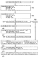
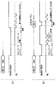
図11は、このECC回路103の符号化処理を示すフローチャート、図12は、同じく符号化処理のタイミングチャートである。
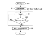
まず外部からデータ入力コマンド(80h)を入力すると(S21)、演算用ロジック回路131の内部のレジスタREG0〜40がリセットされ(S22)、次にアドレス(Add)が与えられる。続いてWE(ライトイネーブル)信号が外部から入力され、これに同期してデータが8ビットずつページバッファ102jにロードされる(S23,S24,S25)。これと同時にデータが演算用ロジック回路131に送りこまれ、検査ビットECCが計算される。カラムアドレスが最終の528に達したら(S25)、データロードを終了する。続いて外部よりプログラムコマンド(10h)が入力され、これによりメモリセルMCへのデータ書き込みのための図示しないチャージポンプによる昇圧動作が開始される。これと同時に、書込み動作を行なう前に、図示しない内部オシレータ等により40ビットのREG0〜REG39から順次5バイトずつ検査ビットが出力され、ページバッファ1027のデータ記憶回路121に格納される。この後、データ記憶回路121に格納されたデータが、外部アドレスAddにより選択された1ページ(図8の点線で示す)のメモリセルMCに記憶される。
【0141】
(2−2)復号回路
(1)シンドローム計算回路
3ビット誤り訂正、4ビット誤り検出のためには4つのシンドロームS0,S1,S3,S5が必要であることが知られている。シンドロームS0は最小多項式M0(x)=x+1により求められる。最小多項式M1(x)=x10+x3+1により求められるx10=x3+1をα演算子とすると、シンドロームS1はα演算子より、シンドロームS3はα3演算子より、シンドロームS5はα5演算子より求められる。従来の復号回路では、一回のWE信号のクロックに対し1ビットしか入力できなかったが、第1の実施形態の数27から数28に、また数34から数35に変形されたときと同様に変形し、一回のWE信号のクロックに対し8ビットのデータを取り込めるようにする。したがって、シンドロームS1はα8演算子より、シンドロームS3はα24演算子より、シンドロームS5はα40演算子より求められる。
【0142】
図13は、演算用ロジック回路131に備えられた40段のレジスタREG0〜REG39を示す。レジスタREG0はS0シンドローム計算回路の巡回シフトレジスタを構成し、レジスタREG1〜13はS1シンドローム計算回路の巡回シフトレジスタを構成し、レジスタREG14〜26はS3シンドローム計算回路の巡回シフトレジスタを構成し、レジスタREG27〜39はS5シンドローム計算回路の巡回シフトレジスタを構成する。ここで、レジスタREG0の入力をPP0、出力をP0、レジスタREG1〜13の入力をAA0,AA1,…,AA12、出力をA0,A1,…,A12、レジスタREG14〜26の入力をBB0,BB1,…,BB12、出力をB0,B1,…,B12、レジスタREG27〜39の入力をCC0,CC1,…,CC12、出力をC0,C1,…,C12とする。演算ロジック回路131は、1回のデータ入力で下記数47,数48,数49及び数50の演算を実行する。データ記憶回路121から読み出された、8ビットのデータD0〜D7と、それぞれのレジスタREG0〜REG39の出力P0、A0〜13、B0〜13、C0〜13とはXOR回路により足しこまれ、XOR回路の出力PP0、AA0〜13、BB0〜13、CC0〜13となり、レジスタREG0〜REG39の入力に繋がり、シフトレジスタのクロックに同期し、取りこまれる。レジスタREG1〜13に繋がるXOR回路はα8演算回路で、データD0〜D7の入力が加わっている。レジスタREG14〜REG26に繋がるXOR回路はα24演算回路で、データD0〜D7の入力が加わっている。レジスタREG27〜39に繋がるXOR回路はα40演算回路で、データD0〜D7の入力が加わっている。しかし、α40演算回路は回路規模が大きいため、図9に示したガロア演算回路132の片方の入力にα40を入力し、その出力とデータD0〜D7とをXOR回路で適宜演算して求めることも出来る。
【0143】
【数47】
【数48】
【数49】
【数50】
(2)誤り位置検出回路(第1の演算部)
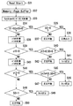
図14は、このECC回路103の復号処理を示すフローチャートである。
外部よりデータリードコマンド(00h)を入力した後、読み出すアドレス(Add)を入力することにより、リード動作が開始される(S31)。まず、アドレスにより選択された、1ページ(528バイト)分のメモリセルMCのデータをページバッファ1020〜1027に読み出す(S32)。この後、内部オシレータにより発振される信号に同期し、データD0〜D7が1バイトずつECC回路103に入力され、シンドロームを計算する(S33)。数47〜数50に示すように、シンドロームS0,S1,S3,S5を計算した後、S1=S3=S5=0 の場合(S34)で、S0=0だと(S35)エラー無し(正常出力:S36)となる。S0≠0(S35)では、訂正不能となる(S37)。S1=S3=S5=0でない場合(S34)、σ2=S1 2S3+S5 とσ0=S1 3+S3を計算する(S38)。σ0=0の場合(S39)で、σ2=0かつS0=0の場合(S40)、1ビットエラーがあるので1ビット訂正のアルゴリズムに移行する(S41)。σ2=0かつS0=0でない場合(S40)、訂正不能となる(S42)。σ0≠0の場合(S39)、σ1=S1(S1 3+S3) とσ3=(S1 3+S3)2+S1(S1 2 S3+S5)を計算する(S43)。σ3=0の場合(S44)で、σ2≠0かつS0=0の場合(S45)、2ビットエラーがあるので2ビット訂正するアルゴリズムに移行する(S46)。σ2≠0かつS0=0でない場合、訂正不能となる(S47)。σ3≠0の場合(S44)で、S0=1だと(S48)3ビットエラーがあるので3ビット訂正するアルゴリズムに移行する(S49)。但し、2ビット訂正と3ビット訂正のアルゴリズムは同じである。S0≠1だと(S48)訂正不能となる(S50)。
【0148】
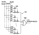
図15に、これらの計算を行う誤り位置検出回路を示す。この誤り位置検出回路は、演算用ロジック回路131に内蔵された各13ビットの4つのレジスタR,A,B,C及び図示しないXOR回路により構成される第1の演算部と、ガロア演算回路132と、8つのローケータ141及びこれらローケータ141の間に挿入された×α,×α2,×α3の演算を行う演算回路142からなる第2の演算部133と、これらの間を接続する13ビットのバスBUSR,BUSA,BUSB,BUSCとを備えて構成されている。ガロア演算回路132の出力はレジスタRに接続されている。
【0149】
図16は、誤り位置多項式の項であるσ0,σ1,σ3,σ2を算出するアルゴリズムを示している。レジスタA,B,CにシンドロームS1,S3,S5がそれぞれ格納されており、これらが全て0であればエラー無しなので、この演算は実行しない(S61)。そうでない場合、σ2=S1 2S3+S5の演算を行い、レジスタRに順次演算結果が格納されていき、最後に得られた演算結果がレジスタRからレジスタCに転送される(S62)。次に、σ0=S1 3+S3の演算を行い、レジスタRに順次演算結果が格納されていき、最後に得られた演算結果がレジスタRからレジスタBに転送される(S63)。レジスタB,Cに求められた演算結果が共に0であれば、1ビットエラーとして(S64)、1をレジスタRに格納し(S65)、そうでない場合には、σ1=S1(S1 3+S3)とσ3=(S1 3+S3)2+S1(S1 2 S3+S5)の演算を行う(S66,S67,S68)。
【0150】
一方、本実施形態では、符号長n=8191のうち情報ビットk=4224(528×8ビット)を誤り訂正するようにしているが、符号長n=8191の符号では、本来、情報ビットとして検査ビット40ビットを除いた8151ビットを持つことができる。このため、誤り位置は、8151−4224+1=3928ビット分だけずれていることになり、カラムアドレス0番地から読み出す場合、σ1にα3928、σ2にα7856(=3928×2)、σ3にα3593(=3928×3-8191)を掛ける計算を行なう(S69,S70,S71)。同様に、カラムアドレスi番地から読み出す場合、σ1にα3928+i、σ2にα7858(=(3928+i)×2)、σ3にα3596(=(3928+i)×3-8191)を掛ける計算を行なう。α3928+i等の係数は例えばROMに書きこんでおく。これらの係数はカラムアドレスiによるため、図7のカラムデコーダ108により選択されるカラムデータ記憶付近に、もしくはメモリセルエリア101内に格納する。又は、カラムアドレス0番地の係数のみ記憶し、他のアドレスがアクセスした場合は、誤り位置検出の動作をダミーで動かし係数を合わせるようにしても良い。
【0151】
図17は、ガロア演算回路132の詳細を示すブロック図である。
いま、同図(a)に示す13ビットの入力A,Bをそれぞれ、次のように示す。
【0152】
【数51】
A=a0X0+a1X1+a2X2+ … +a12X12
B=b0X0+b1X1+b2X2+ … +b12X12
【0153】
この場合、A×Bは、数52のようになる。
【0154】
【数52】
これを回路を表すと、図17(b)の構成となる。AとbiとがAND回路151でAND演算され、その演算結果をX乗算回路152でX倍して、XOR回路153で次のAとbi+1とのAND演算結果とXOR演算する。ここで、X乗算回路152は、同図(c)に示すように、数41のαの最小多項式M1(X)より、X13=X4+X3+X+1の関係があるので、X12の項がX0の項にシフトすると共に、XOR回路154により、X3,X1,X0の項に足し込まれ、それぞれX4,X3,X1の項に格納されるという演算を行う。
以上の演算の結果、13ビットのレジスタA,B,C,Rにはそれぞれ、σ1、σ3、σ2、σ0が初期値として与えられる。
【0156】
▲2▼誤り位置検出回路(第2の演算部)
誤りビットの位置の検出は、3ビット訂正と4ビット訂正の場合、下記数53の誤り位置多項式に従うことが知られている。
【0157】
【数53】
σ(Z)=S1+σ1×Z+σ2×Z2+σ3×Z3
【0158】
この数53にZ=αI(I=0,1,2,3・・・…)を順次代入してσ(αI)= 0となったiが誤りの位置となる。本実施形態では、一回のWEのクロックに対し8ビットのデータを出力するため、第1の実施形態で数10を数38に変形したように、数53を、次の数54のように変形する。
【0159】
【数54】
σ(Z)=σ0+σ1×Z8+σ2×Z16+σ3×Z24
【0160】
これにより、8ビットおきに8ビットずつ同時に誤り検出を行う。つまり8I/O分の出力データのうちI/O0に対して、誤り検出を行ない、誤りがあるとσ=0となる。図16の演算の結果、13ビットのシフトレジスタA,B,C,Rにはそれぞれ、σ1、σ3、σ2、σ0が初期値として与えられている、演算用ロジック回路131のシフトレジスタAに繋がるXOR回路はα8演算回路、シフトレジスタBに繋がるXORはα24演算回路、シフトレジスタCに繋がるXORはα16演算回路を構成する。レジスタAの入力をAA0,AA1,…,AA12、出力をA0,A1,…,A12、レジスタBの入力をBB0,BB1,…,BB12、出力をB0,B1,…,B12、レジスタCの入力をCC0,CC1,…,CC12、出力をC0,C1,…,C12とすると、これらのα8,α16,α24演算回路では、それぞれ数55,数56及び数57の演算を行う。
【0161】
【数55】
【数56】
【数57】
図18は、ローケータ141の具体的な構成を示す回路図である。ローケータ141は、XOR回路161とNOR回路162とからなり、σ(Z)を計算し、I/O0(j=0〜7)にエラーがある(σ= 0)とHを出力する。これにより、図9のデータ反転回路134で、このときのページバッファ1020のデータ記憶回路121のデータが反転されて出力される。一方、I/O1のデータに関しては、σ(Z)のσ1の項がZ倍、σ2の項がZ2倍、σ3の項がZ3倍された値なので、図15に示すように、σ1の項×Xを、σ2の項に×X2、σ3の項に×X3を演算する演算回路1421を搭載させ、その出力を、誤り位置多項式を解くためにローケータ1411に供給する。誤りが検出される(σ= 0)と、出力がHとなる。これらのX演算回路、X2演算回路、X3演算回路の入力をX0〜X12、出力Y0〜Y12とすると、これら演算回路は、次のような演算を実行する。これら演算回路には、データを記憶するためのレジスタは必要はない。
【0165】
【数58】
【数59】
【数60】
次に、I/O2のデータに関しては、σ(Z)のσ1の項がZ2倍、σ2の項がZ4倍、σ3の項がZ6倍された値であるが、I/O0を基準としてσ1の項×X2を、σ2の項に×X4、σ3の項に×X6を演算する演算回路を搭載させると、X6など大きな倍数の演算回路の回路規模が大きくなってしまう。このため、この実施形態では、演算回路1421の出力を再度、×X、×X2、×X3させる演算回路1411を設ける。以下、同様にしてI/O7のデータまで演算回路1427を配置する。
もし、I/O7までの信号伝搬遅延時間が問題となる場合には、図19に示すように、誤り位置検出回路(第2の演算部)133を構成する8つのローケータ141を演算用ロジック回路131の両側に4つずつ分割して配置することにより、ローケータ141までの信号伝搬路を1/2にすれば良い。
【0169】
図20は、このECC回路103の復号時のタイミングチャートである。同図(a)は、誤り位置多項式の項を全て計算してからデータの読み出しと誤り訂正とを行う場合を示している。
外部よりデータリードコマンド(00h)を入力した後、読み出すアドレス(Add)を入力することにより、READY/BUSY信号がアクティブになり、リード動作が開始される。まず、アドレスにより選択された、1ページ(528バイト)分のメモリセルMCのデータがページバッファ1020〜1027に読み出される。続いて、内部オシレータにより発振される信号に同期し、データD0〜D7が1バイトずつECC回路103に入力され、シンドロームが計算され、算出されたシンドロームS0,S1,S3,S5を用いて誤り位置多項式の項を演算する。その後、ライトイネーブル(RE)信号に同期してデータが読み出されると同時に、誤り訂正処理が実行される。この場合、ECC回路103がない場合に比べ、トータルのビジー時間の追加分は、シンドローム計算と誤り訂正用の演算子の計算時間分となり、1回のシンドローム計算に50ns、演算子の演算時間に3.6μsとすると、528×50ns+3.6μs=30μsとなる。
【0170】
同図(b)は、データの読み出しと同時にシンドロームS0,S1,S3,S5を計算するようにした例で、上記と同様にリード動作が開始され、1ページ(528バイト)分のメモリセルMCのデータがページバッファ1020〜1027に読み出されると、RE信号に同期してページバッファ1020〜1027からデータD0〜D7が1バイトずつ出力されると共にECC回路103でシンドローム計算が実行される。もし、シンドローム計算の結果、エラーが検出された場合には、ステータス・フェイルコマンド(70h)がアクティブになるので、誤り訂正用の演算子が計算され、その後、再度データを出力して誤り訂正を行う。この場合、エラーが無い場合、トータルのビジー時間の追加は0となる。
【0171】
ところで、情報ビットを528ビットとしたときと、情報ビットを4224ビットとしたときとでは、2ビット誤り訂正3ビット誤り検出をした場合、許容されるランダム不良数(デバイス不良確率が1ppmとなるときのランダム不良数)は、当然情報ビットを528ビットとしたときの方がよい。これを256Mビットの記憶容量のNAND型フラッシュメモリに適用した場合が表1となる。
表1より、情報ビット数が528ビットの2ビット訂正BCH符号では、許されるランダム不良数は100ビットであり、情報ビット数を4224ビットとすると30ビットしか許されなくなるが、3ビット訂正BCH符号で情報ビット数4224ビットでは、300ビットまでランダム不良を許し、また必要コードも40ビットと短い。更に、4ビット訂正BCH符号で情報ビット数4224ビットでは、1000ビットまでランダム不良が許容され、必要コードも53ビットと短いという効果がある。
【0172】
【表1】
ここで、128Mビットと512MビットのNAND型フラッシュメモリにECC回路を搭載しない場合、2ビット訂正の従来構成のECCを搭載した場合、2ビット訂正の本実施形態のECC回路を搭載した場合について、チップサイズで比較してみると、下記表2のようになる。
【0174】
【表2】
このように、本実施形態に係るECC回路を搭載したフラッシュメモリでは、従来型のECC回路搭載メモリがそれぞれ6.8%(128M),5.1%(512M)のチップサイズの増加があったのに対し、本実施形態のECC回路搭載メモリは、チップサイズの増加がその半分の3.2%(128M),2.5%(512M)であった。
【0176】
【発明の効果】
以上述べたように、本発明によれば、従来、各メモリセルエリアに対するアクセスの単位であるMビット毎に情報ビットを生成していたのに対し、Nビットの並列処理が可能になったことにより、M×Nビットに対して1つの検査ビットを割り当てることが可能になり、トータル的な情報ビットに対する検査ビット数を削減することができる。これにより、誤り訂正回路を搭載しつつチップの集積度を向上させることが可能になる。
【図面の簡単な説明】
【図1】 本発明の第1の実施形態に係るフラッシュメモリに搭載されるECC回路に使用される符号化器の構成を示すブロック図である。
【図2】 同符号化器に使用されるシフトレジスタの構成を示すブロック図である。
【図3】 同符号化器に使用されるXOR回路の真理値表である。
【図4】 同ECC回路に使用される復号器におけるシンドローム計算回路を示すブロック図である。
【図5】 同復号器に使用される誤り位置検出回路を構成する第1の演算部を示すブロック図である。
【図6】 同位置検出回路を構成する第2の演算部を示すブロック図である。
【図7】 本発明の第2の実施形態に係るNAND型フラッシュメモリのブロック図である。
【図8】 同フラッシュメモリのメモリセルエリアの構成を示す回路図である。
【図9】 同フラッシュメモリのECC回路を示すブロック図である。
【図10】 同ECC回路における符号化時の演算用ロジック回路を構成するレジスタを示す図である。
【図11】 同符号化回路の符号化処理を示すフローチャートである。
【図12】 同符号化処理のタイミングチャートである。
【図13】 同ECC回路における復号時の演算ロジック回路を構成するレジスタを示す図である。
【図14】 同復号処理を示すフローチャートである。
【図15】 同ECC回路における誤り位置検出回路のブロック図である。
【図16】 同誤り位置検出回路における誤り位置多項式の各項の算出アルゴリズムを示すフローチャートである。
【図17】 同ECC回路におけるガロア演算回路のブロック図である。
【図18】 同誤り位置検出回路の第2の演算部を示す図である。
【図19】 同ECC回路における誤り位置検出回路の他の例を示すブロック図である。
【図20】 同ECC回路における復号処理のタイミングチャートである。
【図21】 従来のECC回路を搭載したNAND型フラッシュメモリの構成を示すブロック図である。
【図22】 従来のECC回路における符号化器の構成を示すブロック図である。
【図23】 従来のECC回路の復号器におけるシンドローム計算回路を示すブロック図である。
【図24】 従来のECC回路の復号アルゴリズムを示すフローチャートである。
【図25】 従来のECC回路の誤り位置検出回路の第1の演算部を示すブロック図である。
【図26】 従来のECC回路の誤り位置検出回路の第2の演算部を示すブロック図である。
【符号の説明】
10〜17,1010〜1017…メモリセルエリア
20〜27,1020〜1027…ページバッファ
30〜37,103…ECC回路
40〜47,1040〜1047,105…I/O端子
10,50…符号化器
20,60…S1シンドローム計算回路
30,70…S3シンドローム計算回路
40,80,133…誤り位置検出回路
40a,80a…第1の演算部
40b,80b…第2の演算部
131…演算用ロジック回路、
132…ガロア演算回路
134…データ反転回路[0001]
BACKGROUND OF THE INVENTION
The present invention relates to a semiconductor memory device such as a NAND flash memory, and more particularly to a semiconductor memory device having an error correction function in a chip.
[0002]
[Prior art]
It is known that NAND-type flash memory has cell characteristics that deteriorate when rewriting is repeated and that data becomes garbled when left for a long time. Therefore, in order to increase the reliability of this type of NAND flash memory, a semiconductor memory in which an ECC (Error Correcting Code) circuit for error detection and correction is mounted in the chip has been proposed (for example, specially).Open 2000-348497, specialOpen 2001-14888 etc.).
[0003]
FIG. 21 is a block diagram schematically showing a configuration of a conventional NAND flash memory equipped with an ECC circuit.
This memory has 8
[0004]
Each
[0005]
Next, a
Note that the number of check bits of a BCH code that performs 528 bits of information and performs 2-bit error correction and 3-bit error detection is 21 bits, but here, for simplicity of explanation, the number of information bits k = 7, the code length An error detection / correction method using a BCH code capable of 2-bit error correction and 3-bit error detection with n = 15 and the number of correction bits t = 2 will be described as an example.
It is generally known that a generator polynomial necessary for encoding and decoding in this case is as follows.
[0006]
[Expression 1]
(1) Encoding circuit
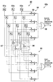
FIG. 22 is a block diagram showing an
[0008]
The operation of moving the
[0009]
[Expression 2]
a0X0+ A1X1+ A2X2+ AThreeXThree+ AFourXFour+ AFiveXFive+ A6X6+ A7X7
[However, aiIs register DiThe value stored ini= 0 or 1 (i = 0 to 7)]
[0010]
By shifting this once,
[0011]
[Equation 3]
a0X1+ A1X2+ A2XThree+ AThreeXFour+ AFourXFive+ AFiveX6+ A6X7+ A7X8
[0012]
It becomes. From the generator polynomial G (x) in
[0013]
[Expression 4]
a7X0+ A0X1+ A1X2+ A2XThree+ (AThree+ A7) XFour+ AFourXFive+ (AFive+ A7) X6+ (A6+ A7) X7
[0014]
It can be expressed as This is because register D is shifted when each bit is shifted.7Value a7Register D0And register DThree, D7Value aThree, A7XOR circuit 121Add register DFourAnd register DFive, D7Value aFive+ A7XOR circuit 122Add register D6And register D6, D7Value a6+ A7XOR circuit 12ThreeAdd register D7It is equivalent to storing in.
[0015]
At the time of encoding, first, the switches SW1 and SW2 are connected to the ON side, and input data (information bits) I from the outside via the I / O terminal 4i.0, I1, I2, IThree, IFour, IFive, I6(I0~ I6= 0 or 1) is input bit by bit. Input data I0~ I6Each
[0016]
(2) Decoding circuit
Next, the decoding circuit will be described. The decoding circuit includes a syndrome calculation circuit and an error position detection circuit. In the case of 2-bit error correction, two syndromes S are used for decoding.1, SThreeAre required and these are the minimum polynomial M1(X) = XFourIt is known to be obtained by + X + 1. FIG. 23A shows a conventional S.1A diagram specifically showing the
[0017]
S in FIG.1The
[0018]
[Equation 5]
a0X0+ A1X1+ A2X2+ AThreeXThree
[However, aiIs register DiThe value stored ini= 0 or 1 (i = 0 to 3)]
[0019]
By shifting this once
[0020]
[Formula 6]
a0X1+ A1X2+ A2XThree+ AThreeXFour
[0021]
The minimum polynomial M of α1X from (x)Four= X + 1 because there is a relationship
[0022]
[Expression 7]
aThreeX0+ (A0+ AThree) X1+ A1X2+ A2XThree
[0023]
It becomes. This is because register D is shifted when each bit is shifted.ThreeValue aThreeRegister D0And register D0, DThreeValue a0, AThreeXOR circuit 122Add register D1It is equivalent to storing in. Information bit I stored in the memory cell0~ I6And inspection bit I7~ I14Means S in this order1One bit at a time is input to the
[0024]
S in FIG.ThreeThe
[0025]
[Equation 8]
a0XThree+ A1XFour+ A2XFive+ AThreeX6
[0026]
The minimum polynomial M of α1X from (x)Four= X + 1 because there is a relationship
[0027]
[Equation 9]
a1X0+ (A1+ A2) X1+ (A2+ AThree) X2+ (A0+ AThree) XThree
[0028]
It becomes. This is because register D is shifted when each bit is shifted.1Value a1Register D0And register D1, D2Value a1, A2
[0029]
FIG. 24 is a flowchart showing an algorithm of the decoding process. First, S1, S2In the
[0030]
The position of the error bit is expressed by Z = α in the error position polynomial σ (Z) shown in Equation 10.IIt is generally known that it is obtained by sequentially substituting (I = 0, 1, 2, 3, 4, 5, 6). σ (αI) = 0, i is the error position.
[0031]
[Expression 10]
σ (Z) = S1+ Σ1× Z + σ2× Z2
[0032]
The configuration of an error position detection circuit configured based on such points is shown in FIGS. FIG.1, Σ1And σ2FIG. 26 shows a
[0033]
[Expression 11]
a0X0+ A1X1+ A2X2+ AThreeXThree
[However, aiIs register DiThe value stored ini= 0 or 1 (i = 0 to 3)]
[0034]
Then, since the X
[0035]
[Expression 12]
a0X1+ A1X2+ A2XThree+ AThreeXFour
[0036]
The minimum polynomial M of α1X from (x)Four= X + 1 because there is a relationship,
[0037]
[Formula 13]
aThreeX0+ (A0+ AThree) X1+ A1X2+ A2XThree
[0038]
It becomes. This is because register D is shifted when each bit is shifted.ThreeValue aThreeRegister D0And register D0, DThreeValue a0, AThreeIs added by the
[0039]
X2The
[0040]
[Expression 14]
a0X2+ A1XThree+ A2XFour+ AThreeXFive
[0041]
The minimum polynomial M of α1X from (x)Four= X + 1 because there is a relationship,
[0042]
[Expression 15]
a2X0+ (A2+ AThree) X1+ (A0+ AThree) X2+ A1XThree
[0043]
It becomes. This is because register E is shifted when each bit is shifted.2Value a2Register E0And register E1Value a1Register EThreeAnd register E2, EThreeValue a2, AThreeXOR circuit 43b1Register E1And register E0, EThreeValue a0, AThreeXOR circuit 43b2Register E2It is equivalent to storing in.
[0044]
1-bit data I0~ I6When the
[0045]
[Problems to be solved by the invention]
As described above, in the conventional ECC circuit using the BCH code, one shift and calculation for a 1-bit input is a basic operation. In the NAND flash memory, data is input from the outside in units of 8 IO or 16 IO for one address, so that error correction is performed for each IO or 8 or 16 times during this one input. Must be calculated. However, performing 8 or 16 calculations during one input means that only this part is operated at high speed, and a special process is required, so that it cannot be performed in reality.
[0046]
Therefore, conventionally, an ECC circuit 3i is provided for each memory cell area 1i (each I / O) to perform error correction in units of each memory cell area 1i. In this case, in the NAND flash memory, data is read or programmed in units of one page (528 bytes), so if 2-bit error correction 3-bit error detection is performed for each I / O, the number of information bits is 528 bits and the number of inspection bits are 21 bits, and a total of 21 × 8 = 168 bits of extra inspection bits are required for the entire chip. This has been an impediment to increasing the integration density of the chip.
[0047]
The present invention has been made in view of such problems, and an object of the present invention is to provide a semiconductor memory device that can reduce the number of inspection bits with respect to the number of information bits and improve the integration degree of the chip.
[0048]
[Means for Solving the Problems]
The present invention provides a plurality of memory cell areas in which a plurality of memory cells are arranged in a matrix, and write data to the memory cell area and read data from the memory cell area provided in a data input / output section of each memory cell area. A plurality of input / output terminals for inputting data for writing to each memory cell area from the outside and outputting data read from each memory cell area to the outside, An encoder that is provided between a plurality of input / output terminals and the plurality of buffers, and generates and adds an error correction check bit to data to be written to the plurality of memory cell areas, and the generated check An error is provided with a decoder that performs error correction processing on data read from the plurality of memory cell areas using bits. In the semiconductor memory device including the correction circuit, when the number of bits of data (however, a check bit is not included) serving as a unit of writing and reading with respect to one memory cell area is M, M × N bits (N is an integer of 2 or more) is used as an information bit length, one check bit consisting of a plurality of bits is assigned, and at least one of encoding processing and decoding processing is executed by processing N-bit data in parallel. The encoder includes a shift register that generates, as check bits, a cyclic code derived from a generator polynomial G (X) defined by an information bit length k = M × N, a code length n, and a correction bit length t. Comprising an arithmetic circuit, the shift register inputs A-bit data (A is an integer of 2 or more) having different orders in parallel, and performs one shift operation. In each of the data XAThe check bit is generated internally by M × N / A shift operations.The plurality of buffers load the data in units of A bits in synchronization with the shift operation of the shift register, and load the generated check bits when the M × N / A shift operations are completed, Writing the loaded data and check bits into the plurality of memory cell areasIt is characterized by that.
[0049]
According to the present invention, information bits are conventionally generated for each M bits, which is a unit of access to each memory cell area. However, since N bits can be processed in parallel, M × N bits Thus, one check bit can be assigned to the total number of check bits, and the number of check bits for the total information bits can be reduced. As a result, the integration degree of the chip can be improved while mounting the error correction circuit.
As an example, in a t-bit correction (t + 1) bit error detection BCH code,
[0050]
[Expression 16]
Code length n = 2m-1
Number of information bits k ≦ 2m−1−m × t
Number of inspection bits mt + 1 ≦ n−k
Number of correction bits t
[0051]
Therefore, if the number of m is increased, the code length and the number of information bits increase exponentially, but the number of check bits does not increase so much. For this reason, the number of information bits is 2mThe ratio of the number of check bits to the number of information bits becomes smaller as it is larger as long as it does not exceed −1−m × t. Therefore, it is advantageous to provide check bits for as many information bits as possible.
For example, a NAND flash memory reads or programs in one page (528 bytes), but when 2-bit error correction and 3-bit error detection are performed for each IO (each memory cell area), the number of information bits is k = Since 528 bits and the number of check bits are 21 bits, a total of 21 × 8 = 168 extra check bits are required.
However, when 2-bit error correction and 3-bit error detection are performed in one unit for one page, when the number of information bits is 4224 bits, the number of check bits may be 27 bits. Even for 3-bit error correction and 4-bit error detection, when the number of information bits is 4224 bits, the number of check bits is 40 bits.
[0052]
In one embodiment of the present invention, N memory cell areas are provided. The encoder is composed of, for example, a shift register and an arithmetic circuit that generate a cyclic code derived from a generator polynomial G (X) defined by an information bit length k = M × N, a code length n, and a correction bit length t as check bits. , The shift register inputs N-bit data having different orders in order, and inputs each data in one shift operation.NThe check bit is generated internally by M times of shift operations.
[0053]
The decoder also includes, for example, a syndrome calculation circuit that calculates a syndrome by inputting the information bits and check bits, a first calculation unit that calculates a term of an error locator polynomial from the calculated syndrome, and a calculation An error position detection circuit comprising a second calculation unit for detecting an error position by calculating an error position polynomial from an error polynomial term, and the detection for the data read from the memory cell area via a buffer. A data inversion circuit that performs data inversion processing at the error position, and the syndrome calculation circuit has a minimum polynomial M of an α operator defined by an information bit length k = M × N, a code length n, and a correction bit length t. X) based on a shift register that generates a cyclic code as a syndrome and an arithmetic circuit, and the shift register has N bits with different orders. Input data in parallel, and each data is X in one shift operation.KN(K is an integer) is multiplied and all the information bits and check bits are input to generate a syndrome inside.
[0054]
The error position detection circuit includes a cyclic code based on a minimum polynomial M (X) of an α operator defined by an information bit length k = M × N, a code length n, and a correction bit length t. Is generated as a term of an error position polynomial, and the shift register performs a shift operation in synchronization with the data output from the memory area, and outputs each data to XKThe error correction position is sequentially detected by multiplying (K is an integer).
[0055]
The encoder, the syndrome calculation circuit, and the first arithmetic unit may be configured by switching between a register and an arithmetic circuit constituting the arithmetic logic circuit. The decoder may further include a Galois arithmetic circuit used when calculating a syndrome or error locator polynomial term. In addition, the second arithmetic unit, for example, inserts N pieces of locators provided for each of the N-bit data and the adjacent locators into X data.LX to doubleLAnd an arithmetic circuit (L is an integer).
[0056]
DETAILED DESCRIPTION OF THE INVENTION
Hereinafter, embodiments of the present invention will be described with reference to the drawings.
(1) First embodiment
First, in order to understand the present invention, an example of 2-bit error correction with the number of information bits k = 7, the code length n = 15, and the number of correction bits t = 2 will be described as the first embodiment.
[0057]
(1-1) Coding circuit
In the
[0058]
[Expression 17]
(0 + I0X7) X
[0059]
It becomes. Next, input data I1Is input to the
[0060]
[Expression 18]
((0 + I0X7) X + I1X7) X
[0061]
Next, input data I2Is input to the
[0062]
[Equation 19]
(((0 + I0X7) X + I1X7) X + I2X7) X
[0063]
It becomes.
Similarly, input data I6Are input to the
[0064]
[Expression 20]
(((((((0 + I0X7) X + I1X7) X + I2X7) X + IThree X7) X + IFourX7) X + IFiveX7) X + I6X7) X
[0065]
It becomes. If this equation is transformed
[0066]
[Expression 21]
((((0 + I0X7+ I1X6) X2+ I2X7+ IThreeX6) X2+ IFourX7+ IFiveX6) X2+ I6X7) X
[0067]
This is the input data I0, I1Are X of the
[0068]
Here, it is assumed that the value of the
[0069]
[Expression 22]
a0X2+ A1XThree+ A2XFour+ AThreeXFive+ AFourX6+ AFiveX7+ A6X8+ A7X9
[0070]
From the generator polynomial G (x) of
[0071]
[Expression 23]
(A6+ A7) X0+ A7X1+ A0X2+ A1XThree+ (A2+ A6+ A7) XFour+ (AThree+ A7) XFive+ (AFour+ A6+ A7) X6+ (AFive+ A6) X7
[0072]
It becomes.
[0073]
FIG. 1 is a block diagram showing a configuration of an
The
[0074]
The
[0075]
Input data (information bit) I input from the outside because it is written to the memory0, I1, I2, IThree, IFour, IFive, I6Is the input data I0, I2, IFourAnd input data I1, IThree, IFiveInput data I0, I2, IFourIs input to the ON terminal of the switches SW11 and SW21, and the input data I1, IThree, IFiveIs input to the ON-side terminals of the switches SW12 and SW22. In other words, the input data is 2 bits at a time (I0, I1), (I2, IThree), (IFour, IFive) In parallel, and the
[0076]
(1-2) Decoding circuit
▲ 1 ▼ S1Syndrome calculation circuit
Conventional S in FIG.1In the
[0077]
[Expression 24]
0xX + I0
[0078]
It becomes. Then S1After the value in the
[0079]
[Expression 25]
(0xX + I0) X + I1
[0080]
It becomes. Followed by S1After the value in the
[0081]
[Equation 26]
((0 × X + I0) X + I1) X + I2
[0082]
It becomes. In this way, the input data I14Until S1When input to the
[0083]
[Expression 27]
((((((((((((0 × X + I0) X + I1) X + I2) X + IThree) X + IFour) X + IFive) X + I6) X + I7) X + I8) X + I9) X + ITen) X + I11) X + I12) X + I13) X + I14
[0084]
It becomes. If this equation is transformed,
[0085]
[Expression 28]
(((((((0 × X2+ I0X + I1) X2+ I2X + IThree) X2+ IFourX + IFive) X2+ I6X + I7) X2+ I8X + I9) X2+ ITenX + I11) X2+ I12X + I13) X + I14
[0086]
And this is S1The value in the
[0087]
Here, it is assumed that the value of the
[0088]
[Expression 29]
a0X2+ A1XThree+ A2XFour+ AThreeXFive
[0089]
The minimum polynomial M of α1From (x), XFour= X + 1 because there is a relationship
[0090]
[30]
a2X0+ (A2+ AThree) X1+ (A0+ AThree) X2+ A1XThree
[0091]
It becomes.
[0092]
FIG. 4A shows the S according to this embodiment in which
This S1
[0093]
This S1The
[0094]
Information bit I read from a memory cell area (not shown)0, I1, I2, IThree, IFour, IFive, I6And check bit I7, I8, I9, ITen, I11, I12, I13, I14Is I0, I2, IFour, I6, I8, ITen, I12, I14And I1, IThree, IFive, I7, I9, I11, I13And
[0095]
▲ 2 ▼ SThreeSyndrome calculation circuit
Next, S in FIG.ThreeThe
[0096]
[31]
0xXThree+ I0
[0097]
It becomes. Then SThreeThe value in the
[0098]
[Expression 32]
(0xXThree+ I0) XThree+ I1
[0099]
It becomes. Followed by SThreeThe value in the
[0100]
[Expression 33]
((0xXThree+ I0) XThree+ I1) XThree+ I2
[0101]
It becomes. In this way, the input data I14Until SThreeWhen input to the
[0102]
[Expression 34]
(((((0XThree+ I0) XThree+ I1) XThree+ I2) XThree+ IThree) XThree+ IFour) XThree+ IFive) XThree+ I6) XThree+ I7) XThree+ I8) XThree+ I9) XThree+ ITen) XThree+ I11) XThree+ I12) XThree+ I13) XThree+ I14
[0103]
It becomes. If this equation is transformed,
[0104]
[Expression 35]
(((((0 × X6+ I0XThree+ I1) X6+ I2XThree+ IThree) X6+ IFourXThree+ IFive) X6+ I6XThree+ I7) X6+ I8XThree+ I9) X6+ ITenXThree+ I11) X6+ I12XThree+ I13XThree+ I14
[0105]
And this is SThreeThe value in the
[0106]
Here, it is assumed that the value of the
[0107]
[Expression 36]
a0X6+ A1X7+ A2X8+ AThreeX9
[0108]
The minimum polynomial M of α1X from (x)Four= X + 1 because there is a relationship
[0109]
[Expression 37]
(a1+ A2) X0+ (A1+ AThree) X1+ (A0+ A2) X2+ (A0+ A1+ AThree) XThree
[0110]
It becomes.
[0111]
FIG. 4B shows the S according to the present embodiment in which
This SThree
[0112]
This SThreeThe
[0113]
Information bit I read from a memory cell area (not shown)0, I1, I2, IThree, IFour, IFive, I6And check bit I7, I8, I9, ITen, I11, I12, I13, I14Is I0, I2, IFour, I6, I8, ITen, I12, I14And I1, IThree, IFive, I7, I9, I11, I13And SThreeTwo bits each in the syndrome calculation circuit 70 (I0, I1), (I2, IThree), (IFour, IFive),... Are input in parallel, and the
[0114]
(3) Error position detection circuit
Next, the error position detection circuit will be described. In the error position detection circuit of this embodiment, S1, SThreeSince the
[0115]
[Formula 38]
σ (Z) = S1+ Σ1× Z2+ Σ2× ZFour
[0116]
And
5 and 6 are diagrams showing the configuration of the error position detection circuit configured based on the equation (38).
This error
[0117]
Where X2The
[0118]
XFourThe
[0119]
[39]
a0XFour+ A1XFive+ A2X6+ AThreeX7
[0120]
The minimum polynomial M of α1X from (x)Four= X + 1 because there is a relationship
[0121]
[Formula 40]
(A0+ AThree) X0+ (A0+ A1+ AThree) X1+ (A1+ A2) X2+ (A2+ AThree) XThree
[0122]
It becomes. This is because the X4
[0123]
The
[0124]
(2) Second embodiment
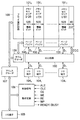
FIG. 7 is a block diagram of a NAND flash memory according to the second embodiment in which an ECC circuit is mounted on a chip.
This memory has eight
[0125]
The address and control signal input from the I /
[0126]
Each memory cell area 101j (where j = 0 to 7) is configured by arranging electrically rewritable nonvolatile memory cells MC in a matrix as shown in FIG. In this example, 16 memory cells MC are connected in series as one unit, the drain of the memory cell MC at one end is connected to the bit line BL via the selection gate transistor SG1, and the memory at the other end is connected. The source of the cell MC is connected to the common source line SL via the selection gate transistor SG2. The control gates of the memory cells MC in the row direction are connected to the common word line WL, and the gate electrodes of the selection gate transistors SG1 and SG2 in the row direction are connected to the common selection gate lines SGL1 and SGL2. In this embodiment, 528 bits of data stored in the odd-numbered and even-numbered memory cells MC out of 1056 memory cells MC along the control gate line are written and read once. One page is a unit. In this example, data for 16 pages adjacent in the column direction is one block which is a unit of one erase. However, the
[0127]
As shown in FIG. 8, each
[0128]
Therefore, in the entire memory, the
[0129]
Next, the
FIG. 9 is a block diagram showing details of the
[0130]
(2-1) Coding circuit
In the
[0131]
[Expression 41]
As in the first embodiment,
[0133]
[Expression 42]
(((((0 + I0X39) X + I1X39) X + I2X39) X + IThreeX39) ………
) X + I527X39) X
[0134]
[Expression 43]
(((((0 + I0X39+ I1X38+ I2X37...... I7X32) X8+ (I8X39...... I15X32)) X8……… (I520X39+ I521X38...... I527X32) X8
[0135]
The meaning of
[0136]
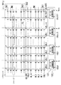
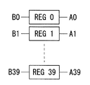
FIG. 10 shows 40 stages of registers REG0, REG1,..., REG39 provided in the
[0137]
(44)
[Equation 45]
[Equation 46]
FIG. 11 is a flowchart showing the encoding process of the
First, when a data input command (80h) is input from the outside (S21), the registers REG0 to REG40 in the
[0141]
(2-2)RecoveryCircuit
(1) Syndrome calculation circuit
Four syndromes S for 3-bit error correction and 4-bit error detection0, S1, SThree, SFiveIs known to be necessary. Syndrome S0Is the minimum polynomial M0It is obtained by (x) = x + 1. Minimum polynomial M1(X) = xTen+ XThreeX found by +1Ten= XThreeSyndrome S, where +1 is the α operator1Is the syndrome SThreeIs αThreeFrom the operator, syndrome SFiveIs αFiveIt is obtained from the operator. In the conventional decoding circuit, only one bit can be input with respect to the clock of one WE signal, but it is the same as when the first embodiment is changed from
[0142]
FIG. 13 shows 40-stage registers REG0 to REG39 provided in the
[0143]
[Equation 47]
[Formula 48]
[Equation 49]
[Equation 50]
(2) Error position detection circuit (first arithmetic unit)
FIG. 14 is a flowchart showing the decoding process of the
After inputting the data read command (00h) from the outside, the read operation is started by inputting the read address (Add) (S31). First, the data of the memory cell MC for one page (528 bytes) selected by the address is stored in the page buffer 102.0~ 1027(S32). Thereafter, in synchronization with the signal oscillated by the internal oscillator, the data D0 to D7 are input to the
[0148]
Figure 15 shows the error location for these calculations.detectionThe circuit is shown. The error position detection circuit includes a first arithmetic unit configured by four 13-bit registers R, A, B, and C incorporated in the
[0149]
FIG. 16 shows σ which is an error locator polynomial term.0, Σ1, ΣThree, Σ2The algorithm for calculating is shown. Syndrome S in registers A, B and C1, SThree, SFiveAre stored, and if they are all 0, there is no error, so this calculation is not executed (S61). Otherwise, σ2= S1 2SThree+ SFiveThe calculation results are sequentially stored in the register R, and the calculation result obtained last is transferred from the register R to the register C (S62). Next, σ0= S1 Three+ SThreeThe calculation results are sequentially stored in the register R, and the calculation result obtained last is transferred from the register R to the register B (S63). If the calculation results obtained in the registers B and C are both 0, a 1-bit error is stored (S64), 1 is stored in the register R (S65), and if not, σ1= S1(S1 Three+ SThree) And σThree= (S1 Three+ SThree)2+ S1(S1 2 SThree+ SFive) Is performed (S66, S67, S68).
[0150]
On the other hand, in this embodiment, the information bit k = 4224 (528 × 8 bits) is corrected in the code length n = 8191. However, the code having the code length n = 8191 is originally checked as an information bit. It can have 8151 bits excluding 40 bits. Therefore, the error position is shifted by 8151-4224 + 1 = 3928 bits, and when reading from
[0151]
FIG. 17 is a block diagram showing details of the Galois
Now, the 13-bit inputs A and B shown in FIG.
[0152]
[Formula 51]
A = a0X0+ A1X1+ A2X2+… + A12X12
B = b0X0+ B1X1+ B2X2+ ... + b12X12
[0153]
In this case, A × B is as shown in Formula 52.
[0154]
[Formula 52]
When this is expressed as a circuit, the configuration shown in FIG. A and bi are ANDed by AND
As a result of the above calculation, each of the 13-bit registers A, B, C, and R has σ1, ΣThree, Σ2, Σ0Is given as the initial value.
[0156]
(2) Error position detection circuit (second arithmetic unit)
It is known that the detection of the error bit position follows the error position polynomial of the following equation 53 in the case of 3-bit correction and 4-bit correction.
[0157]
[Equation 53]
σ (Z) = S1+ Σ1× Z + σ2× Z2+ ΣThree× ZThree
[0158]
In this number 53, Z = αI(I = 0, 1, 2, 3,...) Are sequentially substituted and σ (αI) = 0, i becomes the error position. In this embodiment, since 8-bit data is output for one WE clock, the equation 53 is changed into the following equation 54, as the
[0159]
[Formula 54]
σ (Z) = σ0+ Σ1× Z8+ Σ2× Z16+ ΣThree× Ztwenty four
[0160]
Thus, error detection is performed at the same time every 8 bits by 8 bits. That is, error detection is performed on I / O0 of the output data for 8 I / O, and σ = 0 if there is an error. As a result of the calculation in FIG. 16, the 13-bit shift registers A, B, C, and R1, ΣThree, Σ2, Σ0Is given as an initial value, the XOR circuit connected to the shift register A of the
[0161]
[Expression 55]
[56]
[Equation 57]
FIG. 18 is a circuit diagram showing a specific configuration of
[0165]
[Formula 58]
[Formula 59]
[Expression 60]
Next, for I / O2 data, σ of σ (Z)1Is the term Z2Times, σ2Is the term ZFourTimes, σThreeIs the term Z6The value multiplied by σ with reference to I / O01Term x2, Σ2XXFour, ΣThreeXX6When an arithmetic circuit that calculates6The circuit scale of a large multiple arithmetic circuit becomes large. Therefore, in this embodiment, the arithmetic circuit 1421Again, xX, xX2, XXThree
If the signal propagation delay time up to I / O 7 becomes a problem, as shown in FIG. 19, the eight
[0169]
FIG. 20 is a timing chart when the
After inputting the data read command (00h) from the outside and inputting the address (Add) to be read, the READY / BUSY signal becomes active and the read operation is started. First, the data of the memory cell MC for one page (528 bytes) selected by the address is stored in the page buffer 102.0~ 1027Is read out. Subsequently, in synchronization with the signal oscillated by the internal oscillator, the data D0 to D7 are input to the
[0170]
FIG. 5B shows the syndrome S at the same time as data reading.0, S1, SThree, SFiveIn this example, the read operation is started in the same manner as described above, and the data in the memory cell MC for one page (528 bytes) is stored in the page buffer 102.0~ 1027Read out to the page buffer 102 in synchronization with the RE signal.0~ 1027The data D0 to D7 are output byte by byte, and the syndrome calculation is executed by the
[0171]
By the way, when the information bit is set to 528 bits and the information bit is set to 4224 bits, when 2-bit error correction and 3-bit error detection are performed, the number of allowable random defects (when the device defect probability is 1 ppm) The number of random defects) is naturally better when the information bits are 528 bits. Table 1 shows the case where this is applied to a NAND flash memory having a storage capacity of 256 Mbits.
According to Table 1, in the 2-bit corrected BCH code having the number of information bits of 528 bits, the allowable number of random defects is 100 bits. If the number of information bits is 4224 bits, only 30 bits are allowed. In the information bit number 4224 bits, random defects are allowed up to 300 bits, and the necessary code is as short as 40 bits. Furthermore, with the 4-bit corrected BCH code and the number of information bits of 4224 bits, random defects are allowed up to 1000 bits, and the necessary code is also as short as 53 bits.
[0172]
[Table 1]
Here, when the ECC circuit is not mounted on the 128Mbit and 512Mbit NAND flash memory, when the ECC of the conventional configuration of 2-bit correction is mounted, and when the ECC circuit of the present embodiment of 2-bit correction is mounted, Table 2 below shows a comparison by chip size.
[0174]
[Table 2]
As described above, in the flash memory equipped with the ECC circuit according to this embodiment, the conventional ECC circuit mounted memory has an increase in chip size of 6.8% (128M) and 5.1% (512M), respectively. On the other hand, in the ECC circuit mounted memory of this embodiment, the increase in chip size was 3.2% (128M) and 2.5% (512M), half of that.
[0176]
【The invention's effect】
As described above, according to the present invention, information bits are generated for each M bits, which is a unit of access to each memory cell area, whereas N-bit parallel processing has become possible. Thus, one check bit can be assigned to M × N bits, and the number of check bits for total information bits can be reduced. As a result, it is possible to improve the integration density of the chip while mounting the error correction circuit.
[Brief description of the drawings]
FIG. 1 is a block diagram showing a configuration of an encoder used in an ECC circuit mounted on a flash memory according to a first embodiment of the present invention.
FIG. 2 is a block diagram showing a configuration of a shift register used in the encoder.
FIG. 3 is a truth table of an XOR circuit used in the encoder.
FIG. 4 is a block diagram showing a syndrome calculation circuit in a decoder used in the ECC circuit.
FIG. 5 is a block diagram showing a first calculation unit constituting an error position detection circuit used in the decoder.
FIG. 6 is a block diagram showing a second calculation unit constituting the position detection circuit.
FIG. 7 is a block diagram of a NAND flash memory according to a second embodiment of the present invention.
FIG. 8 is a circuit diagram showing a configuration of a memory cell area of the flash memory.
FIG. 9 is a block diagram showing an ECC circuit of the flash memory.
FIG. 10 is a diagram showing a register constituting an arithmetic logic circuit at the time of encoding in the ECC circuit.
FIG. 11 is a flowchart showing an encoding process of the encoding circuit.
FIG. 12 is a timing chart of the encoding process.
FIG. 13 is a diagram showing a register constituting an arithmetic logic circuit at the time of decoding in the ECC circuit.
FIG. 14 is a flowchart showing the decoding process.
FIG. 15 is a block diagram of an error position detection circuit in the ECC circuit.
FIG. 16 is a flowchart showing a calculation algorithm for each term of the error position polynomial in the error position detection circuit;
FIG. 17 is a block diagram of a Galois arithmetic circuit in the ECC circuit.
FIG. 18 is a diagram illustrating a second calculation unit of the error position detection circuit.
FIG. 19 is a block diagram showing another example of the error position detection circuit in the ECC circuit.
FIG. 20 is a timing chart of decoding processing in the ECC circuit.
FIG. 21 is a block diagram showing a configuration of a NAND flash memory equipped with a conventional ECC circuit.
FIG. 22 is a block diagram showing a configuration of an encoder in a conventional ECC circuit.
FIG. 23 is a block diagram showing a syndrome calculation circuit in a decoder of a conventional ECC circuit.
FIG. 24 is a flowchart showing a decoding algorithm of a conventional ECC circuit.
FIG. 25 is a block diagram showing a first calculation unit of an error position detection circuit of a conventional ECC circuit.
FIG. 26 is a block diagram showing a second calculation unit of an error position detection circuit of a conventional ECC circuit.
[Explanation of symbols]
10~ 17, 1010~ 1017... Memory cell area
20~ 27, 1020~ 1027... Page buffer
30~ 37, 103 ... ECC circuit
40~ 47, 1040~ 1047, 105 ... I / O terminals
10, 50 ... Encoder
20, 60 ... S1Syndrome calculation circuit
30, 70 ... SThreeSyndrome calculation circuit
40, 80, 133 ... error position detection circuit
40a, 80a ... 1st calculating part
40b, 80b ... second arithmetic unit
131 ... logic circuit for calculation,
132 ... Galois arithmetic circuit
134: Data inversion circuit
Claims (8)
各メモリセルエリアのデータ入出力部に設けられて前記メモリセルエリアへの書き込みデータ及び前記メモリセルエリアからの読み出しデータを一時格納する複数のバッファと、
前記各メモリセルエリアへの書き込み用のデータを外部から入力すると共に前記各メモリセルエリアから読み出されたデータを外部に出力する複数の入出力端子と、
前記複数の入出力端子と前記複数のバッファとの間に設けられて前記複数のメモリセルエリアに書き込むデータに対して誤り訂正用の検査ビットを生成して付加する符号化器及び前記生成された検査ビットを使用して前記複数のメモリセルエリアから読み出されたデータに対して誤り訂正処理を行う復号器を備えた誤り訂正回路と
を備えた半導体記憶装置において、
前記誤り訂正回路は、1つの前記メモリセルエリアに対する書き込み及び読み出しの単位となるデータ(但し、検査ビットは含まれず)のビット数をMとしたとき、M×Nビット(Nは2以上の整数)を情報ビット長として1つの複数ビットからなる検査ビットを割り当て、符号化処理及び復号処理の少なくとも一方をNビットのデータを並列に処理して実行するものであり、
前記符号化器は、情報ビット長k=M×N、符号長n、訂正ビット長tで定められる生成多項式G(X)から導かれる巡回符号を検査ビットとして生成するシフトレジスタ及び演算回路からなり、
前記シフトレジスタは、次数を順番に異ならせたAビット(Aは2以上の整数)のデータを並列に入力し、1回のシフト動作で各データをXA倍し、M×N/A回のシフト動作で内部に前記検査ビットを生成するものであり、
前記複数のバッファは、前記シフトレジスタのシフト動作に同期して前記データをAビットずつロードし、前記M×N/A回のシフト動作が終了したら前記生成された検査ビットをロードし、前記ロードされたデータと検査ビットとを前記複数のメモリセルエリアに書き込む
ことを特徴とする半導体記憶装置。A plurality of memory cell areas in which a plurality of memory cells are arranged in a matrix; and
A plurality of buffers provided in a data input / output section of each memory cell area to temporarily store write data to the memory cell area and read data from the memory cell area;
A plurality of input / output terminals for inputting data for writing to each memory cell area from the outside and outputting data read from each memory cell area to the outside;
An encoder that is provided between the plurality of input / output terminals and the plurality of buffers and generates and adds check bits for error correction to data to be written to the plurality of memory cell areas, and the generated In a semiconductor memory device comprising: an error correction circuit including a decoder that performs error correction processing on data read from the plurality of memory cell areas using a check bit;
The error correction circuit has M × N bits (N is an integer greater than or equal to 2), where M is the number of bits of data (however, the check bit is not included) as a unit of writing and reading with respect to one memory cell area ) Is assigned as one information bit length, and at least one of the encoding process and the decoding process is performed by processing N-bit data in parallel.
The encoder includes a shift register and an arithmetic circuit that generate a cyclic code derived from a generator polynomial G (X) defined by an information bit length k = M × N, a code length n, and a correction bit length t as check bits. ,
The shift register receives the data of the A bits having different orders in the order (A is an integer of 2 or more) in parallel, one shift operation each data multiplied by X A, M × N / A times der those in the shift operation to generate the check bits therein is,
The plurality of buffers load the data A bits at a time in synchronism with the shift operation of the shift register, load the generated check bits when the M × N / A shift operations are completed, and load the data A semiconductor memory device, wherein written data and check bits are written into the plurality of memory cell areas .
ことを特徴とする請求項2記載の半導体記憶装置。 Before SL shift register receives the N-bit data having different orders sequentially in parallel, each data in one shift operation multiplied by X N, generating the check bits therein by M times of shift operation The semiconductor memory device according to claim 2, wherein:
前記情報ビットと検査ビットとを入力してシンドロームを計算するシンドローム計算回路と、
前記計算されたシンドロームから誤り位置多項式の項を計算する第1の演算部及び計算された誤り多項式の項から誤り位置多項式を算出して誤り位置を検出する第2の演算部からなる誤り位置検出回路と、
前記メモリセルエリアからバッファを介して読み出されたデータに対して前記検出された誤り位置でデータ反転処理を施すデータ反転回路とを備え、
前記シンドローム計算回路は、情報ビット長k=M×N、符号長n、訂正ビット長tで定められるα演算子の最小多項式M(X)に基づく巡回符号をシンドロームとして生成するシフトレジスタ及び演算回路からなり、
前記シフトレジスタは、次数を順番に異ならせたNビットのデータを並列に入力し、1回のシフト動作で各データをXKN(Kは整数)倍し、全ての前記情報ビット及び検査ビットが入力されることにより内部にシンドロームを生成するものである
ことを特徴とする請求項2記載の半導体記憶装置。The decoder is
A syndrome calculation circuit for calculating a syndrome by inputting the information bit and the check bit;
Error position detection comprising a first calculation unit for calculating an error locator polynomial term from the calculated syndrome and a second calculation unit for calculating an error locator polynomial from the calculated error polynomial term and detecting an error position Circuit,
A data inversion circuit that performs data inversion processing at the detected error position on data read from the memory cell area via a buffer;
The syndrome calculation circuit includes a shift register and an operation circuit that generate a cyclic code based on a minimum polynomial M (X) of an α operator defined by an information bit length k = M × N, a code length n, and a correction bit length t as a syndrome. Consists of
The shift register inputs N-bit data having different orders in parallel, and multiplies each data by X KN (K is an integer) in one shift operation. The semiconductor memory device according to claim 2, wherein a syndrome is generated in response to the input.
前記情報ビットと検査ビットとを入力してシンドロームを計算するシンドローム計算回路と、
前記計算されたシンドロームから誤り位置多項式の項を計算する第1の演算部及び計算された誤り多項式の項から誤り位置多項式を算出して誤り位置を検出する第2の演算部からなる誤り位置検出回路と、
前記メモリセルエリアからバッファを介して読み出されたデータに対して前記検出された誤り位置でデータ反転処理を施すデータ反転回路とを備え、
前記第2の演算部は、情報ビット長k=M×N、符号長n、訂正ビット長tで定められるα演算子の最小多項式M(X)に基づく巡回符号を誤り位置多項式の項として生成するシフトレジスタ及び演算回路からなり、
前記シフトレジスタは、前記メモリエリアからのデータ出力に同期してシフト動作をし、各データをXK(Kは整数)倍し、順次、誤り訂正位置を検出するものである
ことを特徴とする請求項2記載の半導体記憶装置。The decoder is
A syndrome calculation circuit for calculating a syndrome by inputting the information bit and the check bit;
Error position detection comprising a first calculation unit for calculating an error locator polynomial term from the calculated syndrome and a second calculation unit for calculating an error locator polynomial from the calculated error polynomial term and detecting an error position Circuit,
A data inversion circuit that performs data inversion processing at the detected error position on data read from the memory cell area via a buffer;
The second arithmetic unit generates a cyclic code based on the minimum polynomial M (X) of the α operator defined by the information bit length k = M × N, the code length n, and the correction bit length t as an error position polynomial term. A shift register and an arithmetic circuit
The shift register performs a shift operation in synchronization with the data output from the memory area, multiplies each data by X K (K is an integer), and sequentially detects error correction positions. The semiconductor memory device according to claim 2.
前記Nビットのデータに対してそれぞれ設けられたN個のローケータと、
隣接するローケータ間に介挿されて隣接するローケータへのデータをXL倍するXL演算回路(Lは整数)と
を備えたものであることを特徴とする請求項4又は5記載の半導体記憶装置。The second calculation unit includes:
N locators provided for the N-bit data,
X L arithmetic circuit data to X L times to the adjacent locator adjacent interposed between locator (L is an integer) and a semiconductor memory according to claim 4 or 5, wherein the at those with apparatus.
Priority Applications (3)
| Application Number | Priority Date | Filing Date | Title |
|---|---|---|---|
| JP2001356571A JP4112849B2 (en) | 2001-11-21 | 2001-11-21 | Semiconductor memory device |
| US10/292,397 US7076722B2 (en) | 2001-11-21 | 2002-11-12 | Semiconductor memory device |
| US11/414,826 US7644342B2 (en) | 2001-11-21 | 2006-05-01 | Semiconductor memory device |
Applications Claiming Priority (1)
| Application Number | Priority Date | Filing Date | Title |
|---|---|---|---|
| JP2001356571A JP4112849B2 (en) | 2001-11-21 | 2001-11-21 | Semiconductor memory device |
Related Child Applications (1)
| Application Number | Title | Priority Date | Filing Date |
|---|---|---|---|
| JP2006126365A Division JP4113225B2 (en) | 2006-04-28 | 2006-04-28 | Semiconductor device |
Publications (2)
| Publication Number | Publication Date |
|---|---|
| JP2003157697A JP2003157697A (en) | 2003-05-30 |
| JP4112849B2 true JP4112849B2 (en) | 2008-07-02 |
Family
ID=19168071
Family Applications (1)
| Application Number | Title | Priority Date | Filing Date |
|---|---|---|---|
| JP2001356571A Expired - Lifetime JP4112849B2 (en) | 2001-11-21 | 2001-11-21 | Semiconductor memory device |
Country Status (2)
| Country | Link |
|---|---|
| US (2) | US7076722B2 (en) |
| JP (1) | JP4112849B2 (en) |
Families Citing this family (50)
| Publication number | Priority date | Publication date | Assignee | Title |
|---|---|---|---|---|
| JP4112849B2 (en) * | 2001-11-21 | 2008-07-02 | 株式会社東芝 | Semiconductor memory device |
| JP4550439B2 (en) * | 2003-02-28 | 2010-09-22 | 東芝メモリシステムズ株式会社 | ECC controller |
| JP4217887B2 (en) * | 2003-07-22 | 2009-02-04 | 日本電気株式会社 | Receiver |
| KR100546348B1 (en) * | 2003-07-23 | 2006-01-26 | 삼성전자주식회사 | Flash memory system and data writing method there-of |
| JP2005327437A (en) * | 2004-04-12 | 2005-11-24 | Nec Electronics Corp | Semiconductor storage device |
| US7099221B2 (en) * | 2004-05-06 | 2006-08-29 | Micron Technology, Inc. | Memory controller method and system compensating for memory cell data losses |
| KR101115843B1 (en) | 2004-05-06 | 2012-03-09 | 파나소닉 주식회사 | Semiconductor memory device |
| US20060010339A1 (en) * | 2004-06-24 | 2006-01-12 | Klein Dean A | Memory system and method having selective ECC during low power refresh |
| US7340668B2 (en) * | 2004-06-25 | 2008-03-04 | Micron Technology, Inc. | Low power cost-effective ECC memory system and method |
| US7116602B2 (en) * | 2004-07-15 | 2006-10-03 | Micron Technology, Inc. | Method and system for controlling refresh to avoid memory cell data losses |
| US6965537B1 (en) * | 2004-08-31 | 2005-11-15 | Micron Technology, Inc. | Memory system and method using ECC to achieve low power refresh |
| US7437653B2 (en) | 2004-12-22 | 2008-10-14 | Sandisk Corporation | Erased sector detection mechanisms |
| JP4791831B2 (en) * | 2006-01-20 | 2011-10-12 | 株式会社東芝 | Semiconductor memory device |
| JP4846384B2 (en) * | 2006-02-20 | 2011-12-28 | 株式会社東芝 | Semiconductor memory device |
| JP4836608B2 (en) * | 2006-02-27 | 2011-12-14 | 株式会社東芝 | Semiconductor memory device |
| DE102006010820A1 (en) | 2006-03-07 | 2007-09-13 | Micronas Gmbh | Error correction and error detection method for reading stored information data and memory controller therefor |
| JP2007305267A (en) * | 2006-05-15 | 2007-11-22 | Toshiba Corp | Semiconductor storage device |
| JP2008021390A (en) * | 2006-07-14 | 2008-01-31 | Toshiba Corp | Semiconductor storage device |
| KR100833600B1 (en) * | 2006-08-25 | 2008-05-30 | 삼성전자주식회사 | Error correction circuit, method there-of and semiconductor memory device including the circuit |
| JP4891704B2 (en) * | 2006-08-28 | 2012-03-07 | 株式会社東芝 | Semiconductor memory device |
| US7894289B2 (en) | 2006-10-11 | 2011-02-22 | Micron Technology, Inc. | Memory system and method using partial ECC to achieve low power refresh and fast access to data |
| US7900120B2 (en) | 2006-10-18 | 2011-03-01 | Micron Technology, Inc. | Memory system and method using ECC with flag bit to identify modified data |
| JP2008217857A (en) * | 2007-02-28 | 2008-09-18 | Toshiba Corp | Memory controller and semiconductor device |
| US8069395B2 (en) * | 2007-03-01 | 2011-11-29 | Cisco Technology, Inc. | Three bit error detection using ECC codes |
| US8042022B2 (en) | 2007-03-08 | 2011-10-18 | Micron Technology, Inc. | Method, system, and apparatus for distributed decoding during prolonged refresh |
| JP4621715B2 (en) * | 2007-08-13 | 2011-01-26 | 株式会社東芝 | Memory device |
| CN101140809A (en) * | 2007-09-07 | 2008-03-12 | 炬力集成电路设计有限公司 | Flash controller supporting pipelined error-correcting code and configurable operations and control method thereof |
| JP2009070509A (en) * | 2007-09-14 | 2009-04-02 | Oki Electric Ind Co Ltd | Semiconductor memory device |
| US7791974B2 (en) * | 2008-03-31 | 2010-09-07 | Intel Corporation | Recovery of existing SRAM capacity from fused-out blocks |
| US8023358B2 (en) * | 2008-04-02 | 2011-09-20 | International Business Machines Corporation | System and method for providing a non-power-of-two burst length in a memory system |
| JP2010009141A (en) * | 2008-06-24 | 2010-01-14 | Toshiba Corp | Data transfer method |
| JP2010097600A (en) * | 2008-09-22 | 2010-04-30 | Panasonic Corp | Semiconductor recording device |
| JP5259343B2 (en) * | 2008-10-31 | 2013-08-07 | 株式会社東芝 | Memory device |
| US20100198902A1 (en) * | 2009-02-03 | 2010-08-05 | Microsoft Corporation | Computing minimal polynomials of radical expressions |
| JP5350949B2 (en) * | 2009-09-11 | 2013-11-27 | Necエンベデッドプロダクツ株式会社 | Nonvolatile memory test method and memory test apparatus |
| US8533564B2 (en) * | 2009-12-23 | 2013-09-10 | Sandisk Technologies Inc. | System and method of error correction of control data at a memory device |
| JP5467270B2 (en) | 2010-04-28 | 2014-04-09 | 国立大学法人 東京大学 | Data input / output control device and semiconductor memory device system |
| TWI473105B (en) * | 2011-01-18 | 2015-02-11 | Macronix Int Co Ltd | Structure of ecc spare bits in three dimensional memory |
| US8615690B2 (en) * | 2011-05-05 | 2013-12-24 | Mediatek Inc. | Controller of memory device and method for operating the same |
| JP5346354B2 (en) * | 2011-05-17 | 2013-11-20 | シャープ株式会社 | Nonvolatile semiconductor memory device |
| US9471419B2 (en) * | 2013-03-12 | 2016-10-18 | Sandisk Technologies Llc | Systems and methods for performing data recovery in a memory system |
| JP5733766B2 (en) * | 2013-11-07 | 2015-06-10 | 国立大学法人 東京大学 | Data input / output control device and semiconductor memory device system |
| US9239756B2 (en) * | 2013-12-13 | 2016-01-19 | Sandisk Technologies Inc. | Systems and methods for performing data recovery in a memory system |
| US20150193301A1 (en) * | 2014-01-06 | 2015-07-09 | Kabushiki Kaisha Toshiba | Memory controller and memory system |
| US9720772B2 (en) | 2015-03-04 | 2017-08-01 | Kabushiki Kaisha Toshiba | Memory system, method for controlling magnetic memory, and device for controlling magnetic memory |
| US9659610B1 (en) * | 2016-05-18 | 2017-05-23 | Micron Technology, Inc. | Apparatuses and methods for shifting data |
| US10394648B2 (en) * | 2016-11-07 | 2019-08-27 | Samsung Electronics Co., Ltd. | Method to deliver in-DRAM ECC information through DDR bus |
| TWI643201B (en) * | 2017-11-27 | 2018-12-01 | 慧榮科技股份有限公司 | Encoder and associated encoding method and flash memory controller |
| CN109756235A (en) * | 2018-12-07 | 2019-05-14 | 天津津航计算技术研究所 | A kind of configurable parallel BCH error correction/encoding method |
| US20230267043A1 (en) * | 2022-02-23 | 2023-08-24 | Micron Technology, Inc. | Parity-based error management for a processing system |
Family Cites Families (44)
| Publication number | Priority date | Publication date | Assignee | Title |
|---|---|---|---|---|
| JPS62214599A (en) | 1986-03-14 | 1987-09-21 | Fujitsu Ltd | Semiconductor memory device |
| JPH03119835A (en) | 1989-10-03 | 1991-05-22 | Nippon Telegr & Teleph Corp <Ntt> | Error correction circuit |
| US5291496A (en) * | 1990-10-18 | 1994-03-01 | The United States Of America As Represented By The United States Department Of Energy | Fault-tolerant corrector/detector chip for high-speed data processing |
| US5226043A (en) * | 1990-12-27 | 1993-07-06 | Raytheon Company | Apparatus and method for data error detection and correction and address error detection in a memory system |
| JP2662472B2 (en) | 1991-06-13 | 1997-10-15 | シャープ株式会社 | Syndrome operation circuit for error correction processing |
| US5343426A (en) * | 1992-06-11 | 1994-08-30 | Digital Equipment Corporation | Data formater/converter for use with solid-state disk memory using storage devices with defects |
| JP3241851B2 (en) | 1993-03-18 | 2001-12-25 | 株式会社東芝 | Error correction decoding device |
| JPH09180496A (en) | 1995-12-28 | 1997-07-11 | Fujitsu Ltd | Semiconductor memory device |
| US5699368A (en) * | 1994-03-25 | 1997-12-16 | Mitsubishi Denki Kabushiki Kaisha | Error-correcting encoder, error-correcting decoder, and data transmitting system with error-correcting codes |
| JPH08167857A (en) | 1994-12-15 | 1996-06-25 | Mitsubishi Electric Corp | Decoding system |
| JP3272903B2 (en) * | 1995-03-16 | 2002-04-08 | 株式会社東芝 | Error correction detection circuit and semiconductor memory device |
| WO1996032674A2 (en) * | 1995-04-13 | 1996-10-17 | Cirrus Logic, Inc. | Semiconductor memory device for mass storage block access applications |
| US5757826A (en) * | 1995-07-12 | 1998-05-26 | Quantum Corporation | Word-wise processing for reed-solomon codes |
| US5754563A (en) * | 1995-09-11 | 1998-05-19 | Ecc Technologies, Inc. | Byte-parallel system for implementing reed-solomon error-correcting codes |
| JPH09162753A (en) | 1995-12-05 | 1997-06-20 | Fuji Electric Co Ltd | Decoding system for code word |
| JPH09288895A (en) * | 1996-04-19 | 1997-11-04 | Toshiba Corp | Ternary storage semiconductor storage system |
| US5740188A (en) * | 1996-05-29 | 1998-04-14 | Compaq Computer Corporation | Error checking and correcting for burst DRAM devices |
| US6308295B1 (en) * | 1996-10-08 | 2001-10-23 | Arizona Board Of Regents | Parallel spectral reed-solomon encoder and decoder |
| US5784391A (en) * | 1996-10-08 | 1998-07-21 | International Business Machines Corporation | Distributed memory system with ECC and method of operation |
| JPH10126280A (en) | 1996-10-18 | 1998-05-15 | Matsushita Electric Ind Co Ltd | Parallel process error correcting and decoding device |
| JPH10334697A (en) | 1997-05-28 | 1998-12-18 | Sony Corp | Semiconductor storage device nd error correction method therefor |
| US6360346B1 (en) * | 1997-08-27 | 2002-03-19 | Sony Corporation | Storage unit, method of checking storage unit, reading and writing method |
| JPH1173797A (en) | 1997-08-27 | 1999-03-16 | Sony Corp | Storage device |
| EP0969480A4 (en) * | 1998-01-21 | 2000-11-22 | Sony Corp | Encoding method and memory device |
| US6594794B1 (en) * | 1998-03-18 | 2003-07-15 | Stmicroelectronics S.R.L. | Reed-Solomon decoding of data read from DVD or CD supports |
| US6158040A (en) * | 1998-07-29 | 2000-12-05 | Neomagic Corp. | Rotated data-aligmnent in wade embedded DRAM for page-mode column ECC in a DVD controller |
| KR100287018B1 (en) * | 1998-08-07 | 2001-04-16 | 윤종용 | Semiconductor memory device with error correction circuit |
| JP4105819B2 (en) * | 1999-04-26 | 2008-06-25 | 株式会社ルネサステクノロジ | Storage device and memory card |
| JP2000348497A (en) | 1999-06-08 | 2000-12-15 | Toshiba Corp | Semiconductor memory device |
| JP4074029B2 (en) | 1999-06-28 | 2008-04-09 | 株式会社東芝 | Flash memory |
| KR100322542B1 (en) * | 1999-08-11 | 2002-03-18 | 윤종용 | Synchronous DRAM having ECC circuit implementing high speed pipeline operation and method of error check and correction of thereof |
| JP3975245B2 (en) * | 1999-12-16 | 2007-09-12 | 株式会社ルネサステクノロジ | Recording / reproducing apparatus and semiconductor memory |
| US6862662B1 (en) * | 2000-03-03 | 2005-03-01 | Micron Technology, Inc. | High density storage scheme for semiconductor memory |
| US6731538B2 (en) * | 2000-03-10 | 2004-05-04 | Kabushiki Kaisha Toshiba | Semiconductor memory device including page latch circuit |
| JP4707803B2 (en) * | 2000-07-10 | 2011-06-22 | エルピーダメモリ株式会社 | Error rate determination method and semiconductor integrated circuit device |
| US20030120858A1 (en) * | 2000-09-15 | 2003-06-26 | Matrix Semiconductor, Inc. | Memory devices and methods for use therewith |
| US6661730B1 (en) * | 2000-12-22 | 2003-12-09 | Matrix Semiconductor, Inc. | Partial selection of passive element memory cell sub-arrays for write operation |
| JP2002251884A (en) * | 2001-02-21 | 2002-09-06 | Toshiba Corp | Semiconductor memory and system device therefor |
| US6957378B2 (en) * | 2001-06-04 | 2005-10-18 | Kabushiki Kaisha Toshiba | Semiconductor memory device |
| US7051264B2 (en) * | 2001-11-14 | 2006-05-23 | Monolithic System Technology, Inc. | Error correcting memory and method of operating same |
| JP4112849B2 (en) * | 2001-11-21 | 2008-07-02 | 株式会社東芝 | Semiconductor memory device |
| JP3914839B2 (en) * | 2002-07-11 | 2007-05-16 | エルピーダメモリ株式会社 | Semiconductor memory device |
| JP4102313B2 (en) * | 2004-02-05 | 2008-06-18 | 株式会社東芝 | Semiconductor integrated circuit device |
| JP4191100B2 (en) * | 2004-06-18 | 2008-12-03 | エルピーダメモリ株式会社 | Semiconductor memory device |
-
2001
- 2001-11-21 JP JP2001356571A patent/JP4112849B2/en not_active Expired - Lifetime
-
2002
- 2002-11-12 US US10/292,397 patent/US7076722B2/en not_active Expired - Lifetime
-
2006
- 2006-05-01 US US11/414,826 patent/US7644342B2/en not_active Expired - Lifetime
Also Published As
| Publication number | Publication date |
|---|---|
| US20030101405A1 (en) | 2003-05-29 |
| US7076722B2 (en) | 2006-07-11 |
| US7644342B2 (en) | 2010-01-05 |
| JP2003157697A (en) | 2003-05-30 |
| US20060195766A1 (en) | 2006-08-31 |
Similar Documents
| Publication | Publication Date | Title |
|---|---|---|
| JP4112849B2 (en) | Semiconductor memory device | |
| JP4856110B2 (en) | Chain search apparatus and chain search method | |
| US7581153B2 (en) | Memory with embedded error correction codes | |
| US5621682A (en) | Memory system | |
| US8339854B2 (en) | Nonvolatile memory device and data randomizing method thereof | |
| JP5043562B2 (en) | Error correction circuit, method thereof, and semiconductor memory device including the circuit | |
| US8291303B2 (en) | Memory device with error correction system for detection and correction errors in read out data | |
| US20070157064A1 (en) | Systems and methods for error corrections | |
| US7366971B2 (en) | Semiconductor memory having sub-party cell array error correction | |
| JP3272903B2 (en) | Error correction detection circuit and semiconductor memory device | |
| US8990667B2 (en) | Error check and correction circuit, method, and memory device | |
| US20090319863A1 (en) | Error-correcting system of semiconductor memory, error-correcting method, and memory system with error-correcting system | |
| JP2010518464A (en) | Semiconductor memory device | |
| US20030061560A1 (en) | Method for error detection/correction of multilevel cell memory and multilevel cell memory having error detection/correction function | |
| TWI479317B (en) | Memory system | |
| JP4113225B2 (en) | Semiconductor device | |
| US7075851B2 (en) | Semiconductor memory device inputting/outputting data and parity data in burst operation | |
| JP2001202792A (en) | Error correction encoding method for semiconductor memory, and semiconductor storage device | |
| JP2014033364A (en) | Error detection and correction circuit and memory device | |
| CN108665940B (en) | ECC encoding circuit, decoding circuit and memory controller | |
| JP5617776B2 (en) | MEMORY CIRCUIT, MEMORY DEVICE, AND MEMORY DATA ERROR CORRECTION METHOD | |
| KR100377490B1 (en) | Nonvolatile semiconductor memory device | |
| JP2007328894A (en) | Semiconductor storage device, and method of inspecting thereof | |
| US11831335B2 (en) | Memory system and control method of controlling nonvolatile memory | |
| JPH10334697A (en) | Semiconductor storage device nd error correction method therefor |
Legal Events
| Date | Code | Title | Description |
|---|---|---|---|
| A621 | Written request for application examination |
Free format text: JAPANESE INTERMEDIATE CODE: A621 Effective date: 20040929 |
|
| A131 | Notification of reasons for refusal |
Free format text: JAPANESE INTERMEDIATE CODE: A131 Effective date: 20070828 |
|
| A521 | Written amendment |
Free format text: JAPANESE INTERMEDIATE CODE: A523 Effective date: 20071029 |
|
| A02 | Decision of refusal |
Free format text: JAPANESE INTERMEDIATE CODE: A02 Effective date: 20071225 |
|
| A521 | Written amendment |
Free format text: JAPANESE INTERMEDIATE CODE: A523 Effective date: 20080225 |
|
| A911 | Transfer to examiner for re-examination before appeal (zenchi) |
Free format text: JAPANESE INTERMEDIATE CODE: A911 Effective date: 20080317 |
|
| TRDD | Decision of grant or rejection written | ||
| A01 | Written decision to grant a patent or to grant a registration (utility model) |
Free format text: JAPANESE INTERMEDIATE CODE: A01 Effective date: 20080408 |
|
| A61 | First payment of annual fees (during grant procedure) |
Free format text: JAPANESE INTERMEDIATE CODE: A61 Effective date: 20080410 |
|
| R151 | Written notification of patent or utility model registration |
Ref document number: 4112849 Country of ref document: JP Free format text: JAPANESE INTERMEDIATE CODE: R151 |
|
| FPAY | Renewal fee payment (event date is renewal date of database) |
Free format text: PAYMENT UNTIL: 20110418 Year of fee payment: 3 |
|
| FPAY | Renewal fee payment (event date is renewal date of database) |
Free format text: PAYMENT UNTIL: 20130418 Year of fee payment: 5 |
|
| FPAY | Renewal fee payment (event date is renewal date of database) |
Free format text: PAYMENT UNTIL: 20140418 Year of fee payment: 6 |
|
| S111 | Request for change of ownership or part of ownership |
Free format text: JAPANESE INTERMEDIATE CODE: R313111 |
|
| R350 | Written notification of registration of transfer |
Free format text: JAPANESE INTERMEDIATE CODE: R350 |
|
| EXPY | Cancellation because of completion of term |