WO2025115409A1 - 半導体装置 - Google Patents
半導体装置 Download PDFInfo
- Publication number
- WO2025115409A1 WO2025115409A1 PCT/JP2024/035952 JP2024035952W WO2025115409A1 WO 2025115409 A1 WO2025115409 A1 WO 2025115409A1 JP 2024035952 W JP2024035952 W JP 2024035952W WO 2025115409 A1 WO2025115409 A1 WO 2025115409A1
- Authority
- WO
- WIPO (PCT)
- Prior art keywords
- region
- trench
- conductivity type
- conductivity
- regions
- Prior art date
- Legal status (The legal status is an assumption and is not a legal conclusion. Google has not performed a legal analysis and makes no representation as to the accuracy of the status listed.)
- Pending
Links
Images



Classifications
-
- H—ELECTRICITY
- H10—SEMICONDUCTOR DEVICES; ELECTRIC SOLID-STATE DEVICES NOT OTHERWISE PROVIDED FOR
- H10D—INORGANIC ELECTRIC SEMICONDUCTOR DEVICES
- H10D12/00—Bipolar devices controlled by the field effect, e.g. insulated-gate bipolar transistors [IGBT]
- H10D12/01—Manufacture or treatment
- H10D12/031—Manufacture or treatment of IGBTs
- H10D12/032—Manufacture or treatment of IGBTs of vertical IGBTs
- H10D12/038—Manufacture or treatment of IGBTs of vertical IGBTs having a recessed gate, e.g. trench-gate IGBTs
-
- H—ELECTRICITY
- H10—SEMICONDUCTOR DEVICES; ELECTRIC SOLID-STATE DEVICES NOT OTHERWISE PROVIDED FOR
- H10D—INORGANIC ELECTRIC SEMICONDUCTOR DEVICES
- H10D12/00—Bipolar devices controlled by the field effect, e.g. insulated-gate bipolar transistors [IGBT]
- H10D12/01—Manufacture or treatment
- H10D12/031—Manufacture or treatment of IGBTs
- H10D12/032—Manufacture or treatment of IGBTs of vertical IGBTs
- H10D12/035—Etching a recess in the emitter region
-
- H—ELECTRICITY
- H10—SEMICONDUCTOR DEVICES; ELECTRIC SOLID-STATE DEVICES NOT OTHERWISE PROVIDED FOR
- H10D—INORGANIC ELECTRIC SEMICONDUCTOR DEVICES
- H10D12/00—Bipolar devices controlled by the field effect, e.g. insulated-gate bipolar transistors [IGBT]
- H10D12/411—Insulated-gate bipolar transistors [IGBT]
- H10D12/417—Insulated-gate bipolar transistors [IGBT] having a drift region having a doping concentration that is higher at the collector side relative to other parts of the drift region
-
- H—ELECTRICITY
- H10—SEMICONDUCTOR DEVICES; ELECTRIC SOLID-STATE DEVICES NOT OTHERWISE PROVIDED FOR
- H10D—INORGANIC ELECTRIC SEMICONDUCTOR DEVICES
- H10D12/00—Bipolar devices controlled by the field effect, e.g. insulated-gate bipolar transistors [IGBT]
- H10D12/411—Insulated-gate bipolar transistors [IGBT]
- H10D12/418—Insulated-gate bipolar transistors [IGBT] having a drift region having a doping concentration that is higher at the emitter side relative to other parts of the drift region
-
- H—ELECTRICITY
- H10—SEMICONDUCTOR DEVICES; ELECTRIC SOLID-STATE DEVICES NOT OTHERWISE PROVIDED FOR
- H10D—INORGANIC ELECTRIC SEMICONDUCTOR DEVICES
- H10D12/00—Bipolar devices controlled by the field effect, e.g. insulated-gate bipolar transistors [IGBT]
- H10D12/411—Insulated-gate bipolar transistors [IGBT]
- H10D12/441—Vertical IGBTs
- H10D12/461—Vertical IGBTs having non-planar surfaces, e.g. having trenches, recesses or pillars in the surfaces of the emitter, base or collector regions
- H10D12/481—Vertical IGBTs having non-planar surfaces, e.g. having trenches, recesses or pillars in the surfaces of the emitter, base or collector regions having gate structures on slanted surfaces, on vertical surfaces, or in grooves, e.g. trench gate IGBTs
-
- H—ELECTRICITY
- H10—SEMICONDUCTOR DEVICES; ELECTRIC SOLID-STATE DEVICES NOT OTHERWISE PROVIDED FOR
- H10D—INORGANIC ELECTRIC SEMICONDUCTOR DEVICES
- H10D30/00—Field-effect transistors [FET]
- H10D30/01—Manufacture or treatment
-
- H—ELECTRICITY
- H10—SEMICONDUCTOR DEVICES; ELECTRIC SOLID-STATE DEVICES NOT OTHERWISE PROVIDED FOR
- H10D—INORGANIC ELECTRIC SEMICONDUCTOR DEVICES
- H10D30/00—Field-effect transistors [FET]
- H10D30/60—Insulated-gate field-effect transistors [IGFET]
- H10D30/64—Double-diffused metal-oxide semiconductor [DMOS] FETs
- H10D30/66—Vertical DMOS [VDMOS] FETs
-
- H—ELECTRICITY
- H10—SEMICONDUCTOR DEVICES; ELECTRIC SOLID-STATE DEVICES NOT OTHERWISE PROVIDED FOR
- H10D—INORGANIC ELECTRIC SEMICONDUCTOR DEVICES
- H10D62/00—Semiconductor bodies, or regions thereof, of devices having potential barriers
- H10D62/10—Shapes, relative sizes or dispositions of the regions of the semiconductor bodies; Shapes of the semiconductor bodies
- H10D62/102—Constructional design considerations for preventing surface leakage or controlling electric field concentration
- H10D62/103—Constructional design considerations for preventing surface leakage or controlling electric field concentration for increasing or controlling the breakdown voltage of reverse-biased devices
- H10D62/105—Constructional design considerations for preventing surface leakage or controlling electric field concentration for increasing or controlling the breakdown voltage of reverse-biased devices by having particular doping profiles, shapes or arrangements of PN junctions; by having supplementary regions, e.g. junction termination extension [JTE]
- H10D62/106—Constructional design considerations for preventing surface leakage or controlling electric field concentration for increasing or controlling the breakdown voltage of reverse-biased devices by having particular doping profiles, shapes or arrangements of PN junctions; by having supplementary regions, e.g. junction termination extension [JTE] having supplementary regions doped oppositely to or in rectifying contact with regions of the semiconductor bodies, e.g. guard rings with PN or Schottky junctions
- H10D62/107—Buried supplementary regions, e.g. buried guard rings
-
- H—ELECTRICITY
- H10—SEMICONDUCTOR DEVICES; ELECTRIC SOLID-STATE DEVICES NOT OTHERWISE PROVIDED FOR
- H10D—INORGANIC ELECTRIC SEMICONDUCTOR DEVICES
- H10D62/00—Semiconductor bodies, or regions thereof, of devices having potential barriers
- H10D62/10—Shapes, relative sizes or dispositions of the regions of the semiconductor bodies; Shapes of the semiconductor bodies
- H10D62/124—Shapes, relative sizes or dispositions of the regions of semiconductor bodies or of junctions between the regions
- H10D62/126—Top-view geometrical layouts of the regions or the junctions
- H10D62/127—Top-view geometrical layouts of the regions or the junctions of cellular field-effect devices, e.g. multicellular DMOS transistors or IGBTs
-
- H—ELECTRICITY
- H10—SEMICONDUCTOR DEVICES; ELECTRIC SOLID-STATE DEVICES NOT OTHERWISE PROVIDED FOR
- H10D—INORGANIC ELECTRIC SEMICONDUCTOR DEVICES
- H10D62/00—Semiconductor bodies, or regions thereof, of devices having potential barriers
- H10D62/10—Shapes, relative sizes or dispositions of the regions of the semiconductor bodies; Shapes of the semiconductor bodies
- H10D62/13—Semiconductor regions connected to electrodes carrying current to be rectified, amplified or switched, e.g. source or drain regions
- H10D62/141—Anode or cathode regions of thyristors; Collector or emitter regions of gated bipolar-mode devices, e.g. of IGBTs
- H10D62/142—Anode regions of thyristors or collector regions of gated bipolar-mode devices
-
- H—ELECTRICITY
- H10—SEMICONDUCTOR DEVICES; ELECTRIC SOLID-STATE DEVICES NOT OTHERWISE PROVIDED FOR
- H10D—INORGANIC ELECTRIC SEMICONDUCTOR DEVICES
- H10D62/00—Semiconductor bodies, or regions thereof, of devices having potential barriers
- H10D62/50—Physical imperfections
- H10D62/53—Physical imperfections the imperfections being within the semiconductor body
-
- H—ELECTRICITY
- H10—SEMICONDUCTOR DEVICES; ELECTRIC SOLID-STATE DEVICES NOT OTHERWISE PROVIDED FOR
- H10D—INORGANIC ELECTRIC SEMICONDUCTOR DEVICES
- H10D64/00—Electrodes of devices having potential barriers
- H10D64/111—Field plates
- H10D64/117—Recessed field plates, e.g. trench field plates or buried field plates
-
- H—ELECTRICITY
- H10—SEMICONDUCTOR DEVICES; ELECTRIC SOLID-STATE DEVICES NOT OTHERWISE PROVIDED FOR
- H10D—INORGANIC ELECTRIC SEMICONDUCTOR DEVICES
- H10D8/00—Diodes
- H10D8/422—PN diodes having the PN junctions in mesas
-
- H—ELECTRICITY
- H10—SEMICONDUCTOR DEVICES; ELECTRIC SOLID-STATE DEVICES NOT OTHERWISE PROVIDED FOR
- H10D—INORGANIC ELECTRIC SEMICONDUCTOR DEVICES
- H10D84/00—Integrated devices formed in or on semiconductor substrates that comprise only semiconducting layers, e.g. on Si wafers or on GaAs-on-Si wafers
- H10D84/101—Integrated devices comprising main components and built-in components, e.g. IGBT having built-in freewheel diode
- H10D84/161—IGBT having built-in components
-
- H—ELECTRICITY
- H10—SEMICONDUCTOR DEVICES; ELECTRIC SOLID-STATE DEVICES NOT OTHERWISE PROVIDED FOR
- H10D—INORGANIC ELECTRIC SEMICONDUCTOR DEVICES
- H10D84/00—Integrated devices formed in or on semiconductor substrates that comprise only semiconducting layers, e.g. on Si wafers or on GaAs-on-Si wafers
- H10D84/80—Integrated devices formed in or on semiconductor substrates that comprise only semiconducting layers, e.g. on Si wafers or on GaAs-on-Si wafers characterised by the integration of at least one component covered by groups H10D12/00 or H10D30/00, e.g. integration of IGFETs
Definitions
- the present invention relates to a semiconductor device.
- Patent Document 1 describes that "a plurality of doping regions (e.g., implantation regions) 1059 of a second conductivity type (complementary to the first conductivity type) are created below the bottoms of the exposed trenches 14, 15, and 16.”
- Patent Document 2 describes providing a "narrow FWD region 19a" and a "wide FWD region 19b.”
- Patent Documents [Patent Documents] [Patent Document 1] JP 2019-110288 A [Patent Document 2] Japanese Patent No. 5637175 A
- a semiconductor device in a first aspect of the present invention, includes a transistor portion and a diode portion, the semiconductor device including a first conductivity type drift region provided in a semiconductor substrate, a plurality of trench portions extending in a predetermined trench extension direction on the front surface side of the semiconductor substrate, and a second conductivity type collector region provided below the drift region.
- the transistor portion may include a second conductivity type base region provided above the drift region, a first conductivity type emitter region having a doping concentration higher than that of the drift region, a second conductivity type first contact region having a doping concentration higher than that of the base region, a plurality of second conductivity type trench bottom regions repeatedly provided in the trench extension direction below the base region, and a plurality of trench bottomless regions repeatedly provided in the trench extension direction and sandwiched between the plurality of trench bottom regions.
- the diode portion may include a second conductivity type anode region provided above the drift region and a back side region provided below the drift region.
- the back surface side region may include a first conductivity type portion of a first conductivity type and a second conductivity type portion of a second conductivity type.
- the first conductivity type portion and the second conductivity type portion may be provided to form a repeating structure in which a second conductivity type forming region in which the second conductivity type portion is formed and a second conductivity type non-forming region in which the second conductivity type portion is not formed are alternately and repeatedly arranged in a predetermined direction in a top view.
- the shortest distance from each end of the plurality of trench bottomless regions to the second conductivity type non-forming region may be 85% or more and 115% or less of a predetermined reference value.
- the second-conductivity-type non-forming regions and the second-conductivity-type forming regions may extend in the trench extension direction in a top view and be arranged alternately in the trench arrangement direction of the multiple trench portions.
- the second-conductivity-type non-forming regions and the second-conductivity-type forming regions may extend in a trench arrangement direction of the multiple trench portions in a top view and be arranged alternately in the trench extension direction.
- the area of the second conductivity type non-forming region may be 30% or more and 70% or less of the area of the back surface side region when viewed from above.
- the back surface side region may have a plurality of the second conductive type non-forming regions.
- each of the plurality of trench bottomless regions may face one of the plurality of second conductive type non-forming regions.
- the back surface side region may have a plurality of the second conductive type non-forming regions.
- each of the plurality of trench bottomless regions may face two or more of the plurality of second conductive type non-forming regions.
- the back surface side region may have a plurality of the second conductivity type forming regions.
- each of the plurality of trench bottomless regions may face one of the plurality of second conductivity type forming regions.
- the back side region may have a plurality of the second conductivity type forming regions.
- each of the plurality of trench bottomless regions may face two or more of the plurality of second conductivity type forming regions.
- the areas of the trench bottomless regions sandwiched between the trench bottom regions may be 85% or more and 115% or less of a predetermined reference value.
- the transistor section may be provided adjacent to the diode section and may have a first boundary section above the drift region where the first contact region is not provided.
- the diode section may have a second contact region of a second conductivity type having a higher doping concentration than the anode region and provided above the drift region, and a second boundary section adjacent to the transistor section and where the second contact region is not provided.
- the rear surface of the semiconductor substrate may have the first conductivity type section.
- the second-conductivity-type non-forming region and the second-conductivity-type forming region may be provided symmetrically with respect to a center line of one of the plurality of trench bottomless regions in the trench extension direction.
- the second-conductivity-type non-forming regions and the second-conductivity-type forming regions may be alternately arranged with a predetermined back-side repeating period.
- the multiple trench bottom regions may be repeatedly arranged with a predetermined trench bottom repeating period.
- the trench bottom repeating period may be larger than the back-side repeating period.
- the back side repeat period may be 10 ⁇ m or more and 100 ⁇ m or less.
- the trench bottom repeat period may be an integer multiple of the back surface side repeat period.
- the first conductivity type section may be provided in contact with the rear surface of the semiconductor substrate.
- the second conductivity type section may be provided in contact with the rear surface of the semiconductor substrate and adjacent to the first conductivity type section.
- the first conductivity type section may be provided in contact with the rear surface of the semiconductor substrate.
- the second conductivity type section may be provided above the first conductivity type section.
- the depth positions of the lower ends of the multiple trench bottom regions may be located closer to the front surface than the depth positions of the trench bottoms of the multiple trench portions in the depth direction of the semiconductor substrate.
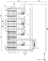
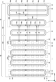
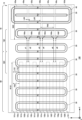
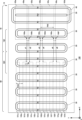
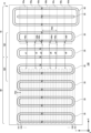
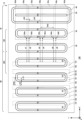
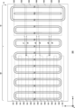
- FIG. 1 shows an example of a top view of a semiconductor device 100.
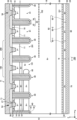
- FIG. A close-up view of an edge of an active region 110 in a top view of the semiconductor device 100 is shown.
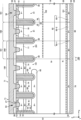
- 1B shows an example of a cross section taken along line aa' in FIG. 1B shows a modified example of the aa' cross section of FIG. 1B shows a modified example of the aa' cross section of FIG. 1 shows an example of a top view of a semiconductor device 100.
- FIG. 1 shows a modified example of the top view of the semiconductor device 100.
- 1 shows a modified example of the top view of the semiconductor device 100.
- 1 shows a modified example of the top view of the semiconductor device 100.
- 1 shows a modified example of the top view of the semiconductor device 100.
- 1 shows a modified example of the top view of the semiconductor device 100.
- FIG. 1 shows a modified example of the top view of the semiconductor device 100.
- 1 shows a modified example of the top view of the semiconductor device 100.
- 1 shows an example of a top view of a semiconductor device 500 of a comparative example.
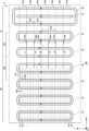
- 1 shows an example of a top view of a semiconductor device 200.
- FIG. 1 shows an example of a top view of a semiconductor device 200.
- top one side in a direction parallel to the depth direction of the semiconductor substrate is referred to as "top” and the other side as “bottom.”
- bottom one side in a direction parallel to the depth direction of the semiconductor substrate
- top surface one surface is referred to as the top surface and the other surface is referred to as the bottom surface.
- the directions of "top,” “bottom,” “front,” and “back” are not limited to the direction of gravity or the direction in which the semiconductor device is attached to a substrate or the like when mounted.
- the plane parallel to the top surface of the semiconductor substrate is referred to as the XY plane, and the orthogonal axes parallel to the top and bottom surfaces of the semiconductor substrate are referred to as the X-axis and Y-axis.
- the axis perpendicular to the top and bottom surfaces of the semiconductor substrate is referred to as the Z-axis.
- the depth direction of the semiconductor substrate may be referred to as the Z-axis.
- the case where the semiconductor substrate is viewed in the Z-axis direction is referred to as a planar view.
- the direction parallel to the top and bottom surfaces of the semiconductor substrate, including the X-axis and Y-axis may be referred to as the horizontal direction.
- the first conductivity type is N type and the second conductivity type is P type, but the first conductivity type may be P type and the second conductivity type may be N type.
- the conductivity types of the substrate, layer, region, etc. in each embodiment will be of opposite polarity.
- the conductivity type of a doped region doped with impurities is described as P type or N type.
- impurities may specifically mean either N type donors or P type acceptors, and may be described as dopants.
- doping means introducing donors or acceptors into a semiconductor substrate to make it a semiconductor that exhibits N type conductivity or a semiconductor that exhibits P type conductivity.
- doping concentration refers to the donor concentration or acceptor concentration in thermal equilibrium.
- FIG. 1A shows an example of a top view of a semiconductor device 100.
- the semiconductor device 100 is a semiconductor chip that includes a transistor portion 70 and a diode portion 80.
- the transistor section 70 includes a transistor such as an IGBT (Insulated Gate Bipolar Transistor).
- the diode section 80 includes a diode such as a free wheel diode (FWD).
- the semiconductor device 100 of this example is a reverse conducting IGBT (RC-IGBT) that has the transistor section 70 and the diode section 80 on the same chip.
- RC-IGBT reverse conducting IGBT
- the semiconductor substrate 10 may be a silicon substrate, a silicon carbide substrate, a nitride semiconductor substrate such as gallium nitride, or the like.
- the semiconductor substrate 10 is a silicon substrate.
- the semiconductor substrate 10 has an active region 110 and a peripheral region 120.
- the transistor section 70 is a region obtained by projecting a collector region 22 (described later) provided on the underside of the semiconductor substrate 10 onto the upper surface of the semiconductor substrate 10.
- the diode section 80 is a region obtained by projecting a backside region 82 (described later) provided on the underside of the semiconductor substrate 10 onto the upper surface of the semiconductor substrate 10.
- the transistor sections 70 and diode sections 80 may be arranged alternately and periodically in the XY plane.
- the transistor sections 70 and diode sections 80 each include a plurality of transistor sections and diode sections.
- a gate metal layer 50 may be provided above the semiconductor substrate 10 in the region between the transistor sections 70 and the diode sections 80.
- the transistor section 70 and the diode section 80 have trench sections that extend in the Y-axis direction.
- the transistor section 70 and the diode section 80 may also have trench sections that extend in the X-axis direction.
- the active region 110 has a transistor portion 70 and a diode portion 80.
- the active region 110 is a region where a main current flows between the upper and lower surfaces of the semiconductor substrate 10 when the semiconductor device 100 is controlled to be in the on state. In other words, it is a region where a current flows in the depth direction inside the semiconductor substrate 10 from the upper surface to the lower surface, or from the lower surface to the upper surface.
- the transistor portion 70 and the diode portion 80 are referred to as the element portion or element region, respectively.
- the region sandwiched between the two element parts is also considered to be the active region 110.
- the region in which the gate metal layer 50 is provided and sandwiched between the element parts is also included in the active region 110.
- the gate metal layer 50 is formed of a material containing metal.
- the gate metal layer 50 is formed of aluminum, an aluminum-silicon alloy, or an aluminum-silicon-copper alloy.
- the gate metal layer 50 is electrically connected to the gate conductive portion of the transistor portion 70 and supplies a gate voltage to the transistor portion 70.
- the gate metal layer 50 is provided so as to surround the outer periphery of the active region 110 in a top view.
- the gate metal layer 50 is electrically connected to the gate pad 130 provided in the outer periphery region 120.
- the gate metal layer 50 may be provided along the outer periphery edge of the semiconductor substrate 10.
- the gate metal layer 50 may have a barrier metal formed of titanium, a titanium compound, or the like under a region formed of aluminum or the like.
- the gate metal layer 50 may also be provided between the transistor portion 70 and the diode portion 80 in a top view.
- the peripheral region 120 is a region between the active region 110 and the peripheral edge of the semiconductor substrate 10 when viewed from above.
- the peripheral region 120 is provided to surround the active region 110 when viewed from above.
- One or more metal pads may be arranged in the peripheral region 120 for connecting the semiconductor device 100 to an external device with a wire or the like.
- the peripheral region 120 may have an edge termination structure.
- the edge termination structure relieves electric field concentration on the upper surface side of the semiconductor substrate 10.
- the edge termination structure has a guard ring, a field plate, a resurf, or a structure that combines these.
- the gate pad 130 is electrically connected to the gate conductive portion of the transistor portion 70 via the gate metal layer 50.
- the gate pad 130 is set to the gate potential.
- the gate pad 130 is rectangular in top view.
- FIG. 1B shows an example of a top view of the semiconductor device 100. In this example, an enlarged view of area A in FIG. 1A is shown.
- the semiconductor device 100 of this example includes a gate trench portion 40, a dummy trench portion 30, an anode region 11, an emitter region 12, a base region 14, a first contact region 15, a well region 17, and a second contact region 19 on the front surface 21 of the semiconductor substrate 10.
- the front surface 21 will be described later.
- the semiconductor device 100 of this example also includes an emitter electrode 52 and a gate metal layer 50 provided above the front surface 21 of the semiconductor substrate 10.
- the emitter electrode 52 is provided above the gate trench portion 40, the dummy trench portion 30, the anode region 11, the emitter region 12, the base region 14, the first contact region 15, the well region 17, and the second contact region 19.
- the gate metal layer 50 is provided above the gate trench portion 40 and the well region 17.
- the emitter electrode 52 is formed of a material containing metal.
- the emitter electrode 52 may be formed of the same material as the gate metal layer, or may be formed of a different material.
- the emitter electrode 52 may have a barrier metal formed of titanium, a titanium compound, or the like, below a region formed of aluminum or the like.
- the emitter electrode 52 and the gate metal layer 50 are provided separately from each other.
- the emitter electrode 52 and the gate metal layer 50 are provided above the semiconductor substrate 10 with the interlayer insulating film 38 in between.
- the interlayer insulating film 38 is omitted in FIG. 1B.
- the interlayer insulating film 38 has contact holes 54, 55, and 56 penetrating therethrough.
- the contact hole 55 connects the gate metal layer 50 to the gate conductive portion in the transistor portion 70.
- a plug made of tungsten or the like may be formed inside the contact hole 55.
- the contact hole 56 connects the emitter electrode 52 to the dummy conductive portion in the dummy trench portion 30.
- a plug made of tungsten or the like may be formed inside the contact hole 56.
- connection portion 25 electrically connects the front surface electrode, such as the emitter electrode 52 or the gate metal layer 50, to the semiconductor substrate 10.
- the connection portion 25 is provided between the gate metal layer 50 and the gate conductive portion.
- the connection portion 25 is also provided between the emitter electrode 52 and the dummy conductive portion.
- the connection portion 25 is a conductive material, such as polysilicon doped with impurities.
- the connection portion 25 is polysilicon (N+) doped with N-type impurities.
- the connection portion 25 is provided above the front surface 21 of the semiconductor substrate 10 via an insulating film, such as an oxide film.
- the gate trench portion 40 is an example of a plurality of trench portions extending in a predetermined trench extension direction on the front surface 21 side of the semiconductor substrate 10.
- the gate trench portions 40 are arranged at predetermined intervals along a predetermined arrangement direction (the X-axis direction in this example).
- the gate trench portion 40 in this example may have two extension portions 41 extending parallel to the front surface 21 of the semiconductor substrate 10 and along an extension direction perpendicular to the arrangement direction (the Y-axis direction in this example), and a connection portion 43 connecting the two extension portions 41.
- connection portion 43 is formed in a curved shape.
- the gate metal layer 50 may be connected to the gate conductive portion.
- the dummy trench portion 30 is a trench portion electrically connected to the emitter electrode 52. Like the gate trench portion 40, the dummy trench portion 30 is arranged at predetermined intervals along a predetermined arrangement direction (the X-axis direction in this example). Like the gate trench portion 40, the dummy trench portion 30 in this example may have a U-shape on the front surface 21 of the semiconductor substrate 10. That is, the dummy trench portion 30 may have two extension portions 31 extending along the extension direction and a connection portion 33 connecting the two extension portions 31.
- the transistor section 70 in this example has a structure in which two gate trench sections 40 and three dummy trench sections 30 are repeatedly arranged. That is, the transistor section 70 in this example has gate trench sections 40 and dummy trench sections 30 in a ratio of 2:3. For example, the transistor section 70 has one extension section 31 between two extension sections 41. The transistor section 70 also has two extension sections 31 adjacent to the gate trench section 40.
- the ratio of the gate trench portion 40 to the dummy trench portion 30 is not limited to this example.
- the ratio of the gate trench portion 40 to the dummy trench portion 30 may be 1:1 or 2:4.
- the transistor portion 70 may have no dummy trench portion 30 and may be entirely made up of gate trench portions 40, forming a so-called full gate structure.
- the contact holes 54 are formed above the emitter region 12, the base region 14, and the first contact region 15.
- the contact holes 54 are provided above the anode region 11 and the second contact region 19.
- the contact holes 54 are provided above the base region 14. None of the contact holes 54 are provided above the well regions 17 provided at both ends in the Y-axis direction. In this way, one or more contact holes 54 are formed in the interlayer insulating film. The one or more contact holes 54 may be provided extending in the extension direction.
- the trench contact portion 27 electrically connects the emitter electrode 52 and the semiconductor substrate 10.
- the trench contact portion 27 is provided in the contact hole 54.
- the trench contact portion 27 is provided extending in the extension direction.
- the first boundary 190 is a region provided in the transistor portion 70 and adjacent to the diode portion 80.
- the first boundary 190 may have a base region 14.
- the first boundary 190 may have neither an emitter region 12 nor a first contact region 15.
- the trench portion of the first boundary 190 is a dummy trench portion 30.
- the first boundary 190 in this example is arranged so that both ends in the X-axis direction are dummy trench portions 30.
- the second boundary portion 290 is a region provided in the diode portion 80 and adjacent to the transistor portion 70.
- the second boundary portion 290 has an anode region 11.
- the second boundary portion 290 does not have a second contact region 19.
- the trench portion of the second boundary portion 290 is a dummy trench portion 30.
- the second boundary portion 290 is arranged so that both ends in the X-axis direction are dummy trench portions 30.
- Mesa portion 71, mesa portion 81, mesa portion 191, and mesa portion 291 are mesa portions provided adjacent to trench portions in a plane parallel to front surface 21 of semiconductor substrate 10.
- a mesa portion is a portion of semiconductor substrate 10 sandwiched between two adjacent trench portions, and may be a portion from front surface 21 of semiconductor substrate 10 to the deepest bottom of each trench portion.
- the extension portion of each trench portion may be considered as one trench portion. In other words, the area sandwiched between two extension portions may be considered as a mesa portion.
- the mesa portion 71 is provided in the transistor portion 70 adjacent to at least one of the dummy trench portion 30 or the gate trench portion 40.
- the mesa portion 71 has a well region 17, an emitter region 12, a base region 14, and a first contact region 15 on the front surface 21 of the semiconductor substrate 10.
- the emitter regions 12 and the first contact regions 15 are provided alternately in the extension direction.
- the mesa portion 81 is provided in a region of the diode portion 80 that is sandwiched between adjacent dummy trench portions 30.
- the mesa portion 81 has a second contact region 19 on the front surface 21 of the semiconductor substrate 10.
- the mesa portion 81 has a base region 14 and a well region 17 on the negative side in the Y-axis direction.
- the mesa portion 191 is provided in the first boundary portion 190.
- the mesa portion 191 has a base region 14 on the front surface 21 of the semiconductor substrate 10.
- the mesa portion 191 has a base region 14 and a well region 17 on the negative side in the Y-axis direction.
- the mesa portion 291 is provided in the second boundary portion 290.
- the mesa portion 291 has an anode region 11 on the front surface 21 of the semiconductor substrate 10.
- the mesa portion 291 has a base region 14 and a well region 17 on the negative side in the Y-axis direction.
- the anode region 11 is a region of a second conductivity type provided on the front surface 21 side of the semiconductor substrate 10 in the diode section 80.
- the anode region 11 is, for example, a P-type.
- the anode region 11 may be formed with the same dopant as the base region 14, or may be formed with a different dopant.
- the doping concentration of the anode region 11 may be the same as the doping concentration of the base region 14, or may be different.
- the base region 14 is a second conductivity type region provided on the front surface 21 side of the semiconductor substrate 10 in the transistor portion 70 and the diode portion 80.
- the base region 14 is P-type, for example.
- the base region 14 may be provided on both ends in the Y-axis direction of the mesa portion 71, the mesa portion 81, the mesa portion 191, and the mesa portion 291 on the front surface 21 of the semiconductor substrate 10. Note that FIG. 1B shows only one end of the base region 14 in the Y-axis direction.
- the emitter region 12 is a region of the first conductivity type having a higher doping concentration than the drift region 18.
- the emitter region 12 is, for example, N+ type.
- One example of a dopant for the emitter region 12 is arsenic (As).
- the emitter region 12 is provided in contact with the gate trench portion 40 on the front surface 21 of the mesa portion 71.
- the emitter region 12 may be provided extending in the X-axis direction from one of the two trench portions sandwiching the mesa portion 71 to the other.
- the emitter region 12 is also provided below the contact hole 54.
- the first contact region 15 is a region of a second conductivity type having a higher doping concentration than the base region 14.
- the first contact region 15 is a P+ type, for example.
- the first contact region 15 is provided on the front surface 21 of the mesa portion 71.
- the first contact region 15 may be provided in the X-axis direction from one of the two trench portions sandwiching the mesa portion 71 to the other.
- the first contact region 15 may or may not be in contact with the gate trench portion 40.
- the first contact region 15 may or may not be in contact with the dummy trench portion 30.
- the first contact region 15 is in contact with the dummy trench portion 30 and the gate trench portion 40.
- the first contact region 15 may also be provided below the contact hole 54.
- the second contact region 19 is a region of a second conductivity type having a higher doping concentration than the anode region 11.
- the second contact region 19 is P-type, for example.
- the doping concentration of the second contact region 19 may be the same as or different from the doping concentration of the first contact region 15.
- the doping concentration of the second contact region 19 in this example is lower than the doping concentration of the first contact region 15.
- the second contact region 19 in this example is provided on the front surface 21 of the mesa portion 81.
- the second contact region 19 may be provided in the X-axis direction from one of the two trench portions sandwiching the mesa portion 81 to the other.
- the second contact region 19 may or may not be in contact with the dummy trench portion 30.
- the second contact region 19 is in contact with the dummy trench portion 30.
- the second contact region 19 may also be provided below the contact hole 54.
- FIG. 1C is a diagram showing an example of the a-a' cross section in FIG. 1B.
- the a-a' cross section is an XZ plane passing through the emitter region 12 in the transistor section 70.
- the semiconductor device 100 of this example has a semiconductor substrate 10 including an accumulation region 16 and a trench bottom region 65, an interlayer insulating film 38, an emitter electrode 52, and a collector electrode 24.
- the emitter electrode 52 is formed above the semiconductor substrate 10 and the interlayer insulating film 38.
- the drift region 18 is a region of a first conductivity type provided in the semiconductor substrate 10.
- the drift region 18 is, as an example, N-type.
- the drift region 18 may be a region remaining in the semiconductor substrate 10 without other doped regions being formed therein.
- the doping concentration of the drift region 18 may be the doping concentration of the semiconductor substrate 10.
- the buffer region 20 is a region of a first conductivity type provided below the drift region 18.
- the buffer region 20 is, as an example, an N-type.
- the doping concentration of the buffer region 20 is higher than the doping concentration of the drift region 18.
- the buffer region 20 may function as a field stop layer that prevents the depletion layer spreading from the lower surface side of the base region 14 from reaching the collector region 22 of the second conductivity type and the back side region 82 of the first conductivity type.
- the collector region 22 is provided below the drift region 18 in the transistor portion 70.
- the collector region 22 has the second conductivity type.
- the collector region 22 is a P+ type.
- the back side region 82 is provided below the drift region 18 in the diode section 80.
- the back side region 82 has a first conductivity type section 82-1 and a second conductivity type section 82-2.
- the boundary between the collector region 22 and the back side region 82 is the boundary between the transistor section 70 and the diode section 80.
- the first conductivity type portion 82-1 is a region of the first conductivity type having a higher doping concentration than the drift region 18.
- the first conductivity type portion 82-1 of this example is provided in contact with the rear surface 23 of the semiconductor substrate 10.
- the doping concentration of the first conductivity type portion 82-1 may be higher than the doping concentration of the buffer region 20.
- the doping concentration of the first conductivity type portion 82-1 may be 1E15 cm -3 or more and 1E21 cm -3 or less.
- the first conductivity type portion 82-1 is N+ type.
- the second conductivity type portion 82-2 is a region of the second conductivity type having a higher doping concentration than the base region 14.
- the doping concentration of the second conductivity type portion 82-2 may be 1E16 cm -3 or more and 1E21 cm -3 or less.
- the second conductivity type portion 82-2 is P+ type.
- the doping concentration of the second conductivity type portion 82-2 may be the same as or different from the doping concentration of the collector region 22.
- the second conductivity type portion 82-2 of this example is in contact with the rear surface 23 of the semiconductor substrate 10 and is provided adjacent to the first conductivity type portion 82-1.
- the second conductivity type portion 82-2 may be in direct contact with the first conductivity type portion 82-1.
- the first conductivity type section 82-1 may be formed by ion implanting a P-type dopant and then further injecting an N-type dopant in the ion implantation process for forming the second conductivity type section 82-2.
- the second conductivity type section 82-2 may be formed by ion implanting an N-type dopant and then further injecting a P-type dopant in the ion implantation process for forming the first conductivity type section 82-1.
- the first conductivity type portion 82-1 and the second conductivity type portion 82-2 are provided to form a repeating structure in which the second conductivity type non-forming region 181 and the second conductivity type forming region 182 are alternately and repeatedly arranged in a predetermined direction.
- the second conductivity type non-forming region 181 is a region in which the second conductivity type portion 82-2 is not formed on the rear surface 23 side of the semiconductor substrate 10 when viewed from above.
- the second conductivity type forming region 182 is a region in which the second conductivity type portion 82-2 is formed on the rear surface 23 side of the semiconductor substrate 10 when viewed from above.
- the second-conductivity-type non-forming regions 181 and the second-conductivity-type forming regions 182 may be arranged alternately in the trench arrangement direction (e.g., the X-axis direction) or alternately in the trench extension direction (e.g., the Y-axis direction).
- the second-conductivity-type non-forming regions 181 and the second-conductivity-type forming regions 182 may be arranged in a striped pattern when viewed from above. This makes it possible to reduce the forward voltage Vf of the diode section 80.
- the arrangement of the second-conductivity-type non-forming regions 181 and the second-conductivity-type forming regions 182 will be described in detail later.
- the rear surface 23 of the semiconductor substrate 10 has a first conductivity type portion 82-1.
- the current during switching of the semiconductor device 100 is made uniform, improving the switching efficiency.
- the collector electrode 24 is formed on the rear surface 23 of the semiconductor substrate 10.
- the collector electrode 24 is formed of a conductive material such as a metal.
- the material of the collector electrode 24 may be the same as or different from the material of the emitter electrode 52 and the gate metal layer 50.
- the accumulation region 16 is a region of a first conductivity type that is provided closer to the front surface 21 of the semiconductor substrate 10 than the drift region 18.
- the accumulation region 16 is an N+ type, for example.
- the accumulation region 16 is provided in the transistor section 70. However, the accumulation region 16 does not necessarily have to be provided.
- the accumulation region 16 is provided in contact with the gate trench portion 40.
- the accumulation region 16 may or may not be in contact with the dummy trench portion 30.
- the doping concentration of the accumulation region 16 is higher than the doping concentration of the drift region 18.
- the interlayer insulating film 38 is provided on the front surface 21.
- An emitter electrode 52 is provided above the interlayer insulating film 38.
- One or more contact holes 54 are provided in the interlayer insulating film 38 to electrically connect the emitter electrode 52 to the semiconductor substrate 10.
- Contact holes 55 and 56 may also be provided penetrating the interlayer insulating film 38.
- the trench contact portion 27 has a conductive material filled in the contact hole 54.
- the trench contact portion 27 is provided between two adjacent trench portions among the multiple trench portions.
- the trench contact portion 27 is provided penetrating the emitter region 12 from the front surface 21.
- the trench contact portion 27 may have the same material as the emitter electrode 52.
- the bottom end of the trench contact portion 27 is deeper than the bottom end of the emitter region 12.
- the resistance of the base region 14 is reduced, making it easier to extract minority carriers (e.g., holes). This improves the breakdown resistance, such as the latch-up resistance, caused by minority carriers.
- the trench contact portion 27 has a bottom surface that is substantially planar.
- the bottom surface of the trench contact portion 27 may be covered with a plug layer of the second conductivity type or the like.
- the trench contact portion 27 has a tapered shape with inclined sidewalls.
- the sidewalls of the trench contact portion 27 may be provided substantially perpendicular to the front surface 21.
- One or more gate trench portions 40 and one or more dummy trench portions 30 are provided on the front surface 21.
- Each trench portion is provided from the front surface 21 to the drift region 18.
- each trench portion also penetrates these regions to reach the drift region 18.
- the trench portion penetrating the doping region is not limited to being manufactured in the order of forming the doping region and then the trench portion.
- the trench portion penetrating the doping region also includes a trench portion formed after the trench portion is formed.
- the gate trench portion 40 has a gate trench, a gate insulating film 42, and a gate conductive portion 44 formed on the front surface 21.
- the gate insulating film 42 is formed to cover the inner wall of the gate trench.
- the gate insulating film 42 may be formed by oxidizing or nitriding the semiconductor on the inner wall of the gate trench.
- the gate conductive portion 44 is formed inside the gate trench, further inside than the gate insulating film 42.
- the gate insulating film 42 insulates the gate conductive portion 44 from the semiconductor substrate 10.
- the gate conductive portion 44 is formed of a conductive material such as polysilicon.
- the gate trench portion 40 is covered by an interlayer insulating film 38 on the front surface 21.
- the gate conductive portion 44 includes a region facing the adjacent base region 14 on the mesa portion 71 side across the gate insulating film 42 in the depth direction of the semiconductor substrate 10. When a predetermined voltage is applied to the gate conductive portion 44, a channel is formed by an electron inversion layer on the surface layer of the interface of the base region 14 that contacts the gate trench.
- the dummy trench portion 30 may have the same structure as the gate trench portion 40.
- the dummy trench portion 30 has a dummy trench, a dummy insulating film 32, and a dummy conductive portion 34 formed on the front surface 21 side.
- the dummy insulating film 32 is formed to cover the inner wall of the dummy trench.
- the dummy conductive portion 34 is formed inside the dummy trench and is formed further inward than the dummy insulating film 32.
- the dummy insulating film 32 insulates the dummy conductive portion 34 from the semiconductor substrate 10.
- the dummy trench portion 30 is covered by an interlayer insulating film 38 on the front surface 21.
- the trench bottom region 65 is a region of a second conductivity type provided below the base region 14.
- the doping concentration of the trench bottom region 65 in this example is higher than the doping concentration of the base region 14.
- the trench bottom region 65 in this example is, for example, a P+ type.
- the doping concentration of the trench bottom region 65 may be 1E14 cm ⁇ 3 or more and 1E18 cm ⁇ 3 or less.
- the trench bottom region 65 in this example is provided so that its upper end does not contact the accumulation region 16. That is, in the depth direction of the semiconductor substrate 10, the drift region 18 is formed between the trench bottom region 65 and the accumulation region 16.
- the trench bottom region 65 may be provided so that its upper end contacts the lower end of the accumulation region 16.
- the trench bottom region 65 in this example is provided so as to extend from the lower end of one of the multiple trench portions to the lower end of the other opposing trench portion in the trench arrangement direction of the multiple trench portions.
- the trench bottom region 65 may be provided so as to extend from the lower end of one of the multiple trench portions beyond the lower end of the other opposing trench portion to the lower end of the trench portion adjacent to the other opposing trench portion.
- the trench bottom region 65 may be provided so as to extend beyond the lower ends of two or more multiple trench portions.
- the first lifetime control region 151 is provided in the diode section 80. This allows the semiconductor device 100 of this example to speed up recovery in the diode section 80 and reduce switching losses.
- the first lifetime control region 151 may also be provided in the transistor section 70.
- the first lifetime control region 151 may be formed by injecting impurities from the front surface 21 side, or from the back surface 23 side.
- the first lifetime control region 151 may be formed by ion implantation of helium into the semiconductor substrate 10.
- the second lifetime control region 152 is provided on the front surface 21 side of the center of the semiconductor substrate 10 in the depth direction of the semiconductor substrate 10.
- the second lifetime control region 152 is provided in the drift region 18.
- the second lifetime control region 152 is provided in both the transistor section 70 and the diode section 80.
- the second lifetime control region 152 may be formed by injecting impurities from the front surface 21 side, or may be formed by injecting impurities from the back surface 23 side.
- the second lifetime control region 152 is provided in the diode section 80, the first boundary section 190, and the second boundary section 290, and may not be provided in a part of the transistor section 70.
- the second lifetime control region 152 may be formed by any of the methods for forming the first lifetime control region 151.
- the elements and dose amounts used to form the first lifetime control region 151 and the second lifetime control region 152 may be the same or different.
- FIG. 1D is a diagram showing a modified example of the a-a' cross section in FIG. 1B. The differences from FIG. 1C will be explained using FIG. 1D.
- the first conductivity type portion 82-1 is provided on the rear surface 23 of the semiconductor substrate 10.
- the first conductivity type portion 82-1 may function as the cathode of the diode portion 80.
- the second conductivity type section 82-2 is provided above the first conductivity type section 82-1.
- the second conductivity type section 82-2 is provided in contact with the first conductivity type section 82-1, but this is not limited to this.
- the second conductivity type section 82-2 may be provided spaced apart from the first conductivity type section 82-1.
- the second conductivity type portion 82-2 has the same thickness as the first conductivity type portion 82-1.
- the second conductivity type portion 82-2 may be thinner than the first conductivity type portion 82-1.
- the second conductivity type portion 82-2 may have a thickness equal to or less than the length from the upper end of the first conductivity type portion 82-1 to the lower end of the first lifetime control region 151.
- the second conductivity type portion 82-2 in this example is provided closer to the back surface 23 of the semiconductor substrate 10 than the first lifetime control region 151.
- the second conductivity type portion 82-2 may also be provided closer to the front surface 21 of the semiconductor substrate 10 than the first lifetime control region 151.
- the second-conductivity-type non-forming region 181 is a region in which the second-conductivity-type portion 82-2 is not formed on the rear surface 23 side of the semiconductor substrate 10 when viewed from above.
- the second-conductivity-type forming region 182 is a region in which the second-conductivity-type portion 82-2 is formed on the rear surface 23 side of the semiconductor substrate 10 when viewed from above. Even when the second-conductivity-type portion 82-2 is formed above the first-conductivity-type portion 82-1 as in this example, a repeating structure can be formed in which the second-conductivity-type non-forming region 181 and the second-conductivity-type forming region 182 are alternately and repeatedly arranged when viewed from above.
- FIG. 1E is a diagram showing a modified example of the a-a' cross section in FIG. 1B. The differences from FIG. 1C will be explained using FIG. 1E.
- the depth position of the lower end of the trench bottom region 65 is located closer to the front surface 21 than the depth positions of the trench bottoms of the multiple trench portions.
- the depth position of the upper end of the trench bottom region 65 is located deeper than the base region 14.
- the depth position of the upper end of the trench bottom region 65 may be located deeper than the accumulation region 16.
- a drift region 18 may be provided between the trench bottom region 65 and the accumulation region 16.
- the trench bottom region 65 is provided such that the depth position of the bottom end is shallower than the depth positions of the bottom ends of the gate trench portion 40 and the dummy trench portion 30. In other words, the trench bottom region 65 does not need to cover the trench bottoms of the gate trench portion 40 and the dummy trench portion 30. Even in such a case, it is possible to increase the gate capacitance of the transistor portion 70 and reduce the on-loss Eon of the semiconductor device 100.
- FIG. 2A shows an example of a top view of the semiconductor device 100.
- the positional relationship between the trench bottom region 65, the second conductivity type non-forming region 181, and the second conductivity type forming region 182 in the semiconductor device 100 of this example will be explained.
- the configuration necessary for explanation is shown, and other configurations are omitted.
- the transistor section 70 has a plurality of trench bottom regions 65 repeatedly arranged in the trench extension direction of the plurality of trench sections (the Y-axis direction in this example).
- the transistor section 70 has a plurality of trench bottomless regions 66 repeatedly arranged in the trench extension direction and sandwiched between the plurality of trench bottom regions 65.
- the trench bottom regions 65 and the trench bottomless regions 66 extend from the transistor section 70 toward the diode section 80 in the trench arrangement direction, but do not reach the diode section 80 and terminate at the first boundary section 190.
- the width W65 of the trench bottom region 65 in the trench arrangement direction may be the same as the width of the transistor section 70 in the trench arrangement direction, or may be smaller than the width of the transistor section 70 in the trench arrangement direction.
- the trench bottom region 65 may be provided extending from one end to the other end of the transistor section 70 in the trench arrangement direction.
- the multiple trench bottom regions 65 are repeatedly arranged at a predetermined trench bottom repetition period P65.
- the trench bottom repetition period P65 may be the distance from one end of one trench bottom region 65 in the trench extension direction, beyond the other end of the trench bottom region, to an adjacent trench bottom region 65.
- the trench bottom repetition period P65 is the distance from the Y-axis negative end edge of trench bottom region 65b to the Y-axis negative end edge of trench bottom region 65c.
- the trench bottom repeat period P65 is greater than the back side repeat period P82 described below.
- the trench bottom repeat period P65 may be an integer multiple of the back side repeat period P82.
- the trench bottom repeat period P65 is 5 ⁇ m or more and 200 ⁇ m or less.
- the area of the trench bottom region 65 is larger than the area of the trench bottomless region 66.
- the width L65 of the trench bottom region 65 in the trench extension direction is larger than the width L66 of the trench bottomless region 66 in the trench extension direction.
- the width L65 of the trench bottom region 65 in the trench extension direction is 1 to 10 times the width L66 of the trench bottomless region 66.
- the width L65 of the trench bottom region 65 in the trench extension direction may be larger than the width L181 of the second conductivity type non-forming region 181 in the trench extension direction, and may be larger than the width L182 of the second conductivity type forming region 182 in the trench extension direction.
- the areas of the multiple trench bottomless regions 66 sandwiched between the multiple trench bottom regions 65 may be approximately the same. In one example, the areas of the multiple trench bottomless regions 66 sandwiched between the multiple trench bottom regions 65 are each 85% or more and 115% or less of a predetermined reference value. As one example, the area of the trench bottomless region 66a in a top view is the same as the area of the trench bottomless region 66b.
- the predetermined reference value may be the area of any one of the areas of the multiple trench bottomless regions 66.
- the predetermined reference value may be the average value, the minimum value, or the maximum value of the areas of the multiple trench bottomless regions 66.
- the diode section 80 is provided with a second-conductivity-type non-forming region 181 and a second-conductivity-type forming region 182.
- the second-conductivity-type non-forming region 181 and the second-conductivity-type forming region 182 extend in the trench arrangement direction (the X-axis direction in this example) and are arranged alternately in the trench extension direction.
- the second-conductivity-type non-forming region 181 and the second-conductivity-type forming region 182 extend from the diode section 80 toward the transistor section 70 in the trench arrangement direction, but do not reach the transistor section 70 and terminate at the second boundary section 290.
- the width W181 of the second-conductivity-type non-forming region 181 in the trench arrangement direction may be the same as the width of the diode section 80 in the trench arrangement direction, or may be smaller than the width of the diode section 80 in the trench arrangement direction.
- the second-conductivity-type non-forming region 181 may be provided extending from one end to the other end of the diode section 80 in the trench arrangement direction.
- the second-conductivity-type non-forming regions 181 and the second-conductivity-type forming regions 182 are alternately arranged at a predetermined back-side repetition period P82.
- the back-side repetition period P82 may be the distance from one end of one second-conductivity-type non-forming region 181 in the trench extension direction, beyond the other end of the second-conductivity-type non-forming region 181, to the adjacent second-conductivity-type non-forming region 181.
- the back-side repetition period P82 is the distance from the end edge on the Y-axis positive side of the second-conductivity-type non-forming region 181a to the end edge on the Y-axis positive side of the second-conductivity-type non-forming region 181b.
- the back side repetition period P82 is smaller than the trench bottom repetition period P65.
- the back side repetition period P82 may be 20 ⁇ m, 30 ⁇ m, or 50 ⁇ m. In one example, the back side repetition period P82 is 10 ⁇ m or more and 100 ⁇ m or less.
- the second-conductivity-type non-forming regions 181 and the second-conductivity-type forming regions 182 may be arranged alternately in the trench extension direction, or may be arranged alternately in the trench arrangement direction.
- the second-conductivity-type non-forming regions 181 and the second-conductivity-type forming regions 182 extend in the trench arrangement direction and are arranged alternately in the trench extension direction.
- the area of the second conductivity type non-forming region 181 and the area of the second conductivity type forming region 182 are the same.
- the area of the second conductivity type non-forming region 181a and the area of the second conductivity type forming region 182a are the same.
- the areas of the second conductivity type non-forming region 181 and the second conductivity type forming region 182 may be different.
- the width L181 of the second conductivity type non-forming region 181 in the trench extension direction may be different from the width L182 of the second conductivity type forming region in the trench extension direction.
- the width L181 of the second conductivity type non-forming region 181 in the trench extension direction is 30% or more and 70% or less of the sum of the width L181 of the second conductivity type non-forming region 181 and the width L182 of the second conductivity type forming region 182 in the trench extension direction.
- the area of the second conductivity type non-forming region 181 may be 30% or more and 70% or less of the area of the back side region 82.
- each end 166 of the multiple trench bottomless regions 66 is 85% or more and 115% or less of a predetermined reference value.
- each end 166 of the multiple trench bottomless regions 66 is a corner of the trench bottomless region 66.
- the predetermined reference value may be the shortest distance from any one of the multiple ends 166 to the second-conductivity-type non-forming region 181.
- the predetermined reference value may be the average value, minimum value, or maximum value of the shortest distances from each of the multiple ends 166 to the second-conductivity-type non-forming region 181.
- the shortest distance from the end 166a on the positive side of the Y axis of the trench bottomless region 66a to the second-conductivity-type non-forming region 181c is indicated as d1.
- d2 to d6 are the shortest distances from the end 166b of the trench bottomless region 66a, the end 166c and the end 166d of the trench bottomless region 66b, and the end 166e and the end 166f of the trench bottomless region 66c to the second-conductivity-type non-forming region 181.
- the shortest distances d1 to d6 from the end 166 of each of the multiple trench bottomless regions 66 to the multiple second-conductivity-type non-forming regions 181 are all approximately the same.
- the distance from each end 166 of each trench bottomless region 66 to the second-conductivity-type non-forming region 181 is uniformed. This makes it possible to uniform the electronic current flowing when the semiconductor device 100 is switched on, thereby reducing the on-loss Eon.
- each of the multiple trench bottomless regions 66 faces one of the multiple second-conductivity-type non-forming regions 181.
- trench bottomless region 66a faces second-conductivity-type non-forming region 181c
- trench bottomless region 66b faces second-conductivity-type non-forming region 181e
- trench bottomless region 66c faces second-conductivity-type non-forming region 181g.
- FIG. 2B shows a modified top view of the semiconductor device 100. Differences from FIG. 2A will be explained using FIG. 2B.
- the trench bottom repeat period P65 is the same as in the example shown in FIG. 2A.
- the width L65 of the trench bottom region is smaller than in the example shown in FIG. 2A, and the width L66 of the trench bottomless region is larger than in the example shown in FIG. 2A.
- the area occupied by the trench bottomless region 66 in one trench bottom repeat period P65 is larger than in the example shown in FIG. 2A.
- the width L181 of the second-conductivity-type non-forming region 181 and the width L182 of the second-conductivity-type forming region 182 are smaller than those in the example shown in FIG. 2A.
- the back-surface-side repetition period P82 is smaller than that in the example shown in FIG. 2A.
- each of the multiple trench bottomless regions 66 faces two or more of the multiple second-conductivity-type non-forming regions 181 in the trench arrangement direction of the multiple trench portions.
- a total of three second-conductivity-type non-forming regions 181 are provided to face one trench bottomless region 66: one second-conductivity-type non-forming region 181 having the same center line as one trench bottomless region 66, and two second-conductivity-type non-forming regions 181 provided line-symmetrically on both sides of the center line of the second-conductivity-type non-forming region 181.
- the shortest distances d1 to d6 from the respective ends 166 of the multiple trench bottomless regions 66 to the second-conductivity-type non-forming regions 181 are all approximately the same. This allows the electron current from the trench bottomless region 66 to be uniformly distributed, thereby reducing the on-loss Eon of the semiconductor device 100.
- the number of second-conductivity-type non-forming regions 181 facing one trench bottomless region 66 is not limited to this example.
- One trench bottomless region 66 may face two second-conductivity-type non-forming regions 181, or may face four or more second-conductivity-type non-forming regions 181.
- FIG. 2C shows a modified top view of the semiconductor device 100. Differences from FIG. 2A will be explained using FIG. 2C.
- the second-conductivity-type non-forming region 181 in this example has a predetermined length L181x in the trench arrangement direction of the multiple trench portions (X direction in this example), and a predetermined width L181y in the trench extension direction of the multiple trench portions (Y direction in this example).
- the length L181x and the width L181y may be approximately the same, so that the second-conductivity-type non-forming region 181 may be provided in an approximately square shape when viewed from above.
- the length L181x and the width L181y may be different.
- the second-conductivity-type non-forming regions 181 and the second-conductivity-type forming regions 182 are arranged alternately and repeatedly in two directions.
- the second-conductivity-type non-forming regions 181 and the second-conductivity-type forming regions 182 may have an arrangement direction period P82x in the trench arrangement direction of the multiple trench portions (in this example, the X direction) and an extension direction period P82y in the trench extension direction of the multiple trench portions (in this example, the Y direction).
- the arrangement direction period P82x and the extension direction period P82y may be substantially the same, whereby the second-conductivity-type non-forming regions 181 and the second-conductivity-type forming regions 182 may be arranged in a dot shape in a top view. Even in such a case, the distance from each end 166 of each trench bottomless region 66 to the second-conductivity-type non-forming region 181 can be made uniform, thereby reducing the on-loss Eon.
- the arrangement direction period P82x and the extension direction period P82y may be different.
- FIG. 2D shows a modified top view of the semiconductor device 100.
- FIG. 2D is an example of a top view in which the depth positions of the lower ends of the multiple trench bottom regions 65 are located closer to the front surface 21 of the semiconductor substrate 10 than the depth positions of the trench bottoms of the multiple trench portions, as in FIG. 1E.
- the trench bottom regions 65 do not cover the trench bottoms of the trench portions. Therefore, in a top view, the trench bottom regions 65 are provided only in the mesa portion of the transistor portion 70.
- the electron current also flows through the trench bottomless region 66, so that the distance from each end 166 of each trench bottomless region 66 to the second conductivity type non-forming region 181 can be made uniform, as in the cases described in FIG. 2A to FIG. 2C, and the on-loss Eon can be reduced.
- FIG. 3A shows a modified top view of the semiconductor device 100.
- the trench bottom repeat period P65 and the back side repeat period P82 are the same as those in the example of FIG. 2A.
- the example of FIG. 3A differs from the example of FIG. 2A in that the trench bottomless region 66 faces the second conductivity type forming region 182 in the trench arrangement direction.
- each of the multiple trench bottomless regions 66 may face one of the multiple second conductivity type forming regions 182. In other words, in the trench arrangement direction, each of the multiple trench bottomless regions 66 does not have to face one of the multiple second conductivity type non-forming regions 181.
- the trench bottomless region 66a faces the second conductivity type forming region 182a
- the trench bottomless region 66b faces the second conductivity type forming region 182c
- the trench bottomless region 66c faces the second conductivity type forming region 182e
- the trench bottomless region 66d faces the second conductivity type forming region 182g.
- the shortest distances d1 to d6 from the ends 166 of the trench bottomless regions 66 to the second-conductivity-type non-forming regions 181 are all substantially the same, as in the example shown in FIG. 2A. Therefore, the length of the path through which the electron current flows when the semiconductor device 100 is switched on can be made uniform in each trench bottomless region 66, thereby reducing the on-loss Eon.
- the distance W indicates the offset width between the end 166 of the trench bottomless region 66 in the trench extension direction and the second-conductivity-type non-forming region 181 in a top view.
- the end 166 does not face the second-conductivity-type non-forming region 181, so the distance W is greater than 0.
- the distance W may be greater than 0 and less than or equal to 50% of the width of the trench bottom region 65 in the trench extension direction.
- FIG. 3B shows a modified top view of the semiconductor device 100. Differences from FIG. 2B will be explained using FIG. 3B.
- each of the trench bottomless regions 66 may face two or more of the second conductivity type forming regions 182.
- a total of three second conductivity type forming regions 182 are provided to face one trench bottomless region 66, including one second conductivity type forming region 182 having the same center line as one trench bottomless region 66 and two second conductivity type forming regions 182 provided line-symmetrically on both sides of the second conductivity type forming region 182 across the center line.
- the shortest distances d1 to d6 from the respective ends 166 of the trench bottomless regions 66 to the second conductivity type non-forming region 181 are all approximately the same.
- the electron current from the trench bottomless region 66 is uniformly distributed, thereby reducing the on-loss Eon of the semiconductor device 100.
- FIG. 4 shows a modified top view of the semiconductor device 100. Differences from FIG. 2A will be explained using FIG. 4.
- the second-conductivity-type non-forming regions 181 and the second-conductivity-type forming regions 182 extend in the trench extension direction and are arranged alternately in the trench arrangement direction.
- the second-conductivity-type non-forming regions 181 are provided perpendicular to the arrangement direction of the multiple trench bottomless regions 66, so that the shortest distances d1 to d6 from the ends 166 of the multiple trench bottomless regions 66 to the second-conductivity-type non-forming regions 181 are all the same. This allows the electron current from the trench bottomless regions 66 to be uniformly distributed, thereby reducing the on-loss Eon of the semiconductor device 100.
- FIG. 5 shows an example of a top view of a semiconductor device 500 of the comparative example.
- the semiconductor device 500 of the comparative example has a plurality of trench bottom regions 565 repeatedly provided in the trench extension direction of a plurality of trench portions, and a plurality of trench bottomless regions 566 repeatedly provided in the trench extension direction and sandwiched between the plurality of trench bottom regions 565.
- the semiconductor device 500 of the comparative example has second-conductivity-type non-forming regions 581 and second-conductivity-type forming regions 582 extending in the trench arrangement direction and arranged alternately in the trench extension direction.
- the semiconductor device 500 of the comparative example there is no restriction between the position where the trench bottomless region 566 is provided and the position where the second-conductivity-type non-forming region 581 is provided.
- the second-conductivity-type non-forming region 581 and the second-conductivity-type forming region 582 are not provided in line symmetry with respect to the center line of one trench bottomless region 566.
- the semiconductor device 500 of the comparative example there is no restriction between the position where the trench bottomless region 566 is provided and the position where the second conductivity type non-forming region 581 is provided, so the shortest distance from the end of each trench bottomless region 566 to the second conductivity type non-forming region 581 varies for each trench bottomless region 566. That is, in the semiconductor device 500 of the comparative example, the shortest distances d1 to d6 are not approximately the same.
- the shortest distance from each end of the multiple trench bottomless regions to the second conductivity type non-forming region can be made uniform.
- the shortest distances d1 to d6 from each end of the multiple trench bottomless regions to the second conductivity type non-forming region can all be made approximately the same.
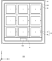
- FIG. 6A shows an example of a top view of the semiconductor device 200.
- the semiconductor device 200 is a semiconductor chip having a transistor portion 70 and a diode portion 80.
- the semiconductor device 200 differs from the semiconductor device 100 in the shapes of the transistor section 70 and the diode section 80.
- the diode section 80 is provided so as to surround the outer periphery of the transistor section 70.
- the semiconductor device 200 may include a plurality of unit structures in which the outer periphery of the transistor section 70 is surrounded by the diode section 80.
- the semiconductor device 200 includes a total of nine unit structures, with the unit structure being repeated three times in each of the X-axis direction and the Y-axis direction.
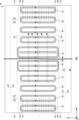
- FIG. 6B shows an example of a top view of the semiconductor device 200. In this example, an enlarged view of region B in FIG. 6A is shown.
- the transistor section 70 has multiple trench sections including the gate trench section 40 and the dummy trench section 30.
- the diode section 80 has multiple trench sections including the dummy trench section 30. Note that the diode section 80 does not necessarily have to have a trench section.
- the transistor section 70 has a plurality of trench bottom regions 65 repeatedly arranged in the trench extension direction of the plurality of trench sections (the Y-axis direction in this example).
- the transistor section 70 has a plurality of trench bottomless regions 66 repeatedly arranged in the trench extension direction and sandwiched between the plurality of trench bottom regions 65.
- the trench bottom regions 65 and the trench bottomless regions 66 extend from the transistor section 70 toward the diode section 80 in the trench arrangement direction, and terminate without reaching the diode section 80.
- the diode section 80 of this example has second-conductivity-type non-forming regions 181 and second-conductivity-type forming regions 182 that are alternately arranged in the trench extension direction of the multiple trench sections in a region facing the multiple trench bottomless regions 66. This makes it possible to equalize the electronic current that flows when the semiconductor device 200 is switched on, and reduce the on-loss Eon, even when the diode section 80 surrounds the outer periphery of the transistor section 70.
- the diode section 80 may not have a second-conductivity-type forming region 182 in a region that does not face the multiple trench bottomless regions 66.
- the second-conductivity-type forming region 182 is not provided in the diode section 80 adjacent to the transistor section 70 in the trench extension direction of the multiple trench sections.
- the trench bottom of the gate trench section 40 in the trench extension direction is covered with the trench bottom region 65, so that no electronic current flows. Therefore, in a region that does not face the multiple trench bottomless regions 66, the on-loss Eon of the semiconductor device 200 is not affected even if the second-conductivity-type non-forming region 181 and the second-conductivity-type forming region 182 are not arranged alternately.
- 10 semiconductor substrate, 11: anode region, 12: emitter region, 14: base region, 15: first contact region, 16: accumulation region, 17: well region, 18: drift region, 19: second contact region, 20: buffer region, 21: front surface, 22: collector region, 23: back surface, 24: collector electrode, 25: connection portion, 27: trench contact portion, 30: dummy trench portion, 31: extension portion, 32: dummy insulating film, 33: connection portion, 34: dummy conductive portion, 38: interlayer insulating film, 40: gate trench portion, 41: extension portion, 42: gate insulating film, 43: connection portion, 44: gate conductive portion, 50: gate metal layer, 52: emitter electrode, 54: contact hole, 55: contact hole, 56: contact hole 1.
Landscapes
- Metal-Oxide And Bipolar Metal-Oxide Semiconductor Integrated Circuits (AREA)
- Electrodes Of Semiconductors (AREA)
Priority Applications (3)
| Application Number | Priority Date | Filing Date | Title |
|---|---|---|---|
| CN202480028407.7A CN121040233A (zh) | 2023-11-29 | 2024-10-08 | 半导体装置 |
| JP2025560872A JPWO2025115409A1 (cg-RX-API-DMAC7.html) | 2023-11-29 | 2024-10-08 | |
| US19/369,284 US20260052756A1 (en) | 2023-11-29 | 2025-10-26 | Semiconductor device |
Applications Claiming Priority (2)
| Application Number | Priority Date | Filing Date | Title |
|---|---|---|---|
| JP2023-201405 | 2023-11-29 | ||
| JP2023201405 | 2023-11-29 |
Related Child Applications (1)
| Application Number | Title | Priority Date | Filing Date |
|---|---|---|---|
| US19/369,284 Continuation US20260052756A1 (en) | 2023-11-29 | 2025-10-26 | Semiconductor device |
Publications (1)
| Publication Number | Publication Date |
|---|---|
| WO2025115409A1 true WO2025115409A1 (ja) | 2025-06-05 |
Family
ID=95897558
Family Applications (1)
| Application Number | Title | Priority Date | Filing Date |
|---|---|---|---|
| PCT/JP2024/035952 Pending WO2025115409A1 (ja) | 2023-11-29 | 2024-10-08 | 半導体装置 |
Country Status (4)
| Country | Link |
|---|---|
| US (1) | US20260052756A1 (cg-RX-API-DMAC7.html) |
| JP (1) | JPWO2025115409A1 (cg-RX-API-DMAC7.html) |
| CN (1) | CN121040233A (cg-RX-API-DMAC7.html) |
| WO (1) | WO2025115409A1 (cg-RX-API-DMAC7.html) |
Citations (5)
| Publication number | Priority date | Publication date | Assignee | Title |
|---|---|---|---|---|
| JP2011253837A (ja) * | 2010-05-31 | 2011-12-15 | Denso Corp | 炭化珪素半導体装置およびその製造方法 |
| JP2016523454A (ja) * | 2013-07-03 | 2016-08-08 | ローベルト ボツシユ ゲゼルシヤフト ミツト ベシユレンクテル ハフツングRobert Bosch Gmbh | フィールドプレート・トレンチ・fet、及び、半導体構成素子 |
| JP2019125597A (ja) * | 2018-01-11 | 2019-07-25 | トヨタ自動車株式会社 | 半導体装置 |
| JP2020043237A (ja) * | 2018-09-11 | 2020-03-19 | 株式会社デンソー | 半導体装置 |
| JP2022149402A (ja) * | 2021-03-25 | 2022-10-06 | 株式会社デンソー | 半導体装置とその製造方法 |
-
2024
- 2024-10-08 JP JP2025560872A patent/JPWO2025115409A1/ja active Pending
- 2024-10-08 CN CN202480028407.7A patent/CN121040233A/zh active Pending
- 2024-10-08 WO PCT/JP2024/035952 patent/WO2025115409A1/ja active Pending
-
2025
- 2025-10-26 US US19/369,284 patent/US20260052756A1/en active Pending
Patent Citations (5)
| Publication number | Priority date | Publication date | Assignee | Title |
|---|---|---|---|---|
| JP2011253837A (ja) * | 2010-05-31 | 2011-12-15 | Denso Corp | 炭化珪素半導体装置およびその製造方法 |
| JP2016523454A (ja) * | 2013-07-03 | 2016-08-08 | ローベルト ボツシユ ゲゼルシヤフト ミツト ベシユレンクテル ハフツングRobert Bosch Gmbh | フィールドプレート・トレンチ・fet、及び、半導体構成素子 |
| JP2019125597A (ja) * | 2018-01-11 | 2019-07-25 | トヨタ自動車株式会社 | 半導体装置 |
| JP2020043237A (ja) * | 2018-09-11 | 2020-03-19 | 株式会社デンソー | 半導体装置 |
| JP2022149402A (ja) * | 2021-03-25 | 2022-10-06 | 株式会社デンソー | 半導体装置とその製造方法 |
Also Published As
| Publication number | Publication date |
|---|---|
| US20260052756A1 (en) | 2026-02-19 |
| CN121040233A (zh) | 2025-11-28 |
| JPWO2025115409A1 (cg-RX-API-DMAC7.html) | 2025-06-05 |
Similar Documents
| Publication | Publication Date | Title |
|---|---|---|
| CN108695380B (zh) | 半导体装置 | |
| JP7327672B2 (ja) | 半導体装置 | |
| CN109273520B (zh) | 半导体装置 | |
| JP6733829B2 (ja) | 半導体装置 | |
| JP2020074396A (ja) | 半導体装置 | |
| JP7803330B2 (ja) | 半導体装置および半導体装置の製造方法 | |
| JP7666650B2 (ja) | 半導体装置 | |
| JPWO2019116696A1 (ja) | 半導体装置 | |
| US12471303B2 (en) | Semiconductor device having an injection suppression region | |
| JP7354897B2 (ja) | 半導体装置 | |
| JP7613570B2 (ja) | 半導体装置 | |
| JP7608729B2 (ja) | 半導体装置 | |
| JP7666089B2 (ja) | 半導体装置 | |
| JP7342742B2 (ja) | 半導体装置 | |
| JP2021136241A (ja) | 半導体装置および半導体装置の製造方法 | |
| JP7613569B2 (ja) | 半導体装置 | |
| JPWO2018154963A1 (ja) | 半導体装置 | |
| JP2019161126A (ja) | 半導体装置 | |
| JP7631688B2 (ja) | 半導体装置 | |
| JP7750425B2 (ja) | 半導体装置および半導体装置の製造方法 | |
| WO2024236880A1 (ja) | 半導体装置 | |
| JP7652297B2 (ja) | 半導体装置 | |
| JP2021158199A (ja) | 半導体装置 | |
| JP7732510B2 (ja) | 半導体装置 | |
| US12439622B2 (en) | Semiconductor device and manufacturing method of semiconductor device |
Legal Events
| Date | Code | Title | Description |
|---|---|---|---|
| 121 | Ep: the epo has been informed by wipo that ep was designated in this application |
Ref document number: 24897099 Country of ref document: EP Kind code of ref document: A1 |
|
| ENP | Entry into the national phase |
Ref document number: 2025560872 Country of ref document: JP Kind code of ref document: A |
|
| WWE | Wipo information: entry into national phase |
Ref document number: 2025560872 Country of ref document: JP |
|
| NENP | Non-entry into the national phase |
Ref country code: DE |