WO2025115341A1 - 電力変換器 - Google Patents
電力変換器 Download PDFInfo
- Publication number
- WO2025115341A1 WO2025115341A1 PCT/JP2024/031771 JP2024031771W WO2025115341A1 WO 2025115341 A1 WO2025115341 A1 WO 2025115341A1 JP 2024031771 W JP2024031771 W JP 2024031771W WO 2025115341 A1 WO2025115341 A1 WO 2025115341A1
- Authority
- WO
- WIPO (PCT)
- Prior art keywords
- switching element
- turn
- state
- switching
- power converter
- Prior art date
- Legal status (The legal status is an assumption and is not a legal conclusion. Google has not performed a legal analysis and makes no representation as to the accuracy of the status listed.)
- Pending
Links
Images





Classifications
-
- H—ELECTRICITY
- H02—GENERATION; CONVERSION OR DISTRIBUTION OF ELECTRIC POWER
- H02M—APPARATUS FOR CONVERSION BETWEEN AC AND AC, BETWEEN AC AND DC, OR BETWEEN DC AND DC, AND FOR USE WITH MAINS OR SIMILAR POWER SUPPLY SYSTEMS; CONVERSION OF DC OR AC INPUT POWER INTO SURGE OUTPUT POWER; CONTROL OR REGULATION THEREOF
- H02M7/00—Conversion of AC power input into DC power output; Conversion of DC power input into AC power output
- H02M7/42—Conversion of DC power input into AC power output without possibility of reversal
- H02M7/44—Conversion of DC power input into AC power output without possibility of reversal by static converters
- H02M7/48—Conversion of DC power input into AC power output without possibility of reversal by static converters using discharge tubes with control electrode or semiconductor devices with control electrode
- H02M7/483—Converters with outputs that each can have more than two voltages levels
- H02M7/487—Neutral point clamped inverters
Definitions
- the present invention relates to a power converter including a three-level inverter.
- Patent Document 1 proposes a multilevel inverter circuit called ANPC (Active Neutral-Point-Clamped).
- the present invention was made in consideration of the above problems, and its purpose is to provide a power converter that can correct the imbalance in surge voltage and loss between switching elements and improve power efficiency.
- the power converter of the present invention is a power converter that connects a first and a second capacitor in series between the positive and negative poles of a DC power supply, further connects first to fourth switching elements in series between the positive and negative poles of the DC power supply, connects a fifth switching element between the connection point of the first and second switching elements and the connection point of the first and second capacitors, connects a sixth switching element between the connection point of the third and fourth switching elements and the connection point of the first and second capacitors, and connects the connection point of the second and third switching elements to a load, in which a state in which the first, second and sixth switching elements are ON and the third, fourth and fifth switching elements are OFF is defined as a first output state, a state in which the third, fourth and fifth switching elements are ON and the first, second and sixth switching elements are OFF is defined as a second output state, and a state in which the second, third, fifth and sixth switching elements are ON and the first and fourth switching elements are OFF is defined as a third output state.
- the third and fifth switching elements are ON, and the first, second, fourth and sixth switching elements are OFF, which is the first dead time state; the second and sixth switching elements are ON, and the first, third, fourth and fifth switching elements are OFF, which is the second dead time state; the third output state and the first output state are switched via the second dead time state; the third output state and the second output state are switched via the first dead time state; when transitioning between the third output state and the second dead time state, the fifth switching element performs at least one of the following operations: completing turn-on before or completing turn-off after the third switching element; or, when transitioning between the third output state and the first dead time state, the sixth switching element performs at least one of the following operations: completing turn-on before or completing turn-off after the second switching element.
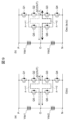
- FIG. 1 is a schematic diagram showing a power converter according to a reference example.
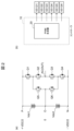
- FIG. 2 is a circuit diagram showing a U-phase circuit of FIG. 1 .
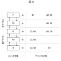
- FIG. 11 is a state transition diagram showing a control method for an ANPC inverter in a reference example.
- 4 is a time chart showing a control method for an ANPC inverter in a reference example.
- FIG. 13 is a diagram for explaining a case where switching loss and switching surge occur in a negative cycle.
- FIG. 11 is a diagram for comparing switching surge voltages and losses in a reference example.
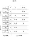
- FIG. 4 is a state transition diagram showing a control method for an ANPC inverter in the first embodiment of the present invention.
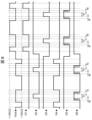
- FIG. 4 is a time chart showing a control method for an ANPC inverter in the first embodiment of the present invention.
- 4A and 4B are diagrams for explaining currents flowing in state O and state Oec;
- FIG. 4 is a diagram for comparing switching surge voltages and losses in the first embodiment of the present invention.
- 5 is a time chart for explaining a difference in switching delay time in the first embodiment.
- FIG. 1 is a schematic diagram showing a three-phase inverter power converter, which is also described in Patent Document 1.
- the device in FIG. 1 is a three-level ANPC (Active Neutral-Point-Clamped) inverter (hereinafter simply referred to as an ANPC inverter) having three phases.
- ANPC inverter In the ANPC inverter, DC power sources Vdc1 and Vdc2 are connected in series.
- the high potential terminal of the DC power source Vdc1 is the P terminal
- the connection point between the DC power sources Vdc1 and Vdc2 is the O terminal which is a medium potential terminal
- the low potential terminal of the DC power source Vdc2 is the N terminal.
- a smoothing capacitor C1 is connected between the P terminal and the O terminal
- a smoothing capacitor C2 is also connected between the O terminal and the N terminal.
- a plurality of capacitors C1 and C2 may be connected in parallel.
- the P, O, and N terminals are further connected to main circuit parts which are the U, V, and W phases.
- the U-phase includes a first switching element Q1, a second switching element Q2, a third switching element Q3, a fourth switching element Q4, a fifth switching element Q5, and a sixth switching element Q6.
- Each switching element is a MOSFET, but is not limited to this, and may be a parallel connection of a semiconductor switching element and a diode.
- the semiconductor switching element may be, for example, a semiconductor switching element such as an IGBT other than a MOSFET.
- the diode may be, for example, a PN junction diode, a Schottky barrier diode, or other diode.
- the materials of the above switching elements may be Si, SiC, GaN, GaO, or other materials. Two or more types of the above switching elements may be hybrid-implemented. In FIG. 2(a), the capacitor is omitted. In the following, to avoid redundant expressions, "switching elements Q1 to Q6" may be simply referred to as "Q1 to Q6".
- the first switching element Q1, the second switching element Q2, the third switching element Q3, and the fourth switching element Q4 are connected in series in this order between terminal P and terminal N.
- the fifth switching element Q5 is connected between the intermediate connection point between the first switching element Q1 and the second switching element Q2 and the O terminal.
- the sixth switching element Q6 is connected between the intermediate connection point between the third switching element Q3 and the fourth switching element Q4 and the O terminal.
- the intermediate connection point between the second switching element Q2 and the third switching element Q3 is called the AC terminal, and the AC terminal is connected to the load (see Figure 1).
- the switching of the switching elements Q1 to Q6 is controlled by individual gate drivers (GD).
- the switching signals of the individual gate drivers are generated by the PWM generator 20 of the controller 10.
- DC power sources Vdc1 and Vdc2 have a voltage of half the bus voltage, in other words, VDC/2.
- the O terminal is considered to be a voltage neutral point with a potential of 0.
- the potential of the P terminal is +VDC/2
- the potential of the N terminal is -VDC/2.
- the voltage between the P terminal and the N terminal is exactly the bus voltage VDC.
- FIG. 3 is a state transition diagram showing the control method of the ANPC inverter in the reference example, showing the switch states and the switching elements that are ON corresponding to the switch states.
- Figure 4 is a time chart showing the control method in the reference example, showing the ON/OFF of each switching element and the voltage Vout of the AC terminal.
- Figure 5 is a diagram for explaining a case in which switching loss and switching surge occur in the negative cycle.
- state P, state O, and state N the states when the AC terminals are energized with the P terminal, O terminal, and N terminal are called state P, state O, and state N, respectively.
- State P, state O, and state N correspond to tp, to, and tn, respectively, shown in Figure 4.
- the transition between state P and state O is called a positive cycle
- the transition between state O and state P is called a negative cycle.
- the operation of the positive cycle is the same as the negative cycle, so a description will be omitted and only the transition operation of the negative cycle will be described.
- switching elements Q3, Q4, and Q5 are ON, and the voltage at the AC terminal is -VDC/2.
- state O to
- switching elements Q2, Q3, Q5, and Q6 are ON, and the output voltage at the AC terminal is 0.
- current is flowing simultaneously through route 1 (Q2 and Q5) and route 2 (Q3 and Q6) between the O terminal and the AC terminal, and equal current flows through both paths.
- the intermediate state NO (tx) is passed through once (state PO (ty) in the case of a positive cycle).
- switching elements Q3 and Q5 are ON.
- switching element Q4 when shifting from state N to state NO, switching element Q4 turns off. If the conductive current in state N flows from the AC terminal to the N terminal, switching loss and surge voltage occur in switching element Q4 when it is turned off.
- switching elements Q2 and Q6 turn on simultaneously.
- a conducting current state O
- turn-on switching loss occurs in switching elements Q2 and Q6, and recovery loss and recovery surge occur in switching element Q4.
- FIG. 6 is a diagram comparing the surge voltages and losses that occur in switching elements Q2, Q3, Q5, and Q6 in the reference example.
- the surge voltage refers to an overvoltage that occurs when the parasitic capacitance of a switching element is excessively charged due to the influence of inductance components near the element when the switching element is turned off.
- the path on which the switching element Q6 is located is O terminal ⁇ Q6 ⁇ Q4 ⁇ N terminal.
- the path on which the switching element Q2 is located is O terminal ⁇ Q5 ⁇ Q2 ⁇ Q3 ⁇ Q4 ⁇ N terminal, which is longer than the path on which the switching element Q6 is located. Therefore, the surge voltage generated in the switching element Q2 is greater than the surge voltage generated in the switching element Q6.
- the surge voltage generated in the switching element Q3 is greater than the surge voltage generated in the switching element Q5.
- the switching surge voltages generated in the switching elements Q2 and Q3 are greater than the switching surge voltages generated in the switching elements Q5 and Q6.
- the losses that occur in switching elements include conduction losses caused by heat generated while current is flowing, and switching losses caused by heat generated during switching. The magnitude of these losses is proportional to the magnitude of the current flowing through the element.
- a conducting current flows through switching element Q4 in state N, and a conducting current flows through switching element Q6 in state O.
- a conducting current flows through switching element Q3 in both state O and state N. Therefore, it can be seen that the conducting loss of switching element Q3 is higher than the conducting losses of switching elements Q4 and Q6. Also, since the conducting current flows equally through switching elements Q3 and Q6 in state O, the currents flowing through switching elements Q3 and Q6 when switching are also equal. Therefore, the switching losses occurring in switching elements Q3 and Q6 are comparable. Therefore, when considering the total loss (conduction loss and switching loss), it can be seen that the loss occurring in switching element Q3 is greater than the loss occurring in switching element Q6.
- the loss occurring in switching element Q2 is greater than the loss occurring in switching element Q5.
- the losses occurring in switching elements Q2 and Q3 are greater than the losses occurring in switching elements Q5 and Q6.
- switching elements Q2 and Q3 are greater than switching elements Q5 and Q6 in terms of both loss and surge voltage. In this way, in an ANPC inverter, problems arise in terms of loss and surge voltage imbalance between switching elements.
- Fig. 7 is a state transition diagram showing a control method of the ANPC inverter in the embodiment 1 of the present invention.
- Fig. 8 is a time chart showing a control method of the ANPC inverter in the embodiment 1. Below, differences from the reference example will be described.
- the state transition diagram of the reference example differs in that a state Odf has been added between state PO and state O, and a state Oec has been added between state NO and state O.
- State Odf corresponds to td and tf shown in FIG. 7
- state Oec corresponds to te and tc shown in FIG. 7.
- times te and tc are added before and after a time to.
- times te and tc in the negative cycle are times when only switching elements Q3 and Q5 are ON, and no current flows anywhere. This time is defined as dead time in this specification. The same applies to tf and td in the positive cycle.
- the operation of the positive cycle is the same as the negative cycle, so the explanation is omitted and only the transition operation of the negative cycle will be explained.
- FIG. 9 there are two current conduction routes in state O and state Oec.
- state Oec switching element Q2 is turned OFF from state O and switching elements Q3, Q5 and Q6 are turned ON, and the current mainly flows through route 2.
- state Oec switching elements Q3, Q5 and Q6 are also ON
- state O Q2, Q3, Q5 and Q6 are ON
- the current first mainly flows through route 2 at the moment of transition to state Oec.
- switching element Q2 turns ON and transitions to state O, and the current is shared and flows evenly through both routes, route 1 and route 2.
- switching element Q6 is turned off and transition to state NO occurs.
- switching elements Q2 and Q6 are turned off simultaneously with current flowing evenly, and the same switching loss occurs, but in this embodiment, during the transition from state O to state NO, Q2 is first turned off with current flowing evenly through switching elements Q2 and Q6, and then Q6 is turned off with the current concentrated on route 2.
- the fifth switching element when transitioning between state O and state Oec, the fifth switching element at least performs one of the following operations: either completing turn-on before the third switching element or completing turn-off after the third switching element. Also, during a positive cycle, when transitioning between state O and state Odf, the sixth switching element at least performs one of the following operations: either completing turn-on before the second switching element or completing turn-off after the second switching element.
- the switching loss generated in Q6 is greater than the switching loss generated in Q2.
- the switching loss generated in Q5 is greater than the switching loss generated in Q3.
- the times te and tc in state Oec are shorter than the time to in state O. This is because by setting them in this way, the increase in the conduction loss of switching element Q6 in state Oec can be ignored.
- FIG. 10 is a diagram comparing the surge voltages and losses generated in switching elements Q2, Q3, Q5, and Q6 in this embodiment.
- the solid and dashed lines show the results of this embodiment and the reference example, respectively. Because switching element Q2 is switched with a smaller current than in the reference example, the surge voltage in switching element Q2 is reduced. On the other hand, because switching element Q6 is switched with a larger current than in the reference example, the surge voltage in switching element Q6 increases. The same is true for the positive cycle, where the surge voltage generated in switching element Q3 is reduced and the surge voltage generated in switching element Q5 increases. Therefore, the imbalance in the switching surge voltages in switching element Q2 (Q3) and switching element Q5 (Q6) is corrected and they become approximately the same.
- switching element Q2 was switched at a smaller current than in the reference example, the switching loss in switching element Q2 was reduced.
- switching element Q6 was switched at a larger current than in the reference example, so the switching loss in switching element Q6 increased.
- the conduction loss is negligible and is therefore about the same as in the reference example. Therefore, when considering the total loss (conduction loss and switching loss), the loss imbalance in switching element Q2 (Q3) and switching element Q5 (Q6) is corrected and is about the same.
- this embodiment reduces the loss and surge voltage imbalance in the switching elements of the ANPC inverter.
- state Oec Q3, Q5 and Q6 are ON
- state O Q2, Q3, Q5 and Q6 are ON
- Q6 is turned ON before Q2 when transitioning from state NO to state O
- Q6 is turned OFF after Q2 when transitioning from state O to state NO.
- ON and OFF respectively refer to “completion of turn-on operation” and “completion of turn-off operation", and more specifically, to “maximization of the main current flowing through the element” and “minimization of the main current flowing through the element”.
- start of turn-on (turn-off) refers to the start of the rise (fall) of the voltage applied to the element.
- completion of turn-on (turn-off) refers to the net drain current becoming 100% (0%), respectively.
- the settings of te, tc, td, and tf may be set by the PWM generator 20 on the controller 10 side as shown in FIG. 2, or may be set by adding a time adjustment circuit between the PWM generator 20 and the gate driver, or may be set by adding a time adjustment circuit inside the gate driver.
- the turn-on speed of the switching element Q5 (Q6) is set to be faster than that of the switching element Q2 (Q3).
- the turn-on drive resistance of the switching element Q5 (Q6) is set to be smaller than the turn-on drive resistance of the switching element Q2 (Q3).
- switching element Q5 an element having a lower threshold voltage than switching element Q2 (Q3) is selected as switching element Q5 (Q6). Then, even if the gate voltages of switching element Q5 (Q6) and switching element Q2 (Q3) start to rise at the same time, the gate voltage of switching element Q5 (Q6) exceeds the threshold voltage first, and the main current starts to flow through switching element Q5 (Q6) before switching element Q2 (Q3). On the other hand, even if the gate voltages of switching element Q5 (Q6) and switching element Q2 (Q3) start to drop at the same time, the threshold voltage of switching element Q5 (Q6) is low, so the timing at which the main current stops dropping is delayed.
- switching elements when turned on, current begins to flow through switching element Q5 (Q6) before switching element Q2 (Q3), resulting in a larger current when turned on and a larger turn-on loss. Also, when turned off, the main current takes a longer time to fall in switching element Q5 (Q6) than in switching element Q2 (Q3), resulting in a larger current when turned off, and larger turn-off losses and surge voltages. Therefore, as in the previously described embodiments, the imbalance in losses and surge voltages in the switching elements is corrected.
- Example 4 Next, a power converter according to a fourth embodiment will be described.
- the fourth embodiment will be described mainly with respect to differences from the above-described embodiments.
- a shift in switching timing is achieved by setting different gate voltages (negative bias) when the switching element Q6 (Q5) and the switching element Q2 (Q3) are turned off.
- the OFF gate voltage of switching element Q5 (Q6) is adjusted to be higher than the OFF gate voltage of switching element Q2 (Q3).
- the OFF gate voltage of switching element Q5 (Q6) is adjusted to -1V
- the OFF gate voltage of switching element Q2 (Q3) is adjusted to -3V. Then, even if the gate voltages of switching element Q5 (Q6) and switching element Q2 (Q3) start to rise at the same timing and the same speed, the gate voltage of switching element Q5 (Q6) exceeds the threshold voltage first, and the main current starts to flow through switching element Q5 (Q6) before switching element Q2 (Q3).
- the power converter of the present invention is a power converter having first and second capacitors connected in series between the positive and negative poles of a DC power source, first to fourth switching elements further connected in series in this order between the positive and negative poles of the DC power source and in parallel with the first and second capacitors, a fifth switching element connected between the connection point of the first and second switching elements and the connection point of the first and second capacitors, a sixth switching element connected between the connection point of the third and fourth switching elements and the connection point of the first and second capacitors, and a load connected to the connection point of the second and third switching elements, wherein a first output state is a state in which the first, second and sixth switching elements are ON and the third, fourth and fifth switching elements are OFF, a second output state is a state in which the third, fourth and fifth switching elements are ON and the first, second and sixth switching elements are OFF, and a load connected to the connection point of the second and third switching elements.
- the third output state is a state in which the third and fifth switching elements are ON and the first, second, fourth and sixth switching elements are OFF
- the first dead time state is a state in which the second and sixth switching elements are ON and the first, third, fourth and fifth switching elements are OFF
- the second dead time state is a state in which the second and sixth switching elements are ON and the first, third, fourth and fifth switching elements are OFF
- the third output state and the first output state are switched via the second dead time state
- the third output state and the second output state are switched via the first dead time state
- the fifth switching element performs at least one of the following operations: completing turn-on before or completing turn-off after the third switching element, or when transitioning between the third output state and the first dead time
- the sixth switching element performs at least one of the following operations: completing turn-on before or completing turn-off after the second switching element.
- the above configuration makes it possible to correct the imbalance in surge voltage and loss between switching elements, thereby improving power efficiency.
- the fifth switching element starts to turn off with a delay of at least the time from when the gate voltage of the third switching element starts to fall until the main current starts to fall, or when transitioning from the third output state to the first dead time, the sixth switching element starts to turn off with a delay of at least the time from when the gate voltage of the second switching element starts to fall until the main current starts to fall.
- the fifth switching element starts to turn on before the third switching element starts to turn on for at least the time from when the gate voltage of the fifth switching element starts to rise to when the main current starts to rise, or when transitioning from the first dead time to the third output state, the sixth switching element starts to turn on before the second switching element starts to turn on for at least the time from when the gate voltage of the sixth switching element starts to rise to when the main current starts to rise.
- the turn-on drive resistance of the fifth switching element is set lower than the turn-on drive resistance of the third switching element so that the turn-on speed of the fifth switching element is faster than the turn-on speed of the third switching element, or the turn-on drive resistance of the sixth switching element is set lower than the turn-on drive resistance of the second switching element so that the turn-on speed of the sixth switching element is faster than the turn-on speed of the second switching element.
- the turn-on gate current of the fifth switching element is set higher than the turn-on gate current of the third switching element so that the turn-on speed of the fifth switching element is faster than the turn-on speed of the third switching element, or the turn-on gate current of the sixth switching element is set higher than the turn-on gate current of the second switching element so that the turn-on speed of the sixth switching element is faster than the turn-on speed of the second switching element.
- the turn-off drive resistance of the fifth switching element is set higher than the turn-on drive resistance of the third switching element so that the turn-off speed of the fifth switching element is slower than the turn-off speed of the third switching element, or the turn-off drive resistance of the sixth switching element is set higher than the turn-off drive resistance of the second switching element so that the turn-off speed of the sixth switching element is slower than the turn-off speed of the second switching element.
- the turn-off gate current of the fifth switching element is set lower than the turn-on gate current of the third switching element so that the turn-off speed of the fifth switching element is slower than the turn-on speed of the third switching element, or the turn-off gate current of the sixth switching element is set lower than the turn-off gate current of the second switching element so that the turn-off speed of the sixth switching element is slower than the turn-off speed of the second switching element.
- the fifth switching element and the third switching element are selected so that the threshold voltage of the fifth switching element is lower than the threshold voltage of the third switching element, or the sixth switching element and the second switching element are selected so that the threshold voltage of the sixth switching element is lower than the threshold voltage of the second switching element.
- Vdc1-Vdc2 DC power supply
- C1-C2 smoothing capacitors (first and second capacitors)
- L load
- Q1-Q6 semiconductor switching elements (first to sixth switching elements)
Landscapes
- Engineering & Computer Science (AREA)
- Power Engineering (AREA)
- Inverter Devices (AREA)
Abstract
電力変換器は、第1と第2のキャパシタと、第1から第6のスイッチング素子と、負荷と、を有し、第3出力状態と第1出力状態との切り替えは第2デッドタイム状態を経由し、第3出力状態と第2出力状態との切り替えは第1デッドタイム状態を経由し、第3出力状態と第2デッドタイム状態との間で互いに遷移する際、第5のスイッチング素子は第3のスイッチング素子より先にターンオンを完了するかまたは遅れてターンオフを完了するかの少なくともいずれかの動作を実行し、または、第3出力状態と第1デッドタイム状態との間で互いに遷移する際、第6のスイッチング素子は第2のスイッチング素子より先にターンオンを完了するかまたは遅れてターンオフを完了するかの少なくともいずれかの動作を実行する。
Description
本発明は、3レベルインバータを含む電力変換器に関する。
近年、電力変換器の高バス電圧化のニーズに対して、マルチレベルインバータが活発的に検討されている。例えば、特許文献1にはANPC(Active Neutral-Point-Clamped)というマルチレベルインバータの回路が提案されている。
しかしながら、従来技術においては、スイッチング素子間におけるサージ電圧及び損失のアンバランスがあり、電力効率や信頼性の低下という課題があった。
本発明は、上記課題に鑑みてなされたものであり、その目的は、スイッチング素子間のサージ電圧及び損失のアンバランスを是正でき、電力効率を高めることができる電力変換器を提供することである。
本発明に係る電力変換器は、直流電源の正極と負極間に第1と第2のキャパシタを直列に接続し、直流電源の正極と負極間にさらに第1から第4のスイッチング素子を直列に接続し、第1と第2のスイッチング素子の接続点と第1と第2のキャパシタの接続点との間には第5のスイッチング素子を接続し、第3と第4のスイッチング素子の接続点と第1と第2のキャパシタの接続点との間には第6のスイッチング素子を接続し、第2と第3のスイッチング素子の接続点と負荷とを接続する電力変換器であって、第1、第2及び第6のスイッチング素子がONであり、第3、第4及び第5のスイッチング素子がOFFの状態を第1出力状態とし、第3、第4及び第5のスイッチング素子がONであり、第1、第2及び第6のスイッチング素子がOFFの状態を第2出力状態とし、第2、第3、第5及び第6のスイッチング素子がONであり、第1及び第4のスイッチング素子がOFFの状態を第3出力状態とし、第3及び第5のスイッチング素子がONであり、第1、第2、第4及び第6のスイッチング素子がOFFの状態を第1デッドタイム状態とし、第2及び第6のスイッチング素子がONであり、第1、第3、第4及び第5のスイッチング素子がOFFの状態を第2デッドタイム状態とし、第3出力状態と第1出力状態との切り替えは第2デッドタイム状態を経由し、第3出力状態と第2出力状態との切り替えは第1デッドタイム状態を経由し、第3出力状態と第2デッドタイム状態との間で互いに遷移する際、第5のスイッチング素子は第3のスイッチング素子より先にターンオンを完了するかまたは遅れてターンオフを完了するかの少なくともいずれかの動作を実行し、または、第3出力状態と第1デッドタイム状態との間で互いに遷移する際、第6のスイッチング素子は第2のスイッチング素子より先にターンオンを完了するかまたは遅れてターンオフを完了するかの少なくともいずれかの動作を実行する。
本開示によれば、スイッチング素子間のサージ電圧および損失のアンバランスを是正でき、電力効率を高めることができる電力変換器を提供することが可能になる。
本発明に関連する更なる特徴は、本明細書の記述、添付図面から明らかになるものである。また、上記した以外の課題、構成および効果は以下の実施形態の説明により明らかにされる。
本発明に関連する更なる特徴は、本明細書の記述、添付図面から明らかになるものである。また、上記した以外の課題、構成および効果は以下の実施形態の説明により明らかにされる。
まず以下では、本実施例を理解するに際して有用となる参考例について図面に沿って説明する。以下では、三相インバータ電力変換装置を例とするが、単相インバータ、多相インバータ、コンバータにも適用することが可能である。
図1は、特許文献1にも記載されている、三相インバータ電力変換器を示す概要図である。図1の装置は3相を持つ3level ANPC(Active Neutral-Point-Clamped)インバータ(以下では単にANPCインバータと呼称する)である。図1に示すように、ANPCインバータにおいては直流電源Vdc1とVdc2は直列に接続される。直流電源Vdc1の高電位端子はP端子、直流電源Vdc1とVdc2との接続点は中電位端子のО端子、直流電源Vdc2の低電位端子はN端子とする。P端子とО端子は平滑用のキャパシタC1が接続され、О端子とN端子との間にも平滑用のキャパシタC2が接続される。キャパシタC1およびC2は複数個並列接続されてもよい。P、O、N端子はさらにU、V、W相となる主回路部分が接続される。
図1は、特許文献1にも記載されている、三相インバータ電力変換器を示す概要図である。図1の装置は3相を持つ3level ANPC(Active Neutral-Point-Clamped)インバータ(以下では単にANPCインバータと呼称する)である。図1に示すように、ANPCインバータにおいては直流電源Vdc1とVdc2は直列に接続される。直流電源Vdc1の高電位端子はP端子、直流電源Vdc1とVdc2との接続点は中電位端子のО端子、直流電源Vdc2の低電位端子はN端子とする。P端子とО端子は平滑用のキャパシタC1が接続され、О端子とN端子との間にも平滑用のキャパシタC2が接続される。キャパシタC1およびC2は複数個並列接続されてもよい。P、O、N端子はさらにU、V、W相となる主回路部分が接続される。
U相を例として具体的構成を図2で説明する。図2(a)に示すように、U相は第1スイッチング素子Q1、第2スイッチング素子Q2、第3スイッチング素子Q3、第4スイッチング素子Q4、第5スイッチング素子Q5、および第6スイッチング素子Q6を備える。各スイッチング素子はMOSFETであるが、これに限ったものではなく、半導体スイッチング素子とダイオードの並列接続体であってもよい。また半導体スイッチング素子は例えば、MOSFET以外にもIGBTなどの半導体スイッチング素子であってよい。ダイオードは例えば、PN接合型ダイオード、ショットキーバリアダイオードなどのダイオードであってよい。以上のスイッチング素子の材料はSi、SiC、GaN、GaOなどの材料であってよい。また、以上のスイッチング素子を2種類以上ハイブリッド実装してもよい。図2(a)においてはキャパシタの図示は省略している。なお以下では冗長な表現を避けるために「スイッチング素子Q1~Q6」を単に「Q1~Q6」と呼称することがある。
第1スイッチング素子Q1、第2スイッチング素子Q2、第3スイッチング素子Q3、第4スイッチング素子Q4はこの順に、端子Pから端子Nまでの間に直列に接続されている。第1スイッチング素子Q1と第2スイッチング素子Q2との中間接続点とО端子との間に第5スイッチング素子Q5が接続されている。第3スイッチング素子Q3と第4スイッチング素子Q4との中間接続点とO端子との間に第6スイッチング素子Q6が接続されている。また第2スイッチング素子Q2と第3スイッチング素子Q3との中間接続点をAC端子と呼び、AC端子は負荷(図1参照)と接続されている。
また図2(b)に示すように、スイッチング素子Q1~Q6のスイッチングは個々のゲートドライバ(GD)が制御する。個々のゲートドライバのスイッチング信号はコントローラ10のPWM生成器20から生成される。
次に、ANPCインバータの通電方式について説明する。通常、直流電源Vdc1とVdc2はバス電圧の半分、つまりVDC/2の電圧を持つ。また、О端子を電位0の電圧中性点とする。そうすると、P端子の電位が+VDC/2となり、N端子の電位が-VDC/2となる。P端子とN端子の間はちょうどバス電圧VDCとなる。この状態でAC端子とP端子とを通電しようとするには、少なくとも第1スイッチング素子Q1および第2スイッチング素子Q2を同時にONする必要がある。同様に、AC端子とN端子とを通電しようとするには、少なくとも第3スイッチング素子Q3および第4スイッチング素子Q4を同時にONする必要がある。
一方、AC端子とО端子と通電する場合は二つの経路がある。すなわち後述する図9に示すように、第2スイッチング素子Q2と第5スイッチング素子Q5とを同時にONしてなる第1経路(ルート1)、および第3スイッチング素子Q3と第6スイッチング素子Q6とを同時にONしてなる第2経路(ルート2)がある。AC端子とО端子と通電しようとするには、この二つの経路の少なくとも一つを通電状態にする必要がある。AC端子がそれぞれP端子、О端子およびN端子と通電した場合はAC端子の電位がそれぞれ+VDC/2、0、-VDC/2電圧となる。このように、AC端子の電圧出力レベルは3段階になる。
次に、ANPCインバータの制御方式、特にAC端子とО端子とを前記の二つの経路によって通電する参考例の制御方式について図3~図5を参照して説明する。図3は参考例におけるANPCインバータの制御方式を表す状態転移図であり、スイッチの状態と、当該スイッチの状態に対応してONになっているスイッチング素子を示している。図4は参考例における制御方式を表すタイムチャートであり、各スイッチング素子のON/OFF及びAC端子の電圧Voutを示している。図5は負サイクルにおいてスイッチング損失とスイッチングサージが発生するケースを説明するための図である。
まず図3に示すように、AC端子がそれぞれP端子、О端子およびN端子と通電した時の状態をそれぞれ状態P、状態Oおよび状態Nという。状態P、状態Oおよび状態Nはそれぞれ図4に示すtp、toおよびtnに対応する。状態Pと状態Oとの間の転移を正サイクルといい、状態Oと状態Pと間の転移を負サイクルという。正サイクルの動作は負サイクルと同様のため説明を省略し、負サイクルの転移動作のみを説明する。
図3および図4に示すように、状態N(tn)のとき、スイッチング素子Q3、Q4及びQ5がONしていて、AC端子の電圧が-VDC/2である。状態O(to)のとき、スイッチング素子Q2、Q3、Q5およびQ6がONしていて、AC端子の出力電圧が0である。ここで、状態OのときはO端子とAC端子との間はルート1(Q2及びQ5)及びルート2(Q3及びQ6)が同時に通電している状態であり、両経路上は均等の電流が流れる。そして状態Nからと状態Oへと転移するときは一旦状態NO(tx)という中間状態を経由する(正サイクルの場合は状態PO(ty))。状態NO(tx)の時、スイッチング素子Q3およびQ5がONしている。
ここで、スイッチング素子がスイッチングされるとき、導通時における電流の方向がスイッチング素子の備えるダイオードの順方向と逆になる場合、該スイッチング素子にはスイッチング損失とサージ電圧が発生する。図5は損失とサージ電圧が発生するケースを示す図である。図5は、状態Nまたは状態Oと中間状態NOとの間で転移するケースを示しており、損失またはサージが発生するスイッチング素子は「〇」マークで囲んでいる。
まず図5(a)に示すように、状態NOから状態Nにシフトするとき、スイッチング素子Q4がターンオンする。ターンオン後(状態N)の電流がAC端子からN端子に流れ込む場合、スイッチング素子Q4にターンオンのスイッチング損失が生じ、スイッチング素子Q2とQ6にはリカバリの損失およびリカバリサージが生じる。
一方、図5(b)に示すように、状態Nから状態NOにシフトするとき、スイッチング素子Q4がターンオフする。状態Nでの導通電流がAC端子からN端子に流れていた場合、スイッチング素子Q4にターンオフのスイッチング損失およびサージ電圧が生じる。
次に、図5(c)に示すように、状態NOから状態Oにシフトするとき、スイッチング素子Q2およびQ6が同時にターンオンする。導通電流(状態O)がO端子からAC端子に流れる場合、スイッチング素子Q2およびQ6にターンオンのスイッチング損失が生じ、スイッチング素子Q4にはリカバリの損失およびリカバリサージが生じる。
そして、図5(d)に示すように、状態Oから状態NOにシフトするとき、スイッチング素子Q2およびQ6が同時にターンオフする。状態Oで電流がO端子からAC端子に流れていた場合、スイッチング素子Q2およびQ6にターンオフ損失およびサージ電圧が生じる。
図6は参考例においてスイッチング素子Q2、Q3、Q5およびQ6に生じるサージ電圧と損失とを比較した図である。まずはこれらに発生するサージ電圧の差について説明する。ここでサージ電圧とは、スイッチング素子のターンオフの際に、素子近傍のインダクタンス成分の影響で、スイッチング素子の寄生容量が過大に充電されることに起因する過電圧のことである。
通常、回路のインダクタンス成分が大きいほどスイッチング素子に生じるサージ電圧も高くなるが、スイッチング素子Q2とQ6が所在する経路(O端子から出発してN端子に戻る経路)上のインダクタンス成分が異なるため、両スイッチング素子に生じるサージ電圧に差が生じる。具体的には、スイッチング素子Q6が所在する経路はO端子→Q6→Q4→N端子である。一方スイッチング素子Q2が所在する経路はO端子→Q5→Q2→Q3→Q4→N端子であり、前記Q6が所在する経路より長いことがわかる。よって、スイッチング素子Q2に発生するサージ電圧のほうがスイッチング素子Q6に発生するサージ電圧より大きくなる。正サイクルにおいても同様であり、スイッチング素子Q3に発生するサージ電圧のほうがスイッチング素子Q5に発生するサージ電圧より大きくなる。まとめると、図6(a)に示すように、スイッチング素子Q2及びQ3に発生するスイッチングサージ電圧は、スイッチング素子Q5及びQ6に発生するスイッチングサージ電圧より大きい。
次に上記のスイッチング素子に生じる損失の差について説明する。ここで、スイッチング素子に発生する損失には、電流が流れている間に生じる熱に起因する導通損失と、スイッチングの際に発生する熱に起因するスイッチング損失がある。これらの損失の大きさは、素子に流れる電流の大きさに比例する。
スイッチング素子Q4には状態Nの時に導通電流が流れ、スイッチング素子Q6には状態Oの時に導通電流が流れる。これらに対して、スイッチング素子Q3には状態Oの時も状態Nの時も導通電流が流れる。そのため、スイッチング素子Q3の導通損失はスイッチング素子Q4とQ6の導通損失より高いことがわかる。また、状態Oで導通電流がスイッチング素子Q3およびQ6に均等に流れるため、スイッチング素子Q3およびQ6がスイッチングする時の電流も均等である。よって、スイッチング素子Q3およびQ6に発生するスイッチング損失は同程度である。したがって、合計損失(導通損失とスイッチング損失)を考えると、スイッチング素子Q3に発生する損失はスイッチング素子Q6に発生する損失より大きいことがわかる。正サイクルにおいても同様であり、合計損失を考えると、スイッチング素子Q2に発生する損失はスイッチング素子Q5に発生する損失より大きい。まとめると、図6(b)に示すように、スイッチング素子Q2及びQ3に発生する損失は、スイッチング素子Q5及びQ6に発生する損失より大きい。
以上のように、図6に示すように、スイッチング素子Q2及びQ3においては損失とサージ電圧の両面でスイッチング素子Q5およびQ6より大きいことがわかる。このように、ANPCインバータにおいては、スイッチング素子間において損失及びサージ電圧のアンバランスという課題が発生する。
<実施例1>
以下、図面を参照しながら本発明の実施例を説明する。図7は本発明の実施例1におけるANPCインバータの制御方式を表す状態転移図である。図8は実施例1におけるANPCインバータの制御方式を表すタイムチャートである。以下では参考例との差分について説明する。
以下、図面を参照しながら本発明の実施例を説明する。図7は本発明の実施例1におけるANPCインバータの制御方式を表す状態転移図である。図8は実施例1におけるANPCインバータの制御方式を表すタイムチャートである。以下では参考例との差分について説明する。
本実施例においては、参考例の状態転移図より、状態POと状態Oの間に状態Odfを追加し、状態NOと状態Oの間に状態Oecを追加した点が異なる。状態Odfは図7に示すtdおよびtfに対応し、状態Oecは図7に示すteおよびtcに対応する。図8に示す本実施例におけるタイムチャートは図4に示す参考例のタイムチャートと比較して、toという時間の前後にteとtc(正サイクルにおいてはtfとtd)という時間が追加されることがわかる。これらの時間においては例えば負サイクルにおける時間teとtcはスイッチング素子Q3とQ5のみがONになっている時間であり、電流はどこにも流れない。この時間のことを本明細書においてはデッドタイムと定義する。正サイクルにおけるtfとtdについても同様である。
本実施例においても、正サイクルの動作は負サイクルと同様のため説明を省略し、負サイクルの転移動作のみを説明する。図9に示すように、状態Oと状態Oecにおける電流導通ルートは二つある。状態Oecにおいては状態Oからスイッチング素子Q2がOFFしてスイッチング素子Q3、Q5およびQ6がONしている状態であり、電流が主にルート2に流れる。そうすると、状態NO(Q3及びQ5のみONの状態)から状態Oec(Q3及びQ5に加えてQ6もONの状態)を経由して状態O(Q2、Q3、Q5、及びQ6がONの状態)に転移するときを考えると、状態Oecに転移した瞬間に電流がまず主にルート2上に流れる。しばらくすると、スイッチング素子Q2がターンオンして状態Oに移行し、電流が分担され、ルート1とルート2の両経路上に均等に流れるようになる。
反対に、状態Oから状態Oecを経由して状態NOに転移するとき、電流がまず状態Oの両ルート上に均等に流れ、次に、状態Oecでルート1の電流が低減され、ルート2上の電流が増加していく。最終的にはルート1上に流れていた電流が全部ルート2に流れてもよい。この状態でスイッチング素子Q6がOFFされて状態NOへと移行する。つまり、参考例においては、状態Oから状態NOへと移行する間に、スイッチング素子Q2及びQ6は均等に電流が流れている状態で同時にOFFされ、同等のスイッチング損失が発生していたが、本実施例においては、状態Oから状態NOへと移行する間に、まずスイッチング素子Q2及びQ6に均等に電流が流れている状態でQ2がOFFされ、その後ルート2上に電流が集約された状態でQ6がOFFされている。
これらをまとめると、状態Oと状態Oecとの間で互いに遷移する際、第5のスイッチング素子は第3のスイッチング素子より先にターンオンを完了するかまたは遅れてターンオフを完了するかの少なくともいずれかの動作を実行する、ということになる。また正サイクルのときも、状態Oと状態Odfとの間で互いに遷移する際、第6のスイッチング素子は第2のスイッチング素子より先にターンオンを完了するかまたは遅れてターンオフを完了するかの少なくともいずれかの動作を実行する、ということになる。
上述のように、参考例においてはスイッチング素子Q2及びQ6に流れるスイッチング時の電流は均等であったが、本実施例の場合、スイッチング素子Q6はスイッチング素子Q2より大きい電流でスイッチングする。したがって、本実施例においては、Q6に発生するスイッチング損失は、Q2に発生するスイッチング損失よりも大きくなる。正サイクルにおいても同様であり、Q5に発生するスイッチング損失はQ3に発生するスイッチング損失よりも大きくなる。なお、Q2及びQ3のスイッチング損失については、それぞれターンオフした瞬間には参考例と異なりまだQ5及びQ6はONの状態であり、電流は完全に遮断されずにQ5及びQ6の方へと流れていく。従って、Q2及びQ3に発生するスイッチング損失は参考例の場合よりも小さくなる。
また、状態Oecの時間teおよびtcは状態Oの時間toより小さいことが好ましい。そのように設定することで、状態Oecにおけるスイッチング素子Q6の導通損失の増加を無視することができるようになるからである。
図10は本実施例においてスイッチング素子Q2、Q3、Q5及びQ6に発生するサージ電圧と損失を比較した図である。実線および破線がそれぞれ本実施例および参考例の結果である。スイッチング素子Q2は参考例より小さい電流でスイッチングされたため、スイッチング素子Q2におけるサージ電圧が低減される。一方、スイッチング素子Q6は参考例より大きい電流でスイッチングされたため、スイッチング素子Q6におけるサージ電圧が増加した。正サイクルについても同様であり、スイッチング素子Q3に発生するサージ電圧が低減し、スイッチング素子Q5に発生するサージ電圧のほうが増加する。したがって、スイッチング素子Q2(Q3)とスイッチング素子Q5(Q6)におけるスイッチングサージ電圧のアンバランスが是正され、同程度になる。
さらに、スイッチング素子Q2は参考例より小さい電流でスイッチングされたため、スイッチング素子Q2におけるスイッチング損失が低減される。一方、スイッチング素子Q6は参考例より大きい電流でスイッチングされたため、スイッチング素子Q6におけるスイッチング損失が増加した。導通損失は上述のように無視できるため参考例と同程度である。したがって、合計損失(導通損失とスイッチング損失)を考えると、スイッチング素子Q2(Q3)とスイッチング素子Q5(Q6)における損失アンバランスが是正され、同程度になる。
以上、本実施例によれば、ANPCインバータのスイッチング素子における損失およびサージ電圧のアンバランスが低減される。
上述した本実施例における効果を得るには、状態NO(Q3及びQ5がON)及び状態O(Q2、Q3、Q5及びQ6がON)間の移行時に状態Oec(Q3、Q5及びQ6がON)を経ることが必須である。すなわち、状態NOから状態Oに移行するまでにはQ6がQ2より先にONされ、状態Oから状態NOに移行するにはQ6がQ2より後にOFFされるか、のいずれかの動作を実行することが必須である。
ここで、本明細書における「ON」「OFF」とは、それぞれ「ターンオン動作の完了」及び「ターンオフ動作の完了」を指し、より具体的にはそれぞれ「素子に流れる主電流の最大化」及び「素子に流れる主電流の最小化」を指す。また、ターンオン(ターンオフ)の開始とは、素子に印加する電圧の上昇(下降)の開始を指す。また、ターンオン(ターンオフ)の完了とは、それぞれ正味のドレイン電流が100%(0%)になることを指す。
なお、以上の実施例1においては状態Oの前後にteとtc(tdとtf)の両方が設定されるが、状況によって、teまたはtc(tdまたはtf)の片方だけ設定してもよい。例えば、ターンオフ損失が顕著でアンバランスが大きい場合、tc(td)のみ設定してよい。さらに、te、tc、tdおよびtfの長さはスイッチング素子のスイッチング遅延時間(ゲート電圧の上昇あるいは降下から素子主電流の上昇あるいは降下までの時間)より長く設定したほうが好ましい。
上記の理由について図11を用いて説明する。スイッチング素子Q6(Q5)がターンオン開始(ゲート電圧上昇開始)してから実際にQ6(Q5)に電流が流れ始めるまで時間T1だけ要する。この時間T1の間にスイッチング素子Q2(Q3)のターンオンを開始してしまうと、Q6(Q5)に流れる電流が完全に上昇する前にQ2(Q3)にも電流が流れ始めてしまい、十分なアンバランス是正効果が得られないからである。
ターンオフ時も同様で、スイッチング素子Q2(Q3)がターンオフ開始してから実際にQ2(Q3)に流れる電流が減少し始めるまで時間T2だけ要する。この時間T2の間にスイッチング素子Q6(Q5)のターンオフを開始してしまうとQ2(Q3)に流れる電流が最小化する前にQ6(Q5)に流れる電流も下降し始めてしまい、十分なアンバランス是正効果が得られないからである。
te、tc、tdおよびtfの設定は図2に示す、コントローラ10側のPWM生成器20で設定してもよく、PWM生成器20からゲートドライバまでの間に時間調整回路を追加して設定してもよく、ゲートドライバ内部で時間調整回路を追加して設定してもよい。
<実施例2>
次に、実施例2に係る電力変換器について説明する。以下では実施例1と異なる部分について主に説明する。実施例1においては、te、tc、tdおよびtfというデッドタイムを設定して、スイッチング素子Q6(Q5)とスイッチング素子Q2(Q3)との間にスイッチングタイミングのずれを入れることによってサージ電圧及び損失のアンバランスを是正していた。これに対して本実施例においては、スイッチング素子Q6(Q5)とスイッチング素子Q2(Q3)に異なるスイッチングスピードを設定することでスイッチングタイミングのずれを実現する。
次に、実施例2に係る電力変換器について説明する。以下では実施例1と異なる部分について主に説明する。実施例1においては、te、tc、tdおよびtfというデッドタイムを設定して、スイッチング素子Q6(Q5)とスイッチング素子Q2(Q3)との間にスイッチングタイミングのずれを入れることによってサージ電圧及び損失のアンバランスを是正していた。これに対して本実施例においては、スイッチング素子Q6(Q5)とスイッチング素子Q2(Q3)に異なるスイッチングスピードを設定することでスイッチングタイミングのずれを実現する。
具体的には、スイッチング素子Q5(Q6)のターンオンスピードをスイッチング素子Q2(Q3)より速くなるように設定する。例えば、スイッチング素子Q5(Q6)のターンオン駆動抵抗をスイッチング素子Q2(Q3)のターンオン駆動抵抗より小さく設定する。
また、駆動抵抗以外に、駆動時の電流に設定してもよい。例えば、スイッチング素子Q5(Q6)のターンオンゲート電流をスイッチング素子Q2(Q3)のターンオンゲート電流より高く設定する。そうすると、スイッチング素子Q5(Q6)とスイッチング素子Q2(Q3)が同じタイミングでゲート電圧を上昇し始めても、スイッチング素子Q5(Q6)のゲート電圧が先に閾値電圧を超え、スイッチング素子Q5(Q6)にスイッチング素子Q2(Q3)より先に主電流が流れ始める。
一方、スイッチング素子Q5(Q6)のターンオフスピードをスイッチング素子Q2(Q3)より遅く設定することも可能である。例えば、スイッチング素子Q5(Q6)のターンオフ駆動抵抗をスイッチング素子Q2(Q3)のターンオフ駆動抵抗より大きく設定する。駆動抵抗以外に、駆動時の電流を設定してもよい。例えば、スイッチング素子Q5(Q6)のターンオフゲート電流をスイッチング素子Q2(Q3)のターンオンゲート抵抗より低く設定する。そうすると、スイッチング素子Q5(Q6)とスイッチング素子Q2(Q3)が同じタイミングでゲート電圧を降下し始めても、スイッチング素子Q5(Q6)のゲート電圧降下が遅くなるため、Q5(Q6)の主電流が降下し始めるタイミングもQ2(Q3)よりも遅れる。
各スイッチング素子のターンオン(ターンオフ)駆動抵抗またはターンオン(ターンオフ)ゲート電流を上記のように設定すると、各スイッチング素子を同時にターンオン開始させたとしても、スイッチング素子Q5(Q6)がスイッチング素子Q2(Q3)より先に電流が流れ始めるため、ターンオン時の電流が大きく、ターンオン損失がより大きくなる。また、同様に各スイッチング素子を同時にターンオフさせたとしてもターンオフ時にスイッチング素子Q5(Q6)がスイッチング素子Q2(Q3)より遅れて主電流が降下し始めるため、ターンオフ時の電流が大きく、ターンオフ損失およびサージ電圧がより大きくなる。したがって、実施例1と同様に、スイッチング素子における損失およびサージ電圧のアンバランスが是正される。
<実施例3>
次に、実施例3に係る電力変換器について説明する。以下では、実施例3のうち、既述の実施例と異なる部分について主に説明する。本実施例においては、スイッチング素子Q6(Q5)とスイッチング素子Q2(Q3)にそれぞれ異なる閾値電圧をもつ素子を選定することでスイッチングタイミングのずれを実現する。
次に、実施例3に係る電力変換器について説明する。以下では、実施例3のうち、既述の実施例と異なる部分について主に説明する。本実施例においては、スイッチング素子Q6(Q5)とスイッチング素子Q2(Q3)にそれぞれ異なる閾値電圧をもつ素子を選定することでスイッチングタイミングのずれを実現する。
具体的には、スイッチング素子Q5(Q6)としてスイッチング素子Q2(Q3)より小さい閾値電圧を有する素子を選定する。すると、スイッチング素子Q5(Q6)とスイッチング素子Q2(Q3)が同じタイミングでゲート電圧を上昇し始めても、スイッチング素子Q5(Q6)のゲート電圧が先に閾値電圧を超えて、スイッチング素子Q5(Q6)にスイッチング素子Q2(Q3)より先に主電流が流れ始める。一方、スイッチング素子Q5(Q6)とスイッチング素子Q2(Q3)が同じタイミングでゲート電圧を降下し始めても、スイッチング素子Q5(Q6)の閾値電圧が低いため、主電流降下終了タイミングが遅れる。
このようにスイッチング素子を選定すると、ターンオン時にスイッチング素子Q5(Q6)にスイッチング素子Q2(Q3)より先に電流が流れ始めるため、ターンオン時の電流が大きくなり、ターンオン損失もより大きくなる。また、ターンオフ時にスイッチング素子Q5(Q6)の方がスイッチング素子Q2(Q3)より主電流の降下時間が長いため、ターンオフ時の電流が大きくなり、ターンオフ損失およびサージ電圧もより大きくなる。したがって、既述の実施例と同様に、スイッチング素子における損失およびサージ電圧のアンバランスが是正される。
<実施例4>
次に、実施例4に係る電力変換器について説明する。実施例4のうち、既述の実施例と異なる部分について主に説明する。本実施例においては、スイッチング素子Q6(Q5)とスイッチング素子Q2(Q3)に異なるOFF時のゲート電圧(負バイアス)を設定することでスイッチングタイミングのずれを実現する。
次に、実施例4に係る電力変換器について説明する。実施例4のうち、既述の実施例と異なる部分について主に説明する。本実施例においては、スイッチング素子Q6(Q5)とスイッチング素子Q2(Q3)に異なるOFF時のゲート電圧(負バイアス)を設定することでスイッチングタイミングのずれを実現する。
具体的には、スイッチング素子Q5(Q6)のOFF時ゲート電圧をスイッチング素子Q2(Q3)のOFF時ゲート電圧より高くなるように調整する。例えば、スイッチング素子Q5(Q6)のOFF時ゲート電圧を-1Vに調整して、スイッチング素子Q2(Q3)のOFF時ゲート電圧を-3Vに調整する。すると、スイッチング素子Q5(Q6)とスイッチング素子Q2(Q3)が同じタイミングと同じスピードでゲート電圧を上昇し始めても、スイッチング素子Q5(Q6)のゲート電圧が先に閾値電圧を超えて、スイッチング素子Q5(Q6)にスイッチング素子Q2(Q3)より先に主電流が流れ始める。一方、ターンオフ時は、OFF時ゲート電圧が低いほどゲート電圧の降下も速く、つまりターンオフスピードも速い。そのため、スイッチング素子Q5(Q6)とスイッチング素子Q2(Q3)が同じタイミングでゲート電圧を降下し始めても、スイッチング素子Q5(Q6)のゲート電圧降下スピードが遅いため、電流降下し始めるタイミングも遅れる。
このように、ターンオン時にスイッチング素子Q5(Q6)がスイッチング素子Q2(Q3)より先に電流が流れ始めるため、ターンオン時の電流が大きく、ターンオン損失がより大きくなる。また、ターンオフ時にスイッチング素子Q5(Q6)がスイッチング素子Q2(Q3)より遅れて主電流が降下し始めるため、ターンオフ時の電流が大きくなり、ターンオフ損失およびサージ電圧もより大きくなる。したがって、既述の実施例と同様に、スイッチング素子における損失およびサージ電圧のアンバランスが是正される。
以上で説明した本発明の実施例により、以下の作用効果が得られる。
(1)本発明に係る電力変換器は、直流電源の正極と負極間に直列接続された第1と第2のキャパシタと、直流電源の正極と負極間にさらにこの順に直列接続され、かつ第1と第2のキャパシタと並列である第1から第4のスイッチング素子と、第1と第2のスイッチング素子の接続点と第1と第2のキャパシタの接続点との間に接続された第5のスイッチング素子と、第3と第4のスイッチング素子の接続点と第1と第2のキャパシタの接続点との間に接続された第6のスイッチング素子と、第2と第3のスイッチング素子の接続点に接続された負荷と、を有する電力変換器であって、第1、第2及び第6のスイッチング素子がONであり、第3、第4及び第5のスイッチング素子がオフの状態を第1出力状態とし、第3、第4及び第5のスイッチング素子がONであり、第1、第2及び第6のスイッチング素子がオフの状態を第2出力状態とし、第2、第3、第5及び第6のスイッチング素子がONであり、第1及び第4のスイッチング素子がオフの状態を第3出力状態とし、第3及び第5のスイッチング素子がONであり、第1、第2、第4及び第6のスイッチング素子がオフの状態を第1デッドタイム状態とし、第2及び第6のスイッチング素子がONであり、第1、第3、第4及び第5のスイッチング素子がオフの状態を第2デッドタイム状態とし、第3出力状態と第1出力状態との切り替えは第2デッドタイム状態を経由し、第3出力状態と第2出力状態との切り替えは第1デッドタイム状態を経由し、第3出力状態と第2デッドタイムとの間で互いに遷移する際、第5のスイッチング素子は第3のスイッチング素子より先にターンオンを完了するかまたは遅れてターンオフを完了するかの少なくともいずれかの動作を実行し、または、第3出力状態と第1デッドタイムとの間で互いに遷移する際、第6のスイッチング素子は第2のスイッチング素子より先にターンオンを完了するかまたは遅れてターンオフを完了するかの少なくともいずれかの動作を実行する。
上記構成により、スイッチング素子間のサージ電圧および損失のアンバランスを是正でき、電力効率を高めることが可能となる。
(2)第3出力状態から第2デッドタイムに遷移する際、第5のスイッチング素子は、第3のスイッチング素子のゲート電圧が下降し始めてから主電流が下降し始めるまでの時間分以上遅れてターンオフを開始する、または、第3出力状態から第1デッドタイムに遷移する際、第6のスイッチング素子は、第2のスイッチング素子のゲート電圧が下降し始めてから主電流が下降し始めるまでの時間分以上遅れてターンオフを開始する。これにより、第3(第2)のスイッチング素子の主電流が確実に下降し始めてから第5(第6)のスイッチング素子の主電流も下降することになるので、第5(第6)のスイッチング素子が先にターンオフ完了してしまうことを防止でき、確実にアンバランスを是正することが可能になる。
(3)第2デッドタイムから第3出力状態に遷移する際、第5のスイッチング素子は、該第5のスイッチング素子のゲート電圧が上昇し始めてから主電流が上昇し始めるまでの時間分以上、第3のスイッチング素子のターンオン開始より先にターンオンを開始する、または、第1デッドタイムから第3出力状態に遷移する際、第6のスイッチング素子は、該第6のスイッチング素子のゲート電圧が上昇し始めてから主電流が上昇し始めるまでの時間分以上、第2のスイッチング素子のターンオン開始より先にターンオンを開始する。これにより、(2)と同様に、第3(第2)のスイッチング素子が先にターンオン完了してしまうことを防止でき、確実にアンバランスを是正することが可能になる。
(4)第5のスイッチング素子のターンオンスピードが第3のスイッチング素子のターンオンスピードより速くなるよう、第5のスイッチング素子のターンオン駆動抵抗を第3のスイッチング素子のターンオン駆動抵抗より低く設定する、または、第6のスイッチング素子のターンオンスピードが第2のスイッチング素子のターンオンスピードより速くなるよう、第6のスイッチング素子のターンオン駆動抵抗を第2のスイッチング素子のターンオン駆動抵抗より低く設定する。これにより、第5(第6)のスイッチング素子と第3(第2)のスイッチング素子とを同時にターンオン開始したとしても、第5(第6)のスイッチング素子が先にターンオン完了するため、本発明の効果を確実に得られる。
(5)第5のスイッチング素子のターンオンスピードが第3のスイッチング素子のターンオンスピードより速くなるよう、第5のスイッチング素子のターンオンゲート電流を第3のスイッチング素子のターンオンゲート電流より高く設定する、または、第6のスイッチング素子のターンオンスピードが第2のスイッチング素子のターンオンスピードより速くなるよう、第6のスイッチング素子のターンオンゲート電流を第2のスイッチング素子のターンオンゲート電流より高く設定する。これにより、(4)と同様に、第5(第6)のスイッチング素子と第3(第2)のスイッチング素子とを同時にターンオン開始したとしても、第5(第6)のスイッチング素子が先にターンオン完了するため、本発明の効果を確実に得られる。
(6)第5のスイッチング素子のターンオフスピードが第3のスイッチング素子のターンオフスピードより遅くなるよう、第5のスイッチング素子のターンオフ駆動抵抗を第3のスイッチング素子のターンオン駆動抵抗より高く設定する、または、第6のスイッチング素子のターンオフスピードが第2のスイッチング素子のターンオフスピードより遅くなるよう、第6のスイッチング素子のターンオフ駆動抵抗を第2のスイッチング素子のターンオフ駆動抵抗より高く設定する。これにより、第5(第6)のスイッチング素子と第3(第2)のスイッチング素子とを同時にターンオフ開始したとしても、第5(第6)のスイッチング素子が後にターンオフ完了するため、本発明の効果を確実に得られる。
(7)第5のスイッチング素子のターンオフスピードが第3のスイッチング素子のターンオンスピードより遅くなるよう、第5のスイッチング素子のターンオフゲート電流を第3のスイッチング素子のターンオンゲート電流より低く設定する、または、第6のスイッチング素子のターンオフスピードが第2のスイッチング素子のターンオフスピードより遅くなるよう、第6のスイッチング素子のターンオフゲート電流を第2のスイッチング素子のターンオフゲート電流より低く設定する。これにより、(6)と同様に、第5(第6)のスイッチング素子と第3(第2)のスイッチング素子とを同時にターンオフ開始したとしても、第5(第6)のスイッチング素子が後にターンオフ完了するため、本発明の効果を確実に得られる。
(8)第5のスイッチング素子の閾値電圧が第3のスイッチング素子の閾値電圧より低くなるよう、第5のスイッチング素子と第3のスイッチング素子を選定する、または、第6のスイッチング素子の閾値電圧が第2のスイッチング素子の閾値電圧より低くなるよう、第6のスイッチング素子と第2のスイッチング素子を選定する。これにより、上記と同様、第5(第6)のスイッチング素子の方が第3(第2)スイッチング素子よりも先にターンオン(後にターンオフ)するので、本発明の効果を確実に得られる。
(9)第5のスイッチング素子のOFF時ゲート電圧が第3のスイッチング素子のOFF時ゲート電圧より高くなるよう、第5のスイッチング素子と第3のスイッチング素子のOFF時ゲート電圧を調整する、または、第6のスイッチング素子のOFF時ゲート電圧が第2のスイッチング素子のOFF時ゲート電圧より高くなるよう、第6のスイッチング素子と第2のスイッチング素子のOFF時ゲート電圧を調整する。これにより、(8)と同様の効果を得られる。
以上、本発明のいくつかの実施形態を説明したが、上述の実施形態に限られるものではなく、その趣旨を逸脱しない範囲において様々の構成で実現することができる。例えば、第1~4実施形態の設定方法を任意に組み合わせた構成も容易に考えられる。これらの変形は、特許請求の範囲に記載される発明とその均等の範囲に含まれる。
Vdc1~Vdc2・・・直流電源、C1~C2・・・平滑用コンデンサ(第1と第2のキャパシタ)、L・・・負荷、Q1~Q6・・・半導体スイッチング素子(第1から第6のスイッチング素子)
Claims (9)
- 直流電源の正極と負極間に第1と第2のキャパシタを直列に接続し、前記直流電源の正極と負極間にさらに第1から第4のスイッチング素子を直列に接続し、前記第1と第2のスイッチング素子の接続点と前記第1と第2のキャパシタの接続点との間には第5のスイッチング素子を接続し、前記第3と第4のスイッチング素子の接続点と前記第1と第2のキャパシタの接続点との間には第6のスイッチング素子を接続し、前記第2と第3のスイッチング素子の接続点と負荷とを接続する電力変換器であって、
前記第1、第2及び第6のスイッチング素子がONであり、前記第3、第4及び第5のスイッチング素子がOFFの状態を第1出力状態とし、前記第3、第4及び第5のスイッチング素子がONであり、前記第1、第2及び第6のスイッチング素子がOFFの状態を第2出力状態とし、前記第2、第3、第5及び第6のスイッチング素子がONであり、前記第1及び第4のスイッチング素子がOFFの状態を第3出力状態とし、
前記第3及び第5のスイッチング素子がONであり、前記第1、第2、第4及び第6のスイッチング素子がOFFの状態を第1デッドタイム状態とし、前記第2及び第6のスイッチング素子がONであり、前記第1、第3、第4及び第5のスイッチング素子がOFFの状態を第2デッドタイム状態とし、
前記第3出力状態と第1出力状態との切り替えは前記第2デッドタイム状態を経由し、前記第3出力状態と第2出力状態との切り替えは前記第1デッドタイム状態を経由し、
前記第3出力状態と前記第2デッドタイム状態との間で互いに遷移する際、前記第5のスイッチング素子は前記第3のスイッチング素子より先にターンオンを完了するかまたは遅れてターンオフを完了するかの少なくともいずれかの動作を実行し、または、前記第3出力状態と前記第1デッドタイム状態との間で互いに遷移する際、前記第6のスイッチング素子は前記第2のスイッチング素子より先にターンオンを完了するかまたは遅れてターンオフを完了するかの少なくともいずれかの動作を実行する、
ことを特徴とする電力変換器。 - 請求項1に記載の電力変換器であって、
前記第3出力状態から前記第2デッドタイム状態に遷移する際、前記第5のスイッチング素子は、前記第3のスイッチング素子のゲート電圧が下降し始めてから主電流が下降し始めるまでの時間分以上遅れてターンオフを開始する、または、
前記第3出力状態から前記第1デッドタイム状態に遷移する際、前記第6のスイッチング素子は、前記第2のスイッチング素子のゲート電圧が下降し始めてから主電流が下降し始めるまでの時間分以上遅れてターンオフを開始する、
ことを特徴とする電力変換器。 - 請求項1に記載の電力変換器であって、
前記第2デッドタイム状態から前記第3出力状態に遷移する際、前記第5のスイッチング素子は、該第5のスイッチング素子のゲート電圧が上昇し始めてから主電流が上昇し始めるまでの時間分以上、前記第3のスイッチング素子のターンオン開始より先にターンオンを開始する、または、
前記第1デッドタイム状態から前記第3出力状態に遷移する際、前記第6のスイッチング素子は、該第6のスイッチング素子のゲート電圧が上昇し始めてから主電流が上昇し始めるまでの時間分以上、前記第2のスイッチング素子のターンオン開始より先にターンオンを開始する、
ことを特徴とする電力変換器。 - 請求項1に記載の電力変換器であって、
前記第5のスイッチング素子のターンオンスピードが前記第3のスイッチング素子のターンオンスピードより速くなるよう、前記第5のスイッチング素子のターンオン駆動抵抗を前記第3のスイッチング素子のターンオン駆動抵抗より低く設定する、または、
前記第6のスイッチング素子のターンオンスピードが前記第2のスイッチング素子のターンオンスピードより速くなるよう、前記第6のスイッチング素子のターンオン駆動抵抗を前記第2のスイッチング素子のターンオン駆動抵抗より低く設定する、
ことを特徴とする電力変換器。 - 請求項1に記載の電力変換器であって、
前記第5のスイッチング素子のターンオンスピードが前記第3のスイッチング素子のターンオンスピードより速くなるよう、前記第5のスイッチング素子のターンオンゲート電流を前記第3のスイッチング素子のターンオンゲート電流より高く設定する、または、
前記第6のスイッチング素子のターンオンスピードが前記第2のスイッチング素子のターンオンスピードより速くなるよう、前記第6のスイッチング素子のターンオンゲート電流を前記第2のスイッチング素子のターンオンゲート電流より高く設定する、
ことを特徴とする電力変換器。 - 請求項1に記載の電力変換器であって、
前記第5のスイッチング素子のターンオフスピードが前記第3のスイッチング素子のターンオフスピードより遅くなるよう、前記第5のスイッチング素子のターンオフ駆動抵抗を前記第3のスイッチング素子のターンオン駆動抵抗より高く設定する、または、
前記第6のスイッチング素子のターンオフスピードが前記第2のスイッチング素子のターンオフスピードより遅くなるよう、前記第6のスイッチング素子のターンオフ駆動抵抗を前記第2のスイッチング素子のターンオフ駆動抵抗より高く設定する、
ことを特徴とする電力変換器。 - 請求項1に記載の電力変換器であって、
前記第5のスイッチング素子のターンオフスピードが前記第3のスイッチング素子のターンオンスピードより遅くなるよう、前記第5のスイッチング素子のターンオフゲート電流を前記第3のスイッチング素子のターンオンゲート電流より低く設定する、または、
前記第6のスイッチング素子のターンオフスピードが前記第2のスイッチング素子のターンオフスピードより遅くなるよう、前記第6のスイッチング素子のターンオフゲート電流を前記第2のスイッチング素子のターンオフゲート電流より低く設定する、
ことを特徴とする電力変換器。 - 請求項1に記載の電力変換器であって、
前記第5のスイッチング素子の閾値電圧が前記第3のスイッチング素子の閾値電圧より低くなるよう、前記第5のスイッチング素子と前記第3のスイッチング素子を選定する、または、
前記第6のスイッチング素子の閾値電圧が前記第2のスイッチング素子の閾値電圧より低くなるよう、前記第6のスイッチング素子と前記第2のスイッチング素子を選定する、ことを特徴とする電力変換器。 - 請求項1に記載の電力変換器であって、
前記第5のスイッチング素子のOFF時ゲート電圧が前記第3のスイッチング素子のOFF時ゲート電圧より高くなるよう、前記第5のスイッチング素子と前記第3のスイッチング素子のOFF時ゲート電圧を調整する、または、
前記第6のスイッチング素子のOFF時ゲート電圧が前記第2のスイッチング素子のOFF時ゲート電圧より高くなるよう、前記第6のスイッチング素子と前記第2のスイッチング素子のOFF時ゲート電圧を調整する、
ことを特徴とする電力変換器。
Applications Claiming Priority (2)
| Application Number | Priority Date | Filing Date | Title |
|---|---|---|---|
| JP2023203567A JP2025088829A (ja) | 2023-12-01 | 2023-12-01 | 電力変換器 |
| JP2023-203567 | 2023-12-01 |
Publications (1)
| Publication Number | Publication Date |
|---|---|
| WO2025115341A1 true WO2025115341A1 (ja) | 2025-06-05 |
Family
ID=95897347
Family Applications (1)
| Application Number | Title | Priority Date | Filing Date |
|---|---|---|---|
| PCT/JP2024/031771 Pending WO2025115341A1 (ja) | 2023-12-01 | 2024-09-04 | 電力変換器 |
Country Status (2)
| Country | Link |
|---|---|
| JP (1) | JP2025088829A (ja) |
| WO (1) | WO2025115341A1 (ja) |
Citations (2)
| Publication number | Priority date | Publication date | Assignee | Title |
|---|---|---|---|---|
| JP2020068582A (ja) * | 2018-10-23 | 2020-04-30 | パナソニックIpマネジメント株式会社 | 電力変換装置 |
| WO2023195041A1 (ja) * | 2022-04-04 | 2023-10-12 | 三菱電機株式会社 | 電力変換装置、および飛行物体 |
-
2023
- 2023-12-01 JP JP2023203567A patent/JP2025088829A/ja active Pending
-
2024
- 2024-09-04 WO PCT/JP2024/031771 patent/WO2025115341A1/ja active Pending
Patent Citations (2)
| Publication number | Priority date | Publication date | Assignee | Title |
|---|---|---|---|---|
| JP2020068582A (ja) * | 2018-10-23 | 2020-04-30 | パナソニックIpマネジメント株式会社 | 電力変換装置 |
| WO2023195041A1 (ja) * | 2022-04-04 | 2023-10-12 | 三菱電機株式会社 | 電力変換装置、および飛行物体 |
Also Published As
| Publication number | Publication date |
|---|---|
| JP2025088829A (ja) | 2025-06-12 |
Similar Documents
| Publication | Publication Date | Title |
|---|---|---|
| JP5260957B2 (ja) | 電力変換装置 | |
| US10020731B2 (en) | Power switch circuit | |
| KR101853600B1 (ko) | 충전 공용 인버터 | |
| EP2413489A1 (en) | Highly efficient half-bridge DCAC converter | |
| US5642273A (en) | Resonant snubber inverter | |
| CN101632214A (zh) | 半导体开关和配备半导体开关的功率转换系统 | |
| CN107318272A (zh) | 半导体装置 | |
| CN109962699A (zh) | 用于控制mosfet开关模块的方法和装置 | |
| US10090778B2 (en) | Multi-phase power device with two-phase modulation scheme | |
| KR100936427B1 (ko) | 전력 변환 장치 | |
| WO2015111154A1 (ja) | スイッチング回路、インバータ回路、及びモータ制御装置 | |
| JP5310425B2 (ja) | 電力変換器 | |
| JP4204534B2 (ja) | 電力変換装置 | |
| JP4212546B2 (ja) | 電力変換装置 | |
| JP6984727B2 (ja) | 電力変換装置および電動機システム | |
| JP6705234B2 (ja) | インバータ装置の制御方法 | |
| KR20190032996A (ko) | 전력 변환 회로 | |
| JP2025088829A (ja) | 電力変換器 | |
| JP2015204723A (ja) | 半導体装置及びそれを用いた電力変換装置 | |
| JP6370524B1 (ja) | ゲート駆動回路 | |
| JPH01125018A (ja) | インバータ回路 | |
| JP7522292B2 (ja) | 電力変換装置及びその制御方法 | |
| WO2026014125A1 (ja) | 電力変換器 | |
| JP7201045B2 (ja) | 電力変換装置 | |
| US9276476B1 (en) | Forced commutating a current through a diode |
Legal Events
| Date | Code | Title | Description |
|---|---|---|---|
| 121 | Ep: the epo has been informed by wipo that ep was designated in this application |
Ref document number: 24897032 Country of ref document: EP Kind code of ref document: A1 |