WO2025099997A1 - 電子部品の実装構造 - Google Patents
電子部品の実装構造 Download PDFInfo
- Publication number
- WO2025099997A1 WO2025099997A1 PCT/JP2024/025904 JP2024025904W WO2025099997A1 WO 2025099997 A1 WO2025099997 A1 WO 2025099997A1 JP 2024025904 W JP2024025904 W JP 2024025904W WO 2025099997 A1 WO2025099997 A1 WO 2025099997A1
- Authority
- WO
- WIPO (PCT)
- Prior art keywords
- solder
- pair
- land
- support member
- insulating film
- Prior art date
- Legal status (The legal status is an assumption and is not a legal conclusion. Google has not performed a legal analysis and makes no representation as to the accuracy of the status listed.)
- Pending
Links
Images


Classifications
-
- H—ELECTRICITY
- H01—ELECTRIC ELEMENTS
- H01G—CAPACITORS; CAPACITORS, RECTIFIERS, DETECTORS, SWITCHING DEVICES, LIGHT-SENSITIVE OR TEMPERATURE-SENSITIVE DEVICES OF THE ELECTROLYTIC TYPE
- H01G2/00—Details of capacitors not covered by a single one of groups H01G4/00-H01G11/00
- H01G2/02—Mountings
- H01G2/06—Mountings specially adapted for mounting on a printed-circuit support
-
- H—ELECTRICITY
- H05—ELECTRIC TECHNIQUES NOT OTHERWISE PROVIDED FOR
- H05K—PRINTED CIRCUITS; CASINGS OR CONSTRUCTIONAL DETAILS OF ELECTRIC APPARATUS; MANUFACTURE OF ASSEMBLAGES OF ELECTRICAL COMPONENTS
- H05K1/00—Printed circuits
- H05K1/18—Printed circuits structurally associated with non-printed electric components
Definitions
- the present invention relates to a mounting structure for electronic components.
- Patent Document 1 discloses a mounting structure in which a pair of external electrodes provided at both ends of the length of a multilayer ceramic capacitor are connected by soldering to a pair of electrode pads provided on the board.
- the present invention aims to provide a mounting structure for electronic components that can prevent cracks from occurring in electronic components.
- the electronic component mounting structure of the present invention comprises an electronic component having a pair of lands arranged on a substrate at a distance from each other, solder arranged on each of the lands, a component body having laminated dielectric layers and internal electrode layers, the component body including a pair of main surfaces facing each other in the stacking direction, a pair of side surfaces facing each other in a width direction perpendicular to the stacking direction, and a pair of end surfaces facing each other in a length direction perpendicular to the stacking direction and the width direction, and a pair of external electrodes arranged on each of the end surfaces, each of the external electrodes being connected to each of the lands via the solder, each of the external electrodes including an extension portion extending to at least a part of each of the main surfaces and each of the side surfaces, and when the direction perpendicular to the surface of the substrate is defined as the Z direction, the dimension of the solder arranged in the region between the land and the extension portion in the Z direction is 1 ⁇ m
- the present invention provides a mounting structure for electronic components that can suppress the occurrence of cracks in electronic components.
- FIG. 1 is a perspective view showing a multilayer ceramic capacitor as an electronic component applied to an electronic component mounting structure according to a first embodiment.
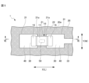
- FIG. 2 is a plan view showing the electronic component mounting structure according to the first embodiment.
- FIG. 3 is a cross-sectional view taken along line III-III in FIG.
- FIG. 4 is a partially enlarged cross-sectional view showing a main part of the electronic component mounting structure according to the first embodiment.
- FIG. 5 is a plan view showing a mounting structure of an electronic component according to the second embodiment.
- FIG. 6 is a cross-sectional view taken along line VI-VI in FIG.
- First Embodiment 1 shows a multilayer ceramic capacitor 10 as an electronic component applied to a mounting structure for an electronic component according to the first embodiment.
- the first embodiment is one form of a structure in which the multilayer ceramic capacitor 10 is mounted on a substrate.
- the multilayer ceramic capacitor 10 has an overall shape of a roughly rectangular parallelepiped.
- the multilayer ceramic capacitor 10 includes a component body 11 and a pair of external electrodes 16.
- the component body 11 has an inner layer portion 12 that is configured by alternately stacking a plurality of dielectric layers 121 and internal electrode layers 122.
- the direction in which the dielectric layers 121 and the internal electrode layers 122 are stacked is referred to as the "stacking direction T.”
- the direction perpendicular to the stacking direction T is referred to as the “length direction L.”
- the direction perpendicular to the stacking direction T and the length direction L is referred to as the "width direction W.”
- the pair of external electrodes 16 are aligned in the length direction L.
- the dimensions of the multilayer ceramic capacitor 10 include, for example, a length direction L of 0.2 mm or more and 1.7 mm or less, a width direction W of 0.12 mm or more and 0.9 mm or less, and a stacking direction T of 0.12 mm or more and 0.9 mm or less, but are not limited to these.
- the component body 11 has a generally rectangular parallelepiped shape.
- the component body 11 has a pair of main surfaces 17a that face each other in the stacking direction T, a pair of side surfaces 17b that face each other in the width direction W, and a pair of end surfaces 17c that face each other in the length direction L.
- the component body 11 has an inner layer portion 12 inside.
- the inner layer portion 12 has a multi-layer structure in which multiple internal electrode layers 122 and multiple dielectric layers 121 are alternately stacked in the stacking direction T.
- the four sides of the inner layer portion 12 on both sides in the width direction W and on both sides in the stacking direction T are covered with outer dielectric ceramic layers 13 made of the same material as the dielectric ceramic layers.
- the internal electrode layer 122 is formed from a metal material such as Ni, Cu, Ag, Pd, Ag-Pd alloy, Au, etc., but is not limited to these metal materials and may be formed from other conductive materials.
- the dielectric layer 121 and the outer dielectric ceramic layer 13 are formed by firing, for example, a ceramic material mainly composed of barium titanate or other ceramic material with a high dielectric constant (e.g., a material mainly composed of CaTiO3 , SrTiO3 , CaZrO3, etc.).
- a ceramic material mainly composed of barium titanate or other ceramic material with a high dielectric constant e.g., a material mainly composed of CaTiO3 , SrTiO3 , CaZrO3, etc.
- the pair of external electrodes 16 are respectively arranged at both ends of the component body 11 in the longitudinal direction L. Each external electrode 16 covers a pair of end faces 17c of the component body 11. The pair of external electrodes 16 may also be respectively arranged on a portion of a pair of main faces 17a or a portion of a pair of side faces 17b. In the multiple internal electrode layers 122 in the inner layer portion 12, one side of the internal electrode layers adjacent in the stacking direction T is connected to one external electrode 16, and the other side is connected to the other external electrode. Each of the pair of external electrodes 16 has an end face 16a in the longitudinal direction L.
- the external electrode 16 is composed of, for example, a laminated film of a sintered metal layer and a plating layer.
- the sintered metal layer is formed by baking a paste of, for example, Cu, Ni, Ag, Pd, Ag-Pd alloy, Au, or the like.
- the plating layer is composed of, for example, a Ni plating layer covered by a Sn plating layer.
- the multilayer ceramic capacitor 10 is manufactured, for example, by firing the component body 11 and then forming a pair of external electrodes 16 by baking, plating, or the like. In some cases, a portion of the external electrodes 16 is fired simultaneously with the component body 11, and then a plating layer of the external electrodes 16 is formed.
- the mounting structure 1 includes a substrate 20, a pair of lands 30 spaced apart from each other on the substrate 20, solder 40 disposed on each of the lands 30, and a multilayer ceramic capacitor 10.
- the multilayer ceramic capacitor 10 is mounted on the substrate 20 by soldering.
- the substrate 20 is formed in a sheet shape from an insulating material such as resin, glass, glass epoxy, paper phenol, ceramics, etc.
- Wiring 33 is formed on the surface 20a of the substrate 20.
- the wiring 33 is discontinuous with a separation section 21 in between, and a pair of lands 30, which are part of the wiring 33 and are connected to the external electrodes 16, are exposed on both sides of the separation section 21.
- the pair of lands 30 are spaced apart from each other and disposed on the surface 20a of the substrate 20. Therefore, the separation section 21 can also be considered the region between the pair of lands 30.
- Each of the pair of lands 30 is arranged in parallel so that the positions in the direction perpendicular to the direction in which the lands 30 are arranged are the same.
- the wiring 33 including the lands 30 is formed by depositing a highly conductive metal, such as Cu or Ag, on the surface 20a of the substrate 20.
- a highly conductive metal such as Cu or Ag
- Each of the pair of lands 30 has a rectangular shape in a plan view and has approximately the same shape and dimensions as each other.
- the direction perpendicular to the surface 20a of the substrate 20 is referred to as the "Z direction".
- the direction perpendicular to the Z direction and in which the pair of lands 30 are lined up is referred to as the "X direction”.
- the direction perpendicular to the X direction and the Z direction is referred to as the "Y direction”.
- the direction in which the pair of lands 30 are separated is referred to as the "separation direction”
- the direction in which the pair of lands 30 face each other is referred to as the "facing direction”.
- “land thickness” refers to the dimension of the land 30 in the Z direction.
- peripheral edges of the pair of lands 30 in the X and Y directions are referred to as the "periphery 31.”
- the edge of the peripheral edge 31 on the separation portion 21 side is referred to as the “inner edge 31a.”
- the inner edge 31a is a straight line extending in the Y direction.
- the surface 20a of the substrate 20 is covered with an insulating film 22.
- the insulating film 22 is made of an insulating material, for example, solder resist. However, this is not limited to this, and the insulating material that makes up the insulating film 22 can be an insulating coating material for substrates that is mainly composed of resin, such as polyolefin resin, acrylic resin, or polyurethane resin.
- the insulating film 22 extends onto each land 30, and a part of each land 30 near the peripheral portion 31 is covered with the insulating film 22.
- the peripheral portion 31 of each land 30 is covered with the insulating film 22.
- the surface 20a of the substrate 20 is covered with the insulating film 22.
- the part where the insulating film 22 is arranged is indicated by dot hatching.
- the portion of the insulating film 22 that is disposed on the surface of each land 30 is referred to as the "insulating film 22a," and the portion that is disposed in the region that overlaps with the separation portion 21 when viewed in the Z direction is referred to as the "insulating film 22b.”
- the insulating film 22 disposed in the separation portion 21 is included in the insulating film 22b.
- the inner edge 31a of the land 30 is an inclined surface that slopes toward the substrate 20 as it approaches the facing direction
- the insulating film 22 that is disposed in the region that overlaps with the inclined surface when viewed in the Z direction is included in the insulating film 22b, and is not included in the insulating film 22a.
- the "thickness of the insulating film 22" refers to the dimension of the insulating film 22 in the Z direction.
- the multilayer ceramic capacitor 10 mounted on the substrate 20 has a length direction L that is approximately along the X direction, a width direction W that is approximately along the Y direction, and a stacking direction T that is approximately along the Z direction. This causes one main surface 17a of the component body 11 to face the surface 20a of the substrate 20 approximately parallel. Note that the multilayer ceramic capacitor 10 does not necessarily have to be mounted on the substrate 20 with the main surface 17a facing the substrate 20, and may be mounted on the substrate 20 with one side surface 17b facing the substrate 20.
- one external electrode 16 is connected to one land 30 via solder 40, and the other external electrode 16 is connected to the other land 30 via solder 40.
- the end faces 16a of each external electrode 16 are almost all covered with solder 40. Note that each end face 16a of each external electrode 16 may be partially covered with solder 40.
- the multilayer ceramic capacitor 10 is positioned so that its center in the width direction W approximately coincides with the center in the width direction W of each land 30.
- the pair of external electrodes 16 each include a flat end face covering portion 16b that covers the end face 17c of the component body 11, and an extension portion 16c that extends from the end face covering portion 16b in the opposing direction and is disposed on a portion of the pair of main faces 17a and the pair of side faces 17b.
- the extension portion 16c covers only a portion of the end face 17c side of each of the main faces 17a and side faces 17b.
- the extension portion 16c is generally rectangular tubular.
- the end of the extension portion 16c on the opposing side forms the boundary portion between the external electrode 16 and the component body 11 (hereinafter referred to as "boundary portion 15").
- the extension portion 16c does not necessarily have to be generally rectangular tubular.
- the extension 16c does not need to extend to all of the main surfaces 17a and side surfaces 17b, but only needs to extend to at least one of the main surfaces 17a and side surfaces 17b that faces the substrate 20.
- the extension 16c covering one of the main surfaces 17a of the component body 11 facing the substrate 20 is connected to the land 30 via solder 40.
- the end (boundary 15) of the extension 16c on the opposing side is located in the direction away from the inner edge 31a of the land 30 connected to the extension 16c.
- the end (boundary 15) of the extension 16c on the opposing side may be located in the opposing direction from the inner edge 31a of the land 30 connected to the extension 16c or at approximately the same position as the inner edge 31a.
- the insulating film 22a may be located between the extension 16c and the land 30, or the insulating film 22a may not be provided.
- the insulating film 22b also fills the area between the substrate 20 and the component body 11 without leaving any gaps.
- the dimension of the insulating film 22 in the Z direction is the same as the distance between the substrate 20 and the component body 11.
- the insulating film 22b supports the component body 11 on the substrate 20.
- the insulating film 22b corresponds to a support member (more specifically, a first support member).
- the insulating film 22b may be provided so as to partially fill the area between the substrate 20 and the component body 11. That is, the area between the substrate 20 and the component body 11 may partially have an area where the insulating film 22 is not present. In this case, the insulating film 22a can also support the component body 11 on the land 30.
- the insulating film 22a is continuous with the insulating film 22b and extends from the insulating film 22b in the separation direction.
- the dimension of the insulating film 22a in the Z direction is the same as the separation dimension between the component body 11 and the land 30.
- the surfaces of the insulating films 22a and 22b (the surfaces on the side in the Z direction that are separated from the substrate 20) are flush with each other.
- the insulating film 22a supports the component body 11 on the land 30.
- the insulating film 22a corresponds to a support member (more specifically, a second support member).
- Each end of the insulating film 22a in the separation direction is in contact with the boundary portion 15.
- the boundary portion 15 is covered with the insulating film 22b.
- Each end of the insulating film 22b in the separation direction is an inclined surface, more specifically, an inclined surface that inclines toward the substrate 20 as it approaches the opposing direction.
- the insulating film 22a does not extend beyond the boundary portion 15 in the separation direction.
- each end of the insulating film 22a in the separation direction does not have to be in contact with the boundary portion 15.
- the insulating film 22a may not be present around the boundary portion 15 due to a gap or the like.
- the insulating film 22a may extend beyond the boundary portion 15 in the separation direction.
- the end of the solder 40 in the facing direction is in contact with the insulating film 22a.
- the end of the solder 40 on the facing side is an inclined surface, more specifically, an inclined surface that slopes away from the substrate 20 as it approaches the facing direction. Since the end of the insulating film 22a in the separating direction is an inclined surface that slopes toward the substrate 20 as it approaches the facing direction, it is possible to prevent the solder 40 from climbing up onto the insulating film 22a. Note that the end of the solder 40 in the facing direction does not have to be in contact with the insulating film 22a. In other words, there may be a gap or the like between the end of the solder 40 in the facing direction and the insulating film 22.
- solder 40 This allows the external electrode 16 to be firmly joined to the land 30.
- solder 40 there are no particular limitations on the type of solder 40 as long as it has properties that are compatible with each external electrode 16 and each land 30, and it may be, for example, Sn-Pb solder, Sn-Ag-Cu solder, Sn-Cu solder, Sn-Bi solder, etc.
- a gap GAP is formed between the land 30 and the extension 16c of the external electrode 16 that faces the land 30.
- the gap GAP can also be considered as the area sandwiched between the extension 16c and the land 30.
- the entire gap GAP overlaps with the component body 11 when viewed in the Z direction.
- the dimension of the gap GAP in the Z direction corresponds to the thickness of the insulating film 22b between the component body 11 and the substrate 20, and the thickness of the insulating film 22a between the component body 11 and the land 30.
- the dimension of the gap GAP in the Z direction can be adjusted by adjusting the thickness of the insulating film 22a and the thickness of the insulating film 22b.
- the solder 40 is placed in the gap Gap, and more specifically, fills the entire gap Gap without any gaps. Therefore, the Z-direction dimension of the gap Gap is the same as the Z-direction dimension of the solder 40 placed in the gap Gap.
- the "solder thickness" means the Z-direction dimension of the solder.
- the area between the extension 16c and the land 30 does not need to be filled with solder 40, and the solder 40 may be partially present, or may not be present. In this case, instead of the solder 40, a gap or an insulating film 22a may be present in the area between the extension 16c and the land 30.
- the thickness of the solder 40 arranged in the area (i.e., the gap) between the extension 16c and the land 30 is 1 ⁇ m or more and 100 ⁇ m or less. In this case, stress is less likely to be applied to the boundary portion 15, and the occurrence of cracks can be suppressed. In addition to stress caused by thermal shock, stress caused by bending of the substrate 20 can also be made less likely to act on the boundary portion 15.
- the contact area between the extension 16c and the solder 40 is relatively large.
- the thickness of the solder 40 within the above-mentioned range, it is possible to make it difficult for stress to be applied to the boundary portion 15, thereby suppressing the occurrence of cracks.
- the distance in the Z direction between the land 30 and the extension 16c is preferably 1 ⁇ m or more and 100 ⁇ m or less. Because the thickness of the solder 40 is determined according to the dimension of the gap GAP in the Z direction, this allows the thickness of the solder 40 to be adjusted to a suitable range.
- the thickness of the insulating film 22a is preferably adjusted so that the distance between the extension 16c and the land 30 is within the range of 1 ⁇ m to 100 ⁇ m.
- the thickness of the insulating film 22a is preferably in the range where the dimension obtained by subtracting the thickness of the land 30 and the extension 16c from the thickness of the insulating film 22b is 1 ⁇ m to 100 ⁇ m.
- the dimension of the gap Gap in the Z direction can be set to the desired dimension, and the thickness of the solder 40 placed in the gap Gap can also be set to the desired dimension.
- the thickness of the insulating film 22, the thickness of the land 30, and the thickness of the solder 40 arranged in the gap Gap are measured, for example, on a cross section obtained by cutting the mounting structure 1 parallel to the X and Z directions so as to pass through the center of the multilayer ceramic capacitor 1 in the Y direction.
- the thickness value of the solder 40 is determined, for example, by measuring the thickness of the solder 40 at multiple (e.g., three) positions on the cross section that are equally spaced in the X direction, and averaging the values obtained. The same applies to the insulating film 22 and the land 30.
- the boundary portion 15 is in contact with the insulating film 22a. This makes it possible to suppress contact between the boundary portion 15 and the solder 40. This makes it possible to suppress stress being applied to the boundary portion 15, thereby suppressing the occurrence of cracks.
- the soldering using the solder 40 is performed, for example, by reflow. That is, the multilayer ceramic capacitor 10 can be reflow mounted on the substrate 20.
- the mounting method of the multilayer ceramic capacitor 1 will be described below.
- an insulating film 22 is placed on the substrate 20.
- the insulating film 22 is placed so as to cover, for example, a portion of the land 30 including the peripheral portion 31.
- the thickness of the insulating film 22 is adjusted so that the dimension of the gap GAP in the Z direction is the desired dimension.
- a paste-like solder material is applied to the area of the land 30 that is not covered by the insulating film 22.
- the multilayer ceramic capacitor 1 is placed at a predetermined position on the land 30.
- the external electrode 16 sinks into the paste-like solder material until the component body 11 abuts against the insulating film 22a and the insulating film 22b.
- a gap GAP is formed between the extension portion 16c of the external electrode 16 and the land 30.
- the gap GAP is filled with the solder material. Part of the solder material is pushed out from between the extension portion 16c and the land 30 and wets up onto the end face covering portion 16b of the external electrode 16. In this state, the solder material solidifies, and the external electrode 16 and the land 30 are connected by the solder 40.
- the mounting structure 1 according to the first embodiment can provide the following advantages.
- the thickness of the solder 40 disposed in the area between the extension portion 16c and the land 30 is 1 ⁇ m or more and 100 ⁇ m or less.
- the distance in the Z direction between the land 30 and the extension portion 16c is 1 ⁇ m or more and 100 ⁇ m or less.
- an insulating film 22a is disposed in the region between the component body 11 and the land 30.
- the insulating film 22a supports the component body 11 on the land 30.
- an insulating film 22b is disposed in the region between the pair of lands 30 and the region formed when viewed in the Z direction.
- the insulating film 22b supports the component body 11 on the substrate 20.
- the Z-direction dimension of the gap GAP and the thickness of the solder 40 placed in the gap GAP can be adjusted to the desired dimensions.
- the thickness of the insulating film 22a is preferably adjusted so that the distance between the extension 16c and the land 30 is within the range of 1 ⁇ m to 100 ⁇ m.
- the thickness of the insulating film 22b is preferably set so that the distance between the extension 16c and the land 30 is within the range of 1 ⁇ m to 100 ⁇ m, as described above, with the thickness of the insulating film 22a being the thickness of the insulating film 22b minus the thickness of the land 30.
- the dimension of the gap GAP in the Z direction can be set in the range of 1 ⁇ m to 100 ⁇ m, and the thickness of the solder 40 placed in the gap GAP can be set in the range of 1 ⁇ m to 100 ⁇ m. This makes it possible to suppress the occurrence of cracks in the electronic component.
- a support member 50 is disposed between a pair of lands 30.
- the support member 50 is a member that supports the component body 11 on the substrate 20, and corresponds to a first support member.
- the support member 50 is disposed approximately in the center of the separation portion 21.
- the support member 50 includes a block member 51 that is generally rectangular parallelepiped-shaped.
- the block member 51 is formed, for example, from a metal, and more specifically, from copper foil.
- the block member 51 is formed from a material that has a higher melting point than solder.
- the block member 51 is disposed on the surface 20a of the substrate 20.
- the block member 51 is adhered to the surface 20a by, for example, an adhesive.
- the material of the block member 51 is not limited to metal.
- the block member 51 does not need to be made of a single material.
- the block member 51 may be made of multiple layers stacked together, each layer being made of a different material.
- the surface of the separation portion 21 is covered with an insulating film 22b made of solder resist.
- the insulating film 22b is formed as a thin film, and is thinner than in the first embodiment. Therefore, there is a space in the area between the substrate 20 and the component body 11 where no solder resist is arranged. In this way, the insulating film 22b does not necessarily have to fill the area between the substrate 20 and the component body 11 without any gaps.
- the insulating film 22b covers the surface of the block member 51. Therefore, the support member 50 is configured to include the block member 51 and a resist film portion 52 that covers the surface of the block member 51. Silk may further be applied to the surface of the resist film portion 52. Note that the block member 51 does not necessarily have to be covered with the insulating film 22, and the resist film portion 52 is not an essential component of the support member 50.
- the support member 50 is tightly sandwiched between the component body 11 and the substrate 20.
- the Z-direction dimension of the support member 50 is greater than the thickness of the land 30.
- the insulating film 22 is not disposed between the land 30 and the extension 16c. Therefore, the separation distance between the component body 11 and the substrate 20 is the same as the Z-direction dimension of the support member 50.
- a gap GAP is formed between the component body 11 and the land 30.
- the Z-direction dimension of the gap GAP is the same as the dimension obtained by subtracting the thickness of the land 30 from the Z-direction dimension of the support member 50. Therefore, by adjusting the Z-direction dimension of the support member 50, the Z-direction dimension of the gap GAP can be adjusted. And the thickness of the solder 40 disposed in the gap GAP can be adjusted.
- the Z-direction dimension of the support member 50 arranged in the separation portion 21 is preferably set so that the separation dimension between the extension portion 16c and the land 30 is within the range of 1 ⁇ m to 100 ⁇ m.
- the thickness of the solder 40 arranged in the gap Gap can be set to 1 ⁇ m to 100 ⁇ m. This makes it possible to suppress the occurrence of cracks in the multilayer ceramic capacitor 1.
- the solder 40 extends to the inner edge 31a of the land 30 and covers the end of the extension 16c in the opposing direction. Even in this configuration, the occurrence of cracks can be sufficiently suppressed by keeping the thickness of the solder 40 within the above range.
- the position where the support member 50 can be placed is not limited to on the separation portion 21.
- the support member 50 may be placed in the gap Gap, and the block member 51 may be placed on the land 30.
- the Z-direction dimension of the support member 50 placed in the gap Gap is 1 ⁇ m or more and 100 ⁇ m or less. This allows the thickness of the solder 40 placed in the gap Gap to be within the desired range.
- the end of the insulating film 22a in the separation direction extends to a position where it contacts the end of the extension portion 16c in the opposing direction, but the insulating film 22a may extend further in the separation direction than the boundary portion 15.
- the insulating film 22a may be disposed in the region sandwiched between the extension portion 16c and the land 30, and the region sandwiched between the extension portion 16c and the land 30 does not have to be filled with the solder 40 over the entire area. In that case, the distance between the solder 40 and the boundary portion 15 can be made larger, so that the solder 40 can be more effectively prevented from contacting the boundary portion 15.
- the configuration of the first embodiment is preferable in that the external electrode 16 can be firmly soldered to the land 30.
- the support member 50 is not limited to the configuration of the second embodiment described above, so long as it is possible to maintain a distance between the extension 16c of the external electrode 16 and the substrate 20.
- the support member may be, for example, an adhesive.
- the adhesive may be, for example, an epoxy-based resin adhesive.
- the support member 50 is formed from a material that has a higher melting point than solder. Furthermore, the solder that connects the external electrode and the land is not considered to be a support member.
- the multilayer ceramic capacitor 10 in the above embodiment is an example of an electronic component, but the electronic component is not limited to this, and other two-terminal electronic components such as inductors are also applicable.
- the component body is made of magnetic ceramics, etc.
- the present invention also includes the following combinations:
- An electronic component comprising: a pair of lands arranged on a substrate with a space between them; solder arranged on each of the lands; a component body having laminated dielectric layers and internal electrode layers, the component body including a pair of main surfaces facing each other in a stacking direction, a pair of side surfaces facing each other in a width direction perpendicular to the stacking direction, and a pair of end surfaces facing each other in a length direction perpendicular to the stacking direction and the width direction; and a pair of external electrodes arranged on each of the end surfaces, each of the external electrodes being connected to each of the lands via the solder; each of the external electrodes including an extension portion extending to at least a part of each of the main surfaces and each of the side surfaces; and when the direction perpendicular to the surface of the substrate is defined as the Z direction, the dimension of the solder arranged in the region between the land and the extension portion in the Z direction is 1 ⁇ m or more and 100 ⁇ m or less.
- ⁇ 2> The mounting structure described in ⁇ 1>, in which at least one of the substrate and the land is provided with a support member that supports the component body.
- ⁇ 4> The electronic component mounting structure described in ⁇ 2> or ⁇ 3>, in which the support member has a first support member arranged in the region between the pair of lands, and the Z-direction dimension of the first support member is in the range of 1 ⁇ m or more and 100 ⁇ m or less, obtained by subtracting the Z-direction dimension of the land from the Z-direction dimension of the first support member.
- ⁇ 5> An electronic component mounting structure described in any one of ⁇ 2> to ⁇ 4>, in which the support member has a second support member arranged in a region between the land and the extension, and the dimension of the second support member in the Z direction is 1 ⁇ m or more and 100 ⁇ m or less.
- An electronic component mounting structure comprising: a pair of lands arranged on a substrate with a space between them; solder arranged on each of the lands; a component body having laminated dielectric layers and internal electrode layers, the component body including a pair of main surfaces facing each other in a stacking direction, a pair of side surfaces facing each other in a width direction perpendicular to the stacking direction, and a pair of end surfaces facing each other in a length direction perpendicular to the stacking direction and the width direction; and external electrodes arranged on each of the end surfaces, the external electrodes being connected to the lands via the solder, each of the external electrodes including an extension portion extending to at least a part of each of the main surfaces and each of the side surfaces, and when a direction substantially perpendicular to the surface of the substrate is defined as a Z direction, the distance in the Z direction between the land and the extension portion is 1 ⁇ m or more and 100 ⁇ m or less
- Multilayer ceramic capacitor (electronic component) REFERENCE SIGNS LIST 11 Component body 16 External electrode 16b End surface covering portion 16c Extension portion 17a Main surface 17b Side surface 17c End surface 20 Substrate 22a Insulating film (second supporting member and insulating material) 22b Insulating film (first support member and insulating material) 30 Land 40 Solder 50 Support member (first support member) 51 Block member (first support member) 52 Resist film portion (first support member and insulating material) 121 Dielectric layer 122 Internal electrode layer
Landscapes
- Engineering & Computer Science (AREA)
- Power Engineering (AREA)
- Microelectronics & Electronic Packaging (AREA)
- Fixed Capacitors And Capacitor Manufacturing Machines (AREA)
Priority Applications (1)
| Application Number | Priority Date | Filing Date | Title |
|---|---|---|---|
| JP2025556197A JPWO2025099997A1 (https=) | 2023-11-07 | 2024-07-19 |
Applications Claiming Priority (2)
| Application Number | Priority Date | Filing Date | Title |
|---|---|---|---|
| JP2023190269 | 2023-11-07 | ||
| JP2023-190269 | 2023-11-07 |
Publications (1)
| Publication Number | Publication Date |
|---|---|
| WO2025099997A1 true WO2025099997A1 (ja) | 2025-05-15 |
Family
ID=95695392
Family Applications (1)
| Application Number | Title | Priority Date | Filing Date |
|---|---|---|---|
| PCT/JP2024/025904 Pending WO2025099997A1 (ja) | 2023-11-07 | 2024-07-19 | 電子部品の実装構造 |
Country Status (2)
| Country | Link |
|---|---|
| JP (1) | JPWO2025099997A1 (https=) |
| WO (1) | WO2025099997A1 (https=) |
Citations (7)
| Publication number | Priority date | Publication date | Assignee | Title |
|---|---|---|---|---|
| JPH1140918A (ja) * | 1997-07-22 | 1999-02-12 | Taiyo Yuden Co Ltd | セラミックス素子、部品実装基板及び配線基板 |
| US6903920B1 (en) * | 2004-08-06 | 2005-06-07 | Kemet Electronics | Clip-on leadframe for large ceramic SMD |
| JP2013065820A (ja) * | 2011-09-01 | 2013-04-11 | Murata Mfg Co Ltd | 実装構造 |
| JP2013122939A (ja) * | 2011-12-09 | 2013-06-20 | Sony Corp | 回路基板 |
| WO2016017634A1 (ja) * | 2014-07-30 | 2016-02-04 | 京セラ株式会社 | 積層型電子部品およびその実装構造体 |
| US20210217559A1 (en) * | 2020-01-15 | 2021-07-15 | Samsung Electro-Mechanics Co., Ltd. | Multilayered electronic component and board having the same mounted thereon |
| JP2023053630A (ja) * | 2021-10-01 | 2023-04-13 | 株式会社村田製作所 | 電子部品の実装構造 |
-
2024
- 2024-07-19 WO PCT/JP2024/025904 patent/WO2025099997A1/ja active Pending
- 2024-07-19 JP JP2025556197A patent/JPWO2025099997A1/ja active Pending
Patent Citations (7)
| Publication number | Priority date | Publication date | Assignee | Title |
|---|---|---|---|---|
| JPH1140918A (ja) * | 1997-07-22 | 1999-02-12 | Taiyo Yuden Co Ltd | セラミックス素子、部品実装基板及び配線基板 |
| US6903920B1 (en) * | 2004-08-06 | 2005-06-07 | Kemet Electronics | Clip-on leadframe for large ceramic SMD |
| JP2013065820A (ja) * | 2011-09-01 | 2013-04-11 | Murata Mfg Co Ltd | 実装構造 |
| JP2013122939A (ja) * | 2011-12-09 | 2013-06-20 | Sony Corp | 回路基板 |
| WO2016017634A1 (ja) * | 2014-07-30 | 2016-02-04 | 京セラ株式会社 | 積層型電子部品およびその実装構造体 |
| US20210217559A1 (en) * | 2020-01-15 | 2021-07-15 | Samsung Electro-Mechanics Co., Ltd. | Multilayered electronic component and board having the same mounted thereon |
| JP2023053630A (ja) * | 2021-10-01 | 2023-04-13 | 株式会社村田製作所 | 電子部品の実装構造 |
Also Published As
| Publication number | Publication date |
|---|---|
| JPWO2025099997A1 (https=) | 2025-05-15 |
Similar Documents
| Publication | Publication Date | Title |
|---|---|---|
| KR102443777B1 (ko) | 칩형 전자 부품 | |
| KR20250052344A (ko) | 적층 세라믹 콘덴서 | |
| JP5958479B2 (ja) | 電子部品の実装構造体 | |
| KR20200125456A (ko) | 칩형 전자부품 및 전자부품의 실장 구조체 | |
| US10790092B2 (en) | Multilayer ceramic electronic component | |
| CN101944435A (zh) | 电子元件 | |
| JP6962305B2 (ja) | 積層セラミック電子部品 | |
| JP2017157805A (ja) | 電子部品の実装構造及びその電子部品の製造方法 | |
| US20240321521A1 (en) | Electronic component | |
| KR102562428B1 (ko) | 적층 세라믹 전자부품 | |
| JP3535998B2 (ja) | 積層セラミック電子部品 | |
| KR20250044355A (ko) | 칩형 전자부품 | |
| US10650972B2 (en) | Electronic component | |
| JP2004296936A (ja) | セラミック電子部品 | |
| US12267956B2 (en) | Mounting structure of electronic component | |
| WO2025099997A1 (ja) | 電子部品の実装構造 | |
| JP2005294618A (ja) | 電子部品 | |
| WO2025142038A1 (ja) | 電子部品の実装構造 | |
| US12230448B2 (en) | Electronic component with metal terminal, connection structure, and method for manufacturing connection structure | |
| US12444534B2 (en) | Mounting structure and mounting method of electronic component | |
| US20250095920A1 (en) | Electronic component | |
| JP7468341B2 (ja) | 電子部品 | |
| JP2026058006A (ja) | 積層セラミック電子部品 | |
| KR20250038729A (ko) | 전자부품 및 전자부품의 실장 구조 | |
| KR20250073405A (ko) | 적층 세라믹 전자부품 |
Legal Events
| Date | Code | Title | Description |
|---|---|---|---|
| 121 | Ep: the epo has been informed by wipo that ep was designated in this application |
Ref document number: 24888299 Country of ref document: EP Kind code of ref document: A1 |
|
| ENP | Entry into the national phase |
Ref document number: 2025556197 Country of ref document: JP Kind code of ref document: A |