WO2025094656A1 - 半導体装置、半導体装置の製造方法、および電力変換装置 - Google Patents
半導体装置、半導体装置の製造方法、および電力変換装置 Download PDFInfo
- Publication number
- WO2025094656A1 WO2025094656A1 PCT/JP2024/036671 JP2024036671W WO2025094656A1 WO 2025094656 A1 WO2025094656 A1 WO 2025094656A1 JP 2024036671 W JP2024036671 W JP 2024036671W WO 2025094656 A1 WO2025094656 A1 WO 2025094656A1
- Authority
- WO
- WIPO (PCT)
- Prior art keywords
- heat sink
- heat
- semiconductor device
- heat sinks
- housing
- Prior art date
- Legal status (The legal status is an assumption and is not a legal conclusion. Google has not performed a legal analysis and makes no representation as to the accuracy of the status listed.)
- Pending
Links
Images







Classifications
-
- H—ELECTRICITY
- H05—ELECTRIC TECHNIQUES NOT OTHERWISE PROVIDED FOR
- H05K—PRINTED CIRCUITS; CASINGS OR CONSTRUCTIONAL DETAILS OF ELECTRIC APPARATUS; MANUFACTURE OF ASSEMBLAGES OF ELECTRICAL COMPONENTS
- H05K7/00—Constructional details common to different types of electric apparatus
- H05K7/20—Modifications to facilitate cooling, ventilating, or heating
-
- H—ELECTRICITY
- H10—SEMICONDUCTOR DEVICES; ELECTRIC SOLID-STATE DEVICES NOT OTHERWISE PROVIDED FOR
- H10W—GENERIC PACKAGES, INTERCONNECTIONS, CONNECTORS OR OTHER CONSTRUCTIONAL DETAILS OF DEVICES COVERED BY CLASS H10
- H10W40/00—Arrangements for thermal protection or thermal control
- H10W40/10—Arrangements for heating
-
- H—ELECTRICITY
- H10—SEMICONDUCTOR DEVICES; ELECTRIC SOLID-STATE DEVICES NOT OTHERWISE PROVIDED FOR
- H10W—GENERIC PACKAGES, INTERCONNECTIONS, CONNECTORS OR OTHER CONSTRUCTIONAL DETAILS OF DEVICES COVERED BY CLASS H10
- H10W40/00—Arrangements for thermal protection or thermal control
- H10W40/40—Arrangements for thermal protection or thermal control involving heat exchange by flowing fluids
- H10W40/43—Arrangements for thermal protection or thermal control involving heat exchange by flowing fluids by flowing gases, e.g. forced air cooling
Definitions
- This disclosure relates to a semiconductor device, a method for manufacturing a semiconductor device, and a power conversion device.
- the housing has been proposed to include an external frame, an opening formed to penetrate the interior of the external frame, and at least one bridge provided on the external frame to separate the opening and support the modular cooling device inserted into the opening (see, for example, Patent Document 1).
- the semiconductor device also includes at least one airflow guide member that is inserted between the multiple modular cooling devices and controls the flow of air into the modular cooling device.
- heat generated from the semiconductor elements of one semiconductor module is dissipated by each heat sink, and the heated air flows into the heat sinks of the other semiconductor modules, raising the temperatures reached by the other semiconductor modules.
- the rise in temperature reached by the semiconductor module located furthest downwind is particularly significant. This causes thermal interference between the semiconductor modules within the semiconductor device. To avoid this thermal interference, it was necessary to enlarge the heat sinks.
- the present disclosure therefore aims to provide technology that reduces the temperature reached by a semiconductor module placed on the most downwind side and enables the heat sink to be made smaller.
- the semiconductor device comprises a housing, a mounting plate fixed within the housing and having a plurality of openings, a plurality of heat sinks respectively attached to the plurality of openings of the mounting plate, a plurality of semiconductor modules respectively mounted on the plurality of heat sinks, and a cooling fan provided in the housing for blowing air to the plurality of heat sinks, the plurality of heat sinks being arranged along a first direction parallel to the blowing direction of the cooling fan, and the dimension in a second direction perpendicular to the first direction of the heat sink arranged on the windward side among the plurality of heat sinks being smaller than the dimension in the second direction of the heat sink arranged on the downwind side.
- air with a small temperature rise that passes through a space where a heat sink arranged on the windward side is not arranged flows into a heat sink arranged on the downwind side, thereby reducing the temperature reached by a semiconductor module mounted on a heat sink arranged on the downwind side.
- FIG. 1 is a top view of a semiconductor device according to a first embodiment
- FIG. 2 is a cross-sectional view of a heat sink integrated semiconductor module.
- FIG. 2 is a cross-sectional view of a heat sink integrated semiconductor module.
- FIG. 2 is a cross-sectional view of a heat sink integrated semiconductor module.
- 1 is a bottom view of a semiconductor device according to a first embodiment
- 4 is a contour diagram illustrating the temperature of air flowing between heat dissipation fins included in the semiconductor device according to the first embodiment
- FIG. FIG. 11 is a cross-sectional view showing another example of a semiconductor module.
- FIG. 11 is a cross-sectional view showing another example of a semiconductor module.
- FIG. 11 is a cross-sectional view showing another example of a semiconductor module.
- FIG. 11 is a cross-sectional view showing another example of a semiconductor module.
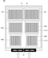
- FIG. 13 is a bottom view of a semiconductor device according to a modification of the first embodiment.
- FIG. 11 is a cross-sectional view of a semiconductor device according to a modification of the first embodiment. 13 is a contour diagram illustrating the temperature of air flowing between heat dissipation fins included in the semiconductor device according to the modification of the first embodiment.
- FIG. 5A to 5C are cross-sectional views showing a manufacturing method of a heat sink-integrated semiconductor module included in the semiconductor device according to the first embodiment.
- 5A to 5C are cross-sectional views showing a manufacturing method of a heat sink-integrated semiconductor module included in the semiconductor device according to the first embodiment.
- FIG. 11 is a top view of a semiconductor device according to a second embodiment.
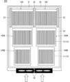
- FIG. 11 is a bottom view of a semiconductor device according to a second embodiment. 13 is a contour diagram illustrating the temperature of air flowing between heat dissipation fins included in the semiconductor device according to the second embodiment.
- FIG. FIG. 13 is a bottom view of a semiconductor device according to a modification of the second embodiment.
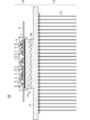
- FIG. 11 is a top view of a semiconductor device according to a third embodiment. This is a cross-sectional view of line AA in Figure 19.
- 13 is a block diagram showing a configuration of a power conversion system to which a power conversion device according to a fourth embodiment is applied.
- Fig. 1 is a top view of a semiconductor device 202 according to the first embodiment.
- Fig. 2 is a cross-sectional view of a heat sink integrated semiconductor module 100.
- Fig. 3 is a cross-sectional view of a heat sink integrated semiconductor module 100A.
- Fig. 4 is a cross-sectional view of a heat sink integrated semiconductor module 100B.
- Fig. 5 is a bottom view of the semiconductor device 202 according to the first embodiment.
- the semiconductor device 202 includes a housing 20, a mounting plate 21, a plurality of (e.g., six) heat sink-integrated semiconductor modules 100, 100A, and 100B, and a cooling fan 22.
- the housing 20 is formed into a rectangular frame shape when viewed from above.
- the mounting plate 21 is formed into a rectangular shape when viewed from above, and is fixed inside the housing 20.
- the mounting plate 21 is provided with a plurality of (e.g., six) openings (not shown) to which the heat sinks 13 of the plurality of heat sink-integrated semiconductor modules 100, 100A, 100B are respectively attached.
- Two cooling fans 22 are provided on one of the short sides (the lower side in FIG. 1) of the housing 20.
- the cooling fans 22 blow air to the heat sinks 13 of the plurality of heat sink-integrated semiconductor modules 100, 100A, 100B.
- the cooling fans 22 blow air in the direction of the arrow in FIG. 1 (the direction from the bottom to the top in FIG. 1).
- the heat sink integrated semiconductor modules 100, 100A, 100B are arranged in two rows along a first direction parallel to the airflow direction of the cooling fan 22, and in each row, the heat sink integrated semiconductor modules 100B, 100A, 100 are arranged in this order from the windward side to the leeward side.
- the windward side is the lower side in FIG. 1
- the leeward side is the upper side in FIG. 1.
- the heat sink integrated semiconductor module 100 includes a semiconductor module 10 and a heat sink 13.
- the semiconductor module 10 includes multiple semiconductor elements 1, a metal conductor 4 such as a lead frame, an insulating material 5 such as an insulating sheet, a fin base 9, a sealing material 7 such as an epoxy resin, multiple control terminals 6, and multiple main terminals 8.
- semiconductor elements 1 are mounted on the upper surface of a metal conductor 4 via a bonding material 2 such as solder.
- the semiconductor elements 1 and the metal conductor 4, and the semiconductor elements 1 themselves, are connected by wiring 3.
- the semiconductor elements 1 are Si-based semiconductor elements, SiC-based semiconductor elements, or compound semiconductor elements such as GaN.
- the metal conductor 4 is arranged via an insulating material 5 attached to the upper surface of the fin base 9.
- the sealing material 7 seals the multiple semiconductor elements 1, the metal conductor 4, the insulating material 5, and the fin base 9 so that the multiple main terminals 8, which are part of the metal conductor 4, and the underside of the fin base 9 are exposed.
- the heat sink 13 has a heat sink base 11 that is integrated with the underside of the fin base 9, and a number of heat dissipation fins 12 that protrude downward from the heat sink base 11 (the side opposite the fin base 9).
- a first uneven portion 9a is provided on the underside of the fin base 9.
- a second uneven portion 11a that can fit into the first uneven portion 9a is provided on the upper surface of the heat sink base 11 (the surface facing the fin base 9) except for the outer periphery.
- the fin base 9 and heat sink 13 are integrated by fitting the first uneven portion 9a and the second uneven portion 11a together by pressing. This makes it possible to realize a grease-free heat sink integrated semiconductor module 100. Because the heat sink integrated semiconductor module 100 does not use thermal conductive grease, it has low thermal resistance and excellent long-term reliability.
- the fin base 9 is manufactured by cutting, forging, casting, extrusion, or the like, and is made of aluminum or an aluminum alloy. However, the material of the fin base 9 is not limited to aluminum material, and may be copper, etc.
- the heat sink 13 is a crimped heat sink in which the heat sink base 11 and the heat dissipation fins 12 are integrated by crimping.
- the heat sink base 11 of the crimped heat sink is made by cutting, die casting, forging, extrusion, or the like, and is made of aluminum or an aluminum alloy.
- the heat sink base 11 of the crimped heat sink and the heat dissipation fins 12 of the crimped heat sink are not limited to being made of aluminum material, and they may be made of a combination of different materials.
- the heat dissipation capacity is further improved compared to aluminum-based materials.
- the heat sink 13 When a crimped heat sink, in which the heat sink base 11 and heat dissipation fins 12 are integrated by crimping, is used as the heat sink 13, there are no processing constraints (aspect ratio) such as those of die casting, forging, or extrusion, so the heat dissipation fins 12 can be designed freely and the heat dissipation capacity of the heat sink 13 can be improved.
- the heat sink 13 is not limited to a crimped heat sink, and the same effect can be obtained with a heat sink made by cutting, forging, extrusion, casting, or other processes.
- a mounting plate 21 having an opening in an area corresponding to the heat dissipation fins 12 of the heat sink 13 is fixed inside the housing 20, and the heat sink integrated semiconductor modules 100, 100A, and 100B are attached and fixed to the opening of the mounting plate 21 to complete the semiconductor device 202.
- the dimension in a second direction perpendicular to the first direction of the heat sink 13 arranged on the windward side is smaller than the dimension in the second direction of the heat sink 13 arranged on the leeward side.
- the second direction is the left-right direction in FIG. 1.
- the dimension in the second direction of the heat sink 13 of the heat sink-integrated semiconductor module 100B arranged on the windward side is smaller than the dimension in the second direction of the heat sink 13 of the heat sink-integrated semiconductor module 100A arranged on the leeward side.
- the dimension in the second direction of the heat sink 13 of the heat sink-integrated semiconductor module 100A arranged on the windward side is smaller than the dimension in the second direction of the heat sink 13 of the heat sink-integrated semiconductor module 100 arranged on the leeward side.
- the dimension in the second direction of the heat sink 13 is smaller from the leeward side to the windward side.
- the dimension in the first direction of the heat sink 13 of the heat sink-integrated semiconductor modules 100, 100A, and 100B is the same.
- the number of heat dissipation fins 12 is set according to the dimension of the heat sink 13 in the second direction. In other words, from the downwind side to the upwind side, the number of heat dissipation fins 12 decreases and the area without heat dissipation fins 12 in the housing 20 increases. Also, as shown in Figure 1, the central axes 31 in the first direction of each heat sink 13 in each row are aligned. Here, the central axis 31 in the first direction refers to the axis extending in the first direction that passes through the center in the second direction.
- Figure 6 is a contour diagram that shows a schematic diagram of the temperature of the air flowing between the heat dissipation fins 12 provided in the semiconductor device according to the first embodiment.
- Reference numeral 32 indicates a temperature contour.
- the dimension in the second direction of the heat sink 13 arranged on the windward side is smaller than the dimension in the second direction of the heat sink 13 arranged on the downwind side, so that air with a small temperature rise that passes through the part on the upwind side where there are no heat dissipation fins 12 flows between the heat dissipation fins 12 of the heat sink 13 arranged on the downwind side.
- FIGS. 7 to 9 are cross-sectional views showing other examples of the semiconductor module 10.
- the semiconductor module 10 has a metal plate 15 instead of the fin base 9.
- the main terminal 8 is bent upward.
- the semiconductor module 10 has a metal plate 15 instead of the fin base 9, and a resin case 17 arranged to surround the peripheral portion of the metal plate 15 is filled with a sealing material 7.
- the heat sink 13 is not limited to a crimped heat sink, and the same effect can be obtained with a heat sink made by cutting, forging, extrusion, casting, or other processes.
- FIG. 10 is a bottom view of the semiconductor device 202 according to the modified example of the first embodiment.
- FIG. 11 is a cross-sectional view of the semiconductor device 202 according to the modified example of the first embodiment. Specifically, it is a cross-sectional view of a portion of the semiconductor device 202 according to the modified example of the first embodiment where the heat sink integrated semiconductor module 100 is arranged.
- FIG. 12 is a contour diagram that shows the temperature of the air flowing between the heat dissipation fins 12 provided in the semiconductor device 202 according to the modified example of the first embodiment.
- structural support members 23 are placed between the heat sinks 13 of adjacent heat sink-integrated semiconductor modules 100 arranged on the most downwind side, and between the housing 20 and the heat sink 13 of the heat sink-integrated semiconductor module 100 arranged on the most downwind side, as shown in Figures 10 and 11.
- the flow rate of the air flowing between the heat dissipation fins 12 of the heat sink integrated semiconductor module 100 arranged on the most downwind side is further increased.
- the heat dissipation performance of the heat sink 13 is further improved, and as shown in FIG. 12, it is possible to further reduce the temperature reached by the heat sink integrated semiconductor module 100 arranged on the most downwind side.
- the structural support member 23 it is possible to suppress bending of the mounting plate 21 to which the heat sink integrated semiconductor modules 100, 100A, 100B are attached. If the mounting plate 21 bends, not only will it be impossible to fix the housing 20 and the mounting plate 21, but the stress on each part due to vibrations during use of the product will increase, which may increase the rate of product failure, but it is possible to avoid these problems.
- Fig. 13 is a cross-sectional view showing a method for manufacturing the heatsink-integrated semiconductor module 100B included in the semiconductor device 202 according to the first embodiment.
- Fig. 14 is a cross-sectional view showing a method for manufacturing the heatsink-integrated semiconductor module 100 included in the semiconductor device according to the first embodiment. Since the manufacturing method of the heatsink-integrated semiconductor modules 100, 100A, and 100B is the same, only the manufacturing method of the heatsink-integrated semiconductor modules 100 and 100B will be described here.
- a semiconductor element 1 is mounted on a fin base 9, and a semiconductor module 10 is formed in which the semiconductor element 1 is sealed with a sealing material 7 in such a manner that the first uneven portion 9a of the fin base 9 opposite the side on which the semiconductor element 1 is mounted is exposed.
- a heat sink 13 is prepared in which a second uneven portion 11a that fits into the first uneven portion 9a is formed on the heat sink base 11, and multiple heat dissipation fins 12 are integrated with the heat sink base 11 by crimping on the side opposite the second uneven portion 11a. Furthermore, a crimping blade unit 30 is prepared as a jig that is inserted between the multiple heat dissipation fins 12 of the heat sink 13 and has multiple crimping blades that receive a press load.
- the heat sink 13 is mounted on the crimping blade unit 30, and the semiconductor module 10, which has been integrated with the sealing material 7 exposing the first uneven portion 9a of the fin base 9, is set on the second uneven portion 11a of the heat sink 13 and a press load is applied to integrate the fin base 9 of the semiconductor module 10 with the heat sink 13.
- the crimping blade unit 30 only needs to support the area of the heat sink 13 that corresponds to the semiconductor module 10, so the same crimping blade unit 30 can be used even if the dimensions of the heat sink base 11 of the heat sink 13 increase and the number of heat dissipation fins 12 increases. This makes it possible to reduce the temperature reached by the heat sink-integrated semiconductor module 100 located on the most downwind side without reducing productivity.
- the semiconductor device 202 includes a housing 20, a mounting plate 21 fixed inside the housing 20 and having a plurality of openings, a plurality of heat sinks 13 attached to the plurality of openings of the mounting plate 21, a plurality of semiconductor modules 10 mounted on the plurality of heat sinks 13, and a cooling fan 22 provided in the housing 20 for blowing air to the plurality of heat sinks 13.
- the plurality of heat sinks 13 are arranged along a first direction parallel to the air blowing direction of the cooling fan 22, and the dimension in a second direction perpendicular to the first direction of the heat sink 13 arranged on the windward side among the plurality of heat sinks 13 is smaller than the dimension in the second direction of the heat sink 13 arranged on the downwind side.
- each semiconductor module 10 is a heat sink integrated semiconductor module 100, 100A, 100B that is integrally configured with each heat sink 13.
- the heat sinks 13 are arranged in two rows along the first direction, and the central axes 31 of the heat sinks 13 in each row in the first direction are aligned.
- changing the dimension of the heat sink 13 in the second direction between the upwind side and the downwind side is synonymous with changing the dimension of the heat sink 13 in the second direction for each of the U-phase, V-phase, and W-phase of the semiconductor device. Therefore, by visually inspecting the heat sink 13, it is easy to recognize in which phase the heat sink-integrated semiconductor modules 100, 100A, 100B have been used or are planned to be used. This improves the productivity and workability of the semiconductor device.
- structural support members 23 are provided between adjacent heat sinks 13 arranged on the most downwind side, and between the housing 20 and the heat sink 13 arranged on the most downwind side. This makes it possible to further reduce the temperature reached by the heat sink-integrated semiconductor module 100 arranged on the most downwind side. In addition, it is possible to suppress bending of the mounting plate 21 to which the heat sink-integrated semiconductor modules 100, 100A, 100B are attached.
- the heat sink integrated semiconductor modules 100, 100A, and 100B do not use thermal conductive grease, so they have low thermal resistance and excellent long-term reliability.
- a semiconductor device 202 according to a second embodiment will be described.
- Fig. 15 is a top view of the semiconductor device 202 according to the second embodiment.
- Fig. 16 is a bottom view of the semiconductor device 202 according to the second embodiment.
- Fig. 17 is a contour diagram showing the temperature of air flowing between the heat dissipation fins 12 included in the semiconductor device 202 according to the second embodiment. Note that in the second embodiment, the same components as those described in the first embodiment are denoted by the same reference numerals and description thereof will be omitted.
- the central axis 31 in the first direction of each heat sink 13 in each row is aligned
- the central axis 31 in the first direction of at least one heat sink 13 in each row is misaligned
- the two heat sink integrated semiconductor modules 100A, 100B are arranged such that the central axis 31 in the first direction of the heat sink 13 of the two heat sink integrated semiconductor modules 100A, 100B is misaligned with the central axis 31 in the first direction of the heat sink integrated semiconductor module 100 in each row.
- the heat generated by the multiple semiconductor elements 1 mounted on the heat sink-integrated semiconductor modules 100, 100A, 100B is transferred through the bonding material 2, the metal conductor 4, the insulating material 5, and the fin base 9, and is dissipated from the heat dissipation fins 12. For this reason, the temperature is highest near the center of the fin base 9 in the second direction, and the temperature of the air flowing between the heat dissipation fins 12 is also high near the center of the fin base 9 in the second direction.
- the temperature reached by the heat sink-integrated semiconductor module 100 arranged on the most downwind side can be reduced.
- the central axes 31 in the second direction of the heat sink-integrated semiconductor modules 100, 100A, and 100B are shifted by at least one to reduce the temperature of the air flowing into the heat dissipation fins 12 and reduce the temperature reached by the heat sink-integrated semiconductor module 100 arranged on the most downwind side.
- Figure 18 is a bottom view of a semiconductor device 202 according to a modified example of the second embodiment.
- structural support members 23 may be arranged between the heat sinks 13 of adjacent heat sink-integrated semiconductor modules 100 arranged on the most downwind side, and between the housing 20 and the heat sink 13 of the heat sink-integrated semiconductor module 100 arranged on the most downwind side.
- the multiple heat sinks 13 are arranged in two rows along the first direction, and the central axis 31 in the first direction of at least one heat sink 13 in each row is offset.
- structural support members 23 are provided between adjacent heat sinks 13 arranged on the most downwind side, and between the housing 20 and the heat sink 13 arranged on the most downwind side. This makes it possible to further reduce the temperature reached by the heat sink-integrated semiconductor module 100 arranged on the most downwind side. In addition, it is possible to suppress bending of the mounting plate 21 to which the heat sink-integrated semiconductor modules 100, 100A, 100B are attached.
- Fig. 19 is a top view of the semiconductor device 202 according to the third embodiment.
- Fig. 20 is a cross-sectional view taken along line A-A in Fig. 19. Note that in the third embodiment, the same components as those described in the first and second embodiments are denoted by the same reference numerals, and description thereof will be omitted.
- the second direction dimension of the heat sink 13 arranged on the windward side among the multiple heat sinks 13 is smaller than the second direction dimension of the heat sink 13 arranged on the leeward side.
- the first direction dimension of the heat sink 13 arranged on the windward side among the multiple heat sinks 13 is smaller than the first direction dimension of the heat sink 13 arranged on the leeward side.
- the dimension in the first direction of the heat sink 13 of the heat sink integrated semiconductor module 100D arranged on the windward side is smaller than the dimension in the first direction of the heat sink 13 of the heat sink integrated semiconductor module 100C arranged on the leeward side.
- the dimension in the first direction of the heat sink 13 of the heat sink integrated semiconductor module 100C arranged on the windward side is smaller than the dimension in the first direction of the heat sink 13 of the heat sink integrated semiconductor module 100 arranged on the leeward side.
- the dimension in the first direction of the heat sink 13 is smaller from the leeward side to the windward side.
- the dimension in the second direction of the heat sink 13 of the heat sink integrated semiconductor modules 100, 100C, and 100D is the same.
- the manufacturing method of the heat sink integrated semiconductor modules 100C and 100D is the same as the manufacturing method of the heat sink integrated semiconductor modules 100, 100A, and 100B, so a description is omitted.
- the heat dissipation fins 12 of the heat sink integrated semiconductor modules 100C and 100D other than the heat sink integrated semiconductor module 100 arranged on the most downwind side may be thinned out, as shown in FIG. 20.
- structural support members 23 may be arranged between the heat sinks 13 of adjacent heat sink-integrated semiconductor modules 100 arranged on the most downwind side, and between the housing 20 and the heat sink 13 of the heat sink-integrated semiconductor module 100 arranged on the most downwind side.
- the semiconductor device 202 includes a housing 20, a mounting plate 21 fixed inside the housing 20 and having a plurality of openings, a plurality of heat sinks 13 attached to the plurality of openings of the mounting plate 21, a plurality of semiconductor modules 10 mounted on the plurality of heat sinks 13, and a cooling fan 22 provided in the housing 20 for blowing air to the plurality of heat sinks 13.
- the plurality of heat sinks 13 are arranged along a first direction parallel to the blowing direction of the cooling fan 22, and the dimension in the first direction of the heat sink 13 arranged on the windward side among the plurality of heat sinks 13 is smaller than the dimension in the first direction of the heat sink 13 arranged on the leeward side.
- each semiconductor module 10 is a heat sink integrated semiconductor module 100, 100C, 100D that is integrally configured with each heat sink 13.
- structural support members 23 are provided between adjacent heat sinks 13 arranged on the most downwind side, and between the housing 20 and the heat sink 13 arranged on the most downwind side. This makes it possible to further reduce the temperature reached by the heat sink-integrated semiconductor module 100 arranged on the most downwind side. In addition, it is possible to suppress bending of the mounting plate 21 to which the heat sink-integrated semiconductor modules 100, 100C, 100D are attached.
- the semiconductor device 202 according to the above-mentioned embodiments 1 to 3 is applied to a power conversion device.
- the application of the semiconductor device 202 according to the embodiments 1 to 3 is not limited to a specific power conversion device, a case in which the semiconductor device 202 according to the embodiments 1 to 3 is applied to a three-phase inverter will be described below as embodiment 4.
- FIG. 21 is a block diagram showing the configuration of a power conversion system to which the power conversion device according to this embodiment is applied.
- the power conversion system shown in FIG. 21 is composed of a power source 150, a power conversion device 200, and a load 300.
- the power source 150 is a DC power source, and supplies DC power to the power conversion device 200.
- the power source 150 can be composed of various things, for example, a DC system, a solar cell, or a storage battery, or it may be composed of a rectifier circuit connected to an AC system or an AC/DC converter.
- the power source 150 may also be composed of a DC/DC converter that converts the DC power output from the DC system into a specified power.
- the power conversion device 200 is a three-phase inverter connected between the power source 150 and the load 300, converts the DC power supplied from the power source 150 into AC power, and supplies the AC power to the load 300. As shown in FIG. 21, the power conversion device 200 includes a main conversion circuit 201 that converts the DC power into AC power and outputs it, and a control circuit 203 that outputs a control signal to the main conversion circuit 201 to control the main conversion circuit 201.
- the load 300 is a three-phase motor that is driven by AC power supplied from the power conversion device 200.
- the load 300 is not limited to a specific use, but is a motor mounted on various electrical devices, and is used, for example, as a motor for hybrid cars, electric cars, railroad cars, elevators, or air conditioning equipment.
- the power conversion device 200 will be described in detail below.
- the main conversion circuit 201 includes a switching element (not shown) and a freewheeling diode (not shown), and the switching element switches to convert the DC power supplied from the power source 150 into AC power, which is then supplied to the load 300.
- the main conversion circuit 201 is a two-level three-phase full bridge circuit that can be configured with six switching elements and six freewheeling diodes connected in inverse parallel to each switching element.
- the semiconductor device 202 according to any of the above-mentioned embodiments 1 to 3 is applied to at least one of the switching elements and freewheeling diodes of the main conversion circuit 201.
- the six switching elements are connected in series with two switching elements to form upper and lower arms, and each upper and lower arm forms each phase (U phase, V phase, W phase) of the full bridge circuit.
- the output terminals of each upper and lower arm i.e., the three output terminals of the main conversion circuit 201, are connected to the load 300.
- the main conversion circuit 201 also includes a drive circuit (not shown) for driving each switching element, but the drive circuit may be built into the semiconductor device 202, or may be configured to include a drive circuit separate from the semiconductor device 202.
- the drive circuit generates drive signals for driving the switching elements of the main conversion circuit 201 and supplies them to the control electrodes of the switching elements of the main conversion circuit 201. Specifically, in accordance with a control signal from the control circuit 203 (described later), a drive signal for turning the switching element on and a drive signal for turning the switching element off are output to the control electrodes of each switching element.
- the drive signal When maintaining a switching element in the on state, the drive signal is a voltage signal (on signal) equal to or higher than the threshold voltage of the switching element, and when maintaining a switching element in the off state, the drive signal is a voltage signal (off signal) equal to or lower than the threshold voltage of the switching element.
- the control circuit 203 controls the switching elements of the main conversion circuit 201 so that the desired power is supplied to the load 300. Specifically, it calculates the time (on time) that each switching element of the main conversion circuit 201 should be in the on state based on the power to be supplied to the load 300.
- the main conversion circuit 201 can be controlled by PWM control, which modulates the on time of the switching elements according to the voltage to be output. Then, it outputs a control command (control signal) to a drive circuit provided in the main conversion circuit 201 so that an on signal is output to the switching element that should be in the on state at each point in time, and an off signal is output to the switching element that should be in the off state.
- the drive circuit outputs an on signal or an off signal as a drive signal to the control electrode of each switching element according to this control signal.
- the semiconductor device 202 according to embodiments 1 to 3 is used as the switching element and free wheel diode of the main conversion circuit 201, so miniaturization can be achieved.
- the semiconductor device 202 according to the first to third embodiments is applied to a two-level three-phase inverter, but the application of the semiconductor device 202 according to the first to third embodiments is not limited to this, and the semiconductor device 202 can be applied to various power conversion devices.
- a two-level power conversion device is used, but a three-level or multi-level power conversion device may also be used, and when supplying power to a single-phase load, the semiconductor device 202 according to the first to third embodiments may be applied to a single-phase inverter.
- the semiconductor device 202 according to the first to third embodiments can also be applied to a DC/DC converter or an AC/DC converter.
- the power conversion device to which the semiconductor device 202 according to the first to third embodiments is applied is not limited to the case where the load described above is an electric motor, but can also be used, for example, as a power supply device for an electric discharge machine, a laser processing machine, an induction heating cooker, or a non-contact power supply system, and can also be used as a power conditioner for a solar power generation system, a power storage system, etc.
- each embodiment can be freely combined, modified, or omitted as appropriate.
- the heat sinks are arranged along a first direction parallel to a blowing direction of the cooling fan,
- a semiconductor device wherein the dimension of the heat sink arranged on the upwind side among the plurality of heat sinks in a second direction perpendicular to the first direction is smaller than the dimension of the heat sink arranged on the downwind side in the second direction.
- the heat sinks are arranged in two rows along the first direction, 2.
- the heat sinks are arranged along a first direction parallel to a blowing direction of the cooling fan,
- a semiconductor device wherein the dimension in the first direction of the heat sink arranged on the windward side among the plurality of heat sinks is smaller than the dimension in the first direction of the heat sink arranged on the leeward side.
- the heat sinks are arranged in two rows along the first direction, 7.
- each of the semiconductor modules is a heat sink integrated semiconductor module integrally formed with each of the heat sinks.
- a power conversion device comprising:
Landscapes
- Physics & Mathematics (AREA)
- Thermal Sciences (AREA)
- Engineering & Computer Science (AREA)
- Microelectronics & Electronic Packaging (AREA)
- Cooling Or The Like Of Semiconductors Or Solid State Devices (AREA)
Priority Applications (1)
| Application Number | Priority Date | Filing Date | Title |
|---|---|---|---|
| JP2025554628A JPWO2025094656A1 (https=) | 2023-11-01 | 2024-10-15 |
Applications Claiming Priority (2)
| Application Number | Priority Date | Filing Date | Title |
|---|---|---|---|
| JP2023-187609 | 2023-11-01 | ||
| JP2023187609 | 2023-11-01 |
Publications (1)
| Publication Number | Publication Date |
|---|---|
| WO2025094656A1 true WO2025094656A1 (ja) | 2025-05-08 |
Family
ID=95581811
Family Applications (1)
| Application Number | Title | Priority Date | Filing Date |
|---|---|---|---|
| PCT/JP2024/036671 Pending WO2025094656A1 (ja) | 2023-11-01 | 2024-10-15 | 半導体装置、半導体装置の製造方法、および電力変換装置 |
Country Status (2)
| Country | Link |
|---|---|
| JP (1) | JPWO2025094656A1 (https=) |
| WO (1) | WO2025094656A1 (https=) |
Citations (4)
| Publication number | Priority date | Publication date | Assignee | Title |
|---|---|---|---|---|
| JPH10150284A (ja) * | 1996-11-20 | 1998-06-02 | Yaskawa Electric Corp | 制御ユニット |
| WO2002049106A1 (fr) * | 2000-12-11 | 2002-06-20 | Fujitsu Limited | Module électronique |
| JP2011035267A (ja) * | 2009-08-04 | 2011-02-17 | Mitsubishi Electric Corp | 半導体モジュール |
| WO2018097027A1 (ja) * | 2016-11-24 | 2018-05-31 | 三菱電機株式会社 | 半導体装置およびその製造方法 |
-
2024
- 2024-10-15 WO PCT/JP2024/036671 patent/WO2025094656A1/ja active Pending
- 2024-10-15 JP JP2025554628A patent/JPWO2025094656A1/ja active Pending
Patent Citations (4)
| Publication number | Priority date | Publication date | Assignee | Title |
|---|---|---|---|---|
| JPH10150284A (ja) * | 1996-11-20 | 1998-06-02 | Yaskawa Electric Corp | 制御ユニット |
| WO2002049106A1 (fr) * | 2000-12-11 | 2002-06-20 | Fujitsu Limited | Module électronique |
| JP2011035267A (ja) * | 2009-08-04 | 2011-02-17 | Mitsubishi Electric Corp | 半導体モジュール |
| WO2018097027A1 (ja) * | 2016-11-24 | 2018-05-31 | 三菱電機株式会社 | 半導体装置およびその製造方法 |
Also Published As
| Publication number | Publication date |
|---|---|
| JPWO2025094656A1 (https=) | 2025-05-08 |
Similar Documents
| Publication | Publication Date | Title |
|---|---|---|
| US11322432B2 (en) | Semiconductor module and power conversion apparatus | |
| CN107493687B (zh) | 电力转换装置 | |
| US7952876B2 (en) | Electric power converter | |
| US10515863B2 (en) | Power module and power conversion apparatus including case and elastic member | |
| US10546800B2 (en) | Semiconductor module, method for manufacturing the same and electric power conversion device | |
| CN111293087B (zh) | 半导体装置以及电力变换装置 | |
| CN108538793B (zh) | 半导体功率模块及电力变换装置 | |
| JP2019220648A (ja) | パワーモジュール、電力変換装置、及びパワーモジュールの製造方法 | |
| JP2018125494A (ja) | 半導体装置及び電力変換装置 | |
| WO2025094656A1 (ja) | 半導体装置、半導体装置の製造方法、および電力変換装置 | |
| US20250246512A1 (en) | Power module, method of manufacturing power module, and power conversion device | |
| JP7286007B2 (ja) | 半導体装置、電力変換装置および半導体装置の製造方法 | |
| US20230307326A1 (en) | Semiconductor device, method for producing semiconductor device, and power conversion apparatus | |
| JP7715022B2 (ja) | 半導体装置及び電力変換装置 | |
| EP4272251B1 (en) | Power device and method for assembling a power device | |
| JP7562012B2 (ja) | 半導体装置、電力変換装置、および半導体装置の製造方法 | |
| US12412816B2 (en) | Power semiconductor module, power conversion apparatus, and moving body | |
| CN120981919A (zh) | 半导体装置及其制造方法以及电力转换装置 | |
| JP2025041092A (ja) | パワーモジュールおよび電力変換装置 | |
| WO2025243727A1 (ja) | 電力半導体装置、及び、電力変換装置 | |
| CN120677567A (zh) | 功率模块、功率模块的制造方法及电力变换装置 | |
| WO2026074615A1 (ja) | 半導体装置および電力変換装置 | |
| CN120613326A (zh) | 半导体装置和功率转换装置 |
Legal Events
| Date | Code | Title | Description |
|---|---|---|---|
| 121 | Ep: the epo has been informed by wipo that ep was designated in this application |
Ref document number: 24885431 Country of ref document: EP Kind code of ref document: A1 |
|
| ENP | Entry into the national phase |
Ref document number: 2025554628 Country of ref document: JP Kind code of ref document: A |
|
| WWE | Wipo information: entry into national phase |
Ref document number: 2025554628 Country of ref document: JP |