WO2025069751A1 - 接着層付き種結晶基板および種結晶ユニット - Google Patents
接着層付き種結晶基板および種結晶ユニット Download PDFInfo
- Publication number
- WO2025069751A1 WO2025069751A1 PCT/JP2024/028911 JP2024028911W WO2025069751A1 WO 2025069751 A1 WO2025069751 A1 WO 2025069751A1 JP 2024028911 W JP2024028911 W JP 2024028911W WO 2025069751 A1 WO2025069751 A1 WO 2025069751A1
- Authority
- WO
- WIPO (PCT)
- Prior art keywords
- seed crystal
- adhesive layer
- crystal substrate
- main surface
- crucible
- Prior art date
- Legal status (The legal status is an assumption and is not a legal conclusion. Google has not performed a legal analysis and makes no representation as to the accuracy of the status listed.)
- Ceased
Links
Images
Classifications
-
- C—CHEMISTRY; METALLURGY
- C30—CRYSTAL GROWTH
- C30B—SINGLE-CRYSTAL GROWTH; UNIDIRECTIONAL SOLIDIFICATION OF EUTECTIC MATERIAL OR UNIDIRECTIONAL DEMIXING OF EUTECTOID MATERIAL; REFINING BY ZONE-MELTING OF MATERIAL; PRODUCTION OF A HOMOGENEOUS POLYCRYSTALLINE MATERIAL WITH DEFINED STRUCTURE; SINGLE CRYSTALS OR HOMOGENEOUS POLYCRYSTALLINE MATERIAL WITH DEFINED STRUCTURE; AFTER-TREATMENT OF SINGLE CRYSTALS OR A HOMOGENEOUS POLYCRYSTALLINE MATERIAL WITH DEFINED STRUCTURE; APPARATUS THEREFOR
- C30B15/00—Single-crystal growth by pulling from a melt, e.g. Czochralski method
- C30B15/32—Seed holders, e.g. chucks
-
- C—CHEMISTRY; METALLURGY
- C30—CRYSTAL GROWTH
- C30B—SINGLE-CRYSTAL GROWTH; UNIDIRECTIONAL SOLIDIFICATION OF EUTECTIC MATERIAL OR UNIDIRECTIONAL DEMIXING OF EUTECTOID MATERIAL; REFINING BY ZONE-MELTING OF MATERIAL; PRODUCTION OF A HOMOGENEOUS POLYCRYSTALLINE MATERIAL WITH DEFINED STRUCTURE; SINGLE CRYSTALS OR HOMOGENEOUS POLYCRYSTALLINE MATERIAL WITH DEFINED STRUCTURE; AFTER-TREATMENT OF SINGLE CRYSTALS OR A HOMOGENEOUS POLYCRYSTALLINE MATERIAL WITH DEFINED STRUCTURE; APPARATUS THEREFOR
- C30B15/00—Single-crystal growth by pulling from a melt, e.g. Czochralski method
- C30B15/36—Single-crystal growth by pulling from a melt, e.g. Czochralski method characterised by the seed, e.g. its crystallographic orientation
-
- C—CHEMISTRY; METALLURGY
- C30—CRYSTAL GROWTH
- C30B—SINGLE-CRYSTAL GROWTH; UNIDIRECTIONAL SOLIDIFICATION OF EUTECTIC MATERIAL OR UNIDIRECTIONAL DEMIXING OF EUTECTOID MATERIAL; REFINING BY ZONE-MELTING OF MATERIAL; PRODUCTION OF A HOMOGENEOUS POLYCRYSTALLINE MATERIAL WITH DEFINED STRUCTURE; SINGLE CRYSTALS OR HOMOGENEOUS POLYCRYSTALLINE MATERIAL WITH DEFINED STRUCTURE; AFTER-TREATMENT OF SINGLE CRYSTALS OR A HOMOGENEOUS POLYCRYSTALLINE MATERIAL WITH DEFINED STRUCTURE; APPARATUS THEREFOR
- C30B19/00—Liquid-phase epitaxial-layer growth
- C30B19/12—Liquid-phase epitaxial-layer growth characterised by the substrate
-
- C—CHEMISTRY; METALLURGY
- C30—CRYSTAL GROWTH
- C30B—SINGLE-CRYSTAL GROWTH; UNIDIRECTIONAL SOLIDIFICATION OF EUTECTIC MATERIAL OR UNIDIRECTIONAL DEMIXING OF EUTECTOID MATERIAL; REFINING BY ZONE-MELTING OF MATERIAL; PRODUCTION OF A HOMOGENEOUS POLYCRYSTALLINE MATERIAL WITH DEFINED STRUCTURE; SINGLE CRYSTALS OR HOMOGENEOUS POLYCRYSTALLINE MATERIAL WITH DEFINED STRUCTURE; AFTER-TREATMENT OF SINGLE CRYSTALS OR A HOMOGENEOUS POLYCRYSTALLINE MATERIAL WITH DEFINED STRUCTURE; APPARATUS THEREFOR
- C30B29/00—Single crystals or homogeneous polycrystalline material with defined structure characterised by the material or by their shape
- C30B29/10—Inorganic compounds or compositions
- C30B29/36—Carbides
Definitions
- the present invention relates to a seed crystal substrate with an adhesive layer and a seed crystal unit, and, for example, to a technology that is effective when applied to a seed crystal substrate with an adhesive layer and a seed crystal unit for growing single crystals by a solution growth method.
- Patent Document 1 describes a technology that improves adhesive strength by roughening the adhesive surface of a seed crystal substrate made of silicon carbide using electric discharge machining (roughness: Ra>500 nm).
- a seed crystal unit that provides a nucleus for growth.
- This seed crystal unit includes, for example, a seed crystal substrate having a main surface, a sheet-like member that is bonded to the main surface of the seed crystal substrate via an adhesive layer, and a jig that is bonded to the sheet-like member.
- the seed crystal substrate and the sheet-like member are bonded by the adhesive layer, and the roughness of the main surface of the seed crystal substrate is increased (Ra>30 nm) to improve the adhesive strength between the main surface of the seed crystal substrate and the adhesive layer.
- the seed crystal substrate with an adhesive layer has a main surface and an adhesive layer formed on the main surface.
- the adhesive layer is made of an adhesive containing phenol, the thickness of the adhesive layer is 3 ⁇ m or more, and the roughness of the main surface is 10 nm or less.
- the seed crystal unit includes a seed crystal substrate having a main surface, a sheet-like member that is bonded to the main surface of the seed crystal substrate via an adhesive layer, and a jig that is bonded to the sheet-like member.
- the adhesive layer is made of an adhesive containing phenol, the thickness of the adhesive layer is 3 ⁇ m or more, and the roughness of the main surface is 10 nm or less.
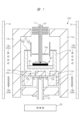
- FIG. 1 is a diagram showing a configuration of a single crystal manufacturing apparatus according to an embodiment.
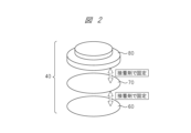
- FIG. 2 is a diagram showing a configuration of a seed crystal unit.
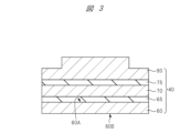
- FIG. 2 is a cross-sectional view showing a seed crystal unit.
- FIG. 1 is a diagram showing the configuration of a single crystal manufacturing apparatus 100 according to the present embodiment.
- the single crystal manufacturing apparatus 100 has a container 10.
- the internal space of this container 10 is filled with, for example, argon gas.
- An insulating member 13c is provided inside the container 10, and a pedestal 11 that can rotate horizontally is disposed inside the insulating member 13c.
- the container 10 is made of, for example, an iron-based material such as SUS.
- a structure for filling argon gas for example, a structure can be adopted in which a quartz tube is passed between the insulating member 13c and the coil 14a and between the insulating member 13c and the coil 14b, and the upper and lower ends of the quartz tube are sealed with flanges to fill the argon gas.
- crucible 12 is placed on pedestal 11.
- This crucible 12 is made of, for example, graphite, and contains a high-temperature solution 20 containing silicon (Si) inside.
- crucible 12 has a main body portion capable of containing solution 20 containing carbon and silicon, and a heat transfer portion 12a protruding from the bottom of the main body portion.
- the heat transfer portion 12a also functions as a "foot,” so it can be said that the heat transfer portion 12a also has the secondary function of stably standing the crucible 12 upright.
- the heat transfer portion 12a is configured to be in contact with the pedestal 11 on which the crucible 12 can be placed.
- the pedestal 11 includes a first region R1 in contact with the heat transfer portion 12a, a second region R2 surrounded by the first region R1, and a third region R3 surrounding the first region R1, and a heat insulating member 13a is provided so as to be in contact with the second region R2, and a heat insulating member 13b is provided so as to be in contact with the third region R3.
- the pedestal 11 is connected to a crucible holding shaft 18 that holds the pedestal 11.
- This crucible holding shaft 18 is configured to be movable in the vertical direction and to be able to rotate either clockwise or counterclockwise. This allows the pedestal 11 attached to the crucible holding shaft 18 and the crucible 12 placed on the pedestal 11 to be moved in the vertical direction and rotated horizontally by the crucible holding shaft 18.
- the crucible holding shaft 18 has a hollow structure inside, allowing a thermocouple or radiation thermometer to be inserted to measure temperature.
- the single crystal manufacturing apparatus 100 has heating units 25a and 25b.
- the heating unit 25a is configured to heat the crucible 12 by an induction heating phenomenon caused by passing a high-frequency current through the coil 14a provided in a position opposite the side of the crucible 12.
- the heating unit 25a is also shown in FIG. 1 in addition to the coil 14a.
- the heating unit 25b is configured to heat the pedestal 11 by an induction heating phenomenon caused by passing a high-frequency current through the coil 14b provided in a position opposite the pedestal 11 that supports the crucible 12. Then, the crucible 12 is heated by thermal conduction from the heated pedestal 11. In detail, heat is transferred from the pedestal 11 heated by the heating unit 25b to the heat transfer unit 12a, and then heat is transferred from the heat transfer unit 12a to the crucible 12 (main body) to heat the crucible 12. In this way, the heating unit 25b is configured to indirectly heat the crucible 12 through the pedestal 11 by an induction heating phenomenon caused by passing a high-frequency current through the coil 14b provided at a position opposite the pedestal 11 supporting the crucible 12.
- the coil 14b functions as the heating unit 25b that heats the crucible 12, and therefore the heating unit 25b is also shown in FIG. 1 in addition to the coil 14b.
- the coil 14b and the coil 14a are configured to allow cooling water to flow inside.
- the single crystal manufacturing apparatus 100 is configured so that not only does the heating section 25a heat the crucible 12 itself, but the crucible 12 is also heated by thermal conduction from the pedestal 11 heated by the heating section 25b, and it can be said that the heat transfer section 12a of the crucible 12 has the function of thermally conducting the heat from the pedestal 11 heated by the heating section 25b to the main body section.
- the thickness of the pedestal 11 is made thicker so that the portion facing the coil 14b is larger.
- This pedestal 11 can be integrated with the crucible 12, but considering the need to replace the crucible 12 every time a silicon carbide single crystal is manufactured and the high manufacturing costs of the integrated product, it is preferable to configure the pedestal 11 and the crucible 12 as separate bodies.
- the heat transfer portion 12a of the crucible 12 may simply be placed on the pedestal 11, or the pedestal 11 can be configured so that the heat transfer portion 12a can be fitted into the pedestal 11.
- heating units 25a and 25b are controlled by a control unit 50. That is, the single crystal manufacturing apparatus 100 has a control unit 50 that controls the power supplied to heating unit 25a and the power supplied to heating unit 25b.
- the power supply that supplies power to heating unit 25a and the power supply that supplies power to heating unit 25b are separate power supplies, and the control unit 50 is configured to be able to control heating unit 25a and heating unit 25b, which have different power supplies.
- the control unit 50 is configured to be able to alternate between a first operation of adjusting the power supplied to the heating unit 25a and the power supplied to the heating unit 25b so that the temperature of the solution 20 in contact with the side of the crucible 12 is higher than the temperature of the solution 20 in contact with the bottom of the crucible 12, and a second operation of adjusting the power supplied to the heating unit 25a and the power supplied to the heating unit 25b so that the temperature of the solution 20 in contact with the bottom of the crucible 12 is higher than the temperature of the solution 20 in contact with the side of the crucible 12.
- a crucible lid 15 is attached to the crucible 12, and this crucible lid 15 has a cylindrical member 15a and a connecting member 15b that connects to the cylindrical member 15a.
- This connecting member 15b has the function of fixing and supporting the cylindrical member 15a, and is configured to be able to come into contact with the crucible 12, for example.
- the single crystal manufacturing apparatus 100 is provided with a crystal holding shaft 16 that can move in the vertical direction.
- This crystal holding shaft 16 like the crucible holding shaft 18, may also be configured to be rotatable clockwise or counterclockwise.
- the crystal holding shaft 16 and the crucible holding shaft 18 may or may not have a rotation mechanism.
- a seed crystal unit 40 is attached to the tip of the crystal holding shaft 16.
- the crystal holding shaft 16 also has a fin structure 16a attached so as to intersect with the extension direction of the crystal holding shaft 16. Furthermore, the inside of the crystal holding shaft 16 has a hollow structure, and a thermocouple 17 is inserted into the crystal holding shaft 16 to measure the temperature near the seed crystal unit 40. Instead of inserting the thermocouple 17, the temperature near the seed crystal unit 40 can also be measured by placing a radiation thermometer with a measuring diameter smaller than the inner diameter of the crystal holding shaft 16 at the upper end of the crystal holding shaft 16.
- the control unit 50 of the single crystal manufacturing apparatus 100 is also configured to control the crystal holding shaft 16 having the fin structure 16a to move in the vertical direction. Specifically, the control unit 50 is configured to control the crystal holding shaft 16 so that the crystal holding shaft 16 having the fin structure 16a moves in the vertical direction through the inside of the cylindrical member 15a.
- the control unit 50 is configured to move the crystal holding shaft 16, to which the seed crystal unit 40 is attached at the tip, in the downward direction, so that the lower surface of the seed crystal unit 40 comes into contact with the surface of the solution 20 contained in the crucible 12, and to move the crystal holding shaft 16 in the upward direction after the lower surface of the seed crystal unit 40 comes into contact with the surface of the solution 20, so that a single crystal made of silicon carbide can be grown on the lower surface of the seed crystal unit 40.
- the seed crystal unit 40 may be brought into contact with the solution 20, but it is particularly preferable that the seed crystal unit 40 come into contact with the surface of the solution 20.
- the configuration in which a single crystal made of silicon carbide can be grown on the underside of the seed crystal unit 40 by moving the crystal holding shaft 16 upward is one example.
- the single crystal made of silicon carbide can be grown on the underside of the seed crystal unit 40 while the crystal holding shaft 16 is stopped (maintained), or the single crystal made of silicon carbide can be grown on the underside of the seed crystal unit 40 by moving the crystal holding shaft 16 downward.
- This configuration takes into consideration, for example, that the surface of the solution 20 may drop due to evaporation of the solution 20. In other words, if the surface of the solution 20 recedes due to evaporation of the solution 20, the single crystal can be reliably grown on the seed crystal unit 40 by growing the single crystal while moving the crystal holding shaft 16 downward.
- the single crystal manufacturing apparatus 100 is configured as described above.
- the heating section 25b for heating the pedestal 11 is an example that utilizes the induction heating phenomenon caused by passing a high-frequency current through the coil 14b.
- the heating section 25b for heating the pedestal 11 is not limited to this and may be composed of, for example, a resistance heater provided below the pedestal 11.
- the heating section 25b is made of a resistance heater, it is necessary to provide a "hole" in the insulating material in order to route the pair of wires used to energize the resistance heater.
- the crucible 12 itself is configured to rotate, it is necessary to provide a circumferential opening in the insulating material in order to route the pair of wires. As a result, it may become difficult to ensure the high temperature retention characteristics of the crucible 12. Therefore, from the viewpoint of increasing the insulating effect of the insulating material and simplifying the configuration of the single crystal manufacturing apparatus 100, it is desirable that the heating section 25b that heats the pedestal 11 be made of an induction heater that utilizes the induction heating phenomenon as shown in FIG. 1.
- the control unit 50 lowers the crystal holding shaft 16, which has a seed crystal unit 40 attached to its tip.
- the seed crystal unit 40 attached to the crystal holding shaft 16 passes through the inside of the cylindrical member 15a of the crucible lid 15, and then comes into contact with the surface of the solution 20 containing carbon and silicon contained in the crucible 12.
- the fin structure 16a attached to the crystal holding shaft 16 is positioned opposite the inner wall of the cylindrical member 15a.
- the control unit 50 slowly raises the crystal holding shaft 16. This causes a silicon carbide single crystal to grow on the underside of the seed crystal unit 40 being pulled up. At this time, the fin structure 16a attached to the crystal holding shaft 16 moves while maintaining its position facing the inner wall of the cylindrical member 15a. If crystal growth is to continue, the pulling operation of the crystal holding shaft 16 continues. On the other hand, if crystal growth is to end, the control unit 50 further raises the crystal holding shaft 16 to separate the silicon carbide single crystal from the solution 20. This ends the growth of the silicon carbide single crystal. At this time, the fin structure 16a attached to the crystal holding shaft 16 remains positioned facing the inner wall of the cylindrical member 15a.
- silicon carbide single crystals can be manufactured. Although it has been described that crystal growth is terminated by further pulling up the crystal holding shaft 16 to separate the silicon carbide single crystal from the solution 20, this is not limiting, and for example, instead of pulling up the crystal holding shaft 16, the crucible holding shaft 18 can be pulled down to separate the silicon carbide single crystal from the solution 20 and terminate the crystal growth.
- FIG. 2 is a diagram showing the configuration of the seed crystal unit 40.
- the seed crystal unit 40 is composed of a seed crystal substrate 60 formed from a silicon carbide single crystal, a carbon sheet 70 made of carbon, and a carbon jig 80 made of carbon.
- the seed crystal substrate 60 and the carbon sheet 70 are bonded together with an adhesive.
- the carbon sheet 70 and the carbon jig 80 are bonded together with an adhesive.
- the seed crystal substrate 60 is, for example, a wafer formed from a silicon carbide single crystal.
- This seed crystal substrate 60 has a main surface (upper surface) that is adhered to the carbon sheet 70, and a lower surface (rear surface) located opposite the main surface.
- the lower surface of the seed crystal substrate 60 is brought into contact with the solution 20 shown in FIG. 1. This allows a silicon carbide single crystal to grow on the lower surface of the seed crystal substrate 60.
- the carbon sheet 70 is a sheet-like member made of carbon, and is arranged so as to be interposed between the seed crystal substrate 60 and the carbon jig 80. This carbon sheet 70 is provided to relieve the stress acting between the seed crystal substrate 60 and the carbon jig 80. In other words, the carbon sheet 70 functions as a stress relief sheet that relieves the stress caused by the difference in the thermal expansion coefficient between the seed crystal substrate 60 and the carbon jig 80.
- the carbon jig 80 has, for example, a screw hole (not shown) and is configured so that, for example, the crystal holding shaft 16 shown in FIG. 1 can be inserted therein. In other words, the carbon jig 80 has the function of fixing the seed crystal unit 40 to the tip of the crystal holding shaft 16.
- Figure 3 is a cross-sectional view showing the seed crystal unit 40.
- the seed crystal substrate 60 has a main surface 60A and a bottom surface 60B.
- the bottom surface 60B is the surface that comes into contact with the solution 20 shown in FIG. 1.
- an adhesive layer 65 is formed on the main surface 60A.
- the seed crystal substrate 60 has the main surface 60A and the adhesive layer 65 formed on the main surface 60A.
- a carbon sheet 70 is arranged so as to be adhered to the main surface 60A of the seed crystal substrate 60 via the adhesive layer 65.
- a carbon jig 80 is arranged so as to be adhered to the carbon sheet 70 via the adhesive layer 75.
- each of the adhesive layers 65 and 75 is made of, for example, an adhesive containing phenol.
- the adhesive containing phenol is, for example, a photoresist.
- Photoresist is usually used for patterning using photolithography technology, but in this embodiment, photoresist is used as an adhesive. This is because photoresist has the following advantages: (1) it has low viscosity and is therefore easy to apply, and (2) a method for controlling the thickness of the applied layer using a spin coater has been established, allowing for precise control of the thickness of the adhesive layer.
- the seed crystal unit 40 is constructed as described above.
- the present inventors have newly discovered that roughening the main surface 60A of the seed crystal substrate 60 by performing a surface roughening treatment makes the seed crystal substrate 60 more susceptible to cracking. Specifically, when the roughness of the main surface 60A is made rough, the difference in roughness between the main surface 60A and the roughness (e.g., about 1 nm) of the lower surface 60B, which has not been subjected to a surface roughening treatment, becomes large.
- the inventors speculate that the Twyman effect generates stress in the seed crystal substrate 60, and that the heating performed when bonding the seed crystal substrate 60 and the carbon sheet 70 via the adhesive layer 65 causes cracks in the seed crystal substrate 60.
- the main surface 60A of the seed crystal substrate 60 constituting the seed crystal unit 40 is roughened from the viewpoint of ensuring adhesive strength.
- this common knowledge increases the possibility of cracks occurring in the seed crystal substrate 60.
- roughening the main surface 60A is useful from the viewpoint of ensuring adhesive strength, there is room for improvement in that the side effect of cracks occurring in the seed crystal substrate 60 becomes apparent. Therefore, ingenuity is required to achieve both improvement in adhesive strength between the main surface of the seed crystal substrate and the adhesive layer and suppression of cracks in the seed crystal substrate.
- the basic idea in this embodiment is to reduce the roughness of the main surface 60A of the seed crystal substrate 60 while increasing the thickness of the adhesive layer 65.
- the roughness of the main surface 60A is reduced, and the difference in roughness with the lower surface 60B is reduced, so that the occurrence of the Twyman effect, which causes stress, can be suppressed. Therefore, according to the basic idea, the occurrence of cracks in the seed crystal substrate 60 can be suppressed.
- the surface area of the main surface 60A is reduced, so that the adhesive strength between the main surface 60A and the adhesive layer 65 may be reduced.
- the basic idea is to increase the thickness of the adhesive layer 65.
- the decrease in the adhesive strength between the main surface 60A and the adhesive layer 65 can be suppressed.
- the roughness of the main surface 60A is reduced to suppress the occurrence of cracks in the seed crystal substrate 60, and the decrease in the adhesive strength between the main surface 60A and the adhesive layer 65, which becomes apparent when the roughness of the main surface 60A is reduced, is prevented by increasing the thickness of the adhesive layer 65. From the above, according to the basic concept, it is possible to improve the adhesive strength between the main surface 60A of the seed crystal substrate 60 and the adhesive layer 65 while suppressing cracking of the seed crystal substrate 60.
- roughness refers to "Ra.”
- Ra is a height-direction parameter known as “arithmetic mean roughness.”
- “Ra” is obtained by extracting a portion of the roughness curve measured with a roughness meter over a reference length and expressing the unevenness of that section as an average value. Because “Ra” uses an average value, it is less susceptible to the influence of a single protruding scratch, and has the advantage of providing stable results when evaluating surface roughness.
- the manufacturing method of the seed crystal unit 40 For example, we will explain an example in which a seed crystal substrate 60 with a diameter of 150 mm is used.
- the main surface 60A of the seed crystal substrate 60 coated with photoresist is attached to the carbon sheet 70, and heated to 200°C or higher on a hot plate. This allows the seed crystal substrate 60 and the carbon sheet 70 to be bonded together via the adhesive layer 65.
- the carbon sheet 70 and the carbon jig 80 are bonded together via the adhesive layer 75. After that, they are heated and sintered to 1000°C or higher in an inert atmosphere. This allows the seed crystal unit 40 to be manufactured.
- the distinctive feature of this embodiment is that the roughness of the main surface 60A of the seed crystal substrate 60 is 10 nm or less, and the thickness of the adhesive layer 65 that bonds the seed crystal substrate 60 and the carbon sheet 70 is 3 ⁇ m or more and 30 ⁇ m or less.
- the roughness of the main surface 60A of the seed crystal substrate 60 is 10 nm or less, and because the roughness of the main surface 60A is small, the difference in roughness with the underside 60B is small, which makes it possible to suppress the occurrence of the Twyman effect, which causes stress. Therefore, according to the characteristic features of the embodied embodiment, the occurrence of cracks in the seed crystal substrate 60 can be suppressed.
- the roughness Ra (arithmetic mean roughness) was calculated by evaluating the center of the seed crystal substrate 60 using a Bruker optical interference microscope (Contour GT-K) with a 50x lens and the VXI method (Vertical Scan Interferometry: high-resolution vertical scanning interferometry).
- the thickness of the adhesive layer 65 that bonds the seed crystal substrate 60 and the carbon sheet 70 is 3 ⁇ m or more and 30 ⁇ m or less, so even if the roughness of the main surface 60A is small, the thick adhesive layer 65 can suppress a decrease in the adhesive strength between the main surface 60A and the adhesive layer 65.
- the characteristic features of the embodied embodiment are that the roughness of the main surface 60A of the seed crystal substrate 60 is 10 nm or less, and that the thickness of the adhesive layer 65 that bonds the seed crystal substrate 60 and the carbon sheet 70 is 3 ⁇ m or more and 30 ⁇ m or less.
- the numerical range stipulated by this characteristic feature is not met, cracks in the seed crystal substrate 60 and peeling of the carbon sheet 70 from the seed crystal substrate 60 may occur. An example of this will be described.
- 5 ml of photoresist was dropped onto the center of the seed crystal substrate, and the substrate was rotated under the conditions of (1) 600 rpm x 20 seconds, and then (2) 1500 rpm x 20 seconds to spread the photoresist.
- the carbon sheet peeled off from the seed crystal substrate. This is thought to be because the thickness of the photoresist was about 2 ⁇ m, which is smaller than 3 ⁇ m, and the adhesive strength between the main surface of the seed crystal substrate and the adhesive layer was reduced, resulting in the carbon sheet peeling off.
- the numerical ranges stipulated by the characteristic points in the embodied embodiment are exceeded, there is a risk that the seed crystal substrate may crack or the carbon sheet may peel off from the seed crystal substrate. Therefore, in order to simultaneously improve the adhesive strength between the seed crystal substrate and the carbon sheet and prevent cracking of the seed crystal substrate, it is useful to realize the characteristic points in the embodied embodiment.
Landscapes
- Chemical & Material Sciences (AREA)
- Engineering & Computer Science (AREA)
- Crystallography & Structural Chemistry (AREA)
- Materials Engineering (AREA)
- Metallurgy (AREA)
- Organic Chemistry (AREA)
- Inorganic Chemistry (AREA)
- Crystals, And After-Treatments Of Crystals (AREA)
Abstract
種結晶基板の主面と接着層との接着強度の向上と、種結晶基板の割れの抑制とを両立する。種結晶基板60(接着層付き種結晶基板)は、主面60Aと、主面60A上に形成された接着層65と、を備える。ここで、接着層65は、フェノールを含む接着剤から構成され、接着層65の厚さは、3μm以上であり、主面60Aの粗度は、10nm以下である。
Description
本発明は、接着層付き種結晶基板および種結晶ユニットに関し、例えば、溶液成長法によって単結晶を成長させるための接着層付き種結晶基板および種結晶ユニットに適用して有効な技術に関する。
特開2015-30659号公報(特許文献1)には、放電加工によって炭化珪素からなる種結晶基板の接着面を粗くする(粗度:Ra>500nm)ことにより、接着強度を向上させる技術が記載されている。
例えば、溶液成長法によって単結晶を成長させるために、成長の核を提供する種結晶ユニットが使用される。この種結晶ユニットは、例えば、主面を有する種結晶基板と、接着層を介して種結晶基板の主面と接着するシート状部材と、シート状部材と接着する治具とを備える。このとき、種結晶基板とシート状部材とは接着層によって接着されるが、種結晶基板の主面と接着層との接着強度を向上させるために、種結晶基板の主面の粗度を粗くする(Ra>30nm)ことが行われている。
ところが、接着層を介して種結晶基板とシート状部材とを接着する際、加熱することが行われるが、本発明者は、この加熱工程に起因して、種結晶基板が割れてしまうことを新規な知見として獲得した。したがって、本発明者が見出した新規な知見に基づくと、種結晶基板の主面と接着層との接着強度を向上する必要がある一方で、種結晶基板の割れを抑制することが望まれている。すなわち、種結晶基板の主面と接着層との接着強度の向上と、種結晶基板の割れの抑制とを両立することが望まれている。
一実施の形態における接着層付き種結晶基板は、主面と、主面上に形成された接着層と、を備える。ここで、接着層は、フェノールを含む接着剤から構成され、接着層の厚さは、3μm以上であり、主面の粗度は、10nm以下である。
一実施の形態における種結晶ユニットは、主面を有する種結晶基板と、接着層を介して種結晶基板の主面と接着するシート状部材と、シート状部材と接着する治具とを備える。ここで、接着層は、フェノールを含む接着剤から構成され、接着層の厚さは、3μm以上であり、主面の粗度は、10nm以下である。
一実施の形態によれば、種結晶基板の主面と接着層との接着強度の向上と、種結晶基板の割れの抑制とを両立できる。
実施の形態を説明するための全図において、同一の部材には原則として同一の符号を付し、その繰り返しの説明は省略する。なお、図面をわかりやすくするために平面図であってもハッチングを付す場合がある。
<単結晶製造装置の構成>
図1は、本実施の形態における単結晶製造装置100の構成を示す図である。
図1は、本実施の形態における単結晶製造装置100の構成を示す図である。
図1において、単結晶製造装置100は、容器10を有している。この容器10の内部空間には、例えば、アルゴンガスが充填されている。また、容器10の内部には、断熱部材13cが設けられており、断熱部材13cで囲まれた内側に水平方向に回転可能な台座11が配置されている。容器10は、例えば、SUSなどの鉄系材料から構成される。
なお、アルゴンガスの充填構造としては、例えば、断熱部材13cとコイル14aとの間および断熱部材13cとコイル14bの間に石英管を通し、石英管の上下端をフランジで密閉することにより、アルゴンガスを充填する構造を採用することもできる。
次に、台座11上には、坩堝12が配置されている。この坩堝12は、例えば、黒鉛(グラファイト)から構成されており、内部に珪素(Si)を含む高温の溶液20が収容されている。具体的に、坩堝12は、炭素と珪素とを含む溶液20を収容可能な本体部と、本体部の底部から突出する伝熱部12aとを備える。
このように構成されている坩堝12は、伝熱部12aが「足部」としても機能することから、伝熱部12aは、坩堝12を安定して直立させる副次的な機能も有しているといえる。伝熱部12aは、坩堝12を配置可能な台座11と接触するように構成されている。例えば、図1に示すように、台座11は、伝熱部12aと接触する第1領域R1と、第1領域R1に囲まれる第2領域R2と、第1領域R1を囲む第3領域R3とを含んでおり、第2領域R2と接触するように断熱部材13aが設けられているとともに、第3領域R3と接触するように断熱部材13bが設けられている。
台座11は、台座11を保持する坩堝保持軸18と接続されている。この坩堝保持軸18は、上下方向に移動可能に構成されているとともに、時計回り、あるいは、反時計回りのいずれにも回転することができるように構成されている。これにより、坩堝保持軸18に取り付けられた台座11および台座11上に配置される坩堝12は、坩堝保持軸18によって上下方向に移動させることができるとともに水平方向に回転させることができる。なお、坩堝保持軸18は、内部が中空構造となっており、熱電対や放射温度計を挿入して温度測定が可能なように構成されている。
そして、単結晶製造装置100の容器10の外周部には、高周波電流が流れるコイルが設けられており、コイルを流れる高周波電流に基づく誘導加熱によって坩堝12は加熱されるようになっている。具体的に、単結晶製造装置100は、加熱部25aと加熱部25bを有している。加熱部25aは、坩堝12の側面と対向する位置に設けられたコイル14aに高周波電流を流すことによって生じる誘導加熱現象で坩堝12を加熱するように構成されている。つまり、コイル14aは、坩堝12を加熱する加熱部25aとして機能することから、図1では、コイル14aに対して、加熱部25aも併記している。一方、加熱部25bは、坩堝12を支持する台座11と対向する位置に設けられたコイル14bに高周波電流を流すことによって生じる誘導加熱現象で台座11を加熱するように構成されている。そして、加熱された台座11からの熱伝導によって坩堝12が加熱されることになる。詳細には、加熱部25bによって加熱された台座11から伝熱部12aに熱が伝わり、続いて、伝熱部12aから坩堝12(本体部)に熱が伝わって坩堝12が加熱される。このように、加熱部25bは、坩堝12を支持する台座11と対向する位置に設けられたコイル14bに高周波電流を流すことによって生じる誘導加熱現象で台座11を介して間接的に坩堝12を加熱するように構成されている。このことから、コイル14bは、坩堝12を加熱する加熱部25bとして機能することから、図1では、コイル14bに対して、加熱部25bも併記している。なお、図1では、図示されていないが、コイル14bおよびコイル14aは、内部に冷却水を流すことができるように構成されている。
このように、単結晶製造装置100では、加熱部25aで坩堝12自体を加熱するだけでなく、加熱部25bで加熱された台座11からの熱伝導によっても坩堝12が加熱されるように構成されており、坩堝12の伝熱部12aは、加熱部25bによって加熱された台座11からの熱を本体部に熱伝導させる機能を有しているといえる。
ここで、加熱部25bによって、台座11を加熱しやすくするため、台座11の厚さは、コイル14bと対向する部分が大きくなるように厚くなっている。この台座11は、坩堝12と一体化することも可能であるが、坩堝12は炭化珪素単結晶を製造するたびに取り替える必要性および一体物の製造コストが高いことを考慮すると、台座11と坩堝12は別体として構成することが望ましい。台座11と坩堝12を別体として構成する場合、坩堝12の伝熱部12aを台座11上に配置するだけの構成でもよいし、伝熱部12aを台座11に嵌め込むことが可能なように台座11を構成することもできる。
これらの加熱部25aおよび加熱部25bは、制御部50によって制御される。すなわち、単結晶製造装置100は、加熱部25aに供給する電力と加熱部25bに供給する電力を制御する制御部50を有する。例えば、加熱部25aに電力を供給する電源と、加熱部25bに電力を供給する電源とは、別電源となっており、制御部50は、電源の異なる加熱部25aと加熱部25bとをそれぞれ制御できるように構成されている。
制御部50は、坩堝12の側面と接する溶液20の温度を坩堝12の底面と接する溶液20の温度よりも高くするように、加熱部25aに供給する電力と加熱部25bに供給する電力とを調整する第1動作と、坩堝12の底面と接する溶液20の温度を坩堝12の側面と接する溶液20の温度よりも高くするように、加熱部25aに供給する電力と加熱部25bに供給する電力とを調整する第2動作とを交互に切り替えることができるように構成されている。
加熱部25aおよび加熱部25bによって加熱される坩堝12に収容されている溶液20は、高温となっており、坩堝12を構成する黒鉛(C)が溶け出すことから、溶液20は、炭素と珪素を含むことになる。坩堝12には、坩堝用蓋15が取り付けられており、この坩堝用蓋15は、筒状部材15aと、筒状部材15aと接続される接続部材15bを有している。この接続部材15bは、筒状部材15aを固定して支持する機能を有し、例えば、坩堝12と接触可能に構成されている。
次に、単結晶製造装置100には、上下方向に移動可能な結晶保持軸16が設けられている。この結晶保持軸16も坩堝保持軸18と同様に、時計回り、あるいは、反時計回りに回転できるように構成されていてもよい。つまり、結晶保持軸16および坩堝保持軸18において、回転機構の有無は任意である。
結晶保持軸16の先端部には、種結晶ユニット40が取り付けられている。また、結晶保持軸16には、結晶保持軸16の延在方向と交差するように取り付けられたフィン構造体16aを有している。さらに、結晶保持軸16の内部は中空構造となっており、結晶保持軸16の内部に種結晶ユニット40近傍の温度を測定するための熱電対17が挿入されている。種結晶ユニット40近傍の温度測定は、熱電対17を挿入する代わりに、結晶保持軸16の上端に結晶保持軸16の内径よりも小さな測定径を有する放射温度計を配置することによっても可能である。
そして、単結晶製造装置100の制御部50は、フィン構造体16aを有する結晶保持軸16を上下方向に移動させるように制御するようにも構成されている。具体的に、この制御部50は、フィン構造体16aを有する結晶保持軸16が筒状部材15aの内部を通って上下方向に移動するように結晶保持軸16を制御するように構成されている。制御部50は、先端部に種結晶ユニット40が取り付けられた結晶保持軸16を下方向に移動させることにより、種結晶ユニット40の下面を坩堝12に収容された溶液20の表面に接触させるように構成されているとともに、種結晶ユニット40の下面を溶液20の表面に接触させた後、結晶保持軸16を上方向に移動させることにより、種結晶ユニット40の下面に炭化珪素からなる単結晶を成長させることができるように構成されている。なお、種結晶ユニット40は、溶液20に接触させればよいが、特に、溶液20の表面に接触させることが望ましい。
なお、結晶保持軸16を上方向に移動させることにより、種結晶ユニット40の下面に炭化珪素からなる単結晶を成長させることができるように構成することは一例であり、例えば、結晶保持軸16を停止(維持)した状態で、種結晶ユニット40の下面に炭化珪素からなる単結晶を成長させるように構成してもよいし、結晶保持軸16を下方向に移動させることにより、種結晶ユニット40の下面に炭化珪素からなる単結晶を成長させるように構成することもできる。この構成は、例えば、溶液20の蒸発によって、溶液20の表面が下がる場合もあることを考慮したものである。すなわち、溶液20の蒸発によって、溶液20の表面が後退する場合、結晶保持軸16を下方向に移動させながら、単結晶を成長させることにより、確実に種結晶ユニット40に単結晶を成長させることができる。
以上のようにして、単結晶製造装置100が構成されている。
<変形例>
図1に示す単結晶製造装置100では、台座11を加熱する加熱部25bは、コイル14bに高周波電流を流すことによって生じる誘導加熱現象を利用する例を示しているが、台座11を加熱する加熱部25bは、これに限らず、例えば、台座11の下方に設けられた抵抗加熱ヒータから構成されていてもよい。
図1に示す単結晶製造装置100では、台座11を加熱する加熱部25bは、コイル14bに高周波電流を流すことによって生じる誘導加熱現象を利用する例を示しているが、台座11を加熱する加熱部25bは、これに限らず、例えば、台座11の下方に設けられた抵抗加熱ヒータから構成されていてもよい。
ただし、加熱部25bを抵抗加熱ヒータから構成する場合、抵抗加熱ヒータを通電するために使用される一対の配線を引き回すため、断熱材に「孔」を設ける必要がある。特に、坩堝12自体を回転させる構成の場合、一対の配線を引き回すため、断熱材には、円周状の開口部を設ける必要がある。この結果、坩堝12の高温保持特性を確保することが難しくなるおそれがある。したがって、断熱材の断熱効果を高める観点および単結晶製造装置100の構成を簡略化する観点からは、台座11を加熱する加熱部25bは、図1に示すような誘導加熱現象を利用した誘導加熱ヒータから構成することが望ましい。
<単結晶製造装置の動作(単結晶製造方法)>
続いて、単結晶製造装置100の動作を説明する。
続いて、単結晶製造装置100の動作を説明する。
まず、制御部50は、先端部に種結晶ユニット40が取り付けられた結晶保持軸16を下降させる。これにより、結晶保持軸16に取り付けられた種結晶ユニット40は、坩堝用蓋15に備わる筒状部材15aの内部を通過した後、坩堝12に収容された炭素と珪素とを含む溶液20の表面に接触する。このとき、結晶保持軸16に取り付けられたフィン構造体16aは、筒状部材15aの内壁と対向する位置に配置される。
次に、制御部50は、結晶保持軸16をゆっくり上昇させる。これにより、引き上げられる種結晶ユニット40の下面に炭化珪素単結晶が成長する。このとき、結晶保持軸16に取り付けられたフィン構造体16aは、筒状部材15aの内壁との対向を維持しながら移動する。その後、結晶成長を継続する場合、結晶保持軸16の引き上げ動作を継続する。一方、結晶成長を終了する場合、制御部50は、結晶保持軸16をさらに引き上げて、炭化珪素単結晶と溶液20とを隔離させる。これにより、炭化珪素単結晶の成長を終了させる。このとき、結晶保持軸16に取り付けられたフィン構造体16aは、筒状部材15aの内壁と対向する位置に配置されている状態が維持されている。
以上のようにして、単結晶製造装置100を動作させることにより、炭化珪素単結晶を製造することができる。なお、結晶保持軸16をさらに引き上げて、炭化珪素単結晶と溶液20とを隔離させることによって、結晶成長を終了すると記載したが、これに限らず、例えば、結晶保持軸16を引き上げる代わりに、坩堝保持軸18を引き下げることにより、炭化珪素単結晶と溶液20とを隔離させて、結晶成長を終了することもできる。
<種結晶ユニットの構成>
続いて、種結晶ユニット40の構成について説明する。
続いて、種結晶ユニット40の構成について説明する。
図2は、種結晶ユニット40の構成を示す図である。図2に示すように、種結晶ユニット40は、炭化珪素単結晶から形成される種結晶基板60、カーボンからなるカーボンシート70およびカーボンからなるカーボン治具80から構成されている。そして、種結晶基板60とカーボンシート70とは、接着剤で接着されている。同様に、カーボンシート70とカーボン治具80とは、接着剤で接着されている。
種結晶基板60は、例えば、炭化珪素単結晶から形成されるウェハである。この種結晶基板60は、カーボンシート70と接着する主面(上面)と、主面とは反対側に位置する下面(裏面)を有している。種結晶基板60の下面は、図1に示す溶液20に接触させる。これにより、種結晶基板60の下面に炭化珪素単結晶を成長させることができる。
カーボンシート70は、カーボンからなるシート状部材であり、種結晶基板60とカーボン治具80との間に介在するように配置される。このカーボンシート70は、種結晶基板60とカーボン治具80との間に働く応力を緩和するために設けられている。つまり、カーボンシート70は、種結晶基板60とカーボン治具80との熱膨張率の相違に起因して発生する応力を緩和する応力緩和シートとして機能する。
カーボン治具80は、例えば、ネジ穴(図示せず)を有しており、例えば、図1に示す結晶保持軸16を挿入可能に構成されている。すなわち、カーボン治具80は、種結晶ユニット40を結晶保持軸16の先端部に固定する機能を有している。
図3は、種結晶ユニット40を示す断面図である。
図3において、種結晶基板60は、主面60Aと下面60Bを有している。下面60Bは、図1に示す溶液20に接触させる面である。一方、主面60Aには、接着層65が形成されている。このように、種結晶基板60は、主面60Aと、主面60A上に形成された接着層65と、を備える。そして、接着層65を介して種結晶基板60の主面60Aと接着するようにカーボンシート70が配置されている。さらに、接着層75を介してカーボンシート70と接着するようにカーボン治具80が配置されている。
ここで、接着層65および接着層75のそれぞれは、例えば、フェノールを含む接着剤から構成されている。フェノールを含む接着剤は、例えば、フォトレジストである。
フォトレジストは、通常、フォトリソグラフィ技術を使用したパターニングに使用されるが、本実施の形態では、フォトレジストを接着剤として使用している。なぜなら、フォトレジストは、(1)粘度が低いため塗布が容易である点、(2)スピンコータを利用した塗布厚の制御法が確立されているため、接着層の厚さを正確に制御できる点に代表される利点を有しているからである。
以上のようにして、種結晶ユニット40が構成されている。
<改善の検討>
上述した種結晶ユニット40において、接着層65を介した種結晶基板60とカーボンシート70との接着強度を確保する必要がある。このことから、種結晶基板60の主面60Aの粗度を粗くすることが行われている。なぜなら、主面60Aの粗度を粗くすることにより、主面60Aの表面積が大きくなる結果、種結晶基板60の主面60Aと接着層65との接着強度を向上できるからである。すなわち、いままでの技術では、例えば、背景技術に記載した特許文献1のように、接着強度を確保する観点から、種結晶ユニット40を構成する種結晶基板60の主面60Aを粗くすることが一般的である。
上述した種結晶ユニット40において、接着層65を介した種結晶基板60とカーボンシート70との接着強度を確保する必要がある。このことから、種結晶基板60の主面60Aの粗度を粗くすることが行われている。なぜなら、主面60Aの粗度を粗くすることにより、主面60Aの表面積が大きくなる結果、種結晶基板60の主面60Aと接着層65との接着強度を向上できるからである。すなわち、いままでの技術では、例えば、背景技術に記載した特許文献1のように、接着強度を確保する観点から、種結晶ユニット40を構成する種結晶基板60の主面60Aを粗くすることが一般的である。
この点に関し、本発明者は、粗面化処理を施すことによって種結晶基板60の主面60Aを粗くすると、種結晶基板60に割れが発生しやすくなることを新規に見出している。具体的には、主面60Aの粗度を粗くすると、粗面化処理をしていない下面60Bの粗度(例えば、1nm程度)との差が大きくなる。
この結果、トワイマン効果によって、種結晶基板60に応力が生じ、接着層65を介して種結晶基板60とカーボンシート70とを接着する際に実施される加熱によって種結晶基板60に割れが発生すると本発明者は推測している。すなわち、接着強度を確保する観点から、種結晶ユニット40を構成する種結晶基板60の主面60Aを粗くするということが当業者における常識である。ところが、この常識では、種結晶基板60に割れが発生する可能性が高まることを本発明者は新規に見出している。つまり、主面60Aを粗くするということは、接着強度を確保する観点から有用である一方、種結晶基板60に割れが発生するという副作用が顕在化する点において、改善の余地が存在する。したがって、種結晶基板の主面と接着層との接着強度の向上と、種結晶基板の割れの抑制とを両立するためには工夫が必要とされる。
そこで、本実施の形態では、種結晶基板の主面と接着層との接着強度の向上と、種結晶基板の割れの抑制とを両立するための工夫を施している。以下では、この工夫を施した本実施の形態における技術的思想について説明する。
<実施の形態における基本思想>
本実施の形態における基本思想は、種結晶基板60の主面60Aの粗度を小さくする一方、接着層65の厚さを厚くする思想である。これにより、主面60Aの粗度が小さくなるため、下面60Bとの粗度の差が小さくなる結果、応力の起因となるトワイマン効果の発生を抑制できる。このため、基本思想によれば、種結晶基板60の割れの発生を抑制できる。ただし、この場合、主面60Aの表面積が小さくなることから、主面60Aと接着層65との接着強度が低下するおそれがある。この点に関し、基本思想では、接着層65の厚さを厚くする。これにより、主面60Aと接着層65との接着強度の低下を抑制できる。つまり、基本思想では、まず、主面60Aの粗度を小さくすることによって、種結晶基板60の割れの発生を抑制するとともに、主面60Aの粗度を小さくすることによって顕在化する主面60Aと接着層65との接着強度の低下を接着層65の厚さを厚くすることによって防止している。以上のことから、基本思想によれば、種結晶基板60の主面60Aと接着層65との接着強度の向上と、種結晶基板60の割れの抑制を両立できる。
本実施の形態における基本思想は、種結晶基板60の主面60Aの粗度を小さくする一方、接着層65の厚さを厚くする思想である。これにより、主面60Aの粗度が小さくなるため、下面60Bとの粗度の差が小さくなる結果、応力の起因となるトワイマン効果の発生を抑制できる。このため、基本思想によれば、種結晶基板60の割れの発生を抑制できる。ただし、この場合、主面60Aの表面積が小さくなることから、主面60Aと接着層65との接着強度が低下するおそれがある。この点に関し、基本思想では、接着層65の厚さを厚くする。これにより、主面60Aと接着層65との接着強度の低下を抑制できる。つまり、基本思想では、まず、主面60Aの粗度を小さくすることによって、種結晶基板60の割れの発生を抑制するとともに、主面60Aの粗度を小さくすることによって顕在化する主面60Aと接着層65との接着強度の低下を接着層65の厚さを厚くすることによって防止している。以上のことから、基本思想によれば、種結晶基板60の主面60Aと接着層65との接着強度の向上と、種結晶基板60の割れの抑制を両立できる。
なお、本明細書でいう粗度とは、「Ra」を意味する。「Ra」とは、「算術平均粗さ」と呼ばれる高さ方向のパラメータである。「Ra」は、粗さ計で測定した粗さ曲線の一部を基準長さで抜き出し、その区間の凹凸状態を平均値で表すことにより取得される。「Ra」は、平均値を用いるため、1つの突出したキズの影響を受けにくく、表面粗さを評価する上で安定した結果が得られるという利点を有している。
<具現化態様>
以下では、上述した基本思想を具現化した具現化態様について説明する。
以下では、上述した基本思想を具現化した具現化態様について説明する。
まず、種結晶ユニット40の製造方法について簡単に説明する。例えば、φ=150mmの種結晶基板60を使用する例について説明する。
種結晶基板60の中央部に5mlのフォトレジストを滴下する。そして、スピンコータで(1)600rpm×20秒の条件で回転させた後、(2)1500rpm×20秒の条件で回転させることにより、フォトレジストを塗り広げる。この結果、種結晶基板60の主面60A上にフォトレジストからなる接着層65が形成される。このとき、接着層65の厚さは、3μm~4μmとなる。
続いて、フォトレジストを塗布した種結晶基板60の主面60Aとカーボンシート70とを貼り合わせて、ホットプレート上で200℃以上に加熱する。これにより、接着層65を介して種結晶基板60とカーボンシート70とを接着できる。
次に、接着層75を介してカーボンシート70とカーボン治具80とを貼り合わせる。その後、不活性雰囲気中で1000℃以上に加熱・焼成する。これにより、種結晶ユニット40を製造することができる。
ここで、具現化態様における特徴点は、種結晶基板60の主面60Aの粗度が10nm以下であるとともに、種結晶基板60とカーボンシート70とを接着する接着層65の厚さが3μm以上30μm以下である点にある。
これにより、まず、種結晶基板60の主面60Aの粗度が10nm以下であり、主面60Aの粗度が小さいことから、下面60Bとの粗度の差が小さくなる結果、応力の起因となるトワイマン効果の発生を抑制できる。したがって、具現化態様における特徴点によれば、種結晶基板60の割れの発生を抑制できる。
ここで、粗度Ra(算術平均粗さ)は、「Bruker」の光干渉型顕微鏡(「ContourGT-K」)を使用し、50倍レンズ、VXI方式(Vertical Scan Interferometry:高分解能垂直走査型干渉法)で種結晶基板60の中心を評価して算出している。
そして、具現化態様における特徴点によれば、種結晶基板60とカーボンシート70とを接着する接着層65の厚さが3μm以上30μm以下であることから、主面60Aの粗度が小さくても、厚さの厚い接着層65によって、主面60Aと接着層65との接着強度の低下を抑制できる。このように、特徴点によれば、種結晶基板60の主面60Aと接着層65との接着強度の向上と、種結晶基板60の割れの抑制とを両立できる。この結果、特徴点によれば、種結晶基板60とカーボンシート70との接着強度の向上と、種結晶基板60の割れの抑制とを両立できる。
上述したように、具現化態様における特徴点は、種結晶基板60の主面60Aの粗度が10nm以下であるとともに、種結晶基板60とカーボンシート70とを接着する接着層65の厚さが3μm以上30μm以下である点であるが、以下では、この特徴点で規定する数値範囲から外れると、種結晶基板60の割れや、種結晶基板60からのカーボンシート70の剥離が発生することがある。この例について説明する。
まず、粗度が大きい結果、種結晶基板が割れた例について説明する。
例えば、銅定盤を使用し、粒径5s(3μm~8μm)のダイヤ砥粒で種結晶基板の主面を加工して、主面の粗度をRa=33.5nmとした。その後、5mlのフォトレジストを種結晶基板の中央に滴下し、(1)600rpm×20秒の条件で回転させた後、(2)1500rpm×20秒の条件で回転させることにより、フォトレジストを塗り広げた。そして、種結晶基板とカーボンシートとを貼り合わせてプリベークしたところ、種結晶基板にクラック(割れ)が発生した。これは、主面の粗度がRa=10nmよりも大きいRa=33.5nmであるため、種結晶基板に割れが発生したと考えられる。
続いて、フォトレジストの厚さが薄い結果、種結晶基板からカーボンシートが剥がれた例について説明する。例えば、Pla-Pad定盤を使用し、粒径5s(3μm~8μm)のダイヤ砥粒で種結晶基板の主面を加工して、主面の粗度をRa=5.9nmとした。その後、5mlのフォトレジストを種結晶基板の中央に滴下し、(1)600rpm×20秒の条件で回転させた後、(2)3000rpm×20秒の条件で回転させることにより、フォトレジストを塗り広げた。このとき、フォトレジストの厚さは、3μm未満(2μm程度)である。そして、種結晶基板とカーボンシートとを貼り合わせてプリベークしたところ、種結晶基板からカーボンシートが剥離した。これは、フォトレジストの厚さが3μmよりも小さい2μm程度であるため、種結晶基板の主面と接着層との接着強度が低下した結果、カーボンシートの剥離が発生したと考えられる。
以上のことから、具現化態様における特徴点で規定する数値範囲から外れると、種結晶基板の割れや、種結晶基板からのカーボンシートの剥離が発生するおそれがある。したがって、種結晶基板とカーボンシートとの接着強度の向上と、種結晶基板の割れの抑制とを両立するためには、具現化態様における特徴点を実現することが有用である。
以上、本発明者によってなされた発明をその実施の形態に基づき具体的に説明したが、本発明は前記実施の形態に限定されるものではなく、その要旨を逸脱しない範囲で種々変更可能であることは言うまでもない。
10 容器
11 台座
12 坩堝
12a 伝熱部
13a 断熱部材
13b 断熱部材
13c 断熱部材
14a コイル
14b コイル
15 坩堝用蓋
15a 筒状部材
15b 接続部材
16 結晶保持軸
16a フィン構造体
17 熱電対
18 坩堝保持軸
20 溶液
25a 加熱部
25b 加熱部
40 種結晶ユニット
50 制御部
60 種結晶基板
60A 主面
60B 下面
65 接着層
70 カーボンシート
75 接着層
80 カーボン治具
100 単結晶製造装置
R1 第1領域
R2 第2領域
R3 第3領域
11 台座
12 坩堝
12a 伝熱部
13a 断熱部材
13b 断熱部材
13c 断熱部材
14a コイル
14b コイル
15 坩堝用蓋
15a 筒状部材
15b 接続部材
16 結晶保持軸
16a フィン構造体
17 熱電対
18 坩堝保持軸
20 溶液
25a 加熱部
25b 加熱部
40 種結晶ユニット
50 制御部
60 種結晶基板
60A 主面
60B 下面
65 接着層
70 カーボンシート
75 接着層
80 カーボン治具
100 単結晶製造装置
R1 第1領域
R2 第2領域
R3 第3領域
Claims (8)
- 主面と、
前記主面上に形成された接着層と、
を備える、接着層付き種結晶基板であって、
前記接着層は、フェノールを含む接着剤から構成され、
前記接着層の厚さは、3μm以上であり、
前記主面の粗度は、10nm以下である、接着層付き種結晶基板。 - 請求項1に記載の接着層付き種結晶基板において、
前記接着層は、フォトレジストから構成されている。 - 請求項1に記載の接着層付き種結晶基板において、
前記接着層の厚さは、30μm以下である。 - 請求項1に記載の接着層付き種結晶基板において、
前記接着層付き種結晶基板は、炭化珪素から構成されている。 - 主面を有する種結晶基板と、
接着層を介して前記種結晶基板の前記主面と接着するシート状部材と、
前記シート状部材と接着する治具と、
を備える、種結晶ユニットであって、
前記接着層は、フェノールを含む接着剤から構成され、
前記接着層の厚さは、3μm以上であり、
前記主面の粗度は、10nm以下である、種結晶ユニット。 - 請求項5に記載の種結晶ユニットにおいて、
前記接着層は、フォトレジストから構成されている。 - 請求項5に記載の種結晶ユニットにおいて、
前記接着層の厚さは、30μm以下である。 - 請求項5に記載の種結晶ユニットにおいて、
前記種結晶基板は、炭化珪素から構成され、
前記シート状部材は、カーボンシートであり、
前記治具は、カーボン治具である。
Applications Claiming Priority (2)
| Application Number | Priority Date | Filing Date | Title |
|---|---|---|---|
| JP2023-165984 | 2023-09-27 | ||
| JP2023165984A JP2025056481A (ja) | 2023-09-27 | 2023-09-27 | 接着層付き種結晶基板および種結晶ユニット |
Publications (1)
| Publication Number | Publication Date |
|---|---|
| WO2025069751A1 true WO2025069751A1 (ja) | 2025-04-03 |
Family
ID=95203765
Family Applications (1)
| Application Number | Title | Priority Date | Filing Date |
|---|---|---|---|
| PCT/JP2024/028911 Ceased WO2025069751A1 (ja) | 2023-09-27 | 2024-08-13 | 接着層付き種結晶基板および種結晶ユニット |
Country Status (2)
| Country | Link |
|---|---|
| JP (1) | JP2025056481A (ja) |
| WO (1) | WO2025069751A1 (ja) |
Citations (7)
| Publication number | Priority date | Publication date | Assignee | Title |
|---|---|---|---|---|
| JP2005247681A (ja) * | 2004-02-04 | 2005-09-15 | Matsushita Electric Ind Co Ltd | 種結晶の固定方法及びその固定方法を用いた単結晶の製造方法 |
| JP2006143511A (ja) * | 2004-11-18 | 2006-06-08 | Matsushita Electric Ind Co Ltd | 種結晶固定部及び種結晶固定方法 |
| WO2009116581A1 (ja) * | 2008-03-21 | 2009-09-24 | 株式会社ブリヂストン | 炭化ケイ素単結晶の製造方法 |
| JP2010280547A (ja) * | 2009-06-05 | 2010-12-16 | Bridgestone Corp | 炭化珪素単結晶の製造方法 |
| WO2011010394A1 (ja) * | 2009-07-21 | 2011-01-27 | トヨタ自動車株式会社 | 溶液法による単結晶成長用種結晶軸 |
| JP2016056059A (ja) * | 2014-09-09 | 2016-04-21 | トヨタ自動車株式会社 | SiC単結晶製造装置 |
| JP2021066649A (ja) * | 2019-10-22 | 2021-04-30 | エスケイシー・カンパニー・リミテッドSkc Co., Ltd. | 種結晶接着層、それを適用した積層体の製造方法及びウエハの製造方法 |
-
2023
- 2023-09-27 JP JP2023165984A patent/JP2025056481A/ja active Pending
-
2024
- 2024-08-13 WO PCT/JP2024/028911 patent/WO2025069751A1/ja not_active Ceased
Patent Citations (7)
| Publication number | Priority date | Publication date | Assignee | Title |
|---|---|---|---|---|
| JP2005247681A (ja) * | 2004-02-04 | 2005-09-15 | Matsushita Electric Ind Co Ltd | 種結晶の固定方法及びその固定方法を用いた単結晶の製造方法 |
| JP2006143511A (ja) * | 2004-11-18 | 2006-06-08 | Matsushita Electric Ind Co Ltd | 種結晶固定部及び種結晶固定方法 |
| WO2009116581A1 (ja) * | 2008-03-21 | 2009-09-24 | 株式会社ブリヂストン | 炭化ケイ素単結晶の製造方法 |
| JP2010280547A (ja) * | 2009-06-05 | 2010-12-16 | Bridgestone Corp | 炭化珪素単結晶の製造方法 |
| WO2011010394A1 (ja) * | 2009-07-21 | 2011-01-27 | トヨタ自動車株式会社 | 溶液法による単結晶成長用種結晶軸 |
| JP2016056059A (ja) * | 2014-09-09 | 2016-04-21 | トヨタ自動車株式会社 | SiC単結晶製造装置 |
| JP2021066649A (ja) * | 2019-10-22 | 2021-04-30 | エスケイシー・カンパニー・リミテッドSkc Co., Ltd. | 種結晶接着層、それを適用した積層体の製造方法及びウエハの製造方法 |
Also Published As
| Publication number | Publication date |
|---|---|
| JP2025056481A (ja) | 2025-04-08 |
Similar Documents
| Publication | Publication Date | Title |
|---|---|---|
| JP7290687B2 (ja) | 静電チャック及びその製造方法と基板処理装置 | |
| JP6404355B2 (ja) | 温度プロファイル制御装置を有する加熱基板支持体 | |
| JP6172301B2 (ja) | 静電チャック装置 | |
| TWI470691B (zh) | 靜電式夾持裝置 | |
| TWI788497B (zh) | 靜電吸盤裝置 | |
| KR100495987B1 (ko) | 가열장치 | |
| TW201133702A (en) | Electrostatic chuck device | |
| JPH1064983A (ja) | ウエハステージ | |
| JP4328009B2 (ja) | 加熱装置 | |
| CN113774476A (zh) | 一种电阻加热的物理气相传输法单晶生长炉 | |
| CN111501096A (zh) | 一种晶体制备装置 | |
| US20140158042A1 (en) | Apparatus for fabricating ingot | |
| JP2016058748A (ja) | 静電チャック装置 | |
| JP5098873B2 (ja) | 気相成長装置用のサセプタ及び気相成長装置 | |
| TWI916544B (zh) | SiC單晶成長裝置及SiC結晶成長方法 | |
| JP6236158B2 (ja) | インゴット成長装置 | |
| CN105980614B (zh) | 单晶生长装置 | |
| JP2025056481A (ja) | 接着層付き種結晶基板および種結晶ユニット | |
| JP5281480B2 (ja) | 静電チャック | |
| JP2011081932A (ja) | 加熱ヒータおよびそれを搭載した装置 | |
| JP4035136B2 (ja) | 種結晶の固定方法及びその固定方法を用いた単結晶の製造方法 | |
| CN111733387A (zh) | 高温蒸发源及其冷却装置 | |
| JP2000133698A (ja) | 半導体基板保持装置 | |
| TWI770953B (zh) | 長晶爐 | |
| TWI640053B (zh) | 基板支撐台及其製造方法 |
Legal Events
| Date | Code | Title | Description |
|---|---|---|---|
| 121 | Ep: the epo has been informed by wipo that ep was designated in this application |
Ref document number: 24871553 Country of ref document: EP Kind code of ref document: A1 |
|
| NENP | Non-entry into the national phase |
Ref country code: DE |