WO2025057736A1 - 基板処理方法、接合装置、及び接合システム - Google Patents
基板処理方法、接合装置、及び接合システム Download PDFInfo
- Publication number
- WO2025057736A1 WO2025057736A1 PCT/JP2024/030683 JP2024030683W WO2025057736A1 WO 2025057736 A1 WO2025057736 A1 WO 2025057736A1 JP 2024030683 W JP2024030683 W JP 2024030683W WO 2025057736 A1 WO2025057736 A1 WO 2025057736A1
- Authority
- WO
- WIPO (PCT)
- Prior art keywords
- substrate
- carrier
- die
- bonding
- attached
- Prior art date
- Legal status (The legal status is an assumption and is not a legal conclusion. Google has not performed a legal analysis and makes no representation as to the accuracy of the status listed.)
- Ceased
Links
Images




Classifications
-
- H—ELECTRICITY
- H10—SEMICONDUCTOR DEVICES; ELECTRIC SOLID-STATE DEVICES NOT OTHERWISE PROVIDED FOR
- H10P—GENERIC PROCESSES OR APPARATUS FOR THE MANUFACTURE OR TREATMENT OF DEVICES COVERED BY CLASS H10
- H10P95/00—Generic processes or apparatus for manufacture or treatments not covered by the other groups of this subclass
Definitions
- the chip mounting system described in Patent Document 1 includes a chip supply device, a bonding device, a surface treatment device, an input/output section, and a transport section (paragraph [0225] of Patent Document 1).
- the chip supply device supplies multiple chips individually.
- the chips are attached to tape that covers the opening of the frame, and are pushed upward one by one and turned upside down one by one (paragraph [0251] of Patent Document 1).
- the bonding device attaches the chips supplied from the chip supply device onto a substrate.
- One aspect of the present disclosure provides a technique for standardizing the time it takes to bond each of multiple dies.
- a substrate processing method includes preparing a substrate having a first base substrate and a plurality of first devices formed on the first base substrate; preparing a die-attached carrier having a carrier substrate, a carrier having a resin film formed on the carrier substrate, and a plurality of dies attached to the carrier substrate via the resin film; and bonding the substrate and the die-attached carrier to collectively bond the plurality of dies to the substrate.
- Each of the plurality of dies has a second base substrate and a second device formed on the second base substrate. The plurality of first devices and the plurality of second devices are electrically connected collectively.
- the time required to bond each of multiple dies can be made uniform.
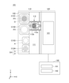
- FIG. 1 is a plan view showing a transfer system according to an embodiment.
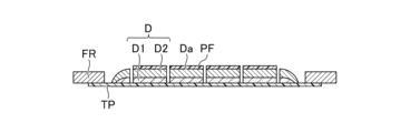
- FIG. 2 is a cross-sectional view of one example of a die attached to a tape covering an opening in a frame.
- FIG. 3 is a cross-sectional view showing an example of a carrier.
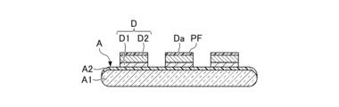
- FIG. 4 is a cross-sectional view showing an example of a die mounted on a carrier.
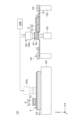
- FIG. 5 is a cross-sectional view showing a transfer device according to an embodiment.
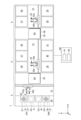
- FIG. 6 is a top view of a bonding system according to one embodiment.
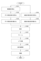
- FIG. 7 is a flow chart illustrating a bonding method according to one embodiment.
- FIG. 8 is a cross-sectional view showing an example of a substrate.
- FIG. 1 is a plan view showing a transfer system according to an embodiment.
- FIG. 2 is a cross-sectional view of one example of a die attached to a tape covering an opening in a frame.
- FIG. 3 is a cross-sectional view showing an example
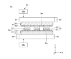
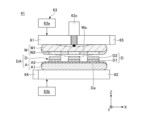
- FIG. 9 is a cross-sectional view showing a state at the start of welding of the welding apparatus according to one embodiment.
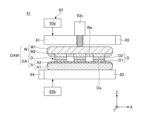
- FIG. 10 is a cross-sectional view showing a state of the joining apparatus shown in FIG. 9 upon completion of joining.
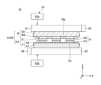
- FIG. 11 is a cross-sectional view showing a state at the start of welding of the welding apparatus according to the modified example.
- FIG. 12 is a cross-sectional view showing a state of the welding apparatus shown in FIG. 11 upon completion of welding.
- FIG. 13 is a cross-sectional view showing an example of an irradiation device.
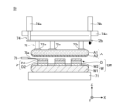
- FIG. 14 is a cross-sectional view showing a state of the separation device at the start of separation.
- 15 is a cross-sectional view showing a state during the peeling process of the peeling apparatus shown in FIG.
- FIG. 16 is a cross-sectional view showing a state when the separation device shown in FIG. 14 has completed separation.
- the X-axis, Y-axis, and Z-axis directions are perpendicular to each other.
- the X-axis and Y-axis directions are horizontal directions, and the Z-axis direction is vertical.
- the X-axis direction includes the positive X-axis direction and the negative X-axis direction that is the opposite direction to the positive X-axis direction.
- the Y-axis direction includes the positive Y-axis direction and the negative Y-axis direction that is the opposite direction to the positive Y-axis direction.
- the Z-axis direction includes the positive Z-axis direction and the negative Z-axis direction that is the opposite direction to the positive Z-axis direction.
- a transfer system 101 will be described with reference mainly to Figures 1 to 5.
- the transfer system 101 transfers the die D from the tape TP covering the opening of the frame FR to the carrier A.
- the carrier A has higher durability than the tape TP. Therefore, as shown in Figures 9 to 10 (or Figures 11 to 12), the joining surface Da of the die D can be appropriately treated before joining the die D to the substrate W, and the die D can be appropriately joined to the substrate W.
- the die D has a second base substrate D1 and a second device D2 formed on the second base substrate D1.
- the second base substrate D1 is, for example, a silicon wafer or a compound semiconductor wafer.
- the second device D2 includes a semiconductor element, a circuit, a terminal, or the like.
- the die D has a second device D2 electrically connected to a first device W2 of the substrate W on a bonding surface Da with the substrate W.
- One second device D2 is electrically connected to one first device W2, but multiple second devices D2 may be electrically connected.
- the multiple dies D are obtained, for example, by dicing the second base substrate D1 etc. while the second base substrate D1 etc. is adhered to the tape TP.
- the bonding surface Da of the die D is protected by a protective film PF before dicing.
- the protective film PF is disposed on the opposite side of the die D from the tape TP. The protective film PF is removed before bonding the die D to the substrate W.
- the carrier A has a carrier substrate A1 and a resin film A2, and the die D is attached to the opposite side of the carrier substrate A1 with the resin film A2 as a reference.
- the resin film A2 has, for example, adhesiveness.
- the die D may be adsorbed to the resin film A2 by pressing the die D against the resin film A2.
- the resin film A2 can be deformed so as to remove gas from between the die D and the resin film A2, and the die D can be vacuum-adsorbed to the resin film A2.
- the carrier A does not electrostatically adsorb the die D. Therefore, a device for applying a voltage between the carrier A and the die D is not required, and the structure of the transfer device 121 can be simplified.
- the carrier substrate A1 may be conductive or insulating.
- the carrier substrate A1 is made of, for example, glass, silicon, aluminum, an aluminum alloy, stainless steel, or titanium.
- the carrier substrate A1 may have a through hole penetrating the carrier substrate A1 in the thickness direction.
- the die D can be peeled off from the carrier A by supplying gas to the through hole or by inserting a pin (not shown) into the through hole.
- the number and arrangement of the through holes are not particularly limited. One or more through holes may be formed for each die D.
- the resin film A2 is preferably made of a flexible material, specifically a material with an elastic modulus of 2 GPa or less, more preferably 0.5 GPa or less. From the viewpoint of durability when modifying the bonding surface Da, the resin film A2 is preferably made of, for example, polyimide or EVA (ethylene-vinyl acetate copolymer). The thickness of the resin film A2 is, for example, 10 ⁇ m. Note that, although the resin film A2 is a single layer in this embodiment, it may be made of multiple layers. For example, the resin film A2 may have a polyolefin layer and an acrylic adhesive layer.
- the transfer system 101 includes a loading/unloading station 110, a processing station 120, and a control circuit 190.
- the loading/unloading station 110 and the processing station 120 are arranged in this order from the negative side of the X-axis to the positive side of the X-axis.
- the loading/unloading station 110 includes a mounting table 102.
- Cassettes C101 to C104 are mounted on the mounting table 102.
- Cassette C101 contains a frame FR on which a die D is attached via a tape TP.
- Cassette C102 contains a frame FR from which the die has been peeled off.
- Cassette C103 contains a carrier A before the die D is attached.
- Cassette C104 contains a carrier A on which a die D is attached (i.e., a die-attached carrier DA).
- the loading/unloading station 110 includes a transport area 111 and a transport device 112.
- the transport area 111 is adjacent to the mounting table 102.
- the transport area 111 extends in the Y-axis direction.
- the transport device 112 includes a carrier transport arm 112a and a frame transport arm 112b.
- the carrier transport arm 112a holds and transports a carrier A in the transport area 111.
- the carrier A to be transported may be one before the die D is attached, or one after the die D has been attached (i.e., a die-attached carrier DA).
- the frame transport arm 112b holds and transports a frame FR in the transport area 111.
- the frame FR to be transported may be one with the die D attached, or one from which the die D has been peeled off.
- the transport device 112 has a drive unit (not shown) that moves or rotates the carrier transport arm 112a and the frame transport arm 112b.
- the carrier transport arm 112a and the frame transport arm 112b can move horizontally (in both the X-axis and Y-axis directions) and vertically (in the Z-axis direction), and can rotate around a vertical axis.
- the carrier transport arm 112a and the frame transport arm 112b may be mounted on the same Y-axis slider and moved simultaneously in the Y-axis direction as shown in FIG. 1, or may be mounted on different Y-axis sliders and moved independently in the Y-axis direction.
- the carrier transport arm 112a and the frame transport arm 112b are positioned at different heights.
- the control circuit 190 is, for example, a computer, and includes an arithmetic unit 191 such as a CPU (Central Processing Unit), and a storage unit 192 such as a memory.
- the storage unit 192 stores programs that control various processes executed in the transfer system 101.
- the control circuit 190 controls the operation of the transfer system 101 by having the arithmetic unit 191 execute the programs stored in the storage unit 192.
- a lower control circuit that controls the operation of each device constituting the transfer system 101 may be provided, and a higher-level control circuit that controls multiple lower-level control circuits may be provided.
- the control circuit 190 may be configured with the lower control circuit and the higher-level control circuit.
- the control circuit 190 includes electronic circuits such as a CPU, a Field Programmable Gate Array (FPGA) or an Application Specific Integrated Circuit (ASIC), and executes the various control operations described in this specification by executing instruction codes stored in memory or by being a circuit designed for a specific purpose.
- FPGA Field Programmable Gate Array
- ASIC Application Specific Integrated Circuit
- the frame transport arm 112b removes the frame FR on which the die D is attached from the cassette C101 and transports it to the transfer device 121.
- the carrier transport arm 112a removes the carrier A from the cassette C103 and transports it to the transfer device 121.
- the transfer device 121 transfers the die D from the tape TP covering the opening of the frame FR to the carrier A.
- the carrier transport arm 112a removes the carrier A on which the die D is attached (i.e., the die-attached carrier DA) from the transfer device 121 and transports it to the cassette C104.
- the frame transport arm 112b removes the frame FR from which the die D has been peeled off from the transfer device 121 and transports it to the cassette C102.
- the transfer device 121 includes a frame holding section 122, a pressing section 123, a carrier holding section 124, and a conveying section 125.
- the frame holding section 122 holds the frame FR.
- the frame FR holds the die D, for example, with the joining surface Da of the die D facing upward.
- the pressing unit 123 locally presses the die D through the tape TP and locally deforms the tape TP.
- the dies D can be pushed up individually, and when the transport unit 125 picks up the dies D, rubbing between the dies D can be suppressed.
- the pressing unit 123 and the frame holding unit 122 can move relative to each other, and the position at which the die D is pushed up can be changed.
- the carrier holding unit 124 holds the carrier A.
- the carrier A holds the die D, for example, with the joining surface Da of the die D facing upward.
- the transport unit 125 transports the die D with the joining surface Da of the die D facing upward.
- the transport unit 125 does not turn the die D upside down.
- the transport unit 125 presses the die D against the resin film A2 to adsorb it.
- the transport unit 125 has a suction head 125a and a moving mechanism 125b.
- the suction head 125a suctions the die D.
- the suction head 125a suctions the die D while facing the joining surface Da of the die D.
- the joining surface Da of the die D is covered with a protective film PF, and the suction head 125a suctions the die D via the protective film PF.
- the suction head 125a comes into contact with the protective film PF, but does not come into contact with the die D. This prevents contamination of the joining surface Da of the die D.
- the moving mechanism 125b moves the suction head 125a between a peeling position and an attachment position.
- the peeling position is a position where the suction head 125a peels the die D from the tape TP.
- the attachment position is a position where the suction head 125a attaches the die D to the carrier A.
- An alignment mark (not shown) may be provided on the carrier A.
- the control circuit 190 may correct the attachment position based on an image of the alignment mark.
- the bonding system 1 manufactures a laminated substrate DAW by bonding a die-attached carrier DA and a substrate W.
- the laminated substrate DAW has a die-attached carrier DA and a substrate W.
- the bonding system 1 then manufactures a die-attached substrate DW by removing the carrier A from the laminated substrate DAW as shown in Figure 16.
- the die-attached substrate DW includes a substrate W and a plurality of dies D bonded to the substrate W.
- the substrate W has a first base substrate W1 and a plurality of first devices W2 formed on the first base substrate W1.
- the first base substrate W1 is, for example, a silicon wafer or a compound semiconductor wafer.
- the first devices W2 include semiconductor elements, circuits, terminals, etc.
- the substrate W has a plurality of first devices W2 on a bonding surface Wa with the die D.
- the first devices W2 of the substrate W and the second devices D2 of the die D are electrically connected.
- a second die may be prepared separately from the die D.
- the second die has a third device on its bonding surface with the substrate W, which is electrically connected to the first device W2 of the substrate W.
- the third device has a different function, i.e., a different electrical circuit, from the second device D2.
- the second device D2 and the third device may be electrically connected to one first device W2.
- One third device is electrically connected to one first device W2, but multiple third devices may also be electrically connected.
- the bonding system 1 includes a loading/unloading station 2, a first processing station 3, a second processing station 5, and a control circuit 90.
- the loading/unloading station 2, the first processing station 3, and the second processing station 5 are arranged in this order from the negative side of the X-axis to the positive side of the X-axis.
- the loading/unloading station 2 includes a mounting table 20.
- Cassettes C1 to C4 are mounted on the mounting table 20.
- Cassette C1 contains a carrier A with a die D attached (i.e., die-attached carrier DA).
- Cassette C2 contains a carrier A from which the die D has been peeled off.
- Cassette C3 contains a substrate W before the die-attached carrier DA is bonded.
- Cassette C4 contains a substrate W after the carrier A has been removed from the laminated substrate DAW (i.e., die-attached substrate DW).
- carrier A has the same diameter as substrate W.
- the transport arm that transports carrier A and the transport arm that transports substrate W can have the same model number (i.e., the same dimensions and shape), reducing costs.
- the first activation device 37 and the second activation device 39, or the first hydrophilization device 38 and the second hydrophilization device 40 can have the same model number, reducing costs. This also prevents the device from becoming too large.
- the loading/unloading station 2 includes a third transport area 21 and a third transport device 22.
- the third transport area 21 is adjacent to the mounting table 20.
- the third transport area 21 extends in the Y-axis direction.
- the third transport device 22 includes a third carrier transport arm 22a and a third substrate transport arm 22b.
- the third carrier transport arm 22a holds and transports a carrier A in the third transport area 21.
- the carrier A to be transported may be one to which a die D is attached (i.e., a die-attached carrier DA) or one to which a die D has been peeled off.
- the third substrate transport arm 22b holds and transports a substrate W in the third transport area 21.
- the substrate W to be transported may be one to which a die-attached carrier DA has not yet been joined or one to which a carrier A has been removed from a laminated substrate DAW (i.e., a die-attached substrate DW).
- the third transport device 22 has a drive unit (not shown) that moves or rotates the third carrier transport arm 22a and the third substrate transport arm 22b.
- the third carrier transport arm 22a and the third substrate transport arm 22b can move horizontally (in both the X-axis and Y-axis directions) and vertically (in the Z-axis direction), and can rotate around a vertical axis.
- the third carrier transport arm 22a and the third substrate transport arm 22b may be mounted on the same Y-axis slider and moved simultaneously in the Y-axis direction as shown in FIG. 6, or may be mounted on different Y-axis sliders and moved independently in the Y-axis direction.
- the third carrier transport arm 22a and the third substrate transport arm 22b are positioned at different heights.
- the first processing station 3 includes a first transfer area 31 and a first transfer device 32.
- the first transfer area 31 extends in the X-axis direction.
- the first transfer device 32 includes a first carrier transfer arm 32a and a first substrate transfer arm 32b.
- the first carrier transfer arm 32a holds and transfers a carrier A in the first transfer area 31.
- the carrier A to be transferred may be one to which a die D is attached (i.e., a die-attached carrier DA), one to which a die-attached carrier DA and a substrate W are joined (i.e., a laminated substrate DAW), or one from which a die D has been peeled off.
- the first substrate transfer arm 32b holds and transfers a substrate W in the first transfer area 31.
- the substrate W to be transferred may be one to which a die-attached carrier DA has not yet been joined, or one to which a carrier A has been removed from a laminated substrate DAW (i.e., a die-attach
- the first transport device 32 has a drive unit (not shown) that moves or rotates the first carrier transport arm 32a and the first substrate transport arm 32b.
- the first carrier transport arm 32a and the first substrate transport arm 32b can move horizontally (in both the X-axis and Y-axis directions) and vertically (in the Z-axis direction), and can rotate around a vertical axis.
- the first carrier transport arm 32a and the first substrate transport arm 32b may be mounted on the same X-axis slider and moved simultaneously in the X-axis direction as shown in FIG. 6, or may be mounted on different X-axis sliders and moved independently in the X-axis direction.
- the first carrier transport arm 32a and the first substrate transport arm 32b are positioned at different heights.
- the first processing station 3 includes a third transition device 34, a fourth transition device 35, a cleaning device 36, a first activation device 37, a first hydrophilization device 38, a second activation device 39, a second hydrophilization device 40, and a bonding device 41.
- the third transition device 34, the fourth transition device 35, the cleaning device 36, the first activation device 37, the first hydrophilization device 38, the second activation device 39, the second hydrophilization device 40, and the bonding device 41 are adjacent to the first transport area 31.
- the third transition device 34 is provided between the third transport area 21 and the first transport area 31, and temporarily stores the carrier A.
- the third transition device 34 relays the carrier A between the third carrier transport arm 22a and the first carrier transport arm 32a.
- the relaying carrier A may be one with a die D attached (i.e., a die-attached carrier DA) or one from which the die D has been peeled off.
- the fourth transition device 35 is provided between the third transfer area 21 and the first transfer area 31, and temporarily stores the substrate W.
- the fourth transition device 35 relays the substrate W between the third substrate transfer arm 22b and the first substrate transfer arm 32b.
- the substrate W to be relayed may be one before the die-attached carrier DA is joined, or one from which the carrier A has been removed from the laminated substrate DAW (i.e., a die-attached substrate DW).
- the cleaning device 36 removes the protective film PF from the die D while the die D is held by the carrier A.
- the protective film PF protects the bonding surface Da of the die D, for example, during dicing. If the protective film PF is water-soluble, the cleaning device 36 supplies pure water to the protective film PF. After removing the protective film PF from the die D, the cleaning device 36 may further clean the bonding surface Da of the die D. This can improve the quality of the processing of the bonding surface Da of the die D that is performed thereafter.
- the first activation device 37 activates the bonding surface Da of the die D while the die D is held by the carrier A.
- the first activation device 37 is, for example, a plasma processing device.
- oxygen gas which is a processing gas
- the bonding surface Da of the die D is activated by irradiating the oxygen ions onto the bonding surface Da of the die D.
- the processing gas is not limited to oxygen gas, and may be, for example, nitrogen gas, etc.
- the first hydrophilization device 38 hydrophilizes the bonding surface Da of the die D while the die D is held by the carrier A.
- the first hydrophilization device 38 supplies pure water (e.g., deionized water) onto the die D while rotating the carrier A held by the spin chuck.
- the pure water imparts OH groups to the bonding surface Da of the die D, which has been activated in advance.
- the die D and the substrate W can be bonded by utilizing hydrogen bonds between the OH groups.
- the second activation device 39 activates the bonding surface Wa of the substrate W.
- the second activation device 39 is, for example, a plasma processing device.
- oxygen gas which is a processing gas
- the bonding surface Wa of the substrate W is activated by irradiating the oxygen ions onto the bonding surface Wa of the substrate W.
- the processing gas is not limited to oxygen gas, and may be, for example, nitrogen gas, etc.
- the second hydrophilization device 40 hydrophilizes the bonding surface Wa of the substrate W.
- the second hydrophilization device 40 supplies pure water (e.g., deionized water) onto the substrate W while rotating the substrate W held by the spin chuck.
- the pure water imparts OH groups to the bonding surface Wa of the substrate W, which has been activated in advance.
- the die D and the substrate W can be bonded by utilizing hydrogen bonds between the OH groups.
- the bonding device 41 bonds a substrate W and a die-attached carrier DA together, thereby bonding multiple dies D to the substrate W at once.
- a plurality of first devices W2 and a plurality of second devices D2 are electrically connected together. Compared to bonding the dies D one by one to the substrate W, the time required to bond each of the multiple dies D can be made uniform, and variation in bonding quality can be reduced. Details of the bonding device 41 will be described later.
- the mounting position of the die D is adjusted for each die D by the transfer device 121, and the accuracy of the bonding position of the die D can be improved. Note that even if the die D is transported one by one from the tape TP to the carrier A in order to adjust the mounting position of the die D for each die D, the variation in bonding quality does not increase. This is because the carrier A is eventually separated from the die D.
- the second processing station 5 includes a second transfer area 51 and a second transfer device 52.
- the second transfer area 51 extends in the X-axis direction.
- the second transfer device 52 includes a second carrier transfer arm 52a and a second substrate transfer arm 52b.
- the second carrier transfer arm 52a holds and transfers a carrier A in the second transfer area 51.
- the carrier A to be transferred may be a substrate W bonded to a die-attached carrier DA (i.e., a laminated substrate DAW) or a substrate from which the die D has been peeled off.
- the second substrate transfer arm 52b holds and transfers a substrate W in the second transfer area 51.
- the substrate W to be transferred may be a substrate W bonded to a die-attached carrier DA (i.e., a laminated substrate DAW) or a substrate W from which the carrier A has been removed (i.e., a substrate DW with a die).
- a die-attached carrier DA i.e., a laminated substrate DAW
- a substrate W from which the carrier A has been removed i.e., a substrate DW with a die
- the second transport device 52 has a drive unit (not shown) that moves or rotates the second carrier transport arm 52a and the second substrate transport arm 52b.
- the second carrier transport arm 52a and the second substrate transport arm 52b can move horizontally (in both the X-axis and Y-axis directions) and vertically (in the Z-axis direction), and can rotate around a vertical axis.
- the second carrier transport arm 52a and the second substrate transport arm 52b may be mounted on the same X-axis slider and moved simultaneously in the X-axis direction as shown in FIG. 6, or may be mounted on different X-axis sliders and moved independently in the X-axis direction.
- the second carrier transport arm 52a and the second substrate transport arm 52b are positioned at different heights.
- the second processing station 5 includes a first transition device 54, a second transition device 55, an inversion device 56, an annealing device 57, an irradiation device 58, and a peeling device 59.
- the first transition device 54, the second transition device 55, the inversion device 56, the annealing device 57, the irradiation device 58, and the peeling device 59 are adjacent to the second transfer region 51. Equipped with.
- the first transition device 54 is provided between the first transport area 31 and the second transport area 51, and temporarily stores the carrier A.
- the first transition device 54 relays the carrier A between the first carrier transport arm 32a and the second carrier transport arm 52a.
- the relaying carrier A may be a carrier DA with a die attached and a substrate W joined together (i.e., a laminated substrate DAW), or a carrier from which the die D has been peeled off.
- the second transition device 55 is provided between the first transport area 31 and the second transport area 51, and temporarily stores the substrate W.
- the second transition device 55 relays the substrate W between the first substrate transport arm 32b and the second substrate transport arm 52b.
- the relayed substrate W may be a laminated substrate DAW from which the carrier A has been removed (i.e., a substrate DW with a die attached).
- the inversion device 56 inverts the laminated substrate DAW upside down, so that the carrier substrate A1 faces upward.
- the inversion (step S108) is preferably performed after annealing (step S107) and before UV irradiation (step S109). In other words, the inversion is preferably performed after improving the bonding strength between the die D and the substrate W and before reducing the adhesion of the resin film A2.
- the annealing device 57 anneals (heats) the laminated substrate DAW. Before the heat treatment, the die D and the substrate W are bonded by hydrogen bonds between OH groups. The heat treatment causes a dehydration condensation reaction, resulting in covalent bonds and improving the bonding strength between the die D and the substrate W.
- the irradiation device 58 irradiates the resin film A2 with ultraviolet light through the carrier substrate A1 as shown in FIG. 13.
- the carrier substrate A1 may be a glass substrate.
- the peeling device 59 peels off the multiple dies D and the carrier A, as shown in Figures 14 to 16.
- the carrier A can be removed from the laminated substrate DAW, and the carrier A and the substrate DW with the dies can be separated.
- the separated carrier A can be reused after replacing the resin film A2. Details of the peeling device 59 will be described later.
- the control circuit 90 is, for example, a computer, and includes an arithmetic unit 91 such as a CPU (Central Processing Unit), and a storage unit 92 such as a memory.
- the storage unit 92 stores programs that control various processes executed in the bonding system 1.
- the control circuit 90 controls the operation of the bonding system 1 by having the arithmetic unit 91 execute the programs stored in the storage unit 92.
- a lower control circuit that controls the operation of each device constituting the bonding system 1 may be provided, and a higher-level control circuit that controls multiple lower-level control circuits may be provided.
- the control circuit 90 may be composed of the lower-level control circuit and the higher-level control circuit.
- the control circuit 90 includes electronic circuits such as a CPU, FPGA (Field Programmable Gate Array) or ASIC (Application Specific Integrated Circuit), and executes the various control operations described in this specification by executing instruction codes stored in memory or by being a circuit designed for a specific purpose.
- electronic circuits such as a CPU, FPGA (Field Programmable Gate Array) or ASIC (Application Specific Integrated Circuit)
- FIG. 7 a joining method according to one embodiment will be described with reference to FIG. 7.
- the process of FIG. 7 is performed under the control of the control circuit 90.
- the third carrier transport arm 22a removes the die-attached carrier DA from the cassette C1 and transports it to the third transition device 34.
- the first carrier transport arm 32a removes the die-attached carrier DA from the third transition device 34 and transports it to the cleaning device 36.
- the cleaning device 36 removes the protective film PF from the die D while the die D is held by the carrier A (step S101).
- the first carrier transport arm 32a takes the carrier DA with the die from the cleaning device 36 and transports it to the first activation device 37.
- the first activation device 37 activates the bonding surface Da of the die D while the die D is held by the carrier A (step S102).
- the first carrier transport arm 32a removes the die-attached carrier DA from the first activation device 37 and transports it to the first hydrophilization device 38.
- the first hydrophilization device 38 hydrophilizes the bonding surface Da of the die D while the die D is held by the carrier A (step S103). After that, the first carrier transport arm 32a removes the die-attached carrier DA from the first hydrophilization device 38 and transports it to the bonding device 41.
- the third substrate transport arm 22b removes the substrate W from the cassette C3 and transports it to the fourth transition device 35. Then, the first substrate transport arm 32b removes the substrate W from the fourth transition device 35 and transports it to the second activation device 39.
- the second activation device 39 activates the bonding surface Wa of the substrate W (step S104).
- the first substrate transport arm 32b removes the substrate W from the second activation device 39 and transports it to the second hydrophilization device 40.
- the second hydrophilization device 40 hydrophilizes the bonding surface Wa of the substrate W (step S105).
- the first substrate transport arm 32b removes the substrate W from the second hydrophilization device 40 and transports it to the bonding device 41.
- the bonding device 41 bonds the substrate W and the die-attached carrier DA to bond multiple dies D to the substrate W at once (step S106). This results in a laminated substrate DAW.
- the first carrier transport arm 32a then removes the laminated substrate DAW from the bonding device 41 and transports it to the first transition device 54.
- the second carrier transport arm 52a then removes the laminated substrate DAW from the first transition device 54 and transports it to the annealing device 57.
- the annealing device 57 anneals (heats) the laminated substrate DAW (step S107).
- the heat treatment causes a dehydration condensation reaction, which creates covalent bonds and improves the bonding strength between the die D and the substrate W.
- the second carrier transport arm 52a then removes the laminated substrate DAW from the annealing device 57 and transports it to the inversion device 56.
- the inversion device 56 inverts the laminated substrate DAW upside down (step S108). This allows the carrier substrate A1 to face upward.
- the second substrate transport arm 52b removes the laminated substrate DAW from the inversion device 56 and transports it to the irradiation device 58.
- the irradiation device 58 irradiates the resin film A2 with ultraviolet light through the carrier substrate A1 (step S109).
- the adhesiveness of the resin film A2 can be reduced, making it easier to peel the carrier A and the die D.
- the second substrate transport arm 52b removes the laminated substrate DAW from the irradiation device 58 and transports it to the peeling device 59.
- the peeling device 59 peels off the multiple dies D and the carrier A (step S110).
- the carrier A can be removed from the laminated substrate DAW, and the carrier A and the substrate DW with the dies can be separated.
- the separated carrier A can be reused after replacing the resin film A2.
- the second substrate transport arm 52b removes the die-attached substrate DW from the peeling device 59 and transports it to the second transition device 55.
- the first substrate transport arm 32b removes the die-attached substrate DW from the second transition device 55 and transports it to the fourth transition device 35.
- the third substrate transport arm 22b removes the die-attached substrate DW from the fourth transition device 35 and stores it in cassette C4.
- the second carrier transport arm 52a then removes carrier A from the peeling device 59 and transports it to the first transition device 54.
- the first carrier transport arm 32a removes carrier A from the first transition device 54 and transports it to the third transition device 34.
- the third carrier transport arm 22a removes carrier A from the third transition device 34 and stores it in cassette C2.
- the bonding device 41 includes, for example, a first holding unit 61, a second holding unit 62, and a drive unit 63.
- the first holding unit 61 holds the substrate W from the opposite side to the second holding unit 62, with the bonding surface Wa of the substrate W facing the second holding unit 62.
- the second holding unit 62 holds the die-attached carrier DA from the opposite side to the first holding unit 61, with the bonding surface Da of the die D facing the first holding unit 61.
- the drive unit 63 moves the first holding unit 61 and the second holding unit 62 relatively to bond the substrate W and the die-attached carrier DA together, thereby bonding multiple dies D to the substrate W at once.
- the first holding part 61 is provided, for example, above the second holding part 62.
- the first holding part 61 holds the substrate W from above with the joining surface Wa of the substrate W facing downward.
- the first holding part 61 vacuum-adsorbs the substrate W.
- the second holding part 62 holds the die-attached carrier DA from below with the joining surface Da of the die D facing upward, for example.
- the second holding part 62 vacuum-adsorbs the die-attached carrier DA.
- the arrangement of the first holding part 61 and the second holding part 62 may be reversed, and the first holding part 61 may be provided below the second holding part 62.
- the first holding part 61 may hold the substrate W from below with the joining surface Wa of the substrate W facing upward.
- the second holding part 62 may hold the die-attached carrier DA from above with the joining surface Da of the die D facing downward.
- the bonding device 41 may include a first imaging unit 64 and a second imaging unit 65.
- the first imaging unit 64 images the bonding surface Wa of the substrate W held by the first holding unit 61.
- the first imaging unit 64 is provided in the second holding unit 62.
- the second imaging unit 65 images the bonding surface Da of the die D constituting the die-attached carrier DA held by the second holding unit 62.
- the second imaging unit 65 is provided in the first holding unit 61.
- the second imaging unit 65 may image the alignment mark of the carrier A instead of imaging the bonding surface Da of the die D.
- the control circuit 90 controls the drive unit 63 based on images captured by the first imaging unit 64 and the second imaging unit 65.
- the drive unit 63 has, for example, a first drive unit 63a and a second drive unit 63b.
- the first drive unit 63a rotates the first holding unit 61 around a vertical axis.
- the second drive unit 63b moves the second holding unit 62 in the horizontal direction (both the X-axis direction and the Y-axis direction) and the vertical direction (the Z-axis direction). After aligning the substrate W and the die D, the substrate W and the die D can be joined.
- the configuration of the drive unit 63 is not particularly limited.
- the drive unit 63 may rotate and move only one of the first holding unit 61 and the second holding unit 62.
- the bonding device 41 bonds the substrate W and the die-attached carrier DA while holding both horizontally as shown in Figures 9 and 10, but as shown in Figures 11 and 12, the substrate W and the die-attached carrier DA may be bonded by bending at least one of the substrate W and the die-attached carrier DA.
- the differences between the bonding device 41 according to the modified example and the bonding device 41 according to the embodiment described above will be mainly described.
- the drive unit 63 may have a pushing unit 63c.
- the pushing unit 63c has, for example, a pushing pin that pushes the center of the substrate W toward the die-attached carrier DA.
- the pushing unit 63c is provided on the first holding unit 61.
- the first holding unit 61 holds the center of the substrate W and the peripheral portion of the substrate W independently.
- a desired gap is formed between the substrate W and the die-attached carrier DA, as shown by the solid line in FIG. 11.
- the first holding portion 61 holds both the central portion of the substrate W and the peripheral portion of the substrate W.
- the first holding portion 61 releases its hold on the central portion of the substrate W, and the pushing portion 63c pushes the central portion of the substrate W towards the die-attached carrier DA.
- the central portion of the substrate W comes into contact with the die D, and the central portion of the substrate W and the die D are joined.
- the first holding portion 61 releases its hold on the peripheral portion of the substrate W, and the peripheral portion of the substrate W falls due to gravity.
- the peripheral portion of the substrate W comes into contact with the die D, and the peripheral portion of the substrate W and the die D are bonded together.
- the bonding of the substrate W and the die D can be progressed sequentially from the center of the substrate W toward the peripheral portion. This makes it possible to suppress the entrapment of air bubbles.
- the pushing portion 63c pushes the center of the substrate W toward the die-attached carrier DA, but it may also push the center of the die-attached carrier DA toward the substrate W.
- the pushing portion 63c is provided on the second holding portion 62.
- the second holding portion 62 holds the center of the die-attached carrier DA and the peripheral portion of the die-attached carrier DA independently.
- the peeling device 59 peels off multiple dies D and the carrier A. It can remove the carrier A from the laminated substrate DAW, and separate the carrier A from the die-attached substrate DW.
- the peeling device 59 sequentially peels off the carrier A and the die D from one end of the carrier A to the other end.
- the peeling device 59 includes, for example, a first holding unit 71, a second holding unit 72, a peeling start point forming unit 73, and a peeling progress unit 74.
- the first holding part 71 holds one side (e.g., the bottom side) of the laminated substrate DAW.
- the first holding part 71 holds, for example, the substrate W.
- the second holding part 72 holds the opposite side (e.g., the top side) of the laminated substrate DAW.
- the second holding part 72 holds, for example, the carrier A.
- the peeling start point forming part 73 forms a peeling start point at the interface between the die D and the carrier A by inserting a blade 73a into the interface.
- the peeling progress part 74 bends and deforms the second holding part 72, thereby sequentially progressing the peeling between the carrier A and the die D from one end (the peeling start point) of the carrier A to the other end.
- the second holding portion 72 has, for example, multiple suction pads 72a and an elastic plate 72b that holds the multiple suction pads 72a.
- the multiple suction pads 72a are each suspended from the horizontal elastic plate 72b and vacuum-suck the top surface of the laminated substrate DAW.
- One suction pad 72a is positioned so that it overlaps with the peeling start point when viewed from above.
- the remaining suction pads 72a are positioned at intervals in the direction in which peeling progresses.
- the top surface of the laminated substrate DAW deforms in response to the bending deformation of the elastic plate 72b.
- the peeling progress section 74 has, for example, a number of actuators 74a, 74b.
- the actuators 74a, 74b are suspended from a fixed section 74c.
- An elastic plate 72b is fixed to the lower end of each of the actuators 74a, 74b.
- the actuators 74a, 74b are arranged at intervals in the peeling progress direction, and by lifting the elastic plate 72b in order as shown in Figures 14 to 16, the peeling between the carrier A and the die D progresses sequentially from one end (the peeling starting point) of the carrier A to the other end.
- Bonding system 41 Bonding device A Carrier A1 Carrier substrate A2 Resin film D Die D1 Second base substrate D2 Second device Da Bonding surface DA Carrier with die DW Substrate with die W Substrate W1 First base substrate W2 First device Wa Bonding surface
Landscapes
- Container, Conveyance, Adherence, Positioning, Of Wafer (AREA)
Abstract
基板処理方法は、第1下地基板と、前記第1下地基板に形成された複数の第1デバイスと、を有する基板を準備することと、キャリア基板と前記キャリア基板に形成された樹脂膜を有するキャリアと、前記樹脂膜を介して前記キャリア基板に装着された複数のダイと、を有する、ダイ付きキャリアを準備することと、前記基板と前記ダイ付きキャリアとを接合することで、前記基板に対して複数の前記ダイを一括で接合することと、を有する。複数の前記ダイは、それぞれ、第2下地基板と、前記第2下地基板に形成された第2デバイスと、を有する。複数の第1デバイスと複数の第2デバイスが一括で電気的に接続される。
Description
本開示は、基板処理方法、接合装置、及び接合システムに関する。
特許文献1に記載のチップ実装システムは、チップ供給装置と、ボンディング装置と、表面処理装置と、搬出入部と、搬送部と、を備える(特許文献1の段落[0225])。チップ供給装置は、複数のチップを個別に供給する。チップは、フレームの開口部を覆うテープに接着されており、1個ずつ上方に突き上げられ、1個ずつ上下反転される(特許文献1の段落[0251])。ボンディング装置は、チップ供給装置から供給されたチップを基板上に取り付ける。
本開示の一態様は、複数のダイのそれぞれの接合にかかる時間を均一化する、技術を提供する。
本開示の一態様に係る基板処理方法は、第1下地基板と、前記第1下地基板に形成された複数の第1デバイスと、を有する基板を準備することと、キャリア基板と前記キャリア基板に形成された樹脂膜を有するキャリアと、前記樹脂膜を介して前記キャリア基板に装着された複数のダイと、を有する、ダイ付きキャリアを準備することと、前記基板と前記ダイ付きキャリアとを接合することで、前記基板に対して複数の前記ダイを一括で接合することと、を有する。複数の前記ダイは、それぞれ、第2下地基板と、前記第2下地基板に形成された第2デバイスと、を有する。複数の第1デバイスと複数の第2デバイスが一括で電気的に接続される。
本開示の一態様によれば、複数のダイのそれぞれの接合にかかる時間を均一化することができる。
以下、本開示の実施形態について図面を参照して説明する。なお、各図面において同一の又は対応する構成には同一の符号を付し、説明を省略することがある。本明細書において、X軸方向、Y軸方向、Z軸方向は互いに垂直な方向である。X軸方向及びY軸方向は水平方向、Z軸方向は鉛直方向である。X軸方向は、X軸正方向と、X軸正方向とは反対方向であるX軸負方向とを含む。Y軸方向は、Y軸正方向と、Y軸正方向とは反対方向であるY軸負方向とを含む。Z軸方向は、Z軸正方向と、Z軸正方向とは反対方向であるZ軸負方向とを含む。
先ず、主に図1~図5を参照して、一実施形態に係る載せ替えシステム101について説明する。載せ替えシステム101は、図5に示すように、フレームFRの開口部を覆うテープTPからキャリアAにダイDを載せ替える。キャリアAは、テープTPに比べて、高い耐久性を有する。それゆえ、図9~図10(又は図11~図12)に示すようにダイDと基板Wを接合する前に、ダイDの接合面Daを適切に処理でき、ダイDと基板Wを適切に接合できる。
ダイDは、第2下地基板D1と、第2下地基板D1の上に形成された第2デバイスD2と、を有する。第2下地基板D1は、例えば、シリコンウェハ又は化合物半導体ウェハである。第2デバイスD2は、半導体素子、回路、又は端子などを含む。ダイDは、基板Wとの接合面Daに、基板Wの第1デバイスW2と電気的に接続される第2デバイスD2を有する。1つの第1デバイスW2に対して、1つの第2デバイスD2が電気的に接続されるが、複数の第2デバイスD2が電気的に接続されてもよい。
複数のダイDは、例えば第2下地基板D1等をテープTPに接着した状態で第2下地基板D1等をダイシングすることで得られる。ダイDの接合面Daは、ダイシング前に保護膜PFで保護される。保護膜PFは、ダイDを挟んでテープTPとは反対側に配置される。保護膜PFは、ダイDと基板Wを接合する前に除去される。
キャリアAは、図4に示すように、キャリア基板A1と樹脂膜A2とを有し、樹脂膜A2を基準としてキャリア基板A1とは反対側にダイDを装着する。樹脂膜A2は、例えば粘着性を有する。なお、樹脂膜A2は、ダイDを樹脂膜A2に押し付けることで、ダイDを吸着してもよい。ダイDを樹脂膜A2に押し付けることで、ダイDと樹脂膜A2の間からガスを抜くように樹脂膜A2を変形でき、樹脂膜A2にダイDを真空吸着させることができる。キャリアAは、ダイDを静電吸着しない。それゆえ、キャリアAとダイDの間に電圧を印可する装置が不要であり、載せ替え装置121の構造を簡略化できる。
キャリア基板A1は、導電性を有してもよいし、絶縁性を有してもよい。キャリア基板A1は、例えばガラス、シリコン、アルミニウム、アルミニウム合金、ステンレス又はチタンで構成される。図示しないが、キャリア基板A1には、キャリア基板A1を厚み方向に貫通する貫通孔が形成されてもよい。貫通孔にガスを供給すること、又は貫通孔に図示しないピンを差し込むことで、ダイDをキャリアAから剥離できる。貫通孔の数及び配置は、特に限定されない。貫通孔は、ダイDごとに1つ以上形成されればよい。
樹脂膜A2は、柔軟性を有する材料、具体的には弾性率が2GPa以下、より好ましくは0.5GPa以下である材料で構成されることが好ましい。樹脂膜A2は、接合面Daの改質時における耐久性の観点から、例えばポリイミド又はEVA(エチレン・酢酸ビニル共重合体)で構成されることが好ましい。樹脂膜A2の厚みは、例えば10μmである。なお、樹脂膜A2は、本実施形態では単層であるが、複数層でもよい。例えば、樹脂膜A2は、ポリオレフィン層と、アクリル粘着剤層とを有してもよい。
図1に示すように、載せ替えシステム101は、搬入出ステーション110と、処理ステーション120と、制御回路190と、を備える。搬入出ステーション110と、処理ステーション120とは、この順番で、X軸負方向側からX軸正方向側に並ぶ。
搬入出ステーション110は、載置台102を備える。載置台102には、カセットC101~C104が載置される。カセットC101は、ダイDがテープTPを介して装着されたフレームFRを収容する。カセットC102は、ダイが剥離されたフレームFRを収容する。カセットC103は、ダイDが装着される前のキャリアAを収容する。カセットC104は、ダイDが装着されたキャリアA(つまり、ダイ付きキャリアDA)を収容する。
搬入出ステーション110は、搬送領域111と搬送装置112とを備える。搬送領域111は、載置台102に隣接する。搬送領域111は、Y軸方向に延びている。搬送装置112は、キャリア搬送アーム112aとフレーム搬送アーム112bとを有する。キャリア搬送アーム112aは、搬送領域111において、キャリアAを保持して搬送する。搬送するキャリアAは、ダイDが装着される前のものでも、ダイDが装着された後のもの(つまり、ダイ付きキャリアDA)でもよい。フレーム搬送アーム112bは、搬送領域111において、フレームFRを保持して搬送する。搬送するフレームFRは、ダイDが装着されたものでも、ダイDが剥離されたものでもよい。
搬送装置112は、キャリア搬送アーム112aとフレーム搬送アーム112bを移動又は回転させる図示しない駆動部を有する。キャリア搬送アーム112aとフレーム搬送アーム112bは、水平方向(X軸方向及びY軸方向の両方向)及び鉛直方向(Z軸方向)の移動と、鉛直軸を中心とする回転とが可能である。
キャリア搬送アーム112aとフレーム搬送アーム112bは、図1に示すように同じY軸スライダに搭載され同時にY軸方向に移動させられてもよいし、異なるY軸スライダに搭載され独立にY軸方向に移動させられてもよい。キャリア搬送アーム112aとフレーム搬送アーム112bは、異なる高さに配置される。
処理ステーション120は、載せ替え装置121を備える。載せ替え装置121は、搬送領域111に隣接している。キャリア搬送アーム112aは、カセットC103、C104と載せ替え装置121の間で、キャリアAを保持して搬送する。フレーム搬送アーム112bは、カセットC101、C102と載せ替え装置121の間で、フレームFRを保持して搬送する。載せ替え装置121は、フレームFRの開口部を覆うテープTPからキャリアAにダイDを載せ替える。
制御回路190は、例えばコンピュータであり、CPU(Central Processing Unit)などの演算部191と、メモリなどの記憶部192と、を備える。記憶部192には、載せ替えシステム101において実行される各種の処理を制御するプログラムが格納される。制御回路190は、記憶部192に記憶されたプログラムを演算部191に実行させることにより、載せ替えシステム101の動作を制御する。載せ替えシステム101を構成する装置ごとに装置の動作を制御する下位の制御回路が設けられ、複数の下位の制御回路を統括制御する上位の制御回路が設けられてもよい。下位の制御回路と上位の制御回路とで制御回路190が構成されてもよい。
制御回路190は、CPU、FPGA(Field Programmable Gate Array)又はASIC(Application Specific Integrated Circuit)等の電子回路を含み、メモリに格納された命令コードを実行することにより、または特殊用途向けに回路設計されることにより、本願明細書に記載の各種制御動作を実行する。
次に、一実施形態に係る載せ替え方法について説明する。下記の動作は、制御回路190による制御下で行われる。先ず、フレーム搬送アーム112bが、ダイDが装着されたフレームFRをカセットC101から取り出し、載せ替え装置121に搬送する。また、キャリア搬送アーム112aが、キャリアAをカセットC103から取り出し、載せ替え装置121に搬送する。次に、載せ替え装置121が、フレームFRの開口部を覆うテープTPからキャリアAにダイDを載せ替える。その後、キャリア搬送アーム112aが、ダイDが装着されたキャリアA(つまり、ダイ付きキャリアDA)を載せ替え装置121から取り出し、カセットC104に搬送する。また、フレーム搬送アーム112bが、ダイDが剥離されたフレームFRを載せ替え装置121から取り出し、カセットC102に搬送する。
次に、主に図5を参照して、載せ替え装置121の一例について説明する。載せ替え装置121は、フレーム保持部122と、押圧部123と、キャリア保持部124と、搬送部125と、を備える。フレーム保持部122は、フレームFRを保持する。フレームFRは、例えば、ダイDの接合面Daを上に向けた状態でダイDを保持する。
押圧部123は、テープTPを介してダイDを局所的に押すと共にテープTPを局所的に変形させる。ダイDを個別に突き上げることができ、搬送部125がダイDをピックアップする際に、ダイD同士が擦れ合うことを抑制できる。押圧部123とフレーム保持部122は相対的に移動可能であり、ダイDを突き上げる位置を変更可能である。
キャリア保持部124は、キャリアAを保持する。キャリアAは、例えば、ダイDの接合面Daを上に向けた状態で、ダイDを保持する。搬送部125は、ダイDの接合面Daを上に向けた状態でダイDを搬送する。搬送部125は、ダイDを上下反転しない。搬送部125は、ダイDを樹脂膜A2に押し付けて吸着させる。
搬送部125は、吸着ヘッド125aと、移動機構125bと、を有する。吸着ヘッド125aは、ダイDを吸着する。吸着ヘッド125aは、ダイDの接合面Daに対向した状態でダイDを吸着する。ダイDの接合面Daは保護膜PFで覆われており、吸着ヘッド125aは保護膜PFを介してダイDを吸着する。吸着ヘッド125aは、保護膜PFに接触し、ダイDに接触しない。よって、ダイDの接合面Daの汚染を防止できる。
移動機構125bは、剥離位置と装着位置との間で吸着ヘッド125aを移動させる。剥離位置は、吸着ヘッド125aがダイDをテープTPから剥離する位置である。装着位置は、吸着ヘッド125aがダイDをキャリアAに装着する位置である。キャリアAには、図示しないアライメントマークが設けられてもよい。制御回路190は、アライメントマークを撮像した画像に基づき装着位置を補正してもよい。
次に、主に図6~図16を参照して、一実施形態に係る接合システム1について説明する。接合システム1は、図9~図10(又は図11~図12)に示すように、ダイ付きキャリアDAと基板Wを接合することで、積層基板DAWを製造する。積層基板DAWは、ダイ付きキャリアDAと基板Wを有する。その後、接合システム1は、図16に示すように、積層基板DAWからキャリアAを取り除くことで、ダイ付き基板DWを製造する。ダイ付き基板DWは、基板Wと、基板Wに接合された複数のダイDと、を含む。
基板Wは、図8及び図16に示すように、第1下地基板W1と、第1下地基板W1の上に形成された複数の第1デバイスW2と、を有する。第1下地基板W1は、例えば、シリコンウェハ、又は化合物半導体ウェハである。第1デバイスW2は、半導体素子、回路、又は端子などを含む。基板Wは、ダイDとの接合面Waに、第1デバイスW2を複数有する。基板Wの第1デバイスW2と、ダイDの第2デバイスD2とが電気的に接続される。
図示しないが、ダイDとは別に、第2ダイが用意されてもよい。第2ダイは、基板Wとの接合面に、基板Wの第1デバイスW2と電気的に接続される第3デバイスを有する。第3デバイスは、第2デバイスD2とは、異なる機能、つまり異なる電気回路を有する。1つの第1デバイスW2に対して、第2デバイスD2と第3デバイスとが電気的に接続されてもよい。1つの第1デバイスW2に対して、1つの第3デバイスが電気的に接続されるが、複数の第3デバイスが電気的に接続されてもよい。
図6に示すように、接合システム1は、搬入出ステーション2と、第1処理ステーション3と、第2処理ステーション5と、制御回路90と、を備える。搬入出ステーション2と、第1処理ステーション3とは、第2処理ステーション5とはこの順番で、X軸負方向側からX軸正方向側に並ぶ。
搬入出ステーション2は、載置台20を備える。載置台20には、カセットC1~C4が載置される。カセットC1は、ダイDが装着されたキャリアA(つまり、ダイ付きキャリアDA)を収容する。カセットC2は、ダイDが剥離されたキャリアAを収容する。カセットC3は、ダイ付きキャリアDAが接合される前の基板Wを収容する。カセットC4は、積層基板DAWからキャリアAを取り除いた後の基板W(つまり、ダイ付き基板DW)を収容する。
キャリアAは、例えば、基板Wごとに用意される。つまり、一のキャリアAは、一の基板Wに対して接合される全てのダイを保持する。一のキャリアAに装着されるダイの数、つまり、一の基板Wに装着されるダイの数は、例えば100個以上である。キャリアAは、本実施形態では同じ機能を有する複数のダイDのみを保持するが、複数のダイDに加えて前述した複数の第2ダイをさらに保持してもよい。
キャリアAは、基板Wと同じ直径を有することが好ましい。この場合、キャリアAを搬送する搬送アームと、基板Wを搬送する搬送アームとで、同じ型番(つまり、同じ寸法及び同じ形状)のものを使用でき、コストを低減できる。第1活性化装置37と第2活性化装置39、又は第1親水化装置38と第2親水化装置40でも、同様に、同じ型番のものを使用でき、コストを低減できる。装置の大型化も抑制できる。
図6に示すように、搬入出ステーション2は、第3搬送領域21と第3搬送装置22とを備える。第3搬送領域21は、載置台20に隣接する。第3搬送領域21は、Y軸方向に延びている。第3搬送装置22は、第3キャリア搬送アーム22aと第3基板搬送アーム22bとを有する。第3キャリア搬送アーム22aは、第3搬送領域21において、キャリアAを保持して搬送する。搬送するキャリアAは、ダイDが装着されたもの(つまり、ダイ付きキャリアDA)でも、ダイDが剥離されたものでもよい。第3基板搬送アーム22bは、第3搬送領域21において、基板Wを保持して搬送する。搬送する基板Wは、ダイ付きキャリアDAが接合される前のものでも、積層基板DAWからキャリアAを取り除いた後のもの(つまり、ダイ付き基板DW)でもよい。
第3搬送装置22は、第3キャリア搬送アーム22aと第3基板搬送アーム22bを移動又は回転させる図示しない駆動部を有する。第3キャリア搬送アーム22aと第3基板搬送アーム22bは、水平方向(X軸方向及びY軸方向の両方向)及び鉛直方向(Z軸方向)の移動と、鉛直軸を中心とする回転とが可能である。
第3キャリア搬送アーム22aと第3基板搬送アーム22bは、図6に示すように同じY軸スライダに搭載され同時にY軸方向に移動させられてもよいし、異なるY軸スライダに搭載され独立にY軸方向に移動させられてもよい。第3キャリア搬送アーム22aと第3基板搬送アーム22bは、異なる高さに配置される。
第1処理ステーション3は、第1搬送領域31と第1搬送装置32とを備える。第1搬送領域31は、X軸方向に延びている。第1搬送装置32は、第1キャリア搬送アーム32aと第1基板搬送アーム32bとを有する。第1キャリア搬送アーム32aは、第1搬送領域31において、キャリアAを保持して搬送する。搬送するキャリアAは、ダイDが装着されたもの(つまり、ダイ付きキャリアDA)でも、ダイ付きキャリアDAと基板Wを接合したもの(つまり、積層基板DAW)でも、ダイDが剥離されたものでもよい。第1基板搬送アーム32bは、第1搬送領域31において、基板Wを保持して搬送する。搬送する基板Wは、ダイ付きキャリアDAが接合される前のものでも、積層基板DAWからキャリアAを取り除いたもの(つまり、ダイ付き基板DW)でもよい。
第1搬送装置32は、第1キャリア搬送アーム32aと第1基板搬送アーム32bを移動又は回転させる図示しない駆動部を有する。第1キャリア搬送アーム32aと第1基板搬送アーム32bは、水平方向(X軸方向及びY軸方向の両方向)及び鉛直方向(Z軸方向)の移動と、鉛直軸を中心とする回転とが可能である。
第1キャリア搬送アーム32aと第1基板搬送アーム32bは、図6に示すように同じX軸スライダに搭載され同時にX軸方向に移動させられてもよいし、異なるX軸スライダに搭載され独立にX軸方向に移動させられてもよい。第1キャリア搬送アーム32aと第1基板搬送アーム32bは、異なる高さに配置される。
第1処理ステーション3は、第3トランジション装置34と、第4トランジション装置35と、洗浄装置36と、第1活性化装置37と、第1親水化装置38と、第2活性化装置39と、第2親水化装置40と、接合装置41と、を備える。第3トランジション装置34と第4トランジション装置35と洗浄装置36と第1活性化装置37と第1親水化装置38と第2活性化装置39と第2親水化装置40と接合装置41とは、第1搬送領域31に隣接している。
第3トランジション装置34は、第3搬送領域21と第1搬送領域31との間に設けられ、キャリアAを一時的に保管する。第3トランジション装置34は、第3キャリア搬送アーム22aと第1キャリア搬送アーム32aとの間でキャリアAを中継する。中継するキャリアAは、ダイDが装着されたもの(つまり、ダイ付きキャリアDA)でも、ダイDが剥離されたものでもよい。
第4トランジション装置35は、第3搬送領域21と第1搬送領域31との間に設けられ、基板Wを一時的に保管する。第4トランジション装置35は、第3基板搬送アーム22bと第1基板搬送アーム32bとの間で基板Wを中継する。中継する基板Wは、ダイ付きキャリアDAが接合される前のものでも、積層基板DAWからキャリアAを取り除いたもの(つまり、ダイ付き基板DW)でもよい。
洗浄装置36は、キャリアAでダイDを保持した状態で、ダイDから保護膜PFを除去する。保護膜PFは、例えばダイシング時に、ダイDの接合面Daを保護するものである。保護膜PFが水溶性である場合、洗浄装置36は保護膜PFに純水を供給する。洗浄装置36は、ダイDから保護膜PFを除去した後、さらにダイDの接合面Daを清浄化してもよい。その後に行われる、ダイDの接合面Daの処理品質を向上できる。
第1活性化装置37は、キャリアAでダイDを保持した状態で、ダイDの接合面Daを活性化する。第1活性化装置37は、例えばプラズマ処理装置である。第1活性化装置37では、例えば減圧下において処理ガスである酸素ガスが励起されてプラズマ化され、イオン化される。酸素イオンがダイDの接合面Daに照射されることにより、ダイDの接合面Daが活性化される。処理ガスは、酸素ガスには限定されず、例えば窒素ガスなどでもよい。
第1親水化装置38は、キャリアAでダイDを保持した状態で、ダイDの接合面Daを親水化する。例えば、第1親水化装置38は、スピンチャックに保持されているキャリアAを回転させながら、ダイDの上に純水(例えば脱イオン水)を供給する。純水は、予め活性化されたダイDの接合面DaにOH基を付与する。OH基同士の水素結合を利用して、ダイDと基板Wを接合できる。
第2活性化装置39は、基板Wの接合面Waを活性化する。第2活性化装置39は、例えばプラズマ処理装置である。第2活性化装置39では、例えば減圧下において処理ガスである酸素ガスが励起されてプラズマ化され、イオン化される。酸素イオンが基板Wの接合面Waに照射されることにより、基板Wの接合面Waが活性化される。処理ガスは、酸素ガスには限定されず、例えば窒素ガスなどでもよい。
第2親水化装置40は、基板Wの接合面Waを親水化する。例えば、第2親水化装置40は、スピンチャックに保持されている基板Wを回転させながら、基板Wの上に純水(例えば脱イオン水)を供給する。純水は、予め活性化された基板Wの接合面WaにOH基を付与する。OH基同士の水素結合を利用して、ダイDと基板Wを接合できる。
接合装置41は、図9~図10(又は図11~図12)に示すように、基板Wとダイ付きキャリアDAとを接合することで、基板Wに対して複数のダイDを一括で接合する。複数の第1デバイスW2と複数の第2デバイスD2とが一括で電気的に接続される。基板Wに対してダイDを1つずつ接合する場合に比べて、複数のダイDのそれぞれの接合にかかる時間を均一化でき、接合品質のバラツキを低減できる。接合装置41の詳細は後述する。
なお、複数のダイDをテープTPに装着し、テープTPを放射状に引き伸ばした状態で、基板Wに対して複数のダイDを一括で接合することも考えられる。複数のダイDのそれぞれの接合位置は、テープTPの引き伸ばし方で調整する。この場合、ダイDごとに接合位置を調整できないので、接合位置の精度が低くなってしまう。本実施形態によれば、載せ替え装置121でダイDごとにダイDの装着位置を調整するので、ダイDの接合位置の精度を向上できる。なお、ダイDごとにダイDの装着位置を調整すべく、テープTPからキャリアAにダイDを1つずつ搬送しても、接合品質のバラツキは増大しない。キャリアAは、最終的にダイDと分離されるからである。
第2処理ステーション5は、第2搬送領域51と第2搬送装置52とを備える。第2搬送領域51は、X軸方向に延びている。第2搬送装置52は、第2キャリア搬送アーム52aと第2基板搬送アーム52bとを有する。第2キャリア搬送アーム52aは、第2搬送領域51において、キャリアAを保持して搬送する。搬送するキャリアAは、ダイ付きキャリアDAと基板Wを接合したもの(つまり、積層基板DAW)でも、ダイDが剥離されたものでもよい。第2基板搬送アーム52bは、第2搬送領域51において、基板Wを保持して搬送する。搬送する基板Wは、ダイ付きキャリアDAと基板Wを接合したもの(つまり、積層基板DAW)でも、積層基板DAWからキャリアAを取り除いたもの(つまり、ダイ付き基板DW)でもよい。
第2搬送装置52は、第2キャリア搬送アーム52aと第2基板搬送アーム52bを移動又は回転させる図示しない駆動部を有する。第2キャリア搬送アーム52aと第2基板搬送アーム52bは、水平方向(X軸方向及びY軸方向の両方向)及び鉛直方向(Z軸方向)の移動と、鉛直軸を中心とする回転とが可能である。
第2キャリア搬送アーム52aと第2基板搬送アーム52bは、図6に示すように同じX軸スライダに搭載され同時にX軸方向に移動させられてもよいし、異なるX軸スライダに搭載され独立にX軸方向に移動させられてもよい。第2キャリア搬送アーム52aと第2基板搬送アーム52bは、異なる高さに配置される。
第2処理ステーション5は、第1トランジション装置54と、第2トランジション装置55と、反転装置56と、アニール装置57と、照射装置58と、剥離装置59と、を備える。第1トランジション装置54と第2トランジション装置55と反転装置56とアニール装置57と照射装置58と剥離装置59とは、第2搬送領域51に隣接している。
を備える。
を備える。
第1トランジション装置54は、第1搬送領域31と第2搬送領域51との間に設けられ、キャリアAを一時的に保管する。第1トランジション装置54は、第1キャリア搬送アーム32aと第2キャリア搬送アーム52aとの間でキャリアAを中継する。中継するキャリアAは、ダイ付きキャリアDAと基板Wを接合したもの(つまり、積層基板DAW)でも、ダイDが剥離されたものでもよい。
第2トランジション装置55は、第1搬送領域31と第2搬送領域51との間に設けられ、基板Wを一時的に保管する。第2トランジション装置55は、第1基板搬送アーム32bと第2基板搬送アーム52bとの間で基板Wを中継する。中継する基板Wは、積層基板DAWからキャリアAを取り除いたもの(つまり、ダイ付き基板DW)でもよい。
反転装置56は、積層基板DAWを上下反転し、キャリア基板A1を上に向ける。上下反転(ステップS108)は、アニール(ステップS107)の後、紫外線照射(ステップS109)の前に行われることが好ましい。つまり、上下反転は、ダイDと基板Wの接合強度を向上した後、樹脂膜A2の粘着性を低下する前に行われることが好ましい。
アニール装置57は、積層基板DAWのアニール(加熱処理)を行う。加熱処理前に、ダイDと基板Wは、OH基同士の水素結合によって結合されている。加熱処理によって、脱水縮合反応が生じ、共有結合が生じ、ダイDと基板Wの接合強度が向上する。
照射装置58は、接合(ステップS106)の後、剥離(ステップS110)の前に、図13に示すように、キャリア基板A1を介して樹脂膜A2に紫外線を照射する。キャリア基板A1は、紫外線の透過性向上の観点から、ガラス基板であってよい。樹脂膜A2に紫外線を照射することで、樹脂膜A2の粘着性を低下でき、キャリアAとダイDの剥離が容易になる。
剥離装置59は、図14~図16に示すように、複数のダイDとキャリアAを剥離する。積層基板DAWからキャリアAを取り除くことができ、キャリアAとダイ付き基板DWを分離できる。分離したキャリアAは、樹脂膜A2の貼り替え後に、再利用可能である。剥離装置59の詳細は後述する。
制御回路90は、例えばコンピュータであり、CPU(Central Processing Unit)などの演算部91と、メモリなどの記憶部92と、を備える。記憶部92には、接合システム1において実行される各種の処理を制御するプログラムが格納される。制御回路90は、記憶部92に記憶されたプログラムを演算部91に実行させることにより、接合システム1の動作を制御する。接合システム1を構成する装置ごとに装置の動作を制御する下位の制御回路が設けられ、複数の下位の制御回路を統括制御する上位の制御回路が設けられてもよい。下位の制御回路と上位の制御回路とで制御回路90が構成されてもよい。
制御回路90は、CPU、FPGA(Field Programmable Gate Array)又はASIC(Application Specific Integrated Circuit)等の電子回路を含み、メモリに格納された命令コードを実行することにより、または特殊用途向けに回路設計されることにより、本願明細書に記載の各種制御動作を実行する。
次に、図7を参照して、一実施形態に係る接合方法について説明する。図7の処理は、制御回路90による制御下で実施される。
先ず、第3キャリア搬送アーム22aが、カセットC1からダイ付きキャリアDAを取り出し、第3トランジション装置34に搬送する。次に、第1キャリア搬送アーム32aが、第3トランジション装置34からダイ付きキャリアDAを取り出し、洗浄装置36に搬送する。
次に、洗浄装置36が、キャリアAでダイDを保持した状態で、ダイDから保護膜PFを除去する(ステップS101)。その後、第1キャリア搬送アーム32aが、洗浄装置36からダイ付きキャリアDAを取り出し、第1活性化装置37に搬送する。
次に、第1活性化装置37が、キャリアAでダイDを保持した状態で、ダイDの接合面Daを活性化する(ステップS102)。その後、第1キャリア搬送アーム32aが、第1活性化装置37からダイ付きキャリアDAを取り出し、第1親水化装置38に搬送する。
次に、第1親水化装置38が、キャリアAでダイDを保持した状態で、ダイDの接合面Daを親水化する(ステップS103)。その後、第1キャリア搬送アーム32aが、第1親水化装置38からダイ付きキャリアDAを取り出し、接合装置41に搬送する。
上記ステップS101~S103と並行して、下記ステップS104~S105が行われる。先ず、第3基板搬送アーム22bが、カセットC3から基板Wを取り出し、第4トランジション装置35に搬送する。その後、第1基板搬送アーム32bが、第4トランジション装置35から基板Wを取り出し、第2活性化装置39に搬送する。
次に、第2活性化装置39が、基板Wの接合面Waを活性化する(ステップS104)。その後、第1基板搬送アーム32bが、第2活性化装置39から基板Wを取り出し、第2親水化装置40に搬送する。
次に、第2親水化装置40が、基板Wの接合面Waを親水化する(ステップS105)。その後、第1基板搬送アーム32bが、第2親水化装置40から基板Wを取り出し、接合装置41に搬送する。
次に、接合装置41が、基板Wとダイ付きキャリアDAとを接合することで、基板Wに対して複数のダイDを一括で接合する(ステップS106)。これにより、積層基板DAWが得られる。その後、第1キャリア搬送アーム32aが、接合装置41から積層基板DAWを取り出し、第1トランジション装置54に搬送する。続いて、第2キャリア搬送アーム52aが、第1トランジション装置54から積層基板DAWを取り出し、アニール装置57に搬送する。
次に、アニール装置57が、積層基板DAWのアニール(加熱処理)を行う(ステップS107)。加熱処理によって、脱水縮合反応が生じ、共有結合が生じ、ダイDと基板Wの接合強度が向上する。その後、第2キャリア搬送アーム52aが、アニール装置57から積層基板DAWを取り出し、反転装置56に搬送する。
次に、反転装置56が、積層基板DAWを上下反転する(ステップS108)。これにより、キャリア基板A1を上に向けることができる。その後、第2基板搬送アーム52bが、反転装置56から積層基板DAWを取り出し、照射装置58に搬送する。
次に、照射装置58が、キャリア基板A1を介して樹脂膜A2に紫外線を照射する(ステップS109)。樹脂膜A2に紫外線を照射することで、樹脂膜A2の粘着性を低下でき、キャリアAとダイDの剥離が容易になる。その後、第2基板搬送アーム52bが、照射装置58から積層基板DAWを取り出し、剥離装置59に搬送する。
次に、剥離装置59が、複数のダイDとキャリアAを剥離する(ステップS110)。積層基板DAWからキャリアAを取り除くことができ、キャリアAとダイ付き基板DWを分離できる。分離したキャリアAは、樹脂膜A2の貼り替え後に、再利用可能である。
その後、第2基板搬送アーム52bが、剥離装置59からダイ付き基板DWを取り出し、第2トランジション装置55に搬送する。続いて、第1基板搬送アーム32bが、第2トランジション装置55からダイ付き基板DWを取り出し、第4トランジション装置35に搬送する。最後に、第3基板搬送アーム22bが、第4トランジション装置35からダイ付き基板DWを取り出し、カセットC4に収納する。
また、第2キャリア搬送アーム52aが、剥離装置59からキャリアAを取り出し、第1トランジション装置54に搬送する。続いて、第1キャリア搬送アーム32aが、第1トランジション装置54からキャリアAを取り出し、第3トランジション装置34に搬送する。最後に、第3キャリア搬送アーム22aが、第3トランジション装置34からキャリアAを取り出し、カセットC2に収納する。
次に、主に図9~図10を参照して、一実施形態に係る接合装置41の詳細について説明する。接合装置41は、例えば、第1保持部61と、第2保持部62と、駆動部63と、を備える。第1保持部61は、基板Wの接合面Waを第2保持部62に向けて、基板Wを第2保持部62とは反対側から保持する。第2保持部62は、ダイDの接合面Daを第1保持部61に向けて、ダイ付きキャリアDAを第1保持部61とは反対側から保持する。駆動部63は、第1保持部61と第2保持部62を相対的に移動させることで、基板Wとダイ付きキャリアDAとを接合し、基板Wに対して複数のダイDを一括で接合する。
第1保持部61は、例えば、第2保持部62の上方に設けられる。第1保持部61は、基板Wの接合面Waを下に向けて、基板Wを上方から保持する。第1保持部61は、基板Wを真空吸着する。第2保持部62は、例えば、ダイDの接合面Daを上に向けて、ダイ付きキャリアDAを下方から保持する。第2保持部62は、ダイ付きキャリアDAを真空吸着する。
なお、第1保持部61と第2保持部62の配置は逆でもよく、第1保持部61は、第2保持部62の下方に設けられてもよい。つまり、第1保持部61は、基板Wの接合面Waを上に向けて、基板Wを下方から保持してもよい。また、第2保持部62はダイDの接合面Daを下に向けて、ダイ付きキャリアDAを上方から保持してもよい。
接合装置41は、第1撮像部64と、第2撮像部65と、を備えてもよい。第1撮像部64は、第1保持部61に保持されている基板Wの接合面Waを撮像する。第1撮像部64は、第2保持部62に設けられる。第2撮像部65は、第2保持部62に保持されているダイ付きキャリアDAを構成するダイDの接合面Daを撮像する。第2撮像部65は、第1保持部61に設けられる。第2撮像部65は、ダイDの接合面Daを撮像する代わりに、キャリアAのアライメントマークを撮像してもよい。
制御回路90は、第1撮像部64と第2撮像部65で撮像した画像を基に駆動部63を制御する。駆動部63は、例えば、第1駆動部63aと第2駆動部63bを有する。第1駆動部63aは、第1保持部61を鉛直軸を中心に回転する。第2駆動部63bは、第2保持部62を水平方向(X軸方向とY軸方向の両方向)と鉛直方向(Z軸方向)に移動させる。基板WとダイDの位置合わせを行ったうえで、基板WとダイDを接合することができる。なお、駆動部63の構成は特に限定されない。駆動部63は、第1保持部61と第2保持部62の1つのみを回転及び移動させてもよい。
接合装置41は、本実施形態では図9~図10に示すように基板Wとダイ付きキャリアDAの両方を水平に保持した状態で基板Wとダイ付きキャリアDAを接合するが、図11~図12に示すように基板Wとダイ付きキャリアDAの少なくとも一方を湾曲させて基板Wとダイ付きキャリアDAを接合してもよい。以下、変形例に係る接合装置41と、上記実施形態に係る接合装置41との相違点について主に説明する。
図11~図12に示すように、駆動部63は、押動部63cを有してもよい。押動部63cは、例えば基板Wの中央部をダイ付きキャリアDAに向けて押す押動ピンを有する。押動部63cは、第1保持部61に設けられる。第1保持部61は、基板Wの中央部と、基板Wの周縁部を独立に保持する。
先ず、図11に実線で示すように、基板Wとダイ付きキャリアDAの間に所望のギャップを形成する。このとき、第1保持部61は、基板Wの中央部と、基板Wの周縁部の両方を保持する。次に、第1保持部61が基板Wの中央部の保持を解除し、押動部63cが基板Wの中央部をダイ付きキャリアDAに向けて押す。その結果、図11に破線で示すように、基板Wの中央部がダイDに接触し、基板Wの中央部とダイDが接合する。
次に、図12に示すように、第1保持部61が基板Wの周縁部の保持を解除し、基板Wの周縁部が重力で落下する。その結果、基板Wの周縁部がダイDに接触し、基板Wの周縁部とダイDが接合する。基板WとダイDの接合を、基板Wの中央部から周縁部に向けて順次進行させることができる。これにより、気泡の噛み込みを抑制できる。
なお、押動部63cは、本変形例では基板Wの中央部をダイ付きキャリアDAに向けて押すが、ダイ付きキャリアDAの中央部を基板Wに向けて押してもよい。この場合、押動部63cは、第2保持部62に設けられる。また、この場合、第2保持部62は、ダイ付きキャリアDAの中央部と、ダイ付きキャリアDAの周縁部を独立に保持する。
次に、主に図14~図16を参照して、一実施形態に係る剥離装置59の詳細について説明する。剥離装置59は、複数のダイDとキャリアAを剥離する。積層基板DAWからキャリアAを取り除くことができ、キャリアAとダイ付き基板DWを分離できる。剥離装置59は、キャリアAとダイDの剥離を、キャリアAの一端から他端に向けて順次進行させる。剥離装置59は、例えば、第1保持部71と、第2保持部72と、剥離起点形成部73と、剥離進行部74と、を備える。
第1保持部71は、積層基板DAWの片面(例えば下面)を保持する。第1保持部71は、例えば基板Wを保持する。第2保持部72は、積層基板DAWの反対面(例えば上面)を保持する。第2保持部72は、例えばキャリアAを保持する。剥離起点形成部73は、ダイDとキャリアAの界面に刃73aを挿入することで、その界面に剥離起点を形成する。剥離進行部74は、第2保持部72を曲げ変形させることで、キャリアAとダイDの剥離をキャリアAの一端(剥離起点)から他端に向けて順次進行させる。
第2保持部72は、例えば、複数の吸着パッド72aと、複数の吸着パッド72aを保持する弾性板72bと、を有する。複数の吸着パッド72aは、それぞれ、水平な弾性板72bから吊り下げられ、積層基板DAWの上面を真空吸着する。1つの吸着パッド72aは、上方から見たときに、剥離起点と重なるように配置される。残りの吸着パッド72aは、剥離の進行方向に間隔をおいて配置される。積層基板DAWの上面は、弾性板72bの曲げ変形に応じて変形する。
剥離進行部74は、例えば複数のアクチュエータ74a、74bを有する。複数のアクチュエータ74a、74bは、固定部74cから吊り下げられる。複数のアクチュエータ74a、74bのそれぞれの下端には、弾性板72bが固定される。複数のアクチュエータ74a、74bは、剥離の進行方向に間隔をおいて配置され、図14~図16に示すように順番に弾性板72bを吊り上げることで、キャリアAとダイDの剥離をキャリアAの一端(剥離起点)から他端に向けて順次進行させる。
以上、本開示に係る基板処理方法、接合装置、及び接合システムの実施形態等について説明したが、本開示は上記実施形態等に限定されない。特許請求の範囲に記載された範疇内において、各種の変更、修正、置換、付加、削除、及び組み合わせが可能である。それらについても当然に本開示の技術的範囲に属する。
本出願は、2023年9月11日に日本国特許庁に出願した特願2023-146598号に基づく優先権を主張するものであり、特願2023-146598号の全内容を本出願に援用する。
1 接合システム
41 接合装置
A キャリア
A1 キャリア基板
A2 樹脂膜
D ダイ
D1 第2下地基板
D2 第2デバイス
Da 接合面
DA ダイ付きキャリア
DW ダイ付き基板
W 基板
W1 第1下地基板
W2 第1デバイス
Wa 接合面
41 接合装置
A キャリア
A1 キャリア基板
A2 樹脂膜
D ダイ
D1 第2下地基板
D2 第2デバイス
Da 接合面
DA ダイ付きキャリア
DW ダイ付き基板
W 基板
W1 第1下地基板
W2 第1デバイス
Wa 接合面
Claims (12)
- 第1下地基板と、前記第1下地基板に形成された複数の第1デバイスと、を有する基板を準備することと、
キャリア基板と前記キャリア基板に形成された樹脂膜を有するキャリアと、前記樹脂膜を介して前記キャリア基板に装着された複数のダイと、を有する、ダイ付きキャリアを準備することと、
前記基板と前記ダイ付きキャリアとを接合することで、前記基板に対して複数の前記ダイを一括で接合することと、
を有し、
複数の前記ダイは、それぞれ、第2下地基板と、前記第2下地基板に形成された第2デバイスと、を有し、
複数の第1デバイスと複数の第2デバイスが一括で電気的に接続される、基板処理方法。 - 前記基板と前記ダイ付きキャリアとを接合した後に、複数の前記ダイと前記キャリアを剥離することを有する、請求項1に記載の基板処理方法。
- 前記キャリア基板はガラス基板であって、
前記基板処理方法は、前記基板と前記ダイ付きキャリアとを接合した後であって、複数の前記ダイと前記キャリアを剥離する前に、前記ガラス基板を介して前記樹脂膜に紫外線を照射することを有する、請求項2に記載の基板処理方法。 - 複数の前記ダイが前記樹脂膜を介して前記キャリア基板に装着された状態で、複数の前記ダイのそれぞれの接合面を活性化することと、
複数の前記ダイが前記樹脂膜を介して前記キャリア基板に装着された状態で、複数の前記ダイのそれぞれの接合面を親水化することと、
を有する、請求項1~3のいずれか1項に記載の基板処理方法。 - 前記基板の接合面を活性化することと、
前記基板の接合面を親水化することと、
を有する、請求項1~3のいずれか1項に記載の基板処理方法。 - 第1下地基板と、前記第1下地基板に形成された複数の第1デバイスと、を有する基板を保持する第1保持部と、
キャリア基板と前記キャリア基板に形成された樹脂膜を有するキャリアと、前記樹脂膜を介して前記キャリア基板に装着された複数のダイと、を有する、ダイ付きキャリアを保持する第2保持部と、
前記第1保持部と前記第2保持部を相対的に移動させることで、前記基板と前記ダイ付きキャリアとを接合し、前記基板に対して複数の前記ダイを一括で接合する駆動部と、
を備え、
複数の前記ダイは、それぞれ、第2下地基板と、前記第2下地基板に形成された第2デバイスと、を有し、
複数の前記第1デバイスと複数の前記第2デバイスが一括で電気的に接続される、接合装置。 - 請求項6に記載の接合装置と、
前記接合装置が前記基板と前記ダイ付きキャリアとを接合した後に、複数の前記ダイと前記キャリアを剥離する剥離装置と、
を備える、接合システム。 - 前記キャリア基板はガラス基板であって、
前記接合システムは、前記接合装置が前記基板と前記ダイ付きキャリアとを接合した後であって、前記剥離装置が複数の前記ダイと前記キャリアを剥離する前に、前記ガラス基板を介して前記樹脂膜に紫外線を照射する照射装置を備える、請求項7に記載の接合システム。 - 複数の前記ダイが前記樹脂膜を介して前記キャリア基板に装着された状態で、複数の前記ダイのそれぞれの接合面を活性化する第1活性化装置と、
複数の前記ダイが前記樹脂膜を介して前記キャリア基板に装着された状態で、複数の前記ダイのそれぞれの接合面を親水化する第1親水化装置と、
前記第1活性化装置と前記第1親水化装置と前記接合装置にこの順番で前記ダイ付きキャリアを搬送する第1搬送装置と、
を備える、請求項7又は8に記載の接合システム。 - 前記接合装置が接合した前記基板と前記ダイ付きキャリアで構成される積層基板を前記剥離装置に搬送する第2搬送装置と、
前記第1搬送装置と前記第2搬送装置の間で前記積層基板を中継する第1トランジション装置を備える、請求項9に記載の接合システム。 - 前記基板の接合面を活性化する第2活性化装置と、
前記基板の接合面を親水化する第2親水化装置と、
前記第2活性化装置と前記第2親水化装置と前記接合装置にこの順番で前記基板を搬送する第1搬送装置と、
を備える、請求項7又は8に記載の接合システム。 - 前記接合装置が接合した前記基板と前記ダイ付きキャリアで構成される積層基板を前記剥離装置に搬送する第2搬送装置と、
前記第1搬送装置と前記第2搬送装置の間で前記積層基板を中継する第1トランジション装置を備える、請求項11に記載の接合システム。
Applications Claiming Priority (2)
| Application Number | Priority Date | Filing Date | Title |
|---|---|---|---|
| JP2023146598 | 2023-09-11 | ||
| JP2023-146598 | 2023-09-11 |
Publications (1)
| Publication Number | Publication Date |
|---|---|
| WO2025057736A1 true WO2025057736A1 (ja) | 2025-03-20 |
Family
ID=95022607
Family Applications (1)
| Application Number | Title | Priority Date | Filing Date |
|---|---|---|---|
| PCT/JP2024/030683 Ceased WO2025057736A1 (ja) | 2023-09-11 | 2024-08-28 | 基板処理方法、接合装置、及び接合システム |
Country Status (1)
| Country | Link |
|---|---|
| WO (1) | WO2025057736A1 (ja) |
Citations (2)
| Publication number | Priority date | Publication date | Assignee | Title |
|---|---|---|---|---|
| WO2012133760A1 (ja) * | 2011-03-30 | 2012-10-04 | ボンドテック株式会社 | 電子部品実装方法、電子部品実装システムおよび基板 |
| JP6337400B2 (ja) * | 2012-04-24 | 2018-06-06 | 須賀 唯知 | チップオンウエハ接合方法及び接合装置並びにチップとウエハとを含む構造体 |
-
2024
- 2024-08-28 WO PCT/JP2024/030683 patent/WO2025057736A1/ja not_active Ceased
Patent Citations (2)
| Publication number | Priority date | Publication date | Assignee | Title |
|---|---|---|---|---|
| WO2012133760A1 (ja) * | 2011-03-30 | 2012-10-04 | ボンドテック株式会社 | 電子部品実装方法、電子部品実装システムおよび基板 |
| JP6337400B2 (ja) * | 2012-04-24 | 2018-06-06 | 須賀 唯知 | チップオンウエハ接合方法及び接合装置並びにチップとウエハとを含む構造体 |
Similar Documents
| Publication | Publication Date | Title |
|---|---|---|
| JP5572353B2 (ja) | 保護テープ剥離方法およびその装置 | |
| JP4266106B2 (ja) | 粘着性テープの剥離装置、粘着性テープの剥離方法、半導体チップのピックアップ装置、半導体チップのピックアップ方法及び半導体装置の製造方法 | |
| JP4769429B2 (ja) | 半導体装置の製造方法 | |
| US20150048523A1 (en) | Chip-on-wafer bonding method and bonding device, and structure comprising chip and wafer | |
| KR20050067019A (ko) | 반도체 집적회로장치의 제조방법 | |
| JP2023052686A (ja) | 基板搬送システム | |
| TWI913564B (zh) | 晶片接合裝置、剝離治具及半導體裝置的製造方法 | |
| JP2009289959A (ja) | ボンディング装置およびボンディング方法 | |
| WO2023145558A1 (ja) | 基板処理装置、及び基板処理方法 | |
| JP2007048920A (ja) | 半導体装置の製造方法 | |
| TW202422719A (zh) | 靜電載具、處理系統及處理方法 | |
| WO2024089907A1 (ja) | 基板処理装置、及び基板処理方法 | |
| JP4801644B2 (ja) | 基板保持装置、基板処理装置および基板処理方法 | |
| JP3621908B2 (ja) | ベアチップ実装方法および実装システム | |
| JP2002270628A (ja) | ボンディング方法および装置 | |
| WO2023144972A1 (ja) | 基板処理装置、及び基板処理方法 | |
| WO2025028255A1 (ja) | 接合装置、接合システム、及び接合方法 | |
| WO2025234363A1 (ja) | 接合システム、および接合方法 | |
| TW202601803A (zh) | 接合裝置及接合方法 | |
| WO2025057271A1 (ja) | 接合装置、接合システム、接合方法、載せ替え装置、及び載せ替え方法 | |
| KR20260045844A (ko) | 접합 장치, 접합 시스템, 및 접합 방법 | |
| WO2025239202A1 (ja) | 接合装置、及び接合方法 | |
| JP5227554B2 (ja) | 基板処理装置および基板処理方法 | |
| TW202534834A (zh) | 接合裝置、接合系統及接合方法 | |
| WO2025164322A1 (ja) | 接合装置、及び接合方法 |
Legal Events
| Date | Code | Title | Description |
|---|---|---|---|
| WWE | Wipo information: entry into national phase |
Ref document number: 2417874.1 Country of ref document: GB |
|
| 121 | Ep: the epo has been informed by wipo that ep was designated in this application |
Ref document number: 24865238 Country of ref document: EP Kind code of ref document: A1 |
|
| NENP | Non-entry into the national phase |
Ref country code: DE |