WO2025052729A1 - 積層インダクタおよび積層インダクタアレイ - Google Patents
積層インダクタおよび積層インダクタアレイ Download PDFInfo
- Publication number
- WO2025052729A1 WO2025052729A1 PCT/JP2024/018328 JP2024018328W WO2025052729A1 WO 2025052729 A1 WO2025052729 A1 WO 2025052729A1 JP 2024018328 W JP2024018328 W JP 2024018328W WO 2025052729 A1 WO2025052729 A1 WO 2025052729A1
- Authority
- WO
- WIPO (PCT)
- Prior art keywords
- hole
- winding
- external electrode
- winding portion
- stacking direction
- Prior art date
- Legal status (The legal status is an assumption and is not a legal conclusion. Google has not performed a legal analysis and makes no representation as to the accuracy of the status listed.)
- Pending
Links
Images




Classifications
-
- H—ELECTRICITY
- H01—ELECTRIC ELEMENTS
- H01F—MAGNETS; INDUCTANCES; TRANSFORMERS; SELECTION OF MATERIALS FOR THEIR MAGNETIC PROPERTIES
- H01F27/00—Details of transformers or inductances, in general
- H01F27/28—Coils; Windings; Conductive connections
- H01F27/2804—Printed windings
-
- H—ELECTRICITY
- H01—ELECTRIC ELEMENTS
- H01F—MAGNETS; INDUCTANCES; TRANSFORMERS; SELECTION OF MATERIALS FOR THEIR MAGNETIC PROPERTIES
- H01F17/00—Fixed inductances of the signal type
-
- H—ELECTRICITY
- H01—ELECTRIC ELEMENTS
- H01F—MAGNETS; INDUCTANCES; TRANSFORMERS; SELECTION OF MATERIALS FOR THEIR MAGNETIC PROPERTIES
- H01F27/00—Details of transformers or inductances, in general
-
- H—ELECTRICITY
- H01—ELECTRIC ELEMENTS
- H01F—MAGNETS; INDUCTANCES; TRANSFORMERS; SELECTION OF MATERIALS FOR THEIR MAGNETIC PROPERTIES
- H01F27/00—Details of transformers or inductances, in general
- H01F27/24—Magnetic cores
-
- H—ELECTRICITY
- H01—ELECTRIC ELEMENTS
- H01F—MAGNETS; INDUCTANCES; TRANSFORMERS; SELECTION OF MATERIALS FOR THEIR MAGNETIC PROPERTIES
- H01F27/00—Details of transformers or inductances, in general
- H01F27/28—Coils; Windings; Conductive connections
- H01F27/29—Terminals; Tapping arrangements for signal inductances
-
- H—ELECTRICITY
- H01—ELECTRIC ELEMENTS
- H01F—MAGNETS; INDUCTANCES; TRANSFORMERS; SELECTION OF MATERIALS FOR THEIR MAGNETIC PROPERTIES
- H01F27/00—Details of transformers or inductances, in general
- H01F27/28—Coils; Windings; Conductive connections
- H01F27/29—Terminals; Tapping arrangements for signal inductances
- H01F27/292—Surface mounted devices
-
- H—ELECTRICITY
- H01—ELECTRIC ELEMENTS
- H01F—MAGNETS; INDUCTANCES; TRANSFORMERS; SELECTION OF MATERIALS FOR THEIR MAGNETIC PROPERTIES
- H01F27/00—Details of transformers or inductances, in general
- H01F27/28—Coils; Windings; Conductive connections
- H01F27/2804—Printed windings
- H01F2027/2809—Printed windings on stacked layers
Definitions
- Figure 1 is a perspective view that shows a schematic example of an example of a laminated inductor according to the present disclosure
- Figure 2 is a perspective view that shows a schematic example of a first coil and a second coil according to the present disclosure.
- the laminated inductor 1A shown in Figures 1 and 2 comprises an element body 10, a first external electrode E1, a second external electrode E2, a third external electrode E3, and a fourth external electrode E4, a first coil C1 and a second coil C2, and a first through hole T1, a second through hole T2, a third through hole T3, and a fourth through hole T4.
- an element body 10 a first external electrode E1, a second external electrode E2, a third external electrode E3, and a fourth external electrode E4
- a first coil C1 and a second coil C2 and a first through hole T1, a second through hole T2, a third through hole T3, and a fourth through hole T4.
- the length direction, width direction, and height direction of the laminated inductor 1A and the element body 10 are shown as L direction, W direction, and T direction, respectively.
- the length direction L, width direction W, and height direction T are mutually orthogonal.
- the element body 10 shown in FIG. 1 has a first main surface 11 and a second main surface 12 that face in the height direction T, a first end surface 13 and a second end surface 14 that face in the length direction L, and a first side surface 15 and a second side surface 16 that face in the width direction W.
- a first external electrode E1, a second external electrode E2, a third external electrode E3, and a fourth external electrode E4 are formed at the four corners of the first main surface 11 of the element body 10, which correspond to the mounting surface (bottom surface) of the element body 10.
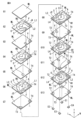
- FIG. 3 is an exploded perspective view showing a schematic example of the internal structure of a laminated inductor according to the present disclosure.
- the element body 10 is configured by stacking a plurality of magnetic layers ML in the height direction.
- the element body 10 may include a first coil C1 having a first winding portion W1, which will be described later, and a second coil C2 having a second winding portion W2.
- the element body 10 is configured by stacking the laminated groups G1 to G13 and forming the first external electrode E1 to the fourth external electrode E4 on the lower side of the laminated group G13.
- the boundaries between the layers of the laminated structure of the element body 10 may disappear.
- Each of the laminated groups G1 to G13 may be configured by stacking the same pattern multiple times.
- the multilayer group G1 has a magnetic layer ML and may form the second main surface 12 of the element body 10.
- the multilayer group G2 includes a magnetic layer ML, a second winding portion W2 formed by winding a conductor layer, and a fourth through hole (not shown).
- the multilayer group G2 may further include a fourth connection portion J4 connecting the second winding portion W2 and the fourth through hole, and a via hole (not shown) connecting to the second winding portion W2 of the multilayer group G4.
- the second winding portion W2 of the stacking group G2 has an oval shape in a top view.
- oval shape refers to a shape that has no corners in the inner peripheral portion of the winding portion except for the places avoided by the avoidance portion. Specifically, it refers to an egg shape, an elliptical shape, or an oval shape in which curved portions and straight portions smoothly continue together (oval track shape).
- the winding axis P of the second winding portion W2 may be offset from the center O of the element body 10 in a top view. In other words, the winding axis P of the coil and the center O of the element body 10 do not have to coincide.
- the one end S may be located on a straight line L1 connecting the fourth external electrode E4 and the third external electrode E3 when viewed from above.
- the one end S may be connected to a via hole V of the multilayer group G3.
- the other end F may be located on a straight line L2 connecting the fourth external electrode E4 and the first external electrode E1 when viewed from above.
- the fourth through hole (not shown) of the stacking group G2 may be electrically connected to the other end F of the second winding portion W2.
- electrically connected is not limited to a direct connection between the winding portion and the through hole, but is intended to allow for the presence of other elements such as an intervening object (e.g., a connection portion).
- the fourth through hole T4 may be located above the fourth external electrode E4.
- the fourth connection portion J4 of the stacking group G2 may be interposed between the second winding portion W2 and a fourth through hole (not shown).
- the shape of the fourth connection portion J4 in a top view may be linear. By using such a shape, the inner diameter of the second winding portion W2 can be maximized as much as possible, improving the characteristics of the inductor.
- the multilayer group G3 includes a magnetic layer ML, a via hole V that connects the second winding portions W2 adjacent to each other in the stacking direction, and a fourth through hole T4.
- the via hole V of the laminate group G3 may be arranged at a position that connects to one end S of the second winding portion W2 of the laminate group G2 described above.
- the via hole V of the laminate group G3 may be arranged adjacent to the fourth through hole T4 in a top view at a distance that ensures electrical insulation.
- the fourth through hole T4 of the stacking group G3 may be electrically connected to the fourth external electrode E4 by connecting the fourth through holes T4 of the stacking groups G2 and G4 adjacent to each other in the stacking direction. Therefore, the fourth through hole T4 may be disposed above the fourth external electrode E4. Furthermore, the fourth through hole T4 may have a shape that corresponds to the outer edge of the avoidance portion A, which will be described later, when viewed from above. In other words, the shape of the fourth through hole T4 may be such that the distance between it and the avoidance portion A is kept constant.
- the multilayer group G4 includes a magnetic layer ML, a second winding portion W2 formed by winding a conductor layer, and a fourth through hole T4.
- the multilayer group G4 may further include a via hole (not shown) that connects to the second winding portion W2 of the multilayer group G6.
- the second winding portion W2 of the laminate group G4 has an oval shape when viewed from above. Furthermore, when viewed from above, the second winding portion W2 of the laminate group G4 may at least partially overlap with the second winding portion W2 of the laminate group G2. Furthermore, the winding axis P of the second winding portion W2 may be offset from the center O of the element body 10 when viewed from above.
- the one end S and the other end F may be arranged on a straight line L1 connecting the fourth external electrode E4 and the third external electrode E3 when viewed from above. Furthermore, the one end S may be arranged closer to the third external electrode E3 than the other end F.
- the one end S may be connected to the via hole V of the multilayer group G5 through a via hole. Furthermore, the other end F may be connected to the via hole V of the multilayer group G3.
- the second winding portion W2 of the laminate group G4 may include an avoidance portion A that avoids the fourth through hole T4.
- the avoidance portion A may have a shape that protrudes further toward the inner diameter side of the coil than the fourth through hole T4 when viewed from above (a shape that bulges toward the inside of the coil).
- the avoidance portion A may also be provided in one location in the second winding portion W2.
- the fourth through hole T4 of the stacking group G4 may be electrically connected to the fourth external electrode E4 by connecting the fourth through holes T4 of the stacking groups G3 and G5 adjacent to each other in the stacking direction. Therefore, the fourth through hole T4 may be disposed above the fourth external electrode E4. Furthermore, the fourth through hole T4 may have a shape that corresponds to the outer edge of the avoidance portion A when viewed from above.
- the multilayer group G5 includes a magnetic layer ML, a via hole V that connects the second winding portions W2 adjacent to each other in the stacking direction, and a fourth through hole T4.
- the via hole V of the laminate group G5 may be arranged at a position that connects to one end S of the second winding portion W2 of the laminate group G4 described above.
- the via hole V of the laminate group G5 may be arranged adjacent to the fourth through hole T4 in a top view at a distance that ensures electrical insulation.
- the second winding portion W2 of the laminate group G6 may include an avoidance portion A that avoids the fourth through hole T4.
- the avoidance portion A may have a shape that protrudes further toward the inner diameter side of the coil than the fourth through hole T4 when viewed from above.
- the avoidance portion A may also be provided in one location in the second winding portion W2.
- the third through hole (not shown) of the laminate group G6 is electrically connected to one end S of the second winding portion W2.
- the third through hole may be disposed above the third external electrode E3.
- the third connection portion J3 of the stacking group G6 may be interposed between the second winding portion W2 and the third through hole (not shown).
- the shape of the third connection portion J3 in a top view may be curved. By using such a shape, the second winding portion W2 and the third through hole can be appropriately connected.
- the curvature of the third connection portion J3 of the laminate group G6 may be smaller than the curvature of the oval-shaped second winding portion W2.
- the third connection portion J3 may have a gentler curve than the second winding portion W2.
- the fourth through hole T4 of the stacking group G6 may be electrically connected to the fourth external electrode E4 by connecting the fourth through holes T4 of the stacking groups G5 and G7 adjacent to each other in the stacking direction. Therefore, the fourth through hole T4 may be disposed above the fourth external electrode E4. Furthermore, the fourth through hole T4 may have a shape that corresponds to the outer edge of the avoidance portion A when viewed from above.
- the multilayer group G7 may include a magnetic layer ML, a third through hole T3, and a fourth through hole T4.
- the third through hole T3 of the stacking group G7 may be electrically connected to the third through holes T3 of the stacking groups G6 and G8 adjacent to each other in the stacking direction, and may be electrically connected to the third external electrode E3. Therefore, the third through hole T3 may be disposed on the third external electrode E3.
- the fourth through hole T4 of the stacking group G7 may be electrically connected to the fourth through holes T4 of the stacking groups G6 and G8 adjacent to each other in the stacking direction, and may be electrically connected to the fourth external electrode E4. Therefore, the fourth through hole T4 may be disposed above the fourth external electrode E4.
- the one end S may be located on a straight line L4 connecting the second external electrode E2 and the first external electrode E1 when viewed from above.
- the one end S may also be connected to a via hole V of the multilayer group G9.
- the other end F may be located on a straight line L3 connecting the third external electrode E3 and the second external electrode E2 when viewed from above or inside the straight line L3.
- the second connection portion J2 of the stacking group G8 may be interposed between the first winding portion W1 and the second through hole (not shown).
- the shape of the second connection portion J2 in a top view may be curved. By using such a shape, the first winding portion W1 and the second through hole can be appropriately connected.
- the curvature of the second connection portion J2 of the laminate group G8 may be smaller than the curvature of the oval-shaped first winding portion W1.
- the second connection portion J2 may have a gentler curve than the first winding portion W1.
- the third through hole T3 of the stacking group G8 may be electrically connected to the third external electrode E3 by connecting the third through holes T3 of the stacking groups G7 and G9 adjacent to each other in the stacking direction. Therefore, the third through hole T3 may be disposed above the third external electrode E3.
- the fourth through hole T4 of the stacking group G8 may be electrically connected to the fourth external electrode E4 by connecting the fourth through holes T4 of the stacking groups G7 and G9 adjacent to each other in the stacking direction. Therefore, the fourth through hole T4 may be disposed above the fourth external electrode E4. Furthermore, the fourth through hole T4 may have a shape that corresponds to the outer edge of the avoidance portion A when viewed from above.
- the multilayer group G9 may include a magnetic layer ML, a via hole V connecting the first winding portions W1 adjacent in the stacking direction, a second through hole T2, a third through hole T3, and a fourth through hole T4.
- the second through hole T2 of the stacking group G9 may be electrically connected to the second external electrode E2 by connecting the second through holes T2 of the stacking groups G8 and G10 adjacent to each other in the stacking direction. Therefore, the second through hole T2 may be disposed above the second external electrode E2.
- the third through hole T3 of the stacking group G9 may be electrically connected to the third external electrode E3 by connecting the third through holes T3 of the stacking groups G8 and G10 adjacent in the stacking direction. Therefore, the third through hole T3 may be disposed above the third external electrode E3.
- the fourth through hole T4 of the stacking group G9 may be electrically connected to the fourth external electrode E4 by connecting the fourth through holes T4 of the stacking groups G8 and G10 adjacent to each other in the stacking direction. Therefore, the fourth through hole T4 may be disposed above the fourth external electrode E4. Furthermore, the fourth through hole T4 may have a shape that corresponds to the outer edge of the avoidance portion A when viewed from above.
- the first winding portion W1 of the laminate group G10 has an oval shape when viewed from above. Furthermore, when viewed from above, the first winding portion W1 of the laminate group G10 may at least partially overlap with the first winding portion W1 of the laminate group G8. Furthermore, the winding axis P of the first winding portion W1 may be offset from the center O of the element body 10 when viewed from above.
- the one end S and the other end F may be arranged on a straight line L4 connecting the second external electrode E2 and the first external electrode E1 when viewed from above. Furthermore, the one end S may be arranged closer to the first external electrode E1 than the other end F.
- the one end S may also be connected to the via hole V of the multilayer group G11 through a via hole.
- the other end F may be connected to the via hole V of the multilayer group G9.
- the first winding portion W1 of the laminate group G10 may include an avoidance portion A that avoids the fourth through hole T4.
- the avoidance portion A may have a shape that protrudes further toward the inner diameter side of the coil than the fourth through hole T4 when viewed from above.
- the avoidance portion A may be provided in one location in the first winding portion W1.
- the second through hole T2 of the stacking group G10 may be electrically connected to the second external electrode E2 by connecting the second through holes T2 of the stacking groups G9 and G11 adjacent to each other in the stacking direction. Therefore, the second through hole T2 may be disposed above the second external electrode E2.
- the third through hole T3 of the stacking group G10 may be electrically connected to the third external electrode E3 by connecting the third through holes T3 of the stacking groups G9 and G11 adjacent to each other in the stacking direction. Therefore, the third through hole T3 may be disposed above the third external electrode E3.
- the fourth through hole T4 of the stacking group G10 may be electrically connected to the fourth external electrode E4 by connecting the fourth through holes T4 of the stacking groups G9 and G11 adjacent to each other in the stacking direction. Therefore, the fourth through hole T4 may be disposed above the fourth external electrode E4. Furthermore, the fourth through hole T4 may have a shape that corresponds to the outer edge of the avoidance portion A when viewed from above.
- the multilayer group G11 may include a magnetic layer ML, a via hole V connecting the first winding portions W1 adjacent in the stacking direction, a second through hole T2, a third through hole T3, and a fourth through hole T4.
- the via hole V of the laminate group G11 may be arranged at a position that connects to one end S of the first winding portion W1 of the laminate group G10 described above.
- the via hole V of the laminate group G11 may be arranged adjacent to the second through hole T2 in a top view at a distance that ensures electrical insulation.
- the second through hole T2 of the stacking group G11 may be electrically connected to the second external electrode E2 by connecting the second through holes T2 of the stacking groups G10 and G12 adjacent to each other in the stacking direction. Therefore, the second through hole T2 may be disposed above the second external electrode E2.
- the third through hole T3 of the stacking group G11 may be electrically connected to the third external electrode E3 by connecting the third through holes T3 of the stacking groups G10 and G12 adjacent in the stacking direction. Therefore, the third through hole T3 may be disposed above the third external electrode E3.
- the fourth through hole T4 of the stacking group G11 may be electrically connected to the fourth external electrode E4 by connecting the fourth through holes T4 of the stacking groups G10 and G12 adjacent in the stacking direction. Therefore, the fourth through hole T4 may be disposed above the fourth external electrode E4. Furthermore, the fourth through hole T4 may have a shape that corresponds to the outer edge of the avoidance portion A when viewed from above.
- the multilayer group G12 includes a magnetic layer ML, a first winding portion W1 formed by winding a conductor layer, a first through hole (not shown), a second through hole T2, a third through hole T3, and a fourth through hole T4.
- the multilayer group G12 may further include a first connection portion J1 that connects the first winding portion W1 and the first through hole.
- the first winding portion W1 of the laminate group G12 has an oval shape when viewed from above. Furthermore, when viewed from above, the first winding portion W1 of the laminate group G12 may at least partially overlap with the first winding portion W1 of the laminate group G10. Furthermore, the winding axis P of the first winding portion W1 may be offset from the center O of the element body 10 when viewed from above.
- the one end S may be provided on a straight line L2 connecting the fourth external electrode E4 and the first external electrode E1 when viewed from above.
- the other end F may be provided on a straight line L4 connecting the second external electrode E2 and the first external electrode E1 when viewed from above.
- the other end F may also be connected to a via hole V of the multilayer group G11.
- the first winding portion W1 of the laminate group G12 may include an avoidance portion A that avoids the fourth through hole T4.
- the avoidance portion A may be provided in one location in the first winding portion W1.
- the avoidance portion A may have a shape that protrudes further toward the inner diameter side of the coil than the fourth through hole T4 when viewed from above.
- the first through hole (not shown) of the laminate group G12 is electrically connected to one end S of the first winding portion W1.
- the first through hole T1 may be disposed above the first external electrode E1.
- the first connection portion J1 of the laminate group G12 may be interposed between the first winding portion W1 and a first through hole (not shown).
- the shape of the first connection portion J1 in a top view may be linear. By using such a shape, the inner diameter of the second winding portion W2 can be maximized as much as possible, improving the characteristics of the inductor.
- the second through hole T2 of the stacking group G12 may be electrically connected to the second external electrode E2 by connecting the second through holes T2 of the stacking groups G11 and G13 adjacent to each other in the stacking direction. Therefore, the second through hole T2 may be disposed above the second external electrode E2.
- the third through hole T3 of the stacking group G12 may be electrically connected to the third external electrode E3 by connecting the third through holes T3 of the stacking groups G11 and G13 adjacent to each other in the stacking direction. Therefore, the third through hole T3 may be disposed above the third external electrode E3.
- the multilayer group G13 may include a magnetic layer ML, a first through hole T1, a second through hole T2, a third through hole T3, and a fourth through hole T4.
- the areas of the first through holes T1 to the fourth through holes T4 of the multilayer groups G1 to G13 in a top view may be substantially the same.
- connection portion (second connection portion J2 and third connection portion J3) on the -W direction side in top view is curved
- the connection portion (first connection portion J1 and fourth connection portion J4) on the +W direction side is linear in top view, so that the winding axis P of the first winding portion W1 and the second winding portion W2 can be appropriately shifted from the center O of the element body in top view as described above.
- connection portion on the +W side has a linear shape when viewed from above, the amount of wiring that protrudes from the first winding portion W1 and the second winding portion W2 beyond the avoidance portion A can be reduced, further reducing the element area.
- the third winding portion W3 may be electrically connected to a fifth external electrode (not shown) and a sixth external electrode E6. Specifically, the end of the third winding portion W3 closest to the bottom surface may be electrically connected to the fifth external electrode by a fifth through hole (not shown). In addition, the other end of the third winding portion W3 may be connected to the sixth external electrode E6 by a sixth through hole T6.
- the sixth winding portion W6 may be electrically connected to the eleventh external electrode E11 and the twelfth external electrode E12. Specifically, the end of the sixth winding portion W6 closest to the bottom surface may be connected to the eleventh external electrode E11 by the eleventh through hole T11. The other end of the sixth winding portion W6 may be connected to the twelfth external electrode E12 by the twelfth through hole T12.
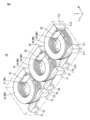
- the first winding portion W1 to the sixth winding portion W6 are oval in shape when viewed from above, the first winding portion W1 and/or the second winding portion W2 are provided with a first avoidance portion A1 that avoids any one of the first through-hole T1 to the fourth through-hole, the third winding portion W3 and/or the fourth winding portion W4 are provided with a second avoidance portion A2 that avoids any one of the fifth through-hole to the eighth through-hole T8, and the fifth winding portion W5 and/or the sixth winding portion W6 are provided with a third avoidance portion A3 that avoids any one of the ninth through-hole to the twelfth through-hole T12.
- the first avoidance portion A1 avoids the fourth through-hole T4
- the second avoidance portion A2 avoids the eighth through-hole T8
- the third avoidance portion A3 avoids the twelfth through-hole T12.
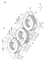
- FIG. 5 is a perspective view that shows a schematic diagram of a modified example of the laminated inductor array of the present disclosure. Note that this modified example differs from the laminated inductor array described above in terms of the positional relationship between the first avoidance portion A1 and the third avoidance portion and the second avoidance portion A2. The other configurations are as described for the laminated inductor array described above.
- the second avoidance portion A2 is not arranged along the same side of the element body 10 as the first avoidance portion A1 and the third avoidance portion.
- the first avoidance portion A1 and the third avoidance portion may be arranged on the +W direction side of the element body 10
- the second avoidance portion A2 may be arranged on the -W direction side of the element body 10 rotated 180 degrees (i.e., the first avoidance portion A1 and the second avoidance portion A2 may be alternated).
- the magnetic flux direction is reversed between the first winding portion W1 and the fifth winding portion W5 adjacent to the second winding portion W2, or between the second winding portion W2 and the sixth winding portion W6 adjacent to the fourth winding portion W4, reducing the bias of the magnetic flux and making it even more difficult for magnetic saturation to occur. Therefore, the DC superposition characteristics of the laminated inductor can be improved.
- laminated inductor arrays 1B and 1C three laminated inductors 1A are arranged in an array, but two arrays or four or more arrays are also acceptable.
- Example 1 which is the laminated inductor of the present disclosure
- Comparative Example 1 which is a conventional laminated inductor
- Example 1 As shown in Figure 2, the first winding portion W1 and the second winding portion W2 have an oval shape when viewed from above, and the first winding portion W1 and the second winding portion W2 have an avoidance portion A that avoids the fourth through hole T4 and have two corner portions Z (see Figure 6).
- Size of element 10 (see FIG. 2): L direction: 1.6 mm ⁇ W direction: 2.0 mm ⁇ T direction: 1.0 mm Width d of the first winding portion (or the second winding portion) as viewed from above (see FIG. 2): 0.38 mm Height of the first winding portion (or the second winding portion) (height (thickness) of the first and second winding portions W1 and W2 in each stacking group in FIG. 3): 0.085 mm Interlayer gap of the first winding portion (or the second winding portion) (the distance between the lamination groups in each lamination group in FIG. 3): 0.01 mm Number of turns in the first winding section (or the second winding section): 2.5 turns
- Comparative Example 1 As shown in Figure 7A, the first winding portion and the second winding portion have a substantially rectangular shape when viewed from above, and the first winding portion and the second winding portion have an avoidance portion that avoids the second through hole, an avoidance portion that avoids the third through hole, and an avoidance portion that avoids the fourth through hole, and five corners Z are provided (see Figure 7A).
- the magnetic field analysis simulation was performed using Femtet (registered trademark) made by Murata Software Co., Ltd.
- Fig. 9 is a graph showing the simulation results of the DC superimposition characteristics of Example 1 and Comparative Example 1.
- the laminated inductor and laminated inductor array of the present disclosure include the following aspects. ⁇ 1> A base body having a laminated magnetic layer and a rectangular bottom surface; a first external electrode, a second external electrode, a third external electrode and a fourth external electrode provided at four corners of the bottom surface of the element body; a first winding section in which a plurality of conductor layers disposed within the element body are connected in a stacking direction and which has a winding axis in the stacking direction; a second winding section located above the first winding section in the stacking direction, in which a plurality of conductor layers disposed within the element body are connected in the stacking direction, and which has a winding axis in the stacking direction; a first through hole that electrically connects one end of the first winding portion and the first external electrode and extends in the stacking direction; a second through hole that electrically connects the other end of the first winding portion and the second external electrode and extends in the stacking direction; a third through hole
- the length of the through hole in the stacking direction satisfies the following relationship:
- the laminated inductor described in ⁇ 1> wherein: a length of the fourth through hole>a length of the third through hole; a length of the third through hole>a length of the second through hole; and a length of the second through hole>a length of the first through hole, the avoidance portion avoiding the fourth through hole.
- ⁇ 3> The laminated inductor according to ⁇ 1> or ⁇ 2>, wherein the winding axis of the first winding portion and the winding axis of the second winding portion are offset from the center of the element body in a direction intersecting the lamination direction.
- ⁇ 4> The laminated inductor according to ⁇ 3>, wherein the direction of the deviation of the winding axis is a direction intersecting the lamination direction in a top view and is a side on which the avoidance portion is provided.
- One end of the first winding portion and the first through hole are connected via a linear first connection portion, the other end of the first winding portion and the second through hole are connected via a curved second connection portion, one end of the second winding portion and the third through hole are connected via a curved third connection portion,
- ⁇ 6> The laminated inductor according to ⁇ 5>, wherein the curvature of the second connection portion and the third connection portion is smaller than the curvature of the first winding portion and the second winding portion.
- ⁇ 7> The laminated inductor according to any one of ⁇ 1> to ⁇ 6>, wherein the second external electrode and the third external electrode are arranged along one side of a bottom surface of the rectangular body.
- ⁇ 9> The laminated inductor array according to ⁇ 8>, wherein the first avoidance portion and the second avoidance portion are not arranged along one side of the element body.
- This disclosure can be used for laminated inductors and laminated inductor arrays that have smaller element areas and improved DC bias characteristics.
- Multilayer inductor 1B, 1C Multilayer inductor array 10: Element body 11 First main surface 12 Second main surface 13 First end surface 14 Second end surface 15 First side surface 16 Second side surface A Avoidance portion A1 First avoidance portion A2 Second avoidance portion C Coils C1 to C2 First coil to second coil J1 to J4 First connection portion to fourth connection portion E1 to E12 First external electrode to twelfth external electrode T1 to T12 First through hole to twelfth through hole V Via hole W1 First winding portion W2 Second winding portion ML Magnetic layer Z Corner portion DW Lead-out wiring P Winding axis O Center of element body
Landscapes
- Engineering & Computer Science (AREA)
- Power Engineering (AREA)
- Microelectronics & Electronic Packaging (AREA)
- Coils Or Transformers For Communication (AREA)
Priority Applications (3)
| Application Number | Priority Date | Filing Date | Title |
|---|---|---|---|
| CN202480029668.0A CN121039762A (zh) | 2023-09-06 | 2024-05-17 | 层叠电感器以及层叠电感器阵列 |
| JP2025544135A JPWO2025052729A1 (https=) | 2023-09-06 | 2024-05-17 | |
| US19/418,083 US20260112532A1 (en) | 2023-09-06 | 2025-12-12 | Multilayer inductor and multilayer inductor array |
Applications Claiming Priority (2)
| Application Number | Priority Date | Filing Date | Title |
|---|---|---|---|
| JP2023-144455 | 2023-09-06 | ||
| JP2023144455 | 2023-09-06 |
Related Child Applications (1)
| Application Number | Title | Priority Date | Filing Date |
|---|---|---|---|
| US19/418,083 Continuation US20260112532A1 (en) | 2023-09-06 | 2025-12-12 | Multilayer inductor and multilayer inductor array |
Publications (1)
| Publication Number | Publication Date |
|---|---|
| WO2025052729A1 true WO2025052729A1 (ja) | 2025-03-13 |
Family
ID=94923405
Family Applications (1)
| Application Number | Title | Priority Date | Filing Date |
|---|---|---|---|
| PCT/JP2024/018328 Pending WO2025052729A1 (ja) | 2023-09-06 | 2024-05-17 | 積層インダクタおよび積層インダクタアレイ |
Country Status (4)
| Country | Link |
|---|---|
| US (1) | US20260112532A1 (https=) |
| JP (1) | JPWO2025052729A1 (https=) |
| CN (1) | CN121039762A (https=) |
| WO (1) | WO2025052729A1 (https=) |
Citations (4)
| Publication number | Priority date | Publication date | Assignee | Title |
|---|---|---|---|---|
| JP2006093603A (ja) * | 2004-09-27 | 2006-04-06 | Mitsubishi Materials Corp | 積層型コモンモードチョークコイルアレイ |
| JP2014138168A (ja) * | 2013-01-18 | 2014-07-28 | Tdk Corp | 積層コイル部品 |
| JP2020061411A (ja) * | 2018-10-05 | 2020-04-16 | 株式会社村田製作所 | 積層型コイルアレイ |
| JP2021052076A (ja) * | 2019-09-25 | 2021-04-01 | Tdk株式会社 | コイル部品及びその製造方法 |
-
2024
- 2024-05-17 WO PCT/JP2024/018328 patent/WO2025052729A1/ja active Pending
- 2024-05-17 JP JP2025544135A patent/JPWO2025052729A1/ja active Pending
- 2024-05-17 CN CN202480029668.0A patent/CN121039762A/zh active Pending
-
2025
- 2025-12-12 US US19/418,083 patent/US20260112532A1/en active Pending
Patent Citations (4)
| Publication number | Priority date | Publication date | Assignee | Title |
|---|---|---|---|---|
| JP2006093603A (ja) * | 2004-09-27 | 2006-04-06 | Mitsubishi Materials Corp | 積層型コモンモードチョークコイルアレイ |
| JP2014138168A (ja) * | 2013-01-18 | 2014-07-28 | Tdk Corp | 積層コイル部品 |
| JP2020061411A (ja) * | 2018-10-05 | 2020-04-16 | 株式会社村田製作所 | 積層型コイルアレイ |
| JP2021052076A (ja) * | 2019-09-25 | 2021-04-01 | Tdk株式会社 | コイル部品及びその製造方法 |
Also Published As
| Publication number | Publication date |
|---|---|
| CN121039762A (zh) | 2025-11-28 |
| US20260112532A1 (en) | 2026-04-23 |
| JPWO2025052729A1 (https=) | 2025-03-13 |
Similar Documents
| Publication | Publication Date | Title |
|---|---|---|
| JP3621300B2 (ja) | 電源回路用積層インダクタ | |
| JP4821908B2 (ja) | 積層型電子部品及びこれを備えた電子部品モジュール | |
| JP3686908B2 (ja) | 積層型コイル部品及びその製造方法 | |
| JP7032039B2 (ja) | 積層コイル部品 | |
| KR101843283B1 (ko) | 코일 전자 부품 | |
| JP7044508B2 (ja) | 磁気結合型コイル部品 | |
| US20140132385A1 (en) | Multilayer chip inductor and production method for same | |
| JP2003017326A (ja) | 積層型インダクタ | |
| WO2009125656A1 (ja) | 電子部品 | |
| CN107871585B (zh) | 电子部件 | |
| KR20050059214A (ko) | 적층 코일 부품 및 그 제조방법 | |
| JP2005150168A (ja) | 積層コイル部品 | |
| CN108987036A (zh) | 线圈部件 | |
| JP5008926B2 (ja) | 積層型インダクタ及び積層型インダクタのインダクタンス調整方法 | |
| US20200411228A1 (en) | Laminated coil component | |
| JP7168312B2 (ja) | 磁気結合型コイル部品 | |
| CN113903546A (zh) | 层叠线圈部件 | |
| WO2025052729A1 (ja) | 積層インダクタおよび積層インダクタアレイ | |
| JP2003217935A (ja) | 積層インダクタアレイ | |
| JP4400430B2 (ja) | 積層型インダクタ | |
| WO2024161683A1 (ja) | 積層型コイルおよび積層型コイルアレイ | |
| US20250157720A1 (en) | Laminated inductor | |
| CN114974801A (zh) | 层叠线圈部件 | |
| US20250029771A1 (en) | Multilayer inductor and multilayer inductor array | |
| JP4400092B2 (ja) | 表面実装型インダクタ |
Legal Events
| Date | Code | Title | Description |
|---|---|---|---|
| 121 | Ep: the epo has been informed by wipo that ep was designated in this application |
Ref document number: 24862386 Country of ref document: EP Kind code of ref document: A1 |
|
| ENP | Entry into the national phase |
Ref document number: 2025544135 Country of ref document: JP Kind code of ref document: A |
|
| WWE | Wipo information: entry into national phase |
Ref document number: 2025544135 Country of ref document: JP |