WO2025041367A1 - 電流センサ - Google Patents
電流センサ Download PDFInfo
- Publication number
- WO2025041367A1 WO2025041367A1 PCT/JP2024/006260 JP2024006260W WO2025041367A1 WO 2025041367 A1 WO2025041367 A1 WO 2025041367A1 JP 2024006260 W JP2024006260 W JP 2024006260W WO 2025041367 A1 WO2025041367 A1 WO 2025041367A1
- Authority
- WO
- WIPO (PCT)
- Prior art keywords
- thin plate
- substrate
- magnetic shield
- current sensor
- plate member
- Prior art date
- Legal status (The legal status is an assumption and is not a legal conclusion. Google has not performed a legal analysis and makes no representation as to the accuracy of the status listed.)
- Pending
Links
Images





Classifications
-
- G—PHYSICS
- G01—MEASURING; TESTING
- G01R—MEASURING ELECTRIC VARIABLES; MEASURING MAGNETIC VARIABLES
- G01R1/00—Details of instruments or arrangements of the types included in groups G01R5/00 - G01R13/00 and G01R31/00
- G01R1/02—General constructional details
- G01R1/18—Screening arrangements against electric or magnetic fields, e.g. against earth's field
-
- G—PHYSICS
- G01—MEASURING; TESTING
- G01R—MEASURING ELECTRIC VARIABLES; MEASURING MAGNETIC VARIABLES
- G01R15/00—Details of measuring arrangements of the types provided for in groups G01R17/00 - G01R29/00, G01R33/00 - G01R33/26 or G01R35/00
- G01R15/14—Adaptations providing voltage or current isolation, e.g. for high-voltage or high-current networks
- G01R15/20—Adaptations providing voltage or current isolation, e.g. for high-voltage or high-current networks using galvano-magnetic devices, e.g. Hall-effect devices, i.e. measuring a magnetic field via the interaction between a current and a magnetic field, e.g. magneto resistive or Hall effect devices
-
- G—PHYSICS
- G01—MEASURING; TESTING
- G01R—MEASURING ELECTRIC VARIABLES; MEASURING MAGNETIC VARIABLES
- G01R19/00—Arrangements for measuring currents or voltages or for indicating presence or sign thereof
- G01R19/0092—Measuring current only
-
- G—PHYSICS
- G01—MEASURING; TESTING
- G01R—MEASURING ELECTRIC VARIABLES; MEASURING MAGNETIC VARIABLES
- G01R33/00—Arrangements or instruments for measuring magnetic variables
- G01R33/02—Measuring direction or magnitude of magnetic fields or magnetic flux
Definitions
- the present invention relates to a current sensor equipped with a magnetic shield that measures the current to be measured flowing through a bus bar.
- Patent Document 1 describes a current sensor having a pair of magnetic shield plates sandwiching a conductor and a magnetoelectric conversion element, which aims to reduce the wasted space between the pair of magnetic shield plates and improve the accuracy of the current sensor.
- the pair of magnetic shields in the current sensor described in the document are integrally formed with a resin package as a housing, together with a sensor substrate and a bus bar.
- the magnetic shield plates and the housing are integrally formed as in this current sensor, it is difficult to reduce the size, weight, and cost of the current sensor.
- Patent document 2 describes a current sensor in which a pair of magnetic shields that block external magnetic fields are used for the purpose of high-precision current detection, and the magnetic shield on the magnetic detection side equipped with a magnetic detection element is fixed to a circuit board by a fixing member.
- the current sensor described in Patent Document 2 is more advantageous than the current sensor described in Patent Document 1 in terms of size, weight, and cost reduction because the magnetic shield installed on the magnetic detection unit side is configured separately from the housing.
- the relative positions of the magnetic shield and the circuit board on which the magnetic detection element is provided are fixed with fixing members inserted into fixing holes provided at the four corners of the magnetic shield. That is, the fixing holes of the magnetic shield are overlapped with the through holes formed in the circuit board, and fixing members are inserted thereto to fix the magnetic shield to the circuit board. In this way, the magnetic shield is placed at a predetermined position on the circuit board based on the position of the hole. Therefore, an object of the present invention is to provide a current sensor in which a magnetic shield, which is constructed separately from the housing, can be easily positioned at a predetermined position on a board on which a magnetic detection unit is provided when fixing the magnetic shield to the board.
- the present invention has the following configuration. a first reference portion for positioning the first magnetic shield from a first surface facing the substrate, the substrate having an engagement portion engageable with the protrusion and a second reference portion for positioning, the case having a third reference portion for positioning, and wherein when the protrusion and the engagement portion are engaged with each other, the first reference portion, the second reference portion, and the third reference portion are aligned on a straight line parallel to a stacking direction of the first magnetic shield, the substrate, and the case.
- the first magnetic shield may be formed by laminating a plurality of thin plate members, and the protruding portion may be a press joint formed by crimping the plurality of thin plate members in a lamination direction.
- the press joint formed when crimping the first magnetic shield which is made up of multiple laminated thin plate members, as a protrusion and engaging it with the engaging portion of the substrate, it is possible to reduce component processing costs and labor, and suppress manufacturing costs.
- the first reference portion may be provided on a first thin plate member adjacent to the substrate, among the plurality of thin plate members included in the first magnetic shield.
- a plurality of pairs of the protrusions and the engagement portions may be provided. By providing a plurality of pairs of protrusions and engagement portions and engaging each pair, it becomes easy to position the first magnetic shield and the substrate, and the positioned state can be maintained.
- the first reference portion may be a shield hole that penetrates the first magnetic shield
- the second reference portion may be a board hole that penetrates the board
- the third reference portion may be a fixing boss having a stopper portion at a tip of the fixing boss, and when the fixing boss is inserted into the shield hole and the board hole, the first magnetic shield and the board may be fixed to the case by the stopper portion.
- the first magnetic shield may be formed by stacking a plurality of thin plate members, and the retaining portion may be in contact with an exposed portion of a second surface of the thin plate member other than the second thin plate member that is the furthest away from the substrate in the stacking direction.
- the first magnetic shield may have a hole or a notch formed continuously from the second thin plate member to the third thin plate member along the stacking direction, and the second surface exposed from the hole or the notch may be the exposed portion.
- the case may include a fixing screw, the first reference portion being a shield hole penetrating the first magnetic shield, the second reference portion being a board hole penetrating the board, and the third reference portion being a screw hole capable of screwing into the fixing screw, and the first magnetic shield and the board may be fixed to the case by the screw head of the fixing screw with the fixing screw inserted into the shield hole and the board hole.
- the first magnetic shield, the substrate and the case can be fixed in a stacked state in a predetermined position by inserting the fixing screw through the shield hole and the substrate hole and fixing the first magnetic shield and the substrate to the case with the screw head of the fixing screw.
- the first magnetic shield may be formed by stacking a plurality of thin plate members, and the screw head may be in contact with an exposed portion of a second surface of a thin plate member other than a second thin plate member that is the furthest away from the substrate in the stacking direction.
- the first magnetic shield may have a hole or a notch formed continuously from the second thin plate member to the third thin plate member along the stacking direction, and the second surface exposed from the hole or the notch may be the exposed portion.
- the first magnetic shield may be formed by stacking a plurality of thin plate members, and among the plurality of thin plate members of the first magnetic shield, the first thin plate member adjacent to the substrate may have the exposed portion exposed on the second surface opposite to the first surface facing the substrate, and the exposed portion may form part of a step portion or a recessed portion.
- the above configuration makes the length of the fixing boss or fixing screw shorter than when the retaining portion or screw head is located on the second surface of the second thin plate member of the first magnetic shield. This makes it easier to stack the first magnetic shield, and also makes it possible to more firmly fix the first magnetic shield and the board to the case.
- the present invention makes it easy to align the first magnetic shield with the substrate, providing a current sensor that can be easily positioned at a predetermined position on the substrate when the magnetic shield, which is constructed separately from the housing, is fixed to the substrate on which the magnetic detection unit is provided.
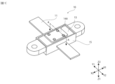
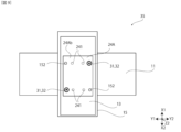
- FIG. 1 is a perspective view illustrating a schematic appearance of a current sensor according to a first embodiment
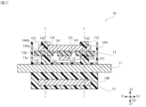
- 2 is a cross-sectional view showing a schematic configuration of a main part of a current sensor taken along line AA in FIG. 1
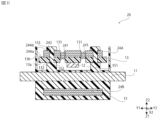
- 3 is a cross-sectional view illustrating a schematic configuration of a modified example of the current sensor of FIG. 2.
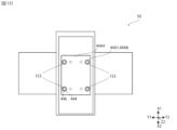
- FIG. 4 is a plan view of the current sensor of FIG. 3 .
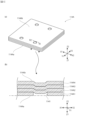
- 1 is an explanatory diagram of a structure of a magnetic shield having a conventional laminated structure.
- 5A and 5B are explanatory diagrams of a structure of a magnetic shield having a laminated structure in the current sensor of the present invention.
- 4 is a cross-sectional view illustrating a schematic configuration of another modified example of the current sensor of FIG. 2.
- FIG. 4 is a cross-sectional view illustrating a schematic configuration of another modified example of the current sensor of FIG. 2.
- FIG. 9 is a plan view illustrating a schematic configuration of the current sensor of FIG. 8 .
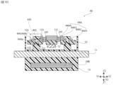
- FIG. 11 is a cross-sectional view illustrating a schematic configuration of a current sensor according to a second embodiment.
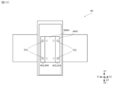
- FIG. 11 is a plan view illustrating a schematic configuration of a current sensor according to a second embodiment.
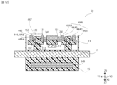
- 11 is a cross-sectional view illustrating a schematic configuration of a modified example of the current sensor of FIG. 10.
- FIG. 13 is a plan view illustrating a schematic configuration of the current sensor of FIG. 12 .
- FIG. 11 is a cross-sectional view illustrating a schematic configuration of a conventional current sensor.
- FIG. 2 is a cross-sectional view illustrating a schematic configuration of a current sensor without a cover.
- the width dimension direction of the bus bar is the X direction (third direction)
- the extension direction of the bus bar perpendicular to the X direction is the Y direction (second direction)
- the stacking direction of the bus bar and the magnetic sensor perpendicular to the X and Y directions is the Z direction (first direction).
- the X direction is the direction of the sensitivity axis of the magnetic sensor
- the Y and Z directions are perpendicular to the sensitivity axis.
- FIG. 14 is a cross-sectional view showing a schematic configuration of a conventional current sensor 100.
- the current sensor 100 shown in the figure includes a bus bar 101 through which the current to be measured flows, and a pair of parallel plate-type magnetic shields 104A and 104B that sandwich a magnetic sensor 102 provided on a substrate 103.
- the magnetic shield 104A is insert-molded into a cover 106
- the magnetic shield 104B is insert-molded into a case 105.
- FIG. 15 is a cross-sectional view showing a schematic configuration of a current sensor 110 without a cover.
- the current sensor 110 shown in the figure does not have a cover, and therefore, of the pair of magnetic shields 104A, 104B, the magnetic shield 104A is provided directly on the substrate 103.
- the current sensor of the present invention has a configuration for stably, easily and accurately determining the position of the magnetic shield 104A with respect to the substrate 103. An embodiment of the current sensor of the present invention will be described below.
- FIG. 1 is a perspective view showing a schematic external appearance of a current sensor 10 according to the present embodiment.
- FIG. 2 is a cross-sectional view showing a schematic configuration of a main part of the current sensor 10 taken along the line AA in FIG.
- the current sensor 10 includes a bus bar 11, a magnetic sensor 12, a substrate 13, a pair of flat plate-type magnetic shields 14A (first magnetic shield) and 14B (second magnetic shield), and a case 15.
- the magnetic shield 14A, substrate 13, magnetic sensor 12, bus bar 11, and magnetic shield 14B are stacked in this order in the Z2 to Z1 direction, and the bus bar 11 and magnetic shield 14B are provided in the case 15.
- the bus bar 11 is a conductor formed in a plate shape through which a current to be measured flows, and is made of, for example, copper, brass, aluminum, or the like.
- the magnetic sensor 12 detects the magnetism generated by the bus bar 11 when a current to be measured flows, and is provided on the surface 13a on the Z1 side of the substrate 13 so as to face the bus bar 11 in the Z direction.
- the detection surface of the magnetic sensor 12 faces the bus bar 11, and the sensitivity axis is parallel to the detection surface.
- the induced magnetic field generated near the detection surface of the magnetic sensor 12 when a current to be measured flows through the bus bar 11 contains a large component in the X direction. Therefore, by arranging the magnetic sensor 12 so that the sensitivity axis is parallel to the X direction, the magnetism generated by the bus bar 11 can be detected with high accuracy.
- a magnetoresistance effect element, a Hall element, etc. can be used as the detection element in the magnetic sensor 12. Note that the above-mentioned configuration is an example of a case where a magnetoresistance effect element is used as the detection element in the magnetic sensor 12. When using other detection elements, it is necessary to appropriately change the orientation of the detection surface, etc., and position the element.
- the magnetic shields 14A and 14B are arranged in the Z direction to sandwich the bus bar 11, the magnetic sensor 12, and the substrate 13, and are made of metal plates or the like.
- the magnetic shields 14A and 14B can suppress magnetic noise to the magnetic sensor 12, improving the measurement accuracy of the current sensor 10.
- Case 15 can be configured such that bus bar 11 and magnetic shield 14B are integrally formed by insert molding, for example.
- bus bar 11 may be provided by subsequently inserting bus bar 11 into case 15 in which magnetic shield 14B is integrally formed by insert molding.
- the magnetic shield 14A has a protrusion 141 that protrudes from an opposing surface 14Aa (first surface) that faces the substrate 13.
- the magnetic shield 14A has a hole 142 (shield hole) that penetrates in the Z direction as a first reference portion, through which a fixing boss 152 (described later) can be inserted.
- the substrate 13 has an engagement portion 131 that can engage with the protrusion 141 on the Z2 side facing surface 13b that faces the magnetic shield 14A, opposite the surface 13a on which the magnetic sensor 12 is provided. Since the engagement portion 131 only needs to be able to engage with the protrusion 141, instead of a hole that penetrates in the Z direction, it may be, for example, a recess that does not penetrate in the Z direction and corresponds to the shape of the protrusion 141.
- the current sensor 10 has multiple pairs of protrusions 141 and engagement portions 131, as shown in FIG. 2. By providing multiple pairs of protrusions 141 and engagement portions 131 and engaging each pair, it becomes easier to position the magnetic shield 14A and the substrate 13, and the aligned state can be reliably maintained.
- the substrate 13 has a hole 132 that penetrates in the Z direction as a second reference portion for positioning, into which a fixing boss 152 (described later) can be inserted.
- the magnetic shield 14A is positioned at a predetermined position on the substrate 13, so that the hole 142 in the magnetic shield 14A overlaps with the hole 132 (substrate hole) in the substrate 13.
- the hole 142 in the magnetic shield 14A and the hole 132 in the substrate 13 can be overlapped to form a continuous hole.
- the case 15 which is made of resin or the like, is integral with the insert-molded bus bar 11 and magnetic shield 14B.
- the case 15 has a storage recess 151 on the side facing the board 13.
- the storage recess 151 has a fixing boss 152 that protrudes in the Z2 direction as a third reference part for positioning.
- the holes 142 and 132 overlap when viewed along the Z direction.
- the fixing boss 152 By inserting the fixing boss 152, the positional relationship between the magnetic shield 14A and the substrate 13 and the case 15 is determined. In this state, the holes 142, 132 and the fixing boss 152 are arranged on a straight line L that is parallel to the stacking direction (Z direction) of the magnetic shield 14A, the substrate 13 and the case 15.
- the magnetic shield 14A and the substrate 13 are fixed to the case 15 by the retaining portion 153 provided at the Z2 side end (tip) of the fixing boss 152.
- the retaining portion 153 is formed by, for example, heat crimping the Z2 side end (tip) of the fixing boss 152 after the fixing boss 152 is inserted into the holes 142 and 132.
- the outer dimensions of the retaining portion 153 when viewed along the Z direction are larger than the inner diameters of the holes 142 and 132.
- the retaining portion 153 is also in close contact with the Z2 side surface 14Ab of the magnetic shield 14A. Therefore, the retaining portion 153 functions as a retaining member that holds the magnetic shield 14A and the substrate 13 in a predetermined position in the case 15.
- the positional relationship between the magnetic shield 14A, the board 13, and the case 15 is fixed by the retaining portion 153 with the magnetic sensor 12 on the board 13 positioned opposite the bus bar 11 in the storage recess 151.
- the current sensor 10 is arranged in a stacked manner with the magnetic shield 14A, board 13, bus bar 11, and magnetic shield 14B aligned in this order from the Z2 to Z1 direction, and the relative positions of the magnetic shield 14A, board 13, and case 15 can be determined.
- the board 13 and magnetic shield 14A in a predetermined position using the case 15 as a reference, it is possible to prevent the positions of the bus bar 11, magnetic shield 14A, and magnetic shield 14B from shifting relative to the magnetic sensor 12 provided on the board 13. This results in a current sensor 10 with good measurement accuracy in which errors due to positional shifts are suppressed.
- Modification 3 and 4 are a cross-sectional view and a plan view that typically show the configuration of a current sensor 20 that is a modification of the current sensor 10 of FIG.
- the current sensor 20 shown in these figures differs from the current sensor 10 in FIG. 2 in that, instead of the magnetic shields 14A, 14B made of a single metal plate, the current sensor 20 is provided with magnetic shields 24A, 24B made of multiple stacked metal plates of the same shape.
- FIG. 5 is an explanatory diagram of the structure of a magnetic shield 114A having a conventional laminated structure.
- the magnetic shield 114A has a structure in which multiple metal plates are stacked and hammered from the upper side (Z2 side) with a punch to crimp them.
- (b) shows the cross-sectional structure of the portion indicated by the line B-B in (a).
- a hole 1141 is provided in the metal plate 114A1 arranged on the lowest side (Z1 side), and when viewed along the Z direction, the part that overlaps with the hole 1141 is struck with a punch from the upper surface 114Ab to crimp the metal plates 114A1 to 114A4. At this time, the protrusion of the metal plate 114A2 adjacent to the metal plate 114A1 is pressed into the hole 1141. This prevents the formation of a convex portion protruding from the lower opposing surface 114Aa of the magnetic shield 114A, as indicated by the dashed line.
- FIG. 6 is an explanatory diagram of the structure of magnetic shield 24A with a laminated structure possessed by current sensor 20.
- magnetic shield 24A is the same as conventional magnetic shield 114A of FIG. 5 in that multiple metal plates are stacked and hammered from the top (Z2 side) with a punch to crimp them.
- Magnetic shield 24B may have a structure having a protrusion on one surface, similar to magnetic shield 24A, or may have a structure having no protrusion, similar to conventional magnetic shield 114A.
- FIG. 7 is a cross-sectional view that typically shows a current sensor 30 which is another modified example of the current sensor 20 of FIG.
- the current sensor 30 is different from the current sensor 10 in that it includes a fixing screw 31 and a screw hole 154 that can be screwed with the fixing screw 31 as a third reference portion is provided in the case 15.
- the inner diameters of the hole 242 (first shield hole) and the hole 132 are larger than the threaded portion of the fixing screw 31 and smaller than the outer diameter of the screw head 32.
- the magnetic shield 24A and the substrate 13 are fixed to the case 15 by the screw head 32 of the fixing screw 31 with the fixing screw 31 inserted through the hole 242 and the hole 132. This allows the magnetic shield 24A, the substrate 13, and the case 15 to be fixed in a stacked state in a predetermined position, with the fixing screw 31 acting as a holding member.
- FIG. 8 and 9 are a cross-sectional view and a plan view that show a schematic appearance of a current sensor 35, which is another variation of the current sensor 20 in FIG. 3.
- the current sensor 35 differs from the current sensor 20 in that the magnetic shield 24A, the substrate 13, and the case 15 are fixed by two fixing bosses 152 and two fixing screws 31.
- different fixing means may be used in combination to fix the magnetic shield 24A, the substrate 13, and the case 15.
- the different fixing means may be combined and arranged differently from that shown in Fig. 9.
- one fixing boss 152 may be combined with three fixing screws 31, or three fixing bosses 152 may be combined with one fixing screw 31.
- a configuration may be adopted in which a retaining portion 153 is provided at the tip of all or part of each fixing boss 152.
- FIG. 9 shows an example in which four fixing means are provided on the magnetic shield 24A, but the number of fixing means is not limited to four, and may be, for example, two, three, five or more.
- Second Embodiment 10 and 11 are a cross-sectional view and a plan view showing a schematic configuration of a current sensor 40 according to the present embodiment.
- the current sensor 40 differs from the current sensor 20 shown in FIG. 3 in that the current sensor 40 includes a magnetic shield 44A instead of the magnetic shield 24A.
- the magnetic shield 44A has a hole 442 as a first reference portion, which is provided only in the thin plate member 44A1 (first thin plate member) adjacent to the substrate 13 among the multiple thin plate members 44A1, 44A2, 44A3, and 44A4 that the magnetic shield 44A has.
- the thin plate member 44A1 has an exposed portion 444 that protrudes from the thin plate members 44A2, 44A3, and 44A4, and a hole 442 is provided in the exposed portion 444. Furthermore, when the Z2 side is considered to be the top, the exposed portion 444 is in a lower position (Z1 side) than the upper surface of the thin plate member 44A4, and a step portion 445 is formed.
- the retaining portion 153 can be disposed in the step portion 445. This makes it possible to reduce the amount of protrusion of the retaining portion 153 from the upper surface of the thin plate member 44A4 compared to when the retaining portion 153 is disposed on the upper surface of the thin plate member 44A4. In other words, it is possible to achieve a smaller size and lower height in the Z direction.
- the depth of the holes 442 in the stacking direction is shortened. This makes it easier to fit the holes 442 into the fixing bosses 152. Furthermore, the length of the fixing bosses 152 in the Z direction is shortened, improving the strength of the fixing bosses 152. Therefore, by fitting the holes 442 of the magnetic shield 44A and the holes 132 of the substrate 13 into the fixing bosses 152 of the case 15 and then fixing them, the magnetic shield 44A and the substrate 13 can be fixed more firmly to the case 15.
- the notch 443 is formed continuously from the thin plate member 44A4 (second thin plate member) that is the farthest from the substrate 13 in the stacking direction (Z direction) among the thin plate members 44A1 to 44A4, to the thin plate member 44A2 (third thin film member) adjacent to the thin plate member 44A1. That is, the notch 443 is formed in the thin plate members 44A2 to 44A4 other than the thin plate member 44A1, and the hole 442 is formed in the exposed portion 444 of the thin plate member 44A1 that is exposed when viewed from the surface 44Ab (second surface) of the magnetic shield 44A.
- the magnetic shield 44A has a hole or cutout 443 formed in the thin plate members 44A2 and 44A3 (third thin plate member) arranged between the thin plate member 44A1 (first thin plate member) and the thin plate member 44A4 (second thin plate member) in the stacking direction (Z direction) from the thin plate member 44A4 to the thin plate member 44A2.
- the surface 44Ab exposed from the cutout 443 is the exposed portion 444.
- a hole 442 serving as a first reference portion is provided only in the thin plate member 44A1 serving as the first thin plate member, and a step portion 445 is formed by the exposed portion 444 of the thin plate member 44A1 and the Y-direction end faces of the thin plate members 44A2 to 44A4. In other words, a part of the step portion 445 is formed by the exposed portion 444.
- the anti-slip portion 153 when viewed along the Z direction, the anti-slip portion 153 is brought into contact with the exposed portion 444, and the exposed portion 444 serves as a holding surface to hold the magnetic shield 44A and the substrate 13. In this way, the magnetic shield 44A can be fixed at a predetermined position on the case 15.
- the thin plate member 44A1 that contacts the substrate 13 is formed to be larger than the other thin plate members 44A2 to 44A4.
- a hole 442 shield hole is formed as a first reference portion in the exposed portion 444 of the thin plate member 44A1 that protrudes from the other thin plate members 44A2 to 44A4.
- thin plate members 44A2 to 44A4 have the same shape and size, and are all formed in a different shape from thin plate member 44A1.
- thin plate member 44A2 may be formed in the same shape and size as thin plate member 44A1
- thin plate members 44A3 to 44A4 may be formed in a different shape from thin plate member 44A1.
- hole 442 may be provided penetrating thin plate members 44A2 and 44A1.
- thin plate members large plate members
- thin plate member 44A1 when multiple thin plate members (large plate members) that are continuously stacked, including thin plate member 44A1, are formed to have the same shape and size and have portions that protrude from the remaining thin plate members (small plate members) including thin plate member 44A4, an exposed portion 444 may be formed on the Z2 side of the large plate member that is farthest from substrate 13, and a hole 442 that penetrates all of the large plate members may be formed in exposed portion 444.
- thin plate members 44A1 to 44A4 when viewed along the stacking direction, among thin plate members 44A1 to 44A4, one of thin plate members 44A1 to 44A3 is exposed. That is, an exposed portion 444 is formed on a thin plate member other than thin plate member 44A4, which is farthest from substrate 13 in the stacking direction, at 44Ab opposite opposing surface 44Aa that faces substrate 13. Then, magnetic shield 44A, substrate 13, and case 15 are fixed in place by contacting retaining portion 153 with exposed portion 444.
- the hole 442 is shorter than when the exposed portion 444 is formed in the thin plate member 44A4. This makes it easier to fit the hole 442 into the fixing boss 152. In addition, the fixing boss 152 is shorter, improving the strength of the current sensor 40.
- FIGs. 10 and 11 show a mode in which the retaining portions 153 are used for fastening
- screw heads 32 may be used in place of some or all of the retaining portions 153.
- fastening screws 31 are used instead of fastening bosses 152
- the length of the holes 442 in the Z direction is shortened, thereby reducing the workload of fastening the magnetic shield 44A and substrate 13 to the case 15 and improving the fastening strength.
- Modification 12 and 13 are a cross-sectional view and a plan view that typically show the configuration of a current sensor 50 that is a modification of the current sensor 40 of FIG.
- the magnetic shield 44A of the current sensor 50 shown in these figures differs from the current sensor 40 in that holes 446 are formed in the thin plate members 44A2 to 44A4 instead of the cutouts 443.
- a concave portion 447 is formed by the exposed portion 444 of the thin plate member 44A1 exposed from the hole 446 and the Y-direction end faces of the thin plate members 44A2 to 44A4.
- the magnetic shield 44A of the current sensor 50 has holes 446 formed continuously along the stacking direction from the thin plate members 44A4 to 44A2.
- the magnetic shield 44A and the substrate 13 are fixed to the case 15 by the retaining portion 153 coming into contact with the exposed portion 444 of the thin plate member 44A4 exposed from the hole 446.
- the exposed portion 444 may be formed on the Z2 side of the large plate member farthest from the substrate 13, and the hole 442 may be formed in the exposed portion 444, penetrating all of the large plate members.
- the length in the stacking direction of the hole 442 formed in the exposed portion 444 is shorter than when the exposed portion 444 is formed in the thin plate member 44A4. Therefore, the hole 442 can be easily fitted into the fixing boss 152, improving the strength of the current sensor 50.
- the present invention is useful, for example, as a current sensor for measuring the current flowing through equipment in order to control the power supply system of a vehicle or other device equipped with various devices.
Landscapes
- Physics & Mathematics (AREA)
- General Physics & Mathematics (AREA)
- Condensed Matter Physics & Semiconductors (AREA)
- Measuring Instrument Details And Bridges, And Automatic Balancing Devices (AREA)
Priority Applications (3)
| Application Number | Priority Date | Filing Date | Title |
|---|---|---|---|
| KR1020267000629A KR20260021049A (ko) | 2023-08-24 | 2024-02-21 | 전류 센서 |
| CN202480049305.3A CN121569201A (zh) | 2023-08-24 | 2024-02-21 | 电流传感器 |
| JP2025541298A JPWO2025041367A1 (cg-RX-API-DMAC7.html) | 2023-08-24 | 2024-02-21 |
Applications Claiming Priority (2)
| Application Number | Priority Date | Filing Date | Title |
|---|---|---|---|
| JP2023136639 | 2023-08-24 | ||
| JP2023-136639 | 2023-08-24 |
Publications (1)
| Publication Number | Publication Date |
|---|---|
| WO2025041367A1 true WO2025041367A1 (ja) | 2025-02-27 |
Family
ID=94731938
Family Applications (1)
| Application Number | Title | Priority Date | Filing Date |
|---|---|---|---|
| PCT/JP2024/006260 Pending WO2025041367A1 (ja) | 2023-08-24 | 2024-02-21 | 電流センサ |
Country Status (4)
| Country | Link |
|---|---|
| JP (1) | JPWO2025041367A1 (cg-RX-API-DMAC7.html) |
| KR (1) | KR20260021049A (cg-RX-API-DMAC7.html) |
| CN (1) | CN121569201A (cg-RX-API-DMAC7.html) |
| WO (1) | WO2025041367A1 (cg-RX-API-DMAC7.html) |
Citations (7)
| Publication number | Priority date | Publication date | Assignee | Title |
|---|---|---|---|---|
| WO2013114943A1 (ja) * | 2012-01-30 | 2013-08-08 | 株式会社オートネットワーク技術研究所 | 電流検出装置及び磁性体コア |
| JP2015083950A (ja) * | 2013-10-25 | 2015-04-30 | 株式会社フジクラ | 電流検出装置 |
| JP2015194349A (ja) * | 2014-03-31 | 2015-11-05 | 株式会社フジクラ | 電流検出装置 |
| WO2019181173A1 (ja) * | 2018-03-20 | 2019-09-26 | 株式会社デンソー | 電流センサ |
| US20190320524A1 (en) * | 2018-04-13 | 2019-10-17 | GM Global Technology Operations LLC | Pcba with point field detector and magnetic shielding array located on same side of a conductor |
| US20200267841A1 (en) * | 2019-02-15 | 2020-08-20 | Lg Electronics Inc. | Printed circuit board assembly |
| WO2021241586A1 (ja) * | 2020-05-27 | 2021-12-02 | アルプスアルパイン株式会社 | 電流センサ |
Family Cites Families (2)
| Publication number | Priority date | Publication date | Assignee | Title |
|---|---|---|---|---|
| JP6149885B2 (ja) | 2015-03-18 | 2017-06-21 | トヨタ自動車株式会社 | 電流センサ |
| JP6536553B2 (ja) | 2016-12-12 | 2019-07-03 | 株式会社デンソー | 電流センサ |
-
2024
- 2024-02-21 JP JP2025541298A patent/JPWO2025041367A1/ja active Pending
- 2024-02-21 WO PCT/JP2024/006260 patent/WO2025041367A1/ja active Pending
- 2024-02-21 CN CN202480049305.3A patent/CN121569201A/zh active Pending
- 2024-02-21 KR KR1020267000629A patent/KR20260021049A/ko active Pending
Patent Citations (7)
| Publication number | Priority date | Publication date | Assignee | Title |
|---|---|---|---|---|
| WO2013114943A1 (ja) * | 2012-01-30 | 2013-08-08 | 株式会社オートネットワーク技術研究所 | 電流検出装置及び磁性体コア |
| JP2015083950A (ja) * | 2013-10-25 | 2015-04-30 | 株式会社フジクラ | 電流検出装置 |
| JP2015194349A (ja) * | 2014-03-31 | 2015-11-05 | 株式会社フジクラ | 電流検出装置 |
| WO2019181173A1 (ja) * | 2018-03-20 | 2019-09-26 | 株式会社デンソー | 電流センサ |
| US20190320524A1 (en) * | 2018-04-13 | 2019-10-17 | GM Global Technology Operations LLC | Pcba with point field detector and magnetic shielding array located on same side of a conductor |
| US20200267841A1 (en) * | 2019-02-15 | 2020-08-20 | Lg Electronics Inc. | Printed circuit board assembly |
| WO2021241586A1 (ja) * | 2020-05-27 | 2021-12-02 | アルプスアルパイン株式会社 | 電流センサ |
Also Published As
| Publication number | Publication date |
|---|---|
| JPWO2025041367A1 (cg-RX-API-DMAC7.html) | 2025-02-27 |
| CN121569201A (zh) | 2026-02-24 |
| KR20260021049A (ko) | 2026-02-12 |
Similar Documents
| Publication | Publication Date | Title |
|---|---|---|
| CN204116424U (zh) | 电流传感器 | |
| US7583072B2 (en) | Current sensor for measuring current flowing through bus bar | |
| US20060043960A1 (en) | High precision current sensor | |
| US8854036B2 (en) | Current detecting apparatus | |
| US20200256895A1 (en) | Electric current sensor | |
| JP2013120177A (ja) | 電流検出装置 | |
| US20130293226A1 (en) | Electric current sensor | |
| JP2015137894A (ja) | 電流検出構造 | |
| WO2011090167A1 (ja) | 通電情報計測装置 | |
| JP2021036200A (ja) | 電流センサ及び電流センサのケースの製造方法 | |
| KR20200063994A (ko) | 센서 어셈블리 및 물리량 측정 장치 | |
| JP4321412B2 (ja) | 電流計測装置 | |
| WO2022138303A1 (ja) | 電流検知装置 | |
| US20240418541A1 (en) | Absolute encoder | |
| WO2025041367A1 (ja) | 電流センサ | |
| EP3767310B1 (en) | Current sensor | |
| JP2019060646A (ja) | 電流センサ | |
| JP6285268B2 (ja) | 磁気特性測定装置 | |
| JP4813029B2 (ja) | 電流計測装置 | |
| JP2025097725A (ja) | 電流センサおよびバスバ | |
| JP5948889B2 (ja) | 電流検出装置 | |
| JP5816985B2 (ja) | 電流センサ | |
| WO2025027905A1 (ja) | 電流センサ | |
| JP2014010075A (ja) | 電流センサ | |
| WO2025074794A1 (ja) | 電流センサおよび電流センサの製造方法 |
Legal Events
| Date | Code | Title | Description |
|---|---|---|---|
| 121 | Ep: the epo has been informed by wipo that ep was designated in this application |
Ref document number: 24856063 Country of ref document: EP Kind code of ref document: A1 |
|
| ENP | Entry into the national phase |
Ref document number: 1020267000629 Country of ref document: KR Free format text: ST27 STATUS EVENT CODE: A-0-1-A10-A15-NAP-PA0105 (AS PROVIDED BY THE NATIONAL OFFICE) |
|
| WWE | Wipo information: entry into national phase |
Ref document number: 1020267000629 Country of ref document: KR |
|
| ENP | Entry into the national phase |
Ref document number: 2025541298 Country of ref document: JP Kind code of ref document: A |
|
| WWE | Wipo information: entry into national phase |
Ref document number: 2025541298 Country of ref document: JP |
|
| WWP | Wipo information: published in national office |
Ref document number: 1020267000629 Country of ref document: KR |