WO2025032703A1 - 電気接点材料およびその製造方法 - Google Patents
電気接点材料およびその製造方法 Download PDFInfo
- Publication number
- WO2025032703A1 WO2025032703A1 PCT/JP2023/028807 JP2023028807W WO2025032703A1 WO 2025032703 A1 WO2025032703 A1 WO 2025032703A1 JP 2023028807 W JP2023028807 W JP 2023028807W WO 2025032703 A1 WO2025032703 A1 WO 2025032703A1
- Authority
- WO
- WIPO (PCT)
- Prior art keywords
- arc
- oxide
- rare earth
- electrical contact
- component
- Prior art date
- Legal status (The legal status is an assumption and is not a legal conclusion. Google has not performed a legal analysis and makes no representation as to the accuracy of the status listed.)
- Ceased
Links
Images








Classifications
-
- C—CHEMISTRY; METALLURGY
- C22—METALLURGY; FERROUS OR NON-FERROUS ALLOYS; TREATMENT OF ALLOYS OR NON-FERROUS METALS
- C22C—ALLOYS
- C22C1/00—Making non-ferrous alloys
- C22C1/04—Making non-ferrous alloys by powder metallurgy
- C22C1/05—Mixtures of metal powder with non-metallic powder
-
- C—CHEMISTRY; METALLURGY
- C22—METALLURGY; FERROUS OR NON-FERROUS ALLOYS; TREATMENT OF ALLOYS OR NON-FERROUS METALS
- C22C—ALLOYS
- C22C1/00—Making non-ferrous alloys
- C22C1/10—Alloys containing non-metals
Definitions
- This disclosure relates to an electrical contact material that diverts an arc to an arc-extinguishing component located near the electrical contact when an arc occurs, and a method for manufacturing the same.
- Patent Document 1 discloses an electrical contact material in which alkaline earth metal oxides such as CaO (calcium oxide), BaO (barium oxide), and SrO (strontium oxide) are added to Ag (silver)-Gr (graphite)-based contacts. These alkaline earth metal oxides have much lower work functions than Ag and graphite. Specifically, the work function of CaO is 1.6 eV, the work function of BaO is 1.1 eV, and the work function of SrO is 1.27 eV. By dispersing alkaline earth metal oxides with such low work functions in the electrical contact material, arcs are dispersed when the electrical contact is opened and closed. As a result, it is described that an electrical contact material with excellent wear resistance can be provided.
- alkaline earth metal oxides such as CaO (calcium oxide), BaO (barium oxide), and SrO (strontium oxide) are added to Ag (silver)-Gr (graphite)-based contacts.
- the electrical contact material described in Patent Document 1 contains alkaline earth metal oxides such as CaO, BaO, and SrO, which can easily react with moisture in the air to form hydroxides, or react with carbon dioxide in the air to turn into carbonate compounds, which is a problem.
- the graphite and alkaline earth metal oxides in the electrical contact material are physically separated. This causes the problem that when an arc occurs, there are some areas on the contact where it is easy to divert the arc and some areas where it is difficult to divert the arc.
- the present disclosure has been made in consideration of the above, and aims to obtain an electrical contact material that can make the ease of arc diversion on the surface more uniform than ever before while suppressing reactions with moisture and carbon dioxide in the air.
- the electrical contact material according to the present disclosure has a conductive component phase of Ag, an arc-resistant component oxide which is an oxide of an arc-resistant component element that suppresses wear of the conductive component phase during arc generation, and a rare earth oxide which is an oxide of a rare earth element having a work function lower than the work functions of the conductive component phase and the arc-resistant component oxide, and the composite oxide particles are dispersed within the conductive component phase.
- the electrical contact material disclosed herein has the effect of suppressing reactions with moisture and carbon dioxide in the air while making it easier to divert the arc on the surface more uniform than ever before.
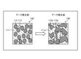
- FIG. 2 is a schematic diagram showing an example of the structure of the electrical contact material before and after arc generation according to the first embodiment
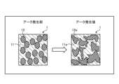
- FIG. 2 is a schematic diagram showing an example of the structure of the electrical contact material before and after arc generation according to the first embodiment
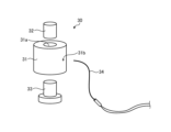
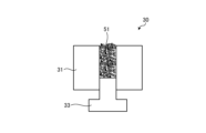
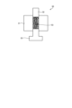
- FIG. 1 shows an example of the configuration of a graphite mold.
- FIG. 11 is a cross-sectional view showing an example of a procedure for filling a powder into a graphite mold in a manufacturing method of an electrical contact material according to a second embodiment.
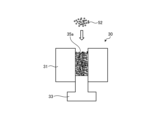
- FIG. 11 is a cross-sectional view showing an example of a procedure for filling a powder into a graphite mold in a manufacturing method of an electrical contact material according to a second embodiment.
- FIG. 11 is a cross-sectional view showing an example of a procedure for filling a powder into a graphite mold in a manufacturing method of an electrical contact material according to a second embodiment.
- FIG. 11 is a cross-sectional view showing an example of a procedure for filling a powder into a graphite mold in a manufacturing method of an electrical contact material according to a second embodiment.
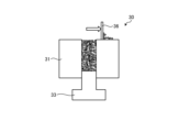
- FIG. 11 is a cross-sectional view showing an example of a procedure for filling a powder into a graphite mold in a manufacturing method of an electrical contact material according to a second embodiment.
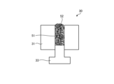
- FIG. 11 is a cross-sectional view showing an example of a procedure for filling a powder into a graphite mold in a manufacturing method of an electrical contact material according to a second embodiment.
- FIG. 11 is a cross-sectional view showing an example of a procedure for filling a powder into a graphite mold in a manufacturing method of an electrical contact material according to a second embodiment.
- FIG. 11 is a cross-sectional view showing an example of a procedure for filling a powder into a graphite mold in a manufacturing method of an electrical contact material according to a second embodiment.
- FIG. 11 is a perspective view showing an example of the configuration of a sintered body made of an electrical contact material according to a second embodiment;
- FIG. 13 is a diagram showing an example of an electrical contact made from an electrical contact material according to embodiment 2.
- FIG. SPS Spark Plasma Sinter
- FIG. 1 is a diagram showing an example of a procedure for manufacturing a fixed electrode
- FIG. 1 is a diagram showing an example of a procedure for manufacturing a fixed electrode
- Diagram showing the outline of the opening operation test device A diagram showing an image of electrical contacts opening when using an opening operation test device.
- a diagram showing an example of a waveform when measuring commutation time A diagram showing an example of a waveform when measuring a commutation time when the commutation time is short.
- FIG. 1 is a diagram showing an example of a method for measuring the contact resistance of an electrical contact;
- FIG. 1 is a diagram showing an example of a method for measuring the contact resistance of an electrical contact;
- FIG. 1 is a diagram showing an example of a method for measuring the contact resistance of an electrical contact
- FIG. 13 shows an S
- a diagram showing an example of a mold configuration. 11 is a cross-sectional view showing an example of a procedure for filling a powder into a die in a manufacturing method of an electrical contact material according to a third embodiment. 11 is a cross-sectional view showing an example of a procedure for filling a powder into a die in a manufacturing method of an electrical contact material according to a third embodiment.
- 11 is a cross-sectional view showing an example of a procedure for filling a powder into a die in a manufacturing method of an electrical contact material according to a third embodiment.
- 11 is a cross-sectional view showing an example of a procedure for filling a powder into a die in a manufacturing method of an electrical contact material according to a third embodiment.
- 11 is a cross-sectional view showing an example of a procedure for filling a powder into a die in a manufacturing method of an electrical contact material according to a third embodiment.
- 11 is a cross-sectional view showing an example of a procedure for filling a powder into a die in a manufacturing method of an electrical contact material according to a third embodiment.
- FIG. 11 is a cross-sectional view showing an example of a procedure for filling a powder into a die in a manufacturing method of an electrical contact material according to a third embodiment.
- 11 is a cross-sectional view showing an example of a procedure for filling a powder into a die in a manufacturing method of an electrical contact material according to a third embodiment.
- FIG. 1 is a diagram showing an example of the configuration of a sintered body after heat treatment.
- Embodiment 1 One of the electrical contact materials that constitutes electrical contacts used in air circuit breakers, switches, relays, and other power distribution control devices is Ag-SnO 2 (tin oxide).
- Ag-SnO 2 titanium oxide
- Ag-Cu copper
- Ag-Ni nickel
- Ag-SnO 2 has the advantage of being excellent in welding resistance and arc resistance, and is therefore often used in power distribution control device products with a rated current of 50A or more.
- SnO 2 has a higher decomposition temperature than CdO (cadmium oxide) and ZnO (zinc oxide), so it has the advantage of being excellent in wear resistance among oxide-based electrical contact materials, but it also has the disadvantage of being prone to remaining on the surface of electrical contacts and increasing the contact resistance of electrical contacts.
- the contact resistance of an electrical contact made of Ag-SnO 2 is likely to increase, it is desirable to divert the arc to the arc runner or other arc-extinguishing component side in as short a time as possible during interruption without causing the arc to stick on the electrical contact.
- the electrical contact material evaporates as metal vapor from the surface of the electrical contact to maintain the arc, but if the amount of evaporated metal vapor is large, the arc becomes easier to maintain, but the wear of the electrical contact increases.
- a method of reducing the wear of the electrical contact while maintaining the arc can be considered by adding a material that has excellent thermionic emission and a lower work function than the conductive component Ag and the arc -resistant component SnO 2.
- Compounds with a lower work function than pure metals such as Ag, Cu, and W (tungsten) that are usually used in electrical contacts include metal oxides, metal carbides, and metal borides.
- the work functions increase in the order of alkaline earth metal oxides such as BaO and SrO, metal borides such as LaB6 (lanthanum hexaboride), and metal carbides such as WC (tungsten carbide).
- a work function that is low compared to the work functions of the conductive and arc-proof components is referred to as a "low work function".
- a work function that is low compared to the work functions of the conductive and arc-proof components is referred to as a "low work function".
- FIG. 1 is a diagram showing an example of the structure of an electrical contact material made of Ag-SnO 2 containing a low work function component before and after arc generation.
- the electrical contact material 100 has a conductive component phase 111 that stably maintains an arc when an arc is generated, arc-resistant component particles 112 that suppress the consumption of the electrical contact material when an arc is generated, specifically, the consumption of the conductive component phase 111 when an arc is generated, and low-work function component particles 113 that commutate the arc when an arc is generated.
- An example of the conductive component phase 111 is Ag.
- An example of the arc-resistant component particles 112 is SnO 2.
- An example of the low-work function component particles 113 in the example of FIG. 1 is an alkaline earth metal oxide.
- the conductive component phase 111 is composed of a plurality of conductive component particles.
- arc-resistant component particles 112 and low work function component particles 113 are dispersed in conductive component phase 111.
- arc-resistant component particles 112 and low work function component particles 113 are physically dispersed.
- low work function component particles 113 are located farther away from each other than arc-resistant component particles 112. In this way, when arc-resistant component particles 112 and low work function component particles 113 are physically separated, there will be places on electrical contact material 100 where it is easy to divert the arc and places where it is difficult to divert the arc.
- the conductive component phase 111, the arc-resistant component particles 112, and the low work function component particles 113 also melt and resolidify to become the conductive component phase 111a, the arc-resistant component particles 112a, and the low work function component particles 113a, respectively. Since the arc-resistant component particles 112a and the low work function component particles 113a melt and resolidify, the surface shape, specifically the interface shape between the arc-resistant component particles 112a and the low work function component particles 113a and the conductive component phase 111a, becomes complex. Conventionally, the arc-resistant component particles 112a and the low work function component particles 113a remain physically separated even after an arc occurs.
- the arc-resistant component particles 112 are oxides
- the low work function component particles 113 are oxides
- a composite oxide composed of these oxides is dispersed in the conductive component phase 111.
- FIG. 2 is a diagram showing an example of the structure of the electrical contact material according to the first embodiment before and after the occurrence of an arc.
- the electrical contact material 1 has a conductive component phase 11 and a composite oxide particle 12 that suppresses the wear of the electrical contact when an arc occurs and commutates the arc.
- the composite oxide particle 12 includes an arc-resistant component element that is an element of an arc-resistant component and a low-work function component element that is an element of a low-work function component.
- An example of the conductive component phase 11 is Ag.
- the composite oxide particle 12 is a composite oxide particle in which an arc-resistant component oxide that is an oxide of an arc-resistant component element that suppresses the wear of the conductive component phase 11 when an arc occurs and a rare earth oxide that is a low-work function component having a work function lower than the work function of the conductive component phase 11 and the arc-resistant component oxide are mixed.
- An example of the arc-resistant component oxide is SnO2 .
- the arc-resistant component element is Sn.
- the rare earth oxide is an oxide of a rare earth element.
- the composite oxide is also called a mixed oxide.
- the composite oxide particles 12 are dispersed in the conductive component phase 11. In other words, unlike the case of FIG.
- the arc-resistant component oxide and the rare earth oxide of the low work function component are not separated, and a composite oxide is formed.
- the conductive component phase 11 and the composite oxide particles 12 constituting the surface of the electrical contact material 1 are melted and resolidified by the arc, and become the conductive component phase 11a and the composite oxide particles 12a, respectively.
- the conductive component phase 11a and the composite oxide particles 12a have the same composition and crystal structure as the conductive component phase 11 and the composite oxide particles 12, respectively.
- the composite oxide particles 12 have a particulate outer shape
- the composite oxide particles 12a have a complex surface shape because they are melted and resolidified.
- the composite oxide particles 12 are dispersed in the conductive component phase 11 before the arc is generated, but as shown in the right side of FIG. 2, the composite oxide particles 12a are maintained in a dispersed state in the conductive component phase 11a even after the arc is generated.
- the arc-resistant component oxide and the rare earth oxide of the low work function component are selected so that the composite oxide is maintained in a state in which the arc-resistant component oxide and the rare earth oxide of the low work function component are not separated even when the surface of the electrical contact material 1 is melted once by the arc and resolidified.
- the composite oxide particles 12, 12a having the low work function component element are uniformly distributed inside the electrical contact material 1, and the parts where the arc is easily diverted are uniformly present on the electrical contact material 1.
- the electrical contact material 1 unlike alkaline earth metal oxides, rare earth oxides, which are low work function components, are less likely to react with moisture and carbon dioxide in the air. This improves the arc commutation performance and reduces wear on the electrical contacts.
- the arc-resistant component oxide and the rare earth oxide of the low work function component constitute the composite oxide particles 12, but the electrical contact material 1 according to the first embodiment is not limited to this form.
- the arc-resistant component oxide particles and the rare earth oxide particles of the low work function component may be independently dispersed in the conductive component phase 11, and after an arc is generated, the arc-resistant component oxide particles and the rare earth oxide particles of the low work function component may constitute composite oxide particles 12a, and the composite oxide particles 12a may be dispersed in the conductive component phase 11.
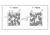
- FIG. 3 is a diagram showing an example of the structure of the electrical contact material before and after the generation of an arc according to the first embodiment.
- Ag powder which is a conductive component powder
- oxide powder are mixed and molded into a compact, which is heated to near the melting point of Ag and sintered.
- the melting points of the arc-resistant component oxide and the rare earth oxide of the low work function component used are both high, a composite oxide may not be formed at a sintering temperature near the melting point of Ag.
- the arc-resistant component oxide particle 13 which is the arc-resistant component oxide
- the rare earth oxide particle 14 which is the rare earth oxide of the low work function component
- the electrical contact of the present disclosure may be one in which such an electrical contact material 1A is used.
- Table 1 shows the atomic and ionic radii of the rare earth elements of Group III.
- Examples of rare earth elements of Group III include Sc (scandium), Y (yttrium), La, Ce (cerium), Pr (praseodymium), Nd (neodymium), Pm (promethium), Sm (samarium), Eu (europium), Gd (gadolinium), Tb (terbium), and Dy (dysprosium).
- Table 2 shows the atomic and ionic radii of arc-resistant component elements that are often used in arc-resistant component oxides. Examples of arc-resistant component elements include Zn (zinc), Sn, Ti (titanium), and Zr (zirconium).
- Table 3 shows the atomic and ionic radii of oxygen.
- perovskite compounds such as barium titanate BaTiO3.
- This compound contains one metal element A, one metal element B, and three elements X in a unit lattice, and is represented by the chemical formula ABX3 .
- the metal element A is Ba
- the metal element B is Ti
- the element X is O.
- the tolerance factor t is known as a condition for the perovskite structure to be established.
- the tolerance factor t is defined by the following formula (1).
- the tolerance factor t of perovskite compounds satisfies approximately 0.75 ⁇ t ⁇ 1.
- Perovskite compounds are a combination in which the ionic radius of metal element A is large and the ionic radius of metal element B is small.
- the ionic radius of Ba is 2.15 ⁇
- the ionic radius of Ti is 1.4 ⁇
- the ionic radius of O is 0.6 ⁇ .
- the metal element B is restricted to be a tetravalent positive ion.
- the metal element A is Ba2 + and the metal element B is Ti4 + .
- Ba is an alkaline earth metal of Group II, and Ti is a metal of Group IV.
- the metal element B is also a trivalent positive ion.
- the metal element A is a monovalent positive ion
- the metal element B is a pentavalent positive ion.
- metal element A is Sn and metal element B is La.
- Sn is a group IV element and is a tetravalent positive ion
- La is a group III element and is a trivalent positive ion, so even if the oxides are combined, they do not meet the conditions for forming a perovskite.
- Tables 1 and 2 the difference in the size of the ionic radius is a strong indicator of the ease with which oxides are combined.
- the electrical contact material 1, 1A contains, as main components, a composite oxide ABO3 composed of an oxide of a rare earth element which is a metal element A having a large ionic radius that satisfies the tolerance factor t > 0.8 , a metal element B which is an anti-arc component and has an ionic radius smaller than that of the metal element A, and Ag.
- a composite oxide ABO3 composed of an oxide of a rare earth element which is a metal element A having a large ionic radius that satisfies the tolerance factor t > 0.8 , a metal element B which is an anti-arc component and has an ionic radius smaller than that of the metal element A, and Ag.
- the tolerance factor t is calculated for a combination of a rare earth oxide of a low work function component and an oxide of an arc-proof component as shown below. Since the tolerance factor t satisfies 0.75 ⁇ t ⁇ 1 in the combinations of materials shown below, these combinations of materials are candidates for the composite oxide particles 12, 12a in the electrical contact materials 1, 1A.
- the electrical contact material 1, 1A according to the first embodiment includes Ag, which is the conductive component phase 11, and composite oxide particles 12 formed of an arc-resistant component oxide and a rare earth oxide of a low work function component.
- Ag which is the conductive component phase 11
- the reaction of the electrical contact material 1, 1A with moisture and carbon dioxide in the air can be suppressed.
- the arc-resistant component oxide and the rare earth oxide of the low work function component form a composite oxide and are uniformly distributed in the conductive component phase 11. Therefore, the composite oxide particles 12, 12a containing the low work function component are uniformly present at any point on the surface of the electrical contact material 1, 1A, making it easier to divert the arc.
- the rare earth oxide of the low work function component is an oxide of a rare earth element, which is metal element A
- the arc-resistant component oxide is an oxide of metal element B
- the tolerance factor expressed by formula (1) is 0.85 or more and less than 1.
- Embodiment 2 conditions for forming an electrical contact material 1 having composite oxide particles 12 selected from a combination of an arc-resistant component oxide containing Sn, which is the arc-resistant component element shown at the end of the first embodiment, and a rare earth oxide of a low-work-function component element containing La, Ce or Sm, which is a low-work-function component element, will be described.
- the conductive component powder constituting the conductive component phase 11 which is the raw material for the electrical contact material 1, the arc-resistant component oxide powder, and the rare earth oxide powder of the low work function component are weighed.
- Ag powder with an average particle size of 4 ⁇ m, SnO 2 powder with an average particle size of 1 ⁇ m, and rare earth oxide powder are prepared as raw materials for the electrical contact material 1.
- the rare earth oxide powder is La 2 O 3 powder with an average particle size of 1.5 ⁇ m, CeO 2 powder with an average particle size of 3 ⁇ m, or Sm 2 O 3 powder with an average particle size of 3 ⁇ m.
- Table 4 shows the volume ratio and mass ratio of the raw materials for the electrical contact material in Examples 1 to 4 and Comparative Examples 1 to 15. As shown in Table 4, each powder is weighed so that the amount of Ag added is constant at 75 vol% and the total value of the SnO 2 powder and the rare earth oxide powder is 25 vol%.
- the weighed conductive component powder, the anti-arc component oxide powder, and the low work function component rare earth oxide powder are mixed.
- a combination of Ag powder, SnO2 powder, and rare earth oxide powder, and a combination of only Ag powder and SnO2 powder are mixed by a dry mixer for 30 minutes each.
- FIG. 4 is a diagram showing an example of the configuration of a graphite mold.
- the graphite mold 30 has a die 31, an upper punch 32, and a lower punch 33, which are each separate.
- the die 31 is provided with a through hole 31a that contains the powder to be molded and into which the upper punch 32 and the lower punch 33 can be inserted.
- the diameter of the through hole 31a is ⁇ 15 mm.
- the die 31 is provided with a small hole 31b for a thermocouple that measures temperature.
- a thermocouple 34 is inserted into this small hole 31b.
- the thermocouple 34 is installed at a distance so that the tip of the thermocouple 34 does not come into direct contact with the powder.
- FIG. 5 to 11 are cross-sectional views showing an example of the procedure for filling the graphite mold with powder in the manufacturing method of the electrical contact material according to the second embodiment.
- a space 35 for filling the powder is formed by the die 31 of the graphite mold 30 and the lower punch 33 inserted into the through hole 31a provided in the die 31.
- the surface of the graphite mold 30 that the powder comes into contact with is sprayed with BN (boron nitride) to prevent the powder from sticking during the molding process.
- BN boron nitride
- the space 35 formed by the die 31 and the lower punch 33 of the graphite mold 30 is filled with a mixed powder 51 made by mixing Ag powder, SnO 2 powder, and rare earth oxide powder, or a mixed powder 51 made by mixing Ag powder and SnO 2 powder.
- a mixed powder 51 made by mixing Ag powder, SnO 2 powder, and rare earth oxide powder or a mixed powder 51 made by mixing Ag powder and SnO 2 powder.
- an amount that will result in a thickness of 2 mm when the electrical contact is completed is filled into the space 35.
- the excess mixed powder 51 present above the upper surface of the die 31 is leveled off by a leveling plate 36. This makes the surface of the mixed powder 51 filled in the space 35 flat.
- the lower punch 33 is lowered by a predetermined distance to form a gap 35a above the mixed powder 51 in the die 31.
- only Ag powder 52 is filled into the gap 35a formed in the die 31.
- the Ag powder 52 spread on the mixed powder 51 is weighed so that the thickness is 1/10 of the contact layer formed by sintering the mixed powder 51.
- the excess Ag powder 52 present above the upper surface of the die 31 is scraped off by the scraping plate 36. This makes the surface of the Ag powder 52 filled in the gap 35a flat.
- the upper punch 32 is placed on top of the Ag powder 52. When this is sintered, a two-layered compact 53 is formed.
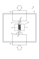
- FIG. 12 is a diagram showing an example of the sintering process in the SPS device.
- the SPS device 60 includes a vacuum chamber 61, an upper electrode 62, and a lower electrode 63.
- the graphite mold 30 is introduced into the vacuum chamber 61, and is sandwiched between the upper electrode 62 and the lower electrode 63.
- a pressure of about 3 kN is applied to the graphite mold 30 by the upper electrode 62 and the lower electrode 63, and the graphite mold 30 is temporarily fixed.
- the inside of the vacuum chamber 61 is evacuated by a vacuum pump (not shown), and the vacuum level is kept at 15 Pa or less.
- a rotary pump and a mechanical booster pump can be used as the vacuum pump.
- the pressure between the upper punch 32 and the lower punch 33 of the graphite mold 30 is increased to 7 kN.
- the pressure applied to the graphite mold 30 of ⁇ 15 mm becomes about 40 MPa.
- electricity is passed between the upper electrode 62 and the lower electrode 63 to heat the compact 53.
- the compact 53 is heated at a heating rate of 20°C/min, and when it reaches 850°C, it is held at 850°C for 10 minutes, and then the current is stopped to lower the temperature.
- the maximum voltage during current passing is about 2.5 V, and the current is about 500 A.
- the mixed powder 51 is only Ag powder and SnO2 powder, sintering is performed at 850°C.
- the mixed powder 51 is a mixture of Ag powder, SnO2 powder, and rare earth oxide powder, and the mixing ratio of SnO2 powder to rare earth oxide powder is 10:15 or 15:10
- Ag begins to melt at 850° C., so sintering is performed by lowering the temperature to 830° C. As a result, the compact 53 becomes a sintered body.
- FIG. 13 is a perspective view showing an example of the configuration of a sintered body made of the electrical contact material of embodiment 2.
- the sintered body 70 which is sintered powder, is made up of a contact layer 71 made of sintered mixed powder 51 and an Ag layer 72 made of sintered Ag powder 52.
- the upper side is the Ag layer 72 and the lower side is the contact layer 71, but FIG. 13 shows the sintered body 70 upside down.
- FIG. 14 is a diagram showing an example of an electrical contact made from the electrical contact material according to the second embodiment.
- the sintered body 70 is processed to obtain electrical contacts.
- two rectangular electrical contacts 80 are cut out from the completed sintered body 70 shown in FIG. 13 by machining using an electric discharge machine, as shown in FIG. 14.
- the electrical contacts 80 have a rectangular plate-shaped contact layer 81 formed by sintering the mixed powder 51, as in the sintered body 70, and a rectangular plate-shaped Ag layer 82 formed by sintering the Ag powder 52, which is disposed on one side of the contact layer 81.
- the electrical contacts 80 are cut out to have a size of 5.5 mm x 7 mm. Note that the scale of FIG. 13 is different from the scale of FIG. 14.
- Figures 15 and 16 are diagrams that show an example of the procedure of the manufacturing method of the fixed electrode.
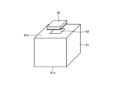
- Figure 15 is an oblique view
- Figure 16 is a cross-sectional view.
- a copper base 91 made of a rectangular block of copper is prepared.
- the copper base 91 is an electrode block that constitutes a part of the fixed electrode and the movable electrode in the circuit breaker.
- a screw hole (not shown) is machined in the first surface 91a of the copper base 91.
- the size of the copper base 91 is 14 mm x 14 mm x 10 mm.
- the diameter of the screw hole is M8.
- the electrical contact 80 carved out in Figure 14 is fixed to the second surface 91b opposite to the first surface 91a of the copper base 91, that is, the second surface 91b facing the first surface 91a.
- the brazing material 92 is placed on the second surface 91b of the copper pedestal 91, and the brazing material 92 is sandwiched between the rectangular electrical contact 80 and the copper pedestal 91 so that the Ag layer 82 side of the rectangular electrical contact 80 faces the brazing material 92.
- the rectangular electrical contact 80 is then brazed to the second surface 91b of the copper pedestal 91 by electrical heating.
- the brazing material 92 may be a silver brazing material such as BAg7, or a phosphorus copper brazing material such as BCuP5.
- the copper base 91 with the electrical contacts 80 brazed thereto is fixed to a square bar 93 constituting a part of the fixed electrode.
- the square bar 93 has a rectangular parallelepiped shape extending in one direction and is made of a conductive material such as copper.
- a screw hole 93a is machined at one end of the square bar 93 at a position where it is connected to the copper base 91.
- the diameter of the screw hole 93a is M8 in one example.
- the screw hole 93a penetrates the square bar 93.
- the copper base 91 and the square bar 93 are aligned, and a screw 94, which is a fixing member, is screwed from the screw hole 93a of the square bar 93 to the screw hole 91c of the copper base 91, thereby fixing the copper base 91 to the square bar 93. In this way, the fixed electrode is manufactured.
- the movable electrode is manufactured in the same way by fixing a copper base 91 to which an electrical contact 80 is brazed, using a screw 94 to a square bar that constitutes part of the movable electrode.
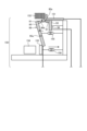
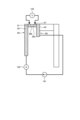
- FIG. 17 is a diagram showing an outline of the opening operation test device.
- the electrical contact 80 attached to the fixed electrode 98 is referred to as electrical contact 80a
- the electrical contact 80 attached to the movable electrode 99 is referred to as electrical contact 80b.
- the opening operation test device 150 is a simple test device that starts current flow with the electrical contact 80b and the electrical contact 80a in contact with each other, and cuts off the current by opening the electrical contact 80b with respect to the electrical contact 80a.
- the copper base 91 is fixed to a square bar 95, and a rotating shaft 95a is attached to the square bar 95.
- the electrical contact 80b of the movable electrode 99 is rotated on an arc around the rotating shaft 95a to open the contact.
- the electrical contact 80b and the electrical contact 80a are pressed with a constant force by a contact pressure spring 155, which is provided on the movable electrode 99 and is composed of a tension spring.
- An opening mechanism using an electromagnet 154 is attached to the opposite side of the movable electrode 99 from the electrical contact 80b with respect to the rotating shaft 95a.
- the opening mechanism has an electromagnet 154, an iron plate 153, and an opening spring 156.
- the opening spring 156 which is a tension spring, is attached to the opposite side of the iron plate 153 that is attracted to the electromagnet 154.
- the opening spring 156 With the iron plate 153 attracted by the electromagnet 154, the opening spring 156 is pulled to store energy, but because there is a small gap between the iron plate 153 and the movable electrode 99, the electrical contacts 80a and 80b remain pressed against each other by the contact pressure spring 155 even when the opening spring 156 is charged.
- An arc runner 151 for commutating the arc is installed near the fixed electrode 98, but the electrical contact 80a and the arc runner 151 are not in direct contact.
- iron plates arranged at equal intervals are made to play the role of so-called grid 152 in the circuit breaker arc extinguishing chamber. Wiring for current is attached to the movable electrode 99, the fixed electrode 98, and the arc runner 151.
- a DC high voltage power supply 164 is prepared for charging the variable capacitor 163, and the variable capacitor 163 and the variable reactor 161 are connected to the DC high voltage power supply 164.
- the opening operation test device 150 is designed to change the test current by adjusting the impedance by the combination of the variable capacitor 163 and the variable reactor 161.
- the set of the DC high voltage power supply 164 and the variable capacitor 163 corresponds to a capacitor bank power supply.
- the capacitor bank power supply is a power supply that uses a high-voltage DC power supply 164 to store an electric charge in a variable capacitor 163 and can pass a large current when discharging this charge.
- an LC resonant circuit is formed by the variable reactor 161, which is a coil, and the variable capacitor 163, and an alternating current is generated artificially.
- the artificially generated alternating current is used as the test current.
- the procedure for testing the opening operation test device 150 is to turn on the switches 167 and 168 on both ends of the DC high voltage power supply 164 to charge the variable capacitor 163.
- the switches 167 and 168 on both ends of the DC high voltage power supply 164 are turned off, and then the current start switch 162 on the variable reactor 161 side is turned on to start current flow to the opening operation test device 150.
- the current flow wiring is equipped with a fixed electrode side Rogowski coil current probe 165 for measuring the current of the entire system and an arc runner side Rogowski coil current probe 166 for measuring the arc current.
- the current in the wiring on the arc runner 151 side increases.
- the voltage between the fixed electrode 98 and the movable electrode 99 is measured by the high voltage measurement voltmeter 157.
- Figure 18 is a diagram showing an image of when the electrical contacts are opened in the opening operation test device.
- the iron plate 153 is attracted to the electromagnet 154 and charged in the opening spring 156, and the current to the electromagnet 154 is turned off when the electrical contacts 80a, 80b are opened, i.e., when the current start switch 162 is turned on.
- the iron plate 153 is attracted by the opening spring 156 and moves away from the electromagnet 154, pushing the end of the square bar 95 of the movable electrode 99 opposite the electrical contact 80b. Because the opening spring 156 is sufficiently stronger than the contact pressure spring 155, the electrical contacts 80a, 80b are opened.
- the timing when the current start switch 162 is turned on and the timing when the current to the electromagnet 154 is turned off can be freely adjusted, for example, by using a sequencer.
- the contact pressure or contact opening speed can be freely changed by replacing the contact pressure spring 155 or contact opening spring 156 with one with a different spring constant.
- the contact pressure spring 155 and contact opening spring 156 are selected so that the contact opening distance between the electrical contacts 80a and 80b is 30 mm, the contact pressure when the electrical contacts 80a and 80b are in contact is 10 N, and the contact opening speed is 3 m/s.
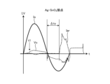
- FIG. 19 is a diagram showing an example of a waveform when measuring a commutation time.
- the horizontal axis indicates time t
- the vertical axis indicates a current value I or a voltage value V.
- FIG. 19 shows, as an example, a waveform when measuring a commutation time when the electrical contacts 80a, 80b are made of Ag-SnO 2.
- Graph Io shows the change in time of the current flowing through the entire system.
- the waveform of the current flowing through the entire system is a pseudo AC waveform created by a resonant circuit of the variable capacitor 163 and the variable reactor 161.
- the electrical contacts 80a, 80b When the electrical contacts 80a, 80b are in a closed state in which they are in contact, the current begins to flow, but the half-wave time is adjusted to 8.5 ms, which is almost the same as 8.33 ms, which is the half-wave time of 60 Hz AC.
- the arc runner 151 is placed at the same height as the electrical contact 80a so as to facilitate commutation, and is placed at a distance that does not contact the copper base 91, for example, 2 mm away.
- the grid 152 placed on the movable electrode 99 side is placed at a distance of 3 mm away from the track of the electrical contact 80b of the movable electrode 99.
- insulating tape is attached to the copper base 91 other than the electrical contacts 80a and 80b to prevent the arc from transferring to other parts.
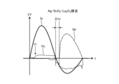
- FIG. 20 is a diagram showing an example of a waveform when the commutation time is short.
- the horizontal axis indicates time t
- the vertical axis indicates current value I or voltage value V.
- FIG. 20 shows, in one example, a waveform when the electrical contacts 80a, 80b are made of Ag-SnO 2 -La 2 O 3, that is, when composite oxide particles 12 made of SnO 2 and La 2 O 3 are dispersed in the conductive component phase 11 made of Ag.
- the current does not commute to the arc runner 151 in the first half wave, it commutes shortly after the second half wave begins.
- the commutation time ⁇ tc is shorter than that in FIG. 19.
- Figure 21 is a diagram showing a schematic diagram of an example of a method for measuring the contact resistance of electrical contacts.
- the resistance of the electrical contacts 80a, 80b can be measured using an opening operation test device 150.
- the capacitor bank power supply is removed and a DC constant current power supply 181 is connected.
- the electrical contacts 80a, 80b closed with a contact pressure of, for example, 10 N the resistance of the electrical contacts 80a, 80b is measured using the four-terminal method.
- a current of 10 A is passed between the fixed electrode 98 and the movable electrode 99 by a DC constant current power supply 181, the current flowing between the electrical contacts 80a and 80b is measured by an ammeter 182, and the voltage between the electrical contacts 80a and 80b is measured by a voltmeter 183 connected to the two copper pedestals 91, and the resistance of the electrical contacts 80a and 80b is calculated using the measured current and voltage.
- Table 5 shows the results of measuring the characteristics of the electrical contacts when an interruption test was performed for Examples 1 to 4 and Comparative Examples 1 to 15.
- the variable capacitor 163 and the variable reactor 161 were adjusted so that the root mean square value (RMS value) of the first half wave of the current flowing through the entire system was 5 kA, and the arc commutation time at each electrical contact 80a, 80b, the average wear of electrical contacts 80a, 80b, and the contact resistance of electrical contacts 80a, 80b before and after the test were summarized.
- the shape of electrical contacts 80a, 80b after the test was measured using a laser-type non-contact three-dimensional measuring device, and the average wear of the volume from when the electrical contacts 80a, 80b were new, i.e., before the test, was calculated.
- the average wear of the contacts is shown as a percentage of the average wear of the electrical contacts 80a, 80b before the test.
- the contact wear ratio to Comparative Example 1 shows how much electrical contacts 80a and 80b manufactured under other conditions wear compared to the amount of wear in Comparative Example 1, which does not contain rare earth oxide, a low work function component.
- the commutation time is shorter for the electrical contacts 80a, 80b of Examples 1 to 4 and Comparative Examples 2 and 3 containing La2O3 as the rare earth oxide of the low work function component, and the electrical contacts 80a, 80b of Comparative Example 9 containing CeO2 as the rare earth oxide of the low work function component than for Comparative Example 1.
- the electrical contacts 80a, 80b containing La2O3 as the rare earth oxide of the low work function component do not show as much improvement as the electrical contacts 80a, 80b containing La2O3 .
- the CeO 2 -based contacts 80a and 80b containing CeO 2 as a rare earth oxide of a low work function component have a slightly higher resistance value before the interruption test than Comparative Example 1.
- the electrical contacts 80a and 80b made of Ag-SnO 2 in Comparative Example 1 and the electrical contacts 80a and 80b made of Ag-SnO 2 -La 2 O 3 in Examples 1 to 4 and Comparative Examples 2 and 3 have almost the same resistance value, but the electrical contacts 80a and 80b made of Ag-SnO 2 -Sm 2 O 3 have a slightly higher resistance value than Comparative Example 1, and the electrical contacts 80a and 80b made of Ag-SnO 2 -CeO 2 have an even higher resistance value than Comparative Example 1.
- the electrical contacts 80a, 80b manufactured under the condition of adding 5 vol% or more and 20 vol% or less of La2O3 as a rare earth oxide with a low work function component show improvements in terms of the commutation time and wear of the electrical contacts 80a, 80b compared to the electrical contacts 80a, 80b made of Ag- SnO2 in Comparative Example 1.
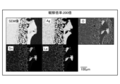
- the observation magnification here is 200 times.
- the elemental mapping is performed for the range shown in the SEM image. That is, FIG.
- FIG. 22 shows a cross-sectional SEM image of the Ag-SnO 2 -La 2 O 3 type electric contacts 80a and 80b, and an elemental mapping diagram of Ag, O, Sn, and La in this SEM image.
- FIG. 22 there are traces of melting and resolidification of the surfaces of the electric contacts 80a and 80b due to the arc at the time of opening.
- La, Sn, and O are detected at the same location. The results are the same even when the magnification is increased to 3,000 times.
- La, Sn, and O are precipitated in a mixed state, that is, in the state of a double oxide.
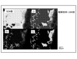
- the observation magnification here is 1,000 times.
- the element mapping is performed for the range shown in the SEM image.
- the element mapping of Ag is omitted. That is, FIG. 23 shows an SEM image of a cross section of an Ag-SnO 2 -CeO 2 based electrical contact 80a, 80b and an element mapping diagram of O, Sn, and Ce in this SEM image.
- Sn and Ce are present in different positions. Therefore, Sn, Ce, and O do not form a double oxide.
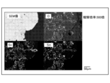
- the observation magnification here is 500 times.
- Element mapping is performed for the range shown in the SEM image.
- the element mapping result of Ag is omitted in FIG. 24. That is, FIG. 24 shows an SEM image of a cross section of an Ag-SnO 2 -Sm 2 O 3 based electrical contact 80a, 80b and an element mapping diagram of O, Sn, and Sm in this SEM image.
- Sn and Sm are present in different positions. Therefore, Sn, Sm, and O do not form a double oxide.
- the electrical contacts 80a, 80b according to the second embodiment are composite oxides formed of La2O3 , a rare earth oxide of a low work function component, and SnO2 , an anti-arc component oxide, and the content of the rare earth oxide in the electrical contacts 80a, 80b is 5 vol% or more and 20 vol% or less.
- a combination of the rare earth oxide of the low work function component and the anti-arc component oxide is selected so that the tolerance factor t of the electrical contacts 80a, 80b is greater than 0.845 and less than 1. This configuration has the effect of making it easier to uniformly commutate the arc on the surface compared to the conventional method while suppressing the reaction with moisture and carbon dioxide in the air.
- Embodiment 3 conditions for forming an electrical contact material 1 having composite oxide particles 12 selected from a combination of an arc-resistant component oxide containing Zn, which is the arc-resistant component element shown at the end of the first embodiment, and a rare earth oxide of a low work function component element containing La or Ce, which is a low work function component element, will be described.
- the conductive component powder constituting the conductive component phase 11 which is the raw material for the electrical contact material 1, the arc-resistant component oxide powder, and the rare earth oxide powder of the low work function component are weighed.
- Ag powder with an average particle size of 4 ⁇ m, ZnO powder with an average particle size of 1 ⁇ m, and rare earth oxide powder are prepared as raw materials for the electrical contact material 1.
- the rare earth oxide powder is La2O3 powder with an average particle size of 1.5 ⁇ m or CeO2 powder with an average particle size of 3 ⁇ m.
- Table 6 shows the volume ratio and mass ratio of the raw materials for the electrical contact material in Examples 5 to 7 and Comparative Examples 16 to 21. As shown in Table 6, each powder is weighed so that the amount of Ag added is constant at 80 vol% and the total value of the ZnO powder and the rare earth oxide powder is 20 vol%.
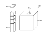
- FIG. 25 is a diagram showing an example of the configuration of a mold.
- the mold 200 has a die 201, an upper punch 202, and a lower punch 203, which are each separated.
- the die 201 is provided with a through hole 201a with a rectangular cross section that can accommodate the powder to be molded and can insert the upper punch 202 and the lower punch 203.
- the mold 200 is made of SKD (Steel Kogu Dice) 11 steel.
- SKD11 steel is an alloy tool steel material specified in G 4404:2015 of the Japanese Industrial Standards (JIS).
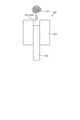
- 26 to 33 are cross-sectional views showing an example of the procedure for filling a mold with powder in the manufacturing method of an electrical contact material according to embodiment 3.
- a space 205 for filling the powder is formed by the die 201 of the mold 200 and the lower punch 203 inserted into the through hole 201a provided in the die 201.
- a thin layer of lubricant is applied to the surface of the mold 200 that the powder touches so that the powder does not stick during the molding operation.
- the space 205 formed by the die 201 and the lower punch 203 of the mold 200 is filled with a mixed powder 221 made by mixing Ag powder, ZnO powder, and rare earth oxide powder, or a mixed powder 221 made by mixing Ag powder and ZnO powder.
- the mixed powder 221 is filled in an amount such that the thickness of the contact layer formed by sintering the mixed powder 221 when the electrical contact is completed is 1.5 mm.
- the excess mixed powder 221 that is above the upper surface of the die 201 is scraped off by a scraping plate 226. This makes the surface of the mixed powder 221 that fills the space 205 flat.
- the lower punch 203 of the die 200 is lowered by a predetermined distance to form a gap 205a above the mixed powder 221 in the die 201.
- only Ag powder 222 is filled into the gap 205a formed in the die 201.
- the Ag powder 222 spread on the mixed powder 221 is weighed so that the thickness after sintering is 1/10 the thickness of the contact layer.
- the excess Ag powder 222 present above the upper surface of the die 201 is scraped off by a scraping plate 226. This makes the surface of the Ag powder 222 filled in the gap 205a flat.
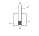
- the upper punch 202 is placed over the Ag powder 222.
- the die 200 is turned upside down and then molded at a predetermined molding pressure.
- the molding pressure is 640 MPa. This results in the formation of a two-layer molded body 223.
- the molded body 223 formed from the mixed powder 221 is sintered at a set sintering temperature to form a sintered body.
- the two-layered molded body 223 removed from the mold 200 is arranged on an alumina tray with the Ag layer facing down, and heat-treated in an atmospheric furnace, which is a heat treatment device, to sinter the two-layered molded body 223 to form a sintered body.
- sintering is performed at 940°C for two hours. After sintering, the temperature in the atmospheric furnace is sufficiently lowered to about 50°C, and the sintered body is removed.
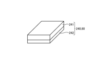
- Figure 34 is a diagram showing an example of the configuration of a sintered body after heat treatment. As shown in Figure 34, the removed sintered body 240 has a contact layer 241 and an Ag layer 242 formed at the same time.
- the following describes the procedure for manufacturing a circuit breaker using this sintered body 240 as the electrical contact 80 and conducting an evaluation test of the electrical contact 80.
- the sintered body 240 is used as the electrical contact 80 to manufacture a fixed electrode and a movable electrode that constitute the circuit breaker.
- a brazing material 92 is sandwiched between the second surface 91b of the copper pedestal 91 and the Ag layer 242 of the electrical contact 80, and then the electrical contact 80 is brazed to the copper pedestal 91 by resistance heating.
- the copper pedestal 91 to which the electrical contact 80 is brazed is fixed to the square bar 93 that constitutes a part of the fixed electrode, and the copper pedestal 91 is fixed to the square bar 95 that constitutes a part of the movable electrode, using screws 94.
- a fixed electrode 98 having a copper base 91 and a square bar 93 to which the electrical contact 80a is brazed, and a movable electrode 99 having a copper base 91 and a square bar 95 to which the electrical contact 80b is brazed are attached to the electrodes of an opening operation test device 150, and an electrical test is performed.
- the contact pressure spring 155 and opening spring 156 are selected so that the opening distance between the electrical contacts 80a and 80b is 30 mm, the contact pressure when the electrical contacts 80a and 80b come into contact is 7 N, and the opening speed is 3 m/s.
- Table 7 shows the measurement results of the characteristics of the electrical contacts when an interruption test was performed for Examples 5 to 7 and Comparative Examples 16 to 21.
- the variable capacitor 163 and variable reactor 161 were adjusted so that the effective value of the first half-wave of the current flowing through the entire system was 3 kA, and the arc commutation time at each electrical contact 80a, 80b, the average wear of electrical contacts 80a, 80b, and the contact resistance of electrical contacts 80a, 80b before and after the test were summarized when an interruption test was performed.
- the shape of electrical contacts 80a, 80b after the test was measured using a laser-type non-contact three-dimensional measuring device, and the average wear of the volume from when the electrical contacts 80a, 80b were new, i.e., before the test, was calculated.
- the average wear of the contacts is shown as a percentage of the average wear of the electrical contacts 80a, 80b before the test.
- the contact wear ratio to Comparative Example 16 shows the amount of wear of electrical contacts 80a and 80b manufactured under other conditions compared to the amount of wear of Comparative Example 16, which does not contain rare earth oxide, a low work function component.
- the electrical contacts 80a and 80b of Examples 5 to 7 and Comparative Example 17 containing La2O3 as the rare earth oxide of the low work function component, and the electrical contacts 80a and 80b of Comparative Example 20 containing CeO2 as the rare earth oxide of the low work function component, are shorter than the commutation time of Comparative Example 16.
- the electrical contacts 80a and 80b manufactured under the conditions of Examples 5 to 7 containing La2O3 as the rare earth oxide of the low work function component and having a rare earth oxide content in the range of 5 vol % to 15 vol% are less worn out than the electrical contacts 80a and 80b ... in contact resistance before and after the interruption test than the electrical contacts 80a and 80b of Comparative Example 16.
- the tolerance factor t of the low work function rare earth oxide and the anti-arc component oxide forming a double oxide is preferably greater than 0.845 and less than 1.
- the metal element A is a rare earth element other than Ce, and it is preferable that the tolerance factor t is greater than 0.845 and less than 1.
- the electrical contacts 80a, 80b according to the third embodiment contain the conductive component phase 11 formed of Ag, and the composite oxide particles 12 formed of La2O3 , which is a rare earth oxide having a low work function, and ZnO, which is an anti-arc component, and the content of the rare earth oxide in the electrical contact material 1 is 5 vol% or more and 15 vol% or less.
- This configuration has the effect of suppressing the reaction with moisture and carbon dioxide in the air, while making it easier to uniformly divert the arc on the surface compared to the conventional case.
- Embodiment 4 the conditions under which an electrical contact material 1 can be formed having composite oxide particles 12 selected from a combination of an arc-resistant component oxide containing Sn, which is the arc-resistant component element shown at the end of the first embodiment, and a rare earth oxide of a low work function component element containing Y, which is a low work function component element, will be described.
- the conductive component powder constituting conductive component phase 11 which is the raw material for electrical contact material 1A, the arc-resistant component oxide powder, and the rare earth oxide powder of the low work function component are weighed.
- Ag powder with an average particle size of 4 ⁇ m, SnO 2 powder with an average particle size of 1 ⁇ m, and Y 2 O 3 powder with an average particle size of 7 ⁇ m are prepared as raw materials for the electrical contact material 1A.
- the Y 2 O 3 powder is a rare earth oxide powder with a low work function component.
- Table 8 shows the volume ratio and mass ratio of the raw materials for the electrical contact material in Examples 8 to 10 and Comparative Examples 22 to 23. As shown in Table 8, each powder is weighed so that the amount of Ag added is constant at 78 vol% and the total value of the SnO 2 powder and the rare earth oxide powder is 22 vol%.
- the weighed conductive component powder, the anti-arc component oxide powder, and the low work function component rare earth oxide powder are mixed.
- a combination of Ag powder, SnO2 powder, and Y2O3 powder and a combination of only Ag powder and SnO2 powder are mixed by a dry mixer for 30 minutes each.
- the mixed powder is filled into a mold and molded at a set molding pressure.
- mixed powder 51 and Ag powder 52 are filled into a graphite mold 30 as shown in FIG. 4 in the procedure shown in FIG. 5 to FIG. 11 to form a molded body 53.
- the diameter ⁇ of the through hole 31a of the graphite mold 30 is 15 mm.
- the Ag powder 52 that forms the Ag layer 72 formed on the contact layer 71 formed by sintering the mixed powder 51 is weighed to be about 1/10 the thickness of the contact layer 71.
- the mixed powder 51 is sintered at a predetermined sintering temperature while applying pressure to form a sintered body 70.
- the graphite mold 30 filled with the mixed powder 51 and the Ag powder 52 is sintered by the SPS apparatus 60 shown in FIG. 12.
- the pressure between the upper punch 32 and the lower punch 33 of the graphite mold 30 is set to 7 kN, and the mold is heated at a temperature increase rate of 20°C/min.
- the mold reaches 850°C, the mold is held at 850°C for 10 minutes, and then the current is stopped to lower the temperature.
- the maximum voltage during current application is about 2.5 V, and the current is about 500 A.
- the mixed powder 51 is only Ag powder and SnO2 powder, sintering is performed at 850°C.
- the mixed powder 51 is Ag powder, SnO2 powder, and Y2O3 powder , and the mixing ratio of the SnO2 powder and the Y2O3 powder is 10:15 or 15:10, Ag begins to melt at 850° C., so sintering is performed at a temperature lowered to 830° C. As a result, the compact 53 becomes a sintered body 70.
- the graphite mold 30 is removed from the vacuum chamber 61, and the sintered body 70 is then removed from the graphite mold 30.
- the completed sintered body 70 is machined using an electric discharge machine to carve out two rectangular electrical contacts 80, as shown in FIG. 14.
- the electrical contacts 80 are carved out to have dimensions of 5.5 mm x 7 mm.
- the fixed electrode and movable electrode that make up the circuit breaker are manufactured using this electrical contact 80.
- a brazing material 92 is sandwiched between the second surface 91b of the copper pedestal 91 and the Ag layer 82 of the electrical contact 80, and then the electrical contact 80 is brazed to the copper pedestal 91 by resistance heating.
- the copper pedestal 91 to which the electrical contact 80 is brazed is fixed to a square bar 93 that forms part of the fixed electrode, and the copper pedestal 91 is fixed to a square bar 95 that forms part of the movable electrode, using screws 94.
- a fixed electrode 98 having a copper base 91 and a square bar 93 to which the electrical contact 80a is brazed, and a movable electrode 99 having a copper base 91 and a square bar 95 to which the electrical contact 80b is brazed are attached to the electrodes of an opening operation test device 150, and an electrical test is performed.
- the contact pressure spring 155 and the opening spring 156 are selected so that the opening distance between the electrical contacts 80a and 80b is 30 mm, the contact pressure when the electrical contacts 80a and 80b come into contact is 10 N, and the opening speed is 3 m/s.
- Table 9 shows the results of measuring the characteristics of the electrical contacts when the interruption test was performed for Examples 8 to 10 and Comparative Examples 22 to 23.
- Table 9 summarizes the commutation time of the arc at each of the electrical contacts 80a and 80b when the first interruption test and the second interruption test were performed, the average wear of the electrical contacts 80a and 80b, and the contact resistance of the electrical contacts 80a and 80b before and after the test.
- the variable capacitor 163 and the variable reactor 161 are adjusted so that the effective value of the first half wave of the current flowing through the entire system is 1 kA, and the first interruption test is performed.
- the variable capacitor 163 and the variable reactor 161 are readjusted so that the effective value of the first half wave of the current flowing through the entire system is 5 kA, and the second interruption test is performed.
- the wear and resistance of the electrical contacts 80a and 80b are measured after performing one interruption of 1 kA and one interruption of 5 kA each.
- the commutation time is not that short when a current of 1 kA is applied, but when a current of 5 kA is applied for the second time, the commutation time is clearly shorter than in Comparative Example 22, which does not contain rare earth oxide.
- the average wear of the contacts is also less than in Comparative Example 22, and the change in contact resistance is the same.
- the metal element A is a rare earth element other than Ce
- the tolerance factor t for the formation of a complex oxide between the rare earth oxide of the low work function component and the oxide of the arc-resistant component is preferably 0.85 or more and less than 1.
- the electrical contacts 80a and 80b according to the fourth embodiment are in a state in which the arc-resistant component oxide particles 13 and the low work function rare earth oxide particles 14 are dispersed in the conductive component phase 11. Then, when used as a circuit breaker, the arc-resistant component oxide particles 13 and the low work function rare earth oxide particles 14 present in the part that is exposed to the arc and melted and resolidified form a complex oxide. However, in order to form a complex oxide, the arc-resistant component element of the arc-resistant component oxide particles 13 and the rare earth element of the low work function rare earth oxide particles 14 must be a combination of elements that form a complex oxide.
- the electrical contacts 80a and 80b according to the fourth embodiment have a part that is melted by the arc where the complex oxide particles 12a containing the arc-resistant component element and the rare earth element are present, and a part that is not melted by the arc where the arc-resistant component oxide particles 13 and the low work function rare earth oxide particles 14 are dispersed.
- the arc-resistant component particles 112 and the low work function component particles 113 shown in FIG. 1 are dispersed in the conductive component phase 111
- the arc-resistant component particles 112a and the low work function component particles 113a do not form a complex oxide even after the arc occurs, and remain dispersed in the conductive component phase 111, as shown in the right figure. This is thought to be because the combination of the arc-resistant component elements constituting the arc-resistant component particles 112 and the alkaline earth elements constituting the low work function component particles 113 does not form a complex oxide.
- the combination of the arc-resistant component elements constituting the arc-resistant component oxide particles 13 and the rare earth elements constituting the low work function component rare earth oxide particles 14 forms a complex oxide. Therefore, in the part melted by the arc, the arc-resistant component oxide particles 13 and the low work function component rare earth oxide particles 14 melt and resolidify to form complex oxide particles 12a.
- the electrical contacts 80a and 80b according to the fourth embodiment include Ag, which is the conductive component phase 11, the arc-resistant component oxide particles 13, and the low-work function rare earth oxide particles 14, and the arc-resistant component elements constituting the arc-resistant component oxide particles 13 and the rare earth elements constituting the low-work function rare earth oxide particles 14 are made of materials that form a double oxide.
- the arc-resistant component oxide particles 13 and the low-work function rare earth oxide particles 14 are present separately in the conductive component phase 11, and when the surfaces of the electrical contacts 80a and 80b are melted and resolidified by an arc caused by interruption, the arc-resistant component oxide particles 13 and the low-work function rare earth oxide particles 14 form the double oxide particles 12a.
- the arc-resistant component oxide particles 13 and the low-work function rare earth oxide particles 14 are made of materials that form a double oxide at a temperature higher than the melting point of Ag.
- the rare earth oxide is Y2O3 , and the content of Y2O3 can be 5 vol% or more and 15 vol% or less.
- the commutation speed is not much different when the first arc occurs compared to when the rare earth oxide is not present, but when the second and subsequent arcs occur, the commutation speed can be improved and the wear rate of the electrical contacts 80a, 80b can be reduced. In other words, there is an effect that the ease of commutating the arc on the surface can be made more uniform than before while suppressing the reaction with moisture and carbon dioxide in the air.
Landscapes
- Chemical & Material Sciences (AREA)
- Engineering & Computer Science (AREA)
- Materials Engineering (AREA)
- Mechanical Engineering (AREA)
- Metallurgy (AREA)
- Organic Chemistry (AREA)
- Powder Metallurgy (AREA)
- Contacts (AREA)
Priority Applications (2)
| Application Number | Priority Date | Filing Date | Title |
|---|---|---|---|
| PCT/JP2023/028807 WO2025032703A1 (ja) | 2023-08-07 | 2023-08-07 | 電気接点材料およびその製造方法 |
| JP2025538981A JPWO2025032703A1 (cg-RX-API-DMAC7.html) | 2023-08-07 | 2023-08-07 |
Applications Claiming Priority (1)
| Application Number | Priority Date | Filing Date | Title |
|---|---|---|---|
| PCT/JP2023/028807 WO2025032703A1 (ja) | 2023-08-07 | 2023-08-07 | 電気接点材料およびその製造方法 |
Publications (1)
| Publication Number | Publication Date |
|---|---|
| WO2025032703A1 true WO2025032703A1 (ja) | 2025-02-13 |
Family
ID=94534211
Family Applications (1)
| Application Number | Title | Priority Date | Filing Date |
|---|---|---|---|
| PCT/JP2023/028807 Ceased WO2025032703A1 (ja) | 2023-08-07 | 2023-08-07 | 電気接点材料およびその製造方法 |
Country Status (2)
| Country | Link |
|---|---|
| JP (1) | JPWO2025032703A1 (cg-RX-API-DMAC7.html) |
| WO (1) | WO2025032703A1 (cg-RX-API-DMAC7.html) |
Citations (4)
| Publication number | Priority date | Publication date | Assignee | Title |
|---|---|---|---|---|
| JPS54100922A (en) * | 1978-01-26 | 1979-08-09 | Nippon Tungsten | Electrical contact material for breaker |
| JPS61272338A (ja) * | 1985-05-29 | 1986-12-02 | Sumitomo Electric Ind Ltd | 銀一酸化亜鉛系電気接点材料 |
| JP2015196903A (ja) * | 2014-03-31 | 2015-11-09 | 三菱電機株式会社 | Ag/SnO2電気接点用粉末、Ag/SnO2電気接点材料及びそれらの製造方法 |
| CN108929965A (zh) * | 2018-08-15 | 2018-12-04 | 宁波科扬贵金属合金科技有限公司 | 银氧化锡加重稀土触头材料的制造工艺 |
-
2023
- 2023-08-07 JP JP2025538981A patent/JPWO2025032703A1/ja active Pending
- 2023-08-07 WO PCT/JP2023/028807 patent/WO2025032703A1/ja not_active Ceased
Patent Citations (4)
| Publication number | Priority date | Publication date | Assignee | Title |
|---|---|---|---|---|
| JPS54100922A (en) * | 1978-01-26 | 1979-08-09 | Nippon Tungsten | Electrical contact material for breaker |
| JPS61272338A (ja) * | 1985-05-29 | 1986-12-02 | Sumitomo Electric Ind Ltd | 銀一酸化亜鉛系電気接点材料 |
| JP2015196903A (ja) * | 2014-03-31 | 2015-11-09 | 三菱電機株式会社 | Ag/SnO2電気接点用粉末、Ag/SnO2電気接点材料及びそれらの製造方法 |
| CN108929965A (zh) * | 2018-08-15 | 2018-12-04 | 宁波科扬贵金属合金科技有限公司 | 银氧化锡加重稀土触头材料的制造工艺 |
Also Published As
| Publication number | Publication date |
|---|---|
| JPWO2025032703A1 (cg-RX-API-DMAC7.html) | 2025-02-13 |
Similar Documents
| Publication | Publication Date | Title |
|---|---|---|
| Biyik | Effect of cubic and hexagonal boron nitride additions on the synthesis of Ag–SnO2 electrical contact material | |
| Zhang et al. | Arc erosion behavior of the Al2O3-Cu/(W, Cr) electrical contacts | |
| Li et al. | Effect of Ni addition on the arc-erosion behavior of AgTiB2 contact material | |
| JP6075423B1 (ja) | 真空遮断器 | |
| EP0488083B1 (en) | Contact material for a vacuum interrupter | |
| EP1528581B1 (en) | Electrical contact, method of manufacturing the same, electrode for vacuum interrupter, and vacuum circuit breaker | |
| EP3555898B1 (en) | Improved electrical contact alloy for vacuum contactors | |
| JP4455066B2 (ja) | 電気接点部材とその製法及びそれを用いた真空バルブ並びに真空遮断器 | |
| EP3062327A1 (en) | Electrical contact for vacuum valve and process for producing same | |
| EP0354997B1 (en) | Contact forming material for a vacuum interrupter | |
| JP6200669B2 (ja) | 電気接点材料 | |
| Biyik et al. | Effect of TiO2 content on the arc-erosion resistance of Ag/SnO2 electrical contact materials prepared via mechanical alloying-assisted powder metallurgy | |
| Qiu et al. | Arc erosion behavior of Ag-8 wt.% ZrO2 contact materials with CuO additions | |
| JP6050994B2 (ja) | 電気接点、電気接点の製造方法、電極、真空バルブ、真空開閉機器 | |
| KR20020079331A (ko) | 전기 접점 부재 및 그 생산 방법 | |
| EP2323148A1 (en) | Electric contact and vacuum interrupter using the same | |
| US11066731B2 (en) | Electric contact and vacuum interrupter using same | |
| JP5753244B2 (ja) | 接点材料およびそれを用いた遮断器 | |
| JP2013224484A (ja) | 電気接点材料およびその製造方法ならびに電気接点 | |
| JP4249356B2 (ja) | 電気接点材料 | |
| CN108149043A (zh) | 一种添加陶瓷相二硼化钛制备CuW合金的方法 | |
| US20060081560A1 (en) | Vacuum circuit breaker, vacuum interrupter, electric contact and method of manufacturing the same | |
| JP5142559B2 (ja) | 真空バルブ用接点材料及びその製造方法 | |
| JP2010061935A (ja) | 電気接点とその製造方法および電力開閉器 | |
| JP2002294384A (ja) | 電気接点材料 |
Legal Events
| Date | Code | Title | Description |
|---|---|---|---|
| 121 | Ep: the epo has been informed by wipo that ep was designated in this application |
Ref document number: 23948423 Country of ref document: EP Kind code of ref document: A1 |
|
| ENP | Entry into the national phase |
Ref document number: 2025538981 Country of ref document: JP Kind code of ref document: A |
|
| WWE | Wipo information: entry into national phase |
Ref document number: 2025538981 Country of ref document: JP |
|
| NENP | Non-entry into the national phase |
Ref country code: DE |
|
| 122 | Ep: pct application non-entry in european phase |
Ref document number: 23948423 Country of ref document: EP Kind code of ref document: A1 |