WO2025028178A1 - 半導体発光装置 - Google Patents
半導体発光装置 Download PDFInfo
- Publication number
- WO2025028178A1 WO2025028178A1 PCT/JP2024/024684 JP2024024684W WO2025028178A1 WO 2025028178 A1 WO2025028178 A1 WO 2025028178A1 JP 2024024684 W JP2024024684 W JP 2024024684W WO 2025028178 A1 WO2025028178 A1 WO 2025028178A1
- Authority
- WO
- WIPO (PCT)
- Prior art keywords
- electrode
- semiconductor light
- light emitting
- emitting element
- surface electrode
- Prior art date
- Legal status (The legal status is an assumption and is not a legal conclusion. Google has not performed a legal analysis and makes no representation as to the accuracy of the status listed.)
- Pending
Links
Images













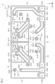
Classifications
-
- H—ELECTRICITY
- H01—ELECTRIC ELEMENTS
- H01S—DEVICES USING THE PROCESS OF LIGHT AMPLIFICATION BY STIMULATED EMISSION OF RADIATION [LASER] TO AMPLIFY OR GENERATE LIGHT; DEVICES USING STIMULATED EMISSION OF ELECTROMAGNETIC RADIATION IN WAVE RANGES OTHER THAN OPTICAL
- H01S5/00—Semiconductor lasers
- H01S5/02—Structural details or components not essential to laser action
- H01S5/022—Mountings; Housings
- H01S5/0239—Combinations of electrical or optical elements
-
- H—ELECTRICITY
- H01—ELECTRIC ELEMENTS
- H01S—DEVICES USING THE PROCESS OF LIGHT AMPLIFICATION BY STIMULATED EMISSION OF RADIATION [LASER] TO AMPLIFY OR GENERATE LIGHT; DEVICES USING STIMULATED EMISSION OF ELECTROMAGNETIC RADIATION IN WAVE RANGES OTHER THAN OPTICAL
- H01S5/00—Semiconductor lasers
- H01S5/02—Structural details or components not essential to laser action
- H01S5/024—Arrangements for thermal management
-
- H—ELECTRICITY
- H01—ELECTRIC ELEMENTS
- H01S—DEVICES USING THE PROCESS OF LIGHT AMPLIFICATION BY STIMULATED EMISSION OF RADIATION [LASER] TO AMPLIFY OR GENERATE LIGHT; DEVICES USING STIMULATED EMISSION OF ELECTROMAGNETIC RADIATION IN WAVE RANGES OTHER THAN OPTICAL
- H01S5/00—Semiconductor lasers
- H01S5/04—Processes or apparatus for excitation, e.g. pumping, e.g. by electron beams
- H01S5/042—Electrical excitation ; Circuits therefor
Definitions
- This disclosure relates to a semiconductor light-emitting device.
- a known type of semiconductor light-emitting device is a semiconductor laser device that includes a semiconductor light-emitting element as a laser light source (see, for example, Patent Document 1).
- the semiconductor laser device of Patent Document 1 includes multiple leads that are rod-shaped members. The multiple leads are used as terminals that are used when mounting the semiconductor laser device on electronic equipment, etc.
- a semiconductor light emitting device is a semiconductor light emitting device that includes a substrate having a substrate surface and a substrate back surface facing the opposite side to the substrate surface, a plurality of surface electrodes formed on the substrate surface, a plurality of back surface electrodes formed on the substrate back surface, electrically connected to the plurality of surface electrodes and constituting a mounting surface of the semiconductor light emitting device, a first semiconductor light emitting element and a second semiconductor light emitting element including an element surface electrode and an element back surface electrode, a first drive circuit that drives the first semiconductor light emitting element, and a second drive circuit that drives the second semiconductor light emitting element, and the element back surface electrode of the first semiconductor light emitting element, the element back surface electrode of the second semiconductor light emitting element, the first drive circuit, and the second drive circuit are mounted on the plurality of surface electrodes.
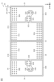
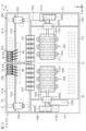
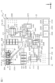
- FIG. 1 is a schematic plan view of a semiconductor light emitting device according to the first embodiment.
- FIG. 2 is a schematic plan view showing an enlarged portion of the semiconductor light emitting device of FIG.
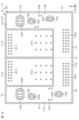
- FIG. 3 is a schematic rear view of the semiconductor light emitting device of FIG.
- FIG. 4 is a schematic cross-sectional view of the semiconductor light-emitting device taken along line F4-F4 in FIG.
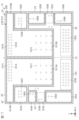
- FIG. 5 is a schematic plan view of a front-side intermediate electrode of the semiconductor light-emitting device of FIG.
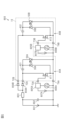
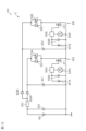
- FIG. 6 is a schematic circuit diagram of a light emitting system including the semiconductor light emitting device of the first embodiment.
- FIG. 7 is a schematic cross-sectional view of the semiconductor light emitting device of FIG. 4 mounted on a circuit board.
- FIG. 8 is a schematic cross-sectional view for explaining a current path flowing in a semiconductor light emitting device.
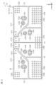
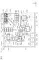
- FIG. 9 is a schematic plan view of a semiconductor light emitting device according to the second embodiment.
- FIG. 10 is a schematic plan view showing an enlarged portion of the semiconductor light emitting device of FIG.
- FIG. 11 is a schematic rear view of the semiconductor light emitting device of FIG. 12 is a schematic plan view of the front-side intermediate electrode of the semiconductor light-emitting device of FIG.
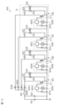
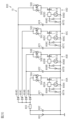
- FIG. 13 is a schematic circuit diagram of a light emitting system including the semiconductor light emitting device of the second embodiment.
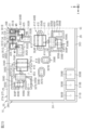
- FIG. 14 is a schematic plan view of a semiconductor light emitting device according to the third embodiment.
- FIG. 10 is a schematic plan view showing an enlarged portion of the semiconductor light emitting device of FIG.
- FIG. 15 is a schematic plan view showing an enlarged portion of the semiconductor light emitting device of FIG.
- FIG. 16 is a schematic plan view showing an enlarged view of another part of the semiconductor light emitting device of FIG. 17 is a schematic rear view of the semiconductor light emitting device of FIG. 18 is a schematic plan view of the front surface side intermediate electrode of the semiconductor light emitting device of FIG.
- FIG. 19 is a schematic circuit diagram of a light emitting system including the semiconductor light emitting device of the third embodiment.
- FIG. 20 is a schematic plan view of the semiconductor light emitting device according to the fourth embodiment.
- FIG. 23 is a schematic rear view of the semiconductor light emitting device of FIG. 24 is a schematic plan view of a front surface side intermediate electrode of the semiconductor light emitting device of FIG. 25 is a schematic plan view of a back surface side intermediate electrode of the semiconductor light emitting device of FIG.
- FIG. 26 is a schematic circuit diagram of a light emitting system including the semiconductor light emitting device of the fourth embodiment.
- FIG. 27 is a schematic plan view of a semiconductor light emitting device according to the fifth embodiment.
- FIG. 28 is a schematic plan view showing an enlarged portion of the semiconductor light emitting device of FIG. 29 is a schematic plan view showing an enlarged view of another part of the semiconductor light emitting device of FIG. 30 is a schematic rear view of the semiconductor light emitting device of FIG. 31 is a schematic plan view of a front surface side intermediate electrode of the semiconductor light emitting device of FIG. 32 is a schematic plan view of a rear intermediate electrode of the semiconductor light emitting device of FIG.
- FIG. 1 shows a schematic planar structure of the semiconductor light emitting device 10.
- FIG. 2 shows a schematic planar structure of an enlarged half of the substrate 20 near the first substrate side surface 23 in the semiconductor light emitting device 10 shown in FIG. 1, which will be described later.
- FIG. 3 shows a schematic rear structure of the semiconductor light emitting device 10.
- FIG. 4 shows a schematic cross-sectional structure of the semiconductor light emitting device 10 cut along the line F4-F4 in FIG. 1.
- FIG. 5 shows a schematic planar structure of the front surface side intermediate electrode 28C in the semiconductor light emitting device 10, which will be described later.
- FIG. 6 shows a schematic circuit configuration of a light emitting system 800 including the semiconductor light emitting device 10.
- FIG. 7 shows a schematic cross-sectional structure of the semiconductor light emitting device 10 mounted on a circuit board 900.
- FIG. 8 shows an explanatory diagram for explaining the flow of current flowing through the semiconductor light emitting device 10.
- FIG. 4 FIG. 7, and FIG. 8, hatching lines of some members are omitted in order to facilitate understanding of the drawings.
- the term "planar view” used in this disclosure refers to viewing the semiconductor light emitting device 10 in the Z direction of the mutually orthogonal XYZ axes shown in FIG. 1.
- the "X direction” is an example of the "second direction”
- the "Y direction” is an example of the "first direction”.
- the semiconductor light emitting device 10 includes a substrate 20, and a first semiconductor light emitting element 30A, a second semiconductor light emitting element 30B, a first drive circuit 40A, and a second drive circuit 40B arranged on the substrate 20.
- the first semiconductor light emitting element 30A, the second semiconductor light emitting element 30B, the first drive circuit 40A, and the second drive circuit 40B are arranged on the substrate 20 at a distance from each other.
- the substrate 20 is a component that supports the first semiconductor light-emitting element 30A, the second semiconductor light-emitting element 30B, the first drive circuit 40A, and the second drive circuit 40B.
- the substrate 20 is formed in a rectangular flat plate shape with the thickness direction being the Z direction.
- plane view is synonymous with "viewed from the thickness direction of the substrate.”
- the substrate 20 is formed in a rectangular shape with its longitudinal direction in the X direction and its transverse direction in the Y direction in a plan view.
- the substrate 20 has a substrate surface 21, a substrate back surface 22 (see FIG. 4) facing the opposite side to the substrate surface 21 in the Z direction, and first to fourth substrate side surfaces 23 to 26 connecting the substrate surface 21 and the substrate back surface 22.
- the first substrate side surface 23 and the second substrate side surface 24 form both end surfaces of the substrate 20 in the X direction
- the third substrate side surface 25 and the fourth substrate side surface 26 form both end surfaces of the substrate 20 in the Y direction.
- the shape of the substrate 20 in a plan view can be changed as desired.
- the substrate 20 is a four-layer substrate. That is, the substrate 20 includes a plurality of base materials 27, and a plurality of front electrodes 28A, a plurality of rear electrodes 28B, a plurality of front intermediate electrodes 28C, and a plurality of rear intermediate electrodes 28D provided on the base materials 27.
- Each of the front electrodes 28A, each of the rear electrodes 28B, each of the front intermediate electrodes 28C, and each of the rear intermediate electrodes 28D is formed of a material including one or more appropriately selected from the following: Ti (titanium), TiN (titanium nitride), Au (gold), Ag (silver), Cu (copper), Al (aluminum), and W (tungsten).
- the base material 27 is formed of, for example, an insulating material.
- the insulating material may be formed of, for example, a material containing epoxy resin.
- the base material 27 may be formed of glass epoxy resin.
- the insulating material may also be formed of, for example, a material containing ceramic. Examples of materials containing ceramic include aluminum nitride (AlN) and alumina (Al 2 O 3 ).
- AlN aluminum nitride
- Al 2 O 3 alumina
- the substrate front surface 21, the substrate back surface 22, and the first to fourth substrate side surfaces 23 to 26 refer to the substrate front surface, substrate back surface, and first to fourth substrate side surfaces of the base material 27.
- the base material 27 includes three substrates, namely, a front surface substrate 27A, a back surface substrate 27B, and an intermediate substrate 27C.
- the substrate front surface 21 of the substrate 20 is constituted by the substrate surface of the front surface substrate 27A.
- the rear surface 22 of the substrate 20 is formed by the rear surface of the rear substrate 27B.
- the first to fourth substrate side surfaces of the substrate 20 are formed by the first to fourth substrate side surfaces of the front substrate 27A, the rear substrate 27B, and the intermediate substrate 27C.
- the first to fourth substrate side surfaces 23 to 26 (FIG.
- FIG. 4 shows the third substrate side surface 25 and the fourth substrate side surface 26), the ends of the front intermediate electrode 28C and the rear intermediate electrode 28D are covered by the substrates 27A, 27B, and 27C.
- the substrates 27A, 27B, and 27C and the portions covering the ends of the front intermediate electrode 28C and the rear intermediate electrode 28D are shown by solid lines.
- the interfaces of the substrates 27A, 27B, and 27C may not be clear.
- the detailed configurations of the front electrode 28A, the rear electrode 28B, and the front intermediate electrode 28C will be described below.
- the configuration of the rear surface side intermediate electrode 28D is the same as that of the front surface side intermediate electrode 28C, and therefore a detailed description thereof will be omitted.
- the plurality of surface electrodes 28A are formed on the substrate surface 21.
- the plurality of surface electrodes 28A include first surface electrodes 61A, 61B, second surface electrodes 62A, 62B, third surface electrodes 63A, 63B, fourth surface electrodes 64A, 64B, and fifth surface electrodes 65A, 65B that are arranged spaced apart from one another.
- the first surface electrode 61A, the second surface electrode 62A, the third surface electrode 63A, the fourth surface electrode 64A, and the fifth surface electrode 65A are arranged closer to the first substrate side surface 23 than a virtual center line VC that extends along the Y direction at the center of the X direction of the substrate surface 21.
- the first surface electrode 61B, the second surface electrode 62B, the third surface electrode 63B, the fourth surface electrode 64B, and the fifth surface electrode 65B are arranged closer to the second substrate side surface 24 than the virtual center line VC.
- the first surface electrode 61A, the second surface electrode 62A, the third surface electrode 63A, the fourth surface electrode 64A, and the fifth surface electrode 65A are in a line-symmetrical relationship with the first surface electrode 61B, the second surface electrode 62B, the third surface electrode 63B, the fourth surface electrode 64B, and the fifth surface electrode 65B with respect to the virtual center line VC.
- first surface electrode 61A the first surface electrode 61A, the second surface electrode 62A, the third surface electrode 63A, the fourth surface electrode 64A, and the fifth surface electrode 65A, and will omit a detailed description of the first surface electrode 61B, the second surface electrode 62B, the third surface electrode 63B, the fourth surface electrode 64B, and the fifth surface electrode 65B.
- the first surface electrode 61A and the fifth surface electrode 65A are disposed in a distributed manner at both ends of the substrate surface 21 in the Y direction.
- the first surface electrode 61A is disposed at the end of the substrate surface 21 closer to the third substrate side surface 25.
- the fifth surface electrode 65A is disposed at the end of the substrate surface 21 closer to the fourth substrate side surface 26.
- Both the first surface electrode 61A and the fifth surface electrode 65A are disposed at positions adjacent to the imaginary center line VC in the X direction.
- Both the first surface electrode 61A and the fifth surface electrode 65A are formed in a rectangular shape with the X direction being the long side and the Y direction being the short side in a plan view.
- the X direction dimension of the first surface electrode 61A and the X direction dimension of the fifth surface electrode 65A are equal to each other.
- the Y direction dimension of the fifth surface electrode 65A is larger than the Y direction dimension of the first surface electrode 61A.
- the second surface electrode 62A is disposed between the first surface electrode 61A and the fifth surface electrode 65A in the Y direction.
- the second surface electrode 62A is formed in a substantially L-shape in a planar view.
- the second surface electrode 62A is disposed closer to the imaginary center line VC than the third surface electrode 63A and the fourth surface electrode 64A.
- the second surface electrode 62A includes a narrow portion 62AA and a wide portion 62AB.
- the narrow portion 62AA is a portion of the second surface electrode 62A that has a smaller dimension in the X direction.
- the wide portion 62AB is a portion of the second surface electrode 62A that has a larger dimension in the X direction.
- the narrow portion 62AA and the wide portion 62AB are aligned in the Y direction.
- the narrow portion 62AA and the wide portion 62AB are integrated.
- the narrow portion 62AA is disposed adjacent to the first surface electrode 61A in the Y direction.
- the wide portion 62AB is disposed at a position adjacent to the fifth surface electrode 65A in the Y direction.
- the wide portion 62AB protrudes toward the first substrate side surface 23 relative to the narrow portion 62AA.
- the X-direction dimension of the narrow portion 62AA is smaller than the X-direction dimension of the first surface electrode 61A.
- the X-direction dimension of the wide portion 62AB is larger than the X-direction dimension of the fifth surface electrode 65A.
- the third surface electrode 63A is formed to surround the wide portion 62AB of the second surface electrode 62A from the first substrate side surface 23 side and the third substrate side surface 25 side.
- the third surface electrode 63A includes a first opposing portion, a second opposing portion, and a connecting portion. The first opposing portion and the second opposing portion form both ends in the direction in which the third surface electrode 63A extends.
- the first opposing portion is located closer to the third substrate side surface 25 than the wide portion 62AB, and faces the narrow portion 62AA in the X direction.
- the first opposing portion is disposed in a position adjacent to the narrow portion 62AA in the X direction.
- the second opposing portion is located closer to the first substrate side surface 23 than the wide portion 62AB, and adjacent to the wide portion 62AB in the X direction.
- the connecting portion connects the first opposing portion and the second opposing portion.
- the connecting portion extends obliquely toward the first substrate side surface 23 as it moves from the first opposing portion to the second opposing portion.
- the third surface electrode 63A is composed of wiring having a constant width.
- the fourth surface electrode 64A includes a portion formed from the third substrate side surface 25 to the fourth substrate side surface 26 at the end of the substrate surface 21 closer to the first substrate side surface 23.
- the fourth surface electrode 64A includes a recessed portion 64AA that accommodates a part of the first surface electrode 61A, and a recessed portion 64AB that accommodates a part of the third surface electrode 63A and a part of the wide portion 62AB of the second surface electrode 62A.
- the end of the fourth surface electrode 64A closer to the fourth substrate side surface 26 in the Y direction is formed to be adjacent to the fifth surface electrode 65A in the X direction and adjacent to the wide portion 62AB in the Y direction.
- the fourth surface electrode 64A includes a wiring portion 64AC formed to be adjacent to the narrow portion 62AA in the X direction.
- the wiring portion 64AC constitutes a part of the recessed portion 64AA.
- the wiring portion 64AC is disposed between the first surface electrode 61A and the third surface electrode 63A in the Y direction.
- the multiple back electrodes 28B are formed on the substrate back surface 22.
- the multiple back electrodes 28B are electrically connected to the multiple front electrodes 28A and constitute the mounting surface of the semiconductor light emitting device 10.
- the multiple back electrodes 28B include first back electrodes 71A, 71B, second back electrodes 72A, 72B, third back electrodes 73A, 73B, and fourth back electrodes 74A, 74B that are arranged apart from each other.
- the second back electrodes 72A, 72B, third back electrodes 73A, 73B, and fourth back electrodes 74A, 74B constitute external electrode terminals that are electrically connected to the circuit board when the semiconductor light emitting device 10 is mounted on the circuit board.
- the first back electrodes 71A, 71B are heat dissipation electrodes for dissipating heat to the outside of the semiconductor light emitting device 10.
- the first back surface electrode 71A, the second back surface electrode 72A, the third back surface electrode 73A, and the fourth back surface electrode 74A are arranged closer to the first substrate side surface 23 than the virtual center line VC.
- the first back surface electrode 71B, the second back surface electrode 72B, the third back surface electrode 73B, and the fourth back surface electrode 74B are arranged closer to the second substrate side surface 24 than the virtual center line VC.
- the first back surface electrode 71A, the second back surface electrode 72A, the third back surface electrode 73A, and the fourth back surface electrode 74A are in a linear symmetrical relationship with the first back surface electrode 71B, the second back surface electrode 72B, the third back surface electrode 73B, and the fourth back surface electrode 74B with respect to the virtual center line VC.
- the following will describe in detail the first back surface electrode 71A, the second back surface electrode 72A, the third back surface electrode 73A, and the fourth back surface electrode 74A, and will omit a detailed description of the first back surface electrode 71B, the second back surface electrode 72B, the third back surface electrode 73B, and the fourth back surface electrode 74B.
- the first back surface electrode 71A is a back surface electrode electrically connected to the first surface electrode 61A and the fifth surface electrode 65A (both see FIG. 1). In other words, the first surface electrode 61A and the fifth surface electrode 65A are electrically connected via the first back surface electrode 71A.
- the first back surface electrode 71A is disposed at a position adjacent to the imaginary center line VC in the X direction.
- the first back surface electrode 71A is formed from the third substrate side surface 25 to the fourth substrate side surface 26 in the Y direction. Therefore, the first back surface electrode 71A includes a portion that overlaps with the first surface electrode 61A in a planar view and a portion that overlaps with the fifth surface electrode 65A in a planar view.
- the second to fourth back electrodes 72A to 74A are arranged closer to the first substrate side surface 23 than the first back electrode 71A.
- the second back electrode 72A and the third back electrode 73A are arranged closer to the fourth substrate side surface 26 than the center in the Y direction of the substrate back surface 22.
- the second back electrode 72A and the third back electrode 73A are arranged side by side in the X direction.
- the second back electrode 72A is arranged closer to the first back electrode 71A than the third back electrode 73A.
- the fourth back electrode 74A is formed to surround the second back electrode 72A and the third back electrode 73A from the first substrate side surface 23 and the third substrate side surface 25.
- the second back surface electrode 72A is an electrode that is electrically connected to the second surface electrode 62A (see FIG. 1).
- the second back surface electrode 72A is formed in a band shape extending in the Y direction.
- the second back surface electrode 72A includes a portion that overlaps with the wide portion 62AB (see FIG. 1) of the second surface electrode 62A in a plan view.
- the third back surface electrode 73A is an electrode electrically connected to the third surface electrode 63A (see FIG. 1).
- the third back surface electrode 73A is formed in a band shape extending in the Y direction.
- the dimension of the third back surface electrode 73A in the Y direction is smaller than the dimension of the second back surface electrode 72A in the Y direction.
- the third back surface electrode 73A includes a portion that overlaps with the second opposing portion of the third surface electrode 63A in a plan view.
- the fourth back surface electrode 74A is an electrode electrically connected to the fourth surface electrode 64A (see FIG. 1).
- the fourth back surface electrode 74A includes a first portion 74AA that is square in plan view and is formed closer to the third substrate side surface 25 than the center in the Y direction of the substrate back surface 22, and a strip-shaped second portion 74AB that extends in the Y direction from the first portion 74AA toward the fourth substrate side surface 26.
- the second portion 74AB is disposed closer to the first substrate side surface 23 than the third back surface electrode 73A.
- the fourth back surface electrode 74A includes a portion that overlaps with the fourth surface electrode 64A in plan view.
- the area of the first back surface electrode 71A is larger than each of the areas of the second to fourth back surface electrodes 72A to 74A. In one example, the area of the first back surface electrode 71A is larger than the sum of the areas of the second to fourth back surface electrodes 72A to 74A.
- the plurality of front-side intermediate electrodes 28C are formed in the substrate 27. More specifically, the plurality of front-side intermediate electrodes 28C are sandwiched between the front-side substrate 27A and the intermediate substrate 27C (see Fig. 4 for both).
- the plurality of front-side intermediate electrodes 28C include first intermediate electrodes 81A, 81B, second intermediate electrodes 82A, 82B, third intermediate electrodes 83A, 83B, and fourth intermediate electrodes 84A, 84B that are arranged apart from one another.
- the first intermediate electrode 81A, the second intermediate electrode 82A, the third intermediate electrode 83A, and the fourth intermediate electrode 84A are arranged closer to the first substrate side surface 23 than the virtual center line VC.
- the first intermediate electrode 81B, the second intermediate electrode 82B, the third intermediate electrode 83B, and the fourth intermediate electrode 84B are arranged closer to the second substrate side surface 24 than the virtual center line VC.
- the first intermediate electrode 81A, the second intermediate electrode 82A, the third intermediate electrode 83A, and the fourth intermediate electrode 84A are in a linear symmetrical relationship with the first intermediate electrode 81B, the second intermediate electrode 82B, the third intermediate electrode 83B, and the fourth intermediate electrode 84B with respect to the virtual center line VC.
- first intermediate electrode 81A the first intermediate electrode 81A, the second intermediate electrode 82A, the third intermediate electrode 83A, and the fourth intermediate electrode 84A, and will omit a detailed description of the first intermediate electrode 81B, the second intermediate electrode 82B, the third intermediate electrode 83B, and the fourth intermediate electrode 84B.
- the first intermediate electrode 81A is a back surface electrode that electrically connects the first surface electrode 61A and the fifth surface electrode 65A (see FIG. 1 for both). That is, the first surface electrode 61A and the fifth surface electrode 65A are electrically connected via the first intermediate electrode 81A.
- the first intermediate electrode 81A is also electrically connected to the first back surface electrode 71A (see FIG. 3).
- the first intermediate electrode 81A is disposed at a position adjacent to the imaginary center line VC in the X direction.
- the first intermediate electrode 81A is formed from the third substrate side surface 25 to the fourth substrate side surface 26 in the Y direction. Therefore, the first intermediate electrode 81A includes a portion that overlaps with the first surface electrode 61A in a plan view and a portion that overlaps with the fifth surface electrode 65A in a plan view.
- the second intermediate electrode 82A is an electrode that electrically connects the second surface electrode 62A (see FIG. 1) and the second back surface electrode 72A (see FIG. 3).
- the third intermediate electrode 83A is an electrode that electrically connects the third surface electrode 63A (see FIG. 1) and the third back surface electrode 73A (see FIG. 3).
- the second intermediate electrode 82A and the third intermediate electrode 83A are arranged in the electrode accommodating portion of the fourth intermediate electrode 84A.
- the electrode accommodating portion is a generally concave shape that extends in the X direction and opens toward the imaginary center line VC.
- the second intermediate electrode 82A and the third intermediate electrode 83A are arranged side by side in the X direction.
- the second intermediate electrode 82A is arranged closer to the first intermediate electrode 81A than the third intermediate electrode 83A.
- the second intermediate electrode 82A is formed in a generally right-angled trapezoid shape.
- the third intermediate electrode 83A is formed in an elliptical shape with the Y direction as the longitudinal direction and the X direction as the transverse direction.
- the second intermediate electrode 82A includes a portion that overlaps with both the wide portion 62AB (see FIG. 1) of the second surface electrode 62A and the second back surface electrode 72A in a plan view.
- the third intermediate electrode 83A includes a portion that overlaps with both the second opposing portion (see FIG. 1) of the third surface electrode 63A and the third back surface electrode 73A (see FIG. 3) in a plan view.
- the fourth intermediate electrode 84A is an electrode that electrically connects the fourth surface electrode 64A (see FIG. 1) and the fourth back surface electrode 74A (see FIG. 3).
- the fourth intermediate electrode 84A is formed over most of the portion of the substrate surface of the intermediate substrate 27C that is closer to the first substrate side surface 23 than the first intermediate electrode 81A.
- the fourth intermediate electrode 84A includes a portion that overlaps with both the fourth surface electrode 64A (see FIG. 1) and the fourth back surface electrode 74A (see FIG. 3).
- the substrate 20 includes first vias 91A, 91B, second vias 92A, 92B, third vias 93A, 93B, fourth vias 94A, 94B, and fifth vias 95A, 95B.
- the first vias 91A, 91B, second vias 92A, 92B, third vias 93A, 93B, fourth vias 94A, 94B, and fifth vias 95A, 95B are provided to penetrate the respective base materials 27A, 27B, 27C, the front-side intermediate electrode 28C, and the back-side intermediate electrode 28D in the Z direction.
- the first vias 91A, 91B, second vias 92A, 92B, third vias 93A, 93B, fourth vias 94A, 94B, and fifth vias 95A, 95B may be provided to penetrate the front-side electrode 28A and the back-side electrode 28B in the Z direction.
- the first vias 91A, 91B, the second vias 92A, 92B, the third vias 93A, 93B, the fourth vias 94A, 94B, and the fifth vias 95A, 95B are formed from a material including one or more appropriately selected from the group consisting of Ti, TiN, Au, Ag, Cu, Al, and W.
- the first via 91A, the second via 92A, the third via 93A, the fourth via 94A, and the fifth via 95A are arranged closer to the first substrate side surface 23 than the imaginary center line VC.
- the first via 91B, the second via 92B, the third via 93B, the fourth via 94B, and the fifth via 95A are arranged closer to the second substrate side surface 24 than the imaginary center line VC.
- the first to fifth vias 91A to 95A and the first to fifth vias 91B to 95B are in a line-symmetrical relationship with respect to the imaginary center line VC. For this reason, the first to fifth vias 91A to 95A will be described in detail below, and a detailed description of the first to fifth vias 91B to 95B will be omitted.
- first to fifth vias 91A to 95A There are multiple first to fifth vias 91A to 95A. There are the same number of first vias 91A and fifth vias 95A, and the number of each of the second to fourth vias 92A to 94A is less than the number of first vias 91A. The number of fourth vias 94A is greater than the number of each of the second vias 92A and third vias 93A. The number of third vias 93A is less than the number of second vias 92A.
- the first via 91A is electrically connected to the first surface electrode 61A, the first intermediate electrode 81A of the surface-side intermediate electrode 28C, the first intermediate electrode 81A of the back-side intermediate electrode 28D, and the first back-side electrode 71A.
- the first surface electrode 61A, the first intermediate electrode 81A of the surface-side intermediate electrode 28C, the first intermediate electrode 81A of the back-side intermediate electrode 28D, and the first back-side electrode 71A are electrically connected to each other.
- the fifth via 95A is electrically connected to the fifth surface electrode 65A, the first intermediate electrode 81A of the front-side intermediate electrode 28C, the first intermediate electrode 81A of the back-side intermediate electrode 28D, and the first back-side electrode 71A.
- the fifth surface electrode 65A, the first intermediate electrode 81A of the front-side intermediate electrode 28C, the first intermediate electrode 81A of the back-side intermediate electrode 28D, and the first back-side electrode 71A are electrically connected to each other.
- the first surface electrode 61A and the fifth surface electrode 65A are electrically connected to each other by the first via 91A, the first intermediate electrode 81A of the front-side intermediate electrode 28C, the first intermediate electrode 81A of the back-side intermediate electrode 28D, the first back-side electrode 71A, and the fifth via 95A.
- the multiple first vias 91A are provided in the first surface electrode 61A. Therefore, in a plan view, the multiple first vias 91A are arranged at positions on the first surface electrode 61A that overlap with the first semiconductor light emitting element 30A.
- the multiple first vias 91A are arranged at a distance from each other in the X direction and the Y direction.
- the number of first vias 91A arranged in the X direction is greater than the number of first vias 91A arranged in the Y direction.
- the area in which the multiple first vias 91A are formed is larger than the area of the first semiconductor light emitting element 30A. Therefore, some of the multiple first vias 91A are provided outward from the first semiconductor light emitting element 30A in a plan view.
- the plurality of fifth vias 95A are, for example, the same in number as the plurality of first vias 91A, and are also arranged in the same manner.
- the plurality of fifth vias 95A are provided in a portion of the fifth surface electrode 65A closer to the fourth substrate side surface 26.
- the multiple second vias 92A are electrically connected to the second surface electrode 62A, the second intermediate electrode 82A of the surface-side intermediate electrode 28C, the second intermediate electrode 82A of the back-side intermediate electrode 28D, and the second back-side electrode 72A.
- the second surface electrode 62A, the second intermediate electrode 82A of the surface-side intermediate electrode 28C, the second intermediate electrode 82A of the back-side intermediate electrode 28D, and the second back-side electrode 72A are electrically connected to each other.
- the multiple second vias 92A are provided at the end of the wide portion 62AB of the second surface electrode 62A that is closer to the first substrate side surface 23.
- the multiple third vias 93A are electrically connected to the third surface electrode 63A, the third intermediate electrode 83A of the surface-side intermediate electrode 28C, the third intermediate electrode 83A of the back-side intermediate electrode 28D, and the third back-side electrode 73A.
- the third surface electrode 63A, the third intermediate electrode 83A of the surface-side intermediate electrode 28C, the third intermediate electrode 83A of the back-side intermediate electrode 28D, and the third back-side electrode 73A are electrically connected to each other.
- the multiple third vias 93A are provided in the second opposing portion of the third surface electrode 63A.
- the fourth vias 94A are electrically connected to the fourth surface electrode 64A, the fourth intermediate electrode 84A of the surface-side intermediate electrode 28C, the fourth intermediate electrode 84A of the back-side intermediate electrode 28D, and the fourth back-side electrode 74A.
- the fourth surface electrode 64A, the fourth intermediate electrode 84A of the surface-side intermediate electrode 28C, the fourth intermediate electrode 84A of the back-side intermediate electrode 28D, and the fourth back-side electrode 74A are electrically connected to each other.
- the fourth vias 94A are provided at the end closer to the third substrate side surface 25 of both ends of the fourth surface electrode 64A in the Y direction.
- the fourth vias 94A are arranged at a distance from each other in the X direction and the Y direction.
- the number of the fourth vias 94A arranged in the X direction is greater than the number of the fourth vias 94A arranged in the Y direction.
- the substrate front surface 21 of the substrate 20 may be covered with a front surface resist 29A.
- the substrate back surface 22 of the substrate 20 may be covered with a back surface resist 29B.
- the front surface resist 29A and the back surface resist 29B are formed of an insulating material.
- the insulating material forming the front surface resist 29A and the back surface resist 29B may be, for example, an insulating resin such as an epoxy resin or a polyimide resin.
- the front surface resist 29A and the back surface resist 29B may contain a filler such as silica or alumina.
- the surface resist 29A includes openings that expose a portion of the multiple surface electrodes 28A.
- the first semiconductor light emitting element 30A, the second semiconductor light emitting element 30B, the components of the first drive circuit 40A, and the components of the second drive circuit 40B are mounted on the surface electrodes 28A exposed by the openings in the surface resist 29A. Note that in Figures 1 and 2, the openings in the surface resist 29A are indicated by two-dot chain lines.
- the back resist 29B includes openings that expose a portion of the multiple back electrodes 28B.
- the semiconductor light emitting device 10 is mounted on the circuit board 900 shown in FIG. 7 by the back electrodes 28B exposed by the openings in the back resist 29B. Therefore, the semiconductor light emitting device 10 can be said to be a surface mount device that is mounted on the surface of the circuit board 900. Note that in FIG. 3, the openings in the back resist 29B are indicated by two-dot chain lines.
- the first semiconductor light emitting element 30A, the second semiconductor light emitting element 30B, the first drive circuit 40A, the second drive circuit 40B, the first protection diode 50A, and the second protection diode 50B are mounted on the multiple front electrodes 28A. That is, the semiconductor light emitting device 10 of the first embodiment includes the first protection diode 50A and the second protection diode 50B.
- the first semiconductor light emitting element 30A, the first drive circuit 40A, and the first protection diode 50A are disposed closer to the first substrate side surface 23 than the virtual center line VC.
- the second semiconductor light emitting element 30B, the second drive circuit 40B, and the second protection diode 50B are disposed closer to the second substrate side surface 24 than the virtual center line VC.
- the mounting positions of the first semiconductor light emitting element 30A, the first driving circuit 40A, and the first protection diode 50A and the mounting positions of the second semiconductor light emitting element 30B, the second driving circuit 40B, and the second protection diode 50B are in a line-symmetrical relationship with respect to the imaginary center line VC.
- the configurations of the first semiconductor light emitting element 30A, the first driving circuit 40A, and the first protection diode 50A are the same as the configurations of the second semiconductor light emitting element 30B, the second driving circuit 40B, and the second protection diode 50B.
- the detailed configurations and mounting aspects of the first semiconductor light emitting element 30A, the first driving circuit 40A, and the first protection diode 50A will be described with reference to FIG. 2 and FIG. 3, and the configurations and mounting aspects of the second semiconductor light emitting element 30B, the second driving circuit 40B, and the second protection diode 50B will be omitted.
- the first semiconductor light emitting element 30A is mounted on the first surface electrode 61A. More specifically, as shown in Figure 4, the first semiconductor light emitting element 30A is bonded to the first surface electrode 61A by a conductive bonding material SD.
- the conductive bonding material SD may be a solder paste, a silver paste, a gold paste, or a copper paste.
- the first semiconductor light emitting element 30A is disposed at one of the two ends of the first surface electrode 61A in the X direction, which is closer to the virtual center line VC.
- the first semiconductor light emitting element 30A is disposed at a position adjacent to the virtual center line VC. Therefore, as shown in FIG. 1, the first semiconductor light emitting element 30A and the second semiconductor light emitting element 30B are disposed adjacent to each other in the X direction.
- the first semiconductor light emitting element 30A is disposed closer to the third substrate side surface 25 than the center of the first surface electrode 61A in the Y direction.
- the first semiconductor light-emitting element 30A is formed in a rectangular plate shape with the thickness direction in the Z direction. In a plan view, the shape of the first semiconductor light-emitting element 30A is a rectangle (rectangular shape) with the long side in the X direction and the short side in the Y direction.
- the first semiconductor light-emitting element 30A is a laser diode that outputs laser light in a predetermined wavelength band, and functions as a light source for the semiconductor light-emitting device 10.
- the first semiconductor light-emitting element 30A is, for example, an edge-emitting laser element (EEL).
- the first semiconductor light-emitting element 30A includes a plurality of (four in the first embodiment) light-emitting sections 33. Each light-emitting section 33 is configured to emit laser light in a predetermined wavelength band.
- the first semiconductor light-emitting element 30A is a multi-array type edge-emitting laser element. This laser light may be visible light, or may be laser light with a longer wavelength than visible light such as infrared light.
- the plurality of light-emitting sections 33 are arranged side by side in the X direction.
- the first semiconductor light emitting element 30A includes an element front surface 31 and an element back surface 32 facing opposite directions in the Z direction.
- the element surface 31 includes a plurality of element surface electrodes 34 (four in the first embodiment).
- the number of the element surface electrodes 34 is set according to the number of the light-emitting portions 33. That is, the plurality of element surface electrodes 34 are provided individually for the plurality of light-emitting portions 33.
- the plurality of element surface electrodes 34 are individually electrically connected to the plurality of light-emitting portions 33.
- the plurality of element surface electrodes 34 are arranged at the same position in the Y direction and spaced apart from each other in the X direction.
- the plurality of element surface electrodes 34 constitute the anode electrodes of the plurality of light-emitting portions 33.
- the element surface electrode 34 of the first semiconductor light-emitting element 30A constitutes a first anode electrode.
- the element back surface electrode 35 of the first semiconductor light-emitting element 30A constitutes a first cathode electrode.
- an element back surface electrode 35 is formed on the element back surface 32.
- the element back surface electrode 35 is formed over the entire surface of the element back surface 32.
- the element back surface electrode 35 is electrically connected to the multiple light-emitting sections 33.
- the element back surface electrode 35 serves as a common electrode for the multiple light-emitting sections 33.
- the element back surface electrode 35 constitutes a common cathode electrode for the multiple light-emitting sections 33.
- the first drive circuit 40A is configured to drive the first semiconductor light-emitting element 30A.
- the first drive circuit 40A includes a first switching element 411 that controls the drive of the first semiconductor light-emitting element 30A, and a first capacitor 421 that supplies current to the first semiconductor light-emitting element 30A.
- the first switching element 411 and the first capacitor 421 are arranged at a distance from the first semiconductor light-emitting element 30A.
- the first semiconductor light-emitting element 30A and the first switching element 411 are spaced apart from each other in the Y direction.
- the first switching element 411 is mounted on the second surface electrode 62A. More specifically, as shown in FIG. 4, the first switching element 411 is bonded to the second surface electrode 62A by a conductive bonding material SD.
- the first switching element 411 is mainly mounted on the narrow portion 62AA of the second surface electrode 62A. A part of the first switching element 411 protrudes into the wide portion 62AB of the second surface electrode 62A. In other words, the first switching element 411 is disposed on the second surface electrode 62A near the first semiconductor light-emitting element 30A. When viewed from the Y direction, the first switching element 411 is disposed in a position overlapping with the first semiconductor light-emitting element 30A.
- the first switching element 411 for example, a vertical transistor is used.
- a transistor such as a MOSFET (Metal-Oxide-Semiconductor Field-Effect Transistor), an IGBT (Insulated Gate Bipolar Transistor), or a bipolar transistor is used.
- MOSFET Metal-Oxide-Semiconductor Field-Effect Transistor
- IGBT Insulated Gate Bipolar Transistor
- a bipolar transistor is used.
- an n-type MOSFET is used as the first switching element 411.
- the first switching element 411 is formed in a rectangular plate shape with the thickness direction being in the Z direction.
- the first switching element 411 is formed in a square shape in a plan view. Note that the shape of the first switching element 411 in a plan view can be changed as desired.
- the first switching element 411 includes an element front surface 41A and an element back surface 41B that face opposite each other in the Z direction.
- the element front surface 41A faces the same side as the substrate front surface 21, and the element back surface 41B faces the same side as the substrate back surface 22. In other words, the element back surface 41B faces the second surface electrode 62A.
- a source electrode 41S and a gate electrode 41G are formed on the element surface 41A of the first switching element 411.
- the source electrode 41S is formed over most of the element surface 41A.
- the gate electrode 41G is formed at an end of the element surface 41A closer to the first substrate side surface 23 in the X direction and at the center of the element surface 41A in the Y direction.
- the gate electrode 41G is accommodated in a recess formed in the source electrode 41S.
- the gate electrode 41G faces the first opposing portion of the third surface electrode 63A in the X direction.
- the source electrode 41S includes a portion facing the wiring portion 64AC of the fourth surface electrode 64A in the X direction.
- a drain electrode 41D is formed on the back surface 41B of the first switching element 411.
- the drain electrode 41D is formed over the entire back surface 41B.
- the drain electrode 41D is joined to the second surface electrode 62A by a conductive bonding material SD.
- the drain electrode 41D of the first switching element 411 is mounted on the second surface electrode 62A. In this way, the drain electrode 41D of the first switching element 411 is mounted on the multiple surface electrodes 28A.
- the source electrode 41S of the first switching element 411 and the multiple element surface electrodes 34 are individually and electrically connected by multiple wires W1.
- the source electrode 41S of the first switching element 411 and the fourth surface electrode 64A are electrically connected by a wire W2.
- the gate electrode 41G of the first switching element 411 and the third surface electrode 63A are electrically connected by a wire W3.
- the wires W1 to W3 are bonding wires formed by a wire bonding device and are made of a conductor containing, for example, Au, Al, Cu, etc.
- the first semiconductor light-emitting element 30A and the first capacitor 421 are disposed apart from each other in the Y direction.
- the first capacitor 421 is disposed on the opposite side of the first semiconductor light-emitting element 30A in the Y direction with respect to the first switching element 411.
- the first switching element 411 is disposed between the first semiconductor light-emitting element 30A and the first capacitor 421 in the Y direction.
- the first switching element 411 is disposed closer to the first semiconductor light-emitting element 30A in the Y direction than the first capacitor 421. In other words, the distance between the first switching element 411 and the first semiconductor light-emitting element 30A in the Y direction is smaller than the distance between the first switching element 411 and the first capacitor 421 in the Y direction.
- the first capacitor 421 in the first embodiment is a ceramic capacitor.
- a plurality of first capacitors 421 (six in the first embodiment) are provided.
- the plurality of first capacitors 421 are arranged at a distance from each other in the X direction.
- Each first capacitor 421 is arranged to straddle the second surface electrode 62A and the fifth surface electrode 65A in the Y direction.
- Each first capacitor 421 is mounted on the second surface electrode 62A and the fifth surface electrode 65A. More specifically, as shown in FIG. 4, each first capacitor 421 is individually joined to the second surface electrode 62A and the fifth surface electrode 65A by a conductive bonding material SD.
- Each first capacitor 421 includes a first electrode 42A and a second electrode 42B. Each first capacitor 421 is arranged such that the first electrode 42A and the second electrode 42B are at the same position in the X direction and spaced apart in the Y direction.
- the first electrode 42A is joined to the second surface electrode 62A by a conductive bonding material SD. This allows the first electrode 42A to be electrically connected to the second surface electrode 62A.
- the second electrode 42B is joined to the fifth surface electrode 65A by a conductive bonding material SD. This allows the second electrode 42B to be electrically connected to the fifth surface electrode 65A.
- the first electrode 42A of each first capacitor 421 is disposed on the wide portion 62AB of the second surface electrode 62A.
- the first electrode 42A is disposed at the end of the wide portion 62AB closer to the fifth surface electrode 65A in the Y direction.
- the X-direction dimension of the arrangement area of the multiple first capacitors 421 aligned in the X direction is larger than the X-direction dimension of the narrow portion 62AA.
- some of the multiple first capacitors 421 are disposed closer to the first substrate side surface 23 than the narrow portion 62AA when viewed from the Y direction.
- Some of the multiple first capacitors 421 are disposed closer to the first substrate side surface 23 than the first switching element 411 when viewed from the Y direction.
- the second electrode 42B of each first capacitor 421 is disposed at one of the ends of the fifth surface electrode 65A in the Y direction that is closer to the second surface electrode 62A. In other words, the second electrode 42B of each first capacitor 421 is disposed closer to the second surface electrode 62A in the Y direction than the multiple fifth vias 95A.
- the multiple first capacitors 421 arranged in the X direction are disposed across the entire fifth surface electrode 65A in the X direction. In other words, the dimensions of the fifth surface electrode 65A in the X direction are set so that the multiple first capacitors 421 arranged in the X direction can be disposed.
- the distance D1 between the first semiconductor light-emitting element 30A and the first switching element 411 in the Y direction is equal to the distance D2 between the second semiconductor light-emitting element 30B and the second switching element 412 in the Y direction.
- the difference between the distances D1 and D2 is, for example, within 10% of the distance D1, then it can be said that the distance D1 is equal to the distance D2.
- the first protection diode 50A is a diode that protects the light emitting portion 33 of the first semiconductor light emitting element 30A.
- the first protection diode 50A is disposed closer to the first substrate side surface 23 than the first semiconductor light emitting element 30A and the first switching element 411 in the X direction.
- the first protection diode 50A is disposed on the opposite side of the first semiconductor light emitting element 30A from the first switching element 411 in the Y direction.
- the first protection diode 50A is disposed closer to the fourth substrate side surface 26 than the first capacitors 421.
- the first protection diode 50A is disposed so as to straddle the fourth surface electrode 64A and the fifth surface electrode 65A in the X direction.
- the first protection diode 50A is mounted on the fourth surface electrode 64A and the fifth surface electrode 65A. More specifically, the first protection diode 50A is individually bonded to the fourth surface electrode 64A and the fifth surface electrode 65A by a conductive bonding material SD (not shown).
- the first protection diode 50A is connected in anti-parallel to the first semiconductor light emitting element 30A. More specifically, the first protection diode 50A includes an anode electrode 51 and a cathode electrode 52. The first protection diode 50A is arranged so that the anode electrode 51 and the cathode electrode 52 are at the same position in the Y direction and are spaced apart from each other in the X direction. The anode electrode 51 is joined to the fifth surface electrode 65A by a conductive bonding material SD. The anode electrode 51 is arranged on the fifth surface electrode 65A. As a result, the anode electrode 51 and the element back surface electrode 35 of the first semiconductor light emitting element 30A are electrically connected via the fifth surface electrode 65A.
- the cathode electrode 52 is joined to the fourth surface electrode 64A by a conductive bonding material SD. As a result, the cathode electrode 52 is electrically connected to the element surface electrode 34 of the first semiconductor light emitting element 30A via the wire W2, the source electrode 41S of the first switching element 411, and the wire W1.
- the second semiconductor light emitting element 30B has the same configuration as the first semiconductor light emitting element 30A, and therefore includes an element front surface electrode 34 and an element back surface electrode 35.
- the element front surface electrode 34 of the second semiconductor light emitting element 30B constitutes a second anode electrode.
- the element back surface electrode 35 of the second semiconductor light emitting element 30B constitutes a second cathode electrode.
- the second drive circuit 40B is configured to drive the second semiconductor light-emitting element 30B.
- the second drive circuit 40B includes a second switching element 412 that controls the drive of the second semiconductor light-emitting element 30B, and a capacitor 421 that supplies current to the second semiconductor light-emitting element 30B. Because the second switching element 412 has the same configuration as the first switching element 411, the same reference numerals as the first switching element 411 are used for each component of the second switching element 412. Because the second capacitor 422 has the same configuration as the first capacitor 421, the same reference numerals as the first capacitor 421 are used for each component of the second capacitor 422.
- the second semiconductor light-emitting element 30B and the second switching element 412 are spaced apart from each other in the Y direction.
- the second switching element 412 is located between the second semiconductor light-emitting element 30B and the second capacitor 422 in the Y direction.
- the second switching element 412 is located closer to the second semiconductor light-emitting element 30B than the second capacitor 422 in the Y direction.
- the drain electrode 41D of the second switching element 412 is electrically connected to the second surface electrode 62B, the source electrode 41S is electrically connected to the fourth surface electrode 64B, and the gate electrode 41G is electrically connected to the third surface electrode 63B.
- the source electrode 41S of the second switching element 412 is electrically connected to the element surface electrode 34 (anode electrode) of the second semiconductor light emitting element 30B by the wire W1.
- a light-emitting system 800 including a semiconductor light-emitting device 10 includes a DC power supply 801, a capacitor 802 connected in parallel to the DC power supply 801, a current limiting resistor 803, backflow prevention diodes 804A, 804B, gate driver ICs 805A, 805B, pulse generators 806A, 806B, and control power supplies 807A, 807B.
- the light-emitting system 800 of the first embodiment is provided with a gate driver IC, a pulse generator, and a control power supply for each of the first drive circuit 40A and the second drive circuit 40B.
- Figs. 1 to 5 for the components of the surface electrode 28A, the switching elements 411, 412, the capacitors 421, 422, and the protection diodes 50A, 50B.
- the DC power supply 801, the capacitor 802, and the current limiting resistor 803 are configured to supply current to the first semiconductor light emitting element 30A, the second semiconductor light emitting element 30B, the first drive circuit 40A, and the second drive circuit 40B. Therefore, the DC power supply 801, the capacitor 802, and the current limiting resistor 803 are an example of a "power supply input section.”
- the first terminal of the current limiting resistor 803 is electrically connected to the positive electrode of the DC power supply 801.
- the anodes of the reverse current prevention diodes 804A and 804B are electrically connected to the second terminal of the current limiting resistor 803.
- the cathode of the reverse current prevention diode 804A is electrically connected to the second back surface electrode 72A, and the cathode of the reverse current prevention diode 804B is electrically connected to the second back surface electrode 72B.
- the gate driver IC805A is electrically connected to the gate electrode 41G of the first switching element 411 of the first drive circuit 40A.
- the gate driver IC805A is electrically connected to the third back electrode 73A to which the gate electrode 41G of the first switching element 411 is electrically connected.
- the gate driver IC805A is configured to drive the first switching element 411.
- the gate driver IC805A is configured to apply a gate voltage signal to the gate electrode 41G of the first switching element 411.
- the first switching element 411 performs an on/off operation based on the gate voltage signal.
- the gate driver IC805A is an example of a "first gate drive circuit".
- the pulse generator 806A and the control power supply 807A are electrically connected to the gate driver IC 805A.
- the pulse generator 806A is configured to output a pulse signal for controlling the first switching element 411 to the gate driver IC 805A.
- the control power supply 807A is a power supply for operating the gate driver IC 805A.
- the control power supply 807A is configured to apply an operating voltage to the gate driver IC 805A.
- the gate driver IC805B is electrically connected to the gate electrode 41G of the second switching element 412 of the second drive circuit 40B.
- the gate driver IC805B is electrically connected to the third back electrode 73B to which the gate electrode 41G of the second switching element 412 is electrically connected.
- the gate driver IC805B is configured to drive the second switching element 412.
- the gate driver IC805B is configured to apply a gate voltage signal to the gate electrode 41G of the second switching element 412.
- the second switching element 412 performs an on/off operation based on the gate voltage signal.
- the gate driver IC805B is an example of a "second gate drive circuit".
- the pulse generator 806B and the control power supply 807B are electrically connected to the gate driver IC 805B.
- the pulse generator 806B is configured to output a pulse signal for controlling the second switching element 412 to the gate driver IC 805B.
- the control power supply 807B is a power supply for operating the gate driver IC 805B.
- the control power supply 807B is configured to apply an operating voltage to the gate driver IC 805B.
- the negative electrode of the DC power supply 801, the capacitor 802, the pulse generator 806A, and the negative electrode of the control power supply 807A are each electrically connected to the fourth back surface electrode 74A.
- the negative electrode of the DC power supply 801, the capacitor 802, the pulse generator 806A, and the negative electrode of the control power supply 807A are each connected to ground. Therefore, the fourth back surface electrodes 74A and 74B are connected to ground.
- the cathode of the reverse current prevention diode 804A is electrically connected to both the drain electrode 41D of the first switching element 411 and the first electrode 42A of the first capacitor 421 via the second back electrode 72A.
- the cathode of the reverse current prevention diode 804B is electrically connected to both the drain electrode 41D of the second switching element 412 and the first electrode 42A of the second capacitor 422 via the second back electrode 72B.
- the source electrode 41S of the first switching element 411 is electrically connected to the first anode electrode (element surface electrode 34) of the first semiconductor light emitting element 30A.
- the first cathode electrode (element back surface electrode 35) of the first semiconductor light emitting element 30A is electrically connected to the second electrode 42B of the first capacitor 421 and the anode electrode 51 of the protection diode 50A.
- the source electrode 41S of the first switching element 411 is electrically connected to the fourth back surface electrode 74A via the fourth surface electrode 64A.
- the cathode electrode 52 of the first protection diode 50A is electrically connected to the fourth back surface electrode 74A via the fourth surface electrode 64A.
- connection configuration of the second semiconductor light-emitting element 30B, the second switching element 412, the second capacitor 422, and the second protection diode 50B is the same as the connection configuration of the first semiconductor light-emitting element 30A, the first switching element 411, the first capacitor 421, and the first protection diode 50A. Therefore, both the source electrode 41S of the second switching element 412 and the cathode electrode 52 of the second protection diode 50B are electrically connected to the fourth back surface electrode 74B. Since the fourth back surface electrodes 74A, 74B form a ground terminal connected to the ground, the fourth surface electrodes 64A, 64B electrically connected to the fourth back surface electrodes 74A, 74B form a ground wiring.
- each of the semiconductor light emitting elements 30A and 30B in the semiconductor light emitting device 10 will be described.
- the first switching element 411 of the first drive circuit 40A is in the OFF state
- the first capacitor 421 is charged by the DC power supply 801.
- the first switching element 411 is changed from the OFF state to the ON state
- a current flows from the first capacitor 421 to the first semiconductor light emitting element 30A via the first switching element 411. This causes pulsed laser light to be emitted from the light emitting section 33 of the first semiconductor light emitting element 30A.
- the second capacitor 422 When the second switching element 412 of the second drive circuit 40B is in the off state, the second capacitor 422 is charged by the DC power supply 801. When the second switching element 412 is changed from the off state to the on state, a current flows from the second capacitor 422 to the light-emitting portion 33 of the second semiconductor light-emitting element 30B via the second switching element 412. This causes pulsed laser light to be emitted from the light-emitting portion 33.
- the first drive circuit 40A controls the drive of the first semiconductor light-emitting element 30A
- the second drive circuit 40B controls the drive of the second semiconductor light-emitting element 30B. In other words, the first drive circuit 40A and the second drive circuit 40B individually control the first semiconductor light-emitting element 30A and the second semiconductor light-emitting element 30B.
- the first semiconductor light-emitting element 30A and the second semiconductor light-emitting element 30B are driven sequentially by the first drive circuit 40A and the second drive circuit 40B.
- the pulsed emission of the first semiconductor light-emitting element 30A and the second semiconductor light-emitting element 30B can be adjusted so that the pulse interval of the laser light emitted by the semiconductor light-emitting device 10 is shorter, for example, compared to a semiconductor light-emitting device having one semiconductor light-emitting element. Therefore, the number of pulses per unit time can be increased.
- first semiconductor light-emitting element 30A and the second semiconductor light-emitting element 30B alternately emitting light, heat generation from each of the semiconductor light-emitting elements 30A, 30B can be suppressed, compared to a semiconductor light-emitting device having one semiconductor light-emitting element.
- each of the first semiconductor light-emitting element 30A and the second semiconductor light-emitting element 30B includes multiple (four in the first embodiment) light-emitting sections 33, which increases the average output power of the laser light compared to a semiconductor light-emitting device including one semiconductor light-emitting element that includes one light-emitting section.
- the semiconductor light emitting device 10 of the first embodiment employs a semiconductor light emitting element including a plurality of light emitting sections (eight in the first embodiment). As the output of the semiconductor light emitting element increases, the amount of heat generated by the semiconductor light emitting element also increases. For this reason, the semiconductor light emitting device requires a structure for dissipating heat from the semiconductor light emitting element.
- the first semiconductor light emitting element 30A and the second semiconductor light emitting element 30B are mounted on the first surface electrodes 61A, 61B formed on the substrate surface 21.
- a plurality of back electrodes 28B configured to mount the semiconductor light emitting device 10 are formed on the substrate back surface 22.
- each back electrode 28B is joined to the wiring 901 of the circuit board 900 by a conductive bonding material SDA.
- the conductive bonding material SDA any one of solder paste, copper paste, gold paste, and silver paste is used.
- the first back electrode 71A formed over most of the substrate back surface 22 is bonded to the wiring 901 of the circuit board 900 by the conductive bonding material SDA. Therefore, the heat of the first semiconductor light emitting element 30A moves to the wiring 901 via the conductive bonding material SD bonded to the element back surface electrode 35, the first surface electrode 61A, the multiple first vias 91A, the first back surface electrode 71A, and the conductive bonding material SDA.
- the bonding area of the first back surface electrode 71A, the conductive bonding material SDA, and the wiring 901 is larger, so that the heat of the first semiconductor light emitting element 30A moves more easily to the circuit board 900.
- the heat dissipation structure of the second semiconductor light emitting element 30B is the same as the heat dissipation structure of the first semiconductor light emitting element 30A described above. Therefore, heat also moves more easily to the circuit board 900 in the second semiconductor light emitting element 30B, as in the first semiconductor light emitting element 30A.
- the semiconductor light-emitting device 10 may also be used in a laser system such as LiDAR (Light Detection and Ranging, Laser Imaging Detection and Ranging), which is an example of three-dimensional distance measurement.
- the semiconductor light-emitting device 10 may also be used in a laser system for two-dimensional distance measurement.
- the semiconductor light emitting device 10 includes a first drive circuit 40A and a second drive circuit 40B that drive the first semiconductor light emitting element 30A and the second semiconductor light emitting element 30B, respectively. That is, the semiconductor light emitting device 10 has the first drive circuit 40A and the second drive circuit 40B built in. As shown in FIG. 8, a current flows in the order of the first electrode 42A of the first capacitor 421, the second surface electrode 62A, the drain electrode 41D of the first switching element 411, the source electrode 41S, the wire W1, the element surface electrode 34 of the first semiconductor light emitting element 30A, the element back surface electrode 35, the first surface electrode 61A, the first intermediate electrode 81A of the surface side intermediate electrode 28C, and the second electrode 42B of the first capacitor 421.
- a loop-shaped first current path is formed by the first semiconductor light emitting element 30A and the first drive circuit 40A.
- the second semiconductor light emitting element 30B and the second drive circuit 40B also form a loop-shaped second conductive path similar to the first current path. Therefore, compared to a configuration in which the drive circuit is provided outside the semiconductor light emitting device 10, the length and area of the loop-shaped first current path formed by the first semiconductor light emitting element 30A and the first drive circuit 40A and the length and area of the loop-shaped second current path formed by the second semiconductor light emitting element 30B and the second drive circuit 40B are each shorter. This makes it possible to reduce the inductance caused by the lengths of the first current path and the second current path.
- the pulse width of the laser light emitted by the first semiconductor light emitting element 30A and the pulse width of the laser light emitted by the second semiconductor light emitting element 30B can be shortened, and the variation between the pulse width of the laser light emitted by the first semiconductor light emitting element 30A and the pulse width of the laser light emitted by the second semiconductor light emitting element 30B can be reduced.
- the pulse width of the laser light emitted by the first semiconductor light emitting element 30A and the pulse width of the laser light emitted by the second semiconductor light emitting element 30B are each 4 ns or less. In another example, the absolute value of the variation between the pulse width of the laser light emitted by the first semiconductor light emitting element 30A and the pulse width of the laser light emitted by the second semiconductor light emitting element 30B is 10% or less.
- the semiconductor light emitting device 10 includes a substrate 20 having a substrate surface 21 and a substrate back surface 22 facing the opposite side to the substrate surface 21, a plurality of surface electrodes 28A formed on the substrate surface 21, a plurality of back surface electrodes 28B formed on the substrate back surface 22, electrically connected to the plurality of surface electrodes 28A and constituting a mounting surface of the semiconductor light emitting device 10, a first semiconductor light emitting element 30A and a second semiconductor light emitting element 30B including an element surface electrode 34 and an element back surface electrode 35, a first drive circuit 40A that drives the first semiconductor light emitting element 30A, and a second drive circuit 40B that drives the second semiconductor light emitting element 30B.
- the element back surface electrode 35 of the first semiconductor light emitting element 30A, the element back surface electrode 35 of the second semiconductor light emitting element 30B, the first drive circuit 40A, and the second drive circuit 40B are mounted on the plurality of surface electrodes
- each of the first semiconductor light emitting element 30A and the second semiconductor light emitting element 30B is mounted on the front electrode 28A, and the back electrode 28B is formed on the back surface 22 of the substrate, so that the heat of each of the first semiconductor light emitting element 30A and the second semiconductor light emitting element 30B is easily transferred to the outside of the semiconductor light emitting device 10 via the front electrode 28A and the back electrode 28B. Therefore, it is possible to prevent the temperature of each of the first semiconductor light emitting element 30A and the second semiconductor light emitting element 30B from becoming excessively high.
- the semiconductor light emitting device 10 includes the first drive circuit 40A and the second drive circuit 40B
- the area of the first current path between the first semiconductor light emitting element 30A and the first drive circuit 40A and the length of the second current path between the second semiconductor light emitting element 30B and the second drive circuit 40B are each smaller than in a configuration in which the first drive circuit 40A and the second drive circuit 40B are provided outside the semiconductor light emitting device 10. This reduces the inductance caused by the length of these current paths, and reduces the variation in inductance of the first current path and the second current path.
- the pulse width of the laser light emitted by the first semiconductor light emitting element 30A and the pulse width of the laser light emitted by the second semiconductor light emitting element 30B can be shortened, and the variation between the pulse width of the laser light emitted by the first semiconductor light emitting element 30A and the pulse width of the laser light emitted by the second semiconductor light emitting element 30B can be reduced.
- the first drive circuit 40A includes a first switching element 411 that controls the drive of the first semiconductor light-emitting element 30A, and a first capacitor 421 that supplies current to the first semiconductor light-emitting element 30A.
- the second drive circuit 40B includes a second switching element 412 that controls the drive of the second semiconductor light-emitting element 30B, and a second capacitor 422 that supplies current to the second semiconductor light-emitting element 30B.
- a loop-shaped first current path formed by the first semiconductor light-emitting element 30A, the first switching element 411, and the first capacitor 421 can be formed in the semiconductor light-emitting device 10. This reduces the area of the first current path, so the inductance caused by the area of the first current path can be reduced.
- a loop-shaped second current path formed by the second semiconductor light-emitting element 30B, the second switching element 412, and the second capacitor 422 can be formed in the semiconductor light-emitting device 10. This reduces the area of the second current path, so the inductance caused by the area of the second current path can be reduced.
- the lengths of both the first current path and the second current path are shortened, the variation in the lengths of the first current path and the second current path can be reduced. Therefore, the variation in inductance of the first current path and the second current path can be reduced.
- the first semiconductor light-emitting element 30A and the first capacitor 421 are spaced apart from each other in the Y direction.
- the first switching element 411 is located between the first semiconductor light-emitting element 30A and the first capacitor 421 in the Y direction.
- the second semiconductor light-emitting element 30B and the second capacitor 422 are spaced apart from each other in the Y direction.
- the second switching element 412 is located between the second semiconductor light-emitting element 30B and the second capacitor 422 in the Y direction.
- the loop-shaped first current path formed by the first semiconductor light-emitting element 30A, the first switching element 411, and the first capacitor 421 can be made shorter than a configuration in which the first switching element 411 is disposed on the opposite side of the first semiconductor light-emitting element 30A with respect to the first capacitor 421 in the Y direction.
- the loop-shaped second current path formed by the second semiconductor light-emitting element 30B, the second switching element 412, and the second capacitor 422 can be made shorter than a configuration in which the second switching element 412 is disposed on the opposite side of the second semiconductor light-emitting element 30B with respect to the second capacitor 422 in the Y direction.
- the area of the loop-shaped first current path and the area of the loop-shaped second current path are also reduced, so that the inductance of each of the first current path and the second current path can be reduced.
- the distance D1 between the first semiconductor light-emitting element 30A and the first switching element 411 in the Y direction is equal to the distance D2 between the second semiconductor light-emitting element 30B and the second switching element 412 in the Y direction.
- the length of the current path between the first semiconductor light emitting element 30A and the first switching element 411 and the length of the current path between the second semiconductor light emitting element 30B and the second switching element 412 are equal to each other. This makes it possible to reduce the variation in the length of the first loop-shaped current path formed by the first semiconductor light emitting element 30A, the first switching element 411, and the first capacitor 421, and the length of the second loop-shaped current path formed by the second semiconductor light emitting element 30B, the second switching element 412, and the second capacitor 422.
- a plurality of first capacitors 421 and a plurality of second capacitors 422 are provided.
- the plurality of first capacitors 421 are connected in parallel to each other.
- the plurality of second capacitors 422 are connected in parallel to each other.
- the multiple first capacitors 421 are connected in parallel with each other, so that the total inductance of the multiple first capacitors 421 can be reduced below the inductance of each of the first capacitors 421.
- the multiple second capacitors 422 are connected in parallel with each other, so that the total inductance of the multiple second capacitors 422 can be reduced below the inductance of each of the second capacitors 422.
- the first capacitors 421 are arranged at intervals in the X direction.
- the second capacitors 422 are arranged at intervals in the X direction.
- the arrangement direction (X direction) of the multiple first capacitors 421 is orthogonal to the arrangement direction (Y direction) of the first semiconductor light emitting element 30A, the first switching element 411, and the first capacitor 421 in a plan view. Therefore, the length of the loop-shaped first current path formed by the first semiconductor light emitting element 30A, the first switching element 411, and the first capacitor 421 can be shortened.
- the arrangement direction (X direction) of the multiple second capacitors 422 is orthogonal to the arrangement direction (Y direction) of the second semiconductor light emitting element 30B, the second switching element 412, and the second capacitor 422 in a plan view. Therefore, the length of the loop-shaped second current path formed by the second semiconductor light emitting element 30B, the second switching element 412, and the second capacitor 422 can be shortened.
- (1-7) Further includes a first protection diode 50A connected in anti-parallel to the first semiconductor light emitting element 30A, and a second protection diode 50B connected in anti-parallel to the second semiconductor light emitting element 30B.
- the first protection diode 50A and the second protection diode 50B can prevent the resonant current from applying an excessive reverse bias to the first semiconductor light emitting element 30A and the second semiconductor light emitting element 30B. Therefore, the peak optical output of each of the first semiconductor light emitting element 30A and the second semiconductor light emitting element 30B can be increased.
- the first protection diode 50A is disposed on the opposite side of the first semiconductor light emitting element 30A with respect to the first switching element 411 in the Y direction.
- the second protection diode 50B is disposed on the opposite side of the second semiconductor light emitting element 30B with respect to the second switching element 412 in the Y direction.
- the first protection diode 50A is disposed at a distance in the Y direction from the first capacitor 421.
- the second protection diode 50B is disposed at a distance in the Y direction from the second capacitor 422.
- the length of the loop-shaped first current path formed by the first semiconductor light-emitting element 30A, the first switching element 411, and the first capacitor 421 can be shortened, compared to a configuration in which the first protection diode 50A is disposed between the first semiconductor light-emitting element 30A and the first switching element 411, or between the first switching element 411 and the first capacitor 421.
- the length of the loop-shaped second current path formed by the second semiconductor light-emitting element 30B, the second switching element 412, and the second capacitor 422 can be shortened, compared to a configuration in which the second protection diode 50B is disposed between the second semiconductor light-emitting element 30B and the second switching element 412, or between the second switching element 412 and the second capacitor 422.
- the area of the first back electrodes 71A, 71B is larger than the area of each of the second back electrodes 72A, 72B, the third back electrodes 73A, 73B, and the fourth back electrodes 74A, 74B.
- the heat capacity of the first back electrode 71A is increased, so that heat from the first semiconductor light emitting element 30A is more likely to move to the first back electrode 71A.
- the heat capacity of the first back electrode 71B is increased, so that heat from the second semiconductor light emitting element 30B is more likely to move to the first back electrode 71B.
- the bonding area between the first back electrodes 71A, 71B and the circuit board 900 is increased, so that the heat from each of the first semiconductor light emitting element 30A and the second semiconductor light emitting element 30B is more likely to move to the circuit board 900 via the first back electrodes 71A, 71B. Therefore, it is possible to prevent the temperature of each of the first semiconductor light emitting element 30A and the second semiconductor light emitting element 30B from becoming excessively high.
- the area of the first back surface electrode 71A is larger than the sum of the areas of the second back surface electrode 72A, the third back surface electrode 73A, and the fourth back surface electrode 74A.
- the area of the first back surface electrode 71B is larger than the sum of the areas of the second back surface electrode 72B, the third back surface electrode 73B, and the fourth back surface electrode 74B.
- the heat capacity of the first back electrodes 71A, 71B is increased, so that the heat of each of the first semiconductor light emitting element 30A and the second semiconductor light emitting element 30B can be more easily transferred to the first back electrodes 71A, 71B.
- the bonding area between the first back electrodes 71A, 71B and the circuit board 900 is increased, so that the heat of each of the first semiconductor light emitting element 30A and the second semiconductor light emitting element 30B can be more easily transferred to the circuit board 900 via the first back electrodes 71A, 71B. Therefore, it is possible to further prevent the temperature of each of the first semiconductor light emitting element 30A and the second semiconductor light emitting element 30B from becoming excessively high.
- the area of the first intermediate electrodes 81A, 81B is larger than the area of each of the second intermediate electrodes 82A, 82B, the third intermediate electrodes 83A, 83B, and the fourth intermediate electrodes 84A, 84B.
- the heat capacity of the first intermediate electrode 81A is increased, so heat from the first semiconductor light emitting element 30A is more likely to move to the first intermediate electrode 81A. This makes it possible to prevent the temperature of the first semiconductor light emitting element 30A from becoming excessively high.
- the heat capacity of the first intermediate electrode 81B is increased, so heat from the second semiconductor light emitting element 30B is more likely to move to the first intermediate electrode 81B. This makes it possible to prevent the temperature of the second semiconductor light emitting element 30B from becoming excessively high.
- the area of the first intermediate electrode 81A is larger than the combined area of the second intermediate electrode 82A, the third intermediate electrode 83A, and the fourth intermediate electrode 84A.
- the area of the first intermediate electrode 81B is larger than the combined area of the second intermediate electrode 82B, the third intermediate electrode 83B, and the fourth intermediate electrode 84B.
- the heat capacity of the first intermediate electrodes 81A, 81B is increased, so that the heat of each of the first semiconductor light emitting element 30A and the second semiconductor light emitting element 30B can be more easily transferred to the first intermediate electrodes 81A, 81B. Therefore, it is possible to further prevent the temperature of each of the first semiconductor light emitting element 30A and the second semiconductor light emitting element 30B from becoming excessively high.
- the multiple first vias 91A are arranged in a position overlapping the first semiconductor light emitting element 30A in a planar view.
- the multiple first vias 91B are arranged in a position overlapping the second semiconductor light emitting element 30B in a planar view.
- the second surface electrode 62A includes a narrow portion 62AA and a wide portion 62AB.
- a first switching element 411 is mounted on the narrow portion 62AA.
- Both the third surface electrode 63A and the fourth surface electrode 64A include a portion located adjacent to the narrow portion 62AA of the second surface electrode 62A in the X direction.
- the second surface electrode 62B like the second surface electrode 62A, includes a narrow portion and a wide portion.
- a second switching element 412 is mounted on this narrow portion.
- Both the third surface electrode 63B and the fourth surface electrode 64B include a portion located adjacent to the narrow portion of the second surface electrode 62B in the X direction.
- This configuration makes it possible to shorten the length of the wire W2 connecting the source electrode 41S and the fourth surface electrode 64A of the first switching element 411, and the wire W3 connecting the gate electrode 41G and the third surface electrode 63A of the first switching element 411.
- the first switching element 411 is disposed at a position overlapping the first semiconductor light emitting element 30A when viewed from the Y direction.
- the second switching element 412 is disposed at a position overlapping the second semiconductor light emitting element 30B when viewed from the Y direction.
- the distance between the first switching element 411 and the first semiconductor light emitting element 30A can be shortened compared to a configuration in which the first switching element 411 is disposed at a position shifted in the X direction relative to the first semiconductor light emitting element 30A. Therefore, when the source electrode 41S of the first switching element 411 and the element surface electrode 34 of the first semiconductor light emitting element 30A are connected by a wire W1, the length of the wire W1 can be shortened. Compared to a configuration in which the second switching element 412 is disposed at a position shifted in the X direction relative to the second semiconductor light emitting element 30B, the distance between the second switching element 412 and the second semiconductor light emitting element 30B can be shortened. Therefore, when the source electrode 41S of the second switching element 412 and the element surface electrode 34 of the second semiconductor light emitting element 30B are connected by a wire W1, the length of the wire W1 can be shortened.
- the first switching element 411 and the second switching element 412 are vertical transistors having the same configuration. According to this configuration, the semiconductor light emitting device 10 uses one type of switching element, and therefore the manufacturing costs of the semiconductor light emitting device 10 can be reduced compared to a case in which two types of switching elements are used.
- a semiconductor light emitting device 10 of the second embodiment will be described.
- the semiconductor light emitting device 10 of the second embodiment has a different number of semiconductor light emitting elements compared to the semiconductor light emitting device 10 of the first embodiment.
- differences from the first embodiment will be described in detail, and components common to the first embodiment will be given the same reference numerals and their description may be omitted.
- FIG. 9 shows a schematic planar structure of the semiconductor light emitting device 10 of the second embodiment.
- FIG. 10 shows a schematic planar structure of an enlarged portion of the semiconductor light emitting device 10 of FIG. 9 between the imaginary center line VC and the first substrate side surface 23.
- FIG. 11 shows a schematic back surface structure of the semiconductor light emitting device 10 of FIG. 9.
- FIG. 12 shows a schematic planar structure of the front surface side intermediate electrode 28C of the semiconductor light emitting device 10 of FIG. 9.
- FIG. 13 shows a schematic circuit configuration of a light emitting system 800 including the semiconductor light emitting device 10 of the second embodiment.
- the opening of the front surface resist 29A is indicated by a two-dot chain line.
- the opening of the back surface resist 29B is indicated by a two-dot chain line.
- the semiconductor light emitting device 10 of the second embodiment includes first to fourth semiconductor light emitting elements 30A to 30D as four semiconductor light emitting elements.
- the first to fourth semiconductor light emitting elements 30A to 30D have the same configuration.
- Each of the first to fourth semiconductor light emitting elements 30A to 30D includes two semiconductor light emitting elements.
- the semiconductor light emitting device 10 includes a configuration for individually controlling the driving of the first to fourth semiconductor light emitting elements 30A to 30D. More specifically, the semiconductor light emitting device 10 includes a first drive circuit 40A that drives the first semiconductor light emitting element 30A, a second drive circuit 40B that drives the second semiconductor light emitting element 30B, a third drive circuit 40C that drives the third semiconductor light emitting element 30C, and a fourth drive circuit 40D that drives the fourth semiconductor light emitting element 30D.
- the first drive circuit 40A is electrically connected to the element surface electrode 34 of the first semiconductor light emitting element 30A.
- the second drive circuit 40B is electrically connected to the element surface electrode 34 of the second semiconductor light emitting element 30B.
- the third drive circuit 40C is electrically connected to the element surface electrode 34 of the third semiconductor light emitting element 30C.
- the fourth drive circuit 40D is electrically connected to the element surface electrode 34 of the fourth semiconductor light emitting element 30D.
- the first drive circuit 40A includes a first switching element 411 and a first capacitor 421, as in the first embodiment.
- the second drive circuit 40B includes a second switching element 412 and a second capacitor 422, as in the first embodiment.
- the third drive circuit 40C includes a third switching element 413 that controls the drive of the third semiconductor light-emitting element 30C, and a third capacitor 423 that supplies current to the third semiconductor light-emitting element 30C.
- the fourth drive circuit 40D includes a fourth switching element 414 that controls the drive of the fourth semiconductor light-emitting element 30D, and a fourth capacitor 424 that supplies current to the fourth semiconductor light-emitting element 30D.
- the first to fourth capacitors 421 to 424 have the same configuration.
- the first switching element 411 and the fourth switching element 414 have the same structure.
- the second switching element 412 and the third switching element 413 have the same configuration.
- the structure of the first switching element 411 and the fourth switching element 414 is different from the structure of the second switching element 412 and the third switching element 413.
- the position of the gate electrode 41G is different between the first switching element 411 and the fourth switching element 414 and the second switching element 412 and the third switching element 413.
- the first switching element 411 is configured to control the driving of the first semiconductor light-emitting element 30A.
- the first capacitor 421 is configured to supply current to the first semiconductor light-emitting element 30A.
- the first switching element 411 and the first capacitor 421 are arranged at a distance from the first semiconductor light-emitting element 30A in a plan view.
- the second switching element 412 is configured to control the driving of the second semiconductor light-emitting element 30B.
- the second capacitor 422 is configured to supply current to the second semiconductor light-emitting element 30B.
- the second switching element 412 and the second capacitor 422 are arranged at a distance from the second semiconductor light-emitting element 30B in a plan view.
- the third switching element 413 is configured to control the driving of the third semiconductor light-emitting element 30C.
- the third capacitor 423 is configured to supply a current to the third semiconductor light-emitting element 30C.
- the third switching element 413 and the third capacitor 423 are arranged at a distance from the third semiconductor light-emitting element 30C in a plan view.
- the fourth switching element 414 is configured to control the driving of the fourth semiconductor light emitting element 30D.
- the fourth capacitor 424 is configured to supply a current to the fourth semiconductor light emitting element 30D.
- the fourth switching element 414 and the fourth capacitor 424 are arranged at a distance from the fourth semiconductor light emitting element 30D in a plan view.
- the first to fourth capacitors 421 to 424 are ceramic capacitors, as in the first embodiment.
- the configuration of the substrate 20 differs from that of the first embodiment.
- the configuration of the substrate 20 in the second embodiment in particular the front electrode 28A, the back electrode 28B, and the front intermediate electrode 28C, and the connection structure between these electrodes, will be described.
- the back intermediate electrode 28D has the same configuration as the front intermediate electrode 28C, so its description will be omitted.
- the substrate 20 includes, as surface electrodes 28A formed on the substrate surface 21, first surface electrodes 101A to 101D, second surface electrodes 102A to 102D, third surface electrodes 103A to 103D, fourth surface electrodes 104A and 104B, and fifth surface electrodes 105A to 105D arranged at a distance from each other.
- the first surface electrodes 101A, 101C, the second surface electrodes 102A, 102C, the third surface electrodes 103A, 103C, the fourth surface electrode 104A, and the fifth surface electrodes 105A, 105C are arranged closer to the first substrate side surface 23 than the imaginary center line VC.
- the first surface electrodes 101B, 101D, the second surface electrodes 102B, 102D, the third surface electrodes 103B, 103D, the fourth surface electrode 104B, and the fifth surface electrodes 105B, 105D are arranged closer to the second substrate side surface 24 than the imaginary center line VC.
- the first surface electrodes 101A, 101C, the second surface electrodes 102A, 102C, the third surface electrodes 103A, 103C, the fourth surface electrode 104A, and the fifth surface electrodes 105A, 105C are in an axisymmetric relationship with the first surface electrodes 101B, 101D, the second surface electrodes 102B, 102D, the third surface electrodes 103B, 103D, the fourth surface electrode 104B, and the fifth surface electrodes 105B, 105D with respect to the virtual center line VC. For this reason, below, with reference to FIG.
- the first surface electrodes 101A, 101C, the second surface electrodes 102A, 102C, the third surface electrodes 103A, 103C, the fourth surface electrode 104A, and the fifth surface electrodes 105A, 105C will be described in detail, and a detailed description of the first surface electrodes 101B, 101D, the second surface electrodes 102B, 102D, the third surface electrodes 103B, 103D, the fourth surface electrode 104B, and the fifth surface electrodes 105B, 105D will be omitted.
- the first surface electrode 101A is an electrode on which the first semiconductor light emitting element 30A is mounted
- the first surface electrode 101C is an electrode on which the third semiconductor light emitting element 30C is mounted.
- the first surface electrodes 101A and 101C are arranged in a position adjacent to the third substrate side surface 25 in the Y direction.
- the first surface electrodes 101A and 101C are arranged in the X direction closer to the virtual center line VC than the center in the X direction between the virtual center line VC and the first substrate side surface 23.
- the first surface electrodes 101A and 101C are arranged side by side in the X direction.
- the first surface electrode 101A is arranged closer to the virtual center line VC than the first surface electrode 101C.
- the first surface electrode 101A is arranged in a position adjacent to the virtual center line VC in the X direction.
- the first surface electrodes 101A and 101C have the same shape and size.
- the first surface electrodes 101A and 101C are formed in a rectangular shape with the X direction being the long side and the Y direction being the short side in a plan view.
- the second to fifth surface electrodes 102A, 103A, 104A, and 105A are electrodes on which the first drive circuit 40A is mounted, and the second to fifth surface electrodes 102C, 103C, 104A, and 105C are electrodes on which the third drive circuit 40C is mounted.
- the fourth surface electrode 104A is an electrode to which both the first drive circuit 40A and the third drive circuit 40C are electrically connected.
- the second to fifth surface electrodes 102A to 105A are disposed closer to the fourth substrate side surface 26 in the Y direction than the first surface electrodes 101A and 101C.
- the second surface electrode 102A is disposed adjacent to the first surface electrode 101A in the Y direction.
- the second surface electrode 102A is disposed at a position overlapping the first surface electrodes 101A and 101C when viewed from the Y direction.
- the second surface electrode 102A is disposed adjacent to the virtual center line VC in the X direction.
- the second surface electrode 102A is an electrode on which the first switching element 411 is mounted.
- the second surface electrode 102A includes a narrow portion, a wide portion whose dimension in the X direction is larger than that of the narrow portion, and a connecting portion.
- the narrow portion and wide portion of the second surface electrode 102A are arranged at a distance in the Y direction.
- the connecting portion connects the narrow portion and the wide portion between them in the Y direction.
- the narrow portion is disposed closer to the imaginary center line VC in the X direction than the first surface electrode 101C.
- the wide portion is disposed at a position overlapping with the first surface electrode 101C when viewed from the Y direction.
- the narrow portion is disposed at a position adjacent to the first surface electrode 101A in the Y direction.
- the third surface electrode 103A is an electrode that is electrically connected to the gate electrode 41G of the first switching element 411.
- the third surface electrode 103A is disposed in a position adjacent to the connecting portion of the second surface electrode 102A in the X direction.
- the third surface electrode 103A is disposed in a position that overlaps with the first surface electrode 101C when viewed from the Y direction.
- the fifth surface electrode 105A is an electrode on which the first capacitor 421 is mounted.
- the fifth surface electrode 105A is disposed closer to the fourth substrate side surface 26 than the second surface electrode 102A in the Y direction.
- the fifth surface electrode 105A is disposed in a position adjacent to the wide portion of the second surface electrode 102A in the Y direction.
- the fifth surface electrode 105A is formed in a rectangular shape with the X direction being the long side direction and the Y direction being the short side direction in a plan view.
- the second surface electrode 102C, the third surface electrode 103C, and the fifth surface electrode 105C are arranged closer to the first substrate side surface 23 in the X direction than the first surface electrodes 101A and 101C.
- the second surface electrode 102C, the third surface electrode 103C, and the fifth surface electrode 105C are arranged closer to the first substrate side surface 23 in the X direction than the second to fifth surface electrodes 102A to 105A.
- the second surface electrode 102C, the third surface electrode 103C, and the fifth surface electrode 105C are arranged so as to overlap the narrow portion of the second surface electrode 102A when viewed from the X direction.
- the second surface electrode 102C is an electrode on which the third switching element 413 is mounted.
- the third surface electrode 103C includes a narrow portion, a wide portion whose dimension in the Y direction is larger than that of the narrow portion, and a connecting portion.
- the narrow portion and wide portion of the third surface electrode 103C are arranged at a distance in the X direction.
- the connecting portion connects the narrow portion and the wide portion between them in the X direction.
- the narrow portion is located at a position adjacent to the first surface electrode 101C in the X direction.
- the wide portion is located closer to the first substrate side surface 23 than the narrow portion.
- the third surface electrode 103C is an electrode that is electrically connected to the gate electrode 41G of the third switching element 413.
- the third surface electrode 103C is disposed in a position adjacent to the connecting portion of the second surface electrode 102C in the Y direction.
- the third surface electrode 103C is disposed closer to the fourth substrate side surface 26 than the connecting portion of the second surface electrode 102C in the Y direction.
- the fifth surface electrode 105C is an electrode on which the third capacitor 423 is mounted.
- the fifth surface electrode 105C is disposed closer to the first substrate side surface 23 than the second surface electrode 102C in the X direction.
- the fifth surface electrode 105C is disposed in a position adjacent to the wide portion of the second surface electrode 102C in the X direction.
- the fifth surface electrode 105C is formed in a rectangular shape with the short side direction being the X direction and the long side direction being the Y direction in a plan view.
- the fourth surface electrode 104A is an electrode common to the first drive circuit 40A and the third drive circuit 40C.
- the fourth surface electrode 104A is formed on the substrate surface 21 between the second, third and fifth surface electrodes 102A, 103A and 105A and the second, third and fifth surface electrodes 102C, 103C and 105C.
- the area of the fourth surface electrode 104A is larger than the area of each of the second, third and fifth surface electrodes 102A, 103A and 105A.
- the area of the fourth surface electrode 104A is larger than the combined area of the second, third and fifth surface electrodes 102A, 103A and 105A.
- the substrate 20 includes first back electrodes 111A-111D, second back electrodes 112A-112D, third back electrodes 113A-113D, and fourth back electrodes 114A, 114B arranged apart from each other as a back electrode 28B formed on the substrate back surface 22.
- the first back electrodes 111A-111D, second back electrodes 112A-112D, third back electrodes 113A-113D, and fourth back electrodes 114A, 114B configure external electrode terminals that are electrically connected to a circuit board 900 (see FIG. 7) when the semiconductor light emitting device 10 is mounted on the circuit board 900.
- the first back surface electrode 111A, the second back surface electrode 112A, the third back surface electrode 113A, and the fourth back surface electrode 114A are electrodes electrically connected to the first drive circuit 40A.
- the first back surface electrode 111C, the second back surface electrode 112C, the third back surface electrode 113C, and the fourth back surface electrode 114A are electrodes electrically connected to the third drive circuit 40C.
- the fourth back surface electrode 114A is an electrode electrically connected to both the first drive circuit 40A and the third drive circuit 40C.
- the first back surface electrode 111B, the second back surface electrode 112B, the third back surface electrode 113B, and the fourth back surface electrode 114B are electrodes electrically connected to the second drive circuit 40B.
- the first back surface electrode 111D, the second back surface electrode 112D, the third back surface electrode 113D, and the fourth back surface electrode 114B are electrodes electrically connected to the fourth drive circuit 40D.
- the fourth back surface electrode 114B is an electrode electrically connected to both the second drive circuit 40B and the fourth drive circuit 40D.
- the first back electrodes 111A, 111C, the second back electrodes 112A, 112C, the third back electrodes 113A, 113C, and the fourth back electrode 114A are arranged closer to the first substrate side surface 23 than the imaginary center line VC.
- the first back electrodes 111B, 111D, the second back electrodes 112B, 112D, the third back electrodes 113B, 113D, and the fourth back electrode 114B are arranged closer to the second substrate side surface 24 than the imaginary center line VC.
- the first back surface electrodes 111A, 111C, the second back surface electrodes 112A, 112C, the third back surface electrodes 113A, 113C, and the fourth back surface electrode 114A are in a line-symmetrical relationship with the first back surface electrodes 111B, 111D, the second back surface electrodes 112B, 112D, the third back surface electrodes 113B, 113D, and the fourth back surface electrode 114B with respect to the virtual center line VC. Therefore, in the following, the first back surface electrodes 111A, 111C, the second back surface electrodes 112A, 112C, the third back surface electrodes 113A, 113C, and the fourth back surface electrode 114A will be described in detail with reference to FIG.
- first back surface electrodes 111B, 111D, the second back surface electrodes 112B, 112D, the third back surface electrodes 113B, 113D, and the fourth back surface electrode 114B will be omitted.
- the first back surface electrode 111A is an electrode electrically connected to the first surface electrode 101A and the fifth surface electrode 105A (see FIG. 10 for both).
- the first back surface electrode 111A is disposed at a position adjacent to the virtual center line VC in the X direction.
- the first back surface electrode 111A is formed in a band shape extending in the Y direction.
- the first back surface electrode 111A is disposed so as to overlap both the first surface electrode 101A and the fifth surface electrode 105A in a plan view.
- the second back surface electrode 112A is an electrode electrically connected to the second surface electrode 102A (see FIG. 10).
- the second back surface electrode 112A is disposed closer to the first substrate side surface 23 than the first back surface electrode 111A.
- the second back surface electrode 112A is disposed in a position adjacent to the first back surface electrode 111A in the X direction.
- the second back surface electrode 112A is strip-shaped extending in the Y direction.
- the dimension of the second back surface electrode 112A in the Y direction is smaller than the dimension of the first back surface electrode 111A in the Y direction.
- the second back surface electrode 112A includes a portion that overlaps with the wide portion of the second surface electrode 102A in a plan view.
- the third back surface electrode 113A is an electrode electrically connected to the third surface electrode 103A (see FIG. 10).
- the third back surface electrode 113A is disposed closer to the first substrate side surface 23 than the second back surface electrode 112A.
- the third back surface electrode 113A is disposed in a position adjacent to the second back surface electrode 112A.
- the third back surface electrode 113A includes a portion that overlaps with the second back surface electrode 112A when viewed from the Y direction.
- the third back surface electrode 113A includes a portion that overlaps with the third surface electrode 103A in a plan view.
- the first back surface electrode 111C is an electrode electrically connected to the first surface electrode 101C and the fifth surface electrode 105C (see FIG. 10 for both).
- the first back surface electrode 111C is arranged closer to the first substrate side surface 23 in the X direction than the first back surface electrode 111A.
- the first back surface electrode 111C is arranged in a position adjacent to the first back surface electrode 111A in the X direction.
- the first back surface electrode 111C is strip-shaped and extends in the X direction.
- the first back surface electrode 111C includes a portion that overlaps with both the first surface electrode 101C and the fifth surface electrode 105C in a plan view.
- the second back surface electrode 112C is an electrode electrically connected to the second surface electrode 102C (see FIG. 10).
- the second back surface electrode 112C is disposed closer to the fourth substrate side surface 26 than the first back surface electrode 111C.
- the second back surface electrode 112C is disposed in a position adjacent to the first back surface electrode 111C in the Y direction.
- the second back surface electrode 112C is strip-shaped extending in the X direction. In one example, the dimension of the second back surface electrode 112C in the X direction is equal to the dimension of the second back surface electrode 112A in the Y direction.
- the second back surface electrode 112C includes a portion that overlaps with the wide portion of the second surface electrode 102C in a plan view.
- the third back surface electrode 113C is an electrode electrically connected to the third surface electrode 103C (see FIG. 10).
- the third back surface electrode 113C is disposed closer to the fourth substrate side surface 26 than the third back surface electrode 113C.
- the third back surface electrode 113C is disposed in a position adjacent to the second back surface electrode 112C.
- the third back surface electrode 113C includes a portion that overlaps with the second back surface electrode 112C when viewed from the X direction.
- the overlapping portion of the third back surface electrode 113C is disposed in a position that overlaps with the third surface electrode 103C in a plan view.
- the fourth back surface electrode 114A is an electrode electrically connected to the fourth surface electrode 104A (see FIG. 10).
- the fourth back surface electrode 114A is formed in an area surrounded by the third back surface electrodes 113A and 113C, the first substrate side surface 23, and the fourth substrate side surface 26.
- the fourth back surface electrode 114A is formed in a rectangular shape with the X direction as the long side direction and the Y direction as the short side direction.
- the fourth back surface electrode 114A includes a portion that overlaps with the fourth surface electrode 104A in a plan view.
- the first back surface electrode 111B is an electrode electrically connected to both the first surface electrode 101B and the fifth surface electrode 105B (see FIG. 9 for both).
- the second back surface electrode 112B is an electrode electrically connected to the second surface electrode 102B (see FIG. 9).
- the third back surface electrode 113B is an electrode electrically connected to the third surface electrode 103B (see FIG. 9).
- the first back surface electrode 111D is an electrode electrically connected to both the first surface electrode 101D and the fifth surface electrode 105D (see FIG. 9 for both).
- the second back surface electrode 112D is an electrode electrically connected to the second surface electrode 102D (see FIG. 9).
- the third back surface electrode 113D is an electrode electrically connected to the third surface electrode 103D (see FIG. 9).
- the fourth back surface electrode 114B is an electrode electrically connected to the fourth surface electrode 104B (see FIG. 9).
- the substrate 20 includes first intermediate electrodes 121A to 121D, second intermediate electrodes 122A to 122D, third intermediate electrodes 123A to 123D, and fourth intermediate electrodes 124A, 124B arranged at a distance from each other as a surface-side intermediate electrode 28C formed on the substrate surface of the intermediate substrate 27C.
- the first intermediate electrodes 121A, 121C, the second intermediate electrodes 122A, 122C, the third intermediate electrodes 123A, 123C, and the fourth intermediate electrode 124A are arranged closer to the first substrate side surface 23 than the imaginary center line VC.
- the first intermediate electrodes 121B, 121D, the second intermediate electrodes 122B, 122D, the third intermediate electrodes 123B, 123D, and the fourth intermediate electrode 124B are arranged closer to the second substrate side surface 24 than the imaginary center line VC.
- the first intermediate electrodes 121A, 121C, the second intermediate electrodes 122A, 122C, the third intermediate electrodes 123A, 123C, and the fourth intermediate electrode 124A are in a line-symmetrical relationship with the first intermediate electrodes 121B, 121D, the second intermediate electrodes 122B, 122D, the third intermediate electrodes 123B, 123D, and the fourth intermediate electrode 124B with respect to the virtual center line VC. Therefore, in the following, the first intermediate electrodes 121A, 121C, the second intermediate electrodes 122A, 122C, the third intermediate electrodes 123A, 123C, and the fourth intermediate electrode 124A will be described in detail with reference to FIG. 12, and a detailed description of the first intermediate electrodes 121B, 121D, the second intermediate electrodes 122B, 122D, the third intermediate electrodes 123B, 123D, and the fourth intermediate electrode 124B will be omitted.
- the first intermediate electrode 121A is an electrode that electrically connects the first surface electrode 101A and the fifth surface electrode 105A (see FIG. 10 for both) to the first back surface electrode 111A.
- the first intermediate electrode 121A is disposed at a position adjacent to the virtual center line VC in the X direction. In a plan view, the area of the first intermediate electrode 121A is larger than the area of the first back surface electrode 111A.
- the Y direction dimension of the first intermediate electrode 121A is equal to the Y direction dimension of the first back surface electrode 111A, and includes a portion where the X direction dimension of the first intermediate electrode 121A is larger than the X direction dimension of the first back surface electrode 111A.
- the first intermediate electrode 121A includes a portion that overlaps with the first surface electrode 101A, the fifth surface electrode 105A, and the first back surface electrode 111A in a plan view.
- the first intermediate electrode 121A has a first oval opening and a second circular opening. Both the first opening and the second opening are positioned closer to the first substrate side surface 23 than the first surface electrode 101A (see FIG. 10) in a plan view. In other words, neither the first opening nor the second opening is formed between the first via 131A and the fifth via 135A (described later) in the Y direction, and the first intermediate electrode 121A extends along the Y direction.
- the second intermediate electrode 122A is disposed within the first opening.
- the second intermediate electrode 122A is an electrode that is electrically connected to both the second surface electrode 102A (see FIG. 10) and the second back surface electrode 112A (see FIG. 11).
- the second intermediate electrode 122A is formed in an elliptical shape that is slightly smaller than the first opening.
- the second intermediate electrode 122A is disposed in a position that overlaps with both the second surface electrode 102A and the second back surface electrode 112A in a plan view.
- the third intermediate electrode 123A is disposed within the second opening.
- the third intermediate electrode 123A is an electrode that is electrically connected to both the third surface electrode 103A (see FIG. 10) and the third back surface electrode 113A (see FIG. 11).
- the third intermediate electrode 123A is formed in a circular shape that is slightly smaller than the second opening.
- the third intermediate electrode 123A is disposed at a position that overlaps both the third surface electrode 103A and the third back surface electrode 113A in a plan view.
- the first intermediate electrode 121C is an electrode that electrically connects the first surface electrode 101C and the fifth surface electrode 105C (see FIG. 10 for both) to the first back surface electrode 111C.
- the first intermediate electrode 121C is disposed at a position adjacent to the third substrate side surface 25 in the Y direction. In a plan view, the area of the first intermediate electrode 121C is larger than the area of the first back surface electrode 111C.
- the dimension of the first intermediate electrode 121C in the X direction is equal to the dimension of the first back surface electrode 111C in the X direction
- the dimension of the first intermediate electrode 121C in the Y direction includes a portion that is larger than the dimension of the first back surface electrode 111C in the Y direction.
- the first intermediate electrode 121C includes portions that overlap the first surface electrode 101C, the fifth surface electrode 105C, and the first back surface electrode 111C in a plan view.
- the first intermediate electrode 121C has a first oval opening and a second circular opening. Both the first opening and the second opening are positioned closer to the fourth substrate side surface 26 than the first surface electrode 101C (see FIG. 10) in a plan view. In other words, neither the first opening nor the second opening is formed between the first via 131C and the fifth via 135C in the X direction, which will be described later, and the first intermediate electrode 121C extends along the X direction.
- the second intermediate electrode 122C is disposed within the first opening.
- the second intermediate electrode 122C is an electrode that is electrically connected to both the second surface electrode 102C (see FIG. 10) and the second back surface electrode 112C (see FIG. 11).
- the second intermediate electrode 122C is formed in an elliptical shape that is slightly smaller than the first opening.
- the second intermediate electrode 122C is disposed at a position that overlaps both the fourth surface electrode 104A and the fourth back surface electrode 114A in a plan view.
- the third intermediate electrode 123C is disposed within the second opening.
- the third intermediate electrode 123C is an electrode that is electrically connected to both the third surface electrode 103C (see FIG. 10) and the third back surface electrode 113C (see FIG. 11).
- the third intermediate electrode 123C is formed in a circular shape that is slightly smaller than the second opening.
- the third intermediate electrode 123C is disposed at a position that overlaps both the third surface electrode 103C and the third back surface electrode 113C in a plan view.
- the first intermediate electrode 121B is an electrode that electrically connects the first surface electrode 101B and the fifth surface electrode 105B (both see FIG. 9) to the first back surface electrode 111B (see FIG. 11).
- the second intermediate electrode 122B is an electrode that electrically connects the second surface electrode 102B (see FIG. 9) to the second back surface electrode 112B (see FIG. 11).
- the third intermediate electrode 123B is an electrode that electrically connects the third surface electrode 103B (see FIG. 9) to the third back surface electrode 113B (see FIG. 11).
- the first intermediate electrode 121D is an electrode that electrically connects the first surface electrode 101D and the fifth surface electrode 105D (both see FIG. 10) to the first back surface electrode 111D (see FIG. 11).
- the second intermediate electrode 122D is an electrode that electrically connects the second surface electrode 102D (see FIG. 9) to the second back surface electrode 112D (see FIG. 11).
- the third intermediate electrode 123D is an electrode that electrically connects the third surface electrode 103D (see FIG. 9) to the third back surface electrode 113D (see FIG. 11).
- the fourth intermediate electrode 124B is an electrode that electrically connects the fourth surface electrode 104B (see FIG. 9) to the fourth back surface electrode 114B (see FIG. 11).
- the substrate 20 includes first vias 131A to 131D, second vias 132A to 132D, third vias 133A to 133D, fourth vias 134A and 134B, and fifth vias 135A to 135D.
- the first vias 131A to 131D, second vias 132A to 132D, third vias 133A to 133D, fourth vias 134A and 134B, and fifth vias 135A to 135D are provided to penetrate the respective base materials 27A, 27B, and 27C, the front-side intermediate electrode 28C, and the back-side intermediate electrode 28D in the Z direction.
- the first vias 131A to 131D, the second vias 132A to 132D, the third vias 133A to 133D, the fourth vias 134A, 134B, and the fifth vias 135A to 135D are formed from a material including, for example, one or more appropriately selected from Ti, TiN, Au, Ag, Cu, Al, and W.
- the first vias 131A, 131C, the second vias 132A, 132C, the third vias 133A, 133C, the fourth vias 134A, and the fifth vias 135A, 135C are positioned closer to the first substrate side surface 23 than the imaginary center line VC.
- the first vias 131B, 131D, the second vias 132B, 132D, the third vias 133B, 133D, the fourth vias 134B, and the fifth vias 135B, 135D are positioned closer to the second substrate side surface 24 than the imaginary center line VC.
- the first vias 131A, 131C, the second vias 132A, 132C, the third vias 133A, 133C, the fourth vias 134A, and the fifth vias 135A, 135C are in an axisymmetric relationship with the first vias 131B, 131D, the second vias 132B, 132D, the third vias 133B, 133D, the fourth vias 134B, and the fifth vias 135B, 135D with respect to the virtual center line VC.
- first vias 131A, 131C, the second vias 132A, 132C, the third vias 133A, 133C, the fourth vias 134A, and the fifth vias 135A, 135C will be described in detail, and a detailed description of the first vias 131B, 131D, the second vias 132B, 132D, the third vias 133B, 133D, the fourth vias 134B, and the fifth vias 135B, 135D will be omitted.
- the multiple first vias 131A connect the first surface electrode 101A, the first back surface electrode 111A, and the first intermediate electrodes 121A of the surface side intermediate electrode 28C and the back side intermediate electrode 28D. This electrically connects the first surface electrode 101A, the first back surface electrode 111A, and the first intermediate electrodes 121A of the surface side intermediate electrode 28C and the back side intermediate electrode 28D to each other.
- the multiple first vias 131C connect the first surface electrode 101C, the first back surface electrode 111C, and the first intermediate electrodes 121C of the surface side intermediate electrode 28C and the back side intermediate electrode 28D. This electrically connects the first surface electrode 101C, the first back surface electrode 111C, and the first intermediate electrodes 121C of the surface side intermediate electrode 28C and the back side intermediate electrode 28D.
- the second vias 132A connect the wide portion of the second surface electrode 102A, the second back surface electrode 112A, and the second intermediate electrodes 122A of the surface side intermediate electrode 28C and the back side intermediate electrode 28D. This electrically connects the second surface electrode 102A, the second back surface electrode 112A, and the second intermediate electrodes 122A of the surface side intermediate electrode 28C and the back side intermediate electrode 28D to each other.
- the third via 133A connects the third surface electrode 103A, the third back surface electrode 113A, and the third intermediate electrode 123A of the surface side intermediate electrode 28C and the back side intermediate electrode 28D. This electrically connects the third surface electrode 103A, the third back surface electrode 113A, and the third intermediate electrode 123A of the surface side intermediate electrode 28C and the back side intermediate electrode 28D to each other.
- fourth vias 134A There are multiple fourth vias 134A.
- the number of fourth vias 134A is greater than the number of each of the first to third vias 131A to 133A and the fifth via 135A.
- the fourth vias 134A connect the fourth surface electrode 104A, the fourth back surface electrode 114A, and the fourth intermediate electrodes 124A of the surface side intermediate electrode 28C and the back side intermediate electrode 28D. This electrically connects the fourth surface electrode 104A, the fourth back surface electrode 114A, and the fourth intermediate electrodes 124A of the surface side intermediate electrode 28C and the back side intermediate electrode 28D.
- the fifth via 135A connects the fifth surface electrode 105A, the first back surface electrode 111A, and the first intermediate electrode 121A of the front surface intermediate electrode 28C and the back surface intermediate electrode 28D. This electrically connects the fifth surface electrode 105A, the first back surface electrode 111A, and the first intermediate electrode 121A of the front surface intermediate electrode 28C and the back surface intermediate electrode 28D to one another. In other words, the first surface electrode 101A and the fifth surface electrode 105A are electrically connected via the first via 131A, the first intermediate electrode 121A of the front surface intermediate electrode 28C, and the fifth via 135A.
- the semiconductor light emitting device 10 of the second embodiment also includes four protection diodes corresponding to the first to fourth semiconductor light emitting elements 30A to 30D.
- the four protection diodes are referred to as first to fourth protection diodes 50A to 50D.
- the first to fourth protection diodes 50A to 50D are mounted on the multiple surface electrodes 28A.
- the first to fourth semiconductor light-emitting elements 30A to 30D are arranged at the same position in the Y direction and spaced apart from each other in the X direction. Therefore, it can be said that the first to fourth semiconductor light-emitting elements 30A to 30D are arranged in the X direction.
- the first semiconductor light-emitting element 30A and the first drive circuit 40A are arranged spaced apart in the Y direction.
- the second semiconductor light-emitting element 30B and the second drive circuit 40B are arranged spaced apart in the Y direction.
- the first drive circuit 40A and the second drive circuit 40B are arranged in the X direction.
- the third semiconductor light-emitting element 30C and the third drive circuit 40C are arranged spaced apart in the X direction.
- the fourth semiconductor light-emitting element 30D and the fourth drive circuit 40D are arranged spaced apart in the X direction.
- the third drive circuit 40C and the fourth drive circuit 40D are arranged at the same position in the Y direction.
- the third drive circuit 40C and the fourth drive circuit 40D are distributed on both sides of the third semiconductor light emitting element 30C and the fourth semiconductor light emitting element 30D in the X direction.
- the first semiconductor light-emitting element 30A and the third semiconductor light-emitting element 30C, the first drive circuit 40A, the third drive circuit 40C, the first protection diode 50A, and the third protection diode 50C are arranged closer to the first substrate side surface 23 than the imaginary center line VC.
- the second semiconductor light-emitting element 30B and the fourth semiconductor light-emitting element 30D, the second drive circuit 40B, the fourth drive circuit 40D, the second protection diode 50B, and the fourth protection diode 50D are arranged closer to the second substrate side surface 24 than the imaginary center line VC.
- the first semiconductor light emitting element 30A and the third semiconductor light emitting element 30C, the first drive circuit 40A, the third drive circuit 40C, the first protection diode 50A, and the third protection diode 50C, and the second semiconductor light emitting element 30B and the fourth semiconductor light emitting element 30D, the second drive circuit 40B, the fourth drive circuit 40D, the second protection diode 50B, and the fourth protection diode 50D are in a line-symmetrical relationship with respect to the virtual center line VC.
- the first semiconductor light emitting element 30A and the third semiconductor light emitting element 30C, the first drive circuit 40A, the third drive circuit 40C, the first protection diode 50A, and the third protection diode 50C will be described in detail with reference to FIG. 10, and a detailed description of the second semiconductor light emitting element 30B and the fourth semiconductor light emitting element 30D, the second drive circuit 40B, the fourth drive circuit 40D, the second protection diode 50B, and the fourth protection diode 50D will be omitted.
- the first semiconductor light-emitting element 30A includes two semiconductor light-emitting elements arranged side by side in the X direction.
- the two semiconductor light-emitting elements are mounted on a first surface electrode 101A.
- the first semiconductor light-emitting element 30A has an element surface electrode 34 formed on the element surface 31 as an anode electrode, and an element back surface electrode 35 formed on the element back surface 32 as a cathode electrode (both see FIG. 4). Therefore, the element back surface electrode 35 (cathode electrode) of the first semiconductor light-emitting element 30A is electrically connected to the first surface electrode 101A.
- the first switching element 411 of the first drive circuit 40A is mounted on the narrow portion of the second surface electrode 102A. Therefore, the first switching element 411 is disposed closer to the fourth substrate side surface 26 than the first semiconductor light emitting element 30A.
- the first switching element 411 is disposed in a position adjacent to the virtual center line VC in the X direction. Therefore, the first switching element 411 is disposed in a position overlapping with the first semiconductor light emitting element 30A when viewed from the Y direction.
- the first switching element 411 has a source electrode 41S and a gate electrode 41G formed on the element surface 41A, and a drain electrode 41D (see FIG. 4 for both) formed on the element back surface 41B. Therefore, the drain electrode 41D of the first switching element 411 is electrically connected to the second surface electrode 102A.
- the position of the gate electrode 41G in the first switching element 411 is different from that of the first switching element 411 of the first embodiment (see FIG. 1).
- the gate electrode 41G of the first switching element 411 is disposed at one of the four corners of the element surface 41A.
- the first switching element 411 is disposed so that the gate electrode 41G is adjacent to the third surface electrode 103A in the X direction in a plan view.
- the element surface electrode 34 of the first semiconductor light-emitting element 30A and the source electrode 41S of the first switching element 411 are connected by a wire W1. That is, each of the element surface electrodes 34 of the two semiconductor light-emitting elements is individually electrically connected to the source electrode 41S by the wire W1.
- the length of the wire W1 connecting the element surface electrode 34 and source electrode 41S of one semiconductor light-emitting element is equal to the length of the wire W1 connecting the element surface electrode 34 and source electrode 41S of another semiconductor light-emitting element.
- the source electrode 41S and the fourth surface electrode 104A are connected by a wire W2. This electrically connects the source electrode 41S and the fourth surface electrode 104A.
- the gate electrode 41G and the third surface electrode 103A of the first switching element 411 are connected by a wire W3. This electrically connects the gate electrode 41G and the third surface electrode 103A.
- the first capacitor 421 of the first drive circuit 40A is disposed closer to the fourth substrate side surface 26 than the first switching element 411 in the Y direction.
- the first switching element 411 is disposed between the first semiconductor light emitting element 30A and the first capacitor 421 in the Y direction.
- the first switching element 411 is disposed closer to the first semiconductor light emitting element 30A than the center between the first capacitor 421 and the first semiconductor light emitting element 30A in the Y direction.
- the distance between the first semiconductor light emitting element 30A and the first switching element 411 in the Y direction is smaller than the distance between the first switching element 411 and the first capacitor 421 in the Y direction.
- the first capacitor 421 is disposed so as to straddle the wide portion of the second surface electrode 102A and the fifth surface electrode 105A in the Y direction.
- the first electrode 42A of the first capacitor 421 is mounted on the second surface electrode 102A
- the second electrode 42B is mounted on the fifth surface electrode 105A.
- the first electrode 42A of the first capacitor 421 is electrically connected to the drain electrode 41D of the first switching element 411 via the second surface electrode 102A
- the second electrode 42B is electrically connected to the fifth surface electrode 105A. Since the fifth surface electrode 105A is electrically connected to the first surface electrode 101A, the second electrode 42B is electrically connected to the element back electrode 35 (cathode electrode) of the first semiconductor light emitting element 30A.
- first capacitors 421 there are multiple first capacitors 421 (four in the second embodiment).
- the multiple first capacitors 421 are arranged at the same positions in the Y direction and spaced apart from each other in the X direction.
- the X-direction dimension of the wide portion of the second surface electrode 102A and the X-direction dimension of the fifth surface electrode 105A are set according to the number of first capacitors 421.
- a first current path is formed in the form of a loop in which a current flows in the following order: the first electrode 42A of the first capacitor 421, the second surface electrode 102A, the drain electrode 41D of the first switching element 411, the source electrode 41S, the wire W1, the element surface electrode 34 (anode electrode) of the first semiconductor light emitting element 30A, the element back surface electrode 35 (cathode electrode), the first surface electrode 101A, the first via 131A, the first intermediate electrode 121A, the fifth via 135A, the fifth surface electrode 105A, and the second electrode 42B of the first capacitor 421.
- the third semiconductor light-emitting element 30C includes two semiconductor light-emitting elements arranged side by side in the X direction.
- the two semiconductor light-emitting elements are mounted on the first surface electrode 101C.
- the third semiconductor light-emitting element 30C is arranged at the same position in the Y direction as the first semiconductor light-emitting element 30A.
- the third semiconductor light-emitting element 30C is arranged closer to the first substrate side surface 23 than the first semiconductor light-emitting element 30A.
- the third semiconductor light-emitting element 30C like the first semiconductor light-emitting element 30C of the first embodiment, has an element surface electrode 34 formed on the element surface 31 as an anode electrode, and an element back surface electrode 35 formed on the element back surface 32 as a cathode electrode. Therefore, the element back surface electrode 35 of the third semiconductor light-emitting element 30C is electrically connected to the first surface electrode 101C.
- the element surface electrode 34 of the third semiconductor light-emitting element 30C constitutes the third anode electrode.
- the element back surface electrode 35 of the third semiconductor light-emitting element 30C constitutes the third cathode electrode.
- the third switching element 413 of the third drive circuit 40C and the third semiconductor light emitting element 30C are arranged spaced apart from each other in the X direction.
- the third switching element 413 is mounted on the narrow portion of the second surface electrode 102C. Therefore, the third switching element 413 is arranged closer to the first substrate side surface 23 than the third semiconductor light emitting element 30C.
- the third switching element 413 is arranged in a position adjacent to the third semiconductor light emitting element 30C in the X direction.
- the third switching element 413 is arranged in a position adjacent to the third substrate side surface 25 in the Y direction. Therefore, the third switching element 413 is arranged in a position overlapping with the third semiconductor light emitting element 30C when viewed from the X direction.
- the third switching element 413 has a source electrode 41S and a gate electrode 41G formed on the element front surface 41A, and a drain electrode 41D (see FIG. 4) formed on the element back surface 41B. Therefore, the drain electrode 41D of the third switching element 413 is electrically connected to the second surface electrode 102C. Furthermore, in the third switching element 413, the position of the gate electrode 41G is different from that of the first switching element 411.
- the third switching element 413 is arranged so that the gate electrode 41G is adjacent to the third surface electrode 103C in the Y direction in a plan view.
- the element surface electrode 34 of the third semiconductor light emitting element 30C and the source electrode 41S of the third switching element 413 are connected by a wire W1. That is, each of the element surface electrodes 34 of the two semiconductor light emitting elements is individually electrically connected to the source electrode 41S by the wire W1.
- the source electrode 41S and the fourth surface electrode 104A are connected by a wire W2. This electrically connects the source electrode 41S and the fourth surface electrode 104A. In this way, the fourth surface electrode 104A is electrically connected to both the source electrode 41S of the first switching element 411 and the source electrode 41S of the third switching element 413.
- the gate electrode 41G and the third surface electrode 103C of the third switching element 413 are connected by a wire W3. This electrically connects the gate electrode 41G and the third surface electrode 103C.
- the third capacitor 423 of the third drive circuit 40C is disposed closer to the first substrate side surface 23 than the third switching element 413 in the X direction.
- the third switching element 413 is disposed between the third semiconductor light emitting element 30C and the third capacitor 423 in the X direction.
- the third switching element 413 is disposed closer to the third semiconductor light emitting element 30C than the center between the third capacitor 423 and the third semiconductor light emitting element 30C in the X direction.
- the distance between the third semiconductor light emitting element 30C and the third switching element 413 in the Y direction is smaller than the distance between the third switching element 413 and the third capacitor 423 in the Y direction.
- the third capacitor 423 is disposed so as to straddle the wide portion of the second surface electrode 102C and the fifth surface electrode 105C in the X direction.
- the first electrode 42A of the third capacitor 423 is mounted on the second surface electrode 102C
- the second electrode 42B is mounted on the fifth surface electrode 105C.
- the first electrode 42A of the third capacitor 423 is electrically connected to the drain electrode 41D of the third switching element 413 via the second surface electrode 102C
- the second electrode 42B is electrically connected to the fifth surface electrode 105C. Since the fifth surface electrode 105C is electrically connected to the first surface electrode 101C, the second electrode 42B is electrically connected to the element back electrode 35 (cathode electrode) of the third semiconductor light emitting element 30C.
- the multiple third capacitors 423 are arranged at the same positions in the X direction and spaced apart from each other in the Y direction.
- the Y direction dimension of the wide portion of the second surface electrode 102C and the Y direction dimension of the fifth surface electrode 105C are set according to the number of third capacitors 423.
- a third current path is formed in a loop shape in which a current flows in the following order: the first electrode 42A of the third capacitor 423, the second surface electrode 102C, the drain electrode 41D of the third switching element 413, the source electrode 41S, the wire W1, the element surface electrode 34 (anode electrode) of the third semiconductor light emitting element 30C, the element back surface electrode 35 (cathode electrode), the first surface electrode 101C, the first via 131C, the first intermediate electrode 121C, the fifth via 135C, the fifth surface electrode 105C, and the second electrode 42B of the third capacitor 423.
- the first protection diode 50A is disposed closer to the fourth substrate side surface 26 than the first capacitor 421 in the Y direction.
- the first protection diode 50A is disposed closer to the first substrate side surface 23 than the first switching element 411 in the X direction.
- the first protection diode 50A is disposed in a position overlapping with a portion of the multiple first capacitors 421 when viewed from the Y direction.
- the first protection diode 50A is disposed in a position overlapping with both the third semiconductor light emitting element 30C and the third switching element 413 when viewed from the Y direction.
- the first protection diode 50A is disposed so as to straddle the fifth surface electrode 105A and the fourth surface electrode 104A in the X direction.
- the anode electrode 51 of the first protection diode 50A is mounted on the fifth surface electrode 105A
- the cathode electrode 52 is mounted on the fourth surface electrode 104A. Therefore, the anode electrode 51 of the first protection diode 50A is electrically connected to the second electrode 42B of the first capacitor 421 via the fifth surface electrode 105A.
- the second electrode 42B of the first capacitor 421 and the anode electrode 51 of the first protection diode 50A are electrically connected to the element back electrode 35 (cathode electrode) of the first semiconductor light emitting element 30A.
- the third protection diode 50C is disposed closer to the first substrate side surface 23 than the third capacitor 423 in the Y direction.
- the third protection diode 50C is disposed closer to the fourth substrate side surface 26 than the third switching element 413 in the X direction.
- the third protection diode 50C is disposed in a position overlapping with a portion of the multiple third capacitors 423 when viewed from the X direction.
- the third protection diode 50C is disposed in a position overlapping with both the first switching element 411 and the first capacitor 421 when viewed from the X direction.
- the third protection diode 50C is disposed so as to straddle the fifth surface electrode 105C and the fourth surface electrode 104A in the Y direction.
- the anode electrode 51 of the third protection diode 50C is mounted on the fifth surface electrode 105C
- the cathode electrode 52 is mounted on the fourth surface electrode 104A. Therefore, the anode electrode 51 of the third protection diode 50C is electrically connected to the second electrode 42B of the third capacitor 423 via the fifth surface electrode 105C.
- the second electrode 42B of the third capacitor 423 and the anode electrode 51 of the third protection diode 50C are electrically connected to the element back electrode 35 (cathode electrode) of the third semiconductor light emitting element 30C.
- the fourth surface electrode 104A constitutes a ground wiring for connection to ground.
- the fourth back surface electrode 114A constitutes a ground terminal for connection to ground. Therefore, the source electrode 41S of the first switching element 411 and the source electrode 41S of the third switching element 413, and the cathode electrode 52 of the first protection diode 50A and the cathode electrode 52 of the third protection diode 50C are connected to ground.
- the fourth semiconductor light emitting element 30D has the same configuration as the first semiconductor light emitting element 30A, and therefore includes an element front surface electrode 34 and an element back surface electrode 35.
- the element front surface electrode 34 of the fourth semiconductor light emitting element 30D constitutes a fourth anode electrode.
- the element back surface electrode 35 of the fourth semiconductor light emitting element 30D constitutes a second cathode electrode.
- the fourth switching element 414 of the fourth drive circuit 40D has the same configuration as the first switching element 411, the same reference numerals as the first switching element 411 are used for each component of the fourth switching element 414. Since the fourth capacitor 424 has the same configuration as the first capacitor 421, the same reference numerals as the first capacitor 421 are used for each component of the fourth capacitor 424.
- the fourth semiconductor light emitting element 30D and the fourth switching element 414 are arranged spaced apart from each other in the X direction.
- the fourth switching element 414 is arranged between the fourth semiconductor light emitting element 30D and the fourth capacitor 424 in the X direction.
- the fourth switching element 414 is arranged closer to the fourth semiconductor light emitting element 30D than the fourth capacitor 424 in the X direction.
- the drain electrode 41D of the fourth switching element 414 is electrically connected to the second surface electrode 102D, the source electrode 41S is electrically connected to the fourth surface electrode 104B, and the gate electrode 41G is electrically connected to the third surface electrode 103D.
- the source electrode 41S of the fourth switching element 414 is electrically connected to the element surface electrode 34 (fourth anode electrode) of the fourth semiconductor light emitting element 30D by a wire W1.
- the light-emitting system 800 includes a DC power supply 801, a capacitor 802, and a current limiting resistor 803, similar to the first embodiment.
- the light-emitting system 800 also includes gate driver ICs 805A to 805D, pulse generators 806A to 806D, and control power supplies 807A to 807D corresponding to the first to fourth drive circuits 40A to 40D.
- the light-emitting system 800 also includes four backflow prevention diodes 804A to 804D corresponding to the first to fourth semiconductor light-emitting elements 30A to 30D.
- the anodes of the reverse current prevention diodes 804A to 804D are electrically connected to the current limiting resistor 803.
- the cathode of the reverse current prevention diode 804A is electrically connected to the second back surface electrode 112A
- the cathode of the reverse current prevention diode 804B is electrically connected to the second back surface electrode 112B
- the cathode of the reverse current prevention diode 804C is electrically connected to the second back surface electrode 112C
- the cathode of the reverse current prevention diode 804D is electrically connected to the second back surface electrode 112D.
- the drain electrode 41D of the first switching element 411 of the first drive circuit 40A and the first electrode 42A of the first capacitor 421 are electrically connected to the cathode of the reverse current prevention diode 804A via the second back electrode 112A.
- the drain electrode 41D of the second switching element 412 of the second drive circuit 40B and the first electrode 42A of the second capacitor 422 are electrically connected to the cathode of the reverse current prevention diode 804B via the second back electrode 112B.
- the drain electrode 41D of the third switching element 413 of the third drive circuit 40C and the first electrode 42A of the third capacitor 423 are electrically connected to the cathode of the reverse current prevention diode 804C via the second back electrode 112C.
- the drain electrode 41D of the fourth switching element 414 of the fourth drive circuit 40D and the first electrode 42A of the fourth capacitor 424 are electrically connected to the cathode of the reverse current prevention diode 804D via the second back electrode 112D.
- the source electrode 41S of the first switching element 411 is electrically connected to the element surface electrode 34 (see FIG. 10) which is the anode electrode of the first semiconductor light emitting element 30A and the cathode electrode 52 of the first protection diode 50A.
- the source electrode 41S of the second switching element 412 is electrically connected to the element surface electrode 34 which is the anode electrode of the second semiconductor light emitting element 30B and the cathode electrode 52 of the second protection diode 50B.
- the source electrode 41S of the third switching element 413 is electrically connected to the element surface electrode 34 which is the anode electrode of the third semiconductor light emitting element 30C and the cathode electrode 52 of the third protection diode 50C.
- the source electrode 41S of the fourth switching element 414 is electrically connected to the element surface electrode 34 which is the anode electrode of the fourth semiconductor light emitting element 30D and the cathode electrode 52 of the fourth protection diode 50D.
- the element back electrode 35 serving as the cathode electrode of the first semiconductor light emitting element 30A is electrically connected to both the second electrode 42B of the first capacitor 421 and the anode electrode 51 of the first protection diode 50A.
- the element back electrode 35 serving as the cathode electrode of the second semiconductor light emitting element 30B is electrically connected to both the second electrode 42B of the second capacitor 422 and the anode electrode 51 of the second protection diode 50B.
- the element back electrode 35 serving as the cathode electrode of the third semiconductor light emitting element 30C is electrically connected to both the second electrode 42B of the third capacitor 423 and the anode electrode 51 of the third protection diode 50C.
- the element back electrode 35 serving as the cathode electrode of the fourth semiconductor light emitting element 30D is electrically connected to both the second electrode 42B of the fourth capacitor 424 and the anode electrode 51 of the fourth protection diode 50D.
- the source electrodes 41S of the first to fourth switching elements 411 to 414 and the cathode electrodes 52 of the first to fourth protection diodes 50A to 50D are connected to the fourth back electrodes 114A and 114B, which serve as ground terminals, via ground wiring (fourth front electrodes 104A and 104B, front side intermediate electrode 28C, and fourth intermediate electrodes 124A and 124B of back side intermediate electrode 28D).
- the fourth back electrodes 114A and 114B are connected to ground.
- the gate driver ICs 805A to 805D are individually electrically connected to the gate electrodes 41G of the first to fourth switching elements 411 to 414.
- the gate driver ICs 805A to 805D are configured to drive the first to fourth switching elements 411 to 414 individually.
- the gate driver IC 805A is an example of a "first gate drive circuit”
- the gate driver IC 805B is an example of a "second gate drive circuit”
- the gate driver IC 805C is an example of a "third gate drive circuit”
- the gate driver IC 805D is an example of a "fourth gate drive circuit”.
- the gate driver ICs 805A to 805D are electrically connected to pulse generators 806A to 806D and control power supplies 807A to 807D, respectively.
- the connection structure of the gate driver ICs 805A to 805D, the pulse generators 806A to 806D, and the control power supplies 807A to 807D is the same as in the first embodiment.
- the driving of the first to fourth semiconductor light emitting elements 30A to 30D in the semiconductor light emitting device 10 of the second embodiment is the same as in the first embodiment.
- the third drive circuit 40C includes a third switching element 413 that controls the drive of the third semiconductor light-emitting element 30C, and a third capacitor 423 that supplies current to the third semiconductor light-emitting element 30C.
- the fourth drive circuit 40D includes a fourth switching element 414 that controls the drive of the fourth semiconductor light-emitting element 30D, and a fourth capacitor 424 that supplies current to the fourth semiconductor light-emitting element 30D.
- a loop-shaped third current path formed by the third semiconductor light-emitting element 30C, the third switching element 413, and the third capacitor 423 can be formed in the semiconductor light-emitting device 10. This shortens the length of the third current path, so the inductance caused by the length of the third current path can be reduced.
- a loop-shaped fourth current path formed by the fourth semiconductor light-emitting element 30D, the fourth switching element 414, and the fourth capacitor 424 can be formed in the semiconductor light-emitting device 10. This shortens the length of the fourth current path, so the inductance caused by the length of the fourth current path can be reduced.
- both the third current path and the fourth current path are short, the variation in the lengths of the third current path and the fourth current path can be reduced. Therefore, the variation in inductance of the third current path and the fourth current path can be reduced.
- the third semiconductor light-emitting element 30C and the third capacitor 423 are spaced apart from each other in the X direction.
- the third switching element 413 is located between the third semiconductor light-emitting element 30C and the third capacitor 423 in the X direction.
- the fourth semiconductor light-emitting element 30D and the fourth capacitor 424 are spaced apart from each other in the X direction.
- the fourth switching element 414 is located between the fourth semiconductor light-emitting element 30D and the fourth capacitor 424 in the Y direction.
- the loop-shaped third current path formed by the third semiconductor light-emitting element 30C, the third switching element 413, and the third capacitor 423 can be shortened compared to a configuration in which the third switching element 413 is arranged on the opposite side of the third semiconductor light-emitting element 30C with respect to the third capacitor 423 in the X direction.
- the loop-shaped fourth current path formed by the fourth semiconductor light-emitting element 30D, the fourth switching element 414, and the fourth capacitor 424 can be shortened compared to a configuration in which the fourth switching element 414 is arranged on the opposite side of the fourth semiconductor light-emitting element 30D with respect to the fourth capacitor 424 in the X direction.
- the distance between the third semiconductor light-emitting element 30C and the third switching element 413 in the X direction is equal to the distance between the fourth semiconductor light-emitting element 30D and the fourth switching element 414 in the X direction.
- the current path between the third semiconductor light emitting element 30C and the third switching element 413 and the current path between the fourth semiconductor light emitting element 30D and the fourth switching element 414 are equal to each other. This reduces the variation in length between the third current path in a loop shape formed by the third semiconductor light emitting element 30C, the third switching element 413, and the third capacitor 423 and the fourth current path in a loop shape formed by the fourth semiconductor light emitting element 30D, the fourth switching element 414, and the fourth capacitor 424.
- a plurality of third capacitors 423 and a plurality of fourth capacitors 424 are provided.
- the plurality of third capacitors 423 are connected in parallel to each other.
- the plurality of fourth capacitors 424 are connected in parallel to each other.
- the multiple third capacitors 423 are connected in parallel with each other, so that the total inductance of the multiple third capacitors 423 can be reduced below the inductance of each of the third capacitors 423.
- the multiple fourth capacitors 424 are connected in parallel with each other, so that the total inductance of the multiple fourth capacitors 424 can be reduced below the inductance of each of the fourth capacitors 424.
- the third capacitors 423 are arranged at intervals in the Y direction.
- the fourth capacitors 424 are arranged at intervals in the Y direction.
- the arrangement direction (Y direction) of the multiple third capacitors 423 is orthogonal to the arrangement direction (X direction) of the third semiconductor light emitting element 30C, the third switching element 413, and the third capacitor 423 in a plan view. Therefore, the length of the loop-shaped third current path formed by the third semiconductor light emitting element 30C, the third switching element 413, and the third capacitor 423 can be shortened.
- the arrangement direction (Y direction) of the multiple fourth capacitors 424 is orthogonal to the arrangement direction (X direction) of the fourth semiconductor light emitting element 30D, the fourth switching element 414, and the fourth capacitor 424 in a plan view. Therefore, the length of the loop-shaped fourth current path formed by the fourth semiconductor light emitting element 30D, the fourth switching element 414, and the fourth capacitor 424 can be shortened.
- the semiconductor light emitting device 10 further includes a third protection diode 50C connected in anti-parallel to the third semiconductor light emitting element 30C, and a fourth protection diode 50D connected in anti-parallel to the fourth semiconductor light emitting element 30D.
- the third and fourth semiconductor light-emitting elements 30C and 30D can be individually protected by the third and fourth protection diodes 50C and 50D.
- the length of the loop-shaped third current path formed by the third semiconductor light-emitting element 30C, the third switching element 413, and the third capacitor 423 can be shortened, compared to a configuration in which the third protection diode 50C is disposed between the third semiconductor light-emitting element 30C and the third switching element 413, or between the third switching element 413 and the third capacitor 423.
- the length of the loop-shaped fourth current path formed by the fourth semiconductor light-emitting element 30D, the fourth switching element 414, and the fourth capacitor 424 can be shortened, compared to a configuration in which the fourth protection diode 50D is disposed between the fourth semiconductor light-emitting element 30D and the fourth switching element 414, or between the fourth switching element 414 and the fourth capacitor 424.
- the path that flows through the first intermediate electrode 121D is a path along the X direction. Therefore, the loop of the fourth current path can be made smaller, thereby reducing the inductance of the fourth current path.
- the third switching element 413 is disposed at a position overlapping the third semiconductor light emitting element 30C when viewed from the X direction.
- the fourth switching element 414 is disposed at a position overlapping the fourth semiconductor light emitting element 30D when viewed from the X direction.
- the distance between the third switching element 413 and the third semiconductor light emitting element 30C can be shortened compared to a configuration in which the third switching element 413 is disposed at a position shifted in the Y direction relative to the third semiconductor light emitting element 30C. Therefore, when the source electrode 41S of the third switching element 413 and the element surface electrode 34 of the third semiconductor light emitting element 30C are connected by a wire W1, the length of the wire W1 can be shortened. Also, the distance between the fourth switching element 414 and the fourth semiconductor light emitting element 30D can be shortened compared to a configuration in which the fourth switching element 414 is disposed at a position shifted in the Y direction relative to the fourth semiconductor light emitting element 30D. Therefore, when the source electrode 41S of the fourth switching element 414 and the element surface electrode 34 of the fourth semiconductor light emitting element 30D are connected by a wire W1, the length of the wire W1 can be shortened.
- FIG. 10 of the third embodiment A semiconductor light emitting device 10 of the third embodiment will be described with reference to Figures 14 to 19.
- the configurations of the first drive circuit 40A and the second drive circuit 40B are different from those of the semiconductor light emitting device 10 of the first embodiment.
- differences from the first embodiment will be described in detail, and components common to the first embodiment will be given the same reference numerals and their description may be omitted.
- the semiconductor light emitting device 10 includes a first drive circuit 40A and a second drive circuit 40B, similar to the first embodiment.
- the semiconductor light emitting device 10 further includes gate driver ICs 805A, 805B and capacitors 808A, 808B.
- the gate driver IC 805A is configured to drive the first drive circuit 40A.
- the gate driver IC 805B is configured to drive the second drive circuit 40B.
- the capacitor 808A is electrically connected to the gate driver IC 805A.
- the capacitor 808B is electrically connected to the gate driver IC 805B.
- the first drive circuit 40A includes a first switching element 411 and a plurality of (six in the third embodiment) first capacitors 421.
- the second drive circuit 40B includes a second switching element 412 and a plurality of (six in the third embodiment) second capacitors 422.
- the first switching element 411 and the second switching element 412 in the third embodiment use horizontal transistors.
- transistors formed of a nitride semiconductor e.g., gallium nitride (GaN)
- GaN gallium nitride
- One example of this transistor may be a high electron mobility transistor (HEMT) using a nitride semiconductor.
- HEMT high electron mobility transistor
- the first switching element 411 and the second switching element 412 may be MOSFETs as long as they are horizontal transistors.
- the configuration of the first switching element 411 and the second switching element 412 is different from that of the first embodiment, and the configuration of the substrate 20 is different by including the gate driver ICs 805A, 805B and the capacitors 808A, 808B. More specifically, the configuration of the substrate 20 is different from that of the first embodiment in the configurations of the surface electrode 28A, the back electrode 28B, the surface-side intermediate electrode 28C, and the back-side intermediate electrode 28D.
- the detailed configurations of the surface electrode 28A, the back electrode 28B, the surface-side intermediate electrode 28C, and the back-side intermediate electrode 28D are described below.
- the configuration of the back-side intermediate electrode 28D is the same as that of the surface-side intermediate electrode 28C, so the configuration of the surface-side intermediate electrode 28C will be described and the description of the configuration of the back-side intermediate electrode 28D will be omitted.
- the surface electrode 28A is formed on the substrate surface (substrate surface 21) of the surface-side substrate 27A.
- the surface electrode 28A includes first surface electrodes 151A, 151B, second surface electrodes 152A, 152B, a third surface electrode 153, fourth surface electrodes 154A, 154B, fifth surface electrodes 155A, 155B, sixth surface electrodes 156A, 156B, seventh surface electrodes 157A, 157B, and eighth surface electrodes 158A, 158B.
- the first surface electrodes 151A, 151B are arranged at positions on the substrate surface 21 adjacent to the third substrate side surface 25 in the Y direction.
- the first surface electrode 151A is an electrode on which the first semiconductor light emitting element 30A is mounted
- the first surface electrode 151B is an electrode on which the second semiconductor light emitting element 30B is mounted.
- the first surface electrode 151A is an electrode electrically connected to the element back surface electrode 35 (not shown in FIG. 14) which serves as the cathode of the first semiconductor light emitting element 30A.
- the first surface electrode 151B is an electrode electrically connected to the element back surface electrode 35 (not shown in FIG. 14) which serves as the cathode of the second semiconductor light emitting element 30B.
- the first surface electrodes 151A and 151B are arranged side by side in the X direction.
- the first surface electrode 151A is arranged adjacent to the virtual center line VC in the X direction and closer to the first substrate side surface 23 than the virtual center line VC.
- the first surface electrode 151B is arranged adjacent to the virtual center line VC in the X direction and closer to the second substrate side surface 24 than the virtual center line VC.
- the first surface electrodes 151A and 151B are strip-shaped in plan view with the X direction as the long side and the Y direction as the short side.
- the first surface electrode 151A is formed over almost the entire portion of the substrate surface 21 between the virtual center line VC and the first substrate side surface 23 in the X direction.
- the first surface electrode 151B is formed over almost the entire portion of the substrate surface 21 between the virtual center line VC and the second substrate side surface 24 in the X direction.
- the second surface electrode 152A, the third surface electrode 153, the fourth surface electrode 154A, and the fifth surface electrode 155A are electrodes electrically connected to the first drive circuit 40A.
- the second surface electrode 152B, the third surface electrode 153, the fourth surface electrode 154B, and the fifth surface electrode 155B are electrodes electrically connected to the second drive circuit 40B.
- the third surface electrode 153 is an electrode common to the first drive circuit 40A and the second drive circuit 40B.
- the second surface electrode 152A and the third surface electrode 153 are electrodes electrically connected to the first capacitor 421.
- the second surface electrode 152B and the third surface electrode 153 are electrodes electrically connected to the second capacitor 422.
- the third surface electrode 153 is an electrode electrically connected to the source electrodes 41S of the first switching element 411 and the second switching element 412.
- the fourth surface electrode 154A is an electrode electrically connected to the drain electrode 41D of the first switching element 411.
- the fourth surface electrode 154B is an electrode electrically connected to the drain electrode 41D of the second switching element 412.
- the fifth surface electrode 155A is an electrode electrically connected to the gate electrode 41G of the first switching element 411.
- the fifth surface electrode 155B is an electrode electrically connected to the gate electrode 41G of the second switching element 412.
- the second surface electrodes 152A, 152B are arranged closer to the fourth substrate side surface 26 than the first surface electrodes 151A, 151B in the Y direction.
- the second surface electrodes 152A, 152B are arranged adjacent to the first surface electrodes 151A, 151B in the Y direction.
- the Y direction dimension of the second surface electrodes 152A, 152B is larger than the Y direction dimension of the first surface electrodes 151A, 151B.
- Each of the first surface electrodes 151A, 151B and the second surface electrodes 152A, 152B is arranged closer to the third substrate side surface 25 than the center of the substrate surface 21 in the Y direction.
- the third surface electrode 153 is disposed closer to the fourth substrate side surface 26 than the second surface electrodes 152A, 152B in the Y direction.
- the third surface electrode 153 is disposed in a position adjacent to the second surface electrodes 152A, 152B in the Y direction.
- the third surface electrode 153 is formed over substantially the entire area between the second surface electrodes 152A, 152B and the fourth substrate side surface 26 in the Y direction.
- the third surface electrode 153 is formed so as to be spaced apart from both the first substrate side surface 23 and the second substrate side surface 24 in the X direction by the space in which the fifth to eighth surface electrodes 155A, 155B, 156A, 156B, 157A, 157B, 158A, 158B are disposed.
- the third surface electrode 153 includes six openings, which are oval openings with the Y direction as the longitudinal direction. The six openings are arranged at the same positions in the Y direction and spaced apart from one another in the X direction. The three openings closer to the first substrate side surface 23 than the imaginary center line VC are provided to correspond to the first switching element 411. The three openings closer to the second substrate side surface 24 than the imaginary center line VC are provided to correspond to the second switching element 412.
- Three fourth surface electrodes 154A are individually arranged in the three openings closer to the first substrate side surface 23.
- Three fourth surface electrodes 154B are individually arranged in the three openings closer to the second substrate side surface 24.
- the opening closest to the first substrate side surface 23 of the six openings includes a first side opening that opens toward the first substrate side surface 23.
- a fifth surface electrode 155A is arranged in this first side opening.
- the opening closest to the second substrate side surface 24 of the six openings includes a second side opening that opens toward the second substrate side surface 24.
- a fifth surface electrode 155B is arranged in this second side opening.
- Each of the fourth surface electrodes 154A, 154B is formed in an elliptical shape with the Y direction as the long side and the X direction as the short side in a plan view.
- Each of the fifth surface electrodes 155A, 155B is formed in a rectangular shape with the X direction as the long side and the Y direction as the short side in a plan view.
- the sixth to eighth surface electrodes 156A to 158A are electrodes on which the gate driver IC 805A is mounted, and the sixth to eighth surface electrodes 156B to 158B are electrodes on which the gate driver IC 805B is mounted.
- the seventh surface electrode 157A and the eighth surface electrode 158A are electrodes on which the capacitor 808A is mounted, and the seventh surface electrode 157B and the eighth surface electrode 158B are electrodes on which the capacitor 808B is mounted.
- the sixth to eighth surface electrodes 156A to 158A are arranged in an area surrounded by the second surface electrode 152A, the third surface electrode 153, the fifth surface electrode 155A, the first substrate side surface 23, and the fourth substrate side surface 26. Therefore, the sixth to eighth surface electrodes 156A to 158A are arranged closer to the first substrate side surface 23 in the X direction than the third surface electrode 153 and the fifth surface electrode 155A. The sixth to eighth surface electrodes 156A to 158A are arranged closer to the fourth substrate side surface 26 in the Y direction than the second surface electrode 152A.
- the sixth surface electrode 156A is disposed adjacent to the second surface electrode 152A in the Y direction.
- the sixth surface electrode 156A is disposed closer to the third substrate side surface 25 than the fifth surface electrode 155A in the Y direction.
- the seventh surface electrode 157A is disposed closer to the fourth substrate side surface 26 than the sixth surface electrode 156A in the Y direction.
- the seventh surface electrode 157A is disposed closer to the first substrate side surface 23 than the sixth surface electrode 156A in the X direction.
- the seventh surface electrode 157A includes a portion that overlaps with the sixth surface electrode 156A.
- the sixth surface electrode 156A extends in the Y direction.
- the seventh surface electrode 157A is formed in a substantially L-shape when viewed in a plan view.
- the eighth surface electrode 158A is disposed closer to the fourth substrate side surface 26 than the sixth surface electrode 156A and the seventh surface electrode 157A in the Y direction.
- the eighth surface electrode 158A is disposed in a position adjacent to the seventh surface electrode 157A in the Y direction.
- the seventh surface electrode 157A includes a portion located between the sixth surface electrode 156A and the eighth surface electrode 158A in the Y direction.
- the eighth surface electrode 158A includes a portion adjacent to the fifth surface electrode 155A in the X direction.
- the eighth surface electrode 158A is rectangular in shape with the Y direction as the long side and the X direction as the short side.
- the sixth to eighth surface electrodes 156B to 158B are arranged in an area surrounded by the second surface electrode 152B, the third surface electrode 153, the fifth surface electrode 155B, the second substrate side surface 24, and the fourth substrate side surface 26.
- the sixth to eighth surface electrodes 156B to 158B are arranged closer to the second substrate side surface 24 than the third surface electrode 153 in the X direction.
- the sixth to eighth surface electrodes 156B to 158B are arranged closer to the fourth substrate side surface 26 than the second surface electrode 152B in the Y direction.
- the sixth surface electrode 156B is disposed closer to the fourth substrate side surface 26 in the Y direction than the fifth surface electrode 155B.
- the sixth surface electrode 156B extends in the Y direction.
- the seventh surface electrode 157B is disposed closer to the third substrate side surface 25 than the sixth surface electrode 156B in the Y direction.
- the seventh surface electrode 157B is disposed closer to the second substrate side surface 24 than the sixth surface electrode 156B in the X direction.
- the seventh surface electrode 157B includes a portion overlapping with the sixth surface electrode 156B.
- the seventh surface electrode 157B is formed in a substantially L-shape in a plan view.
- the eighth surface electrode 158B is disposed closer to the third substrate side surface 25 than the sixth surface electrode 156B and the seventh surface electrode 157B in the Y direction.
- the eighth surface electrode 158B is disposed in a position adjacent to the second surface electrode 152B in the Y direction.
- the eighth surface electrode 158B is disposed in a position adjacent to the seventh surface electrode 157B in the Y direction.
- the seventh surface electrode 157B includes a portion located between the sixth surface electrode 156B and the eighth surface electrode 158B in the Y direction.
- the eighth surface electrode 158B includes a portion adjacent to the fifth surface electrode 155B in the X direction.
- the eighth surface electrode 158B is rectangular with the Y direction as the long side and the X direction as the short side.
- the back surface electrode 28B is formed on the back surface (substrate back surface 22) of the back surface-side base material 27B.
- the back surface electrode 28B includes first back surface electrodes 161A, 161B, second back surface electrodes 162A, 162B, a third back surface electrode 163, fourth back surface electrodes 164A, 164B, and fifth back surface electrodes 165A, 165B.
- the first back surface electrode 161A is an electrode electrically connected to both the first surface electrode 151A and each of the fourth surface electrodes 154A (see FIG. 14 for both), and the first back surface electrode 161B is an electrode electrically connected to both the first surface electrode 151B and each of the fourth surface electrodes 154B (see FIG. 14 for both).
- the first back surface electrode 161A is formed so as to overlap both the first surface electrode 151A and the fourth surface electrode 154A in a planar view.
- the first back surface electrode 161B is formed so as to overlap both the first surface electrode 151B and the fourth surface electrode 154B in a planar view.
- the first back surface electrodes 161A, 161B are formed in a substantially L-shape in a planar view.
- the first back surface electrodes 161A, 161B are in a line-symmetrical relationship with respect to the virtual center line VC. In one example, in a plan view, the total area of the first back surface electrodes 161A and 161B is approximately half the area of the back surface 22 of the substrate.
- the first back surface electrodes 161A, 161B include main electrode wiring 161AA, 161BA extending in the Y direction, and extension wiring 161AB, 161BB extending in the X direction from the main electrode wiring 161AA, 161BA.
- the main electrode wiring 161AA and the extension wiring 161AB are integrated.
- the main electrode wiring 161BA and the extension wiring 161BB are integrated.
- the main electrode wiring 161AA, 161BA extend from a position adjacent to the third substrate side surface 25 in the Y direction to a position closer to the fourth substrate side surface 26 than the center of the substrate back surface 22.
- the main electrode wiring 161AA has an X direction dimension such that it overlaps with all three fourth surface electrodes 154A in a plan view.
- the main electrode wiring 161BA has a dimension in the X direction such that it overlaps with all three fourth surface electrodes 154B in a plan view.
- the extension wiring 161AB extends from the end of the main electrode wiring 161AA closer to the third substrate side surface 25 toward the first substrate side surface 23.
- the extension wiring 161BB extends from the end of the main electrode wiring 161BA closer to the third substrate side surface 25 toward the second substrate side surface 24.
- the second back electrodes 162A, 162B are arranged adjacent to the extension wirings 161AB, 161BB in the Y direction.
- the second back electrode 162A is arranged at a position overlapping with a part of the second surface electrode 152A (see FIG. 14), and the second back electrode 162B is arranged at a position overlapping with a part of the second surface electrode 152B (see FIG. 14).
- the second back electrodes 162A, 162B are in a line-symmetrical relationship with respect to the imaginary center line VC.
- the second back electrodes 162A, 162B are formed in a rectangular shape with the X direction as the long side and the Y direction as the short side in a plan view.
- the third back surface electrode 163 is an electrode electrically connected to the third surface electrode 153 and the seventh surface electrodes 157A, 157B (see FIG. 14).
- the third back surface electrode 163 includes a U-shaped portion that surrounds the main electrode wirings 161AA, 161BA of the first back surface electrodes 161A, 161B from both sides in the X direction and from the fourth substrate side surface 26.
- the third back surface electrode 163 includes a first branch wiring 163A extending from a portion adjacent to the main electrode wiring 161AA in the X direction toward the first substrate side surface 23, and a second branch wiring 163B extending from a portion adjacent to the main electrode wiring 161BA in the X direction toward the second substrate side surface 24.
- the first branch wiring 163A includes a portion that overlaps with the seventh surface electrode 157A in a planar view.
- the second branch wiring 163B includes a portion that overlaps with the seventh surface electrode 157B in a planar view.
- the fourth back surface electrode 164A is an electrode electrically connected to the sixth surface electrode 156A (see FIG. 14), and the fourth back surface electrode 164B is an electrode electrically connected to the sixth surface electrode 156B (see FIG. 14).
- the fourth back surface electrode 164A is disposed between the second back surface electrode 162A and the first branch wiring 163A in the Y direction.
- the fourth back surface electrode 164B is disposed between the second branch wiring 163B and the fourth substrate side surface 26 in the Y direction. Therefore, the fourth back surface electrode 164B is disposed closer to the fourth substrate side surface 26 in the Y direction than the fourth back surface electrode 164A.
- the fourth back surface electrode 164A includes a portion that overlaps with the sixth surface electrode 156A in a planar view.
- the fourth back surface electrode 164B includes a portion that overlaps with the sixth surface electrode 156B in a planar view.
- the fifth back electrode 165A is an electrode that is electrically connected to the eighth surface electrode 158A (see FIG. 14), and the fifth back electrode 165B is an electrode that is electrically connected to the eighth surface electrode 158B (see FIG. 14).
- the fifth back surface electrode 165A is disposed between the first branch wiring 163A and the fourth substrate side surface 26 in the Y direction.
- the fifth back surface electrode 165A is formed in a rectangular shape with the Y direction as the long side and the X direction as the short side.
- the fifth back surface electrode 165B is disposed between the second branch wiring 163B and the second back surface electrode 162B in the Y direction. Therefore, the fifth back surface electrode 165B is disposed closer to the third substrate side surface 25 than the fifth back surface electrode 165A.
- the front-side intermediate electrode 28C is formed on the front surface of the intermediate substrate 27C.
- the back-side intermediate electrode 28D is formed on the back surface of the intermediate substrate 27C.
- the back-side intermediate electrode 28D has the same configuration as the front-side intermediate electrode 28C. Therefore, hereinafter, the detailed configuration of the front-side intermediate electrode 28C will be described, and a description of the configuration of the back-side intermediate electrode 28D will be omitted.
- the surface-side intermediate electrode 28C includes first intermediate electrodes 171A, 171B, second intermediate electrodes 172A, 172B, third intermediate electrode 173, fourth intermediate electrodes 174A, 174B, and fifth intermediate electrodes 175A, 175B.
- the first intermediate electrode 171A is an electrode electrically connected to the first surface electrode 151A, the fourth surface electrode 154A (both see FIG. 14), and the first back surface electrode 161A (see FIG. 17).
- the first intermediate electrode 171B is an electrode electrically connected to the first surface electrode 151B, the fourth surface electrode 154B (both see FIG. 14), and the first back surface electrode 161B (see FIG. 17).
- the second intermediate electrode 172A is an electrode electrically connected to the second surface electrode 152A (see FIG. 14) and the second back surface electrode 162A (see FIG. 17).
- the second intermediate electrode 172B is an electrode electrically connected to the second surface electrode 152B (see FIG. 14) and the second back surface electrode 162B (see FIG. 17).
- the third intermediate electrode 173 is an electrode electrically connected to the third surface electrode 153, the seventh surface electrodes 157A and 157B (see FIG. 14), and the third back surface electrode 163.
- the fourth intermediate electrode 174A is an electrode electrically connected to the sixth surface electrode 156A (see FIG. 14) and the fourth back surface electrode 164A (see FIG. 17).
- the fourth intermediate electrode 174B is an electrode electrically connected to the sixth surface electrode 156B (see FIG. 14) and the fourth back surface electrode 164B (see FIG. 17).
- the fifth intermediate electrode 175A is an electrode electrically connected to the eighth surface electrode 158A (see FIG. 14) and the fifth back surface electrode 165A (see FIG. 17).
- the fifth intermediate electrode 175B is an electrode electrically connected to the eighth surface electrode 158B (see FIG. 14) and the fifth back surface electrode 165B (see FIG. 17).
- the first intermediate electrodes 171A, 171B are disposed on both sides of the imaginary center line VC in the X direction.
- the first intermediate electrode 171A is disposed closer to the first substrate side surface 23 than the imaginary center line VC
- the first intermediate electrode 171B is disposed closer to the second substrate side surface 24 than the imaginary center line VC.
- the first intermediate electrode 171A is formed so as to overlap with both the first surface electrode 151A and the fourth surface electrode 154A in a planar view.
- the first intermediate electrode 171B is formed so as to overlap with both the first surface electrode 151B and the fourth surface electrode 154B in a planar view.
- the first intermediate electrodes 171A, 171B are rectangular in shape with the Y direction as the long side and the X direction as the short side.
- the first intermediate electrodes 171A, 171B are positioned in the same position as the main electrode wirings 161AA, 161BA (see FIG. 15) of the first back electrodes 161A, 161B, and are arranged so as to overlap the main electrode wirings 161AA, 161BA in a plan view.
- the third intermediate electrode 173 is formed so as to surround both the first intermediate electrodes 171A and 171B from both sides in the X direction and the fourth substrate side surface 26.
- the third intermediate electrode 173 includes a first wiring portion 173A arranged closer to the fourth substrate side surface 26 than the first intermediate electrodes 171A and 171B, a second wiring portion 173B arranged closer to the first substrate side surface 23 than the first intermediate electrode 171A, and a third wiring portion 173C arranged closer to the second substrate side surface 24 than the first intermediate electrode 171A.
- the first wiring portion 173A, the second wiring portion 173B, and the third wiring portion 173C are integrated.
- the first wiring portion 173A extends in the X direction.
- Both the second wiring portion 173B and the third wiring portion 173C extend in the Y direction.
- the third intermediate electrode 173 includes two first openings having a substantially rectangular shape and four second openings having an oval shape. One second opening is formed in the first wiring portion 173A. One first opening and two second openings are formed in the second wiring portion 173B. One first opening and one second opening are formed in the second wiring portion 173B.
- the second intermediate electrodes 172A, 172B are distributed and arranged in the two first openings.
- the second intermediate electrode 172A is arranged at a position overlapping both the second surface electrode 152A and the second back surface electrode 162A in a plan view.
- the second intermediate electrode 172B is arranged at a position overlapping both the second surface electrode 152B and the second back surface electrode 162B in a plan view.
- the second intermediate electrodes 172A, 172B are formed in a substantially rectangular shape with the X direction as the long side and the Y direction as the short side.
- the fourth intermediate electrodes 174A, 174B and the fifth intermediate electrodes 175A, 175B are distributed and arranged in the four second openings.
- the fourth intermediate electrode 174A is arranged at a position overlapping both the sixth surface electrode 156A and the fourth back surface electrode 164A in a plan view.
- the fourth intermediate electrode 174B is arranged at a position overlapping both the sixth surface electrode 156B and the fourth back surface electrode 164B in a plan view.
- the fifth intermediate electrode 175A is arranged at a position overlapping both the eighth surface electrode 158A and the fifth back surface electrode 165A in a plan view.
- the fifth intermediate electrode 175B is arranged at a position overlapping both the eighth surface electrode 158B and the fifth back surface electrode 165B in a plan view.
- Each of the fourth intermediate electrodes 174A, 174B and the fifth intermediate electrodes 175A, 175B is formed in an elliptical shape with the Y direction as the long side and the X direction as the short side.
- the substrate 20 includes first vias 181A to 181D, second vias 182A, 182B, third vias 183A to 183C, fourth vias 184A, 184B, and fifth vias 185A, 185B.
- the first vias 181A to 181D, second vias 182A, 182B, third vias 183A to 183C, fourth vias 184A, 184B, and fifth vias 185A, 185B are provided to penetrate the respective base materials 27A, 27B, 27C, front-side intermediate electrode 28C, and back-side intermediate electrode 28D in the Z direction.
- the first vias 181A to 181D, the second vias 182A, 182B, the third vias 183A to 183C, the fourth vias 184A, 184B, and the fifth vias 185A, 185B are formed from a material including one or more appropriately selected from the group consisting of Ti, TiN, Au, Ag, Cu, Al, and W.
- the first vias 181A connect the first surface electrode 151A, the first back surface electrode 161A, and the first intermediate electrodes 171A of the surface side intermediate electrode 28C and the back side intermediate electrode 28D. This electrically connects the first surface electrode 151A, the first back surface electrode 161A, and the first intermediate electrodes 171A of the surface side intermediate electrode 28C and the back side intermediate electrode 28D.
- the number of first vias 181A arranged in the X direction is greater than the number of first vias 181A arranged in the Y direction.
- the first vias 181C connect the fourth surface electrode 154A, the first back surface electrode 161A, and the first intermediate electrode 171A of the front surface intermediate electrode 28C and the back surface intermediate electrode 28D. This electrically connects the fourth surface electrode 154A, the first back surface electrode 161A, and the first intermediate electrode 171A of the front surface intermediate electrode 28C and the back surface intermediate electrode 28D.
- the first surface electrode 151A and the fourth surface electrode 154A are electrically connected to each other by the first vias 181A, 181C, the first back surface electrode 161A, and the first intermediate electrode 171A of the front surface intermediate electrode 28C and the back surface intermediate electrode 28D.
- a plurality of first vias 181B are provided.
- the first vias 181B connect the first surface electrode 151B, the first back surface electrode 161B, and the first intermediate electrodes 171B of the surface side intermediate electrode 28C and the back surface side intermediate electrode 28D. This electrically connects the first surface electrode 151B, the first back surface electrode 161B, and the first intermediate electrodes 171B of the surface side intermediate electrode 28C and the back surface side intermediate electrode 28D.
- the arrangement of the plurality of first vias 181B is the same as the arrangement of the plurality of first vias 181A.
- the first vias 181D connect the fourth surface electrode 154B, the first back surface electrode 161B, and the first intermediate electrode 171B of the front surface intermediate electrode 28C and the back surface intermediate electrode 28D. This electrically connects the fourth surface electrode 154B, the first back surface electrode 161B, and the first intermediate electrode 171B of the front surface intermediate electrode 28C and the back surface intermediate electrode 28D.
- the first surface electrode 151B and the fourth surface electrode 154B are electrically connected to each other by the first vias 181B, 181D, the first back surface electrode 161B, and the first intermediate electrode 171B of the front surface intermediate electrode 28C and the back surface intermediate electrode 28D.
- the second vias 182A connect the second surface electrode 152A, the second back surface electrode 162A, and the second intermediate electrodes 172A of the surface side intermediate electrode 28C and the back side intermediate electrode 28D. This electrically connects the second surface electrode 152A, the second back surface electrode 162A, and the second intermediate electrodes 172A of the surface side intermediate electrode 28C and the back side intermediate electrode 28D.
- the second vias 182B connect the second surface electrode 152B, the second back surface electrode 162B, and the second intermediate electrodes 172B of the surface side intermediate electrode 28C and the back surface side intermediate electrode 28D. This electrically connects the second surface electrode 152B, the second back surface electrode 162B, and the second intermediate electrodes 172B of the surface side intermediate electrode 28C and the back surface side intermediate electrode 28D to each other.
- the third vias 183A are provided in multiple numbers.
- the third vias 183A connect the third surface electrode 153, the third back surface electrode 163, and the first wiring portion 173A of the third intermediate electrode 173 of the surface side intermediate electrode 28C and the back side intermediate electrode 28D. This electrically connects the third surface electrode 153, the third back surface electrode 163, and the third intermediate electrode 173 of the surface side intermediate electrode 28C and the back side intermediate electrode 28D to one another.
- the number of third vias 183A is greater than the number of first vias 181A and 181B.
- the third vias 183B are provided in multiple numbers.
- the third vias 183B connect the seventh surface electrode 157A, the first branch wiring 163A of the third back surface electrode 163, and the second wiring portion 173B of the third intermediate electrode 173 of the front surface intermediate electrode 28C and the back surface intermediate electrode 28D.
- the third surface electrode 153 and the seventh surface electrode 157A are electrically connected by the third vias 183A and 183B, the third back surface electrode 163, and the third intermediate electrode 173 of the front surface intermediate electrode 28C and the back surface intermediate electrode 28D.
- the third vias 183C are provided in multiple numbers.
- the third vias 183C connect the seventh surface electrode 157B, the second branch wiring 163B of the third back surface electrode 163, and the third wiring portion 173C of the third intermediate electrode 173 of the front surface intermediate electrode 28C and the back surface intermediate electrode 28D.
- the third surface electrode 153 and the seventh surface electrode 157B are electrically connected by the third vias 183A and 183C, the third back surface electrode 163, and the third intermediate electrode 173 of the front surface intermediate electrode 28C and the back surface intermediate electrode 28D.
- the fourth vias 184A connect the sixth surface electrode 156A, the fourth back surface electrode 164A, and the fourth intermediate electrodes 174A of the surface side intermediate electrode 28C and the back side intermediate electrode 28D. This electrically connects the sixth surface electrode 156A, the fourth back surface electrode 164A, and the fourth intermediate electrodes 174A of the surface side intermediate electrode 28C and the back side intermediate electrode 28D.
- the fourth vias 184B connect the sixth surface electrode 156B, the fourth back surface electrode 164B, and the fourth intermediate electrodes 174B of the surface side intermediate electrode 28C and the back side intermediate electrode 28D. This electrically connects the sixth surface electrode 156B, the fourth back surface electrode 164B, and the fourth intermediate electrodes 174B of the surface side intermediate electrode 28C and the back side intermediate electrode 28D.
- the fifth via 185A connects the eighth surface electrode 158A, the fifth back surface electrode 165A, and the fifth intermediate electrode 175A of the surface side intermediate electrode 28C and the back side intermediate electrode 28D. This electrically connects the eighth surface electrode 158A, the fifth back surface electrode 165A, and the fifth intermediate electrode 175A of the surface side intermediate electrode 28C and the back side intermediate electrode 28D to each other.
- the fifth via 185B connects the eighth surface electrode 158B, the fifth back surface electrode 165B, and the fifth intermediate electrode 175B of the surface side intermediate electrode 28C and the back side intermediate electrode 28D. This electrically connects the eighth surface electrode 158B, the fifth back surface electrode 165B, and the fifth intermediate electrode 175B of the surface side intermediate electrode 28C and the back side intermediate electrode 28D to one another.
- the first semiconductor light emitting element 30A is mounted on the first surface electrode 151A. As in the first embodiment, the first semiconductor light emitting element 30A is joined to the first surface electrode 151A by a conductive bonding material SD. The first semiconductor light emitting element 30A is disposed at one of the two ends of the first surface electrode 151A in the X direction that is closer to the imaginary center line VC. The first semiconductor light emitting element 30A is disposed on the first surface electrode 151A closer to the third substrate side surface 25 in the Y direction.
- the configuration of the first semiconductor light-emitting element 30A is the same as that of the first embodiment. Therefore, the element back electrode 35 (not shown in FIG. 15, see FIG. 4) which serves as the cathode of the first semiconductor light-emitting element 30A is electrically connected to the first surface electrode 151A via the conductive bonding material SD.
- Each of the four element surface electrodes 34 that serve as the anodes of the first semiconductor light emitting element 30A is connected to the second surface electrode 152A by a wire W5.
- the four wires W5 individually connected to the four element surface electrodes 34 are formed, for example, to have approximately equal lengths in a plan view.
- the number of wires W5 connected to each element surface electrode 34 can be changed as desired. In one example, four wires W5 may be connected to each element surface electrode 34. In this case, 16 wires W5 are connected to the first semiconductor light emitting element 30A.
- the first switching element 411 and the multiple first capacitors 421 of the first drive circuit 40A are arranged closer to the fourth substrate side surface 26 than the first semiconductor light emitting element 30A. That is, in a plan view, the first semiconductor light emitting element 30A, the first switching element 411, and the multiple first capacitors 421 are arranged at a distance from each other in the Y direction.
- the first switching element 411 is arranged on the opposite side of the multiple first capacitors 421 from the first semiconductor light emitting element 30A in the Y direction. In other words, the multiple first capacitors 421 are arranged between the first semiconductor light emitting element 30A and the first switching element 411 in the Y direction.
- the multiple first capacitors 421 are arranged closer to the first switching element 411 than the center in the Y direction between the first semiconductor light emitting element 30A and the first switching element 411. That is, the distance between the multiple first capacitors 421 and the first switching element 411 in the Y direction is smaller than the distance between the multiple first capacitors 421 and the first semiconductor light emitting element 30A in the Y direction.
- the multiple first capacitors 421 are arranged to straddle the second surface electrode 152A and the third surface electrode 153 in the Y direction.
- the multiple first capacitors 421 are arranged at the same position in the Y direction and spaced apart from each other in the X direction.
- Each first capacitor 421 is mounted on the second surface electrode 152A and the third surface electrode 153. That is, each first capacitor 421 is individually bonded to the second surface electrode 152A and the third surface electrode 153 by a conductive bonding material SD. More specifically, the first electrode 42A of each first capacitor 421 is bonded to the second surface electrode 152A by the conductive bonding material SD, and the second electrode 42B of each first capacitor 421 is bonded to the third surface electrode 153 by the conductive bonding material SD.
- each first capacitor 421 is electrically connected to the second surface electrode 152A, and the second electrode 42B of each first capacitor 421 is electrically connected to the third surface electrode 153. In this manner, the multiple first capacitors 421 are connected in parallel with each other.
- the first switching element 411 is arranged at a position overlapping the third surface electrode 153, the multiple fourth surface electrodes 154A, and the fifth surface electrode 155A in a plan view.
- the first switching element 411 is arranged at a position overlapping the multiple first capacitors 421 when viewed from the Y direction.
- the first switching element 411 includes a portion overlapping the first semiconductor light emitting element 30A when viewed from the Y direction.
- the first switching element 411 is formed in a rectangular plate shape with the thickness direction in the Z direction.
- the first switching element 411 is rectangular in plan view with the X direction as the long side and the Y direction as the short side.
- Each drain electrode 41D, each source electrode 41S, and gate electrode 41G is formed in a rectangular shape with the Y direction as the long side and the X direction as the short side.
- the multiple drain electrodes 41D are arranged at a distance from each other in the X direction.
- the multiple source electrodes 41S are arranged at a distance from each other in the X direction.
- the source electrode 41S closest to the first substrate side surface 23 is formed so that its length in the Y direction is shorter than the other source electrodes 41S.
- the drain electrodes 41D and the source electrodes 41S are arranged alternately one by one in the X direction.
- the source electrode 41S, the drain electrode 41D, the source electrode 41S, the drain electrode 41D, the source electrode 41S, the drain electrode 41D, the source electrode 41S, the drain electrode 41D, the source electrode 41S, the drain electrode 41D, and the source electrode 41S are arranged in this order from the end of the back surface of the first switching element 411 closest to the first substrate side surface 23 toward the end closest to the virtual center line VC. Therefore, both ends of the back surface of the first switching element 411 in the X direction become the source electrodes 41S.
- the gate electrode 41G is arranged at the end of the back surface of the first switching element 411 closest to the first substrate side surface 23.
- the gate electrode 41G and the source electrode 41S closest to the first substrate side surface 23 are arranged at a distance from each other in the Y direction.
- the gate electrode 41G is arranged closer to the fourth substrate side surface 26 than the source electrode 41S closest to the first substrate side surface 23.
- the length of the gate electrode 41G in the Y direction is shorter than the length of the drain electrode 41D.
- the drain electrodes 41D are arranged at positions where they overlap the fourth surface electrodes 154A individually in a plan view.
- the drain electrodes 41D are individually bonded to the fourth surface electrodes 154A by a conductive bonding material SD.
- the drain electrodes 41D are individually electrically connected to the fourth surface electrodes 154A.
- the source electrodes 41S are arranged at positions where they overlap the third surface electrode 153.
- the source electrodes 41S are bonded to the third surface electrode 153 by a conductive bonding material SD.
- the source electrodes 41S are electrically connected to the third surface electrode 153.
- the gate electrode 41G is arranged at a position where it overlaps the fifth surface electrode 155A.
- the gate electrode 41G is bonded to the fifth surface electrode 155A by a conductive bonding material SD. As a result, the gate electrode 41G is electrically connected to the fifth surface electrode 155A. In this way, the source electrode 41S, drain electrode 41D, and gate electrode 41G of the first switching element 411 are mounted on the multiple surface electrodes 28A.
- a first current path is formed in a loop shape through which current flows in the following order: the first electrode 42A of the first capacitor 421, the second surface electrode 152A, the wire W5, the element surface electrode 34 (anode electrode) of the first semiconductor light emitting element 30A, the element back surface electrode 35 (cathode electrode), the first surface electrode 151A, the first via 181A, the first intermediate electrode 171A, the first via 181C, the fourth surface electrode 154A, the drain electrode 41D of the first switching element 411, the source electrode 41S, the third surface electrode 153, and the second electrode 42B of the first capacitor 421.
- the first protection diode 50A is disposed closer to the first substrate side surface 23 than the first semiconductor light emitting element 30A in the X direction.
- the first protection diode 50A is disposed closer to the first substrate side surface 23 than the first switching element 411 and the multiple first capacitors 421 in the X direction.
- the first protection diode 50A is disposed closer to the third substrate side surface 25 than the first switching element 411 and the multiple first capacitors 421 in the Y direction.
- the first protection diode 50A is disposed so as to straddle the first surface electrode 151A and the second surface electrode 152A in the Y direction.
- the first protection diode 50A is mounted on the first surface electrode 151A and the second surface electrode 152A. More specifically, the first protection diode 50A is individually bonded to the first surface electrode 151A and the second surface electrode 152A by a conductive bonding material SD. More specifically, the anode electrode 51 of the first protection diode 50A is bonded to the first surface electrode 151A by the conductive bonding material SD, and the cathode electrode 52 of the first protection diode 50A is bonded to the second surface electrode 152A by the conductive bonding material SD.
- the anode electrode 51 of the first protection diode 50A is electrically connected to the first surface electrode 151A
- the cathode electrode 52 of the first protection diode 50A is electrically connected to the second surface electrode 152A. That is, the anode electrode 51 of the first protection diode 50A is electrically connected to the element back electrode 35 that serves as the cathode of the first semiconductor light emitting element 30A, and the cathode electrode 52 of the first protection diode 50A is electrically connected to the element front electrode 34 that serves as the anode of the first semiconductor light emitting element 30A. In this way, the first protection diode 50A is connected in inverse parallel to the first semiconductor light emitting element 30A.
- the gate driver IC 805A and the capacitor 808A are arranged on the opposite side of the first switching element 411 from the second switching element 412 in the X direction.
- the gate driver IC 805A is arranged closer to the first substrate side surface 23 than the first switching element 411 in the X direction.
- the gate driver IC 805A is arranged in the same position as the first switching element 411 in the Y direction.
- the gate driver IC 805A is disposed at a position overlapping the third surface electrode 153, the fifth surface electrode 155A, the sixth surface electrode 156A, the seventh surface electrode 157A, and the eighth surface electrode 158A in a plan view.
- the gate driver IC 805A is formed in a rectangular plate shape with the thickness direction being in the Z direction. In one example, the dimensions of the gate driver IC 805A in the X direction and the Y direction are smaller than those of the first switching element 411.
- the driver back surface of the gate driver IC 805A that faces the substrate surface 21 includes multiple (five in the third embodiment) terminals 805P.
- the terminal 805P of the gate driver IC 805A is mounted on the third surface electrode 153, the fifth surface electrode 155A, the sixth surface electrode 156A, the seventh surface electrode 157A, and the eighth surface electrode 158A.
- the gate driver IC 805A is electrically connected to the third surface electrode 153, the fifth surface electrode 155A, the sixth surface electrode 156A, the seventh surface electrode 157A, and the eighth surface electrode 158A individually.
- the gate driver IC 805A is electrically connected to the gate electrode 41G of the first switching element 411 via the fifth surface electrode 155A.
- a control power supply 807A (see FIG. 19), which will be described later, is electrically connected to the eighth surface electrode 158A. As a result, power is supplied to the gate driver IC 805A from the control power supply 807A via the eighth surface electrode 158A.
- a pulse generator 806A (see FIG. 19), which will be described later, is electrically connected to the sixth surface electrode 156A. As a result, a pulse signal from the pulse generator 806A is input to the gate driver IC 805A via the sixth surface electrode 156A.
- the capacitor 808A is disposed closer to the first substrate side surface 23 than the gate driver IC 805A in the X direction.
- the gate driver IC 805A is disposed between the first switching element 411 and the capacitor 808A in the X direction.
- the capacitor 808A is disposed in a position overlapping both the gate driver IC 805A and the first switching element 411 when viewed from the X direction.
- the capacitor 808A is mounted on the seventh surface electrode 157A and the eighth surface electrode 158A.
- the capacitor 808A is disposed so as to straddle the seventh surface electrode 157A and the eighth surface electrode 158A in the Y direction.
- the capacitor 808A includes a first electrode 808P and a second electrode 808Q.
- the first electrode 808P is electrically connected to the seventh surface electrode 157A
- the second electrode 808Q is electrically connected to the eighth surface electrode 158A.
- the capacitor 808A is electrically connected to the gate driver IC 805A through the seventh surface electrode 157A and the eighth surface electrode 158A.
- the configuration and arrangement of the second semiconductor light emitting element 30B, the second drive circuit 40B, the second protection diode 50B, the gate driver IC 805B, and the capacitor 808B will be described.
- the second semiconductor light emitting element 30B is mounted on the first surface electrode 151B.
- the second semiconductor light emitting element 30B is joined to the first surface electrode 151B by a conductive bonding material SD.
- the second semiconductor light emitting element 30B is disposed at one of the two ends of the first surface electrode 151B in the X direction that is closer to the imaginary center line VC.
- the second semiconductor light emitting element 30B is disposed on the first surface electrode 151B closer to the third substrate side surface 25 in the Y direction.
- the second semiconductor light emitting element 30B is disposed in a position adjacent to the first semiconductor light emitting element 30A in the X direction.
- the configuration of the second semiconductor light-emitting element 30B is the same as that of the first embodiment. Therefore, the element back surface electrode 35 (not shown), which serves as the cathode of the second semiconductor light-emitting element 30B, is electrically connected to the first surface electrode 151B via the conductive bonding material SD.
- Each of the four element surface electrodes 34 serving as the anode of the second semiconductor light emitting element 30B is connected to the second surface electrode 152B by a wire W6. This electrically connects each element surface electrode 34 to the second surface electrode 152B.
- the four wires W6 individually connected to the four element surface electrodes 34 are formed so that their lengths are approximately equal to each other in a plan view, for example.
- the total length of the four wires W6 is equal to the total length of the four wires W5.
- the total length of the four wires W6 is, for example, within 10% of the total length of the four wires W6, it can be said that the total length of the four wires W6 is equal to the total length of the four wires W5.
- the number of wires W6 connected to each element surface electrode 34 can be changed arbitrarily. In one example, four wires W6 may be connected to each element surface electrode 34. In this case, 16 wires W6 are connected to the second semiconductor light emitting element 30B.
- the second switching element 412 and the multiple second capacitors 422 are arranged closer to the fourth substrate side surface 26 than the second semiconductor light emitting element 30B. That is, in a plan view, the second semiconductor light emitting element 30B, the second switching element 412, and the multiple second capacitors 422 are arranged at a distance from each other in the Y direction.
- the second switching element 412 is arranged on the opposite side of the multiple second capacitors 422 from the second semiconductor light emitting element 30B in the Y direction. In other words, the multiple second capacitors 422 are arranged between the second semiconductor light emitting element 30B and the second switching element 412 in the Y direction.
- Each second capacitor 422 is arranged closer to the second switching element 412 than the second semiconductor light emitting element 30B in the Y direction. That is, the distance between the second capacitor 422 and the second switching element 412 in the Y direction is smaller than the distance between the second capacitor 422 and the second semiconductor light emitting element 30B in the Y direction.
- the multiple second capacitors 422 are arranged to straddle the second surface electrode 152B and the third surface electrode 153 in the Y direction.
- the multiple second capacitors 422 are arranged at the same positions in the Y direction and spaced apart from each other in the X direction.
- Each second capacitor 422 is mounted on the second surface electrode 152B and the third surface electrode 153. That is, each second capacitor 422 is individually bonded to the second surface electrode 152B and the third surface electrode 153 by a conductive bonding material SD. More specifically, the first electrode 42A of each second capacitor 422 is bonded to the second surface electrode 152B by the conductive bonding material SD, and the second electrode 42B of each second capacitor 422 is bonded to the third surface electrode 153 by the conductive bonding material SD.
- each second capacitor 422 is electrically connected to the second surface electrode 152B
- the second electrode 42B of each second capacitor 422 is electrically connected to the third surface electrode 153.
- the multiple second capacitors 422 are connected in parallel with each other.
- the second electrodes 42B (see FIG. 15) of the multiple first capacitors 421 and the second electrodes 42B of the multiple second capacitors 422 are electrically connected via the third surface electrode 153.
- the second switching element 412 is arranged in a position overlapping with the third surface electrode 153, the multiple fourth surface electrodes 154B, and the fifth surface electrode 155B when viewed from the planar view.
- the second switching element 412 is arranged in a position overlapping with the multiple second capacitors 422 when viewed from the Y direction.
- the second switching element 412 includes a portion overlapping with the second semiconductor light emitting element 30B when viewed from the Y direction.
- the second switching element 412 is a switching element having the same configuration and size as the first switching element 411 (see FIG. 15).
- the second switching element 412 is arranged so that the X direction is the longitudinal direction and the Y direction is the lateral direction in a plan view.
- the source electrode 41S, the drain electrode 41D, the source electrode 41S, the drain electrode 41D, the source electrode 41S, the drain electrode 41D, the source electrode 41S, the drain electrode 41D, and the source electrode 41S are arranged in this order from the end of the back surface of the second switching element 412 close to the second substrate side surface 24 toward the end close to the virtual center line VC.
- the gate electrode 41G is arranged at the end of the back surface of the second switching element 412 close to the second substrate side surface 24.
- the gate electrode 41G and the source electrode 41S closest to the second substrate side surface 24 are arranged at a distance from each other in the Y direction.
- the gate electrode 41G is disposed closer to the third substrate side surface 25 than the source electrode 41S closest to the second substrate side surface 24.
- the drain electrodes 41D are disposed at positions overlapping the fourth surface electrodes 154B individually in a plan view.
- the drain electrodes 41D are individually bonded to the fourth surface electrodes 154B by a conductive bonding material SD.
- the drain electrodes 41D are individually electrically connected to the fourth surface electrodes 154B.
- Each of the source electrodes 41S is disposed at a position overlapping the third surface electrode 153.
- the source electrodes 41S are bonded to the third surface electrode 153 by a conductive bonding material SD.
- the source electrodes 41S are electrically connected to the third surface electrode 153.
- the source electrodes 41S of the second switching element 412 and the source electrodes 41S of the first switching element 411 are electrically connected via the third surface electrode 153.
- the gate electrode 41G is disposed at a position overlapping the fifth surface electrode 155B.
- the gate electrode 41G is joined to the fifth surface electrode 155B by a conductive bonding material SD. This electrically connects the gate electrode 41G to the fifth surface electrode 155B. In this way, it can be said that the source electrode 41S, drain electrode 41D, and gate electrode 41G of the second switching element 412 are mounted on the multiple surface electrodes 28A.
- a loop-shaped second current path is formed in which a current flows in the following order: the first electrode 42A of the second capacitor 422, the second surface electrode 152B, the wire W6, the element surface electrode 34 (anode electrode) of the second semiconductor light-emitting element 30B, the element back surface electrode 35 (cathode electrode), the first surface electrode 151B, the first via 181B, the first intermediate electrode 171B, the first via 181D, the fourth surface electrode 154B, the drain electrode 41D of the second switching element 412, the source electrode 41S, the third surface electrode 153, and the second electrode 42B of the second capacitor 422.
- the second protection diode 50B is disposed closer to the second substrate side surface 24 than the second semiconductor light emitting element 30B in the X direction.
- the second protection diode 50B is disposed closer to the second substrate side surface 24 than the second switching element 412 and the multiple second capacitors 422 in the X direction.
- the second protection diode 50B is disposed closer to the third substrate side surface 25 than the second switching element 412 and the multiple second capacitors 422 in the Y direction.
- the anode electrode 51 of the second protection diode 50B is electrically connected to the element back surface electrode 35 that serves as the cathode of the second semiconductor light emitting element 30B
- the cathode electrode 52 of the second protection diode 50B is electrically connected to the element front surface electrode 34 that serves as the anode of the second semiconductor light emitting element 30B.
- the second protection diode 50B is connected in inverse parallel to the second semiconductor light emitting element 30B.
- the gate driver IC 805B and the capacitor 808B are arranged on the opposite side of the second switching element 412 from the first switching element 411 in the X direction.
- the gate driver IC 805B is arranged closer to the second substrate side surface 24 than the second switching element 412 in the X direction.
- the gate driver IC 805B is arranged in the same position as the second switching element 412 in the Y direction. In this way, the first switching element 411 and the second switching element 412 are arranged adjacent to each other in the X direction. In other words, no other elements such as a gate driver or a capacitor are arranged between the first switching element 411 and the second switching element 412 in the X direction.
- the gate driver IC 805B is disposed at a position overlapping the third surface electrode 153, the fifth surface electrode 155B, the sixth surface electrode 156B, the seventh surface electrode 157B, and the eighth surface electrode 158B in a plan view.
- the gate driver IC 805B is formed in a rectangular plate shape with the thickness direction being in the Z direction. In one example, the dimensions of the gate driver IC 805B in the X direction and the Y direction are smaller than those of the second switching element 412.
- the driver back surface of the gate driver IC 805B that faces the substrate surface 21 includes multiple (five in the third embodiment) terminals 805P.
- the terminal 805P of the gate driver IC 805B is mounted on the third surface electrode 153, the fifth surface electrode 155B, the sixth surface electrode 156B, the seventh surface electrode 157B, and the eighth surface electrode 158B. This allows the terminal 805P to be individually electrically connected to the gate driver IC 805B, the third surface electrode 153, the fifth surface electrode 155B, the sixth surface electrode 156B, the seventh surface electrode 157B, and the eighth surface electrode 158B.
- the gate driver IC 805B is electrically connected to the gate electrode 41G of the second switching element 412 via the fifth surface electrode 155B.
- a control power supply 807B (see FIG. 19), which will be described later, is electrically connected to the eighth surface electrode 158B.
- a pulse generator 806B (see FIG. 19), which will be described later, is electrically connected to the sixth surface electrode 156B. As a result, a pulse signal from the pulse generator 806B is input to the gate driver IC 805B via the sixth surface electrode 156B.
- Capacitor 808B is disposed closer to the second substrate side surface 24 than gate driver IC 805B in the X direction.
- gate driver IC 805B is disposed between second switching element 412 and capacitor 808B in the X direction.
- Capacitor 808B is disposed in a position overlapping both gate driver IC 805B and second switching element 412 when viewed from the X direction.
- Capacitor 808B has the same configuration and size as capacitor 808A.
- a light emitting system 800 including the semiconductor light emitting device 10 of the third embodiment will be described with reference to Fig. 19.
- configurations different from the light emitting system 800 of the first embodiment will be described in detail, and configurations common to the light emitting system 800 of the first embodiment will be given the same reference numerals and their description will be omitted.
- the electrodes of the front electrode 28A, the back electrode 28B, the first semiconductor light emitting element 30A, the second semiconductor light emitting element 30B, the first switching element 411, the second switching element 412, the first capacitor 421, and the second capacitor 422 please refer to Figs. 15 and 16.
- the cathode of the reverse current prevention diode 804A is electrically connected to the first electrode 42A of the first capacitor 421 in the first drive circuit 40A, the anode (element surface electrode 34) of the first semiconductor light-emitting element 30A, and the cathode electrode of the first protection diode 50A.
- the cathode of the reverse current prevention diode 804B is electrically connected to the first electrode 42A of the second capacitor 422 in the second drive circuit 40B, the anode (element surface electrode 34) of the second semiconductor light-emitting element 30B, and the cathode electrode of the second protection diode 50B.
- the first protection diode 50A is connected in anti-parallel to the first semiconductor light emitting element 30A.
- the second protection diode 50B is connected in anti-parallel to the second semiconductor light emitting element 30B.
- the drain electrode 41D of the first switching element 411 of the first driving circuit 40A is electrically connected to both the cathode (element back surface electrode 35) of the first semiconductor light emitting element 30A and the anode electrode of the first protection diode 50A.
- the source electrode 41S is connected to the ground via the third back surface electrode 163.
- the drain electrode 41D of the second switching element 412 of the second driving circuit 40B is electrically connected to both the cathode (element back surface electrode 35) of the second semiconductor light emitting element 30B and the anode electrode of the second protection diode 50B.
- the source electrode 41S is connected to the ground via the third surface electrode 153 and the third back surface electrode 163.
- the third surface electrode 153 constitutes a ground wiring
- the third back surface electrode 163 constitutes a ground terminal.
- the gate driver IC 805A is electrically connected to the gate electrode 41G of the first switching element 411.
- the gate driver IC 805B is individually and electrically connected to the gate electrode 41G of the second switching element 412.
- the gate driver ICs 805A and 805B are electrically connected to the third back electrode 163.
- the gate driver ICs 805A and 805B are provided within the semiconductor light emitting device 10.
- the pulse generators 806A and 806B and the control power supplies 807A and 807B are provided outside the semiconductor light emitting device 10.
- the negative electrodes of the pulse generator 806A and the control power supply 807A are each electrically connected to the third back surface electrode 163.
- the negative electrodes of the pulse generator 806B and the control power supply 807B are each electrically connected to the third back surface electrode 163.
- the negative electrode of the DC power supply 801 and the capacitor 802 are electrically connected to the third back surface electrode 163.
- the negative electrode of the DC power supply 801, the capacitor 802, the pulse generators 806A and 806B, and the negative electrodes of the control power supplies 807A and 807B are each connected to ground. Therefore, the third back surface electrode 163 is connected to ground.
- each of the semiconductor light emitting elements 30A and 30B in the semiconductor light emitting device 10 will be described.
- the first switching element 411 When the first switching element 411 is in the OFF state, the first capacitor 421 is charged by the DC power supply 801.
- a current flows from the first capacitor 421 to the first semiconductor light emitting element 30A. This causes pulsed laser light to be emitted from the light emitting unit 33 of the first semiconductor light emitting element 30A.
- the current that has flowed through the first semiconductor light emitting element 30A flows to ground via the first switching element 411.
- the second capacitor 422 When the second switching element 412 is in the OFF state, the second capacitor 422 is charged by the DC power supply 801. When the second switching element 412 is changed from the OFF state to the ON state, a current flows from the second capacitor 422 to the light-emitting portion 33 of the second semiconductor light-emitting element 30B. This causes the light-emitting portion 33 to emit pulsed laser light. The current that has flowed through the second semiconductor light-emitting element 30B flows to ground via the second switching element 412.
- the first drive circuit 40A controls the drive of the first semiconductor light-emitting element 30A
- the second drive circuit 40B controls the drive of the second semiconductor light-emitting element 30B.
- the first drive circuit 40A and the second drive circuit 40B individually control the first semiconductor light-emitting element 30A and the second semiconductor light-emitting element 30B.
- the first semiconductor light-emitting element 30A and the second semiconductor light-emitting element 30B are driven sequentially by the first drive circuit 40A and the second drive circuit 40B.
- the pulsed emission of the first semiconductor light-emitting element 30A and the second semiconductor light-emitting element 30B can be adjusted so that the pulse interval of the laser light emitted by the semiconductor light-emitting device 10 is shorter, for example, compared to a semiconductor light-emitting device having one semiconductor light-emitting element. Therefore, the number of pulses per unit time can be increased.
- first semiconductor light-emitting element 30A and the second semiconductor light-emitting element 30B alternately emitting light, heat generation from each of the semiconductor light-emitting elements 30A, 30B can be suppressed, compared to a semiconductor light-emitting device having one semiconductor light-emitting element.
- each of the first semiconductor light-emitting element 30A and the second semiconductor light-emitting element 30B includes multiple (four in the first embodiment) light-emitting sections 33, which increases the average output power of the laser light compared to a semiconductor light-emitting device including one semiconductor light-emitting element that includes one light-emitting section.
- Each of the first switching element 411 and the second switching element 412 includes a source electrode 41S, a drain electrode 41D, and a gate electrode 41G formed on a rear surface of the element.
- the source electrode 41S, the drain electrode 41D, and the gate electrode 41G of each of the first switching element 411 and the second switching element 412 are mounted on a plurality of front electrodes 28A.
- the first switching element 411 is formed in a rectangular shape with its longitudinal direction in the X direction and its transverse direction in the Y direction in a plan view.
- the second switching element 412 is formed in a rectangular shape with its longitudinal direction in the X direction and its transverse direction in the Y direction in a plan view.
- the direction (X direction) perpendicular to the arrangement direction (Y direction) of the first semiconductor light emitting element 30A, the first switching element 411, and the first capacitor 421 is the longitudinal direction of the first switching element 411, so the distance between the first semiconductor light emitting element 30A and the first capacitor 421 in the Y direction can be shortened compared to a configuration in which the arrangement direction is the longitudinal direction of the first switching element 411. This makes it possible to shorten the loop-shaped first current path formed by the first semiconductor light emitting element 30A, the first switching element 411, and the first capacitor 421.
- the direction (X direction) perpendicular to the arrangement direction (Y direction) of the second semiconductor light emitting element 30B, the second switching element 412, and the second capacitor 422 is the longitudinal direction of the second switching element 412, so the distance between the second semiconductor light emitting element 30B and the second capacitor 422 in the Y direction can be shortened compared to a configuration in which the arrangement direction is the longitudinal direction of the second switching element 412. This makes it possible to shorten the loop-shaped second current path formed by the second semiconductor light-emitting element 30B, the second switching element 412, and the second capacitor 422.
- the first switching element 411 and the second switching element 412 are horizontal transistors having the same configuration. According to this configuration, the semiconductor light emitting device 10 uses one type of switching element, and therefore the manufacturing costs of the semiconductor light emitting device 10 can be reduced compared to a case in which two types of switching elements are used.
- a semiconductor light emitting device 10 of the fourth embodiment will be described with reference to Figures 20 to 26.
- the semiconductor light emitting device 10 of the fourth embodiment differs from the semiconductor light emitting device 10 of the third embodiment mainly in the number of drive circuits, gate driver ICs, and capacitors.
- differences from the semiconductor light emitting device 10 of the third embodiment will be described in detail, and components common to the third embodiment will be denoted by the same reference numerals and their description will be omitted.
- FIG. 20 shows a schematic planar structure of the semiconductor light emitting device 10 of the fourth embodiment.
- FIG. 21 shows a schematic planar structure of the semiconductor light emitting device 10 of FIG. 20, enlarging a portion between the virtual center line VC and the first substrate side surface 23.
- FIG. 22 shows a schematic planar structure of the semiconductor light emitting device 10 of FIG. 20, enlarging a portion between the virtual center line VC and the second substrate side surface 24.
- FIG. 23 shows a schematic back surface structure of the semiconductor light emitting device 10 of FIG. 20.
- FIG. 24 shows a schematic planar structure of the front surface side intermediate electrode 28C of the semiconductor light emitting device 10 of FIG. 20.
- the semiconductor light emitting device 10 of the fourth embodiment includes first to fourth semiconductor light emitting elements 30A to 30D, first to fourth drive circuits 40A to 40D, gate driver ICs 805A to 805D, and capacitors 808A to 808D.
- the semiconductor light emitting device 10 of the fourth embodiment does not include protection diodes that protect the first to fourth semiconductor light emitting elements 30A to 30D.
- the gate driver IC 805A is configured to drive the first switching element 411.
- the capacitor 808A is electrically connected to the gate driver IC 805A.
- the gate driver IC 805B is configured to drive the second switching element 412.
- the capacitor 808B is electrically connected to the gate driver IC 805B.
- the gate driver IC 805C is configured to drive the third switching element 413.
- the capacitor 808C is electrically connected to the gate driver IC 805C.
- the gate driver IC 805D is configured to drive the fourth switching element 414.
- the capacitor 808D is electrically connected to the gate driver IC 805D. Due to such changes in the configuration of the semiconductor light emitting device 10, the configuration of the substrate 20 is different from that of the third embodiment. The configuration of the substrate 20 of the fourth embodiment will be described below.
- the first surface electrodes 201A to 201D, the second surface electrodes 202A to 202D, the third surface electrode 203, the fourth surface electrodes 204A to 204D, the fifth surface electrodes 205A to 205D, the sixth surface electrodes 206A to 206D, the seventh surface electrodes 207A to 207D, the eighth surface electrodes 208A, 208B, the ninth surface electrodes 209A, 209B, and the tenth surface electrodes 210A, 210B are arranged at a distance from each other.
- the first surface electrode 201A is an electrode on which the first semiconductor light emitting element 30A is mounted
- the first surface electrode 201B is an electrode on which the second semiconductor light emitting element 30B is mounted
- the first surface electrode 201C is an electrode on which the third semiconductor light emitting element 30C is mounted
- the first surface electrode 201D is an electrode on which the fourth semiconductor light emitting element 30D is mounted.
- the second surface electrode 202A, the third surface electrode 203, the fourth surface electrode 204A, and the fifth surface electrode 205A are electrodes on which the first drive circuit 40A is mounted.
- the fifth surface electrode 205A, the sixth surface electrode 206A, and the seventh surface electrode 207A are electrodes on which the gate driver IC 805A is mounted.
- the second surface electrode 202B, the third surface electrode 203, the fourth surface electrode 204B, and the fifth surface electrode 205B are electrodes on which the second drive circuit 40B is mounted.
- the fifth surface electrode 205B, the sixth surface electrode 206B, and the seventh surface electrode 207B are electrodes on which the gate driver IC 805B is mounted.
- the second surface electrode 202C, the third surface electrode 203, the fourth surface electrode 204C, and the fifth surface electrode 205C are electrodes on which the third drive circuit 40C is mounted.
- the fifth surface electrode 205C, the sixth surface electrode 206C, and the seventh surface electrode 207C are electrodes on which the gate driver IC 805C is mounted.
- the second surface electrode 202D, the third surface electrode 203, the fourth surface electrode 204D, and the fifth surface electrode 205D are electrodes on which the fourth drive circuit 40D is mounted.
- the fifth surface electrode 205D, the sixth surface electrode 206D, and the seventh surface electrode 207D are electrodes on which the gate driver IC 805D is mounted.
- the first surface electrodes 201A to 201D are arranged in positions adjacent to the third substrate side surface 25 in the Y direction.
- the first surface electrodes 201A to 201D are arranged at the same positions in the Y direction and spaced apart from each other in the X direction.
- the first surface electrodes 201A and 201C are arranged closer to the first substrate side surface 23 than the virtual center line VC.
- the first surface electrode 201A is arranged closer to the virtual center line VC than the first surface electrode 201C.
- the first surface electrodes 201B and 201D are arranged closer to the second substrate side surface 24 than the virtual center line VC.
- the first surface electrode 201B is arranged closer to the virtual center line VC than the first surface electrode 201D.
- the first surface electrodes 201A to 201D are formed in a rectangular shape with the X direction as the long side and the Y direction as the short side in a plan view.
- the second surface electrodes 202A to 202D are disposed around the first surface electrodes 201A to 201D so as to surround the first surface electrodes 201A to 201D. 21, the second surface electrodes 202A and 202C are disposed closer to the first substrate side surface 23 than the imaginary center line VC. The second surface electrode 202A is disposed closer to the imaginary center line VC than the second surface electrode 202C.
- the second surface electrode 202A is formed in a generally vertical trapezoid shape whose dimension in the X direction increases as it moves away from the first surface electrode 201A in the Y direction.
- the side of the second surface electrode 202A closest to the imaginary center line VC extends along the Y direction.
- the second surface electrode 202A includes an inclined side that inclines toward the first substrate side surface 23 as it moves away from the first surface electrode 201A in the Y direction.
- the side of the second surface electrode 202A closest to the first surface electrode 201A extends along the X direction.
- the side of the second surface electrode 202A closest to the first surface electrode 201A is disposed in a position that faces the first surface electrode 201A in the Y direction and is adjacent to the first surface electrode 201A in the Y direction.
- the second surface electrode 202C includes a recessed portion that is recessed so as to avoid the first surface electrode 201C. Therefore, the second surface electrode 202C is formed so as to surround the first surface electrode 201C from the first substrate side surface 23 and the fourth substrate side surface 26.
- the second surface electrode 202C includes an inclined side that is inclined parallel to the inclined side of the second surface electrode 202A.
- the second surface electrodes 202B and 202D are disposed closer to the second substrate side surface 24 than the imaginary center line VC.
- the second surface electrode 202B is disposed closer to the imaginary center line VC than the second surface electrode 202D.
- the second surface electrode 202B is formed in a generally vertical trapezoid shape whose dimension in the X direction increases as it moves away from the first surface electrode 201A in the Y direction.
- the second surface electrode 202B is, for example, linearly symmetrical to the second surface electrode 202A with respect to the imaginary center line VC.
- the second surface electrode 202D includes a recessed portion that is recessed so as to avoid the first surface electrode 201D.
- the second surface electrode 202D is, for example, symmetrical to the second surface electrode 202C with respect to the imaginary center line VC.
- the third surface electrode 203 is formed to surround the second surface electrodes 202A-202D.
- the third surface electrode 203 is formed over most of the substrate surface 21.
- the third surface electrode 203 includes recesses that accommodate the first to fourth semiconductor light emitting elements 30A-30D and the second surface electrodes 202A-202D.
- the recesses open toward the third substrate side surface 25.
- the third surface electrode 203 includes four openings.
- the fourth to seventh surface electrodes 204A-207A, the fourth to seventh surface electrodes 204B-207B, the fourth to seventh surface electrodes 204C-207C, and the fourth to seventh surface electrodes 204D-207D are distributed and arranged in the four openings.
- the fourth to seventh surface electrodes 204A to 207A are arranged closer to the fourth substrate side surface 26 than the second surface electrode 202A.
- the fourth surface electrode 204A and the fifth surface electrode 205A are arranged at a position overlapping with the second surface electrode 202A when viewed from the Y direction.
- the fourth surface electrode 204A is arranged at a position overlapping with the second surface electrode 202A when viewed from the Y direction.
- the fourth surface electrode 204A has an elliptical shape with the Y direction as the long side and the X direction as the short side.
- the fifth surface electrode 205A is arranged closer to the first substrate side surface 23 than the fourth surface electrode 204A.
- the fifth surface electrode 205A extends in the X direction.
- the sixth surface electrode 206A and the seventh surface electrode 207A are arranged closer to the first substrate side surface 23 than the second surface electrode 202A in the X direction.
- the sixth surface electrode 206A and the seventh surface electrode 207A are arranged at a position overlapping with the second surface electrode 202C when viewed from the Y direction.
- the sixth surface electrode 206A and the seventh surface electrode 207A are arranged closer to the first substrate side surface 23 than the fifth surface electrode 205A.
- the sixth surface electrode 206A and the seventh surface electrode 207A are arranged at the same position in the X direction and spaced apart from each other in the Y direction.
- the sixth surface electrode 206A is arranged closer to the fourth substrate side surface 26 than the seventh surface electrode 207A.
- the sixth surface electrode 206A is arranged at a position adjacent to the fifth surface electrode 205A in the X direction.
- the fourth to seventh surface electrodes 204C to 207C are arranged closer to the first substrate side surface 23 than the second surface electrode 202C.
- the fourth surface electrode 204C and the fifth surface electrode 205C are arranged in a position overlapping with the second surface electrode 202C when viewed from the X direction.
- the fourth surface electrode 204C is arranged closer to the fourth substrate side surface 26 in the Y direction than the first surface electrode 201C.
- the fourth surface electrode 204C has an elliptical shape with the X direction as the long side direction and the Y direction as the short side direction.
- the fifth surface electrode 205C is arranged closer to the fourth substrate side surface 26 than the fourth surface electrode 204C.
- the fifth surface electrode 205C extends in the Y direction.
- the sixth surface electrode 206C and the seventh surface electrode 207C are arranged closer to the fourth substrate side surface 26 than the second surface electrode 202C in the Y direction.
- the sixth surface electrode 206C and the seventh surface electrode 207C are arranged closer to the fourth substrate side surface 26 than the fifth surface electrode 205C.
- the sixth surface electrode 206C and the seventh surface electrode 207C are arranged at the same position in the Y direction and spaced apart from each other in the X direction.
- the sixth surface electrode 206C is arranged closer to the virtual center line VC than the seventh surface electrode 207C.
- the seventh surface electrode 207C is arranged in a position adjacent to the fifth surface electrode 205C in the Y direction.
- the fourth to seventh surface electrodes 204B to 207B are disposed closer to the fourth substrate side surface 26 than the second surface electrode 202B.
- the shapes and arrangement of the fourth surface electrode 204B, the fifth surface electrode 205B, the sixth surface electrode 206B, and the seventh surface electrode 207B are the same as those of the fourth surface electrode 204C, the fifth surface electrode 205C, the sixth surface electrode 206C, and the seventh surface electrode 207C rotated 90° clockwise.
- the fourth to seventh surface electrodes 204D to 207D are disposed closer to the second substrate side surface 24 than the second surface electrode 202D.
- the shapes and arrangement of the fourth surface electrode 204D, the fifth surface electrode 205D, the sixth surface electrode 206D, and the seventh surface electrode 207D are the same as those of the fourth surface electrode 204A, the fifth surface electrode 205A, the sixth surface electrode 206A, and the seventh surface electrode 207A rotated 90° clockwise.
- the eighth surface electrodes 208A, 208B, the ninth surface electrodes 209A, 209B, and the tenth surface electrodes 210A, 210B are arranged at a position adjacent to the fourth substrate side surface 26 in the Y direction.
- the eighth surface electrode 208A, the ninth surface electrode 209A, and the tenth surface electrode 210A are arranged closer to the first substrate side surface 23 than the imaginary center line VC.
- the eighth surface electrode 208A, the ninth surface electrode 209A, and the tenth surface electrode 210A are arranged at the same position as each other in the Y direction and spaced apart from each other in the X direction.
- the eighth surface electrode 208A, the ninth surface electrode 209A, and the tenth surface electrode 210A are arranged in this order from the imaginary center line VC toward the first substrate side surface 23.
- the eighth surface electrode 208B, the ninth surface electrode 209B, and the tenth surface electrode 210B are disposed closer to the second substrate side surface 24 than the imaginary center line VC.
- the eighth surface electrode 208B, the ninth surface electrode 209B, and the tenth surface electrode 210B are arranged at the same position in the Y direction and spaced apart from each other in the X direction.
- the eighth surface electrode 208B, the ninth surface electrode 209B, and the tenth surface electrode 210B are disposed in this order from the imaginary center line VC toward the second substrate side surface 24.
- a part of the third surface electrode 203 is interposed between the eighth surface electrode 208A and the eighth surface electrode 208B in the X direction.
- the eighth surface electrodes 208A, 208B, the ninth surface electrodes 209A, 209B, and the tenth surface electrodes 210A, 210B are formed, for example, in a square shape.
- the eighth surface electrodes 208A, 208B, the ninth surface electrodes 209A, 209B, and the tenth surface electrodes 210A, 210B are, for example, the same size as each other.
- the back surface electrode 28B includes first back surface electrodes 211A to 211D, second back surface electrodes 212A to 212D, third back surface electrodes 213A to 213C, fourth back surface electrodes 214A, 214B, fifth back surface electrodes 215A, 215B, sixth back surface electrodes 216A, 216B, seventh back surface electrodes 217A, 217B, eighth back surface electrodes 218A, 218B, and ninth back surface electrodes 219A, 219B.
- the first back electrodes 211A to 211D, the second back electrodes 212A to 212D, the third back electrodes 213A to 213C, the fourth back electrodes 214A, 214B, the fifth back electrodes 215A, 215B, the sixth back electrodes 216A, 216B, the seventh back electrodes 217A, 217B, the eighth back electrodes 218A, 218B, and the ninth back electrodes 219A, 219B are arranged apart from one another.
- the second back electrodes 212A to 212D, the third back electrodes 213A to 213C, the seventh back electrodes 217A, 217B, the eighth back electrodes 218A, 218B, and the ninth back electrodes 219A, 219B constitute external electrode terminals that are electrically connected to the circuit board 900 when the semiconductor light emitting device 10 is mounted on the circuit board 900.
- the first back surface electrodes 211A to 211D are heat dissipation electrodes for dissipating heat to the outside of the semiconductor light emitting device 10.
- the first back surface electrode 211A is an electrode that electrically connects both the first surface electrode 201A and the fourth surface electrode 204A (see FIG. 20 for both).
- the first back surface electrode 211B is an electrode that electrically connects both the first surface electrode 201B and the fourth surface electrode 204B (see FIG. 20 for both).
- the first back surface electrode 211C is an electrode that electrically connects both the first surface electrode 201C and the fourth surface electrode 204C (see FIG. 20 for both).
- the first back surface electrode 211D is an electrode that electrically connects both the first surface electrode 201D and the fourth surface electrode 204D (see FIG. 20 for both).
- the first back electrodes 211A and 211C are arranged closer to the first substrate side surface 23 than the virtual center line VC.
- the first back electrode 211C is arranged on the opposite side of the virtual center line VC from the first back electrode 211A.
- the first back electrodes 211B and 211D are arranged closer to the second substrate side surface 24 than the virtual center line VC.
- the first back electrode 211D is arranged on the opposite side of the virtual center line VC from the first back electrode 211B.
- the first back electrodes 211A and 211B are arranged in a dispersed manner so as to be adjacent to the virtual center line VC in the X-direction on both sides of the virtual center line VC.
- the first back surface electrodes 211A, 211B extend in the Y direction.
- the first back surface electrode 211A is formed so as to overlap with both the first surface electrode 201A and the fourth surface electrode 204A in a planar view.
- the first back surface electrode 211B is arranged so as to overlap with both the first surface electrode 201B and the fourth surface electrode 204B in a planar view.
- the first back surface electrode 211A and the first back surface electrode 211B are in a line-symmetric relationship with respect to the virtual center line VC.
- the first back surface electrodes 211C, 211D extend in the X direction.
- the first back surface electrode 211C is formed so as to overlap with both the first surface electrode 201C and the fourth surface electrode 204C in a planar view.
- the first back surface electrode 211D is arranged so as to overlap with both the first surface electrode 201D and the fourth surface electrode 204D in a planar view.
- the first back surface electrode 211C and the first back surface electrode 211D are in a line-symmetric relationship with respect to the virtual center line VC.
- the second back surface electrode 212A is an electrode electrically connected to the second surface electrode 202A.
- the second back surface electrode 212B is an electrode electrically connected to the second surface electrode 202B.
- the second back surface electrode 212C is an electrode electrically connected to the second surface electrode 202C.
- the second back surface electrode 212D is an electrode electrically connected to the second surface electrode 202D.
- the second back electrode 212A is disposed closer to the first substrate side surface 23 than the first back electrode 211A.
- the second back electrode 212A includes a first portion adjacent to the first back electrode 211A in the X direction, a second portion extending in the Y direction at a position away from the first back electrode 211A in the X direction relative to the first portion, a connecting portion connecting the first portion and the second portion, and a third portion formed in a square shape at the end of the second portion opposite the connecting portion.
- the third portion is disposed in a position adjacent to the fourth substrate side surface 26 in the Y direction.
- the first portion is disposed in a position overlapping with the second surface electrode 202A in a plan view.
- the second back surface electrode 212B is disposed closer to the second substrate side surface 24 than the first back surface electrode 211B.
- the second back surface electrode 212B is in a line-symmetrical relationship with the second back surface electrode 212A with respect to the imaginary center line VC.
- a first portion of the second back surface electrode 212B adjacent to the first back surface electrode 211B in the X direction is disposed at a position overlapping the second surface electrode 202B in a plan view.
- the second back surface electrode 212C is disposed closer to the fourth substrate side surface 26 than the first back surface electrode 211C.
- the second back surface electrode 212C includes a first portion adjacent to the first back surface electrode 211C in the Y direction, a second portion extending in the X direction at a position away from the first back surface electrode 211C in the Y direction relative to the first portion, a connecting portion connecting the first portion and the second portion, and a third portion formed in a square shape at the end of the second portion opposite the connecting portion.
- the third portion is disposed in a position adjacent to the first substrate side surface 23 in the X direction.
- the first portion is disposed in a position overlapping with the second surface electrode 202C in a plan view.
- the second back surface electrode 212D is disposed closer to the fourth substrate side surface 26 than the first back surface electrode 211D.
- the second back surface electrode 212D is in a line-symmetrical relationship with the second back surface electrode 212C with respect to the imaginary center line VC.
- a first portion of the second back surface electrode 212D adjacent to the first back surface electrode 211D in the Y direction is disposed at a position overlapping the second surface electrode 202D in a plan view.
- Each of the third back surface electrodes 213A to 213C is an electrode electrically connected to the third surface electrode 203.
- the third back surface electrode 213A is disposed in the center of the X direction of the back surface 22 of the substrate.
- the third back surface electrode 213B is disposed closer to the first substrate side surface 23 and the third substrate side surface 25 than the third back surface electrode 213A.
- the third back surface electrode 213C is disposed closer to the second substrate side surface 24 and the third substrate side surface 25 than the third back surface electrode 213A.
- the third back surface electrode 213A is formed so as to surround both the first back surface electrodes 211A, 211B from both sides in the X direction and from the fourth substrate side surface 26 side.
- the third back surface electrode 213A is formed in a substantially U-shape that opens toward the third substrate side surface 25.
- a first portion of the third back surface electrode 213A that surrounds the first back surface electrode 211A from the first substrate side surface 23 is located between the first back surface electrode 211A and the second portion of the second back surface electrode 212A in the X direction.
- a second portion of the third back surface electrode 213A that surrounds the first back surface electrode 211B from the second substrate side surface 24 is located between the first back surface electrode 211B and the second portion of the second back surface electrode 212B in the X direction.
- the third back surface electrode 213B is formed so as to surround the first back surface electrode 211C from both the first substrate side surface 23 and the fourth substrate side surface 26.
- the third back surface electrode 213B is formed in a substantially L-shape.
- the portion of the third back surface electrode 213B that surrounds the first back surface electrode 211C from the fourth substrate side surface 26 is disposed between the first back surface electrode 211C and the second portion of the second back surface electrode 212C in the Y direction.
- the third back surface electrode 213C is formed so as to surround the first back surface electrode 211D from the second substrate side surface 24 and the fourth substrate side surface 26.
- the third back surface electrode 213C is formed in a substantially L-shape.
- the portion of the third back surface electrode 213C surrounding the first back surface electrode 211D from the fourth substrate side surface 26 is disposed between the first back surface electrode 211D and the second portion of the second back surface electrode 212D in the Y direction.
- the third back surface electrode 213B and the third back surface electrode 213C are in a line-symmetric relationship with respect to the virtual center line VC.
- Each of the third back surface electrodes 213A to 213C is formed so as to overlap the third surface electrode 203 in a plan view.
- the fourth back electrodes 214A, 214C, the fifth back electrodes 215A, 215C, the sixth back electrode 216A, the seventh back electrode 217A, the eighth back electrode 218A, and the ninth back electrode 219A are arranged.
- the fourth back electrode 214A is an electrode electrically connected to the sixth surface electrode 206A (see FIG. 20), and the fourth back electrode 214C is an electrode electrically connected to the sixth surface electrode 206C (see FIG. 20).
- the fifth back electrode 215A is an electrode electrically connected to the seventh surface electrode 207A (see FIG. 20), and the fifth back electrode 215C is an electrode electrically connected to the seventh surface electrode 207C (see FIG. 20).
- the sixth back electrode 216A is an electrode electrically connected to the third surface electrode 203 (see FIG. 20).
- the seventh back electrode 217A is an electrode electrically connected to the eighth surface electrode 208A (see FIG. 20)
- the eighth back electrode 218A is an electrode electrically connected to the ninth surface electrode 209A (see FIG. 20)
- the ninth back electrode 219A is an electrode electrically connected to the tenth surface electrode 210A (see FIG. 20).
- Each of the fourth back electrodes 214A, 214C and the fifth back electrodes 215A, 215C is individually disposed in a plurality of openings formed in the sixth back electrode 216A.
- each opening is formed in a circular shape.
- each of the fourth back electrodes 214A, 214C and the fifth back electrodes 215A, 215C is formed in a circular shape in a plan view.
- the fourth back electrode 214A is disposed closer to the fourth substrate side surface 26 than the fifth back electrode 215A.
- the fourth back electrode 214A is disposed at a position overlapping with the sixth surface electrode 206A in a planar view.
- the fifth back electrode 215A is disposed at a position overlapping with the seventh surface electrode 207A in a planar view.
- the fourth back electrode 214C and the fifth back electrode 215C are disposed closer to the first substrate side surface 23 than the fourth back electrode 214A and the fifth back electrode 215A.
- the fifth back electrode 215C is disposed closer to the first substrate side surface 23 than the fourth back electrode 214C.
- the fourth back electrode 214C is disposed at a position overlapping with the sixth surface electrode 206C in a planar view.
- the fifth back electrode 215C is disposed at a position overlapping with the seventh surface electrode 207C in a planar view.
- the seventh back electrode 217A, the eighth back electrode 218A, and the ninth back electrode 219A are disposed in an area surrounded by the sixth back electrode 216A, the first substrate side surface 23, and the fourth substrate side surface 26.
- the seventh back electrode 217A, the eighth back electrode 218A, and the ninth back electrode 219A are arranged at the same position in the Y direction and spaced apart from each other in the X direction.
- the seventh back electrode 217A, the eighth back electrode 218A, and the ninth back electrode 219A are arranged in this order from the imaginary center line VC toward the first substrate side surface 23.
- the seventh back electrode 217A, the eighth back electrode 218A, and the ninth back electrode 219A are formed in a square shape in a plan view.
- the fourth back electrodes 214B, 214D, the fifth back electrodes 215B, 215D, the sixth back electrode 216B, the seventh back electrode 217B, the eighth back electrode 218B, and the ninth back electrode 219B are arranged.
- the fourth back electrodes 214A to 214D, the fifth back electrodes 215A to 215D, and the sixth back electrodes 216A, 216B are covered by the back resist 29B (see FIG. 4), and therefore do not constitute external electrode terminals.
- the fourth back electrode 214B is an electrode electrically connected to the sixth surface electrode 206B (see FIG. 20), and the fourth back electrode 214D is an electrode electrically connected to the sixth surface electrode 206D (see FIG. 20).
- the fifth back electrode 215B is an electrode electrically connected to the seventh surface electrode 207B (see FIG. 20), and the fifth back electrode 215D is an electrode electrically connected to the seventh surface electrode 207D (see FIG. 20).
- the seventh back electrode 217B is an electrode electrically connected to the eighth surface electrode 208B (see FIG. 20)
- the eighth back electrode 218B is an electrode electrically connected to the ninth surface electrode 209B (see FIG. 20)
- the ninth back electrode 219B is an electrode electrically connected to the tenth surface electrode 210B (see FIG. 20).
- Each of the fourth back electrodes 214B, 214D and the fifth back electrodes 215B, 215D is individually disposed in a plurality of openings formed in the sixth back electrode 216B.
- each opening is formed in a circular shape.
- each of the fourth back electrodes 214B, 214D and the fifth back electrodes 215B, 215D is formed in a circular shape in a plan view.
- the fifth back surface electrode 215B is disposed closer to the fourth substrate side surface 26 than the fourth back surface electrode 214B.
- the fourth back surface electrode 214B is disposed at a position overlapping with the sixth surface electrode 206B in a planar view.
- the fifth back surface electrode 215B is disposed at a position overlapping with the seventh surface electrode 207B in a planar view.
- the fourth back surface electrode 214D and the fifth back surface electrode 215D are disposed closer to the second substrate side surface 24 than the fourth back surface electrode 214B and the fifth back surface electrode 215B.
- the fourth back surface electrode 214D is disposed closer to the second substrate side surface 24 than the fifth back surface electrode 215D.
- the fourth back surface electrode 214D is disposed at a position overlapping with the sixth surface electrode 206D in a planar view.
- the fifth back surface electrode 215D is disposed at a position overlapping with the seventh surface electrode 207D in a planar view.
- the seventh back electrode 217B, the eighth back electrode 218B, and the ninth back electrode 219B are disposed in an area surrounded by the sixth back electrode 216B, the second substrate side surface 24, and the fourth substrate side surface 26.
- the seventh back electrode 217B, the eighth back electrode 218B, and the ninth back electrode 219B are arranged at the same position in the Y direction and spaced apart from each other in the X direction.
- the seventh back electrode 217B, the eighth back electrode 218B, and the ninth back electrode 219B are arranged in this order from the imaginary center line VC toward the second substrate side surface 24.
- the seventh back electrode 217B, the eighth back electrode 218B, and the ninth back electrode 219B are formed in a square shape in a plan view.
- the front surface side intermediate electrode 28C includes the first intermediate electrodes 221A to 221D, the second intermediate electrodes 222A to 222D, the third intermediate electrode 223, the fourth intermediate electrodes 224A to 224D, the fifth intermediate electrodes 225A, 225B, the sixth intermediate electrodes 226A, 226B, and the seventh intermediate electrodes 227A, 227B.
- the first intermediate electrodes 221A to 221D, the second intermediate electrodes 222A to 222D, the third intermediate electrode 223, the fourth intermediate electrodes 224A to 224D, the fifth intermediate electrodes 225A, 225B, the sixth intermediate electrodes 226A, 226B, and the seventh intermediate electrodes 227A, 227B are arranged apart from one another.
- the shape, size, and arrangement of the first intermediate electrodes 221A to 221D are the same as those of the first back surface electrodes 211A to 211D.
- the first intermediate electrode 221A is an electrode electrically connected to the first surface electrode 201A and the fourth surface electrode 204A (both see FIG. 20) and the first back surface electrode 211A (see FIG. 23).
- the first intermediate electrode 221B is an electrode electrically connected to the first surface electrode 201B and the fourth surface electrode 204B (both see FIG. 20) and the first back surface electrode 211B (see FIG. 23).
- the first intermediate electrode 221C is an electrode electrically connected to the first surface electrode 201C and the fourth surface electrode 204C (both see FIG. 20) and the first back surface electrode 211C (see FIG. 23).
- the first intermediate electrode 221D is an electrode that is electrically connected to the first surface electrode 201D and the fourth surface electrode 204D (both see FIG. 20) and the first back surface electrode 211D (see FIG. 23).
- the second intermediate electrode 222A is an electrode electrically connected to the second surface electrode 202A (see FIG. 20) and the second back surface electrode 212A (see FIG. 23).
- the second intermediate electrode 222A is disposed closer to the first substrate side surface 23 than the first intermediate electrode 221A and in a position adjacent to the first intermediate electrode 221A in the X direction.
- the second intermediate electrode 222A is disposed in a position overlapping both the second surface electrode 202A and the first portion of the second back surface electrode 212A in a plan view.
- the second intermediate electrode 222B is an electrode electrically connected to the second surface electrode 202B (see FIG. 20) and the second back surface electrode 212B (see FIG. 23).
- the second intermediate electrode 222B is closer to the second substrate side surface 24 than the first intermediate electrode 221B and is arranged in a position adjacent to the first intermediate electrode 221B in the X direction.
- the second intermediate electrode 222B is arranged in a position overlapping both the second surface electrode 202B and the first portion of the second back surface electrode 212B in a plan view.
- the second intermediate electrodes 222A and 222B are elliptical in shape with the X direction as the long side and the Y direction as the short side.
- the second intermediate electrode 222C is an electrode electrically connected to the second surface electrode 202C (see FIG. 20) and the second back surface electrode 212C (see FIG. 23).
- the second intermediate electrode 222C is disposed closer to the fourth substrate side surface 26 than the first intermediate electrode 221C and in a position adjacent to the first intermediate electrode 221C in the Y direction.
- the second intermediate electrode 222C is disposed in a position overlapping both the second surface electrode 202C and the first portion of the second back surface electrode 212C in a plan view.
- the second intermediate electrode 222D is an electrode electrically connected to the second surface electrode 202D (see FIG. 20) and the second back surface electrode 212D (see FIG. 23).
- the second intermediate electrode 222D is closer to the fourth substrate side surface 26 than the first intermediate electrode 221D and is arranged in a position adjacent to the first intermediate electrode 221D in the Y direction.
- the second intermediate electrode 222D is arranged in a position overlapping both the second surface electrode 202D and the first portion of the second back surface electrode 212D in a plan view.
- the second intermediate electrodes 222C and 222D are elliptical in shape with the Y direction as the long side and the X direction as the short side.
- the third intermediate electrode 223 is an electrode electrically connected to the third surface electrode 203 (see FIG. 20), the third back electrodes 213A-213C, and the sixth back electrodes 216A, 216B (see FIG. 23).
- the third intermediate electrode 223 is formed so as to surround the first intermediate electrodes 221A-221D from both sides in the X direction and from the fourth substrate side surface 26 side.
- the third intermediate electrode 223 also has four recesses formed therein to accommodate the second intermediate electrodes 222A-222D.
- the third intermediate electrode 223 is formed over most of the substrate surface of the intermediate substrate 27C.
- the third intermediate electrode 223 is formed so as to overlap the third surface electrode 203, the third back electrodes 213A-213C, and the sixth back electrodes 216A, 216B in a plan view.
- the third intermediate electrode 223 includes four openings. Each opening is formed in a circular shape. Fourth intermediate electrodes 224A to 224D are individually arranged in the four openings. Each of the fourth intermediate electrodes 224A to 224D is formed in a circular shape in a plan view. The fourth intermediate electrodes 224A and 224C are arranged closer to the first substrate side surface 23 than the first intermediate electrode 221A. The fourth intermediate electrodes 224B and 224D are arranged closer to the second substrate side surface 24 than the first intermediate electrode 221B.
- the fourth intermediate electrode 224A is an electrode electrically connected to the seventh surface electrode 207A (see FIG. 20) and the fifth back surface electrode 215A (see FIG. 23).
- the fourth intermediate electrode 224A is arranged at a position overlapping both the seventh surface electrode 207A and the fifth back surface electrode 215A in a plan view.
- the fourth intermediate electrode 224C is an electrode electrically connected to the seventh surface electrode 207C (see FIG. 20) and the fifth back surface electrode 215C (see FIG. 23).
- the fourth intermediate electrode 224C is arranged at a position overlapping both the seventh surface electrode 207C and the fifth back surface electrode 215C in a plan view.
- the fourth intermediate electrode 224C is arranged closer to the first substrate side surface 23 than the fourth intermediate electrode 224A.
- the fourth intermediate electrode 224B is an electrode electrically connected to the seventh surface electrode 207B (see FIG. 20) and the fifth back surface electrode 215B (see FIG. 23).
- the fourth intermediate electrode 224B is arranged at a position overlapping both the seventh surface electrode 207B and the fifth back surface electrode 215B in a plan view.
- the fourth intermediate electrode 224D is an electrode electrically connected to the seventh surface electrode 207D (see FIG. 20) and the fifth back surface electrode 215D (see FIG. 23).
- the fourth intermediate electrode 224D is arranged at a position overlapping both the seventh surface electrode 207D and the fifth back surface electrode 215D in a plan view.
- the fourth intermediate electrode 224D is arranged closer to the third substrate side surface 25 than the fourth intermediate electrode 224B in the Y direction and closer to the second substrate side surface 24 than the fourth intermediate electrode 224B in the X direction.
- the fifth to seventh intermediate electrodes 225A to 227A are arranged in an area surrounded by the third intermediate electrode 223, the first substrate side surface 23, and the fourth substrate side surface 26.
- the fifth to seventh intermediate electrodes 225B to 227B are arranged in an area surrounded by the third intermediate electrode 223, the second substrate side surface 24, and the fourth substrate side surface 26.
- the fifth intermediate electrode 225A is an electrode that is electrically connected to the eighth surface electrode 208A (see FIG. 20) and the seventh back surface electrode 217A (see FIG. 23).
- the fifth intermediate electrode 225A is disposed in a position that overlaps both the eighth surface electrode 208A and the seventh back surface electrode 217A.
- the sixth intermediate electrode 226A is an electrode electrically connected to the ninth surface electrode 209A (see FIG. 20) and the eighth back surface electrode 218A (see FIG. 23).
- the sixth intermediate electrode 226A is disposed in a position overlapping both the ninth surface electrode 209A and the eighth back surface electrode 218A.
- the sixth intermediate electrode 226A is disposed closer to the first substrate side surface 23 than the fifth intermediate electrode 225A and in a position adjacent to the fifth intermediate electrode 225A in the X direction.
- the fifth intermediate electrode 225B is an electrode that is electrically connected to the eighth surface electrode 208B (see FIG. 20) and the seventh back surface electrode 217B (see FIG. 23).
- the fifth intermediate electrode 225B is disposed in a position that overlaps both the eighth surface electrode 208B and the seventh back surface electrode 217B.
- the sixth intermediate electrode 226B is an electrode electrically connected to the ninth surface electrode 209B (see FIG. 20) and the eighth back surface electrode 218B (see FIG. 23).
- the sixth intermediate electrode 226B is arranged at a position overlapping both the ninth surface electrode 209B and the eighth back surface electrode 218B.
- the sixth intermediate electrode 226B is arranged closer to the second substrate side surface 24 than the fifth intermediate electrode 225B and at a position adjacent to the fifth intermediate electrode 225B in the X direction.
- Each of the fifth intermediate electrodes 225A, 225B and the sixth intermediate electrodes 226A, 226B is formed in a square shape in a plan view.
- the seventh intermediate electrode 227A is an electrode electrically connected to the sixth surface electrode 206A, the sixth surface electrode 206C, the tenth surface electrode 210A (all see FIG. 20), the fourth back surface electrode 214A, the fourth back surface electrode 214C, and the ninth back surface electrode 219A (all see FIG. 23).
- the seventh intermediate electrode 227A includes a base 227AA, a connection wiring 227AB, and a branch wiring 227AC.
- the base 227AA, the connection wiring 227AB, and the branch wiring 227AC are integrated.
- the base 227AA is arranged at a position overlapping both the tenth surface electrode 210A and the ninth back surface electrode 219A in a plan view.
- the base 227AA is formed in a square shape in a plan view.
- the connection wiring 227AB includes a first portion extending in the Y direction from the base 227AA, and a second portion extending along the X direction from the first portion toward the second substrate side surface 24.
- the tip of the second portion is arranged at a position overlapping both the sixth surface electrode 206A and the fourth back surface electrode 214A in a plan view.
- the branch wiring 227AC extends obliquely from the middle portion of the connection wiring 227AB in the X direction toward the third substrate side surface 25 toward the second substrate side surface 24.
- the tip of the branch wiring 227AC is arranged at a position overlapping both the sixth surface electrode 206C and the fourth back surface electrode 214C in a plan view.
- the seventh intermediate electrode 227B is an electrode electrically connected to the sixth surface electrode 206B, the sixth surface electrode 206D, the tenth surface electrode 210B (all see FIG. 20), the fourth back surface electrode 214B, the fourth back surface electrode 214D, and the ninth back surface electrode 219B (all see FIG. 23).
- the seventh intermediate electrode 227B includes a base 227BA, a connection wiring 227BB, and a branch wiring 227BC.
- the base 227BA, the connection wiring 227BB, and the branch wiring 227BC are integrated.
- the base 227BA is arranged at a position overlapping both the tenth surface electrode 210B and the ninth back surface electrode 219B in a plan view.
- the base 227BA is formed in a square shape in a plan view.
- the connection wiring 227BB includes a first portion extending from the base 227BA in the Y direction, a second portion extending from the first portion along the X direction toward the first substrate side surface 23, and a third portion extending obliquely toward the first substrate side surface 23 as it approaches the third substrate side surface 25 from the second portion.
- the tip of the third portion is arranged at a position overlapping both the sixth surface electrode 206B and the fourth back surface electrode 214B in a plan view.
- the branch wiring 227BC includes a first portion extending from the first portion of the connection wiring 227AB in the Y direction, and a second portion extending obliquely toward the first substrate side surface 23 as it approaches the third substrate side surface 25 from the first portion.
- the tip of the second portion of the branch wiring 227BC is positioned so as to overlap both the sixth surface electrode 206D and the fourth back surface electrode 214D in a plan view.
- the back surface side intermediate electrode 28D includes the first intermediate electrodes 231A to 231D, the second intermediate electrodes 232A to 232D, the third intermediate electrode 233, the fourth intermediate electrodes 234A to 234D, the fifth intermediate electrodes 235A, 235B, the sixth intermediate electrodes 236A, 236B, and the seventh intermediate electrodes 237A, 237B.
- the first intermediate electrodes 231A to 231D, the second intermediate electrodes 232A to 232D, the third intermediate electrode 233, the fourth intermediate electrodes 234A to 234D, the fifth intermediate electrodes 235A, 235B, the sixth intermediate electrodes 236A, 236B, and the seventh intermediate electrodes 237A, 237B are arranged apart from one another.
- the shape, size, and arrangement of the first intermediate electrodes 231A to 231D are the same as those of the first intermediate electrodes 221A to 221D (see FIG. 24).
- the first intermediate electrode 231A is an electrode electrically connected to the first surface electrode 201A and the fourth surface electrode 204A (see FIG. 20), the first back surface electrode 211A (see FIG. 23), and the first intermediate electrode 221A.
- the first intermediate electrode 231B is an electrode electrically connected to the first surface electrode 201B and the fourth surface electrode 204B (see FIG. 20), the first back surface electrode 211B (see FIG. 23), and the first intermediate electrode 221B.
- the first intermediate electrode 231C is an electrode electrically connected to the first surface electrode 201C and the fourth surface electrode 204C (see FIG. 20), the first back surface electrode 211C (see FIG. 23), and the first intermediate electrode 221C.
- the first intermediate electrode 231D is an electrode that is electrically connected to the first surface electrode 201D and the fourth surface electrode 204D (both see FIG. 20), the first back surface electrode 211D (see FIG. 23), and the first intermediate electrode 221D.
- the shape, size, and arrangement of the second intermediate electrodes 232A to 232D are the same as those of the second intermediate electrodes 222A to 222D (see FIG. 24).
- the second intermediate electrode 232A is an electrode electrically connected to the second surface electrode 202A (see FIG. 20), the second back surface electrode 212A (see FIG. 23), and the second intermediate electrode 222A.
- the second intermediate electrode 232B is an electrode electrically connected to the second surface electrode 202B (see FIG. 20), the second back surface electrode 212B (see FIG. 23), and the second intermediate electrode 222B.
- the second intermediate electrode 232C is an electrode electrically connected to the second surface electrode 202C (see FIG. 20), the second back surface electrode 212C (see FIG.
- the second intermediate electrode 232D is an electrode that is electrically connected to the second front surface electrode 202D (see FIG. 20), the second rear surface electrode 212D (see FIG. 23), and the second intermediate electrode 222D.
- the third intermediate electrode 233 is an electrode electrically connected to the third surface electrode 203 (see FIG. 20), the third back electrodes 213A-213C, the sixth back electrodes 216A, 216B (see FIG. 23), and the third intermediate electrode 223 (see FIG. 24).
- the third intermediate electrode 233 is formed so as to surround the first intermediate electrodes 231A-231D from both sides in the X direction and from the fourth substrate side surface 26 side.
- the third intermediate electrode 233 also has four recesses formed therein to accommodate the second intermediate electrodes 232A-232D.
- the third intermediate electrode 233 is formed over most of the substrate surface of the back substrate 27B.
- the third intermediate electrode 233 is formed so as to overlap the third surface electrode 203, the third back electrodes 213A-213C, the sixth back electrodes 216A, 216B, and the third intermediate electrode 223 in a plan view.
- the third intermediate electrode 233 includes four openings that are approximately circular.
- the fourth intermediate electrodes 234A to 234D are individually arranged in the four openings.
- Each of the fourth intermediate electrodes 234A to 234D is formed in a circular shape in a plan view.
- the fourth intermediate electrodes 234A and 234C are disposed closer to the first substrate side surface 23 than the first intermediate electrode 231A.
- the fourth intermediate electrodes 234B and 234D are disposed closer to the second substrate side surface 24 than the first intermediate electrode 231B.
- the fourth intermediate electrode 234A is an electrode that is electrically connected to the sixth surface electrode 206A (see FIG. 20), the fourth back surface electrode 214A (see FIG. 23), and the seventh intermediate electrode 227A (see FIG. 24).
- the fourth intermediate electrode 234A is disposed at a position that overlaps with each of the sixth surface electrode 206A, the fourth back surface electrode 214A, and the connection wiring 227AB (see FIG. 24) of the seventh intermediate electrode 227A in a plan view.
- the fourth intermediate electrode 234C is an electrode electrically connected to the sixth surface electrode 206C (see FIG. 20), the fourth back surface electrode 214C (see FIG. 23), and the seventh intermediate electrode 227A.
- the fourth intermediate electrode 234A is arranged at a position overlapping the sixth surface electrode 206A, the fourth back surface electrode 214C, and the branch wiring 227AC (see FIG. 24) of the seventh intermediate electrode 227A in a plan view.
- the fourth intermediate electrode 234C is arranged closer to the third substrate side surface 25 than the fourth intermediate electrode 234A and closer to the first substrate side surface 23 than the fourth intermediate electrode 234A.
- the fourth intermediate electrode 234B is an electrode that is electrically connected to the sixth surface electrode 206B (see FIG. 20), the fourth back surface electrode 214B (see FIG. 23), and the seventh intermediate electrode 227B (see FIG. 24).
- the fourth intermediate electrode 234B is disposed at a position that overlaps with each of the sixth surface electrode 206B, the fourth back surface electrode 214B, and the connection wiring 227BB (see FIG. 24) of the seventh intermediate electrode 227B in a plan view.
- the fourth intermediate electrode 234D is an electrode electrically connected to the sixth surface electrode 206D (see FIG. 20), the fourth back surface electrode 214D (see FIG. 23), and the seventh intermediate electrode 227B.
- the fourth intermediate electrode 234D is arranged at a position overlapping the sixth surface electrode 206D, the fourth back surface electrode 214D, and the branch wiring 227BC of the seventh intermediate electrode 227B in a plan view.
- the fourth intermediate electrode 234D is arranged at a position overlapping with the fourth intermediate electrode 234B when viewed from the X direction, and is closer to the second substrate side surface 24 in the X direction than the fourth intermediate electrode 234B.
- the fifth intermediate electrode 235A is an electrode electrically connected to the seventh surface electrode 207A, the eighth surface electrode 208A (see FIG. 20), the fifth back surface electrode 215A, the seventh back surface electrode 217A (see FIG. 23), the fourth intermediate electrode 224A, and the fifth intermediate electrode 225A (see FIG. 24).
- the fifth intermediate electrode 235A is formed so as to overlap with each of the seventh surface electrode 207A, the eighth surface electrode 208A, the fifth back surface electrode 215A, the seventh back surface electrode 217A, the fourth intermediate electrode 224A, and the fifth intermediate electrode 225A.
- the fifth intermediate electrode 235A includes a base and a connection wiring extending from the base toward the third substrate side surface 25 and the second substrate side surface 24.
- the base is disposed in a position overlapping with each of the eighth surface electrode 208A, the seventh back surface electrode 217A, and the fifth intermediate electrode 225A in a plan view.
- the tip of the connection wiring is disposed in a position overlapping with each of the seventh surface electrode 207A, the fifth back surface electrode 215A, and the fourth intermediate electrode 224A.
- the sixth intermediate electrode 236A is an electrode electrically connected to the seventh surface electrode 207C, the ninth surface electrode 209A (see FIG. 20), the fifth back surface electrode 215C, the seventh back surface electrode 217A (see FIG. 23), the fourth intermediate electrode 224C, and the sixth intermediate electrode 226A (see FIG. 24).
- the sixth intermediate electrode 236A is disposed at a position overlapping with each of the seventh surface electrode 207C, the ninth surface electrode 209A, the fifth back surface electrode 215C, the seventh back surface electrode 217A, the fourth intermediate electrode 224C, and the sixth intermediate electrode 226A.
- the sixth intermediate electrode 236A is disposed closer to the first substrate side surface 23 than the fifth intermediate electrode 235A, and is disposed at a position adjacent to the fifth intermediate electrode 235A in the X direction.
- the sixth intermediate electrode 236A includes a base and a connection wiring extending from the base toward the third substrate side surface 25 and the first substrate side surface 23.
- the base is disposed in a position overlapping with each of the ninth surface electrode 209A, the eighth back surface electrode 218A, and the sixth intermediate electrode 226A in a plan view.
- the tip of the connection wiring is disposed in a position overlapping with each of the seventh surface electrode 207C, the fifth back surface electrode 215C, and the fourth intermediate electrode 224C.
- the fifth intermediate electrode 235B is an electrode electrically connected to the seventh surface electrode 207B, the eighth surface electrode 208B (see FIG. 20), the fifth back surface electrode 215B, the seventh back surface electrode 217B (see FIG. 23), the fourth intermediate electrode 224B, and the fifth intermediate electrode 225B (see FIG. 24).
- the fifth intermediate electrode 235B is formed so as to overlap with each of the seventh surface electrode 207B, the eighth surface electrode 208B, the fifth back surface electrode 215B, the seventh back surface electrode 217B, the fourth intermediate electrode 224B, and the fifth intermediate electrode 225B.
- the fifth intermediate electrode 235B includes a base and a connection wiring extending from the base toward the third substrate side surface 25 and the first substrate side surface 23.
- the base is disposed in a position overlapping with each of the eighth surface electrode 208B, the seventh back surface electrode 217B, and the fifth intermediate electrode 225B in a plan view.
- the tip of the connection wiring is disposed in a position overlapping with each of the seventh surface electrode 207B, the fifth back surface electrode 215B, and the fourth intermediate electrode 224B.
- the sixth intermediate electrode 236B is an electrode electrically connected to the seventh surface electrode 207D, the ninth surface electrode 209B (see FIG. 20), the fifth back surface electrode 215D, the eighth back surface electrode 218B (see FIG. 23), the fourth intermediate electrode 224D, and the sixth intermediate electrode 226B (see FIG. 24).
- the sixth intermediate electrode 236B is arranged at a position overlapping with each of the seventh surface electrode 207D, the ninth surface electrode 209B, the fifth back surface electrode 215D, the eighth back surface electrode 218B, the fourth intermediate electrode 224D, and the sixth intermediate electrode 226B.
- the sixth intermediate electrode 236B is arranged closer to the second substrate side surface 24 than the fifth intermediate electrode 235B and is arranged at a position adjacent to the fifth intermediate electrode 235B in the X direction.
- the sixth intermediate electrode 236B includes a base and a connection wiring extending from the base toward the third substrate side surface 25 and the first substrate side surface 23.
- the base is disposed in a position overlapping with each of the ninth surface electrode 209B, the eighth back surface electrode 218B, and the sixth intermediate electrode 226B in a plan view.
- the tip of the connection wiring is disposed in a position overlapping with each of the seventh surface electrode 207D, the fifth back surface electrode 215D, and the fourth intermediate electrode 224D.
- the seventh intermediate electrode 237A is an electrode electrically connected to the tenth surface electrode 210A (see FIG. 20), the ninth back electrode 219A (see FIG. 23), and the seventh intermediate electrode 227A (see FIG. 24).
- the seventh intermediate electrode 237A is disposed closer to the first substrate side surface 23 than the base of the sixth intermediate electrode 236A and adjacent to the base in the X direction.
- the seventh intermediate electrode 237B is an electrode electrically connected to the tenth surface electrode 210B (see FIG. 20), the ninth back electrode 219B (see FIG. 23), and the seventh intermediate electrode 227B (see FIG. 24).
- the seventh intermediate electrode 237B is disposed closer to the second substrate side surface 24 than the base of the sixth intermediate electrode 236B and adjacent to the base in the X direction.
- the seventh intermediate electrodes 237A and 237B are formed in a square shape in a plan view.
- the substrate 20 includes first vias 241A to 241D, second vias 242A to 242D, third vias 243A to 243E, fourth vias 244A to 244D, fifth vias 245A to 245D, sixth vias 246A to 246D, seventh vias 247A, 247B, eighth vias 248A, 248B, and ninth vias 249A, 249B.
- the first vias 241A to 241D, the second vias 242A to 242D, the third vias 243A to 243E, the fourth vias 244A to 244D, the fifth vias 245A to 245D, the sixth vias 246A to 246D, the seventh vias 247A, 247B, the eighth vias 248A, 248B, and the ninth vias 249A, 249B are arranged to penetrate each of the substrates 27A, 27B, 27C, the front side intermediate electrode 28C, and the back side intermediate electrode 28D in the Z direction.
- the first vias 241A to 241D, the second vias 242A to 242D, the third vias 243A to 243E, the fourth vias 244A to 244D, the fifth vias 245A to 245D, the sixth vias 246A to 246D, the seventh vias 247A, 247B, the eighth vias 248A, 248B, and the ninth vias 249A, 249B are formed from a material including one or more appropriately selected from the group consisting of Ti, TiN, Au, Ag, Cu, Al, and W.
- a plurality of first vias 241A are provided.
- the first vias 241A connect the first surface electrode 201A, the first back surface electrode 211A, the first intermediate electrode 221A, and the first intermediate electrode 231A. This electrically connects the first surface electrode 201A, the first back surface electrode 211A, the first intermediate electrode 221A, and the first intermediate electrode 231A.
- the plurality of first vias 241A are arranged at positions overlapping the first semiconductor light emitting element 30A in a planar view.
- a plurality of first vias 241B are provided.
- the first vias 241B connect the first surface electrode 201B, the first back surface electrode 211B, the first intermediate electrode 221B, and the first intermediate electrode 231B. This electrically connects the first surface electrode 201B, the first back surface electrode 211B, the first intermediate electrode 221B, and the first intermediate electrode 231B.
- the plurality of first vias 241B are arranged at positions overlapping the second semiconductor light emitting element 30B in a planar view.
- a plurality of first vias 241C are provided.
- the first vias 241C connect the first surface electrode 201C, the first back surface electrode 211C, the first intermediate electrode 221C, and the first intermediate electrode 231C. This electrically connects the first surface electrode 201C, the first back surface electrode 211C, the first intermediate electrode 221C, and the first intermediate electrode 231C.
- the plurality of first vias 241C are arranged at positions overlapping the third semiconductor light emitting element 30C in a planar view.
- a plurality of first vias 241D are provided.
- the first vias 241D connect the first surface electrode 201D, the first back surface electrode 211D, the first intermediate electrode 221D, and the first intermediate electrode 231D. This electrically connects the first surface electrode 201D, the first back surface electrode 211D, the first intermediate electrode 221D, and the first intermediate electrode 231D.
- the plurality of first vias 241D are arranged at positions overlapping the fourth semiconductor light emitting element 30D in a planar view.
- the second vias 242A connect the second surface electrode 202A, the second back surface electrode 212A, the second intermediate electrode 222A, and the second intermediate electrode 232A. This electrically connects the second surface electrode 202A, the second back surface electrode 212A, the second intermediate electrode 222A, and the second intermediate electrode 232A to each other.
- the second vias 242B connect the second surface electrode 202B, the second back surface electrode 212B, the second intermediate electrode 222B, and the second intermediate electrode 232B. This electrically connects the second surface electrode 202B, the second back surface electrode 212B, the second intermediate electrode 222B, and the second intermediate electrode 232B to one another.
- the second vias 242C connect the second surface electrode 202C, the second back surface electrode 212C, the second intermediate electrode 222C, and the second intermediate electrode 232C. This electrically connects the second surface electrode 202C, the second back surface electrode 212C, the second intermediate electrode 222C, and the second intermediate electrode 232C to each other.
- a plurality of second vias 242D are provided.
- the second vias 242D connect the second surface electrode 202D, the second back surface electrode 212D, the second intermediate electrode 222D, and the second intermediate electrode 232D. This electrically connects the second surface electrode 202D, the second back surface electrode 212D, the second intermediate electrode 222D, and the second intermediate electrode 232D to one another.
- the third vias 243A to 243E are provided in multiple numbers.
- the third via 243A connects the third surface electrode 203, the third back surface electrode 213A, the third intermediate electrode 223, and the third intermediate electrode 233. This electrically connects the third surface electrode 203, the third back surface electrode 213A, the third intermediate electrode 223, and the third intermediate electrode 233 to one another.
- the third via 243B connects the third surface electrode 203, the third back surface electrode 213B, the third intermediate electrode 223, and the third intermediate electrode 233 to one another. This electrically connects the third surface electrode 203, the third back surface electrode 213B, the third intermediate electrode 223, and the third intermediate electrode 233 to one another.
- the third via 243C connects the third surface electrode 203, the third back surface electrode 213C, the third intermediate electrode 223, and the third intermediate electrode 233. As a result, the third surface electrode 203, the third back surface electrode 213C, the third intermediate electrode 223, and the third intermediate electrode 233 are electrically connected to each other.
- the third via 243D connects the third surface electrode 203, the sixth back surface electrode 216A, the third intermediate electrode 223, and the third intermediate electrode 233. As a result, the third surface electrode 203, the sixth back surface electrode 216A, the third intermediate electrode 223, and the third intermediate electrode 233 are electrically connected.
- the third via 243E connects the third surface electrode 203, the sixth back surface electrode 216B, the third intermediate electrode 223, and the third intermediate electrode 233. This electrically connects the third surface electrode 203, the sixth back surface electrode 216B, the third intermediate electrode 223, and the third intermediate electrode 233.
- the number of each of the third vias 243A to 243C is greater than the number of each of the first vias 241A to 241D.
- the multiple fourth vias 244A are arranged at a distance in the Y direction.
- the fourth vias 244A connect the fourth surface electrode 204A, the first back surface electrode 211A, the first intermediate electrode 221A, and the first intermediate electrode 231A. This electrically connects the fourth surface electrode 204A, the first back surface electrode 211A, the first intermediate electrode 221A, and the first intermediate electrode 231A. This electrically connects the first surface electrode 201A and the fourth surface electrode 204A.
- the multiple fourth vias 244B are arranged at a distance in the Y direction.
- the fourth vias 244B connect the fourth surface electrode 204B, the first back surface electrode 211B, the first intermediate electrode 221B, and the first intermediate electrode 231B. This electrically connects the fourth surface electrode 204B, the first back surface electrode 211B, the first intermediate electrode 221B, and the first intermediate electrode 231B. This electrically connects the first surface electrode 201B and the fourth surface electrode 204B.
- the multiple fourth vias 244C are arranged at a distance in the X direction.
- the fourth vias 244C connect the fourth surface electrode 204C, the first back surface electrode 211C, the first intermediate electrode 221C, and the first intermediate electrode 231C. This electrically connects the fourth surface electrode 204C, the first back surface electrode 211C, the first intermediate electrode 221C, and the first intermediate electrode 231C. This electrically connects the first surface electrode 201C and the fourth surface electrode 204C.
- the multiple fourth vias 244D are arranged at a distance in the X direction.
- the fourth vias 244D connect the fourth surface electrode 204D, the first back surface electrode 211D, the first intermediate electrode 221D, and the first intermediate electrode 231D. This electrically connects the fourth surface electrode 204D, the first back surface electrode 211D, the first intermediate electrode 221D, and the first intermediate electrode 231D. This electrically connects the first surface electrode 201D and the fourth surface electrode 204D.
- the fifth via 245A connects the sixth surface electrode 206A, the fourth back surface electrode 214A, the seventh intermediate electrode 227A, and the fourth intermediate electrode 234A. This electrically connects the sixth surface electrode 206A, the fourth back surface electrode 214A, the seventh intermediate electrode 227A, and the fourth intermediate electrode 234A.
- the fifth via 245B connects the sixth surface electrode 206B, the fourth back surface electrode 214B, the seventh intermediate electrode 227B, and the fourth intermediate electrode 234B. This electrically connects the sixth surface electrode 206B, the fourth back surface electrode 214B, the seventh intermediate electrode 227B, and the fourth intermediate electrode 234B.
- the fifth via 245C connects the sixth surface electrode 206C, the fourth back surface electrode 214C, the seventh intermediate electrode 227A, and the fourth intermediate electrode 234C. This electrically connects the sixth surface electrode 206C, the fourth back surface electrode 214C, the seventh intermediate electrode 227A, and the fourth intermediate electrode 234C.
- the fifth via 245D connects the sixth surface electrode 206D, the fourth back surface electrode 214D, the seventh intermediate electrode 227B, and the fourth intermediate electrode 234D. This electrically connects the sixth surface electrode 206D, the fourth back surface electrode 214D, the seventh intermediate electrode 227B, and the fourth intermediate electrode 234D.
- the sixth via 246A connects the seventh surface electrode 207A, the fifth back surface electrode 215A, the fourth intermediate electrode 224A, and the fifth intermediate electrode 235A. This electrically connects the seventh surface electrode 207A, the fifth back surface electrode 215A, the fourth intermediate electrode 224A, and the fifth intermediate electrode 235A.
- the sixth via 246B connects the seventh surface electrode 207B, the fifth back surface electrode 215B, the fourth intermediate electrode 224B, and the fifth intermediate electrode 235B. This electrically connects the seventh surface electrode 207B, the fifth back surface electrode 215B, the fourth intermediate electrode 224B, and the fifth intermediate electrode 235B.
- the sixth via 246C connects the seventh surface electrode 207C, the fifth back surface electrode 215C, the fourth intermediate electrode 224C, and the sixth intermediate electrode 236A. This electrically connects the seventh surface electrode 207C, the fifth back surface electrode 215C, the fourth intermediate electrode 224C, and the sixth intermediate electrode 236A.
- the sixth via 246D connects the seventh surface electrode 207D, the fifth back surface electrode 215D, the fourth intermediate electrode 224D, and the sixth intermediate electrode 236B. This electrically connects the seventh surface electrode 207D, the fifth back surface electrode 215D, the fourth intermediate electrode 224D, and the sixth intermediate electrode 236B.
- the seventh via 247A connects the eighth surface electrode 208A, the seventh back surface electrode 217A, the fifth intermediate electrode 225A, and the fifth intermediate electrode 235A. This electrically connects the eighth surface electrode 208A, the seventh back surface electrode 217A, the fifth intermediate electrode 225A, and the fifth intermediate electrode 235A. This electrically connects the eighth surface electrode 208A to the seventh surface electrode 207A.
- the seventh via 247B connects the eighth surface electrode 208B, the seventh back surface electrode 217B, the fifth intermediate electrode 225B, and the fifth intermediate electrode 235B. This electrically connects the eighth surface electrode 208B, the seventh back surface electrode 217B, the fifth intermediate electrode 225B, and the fifth intermediate electrode 235B. This electrically connects the eighth surface electrode 208B to the seventh surface electrode 207B.
- the eighth via 248A connects the ninth surface electrode 209A, the eighth back surface electrode 218A, the sixth intermediate electrode 226A, and the sixth intermediate electrode 236A. This electrically connects the ninth surface electrode 209A, the eighth back surface electrode 218A, the sixth intermediate electrode 226A, and the sixth intermediate electrode 236A. This electrically connects the ninth surface electrode 209A to the seventh surface electrode 207C.
- the eighth via 248B connects the ninth surface electrode 209B, the eighth back surface electrode 218B, the sixth intermediate electrode 226B, and the sixth intermediate electrode 236B. This electrically connects the ninth surface electrode 209B, the eighth back surface electrode 218B, the sixth intermediate electrode 226B, and the sixth intermediate electrode 236B. This electrically connects the ninth surface electrode 209B to the seventh surface electrode 207D.
- the ninth via 249A connects the tenth surface electrode 210A, the ninth back surface electrode 219A, the seventh intermediate electrode 227A, and the seventh intermediate electrode 237A. This electrically connects the tenth surface electrode 210A, the ninth back surface electrode 219A, the seventh intermediate electrode 227A, and the seventh intermediate electrode 237A. This electrically connects the tenth surface electrode 210A to the sixth surface electrodes 206A and 206C.
- the ninth via 249B connects the tenth surface electrode 210B, the ninth back surface electrode 219B, the seventh intermediate electrode 227B, and the seventh intermediate electrode 237B. This electrically connects the tenth surface electrode 210B, the ninth back surface electrode 219B, the seventh intermediate electrode 227B, and the seventh intermediate electrode 237B. This electrically connects the tenth surface electrode 210B to the sixth surface electrodes 206B and 206D.
- first to fourth semiconductor light emitting elements 30A to 30D As shown in FIGS. 20 to 22, first to fourth semiconductor light emitting elements 30A to 30D, first to fourth drive circuits 40A to 40D, gate driver ICs 805A to 805D, and capacitors 808A to 808D are mounted on the multiple front electrodes 28A.
- the configuration of the first to fourth semiconductor light emitting elements 30A to 30D is the same as that of the first to fourth semiconductor light emitting elements 30A to 30D of the second embodiment.
- the first semiconductor light emitting element 30A is mounted on the first surface electrode 201A.
- the second semiconductor light emitting element 30B is mounted on the first surface electrode 201B.
- the third semiconductor light emitting element 30C is mounted on the first surface electrode 201C.
- the fourth semiconductor light emitting element 30D is mounted on the first surface electrode 201D.
- the mounting manner of the first surface electrodes 201A to 201D of the first to fourth semiconductor light emitting elements 30A to 30D is the same as that of the second embodiment.
- a common switching element is used for the first to fourth switching elements 411 to 414.
- the first switching element 411 is disposed at a position overlapping the first semiconductor light emitting element 30A when viewed from the Y direction.
- the first switching element 411 is mounted on the third surface electrode 203, the fourth surface electrode 204A, and the fifth surface electrode 205A. More specifically, the drain electrode 41D of the first switching element 411 is joined to the fourth surface electrode 204A by a conductive bonding material SD (not shown).
- Each source electrode 41S is joined to the third surface electrode 203 by a conductive bonding material SD (not shown).
- the gate electrode 41G is joined to the fifth surface electrode 205A by a conductive bonding material SD (not shown). In this way, the drain electrode 41D is electrically connected to the fourth surface electrode 204A, the source electrode 41S is electrically connected to the third surface electrode 203, and the gate electrode 41G is electrically connected to the fifth surface electrode 205A.
- the first semiconductor light-emitting element 30A and the first capacitor 421 of the first drive circuit 40A are arranged spaced apart from each other in the Y direction.
- the first capacitor 421 is arranged between the first semiconductor light-emitting element 30A and the first switching element 411 in the Y direction.
- the first capacitor 421 is arranged closer to the first switching element 411 than the first semiconductor light-emitting element 30A. In other words, the distance between the first capacitor 421 and the first switching element 411 in the Y direction is smaller than the distance between the first capacitor 421 and the first semiconductor light-emitting element 30A in the Y direction.
- a plurality of first capacitors 421 (four in the fourth embodiment) are provided.
- the plurality of first capacitors 421 are arranged in the X direction closer to the virtual center line VC of the second surface electrode 202A.
- the plurality of first capacitors 421 are connected in parallel to each other.
- the plurality of first capacitors 421 are arranged at a distance from each other in the X direction.
- Each first capacitor 421 is arranged so as to straddle the second surface electrode 202A and the third surface electrode 203 in the Y direction.
- Each first capacitor 421 is mounted on the second surface electrode 202A and the third surface electrode 203. More specifically, each first capacitor 421 is individually bonded to the second surface electrode 202A and the third surface electrode 203 by a conductive bonding material SD.
- the first electrode 42A is bonded to the second surface electrode 202A by a conductive bonding material SD.
- the first electrode 42A is electrically connected to the second surface electrode 202A.
- the first electrode 42A is electrically connected to the element surface electrode 34, which serves as the anode of the first semiconductor light emitting element 30A, via the second surface electrode 202A and the wire W5.
- the second electrode 42B is joined to the third surface electrode 203 by a conductive bonding material SD.
- the second electrode 42B is electrically connected to the third surface electrode 203. Therefore, the second electrode 42B is electrically connected to the source electrode 41S of the switching element 411.
- a first current path is formed in a loop shape in which a current flows in the following order: the first electrode 42A of the first capacitor 421, the second surface electrode 202A, the wire W5, the element surface electrode 34 (anode electrode) of the first semiconductor light emitting element 30A, the element back surface electrode 35 (cathode electrode), the first surface electrode 201A, the first via 241A, the first intermediate electrode 221A, the fourth via 244A, the fourth surface electrode 204A, the drain electrode 41D of the first switching element 411, the source electrode 41S, the third surface electrode 203, and the second electrode 42B of the first capacitor 421.
- the gate driver IC805A and the capacitor 808A are arranged closer to the first substrate side surface 23 than the first switching element 411.
- the gate driver IC805A and the capacitor 808A are arranged at a position overlapping with the first switching element 411.
- the capacitor 808A is arranged closer to the first substrate side surface 23 than the gate driver IC805A.
- the gate driver IC805A is arranged between the first switching element 411 and the capacitor 808A.
- the gate driver IC805A is arranged closer to the capacitor 808A than the center between the first switching element 411 and the capacitor 808A in the X direction.
- the configurations of the gate driver IC805A and the capacitor 808A are the same as those in the third embodiment.
- the gate driver IC 805A is disposed at a position overlapping the third surface electrode 203, the fifth surface electrode 205A, the sixth surface electrode 206A, and the seventh surface electrode 207A in a plan view.
- the multiple terminals 805P of the gate driver IC 805A are individually mounted on the third surface electrode 203, the fifth surface electrode 205A, the sixth surface electrode 206A, and the seventh surface electrode 207A.
- the gate driver IC 805A is electrically connected individually to the third surface electrode 203, the fifth surface electrode 205A, the sixth surface electrode 206A, and the seventh surface electrode 207A.
- the gate driver IC 805A is electrically connected to the gate electrode 41G of the first switching element 411 via the fifth surface electrode 205A.
- a control power supply 807A (see FIG. 26), which will be described later, is electrically connected to the sixth surface electrode 206A. As a result, power is supplied to the gate driver IC 805A from the control power supply 807A via the sixth surface electrode 206A.
- a pulse generator 806A (see FIG. 26), which will be described later, is electrically connected to the seventh surface electrode 207A. As a result, a pulse signal from the pulse generator 806A is input to the gate driver IC 805A via the seventh surface electrode 207A.
- the capacitor 808A is mounted on the third surface electrode 203 and the sixth surface electrode 206A.
- the capacitor 808A is arranged to straddle the portion of the third surface electrode 203 between the sixth surface electrode 206A and the seventh surface electrode 207A in the Y direction, and the sixth surface electrode 206A in the Y direction.
- the first electrode 808P of the capacitor 808A is electrically connected to the sixth surface electrode 206A
- the second electrode 808Q of the capacitor 808A is electrically connected to the third surface electrode 203.
- the capacitor 808A is electrically connected to the gate driver IC 805A through the third surface electrode 203 and the sixth surface electrode 206A.
- the second switching element 412 is disposed at a position overlapping the second semiconductor light emitting element 30B when viewed from the Y direction.
- the second switching element 412 is mounted on the third surface electrode 203, the fourth surface electrode 204B, and the fifth surface electrode 205B.
- the mounting mode of the second switching element 412 is the same as the mounting mode of the first switching element 411 (see FIG. 21). Therefore, the drain electrode 41D is electrically connected to the fourth surface electrode 204B, the source electrode 41S is electrically connected to the third surface electrode 203, and the gate electrode 41G is electrically connected to the fifth surface electrode 205B.
- the second semiconductor light-emitting element 30B and the second capacitor 422 of the second drive circuit 40B are arranged spaced apart from each other in the Y direction.
- the second capacitor 422 is arranged between the second semiconductor light-emitting element 30B and the second switching element 412 in the Y direction.
- the second capacitor 422 is arranged closer to the second switching element 412 than the second semiconductor light-emitting element 30B. In other words, the distance between the second capacitor 422 and the second switching element 412 in the Y direction is smaller than the distance between the second capacitor 422 and the second semiconductor light-emitting element 30B in the Y direction.
- each second capacitor 422 is disposed in the same position in the Y direction as each first capacitor 421.
- the second switching element 412 is disposed in the same position in the Y direction as the first switching element 411. Therefore, the distance in the Y direction between the second semiconductor light emitting element 30B and the second capacitor 422 is equal to the distance in the Y direction between the first semiconductor light emitting element 30A and the first capacitor 421.
- the distance in the Y direction between the second semiconductor light emitting element 30B and the second switching element 412 is equal to the distance in the Y direction between the first semiconductor light emitting element 30A and the first switching element 411.
- the multiple second capacitors 422 are arranged closer to the virtual center line VC of the second surface electrode 202B in the X direction.
- the multiple second capacitors 422 are arranged at a distance from each other in the X direction.
- the multiple second capacitors 422 are connected in parallel with each other.
- Each second capacitor 422 is arranged so as to straddle the second surface electrode 202B and the third surface electrode 203 in the Y direction.
- Each second capacitor 422 is mounted on the second surface electrode 202B and the third surface electrode 203. More specifically, the mounting mode of each second capacitor 422 is the same as the mounting mode of each first capacitor 421.
- the first electrode 42A is electrically connected to the second surface electrode 202B, and the second electrode 42B is electrically connected to the third surface electrode 203.
- the first electrode 42A is electrically connected to the element surface electrode 34, which serves as the anode of the second semiconductor light emitting element 30B, via the second surface electrode 202B and the wire W6.
- the second electrode 42B is electrically connected to the source electrode 41S of the second switching element 412.
- a loop-shaped second current path is formed in which current flows in the following order: the first electrode 42A of the second capacitor 422, the second surface electrode 202B, the wire W6, the element surface electrode 34 (anode electrode) of the second semiconductor light emitting element 30B, the element back surface electrode 35 (cathode electrode), the first surface electrode 201B, the first via 241B, the first intermediate electrode 221B, the fourth via 244B, the fourth surface electrode 204B, the drain electrode 41D of the second switching element 412, the source electrode 41S, the third surface electrode 203, and the second electrode 42B of the second capacitor 422.
- the gate driver IC 805B and the capacitor 808B are arranged closer to the second substrate side surface 24 than the second switching element 412.
- the gate driver IC 805B and the capacitor 808B are arranged at a position where they overlap with the second switching element 412.
- the capacitor 808B is arranged closer to the second substrate side surface 24 than the gate driver IC 805B.
- the gate driver IC 805B is arranged between the second switching element 412 and the capacitor 808B.
- the gate driver IC 805B is arranged closer to the capacitor 808B than the center between the second switching element 412 and the capacitor 808B in the X direction.
- the configurations of the gate driver IC 805B and the capacitor 808B are the same as those of the gate driver IC 805A and the capacitor 808A.
- the gate driver IC 805B is disposed at a position overlapping the third surface electrode 203, the fifth surface electrode 205B, the sixth surface electrode 206B, and the seventh surface electrode 207B in a plan view.
- the multiple terminals 805P of the gate driver IC 805B are individually mounted on the third surface electrode 203, the fifth surface electrode 205B, the sixth surface electrode 206B, and the seventh surface electrode 207B.
- the gate driver IC 805B is electrically connected individually to the third surface electrode 203, the fifth surface electrode 205B, the sixth surface electrode 206B, and the seventh surface electrode 207B.
- the gate driver IC 805B is electrically connected to the gate electrode 41G of the second switching element 412 via the fifth surface electrode 205B.
- a control power supply 807B (see FIG. 26), which will be described later, is electrically connected to the sixth surface electrode 206B. As a result, power is supplied to the gate driver IC 805B from the control power supply 807B via the sixth surface electrode 206B.
- a pulse generator 806B (see FIG. 26), which will be described later, is electrically connected to the seventh surface electrode 207B. As a result, a pulse signal from the pulse generator 806B is input to the gate driver IC 805B via the seventh surface electrode 207B.
- the capacitor 808B is mounted on the third surface electrode 203 and the sixth surface electrode 206B.
- the capacitor 808B is arranged to straddle the portion of the third surface electrode 203 between the sixth surface electrode 206B and the seventh surface electrode 207B in the Y direction, and the sixth surface electrode 206B in the Y direction.
- the first electrode 808P of the capacitor 808B is electrically connected to the sixth surface electrode 206B
- the second electrode 808Q of the capacitor 808B is electrically connected to the third surface electrode 203.
- the capacitor 808B is electrically connected to the gate driver IC 805B via the third surface electrode 203 and the sixth surface electrode 206B.
- the third switching element 413 is disposed closer to the first substrate side surface 23 than the third semiconductor light emitting element 30C in the X direction.
- the third switching element 413 may be disposed so as to overlap with the third semiconductor light emitting element 30C when viewed from the X direction.
- the third switching element 413 is mounted on the third surface electrode 203, the fourth surface electrode 204C, and the fifth surface electrode 205C.
- the mounting mode of the third switching element 413 is the same as that of the first switching element 411. Therefore, the drain electrode 41D is electrically connected to the fourth surface electrode 204C, the source electrode 41S is electrically connected to the third surface electrode 203, and the gate electrode 41G is electrically connected to the fifth surface electrode 205C.
- the third semiconductor light-emitting element 30C and the third capacitor 423 of the third drive circuit 40C are arranged spaced apart from each other in the X direction.
- the third capacitor 423 is arranged between the third semiconductor light-emitting element 30C and the third switching element 413 in the X direction.
- the third capacitor 423 is arranged closer to the third switching element 413 than the third semiconductor light-emitting element 30C. In other words, the distance between the third capacitor 423 and the third switching element 413 in the Y direction is smaller than the distance between the third capacitor 423 and the third semiconductor light-emitting element 30C in the Y direction.
- the multiple third capacitors 423 are arranged closer to the third substrate side surface 25 of the second surface electrode 202C in the Y direction.
- the multiple third capacitors 423 are arranged at a distance from each other in the Y direction.
- the multiple third capacitors 423 are connected in parallel with each other.
- Each third capacitor 423 is arranged so as to straddle the second surface electrode 202C and the third surface electrode 203 in the X direction.
- Each third capacitor 423 is mounted on the second surface electrode 202C and the third surface electrode 203.
- the mounting mode of the third capacitor 423 is the same as the mounting mode of the first capacitor 421.
- the first electrode 42A is electrically connected to the second surface electrode 202C, and the second electrode 42B is electrically connected to the third surface electrode 203.
- the first electrode 42A is electrically connected to the element surface electrode 34, which serves as the anode of the third semiconductor light emitting element 30C, via the second surface electrode 202C and the wire W7.
- the second electrode 42B is electrically connected to the source electrode 41S of the third switching element 413.
- a third current path is formed in a loop shape in which a current flows in the following order: the first electrode 42A of the third capacitor 423, the second surface electrode 202C, the wire W7, the element surface electrode 34 (anode electrode) of the third semiconductor light emitting element 30C, the element back surface electrode 35 (cathode electrode), the first surface electrode 201C, the first via 241C, the first intermediate electrode 221C, the fourth via 244C, the fourth surface electrode 204C, the drain electrode 41D of the third switching element 413, the source electrode 41S, the third surface electrode 203, and the second electrode 42B of the third capacitor 423.
- the gate driver IC805C and the capacitor 808C are arranged closer to the fourth substrate side surface 26 than the third switching element 413.
- the gate driver IC805C and the capacitor 808C are arranged at a position overlapping with the third switching element 413.
- the capacitor 808C is arranged closer to the fourth substrate side surface 26 than the gate driver IC805C.
- the gate driver IC805C is arranged between the third switching element 413 and the capacitor 808C in the Y direction.
- the gate driver IC805C is arranged closer to the capacitor 808C than the center between the third switching element 413 and the capacitor 808C in the Y direction.
- the configurations of the gate driver IC805C and the capacitor 808C are the same as those of the gate driver IC805A and the capacitor 808A.
- the gate driver IC 805C is disposed at a position overlapping the third surface electrode 203, the fifth surface electrode 205C, the sixth surface electrode 206C, and the seventh surface electrode 207C in a plan view.
- the multiple terminals 805P of the gate driver IC 805C are individually mounted on the third surface electrode 203, the fifth surface electrode 205C, the sixth surface electrode 206C, and the seventh surface electrode 207C.
- the gate driver IC 805C is electrically connected individually to the third surface electrode 203, the fifth surface electrode 205C, the sixth surface electrode 206C, and the seventh surface electrode 207C.
- the gate driver IC 805C is electrically connected to the gate electrode 41G of the third switching element 413 via the fifth surface electrode 205C.
- a control power supply 807C (see FIG. 26), which will be described later, is electrically connected to the sixth surface electrode 206C. As a result, power is supplied to the gate driver IC 805C from the control power supply 807C via the sixth surface electrode 206C.
- a pulse generator 806C (see FIG. 26), which will be described later, is electrically connected to the seventh surface electrode 207C. As a result, a pulse signal from the pulse generator 806C is input to the gate driver IC 805C via the seventh surface electrode 207C.
- the capacitor 808C is mounted on the third surface electrode 203 and the sixth surface electrode 206C.
- the capacitor 808C is arranged to straddle the portion of the third surface electrode 203 between the sixth surface electrode 206C and the seventh surface electrode 207C in the X direction, and the sixth surface electrode 206C in the X direction.
- the first electrode 808P of the capacitor 808C is electrically connected to the sixth surface electrode 206C
- the second electrode 808Q of the capacitor 808C is electrically connected to the third surface electrode 203.
- the capacitor 808C is electrically connected to the gate driver IC 805C through the third surface electrode 203 and the sixth surface electrode 206C.
- the fourth switching element 414 is disposed closer to the second substrate side surface 24 than the fourth semiconductor light emitting element 30D in the X direction.
- the fourth switching element 414 may be disposed so as to overlap with the fourth semiconductor light emitting element 30D when viewed from the X direction.
- the fourth switching element 414 is mounted on the third surface electrode 203, the fourth surface electrode 204D, and the fifth surface electrode 205D.
- the mounting mode of the fourth switching element 414 is the same as that of the third switching element 413. Therefore, the drain electrode 41D is electrically connected to the fourth surface electrode 204D, the source electrode 41S is electrically connected to the third surface electrode 203, and the gate electrode 41G is electrically connected to the fifth surface electrode 205D.
- the source electrodes 41S of the first to fourth switching elements 411 to 414 are electrically connected to each other via the third surface electrode 203.
- the fourth semiconductor light-emitting element 30D and the fourth capacitor 424 of the fourth drive circuit 40D are arranged spaced apart from each other in the X direction.
- the fourth capacitor 424 is arranged between the fourth semiconductor light-emitting element 30D and the fourth switching element 414 in the X direction.
- the fourth capacitor 424 is arranged closer to the fourth switching element 414 than the fourth semiconductor light-emitting element 30D. In other words, the distance between the fourth capacitor 424 and the fourth switching element 414 in the Y direction is smaller than the distance between the fourth capacitor 424 and the fourth semiconductor light-emitting element 30D in the Y direction.
- the multiple fourth capacitors 424 are arranged closer to the third substrate side surface 25 of the second surface electrode 202D in the Y direction.
- the multiple fourth capacitors 424 are arranged at a distance from each other in the Y direction.
- the multiple fourth capacitors 424 are connected in parallel with each other.
- Each fourth capacitor 424 is arranged so as to straddle the second surface electrode 202D and the third surface electrode 203 in the X direction.
- Each fourth capacitor 424 is mounted on the second surface electrode 202D and the third surface electrode 203.
- the mounting mode of the fourth capacitor 424 is the same as the mounting mode of the third capacitor 423.
- the first electrode 42A is electrically connected to the second surface electrode 202D, and the second electrode 42B is electrically connected to the third surface electrode 203.
- the first electrode 42A is electrically connected to the element surface electrode 34, which serves as the anode of the fourth semiconductor light emitting element 30D, via the second surface electrode 202D and the wire W8.
- the second electrode 42B is electrically connected to the source electrode 41S of the fourth switching element 414.
- the second electrodes 42B of the first to fourth capacitors 421 to 424 are electrically connected to each other via the third surface electrode 203.
- a fourth current path is formed in a loop shape in which a current flows in the following order: the first electrode 42A of the fourth capacitor 424, the second surface electrode 202D, the wire W8, the element surface electrode 34 (anode electrode) of the fourth semiconductor light emitting element 30D, the element back surface electrode 35 (cathode electrode), the first surface electrode 201D, the first via 241D, the first intermediate electrode 221D, the fourth via 244D, the fourth surface electrode 204D, the drain electrode 41D of the fourth switching element 414, the source electrode 41S, the third surface electrode 203, and the second electrode 42B of the fourth capacitor 424.
- the gate driver IC805D and the capacitor 808D are arranged closer to the fourth substrate side surface 26 than the fourth switching element 414.
- the gate driver IC805D and the capacitor 808D are arranged at a position overlapping with the fourth switching element 414.
- the capacitor 808D is arranged closer to the fourth substrate side surface 26 than the gate driver IC805D.
- the gate driver IC805D is arranged between the fourth switching element 414 and the capacitor 808D.
- the gate driver IC805D is arranged closer to the capacitor 808D than the center between the fourth switching element 414 and the capacitor 808D in the Y direction.
- the configurations of the gate driver IC805D and the capacitor 808D are the same as those of the gate driver IC805A and the capacitor 808A.
- the gate driver IC 805D is disposed at a position overlapping the third surface electrode 203, the fifth surface electrode 205D, the sixth surface electrode 206D, and the seventh surface electrode 207D in a plan view.
- the multiple terminals 805P of the gate driver IC 805D are individually mounted on the third surface electrode 203, the fifth surface electrode 205D, the sixth surface electrode 206D, and the seventh surface electrode 207D.
- the gate driver IC 805D is individually electrically connected to the third surface electrode 203, the fifth surface electrode 205D, the sixth surface electrode 206D, and the seventh surface electrode 207D.
- the gate driver IC 805D is electrically connected to the gate electrode 41G of the fourth switching element 414 via the fifth surface electrode 205D.
- a control power supply 807D (see FIG. 26), which will be described later, is electrically connected to the sixth surface electrode 206D. As a result, power is supplied to the gate driver IC 805D from the control power supply 807D via the sixth surface electrode 206D.
- a pulse generator 806D (see FIG. 26), which will be described later, is electrically connected to the seventh surface electrode 207D. As a result, a pulse signal from the pulse generator 806D is input to the gate driver IC 805D via the seventh surface electrode 207D.
- the capacitor 808D is mounted on the third surface electrode 203 and the sixth surface electrode 206D.
- the capacitor 808D is arranged to straddle the portion of the third surface electrode 203 between the sixth surface electrode 206D and the seventh surface electrode 207D in the X direction, and the sixth surface electrode 206D in the X direction.
- the first electrode 808P of the capacitor 808D is electrically connected to the sixth surface electrode 206D
- the second electrode 808Q of the capacitor 808D is electrically connected to the third surface electrode 203.
- the capacitor 808D is electrically connected to the gate driver IC 805D via the third surface electrode 203 and the sixth surface electrode 206D.
- a light emitting system 800 including the semiconductor light emitting device 10 of the fourth embodiment will be described with reference to FIG. 26.
- the following describes in detail the configurations different from the light emitting system 800 of the third embodiment, and the configurations common to the light emitting system 800 of the third embodiment are given the same reference numerals and the description thereof will be omitted.
- the operation of the first to fourth semiconductor light emitting elements 30A to 30D is the same as that of the third embodiment. Please refer to FIG. 21 and FIG. 22 for the electrodes of the front electrode 28A, the back electrode 28B, the first to fourth semiconductor light emitting elements 30A to 40D, the first to fourth switching elements 411 to 414, and the first to fourth capacitors 421 to 424.
- a light emitting system 800 including a semiconductor light emitting device 10 includes reverse current prevention diodes 804A to 804D.
- the cathode of the reverse current prevention diode 804A is electrically connected to the second back surface electrode 212A
- the cathode of the reverse current prevention diode 804B is electrically connected to the second back surface electrode 212B.
- the cathode of the reverse current prevention diode 804C is electrically connected to the second back surface electrode 212C
- the cathode of the reverse current prevention diode 804D is electrically connected to the second back surface electrode 212D.
- the gate driver IC 805C is electrically connected to the gate electrode 41G of the third switching element 413 of the third drive circuit 40C.
- the gate driver IC 805D is individually electrically connected to the gate electrode 41G of the fourth switching element 414 of the fourth drive circuit 40D.
- the gate driver ICs 805A to 805D are individually electrically connected to the third back electrodes 213A to 213C.
- the gate driver ICs 805A to 805D are provided within the semiconductor light emitting device 10.
- the pulse generators 806A to 806D and the control power supplies 807A to 807D are provided outside the semiconductor light emitting device 10.
- the negative electrodes of the pulse generator 806A and the control power supply 807A are each electrically connected to the third back surface electrode 213A.
- the negative electrodes of the pulse generator 806B and the control power supply 807B are each electrically connected to the third back surface electrode 213A.
- the negative electrodes of the pulse generator 806C and the control power supply 807C are each electrically connected to the third back surface electrode 213B.
- the negative electrodes of the pulse generator 806D and the control power supply 807D are each electrically connected to the third back surface electrode 213C.
- the negative electrode of the DC power supply 801 and the capacitor 802 are electrically connected to the third back surface electrodes 213A to 213C.
- the negative electrode of the DC power supply 801, the capacitor 802, the pulse generators 806A to 806D, and the negative electrodes of the control power supplies 807A to 807D are each connected to ground. Therefore, the third back surface electrodes 213A to 213C are connected to ground.
- the cathode of the reverse current prevention diode 804A is electrically connected to the first electrode 42A of the first capacitor 421 in the first drive circuit 40A and the anode (element surface electrode 34) of the first semiconductor light-emitting element 30A via the second back electrode 212A.
- the cathode of the reverse current prevention diode 804B is electrically connected to the first electrode 42A of the second capacitor 422 in the second drive circuit 40B and the anode (element surface electrode 34) of the second semiconductor light-emitting element 30B via the second back electrode 212B.
- the cathode of the reverse current prevention diode 804C is electrically connected to the first electrode 42A of the third capacitor 423 in the third drive circuit 40C and the anode (element surface electrode 34) of the third semiconductor light-emitting element 30C via the second back electrode 212C.
- the cathode of the reverse current prevention diode 804D is electrically connected to the first electrode 42A of the fourth capacitor 424 in the fourth drive circuit 40D and the anode (element surface electrode 34) of the fourth semiconductor light emitting element 30D via the second back surface electrode 212D.
- the drain electrode 41D of the first switching element 411 of the first drive circuit 40A is electrically connected to the cathode (element back surface electrode 35) of the first semiconductor light emitting element 30A.
- the source electrode 41S is connected to ground via the third back surface electrode 213A.
- the drain electrode 41D of the second switching element 412 of the second drive circuit 40B is electrically connected to the cathode (element back surface electrode 35) of the second semiconductor light emitting element 30B.
- the source electrode 41S is connected to ground via the third back surface electrode 213A.
- the third back surface electrode 213A constitutes a ground terminal.
- the light emitting system 800 of the fourth embodiment includes first to fourth protection diodes 50A to 50D that protect the first to fourth semiconductor light emitting elements 30A to 30D.
- the first to fourth protection diodes 50A to 50D are provided outside the semiconductor light emitting device 10.
- the first protection diode 50A is connected, for example, in anti-parallel to the first semiconductor light emitting element 30A.
- the second protection diode 50B is connected, for example, in anti-parallel to the second semiconductor light emitting element 30B.
- the third protection diode 50C is connected, for example, in anti-parallel to the third semiconductor light emitting element 30C.
- the fourth protection diode 50D is connected, for example, in anti-parallel to the fourth semiconductor light emitting element 30D.
- Each of the third switching element 413 and the fourth switching element 414 includes a source electrode 41S, a drain electrode 41D, and a gate electrode 41G formed on the back surface of the element.
- the source electrode 41S, the drain electrode 41D, and the gate electrode 41G of the third switching element 413 are mounted on a plurality of front electrodes 28A.
- the source electrode 41S, the drain electrode 41D, and the gate electrode 41G of the fourth switching element 414 are mounted on a plurality of front electrodes 28A.
- the first to fourth switching elements 411 to 414 are made of horizontal transistors having the same configuration. According to this configuration, the semiconductor light emitting device 10 uses only one type of switching element, so the manufacturing costs of the semiconductor light emitting device 10 can be reduced compared to when multiple types of switching elements are used.
- the semiconductor light emitting device 10 of the fifth embodiment differs from the semiconductor light emitting device 10 of the fourth embodiment mainly in the configurations of the first to fourth semiconductor light emitting elements 30A to 30D and the configurations of the capacitors of the first to fourth drive circuits 40A to 40D.
- differences from the fourth embodiment will be described in detail, and components common to the fourth embodiment will be denoted by the same reference numerals and their description will be omitted.
- FIG. 27 shows a schematic planar structure of the semiconductor light emitting device 10 of the fifth embodiment.
- FIG. 28 shows a schematic planar structure of the semiconductor light emitting device 10 of FIG. 27, enlarging the portion between the virtual center line VC and the first substrate side surface 23.
- FIG. 29 shows a schematic planar structure of the semiconductor light emitting device 10 of FIG. 27, enlarging the portion between the virtual center line VC and the second substrate side surface 24.
- FIG. 30 shows a schematic back surface structure of the semiconductor light emitting device 10 of FIG. 27.
- FIG. 31 shows a schematic planar structure of the front surface intermediate electrode 28C of the semiconductor light emitting device 10 of FIG. 27.
- FIG. 32 shows a schematic planar structure of the back surface intermediate electrode 28D of the semiconductor light emitting device 10 of FIG. 27.
- the opening of the front surface resist 29A is indicated by a two-dot chain line.
- the opening of the back surface resist 29B is indicated by a two-dot chain line.
- each of the first to fourth semiconductor light-emitting elements 30A to 30D includes one semiconductor light-emitting element.
- the first to fourth semiconductor light-emitting elements 30A to 30D are arranged in the center of the substrate surface 21 in the X direction and adjacent to the third substrate side surface 25 in the Y direction.
- the first to fourth semiconductor light-emitting elements 30A to 30D are arranged in the same positions as each other in the Y direction and spaced apart from each other in the X direction.
- silicon capacitors are used as the first to fourth capacitors 421 to 424 of each of the first to fourth drive circuits 40A to 40D.
- each of the first to fourth capacitors 421 to 424 has the same configuration as each other.
- Each of the first to fourth capacitors 421 to 424 includes a surface facing the same side as the substrate surface 21, a back surface facing the opposite side to the surface, a surface electrode 42S formed on the surface, and a back surface electrode (not shown) formed on the back surface.
- the first to fourth capacitors 421 to 424 are vertically structured capacitors in which the surface electrode 42S and the back surface electrode are arranged in the Z direction.
- the capacitance of the first to fourth capacitors 421 to 424 is larger than the capacitance of the first to fourth capacitors 421 to 424 in the first to fourth embodiments. For this reason, in the fifth embodiment, each of the first to fourth capacitors 421 to 424 is provided by one. Due to these changes to the drive circuit configuration, the configuration of the substrate 20 differs from that of the fourth embodiment. The configuration of the substrate 20 in the fifth embodiment is described below.
- surface electrode 28A includes first surface electrodes 301A to 301D, second surface electrodes 302A to 302D, third surface electrode 303, fourth surface electrodes 304A to 304D, fifth surface electrodes 305A to 305D, sixth surface electrodes 306A to 306D, seventh surface electrodes 307A to 307D, eighth surface electrodes 308A to 308D, ninth surface electrodes 309A, 309B, tenth surface electrodes 310A, 310B, and eleventh surface electrodes 311A, 311B.
- the first surface electrodes 301A to 301D, the second surface electrodes 302A to 302D, the third surface electrode 303, the fourth surface electrodes 304A to 304D, the fifth surface electrodes 305A to 305D, the sixth surface electrodes 306A to 306D, the seventh surface electrodes 307A to 307D, the eighth surface electrodes 308A to 308D, the ninth surface electrodes 309A, 309B, the tenth surface electrodes 310A, 310B, and the eleventh surface electrodes 311A, 311B are arranged at a distance from each other.
- the first surface electrode 301A is an electrode on which the first semiconductor light emitting element 30A is mounted
- the first surface electrode 301B is an electrode on which the second semiconductor light emitting element 30B is mounted
- the first surface electrode 301C is an electrode on which the third semiconductor light emitting element 30C is mounted
- the first surface electrode 301D is an electrode on which the fourth semiconductor light emitting element 30D is mounted.
- the third surface electrode 303, the fourth surface electrode 304A, and the fifth surface electrode 305A are electrodes on which the first drive circuit 40A is mounted.
- the fifth surface electrode 305A, the sixth surface electrode 306A, and the seventh surface electrode 307A are electrodes on which the gate driver IC 805A is mounted.
- the third surface electrode 303, the fourth surface electrode 304B, and the fifth surface electrode 305B are electrodes on which the second drive circuit 40B is mounted.
- the fifth surface electrode 305B, the sixth surface electrode 306B, and the seventh surface electrode 307B are electrodes on which the gate driver IC 805B is mounted.
- the third surface electrode 303, the fourth surface electrode 304C, and the fifth surface electrode 305C are electrodes on which the third drive circuit 40C is mounted.
- the fifth surface electrode 305C, the sixth surface electrode 306C, and the seventh surface electrode 307C are electrodes on which the gate driver IC 805C is mounted.
- the third surface electrode 303, the fourth surface electrode 304D, and the fifth surface electrode 305D are electrodes on which the fourth drive circuit 40D is mounted.
- the fifth surface electrode 305D, the sixth surface electrode 306D, and the seventh surface electrode 307D are electrodes on which the gate driver IC 805D is mounted.
- the first surface electrodes 301A to 301D are arranged in positions adjacent to the third substrate side surface 25 in the Y direction.
- the first surface electrodes 301A to 301D are arranged at the same positions in the Y direction and spaced apart from each other in the X direction.
- the first surface electrodes 301A and 301C are arranged closer to the first substrate side surface 23 than the virtual center line VC.
- the first surface electrode 301A is arranged closer to the virtual center line VC than the first surface electrode 301C.
- the first surface electrodes 301B and 301D are arranged closer to the second substrate side surface 24 than the virtual center line VC.
- the first surface electrode 301B is arranged closer to the virtual center line VC than the first surface electrode 301D.
- the first surface electrodes 301A to 301D are formed in a rectangular shape with the Y direction as the long side and the X direction as the short side in a plan view.
- the second surface electrodes 302A to 302D are arranged around the first surface electrodes 301A to 301D.
- the second surface electrodes 302A to 302D are arranged adjacent to the first to fourth capacitors 421 to 424.
- the second surface electrodes 302A and 302C are disposed closer to the first substrate side surface 23 than the imaginary center line VC.
- the second surface electrode 302A is an electrode electrically connected to the first capacitor 421.
- the second surface electrode 302A is disposed closer to the imaginary center line VC than the second surface electrode 302C.
- the second surface electrode 302C is an electrode electrically connected to the third capacitor 423.
- the second surface electrode 302A is formed in a rectangular shape with its longitudinal direction being the Y direction and its lateral direction being the X direction.
- the second surface electrode 302C is formed in a rectangular shape with its longitudinal direction being the X direction and its lateral direction being the Y direction.
- the second surface electrodes 302B and 302D are disposed closer to the second substrate side surface 24 than the virtual center line VC.
- the second surface electrode 302B is an electrode electrically connected to the second capacitor 422.
- the second surface electrode 302B is disposed closer to the virtual center line VC than the second surface electrode 302D.
- the second surface electrode 302D is an electrode electrically connected to the fourth capacitor 424.
- the second surface electrode 302B is formed in a rectangular shape with the Y direction as the long side and the X direction as the short side.
- the second surface electrode 302D is formed in a rectangular shape with the X direction as the long side and the Y direction as the short side. As shown in FIG.
- the second surface electrode 302B is in a line-symmetrical relationship with the second surface electrode 302A with respect to the virtual center line VC.
- the second surface electrode 302D is in a line-symmetrical relationship with the second surface electrode 302C with respect to the virtual center line VC.
- the third surface electrode 303 is formed so as to surround the first surface electrodes 301A-301D and the second surface electrodes 302A-302D from both sides in the X direction and from the fourth substrate side surface 26 side.
- the third surface electrode 303 is formed over most of the substrate surface 21.
- the third surface electrode 303 is an electrode on which the first to fourth capacitors 421-424, part of the first to fourth switching elements 411-414, part of the gate driver ICs 805A-805D, and part of the capacitors 808A-808D are mounted.
- the third surface electrode 303 includes four first openings and four oval second openings.
- the four first openings include two first openings closer to the imaginary center line VC and two first openings closer to the third substrate side surface 25.
- the fourth surface electrode 304A, the fifth surface electrode 305A, the sixth surface electrode 306A, and the seventh surface electrode 307A are disposed within the first opening closer to the imaginary center line VC.
- the fourth surface electrode 304A, the fifth surface electrode 305A, and the sixth surface electrode 306A are arranged at positions overlapping with the second surface electrode 302A when viewed from the Y direction.
- the fourth surface electrode 304A, the fifth surface electrode 305A, and the sixth surface electrode 306A are arranged in this order from the third substrate side surface 25 toward the fourth substrate side surface 26.
- the seventh surface electrode 307A is arranged closer to the first substrate side surface 23 in the X direction than the second surface electrode 302A.
- the sixth surface electrode 306A and the seventh surface electrode 307A are arranged at the same position in the Y direction.
- the fourth surface electrode 304A is an ellipse with its length in the X direction and its width in the Y direction.
- the fifth surface electrode 305A and the seventh surface electrode 307A are both formed in a roughly L-shape in a plan view.
- the sixth surface electrode 306A is a rectangle with its length in the Y direction and its width in the X direction.
- the fourth surface electrode 304C, the fifth surface electrode 305C, the sixth surface electrode 306C, and the seventh surface electrode 307C are disposed within the first opening near the third substrate side surface 25.
- the shapes of the fourth surface electrode 304C, the fifth surface electrode 305C, the sixth surface electrode 306C, and the seventh surface electrode 307C are the same as those of the fourth surface electrode 304A, the fifth surface electrode 305A, the sixth surface electrode 306A, and the seventh surface electrode 307A.
- the arrangement of the fourth surface electrode 304C, the fifth surface electrode 305C, the sixth surface electrode 306C, and the seventh surface electrode 307C is an arrangement obtained by rotating the fourth surface electrode 304A, the fifth surface electrode 305A, the sixth surface electrode 306A, and the seventh surface electrode 307A by 90 degrees counterclockwise.
- the fourth surface electrode 304B, the fifth surface electrode 305B, the sixth surface electrode 306B, and the seventh surface electrode 307B are disposed within the first opening closer to the imaginary center line VC.
- the shapes and arrangement of the fourth surface electrode 304B, the fifth surface electrode 305B, the sixth surface electrode 306B, and the seventh surface electrode 307B are the same as the shapes and arrangement of the fourth surface electrode 304A, the fifth surface electrode 305A, the sixth surface electrode 306A, and the seventh surface electrode 307A shown in FIG. 28.
- the fourth surface electrode 304D, the fifth surface electrode 305D, the sixth surface electrode 306D, and the seventh surface electrode 307D are disposed within the first opening near the third substrate side surface 25.
- the shapes of the fourth surface electrode 304D, the fifth surface electrode 305D, the sixth surface electrode 306D, and the seventh surface electrode 307D are the same as the shapes of the fourth surface electrode 304A, the fifth surface electrode 305A, the sixth surface electrode 306A, and the seventh surface electrode 307A.
- the arrangement of the fourth surface electrode 304D, the fifth surface electrode 305D, the sixth surface electrode 306D, and the seventh surface electrode 307D is an arrangement obtained by rotating the fourth surface electrode 304A, the fifth surface electrode 305A, the sixth surface electrode 306A, and the seventh surface electrode 307A by 90 degrees clockwise.
- eighth surface electrodes 308A to 308D are individually arranged in the four oval second openings. Eighth surface electrodes 308A and 308C are arranged closer to the first substrate side surface 23 than the imaginary center line VC, and eighth surface electrodes 308B and 308D are arranged closer to the second substrate side surface 24 than the imaginary center line VC. Eighth surface electrodes 308A to 308D are oval in shape and arranged according to the shape of the second openings.
- the ninth surface electrodes 309A, 309B, the tenth surface electrodes 310A, 310B, and the eleventh surface electrodes 311A, 311B are arranged at positions adjacent to the fourth substrate side surface 26 in the Y direction.
- the ninth surface electrodes 309A, the tenth surface electrodes 310A, and the eleventh surface electrodes 311A are arranged closer to the first substrate side surface 23 than the imaginary center line VC.
- the ninth surface electrodes 309A, the tenth surface electrodes 310A, and the eleventh surface electrodes 311A are arranged at the same positions as each other in the Y direction and spaced apart from each other in the X direction.
- the ninth surface electrodes 309A, the tenth surface electrodes 310A, and the eleventh surface electrodes 311A are arranged in this order from the imaginary center line VC toward the first substrate side surface 23.
- the ninth surface electrode 309B, the tenth surface electrode 310B, and the eleventh surface electrode 311B are arranged closer to the second substrate side surface 24 than the imaginary center line VC.
- the ninth surface electrode 309B, the tenth surface electrode 310B, and the eleventh surface electrode 311B are arranged at the same position in the Y direction and spaced apart from each other in the X direction.
- the ninth surface electrode 309B, the tenth surface electrode 310B, and the eleventh surface electrode 311B are arranged in this order from the imaginary center line VC toward the second substrate side surface 24.
- a part of the third surface electrode 303 is interposed between the ninth surface electrode 309A and the ninth surface electrode 309B in the X direction.
- the ninth surface electrodes 309A, 309B, the tenth surface electrodes 310A, 310B, and the eleventh surface electrodes 311A, 311B are formed, for example, in a square shape.
- the ninth surface electrodes 309A, 309B, the tenth surface electrodes 310A, 310B, and the eleventh surface electrodes 311A, 311B are, for example, the same size as each other.
- the back surface electrode 28B includes first back surface electrodes 321A to 321D, second back surface electrodes 322A to 322D, a third back surface electrode 323, fourth back surface electrodes 324A to 324D, fifth back surface electrodes 325A to 325D, sixth back surface electrodes 326A to 326D, seventh back surface electrodes 327A, 327B, eighth back surface electrodes 328A, 328B, and ninth back surface electrodes 329A, 329B.
- the first back surface electrodes 321A to 321D, the second back surface electrodes 322A to 322D, the third back surface electrode 323, the fourth back surface electrodes 324A to 324B, the fifth back surface electrodes 325A to 325D, the sixth back surface electrodes 326A to 326D, the seventh back surface electrodes 327A, 327B, the eighth back surface electrodes 328A, 328B, and the ninth back surface electrodes 329A, 329B are arranged at a distance from each other.
- the first back surface electrode 321A is an electrode that electrically connects both the first surface electrode 301A and the fourth surface electrode 304A (both see FIG. 27).
- the first back surface electrode 321B is an electrode that electrically connects both the first surface electrode 301B and the fourth surface electrode 304B (both see FIG. 27).
- the first back surface electrode 321C is an electrode that electrically connects both the first surface electrode 301C and the fourth surface electrode 304C (both see FIG. 27).
- the first back surface electrode 321D is an electrode that electrically connects both the first surface electrode 301D and the fourth surface electrode 304D (both see FIG. 27).
- the first back electrodes 321A and 321C are arranged closer to the first substrate side surface 23 than the virtual center line VC.
- the first back electrode 321C is arranged on the opposite side of the virtual center line VC from the first back electrode 321A.
- the first back electrodes 321B and 321D are arranged closer to the second substrate side surface 24 than the virtual center line VC.
- the first back electrode 321D is arranged on the opposite side of the virtual center line VC from the first back electrode 321B.
- the first back electrodes 321A and 321B are arranged in a dispersed manner so as to be adjacent to the virtual center line VC in the X-direction on both sides of the virtual center line VC.
- the first back surface electrodes 321A, 321B extend in the Y direction.
- the first back surface electrode 321A is formed so as to overlap with both the first surface electrode 301A and the fourth surface electrode 304A in a planar view.
- the first back surface electrode 321B is arranged so as to overlap with both the first surface electrode 301B and the fourth surface electrode 304B in a planar view.
- the first back surface electrode 321A and the first back surface electrode 321B are in a line-symmetric relationship with respect to the virtual center line VC.
- the first back surface electrodes 321C, 321D extend in the X direction.
- the first back surface electrode 321C is formed so as to overlap with both the first surface electrode 301C and the fourth surface electrode 304C in a planar view.
- the first back surface electrode 321D is arranged so as to overlap with both the first surface electrode 301D and the fourth surface electrode 304D in a planar view.
- the first back surface electrode 321C and the first back surface electrode 321D are in a line-symmetric relationship with respect to the virtual center line VC.
- the second back surface electrode 322A is an electrode electrically connected to the second surface electrode 302A (see FIG. 27).
- the second back surface electrode 322B is an electrode electrically connected to the second surface electrode 302B (see FIG. 27).
- the second back surface electrode 322C is an electrode electrically connected to the second surface electrode 302C (see FIG. 27).
- the second back surface electrode 322D is an electrode electrically connected to the second surface electrode 302D (see FIG. 27).
- the second back electrode 322A is disposed in an opening formed in the first back electrode 321A.
- the second back electrode 322A is disposed at a position overlapping the second surface electrode 302A in a plan view.
- the second back electrode 322B is disposed in an opening formed in the first back electrode 321B.
- the second back electrode 322B is disposed at a position overlapping the second surface electrode 302B in a plan view.
- the second back electrode 322C is disposed in an opening formed in the first back electrode 321C.
- the second back electrode 322C is disposed at a position overlapping the second surface electrode 302C in a plan view.
- the second back electrode 322D is disposed in an opening formed in the first back electrode 321D.
- the second back electrode 322D is disposed at a position overlapping the second surface electrode 302D in a plan view.
- the third back surface electrode 323 is an electrode electrically connected to the third surface electrode 303 (see FIG. 27).
- the third back surface electrode 323 is formed so as to surround the first back surface electrodes 321A to 321D on both sides in the X direction and from the fourth substrate side surface 26.
- the third back surface electrode 323 is formed in a substantially U-shape that opens toward the third substrate side surface 25.
- the third back surface electrode 323 is formed over most of the substrate back surface 22.
- the fourth back surface electrode 324A is an electrode electrically connected to the sixth surface electrode 306A (see FIG. 27).
- the fourth back surface electrode 324B is an electrode electrically connected to the sixth surface electrode 306B (see FIG. 27).
- the fourth back surface electrode 324C is an electrode electrically connected to the sixth surface electrode 306C (see FIG. 27).
- the fourth back surface electrode 324D is an electrode electrically connected to the sixth surface electrode 306D (see FIG. 27).
- the fifth back surface electrode 325A is an electrode electrically connected to the seventh surface electrode 307A (see FIG. 27).
- the fifth back surface electrode 325B is an electrode electrically connected to the seventh surface electrode 307B (see FIG. 27).
- the fifth back surface electrode 325C is an electrode electrically connected to the seventh surface electrode 307C (see FIG. 27).
- the fifth back surface electrode 325D is an electrode electrically connected to the seventh surface electrode 307D (see FIG. 27).
- the fourth back electrodes 324A to 324D and the fifth back electrodes 325A to 325D are disposed in circular openings formed in the third back electrode 323.
- Each of the fourth back electrodes 324A to 324D and the fifth back electrodes 325A to 325D is formed in a circular shape in a plan view.
- the fourth back surface electrodes 324A, 324C and the fifth back surface electrodes 325A, 325C are arranged closer to the first substrate side surface 23 than the imaginary center line VC.
- the fourth back surface electrode 324A and the fifth back surface electrode 325A are arranged closer to the fourth substrate side surface 26 than the first back surface electrodes 321A to 321D.
- the fourth back surface electrode 324A and the fifth back surface electrode 325A are arranged at the same position in the Y direction and spaced apart from each other in the X direction.
- the fourth back surface electrode 324A and the fifth back surface electrode 325A are arranged at a position overlapping with the first back surface electrode 321A when viewed from the Y direction.
- the fifth back surface electrode 325A is arranged closer to the first substrate side surface 23 than the fourth back surface electrode 324A.
- the fourth back surface electrode 324C and the fifth back surface electrode 325C are arranged closer to the first substrate side surface 23 than the first back surface electrodes 321A to 321D.
- the fourth back surface electrode 324C and the fifth back surface electrode 325C are arranged at the same position in the X direction and spaced apart from each other in the Y direction.
- the fourth back surface electrode 324C and the fifth back surface electrode 325C are arranged at a position overlapping with the first back surface electrode 321C when viewed from the X direction.
- the fifth back surface electrode 325C is arranged closer to the third substrate side surface 25 than the fourth back surface electrode 324C.
- the fourth back electrode 324A is arranged at a position overlapping with the sixth surface electrode 306A in a planar view.
- the fourth back electrode 324B is arranged at a position overlapping with the sixth surface electrode 306B in a planar view.
- the fourth back electrode 324C is arranged at a position overlapping with the sixth surface electrode 306C in a planar view.
- the fourth back electrode 324D is arranged at a position overlapping with the sixth surface electrode 306D in a planar view.
- the fifth back electrode 325A is arranged at a position overlapping with the seventh surface electrode 307A in a planar view.
- the fifth back electrode 325B is arranged at a position overlapping with the seventh surface electrode 307B in a planar view.
- the fifth back electrode 325C is arranged at a position overlapping with the seventh surface electrode 307C in a planar view.
- the fifth back electrode 325D is arranged at a position overlapping with the seventh surface electrode 307
- the sixth back surface electrode 326A is an electrode electrically connected to the eighth surface electrode 308A (see FIG. 27).
- the sixth back surface electrode 326B is an electrode electrically connected to the eighth surface electrode 308B (see FIG. 27).
- the sixth back surface electrode 326C is an electrode electrically connected to the eighth surface electrode 308C (see FIG. 27).
- the sixth back surface electrode 326D is an electrode electrically connected to the eighth surface electrode 308D (see FIG. 27).
- the sixth back electrodes 326A, 326B are arranged in a distributed manner on both sides of the fourth back electrodes 324A, 324B and the fifth back electrodes 325A, 325B in the X direction.
- the sixth back electrode 326A is arranged closer to the first substrate side surface 23 than the fourth back electrodes 324A, 324B and the fifth back electrodes 325A, 325B, and the sixth back electrode 326B is arranged closer to the second substrate side surface 24 than the fourth back electrodes 324A, 324B and the fifth back electrodes 325A, 325B.
- the sixth back electrodes 326A, 326B extend in the Y direction.
- the end of the sixth back electrodes 326A, 326B that is closer to the fourth substrate side surface 26 of both ends in the Y direction is arranged in a position adjacent to the fourth substrate side surface 26 in a plan view.
- the end closer to the third substrate side surface 25 is formed to overlap with the eighth surface electrode 308A in a planar view.
- the end closer to the third substrate side surface 25 is formed to overlap with the eighth surface electrode 308B in a planar view.
- the sixth back electrode 326C is arranged at a position overlapping with the fourth back electrode 324C and the fifth back electrode 325C when viewed from the Y direction, and is closer to the fourth substrate side surface 26 than the fourth back electrode 324C and the fifth back electrode 325C.
- the sixth back electrode 326C extends in the X direction.
- the end closer to the first substrate side surface 23 is arranged at a position adjacent to the first substrate side surface 23 in the X direction in a plan view.
- the end closer to the virtual center line VC is formed so as to overlap with the eighth surface electrode 308C in a plan view.
- the sixth back electrode 326D is arranged at a position overlapping with the fourth back electrode 324D and the fifth back electrode 325D when viewed from the Y direction, and is closer to the fourth substrate side surface 26 than the fourth back electrode 324D and the fifth back electrode 325D.
- the sixth back electrode 326D extends in the X direction.
- the end closer to the second substrate side surface 24 is arranged at a position adjacent to the second substrate side surface 24 in the X direction in a plan view.
- the end closer to the virtual center line VC is formed so as to overlap with the eighth surface electrode 308D in a plan view.
- the seventh back surface electrode 327A is an electrode electrically connected to the ninth surface electrode 309A (see FIG. 27).
- the seventh back surface electrode 327B is an electrode electrically connected to the ninth surface electrode 309B (see FIG. 27).
- the eighth back surface electrode 328A is an electrode electrically connected to the tenth surface electrode 310A (see FIG. 27).
- the eighth back surface electrode 328B is an electrode electrically connected to the tenth surface electrode 310B (see FIG. 27).
- the ninth back surface electrode 329A is an electrode electrically connected to the eleventh surface electrode 311A (see FIG. 27).
- the ninth back surface electrode 329B is an electrode electrically connected to the eleventh surface electrode 311B (see FIG. 27).
- the seventh back electrode 327A, the eighth back electrode 328A, and the ninth back electrode 329A are disposed in an area surrounded by the third back electrode 323, the first substrate side surface 23, and the fourth substrate side surface 26.
- the seventh back electrode 327A, the eighth back electrode 328A, and the ninth back electrode 329A are arranged at the same position in the Y direction and spaced apart from each other in the X direction.
- the seventh back electrode 327A, the eighth back electrode 328A, and the ninth back electrode 329A are arranged in this order from the imaginary center line VC toward the first substrate side surface 23.
- the seventh back electrode 327A, the eighth back electrode 328A, and the ninth back electrode 329A are formed in a square shape in a plan view.
- the seventh back electrode 327B, the eighth back electrode 328B, and the ninth back electrode 329B are disposed in an area surrounded by the third back electrode 323, the second substrate side surface 24, and the fourth substrate side surface 26.
- the seventh back electrode 327B, the eighth back electrode 328B, and the ninth back electrode 329B are arranged at the same position in the Y direction and spaced apart from each other in the X direction.
- the seventh back electrode 327B, the eighth back electrode 328B, and the ninth back electrode 329B are arranged in this order from the imaginary center line VC toward the second substrate side surface 24.
- the seventh back electrode 327B, the eighth back electrode 328B, and the ninth back electrode 329B are formed in a square shape in a plan view.
- the front surface side intermediate electrode 28C includes the first intermediate electrodes 331A to 331D, the second intermediate electrodes 332A to 332D, the third intermediate electrode 333, the fourth intermediate electrodes 334A to 334D, the fifth intermediate electrodes 335A to 335D, the sixth intermediate electrodes 336A, 336B, the seventh intermediate electrodes 337A, 337B, and the eighth intermediate electrodes 338A, 338B.
- the first intermediate electrodes 331A to 331D, the second intermediate electrodes 332A to 332D, the third intermediate electrode 333, the fourth intermediate electrodes 334A to 334D, the fifth intermediate electrodes 335A to 335D, the sixth intermediate electrodes 336A, 336B, the seventh intermediate electrodes 337A, 337B, and the eighth intermediate electrodes 338A, 338B are arranged apart from one another.
- the shape, size, and arrangement of the first intermediate electrodes 331A to 331D are the same as those of the first back surface electrodes 321A to 321D.
- the first intermediate electrode 331A is an electrode electrically connected to the first surface electrode 301A and the fourth surface electrode 304A (both see FIG. 27) and the first back surface electrode 321A (see FIG. 30).
- the first intermediate electrode 331B is an electrode electrically connected to the first surface electrode 301B and the fourth surface electrode 304B (both see FIG. 27) and the first back surface electrode 321B (see FIG. 30).
- the first intermediate electrode 331C is an electrode electrically connected to the first surface electrode 301C and the fourth surface electrode 304C (both see FIG. 27) and the first back surface electrode 321C (see FIG. 30).
- the first intermediate electrode 331D is an electrode that is electrically connected to the first surface electrode 301D and the fourth surface electrode 304D (both see FIG. 27) and the first back surface electrode 321D (see FIG. 30).
- the shape, size, and arrangement of the second intermediate electrodes 332A to 332D are the same as those of the second back electrodes 322A to 322D.
- the second intermediate electrode 332A is an electrode electrically connected to the second surface electrode 302A (see FIG. 27) and the second back electrode 322A (see FIG. 30).
- the second intermediate electrode 332B is an electrode electrically connected to the second surface electrode 302B (see FIG. 27) and the second back electrode 322B (see FIG. 30).
- the second intermediate electrode 332C is an electrode electrically connected to the second surface electrode 302C (see FIG. 27) and the second back electrode 322C (see FIG. 30).
- the second intermediate electrode 332D is an electrode electrically connected to the second surface electrode 302D (see FIG. 27) and the second back electrode 322D (see FIG. 30).
- the third intermediate electrode 333 is an electrode electrically connected to the third surface electrode 303 (see FIG. 27) and the third back surface electrode 323 (see FIG. 30).
- the third intermediate electrode 333 is formed so as to surround the first intermediate electrodes 331A to 331D on both sides in the X direction and on the fourth substrate side surface 26 side.
- the third intermediate electrode 333 is formed over most of the substrate surface of the intermediate substrate 27C.
- the third intermediate electrode 333 is formed so as to overlap with each of the third surface electrode 303 and the third back surface electrode 323 in a plan view.
- the third intermediate electrode 333 includes four circular first openings and four oval second openings.
- the fourth intermediate electrodes 334A to 334D are individually arranged in the four first openings of the third intermediate electrode 333.
- the fourth intermediate electrodes 334A to 334D are formed in a circular shape in a plan view.
- the fourth intermediate electrode 334A is an electrode electrically connected to the seventh surface electrode 307A (see FIG. 27) and the fifth back surface electrode 325A (see FIG. 30).
- the fourth intermediate electrode 334B is an electrode electrically connected to the seventh surface electrode 307B (see FIG. 27) and the fifth back surface electrode 325B (see FIG. 30).
- the fourth intermediate electrode 334C is an electrode electrically connected to the seventh surface electrode 307C (see FIG. 27) and the fifth back surface electrode 325C (see FIG. 30).
- the fourth intermediate electrode 334D is an electrode electrically connected to the seventh surface electrode 307D (see FIG. 27) and the fifth back surface electrode 325D (see FIG. 30).
- the fourth intermediate electrodes 334A, 334B are arranged closer to the fourth substrate side surface 26 than the first intermediate electrodes 331A to 331D.
- the fourth intermediate electrode 334A is arranged closer to the first substrate side surface 23 than the imaginary center line VC
- the fourth intermediate electrode 334B is arranged closer to the second substrate side surface 24 than the imaginary center line VC.
- the fourth intermediate electrode 334A is arranged in a position overlapping both the seventh surface electrode 307A and the fifth back surface electrode 325A in a planar view.
- the fourth intermediate electrode 334B is arranged in a position overlapping both the seventh surface electrode 307B and the fifth back surface electrode 325B in a planar view.
- the fourth intermediate electrode 334C is disposed closer to the first substrate side surface 23 than the first intermediate electrodes 331A to 331D.
- the fourth intermediate electrode 334C is disposed in a position overlapping with the first intermediate electrode 331C when viewed from the X direction.
- the fourth intermediate electrode 334C is disposed in a position overlapping with both the seventh surface electrode 307C and the fifth back surface electrode 325C when viewed in a plan view.
- the fourth intermediate electrode 334D is disposed closer to the second substrate side surface 24 than the first intermediate electrodes 331A to 331D.
- the fourth intermediate electrode 334D is disposed in a position overlapping with the first intermediate electrode 331D when viewed from the X direction.
- the fourth intermediate electrode 334D is disposed in a position overlapping with both the seventh surface electrode 307D and the fifth back surface electrode 325D when viewed in a plan view.
- the fifth intermediate electrodes 335A to 335D are individually arranged in the four second openings of the third intermediate electrode 333.
- the fifth intermediate electrodes 335A to 335D are formed in an elliptical shape in a plan view.
- the fifth intermediate electrode 335A is an electrode electrically connected to the eighth surface electrode 308A (see FIG. 27) and the sixth back surface electrode 326A (see FIG. 30).
- the fifth intermediate electrode 335B is an electrode electrically connected to the eighth surface electrode 308B (see FIG. 27) and the sixth back surface electrode 326B (see FIG. 30).
- the fifth intermediate electrode 335C is an electrode electrically connected to the eighth surface electrode 308C (see FIG. 27) and the sixth back surface electrode 326C (see FIG. 30).
- the fifth intermediate electrode 335D is an electrode electrically connected to the eighth surface electrode 308D (see FIG. 27) and the sixth back surface electrode 326D (see FIG. 30).
- the fifth intermediate electrodes 335A and 335C are disposed closer to the first substrate side surface 23 than the first intermediate electrode 331A and closer to the fourth substrate side surface 26 than the first intermediate electrode 331C.
- the fifth intermediate electrode 335A is disposed at a position overlapping with the first intermediate electrode 331C when viewed from the Y direction.
- the fifth intermediate electrode 335C is disposed closer to the first substrate side surface 23 than the fifth intermediate electrode 335A.
- the fifth intermediate electrode 335C is disposed at a position overlapping with the fifth intermediate electrode 335A when viewed from the X direction.
- the fifth intermediate electrode 335A is disposed at a position overlapping with both the eighth surface electrode 308A and the sixth back surface electrode 326A in a plan view.
- the fifth intermediate electrode 335C is disposed at a position overlapping with both the eighth surface electrode 308C and the sixth back surface electrode 326C in a plan view.
- the fifth intermediate electrodes 335B and 335D are disposed closer to the second substrate side surface 24 than the first intermediate electrode 331B and closer to the fourth substrate side surface 26 than the first intermediate electrode 331D.
- the fifth intermediate electrode 335B is disposed at a position overlapping with the first intermediate electrode 331D when viewed from the Y direction.
- the fifth intermediate electrode 335D is disposed closer to the second substrate side surface 24 than the fifth intermediate electrode 335B.
- the fifth intermediate electrode 335D is disposed at a position overlapping with the fifth intermediate electrode 335B when viewed from the X direction.
- the fifth intermediate electrode 335B is disposed at a position overlapping with both the eighth surface electrode 308B and the sixth back surface electrode 326B in a plan view.
- the fifth intermediate electrode 335D is disposed at a position overlapping with both the eighth surface electrode 308D and the sixth back surface electrode 326D in a plan view.
- the sixth intermediate electrode 336A is an electrode electrically connected to the ninth surface electrode 309A (see FIG. 27) and the seventh back surface electrode 327A (see FIG. 30).
- the sixth intermediate electrode 336A is disposed at a position overlapping both the ninth surface electrode 309A and the seventh back surface electrode 327A in a plan view.
- the sixth intermediate electrode 336B is an electrode electrically connected to the ninth surface electrode 309B (see FIG. 27) and the seventh back surface electrode 327B (see FIG. 30).
- the sixth intermediate electrode 336B is disposed at a position overlapping both the ninth surface electrode 309B and the seventh back surface electrode 327B in a plan view.
- the seventh intermediate electrode 337A is an electrode that is electrically connected to the tenth surface electrode 310A (see FIG. 27) and the eighth back surface electrode 328A (see FIG. 30).
- the seventh intermediate electrode 337A is disposed at a position that overlaps both the tenth surface electrode 310A and the eighth back surface electrode 328A in a plan view.
- the seventh intermediate electrode 337B is an electrode that is electrically connected to the tenth surface electrode 310B (see FIG. 27) and the eighth back surface electrode 328B (see FIG. 30).
- the seventh intermediate electrode 337B is disposed at a position that overlaps both the tenth surface electrode 310B and the eighth back surface electrode 328B in a plan view.
- the eighth intermediate electrode 338A is an electrode electrically connected to the sixth surface electrodes 306A, 306C, the eleventh surface electrode 311A (see FIG. 27), and the ninth back surface electrode 329A (see FIG. 30).
- the eighth intermediate electrode 338A is formed so as to overlap the sixth surface electrodes 306A, 306C, the eleventh surface electrode 311A, and the ninth back surface electrode 329A in a plan view.
- the eighth intermediate electrode 338A includes a base 338AA, a connection wiring 338AB, and a branch wiring 338AC.
- the base 338AA, the connection wiring 338AB, and the branch wiring 338AC are integrated.
- the base 338AA is arranged at a position overlapping both the eleventh surface electrode 311A and the ninth back surface electrode 329A in a planar view.
- the base 338AA is formed in a square shape in a planar view.
- the connection wiring 338AB includes a first portion extending from the base 338AA in the Y direction and a second portion extending from the first portion along the X direction toward the second substrate side surface 24.
- the tip of the second portion is arranged at a position overlapping both the sixth surface electrode 306A and the fourth back surface electrode 324A in a planar view.
- the branch wiring 338AC extends from a first portion of the connection wiring 338AB in the X direction toward the third substrate side surface 25.
- the tip of the branch wiring 338AC is disposed at a position overlapping both the sixth surface electrode 306C and the fourth back surface electrode 324C in a plan view.
- the eighth intermediate electrode 338B is an electrode electrically connected to the sixth surface electrodes 306B, 306D, the eleventh surface electrode 311B (see FIG. 27), and the ninth back surface electrode 329B (see FIG. 30).
- the eighth intermediate electrode 338B is formed so as to overlap the sixth surface electrodes 306B, 306D, the eleventh surface electrode 311B, and the ninth back surface electrode 329B in a plan view.
- the eighth intermediate electrode 338B includes a base 338BA, a connection wiring 338BB, and a branch wiring 338BC.
- the base 338BA, the connection wiring 338BB, and the branch wiring 338BC are integrated.
- the base 338BA is arranged at a position overlapping both the eleventh surface electrode 311B and the ninth back surface electrode 329B in a planar view.
- the base 338BA is formed in a square shape in a planar view.
- the connection wiring 338BB includes a first portion extending from the base 338BA in the Y direction and a second portion extending from the first portion along the X direction toward the first substrate side surface 23.
- the tip of the second portion is arranged at a position overlapping both the sixth surface electrode 306B and the fourth back surface electrode 324B in a planar view.
- the branch wiring 338BC extends from a first portion of the connection wiring 338BB in the X direction toward the third substrate side surface 25.
- the tip of the branch wiring 338BC is disposed at a position overlapping both the sixth surface electrode 306D and the fourth back surface electrode 324D in a plan view.
- the back surface side intermediate electrode 28D includes the first intermediate electrodes 341A to 341D, the second intermediate electrodes 342A to 342D, the third intermediate electrode 343, the fourth intermediate electrodes 344A to 344D, the fifth intermediate electrodes 345A, 345B, the sixth intermediate electrodes 346A, 346B, and the seventh intermediate electrodes 347A, 347B.
- the first intermediate electrodes 341A to 341D, the second intermediate electrodes 342A to 342D, the third intermediate electrode 343, the fourth intermediate electrodes 344A to 344D, the fifth intermediate electrodes 345A, 345B, the sixth intermediate electrodes 346A, 346B, and the seventh intermediate electrodes 347A, 347B are arranged apart from one another.
- the arrangement of the first intermediate electrodes 341A-341D is the same as that of the first intermediate electrodes 331A-331D of the front-side intermediate electrode 28C (see FIG. 31 for both).
- the second intermediate electrodes 342A-342D are different from the second intermediate electrodes 332A-332D of the front-side intermediate electrode 28C, and therefore the shape of the first intermediate electrodes 341A-341D is different from that of the first intermediate electrodes 331A-331D.
- the first intermediate electrode 341A is an electrode electrically connected to the first surface electrode 301A, the first back surface electrode 321A, and the first intermediate electrode 331A.
- the first intermediate electrode 341B is an electrode electrically connected to the first surface electrode 301B, the first back surface electrode 321B, and the first intermediate electrode 331B.
- the first intermediate electrode 341C is an electrode electrically connected to the first surface electrode 301C, the first back surface electrode 321C, and the first intermediate electrode 331C.
- the first intermediate electrode 341D is an electrode electrically connected to the first surface electrode 301D, the first back surface electrode 321D, and the first intermediate electrode 331D.
- the second intermediate electrode 342A is disposed in a recess formed in the first intermediate electrode 341A.
- the second intermediate electrode 342A is an electrode that electrically connects the second intermediate electrode 332A, the fifth intermediate electrode 335A, the second back surface electrode 322A, and the sixth back surface electrode 326A. Therefore, the second intermediate electrode 342A is formed so as to overlap each of the second intermediate electrode 332A, the fifth intermediate electrode 335A, the second back surface electrode 322A, and the sixth back surface electrode 326A in a plan view.
- the second intermediate electrode 342B is disposed in a recess formed in the first intermediate electrode 341B.
- the second intermediate electrode 342B is an electrode that electrically connects the second intermediate electrode 332B, the fifth intermediate electrode 335B, the second back surface electrode 322B, and the sixth back surface electrode 326B. Therefore, the second intermediate electrode 342B is formed so as to overlap each of the second intermediate electrode 332B, the fifth intermediate electrode 335B, the second back surface electrode 322B, and the sixth back surface electrode 326B in a plan view.
- the second intermediate electrode 342C is disposed in a recess formed in the first intermediate electrode 341C.
- the second intermediate electrode 342C is an electrode that electrically connects the second intermediate electrode 332C, the fifth intermediate electrode 335C, the second back surface electrode 322C, and the sixth back surface electrode 326C. Therefore, the second intermediate electrode 342C is formed so as to overlap with both the second intermediate electrode 332C, the fifth intermediate electrode 335C, the second back surface electrode 322C, and the sixth back surface electrode 326C in a plan view.
- the second intermediate electrode 342D is disposed in a recess formed in the first intermediate electrode 341D.
- the second intermediate electrode 342D is an electrode that electrically connects the second intermediate electrode 332D, the fifth intermediate electrode 335D, the second back surface electrode 322D, and the sixth back surface electrode 326D. Therefore, the second intermediate electrode 342D is formed so as to overlap with both the second intermediate electrode 332D, the fifth intermediate electrode 335D, the second back surface electrode 322D, and the sixth back surface electrode 326D in a plan view.
- the third intermediate electrode 343 is an electrode that electrically connects the third intermediate electrode 333 and the third back surface electrode 323.
- the third intermediate electrode 343 is formed so as to surround the first intermediate electrodes 341A to 341D and the second intermediate electrodes 342A to 342D on both sides in the X direction and from the fourth substrate side surface 26.
- the third intermediate electrode 343 is formed over most of the substrate surface of the back surface side substrate 27B.
- the third intermediate electrode 343 includes four circular openings.
- the fourth intermediate electrodes 344A to 344D are disposed respectively in the four openings of the third intermediate electrode 343.
- the fourth intermediate electrodes 344A to 344D are formed in a circular shape.
- the fourth intermediate electrode 344A is an electrode that electrically connects the fourth back surface electrode 324A and the eighth intermediate electrode 338A.
- the fourth intermediate electrode 344A is arranged at a position overlapping both the fourth back surface electrode 324A and the tip of the connection wiring 338AB of the eighth intermediate electrode 338A in a plan view.
- the fourth intermediate electrode 344C is an electrode that electrically connects the fourth back surface electrode 324C and the eighth intermediate electrode 338A.
- the fourth intermediate electrode 344C is arranged at a position overlapping both the fourth back surface electrode 324C and the tip of the branch wiring 338AC of the eighth intermediate electrode 338A in a plan view. In this way, the fourth back surface electrodes 324A, 324C are electrically connected via the eighth intermediate electrode 338A.
- the fourth intermediate electrode 344B is an electrode that electrically connects the fourth back electrode 324B and the eighth intermediate electrode 338B.
- the fourth intermediate electrode 344B is arranged at a position overlapping both the fourth back electrode 324B and the tip of the connection wiring 338BB of the eighth intermediate electrode 338B in a plan view.
- the fourth intermediate electrode 344D is an electrode that electrically connects the fourth back electrode 324D and the eighth intermediate electrode 338B.
- the fourth intermediate electrode 344D is arranged at a position overlapping both the fourth back electrode 324D and the tip of the branch wiring 338BC of the eighth intermediate electrode 338B in a plan view. In this way, the fourth back electrodes 324B, 324D are electrically connected via the eighth intermediate electrode 338B.
- the fifth intermediate electrode 345A is an electrode that electrically connects the fourth intermediate electrode 334A and the sixth intermediate electrode 336A to the fifth back surface electrode 325A and the seventh back surface electrode 327A. Therefore, the fifth intermediate electrode 345A is formed so as to overlap the fourth intermediate electrode 334A and the sixth intermediate electrode 336A and the fifth back surface electrode 325A and the seventh back surface electrode 327A in a plan view. More specifically, the fifth intermediate electrode 345A includes a base and a connection wiring that extends from the base toward the second substrate side surface 24. The base is disposed at a position that overlaps both the sixth intermediate electrode 336A and the seventh back surface electrode 327A. The connection wiring is formed so that its tip is disposed at a position that overlaps both the fourth intermediate electrode 334A and the fifth back surface electrode 325A.
- the fifth intermediate electrode 345B is an electrode that electrically connects the fourth intermediate electrode 334B and the sixth intermediate electrode 336B to the fifth back surface electrode 325B and the seventh back surface electrode 327B. Therefore, the fifth intermediate electrode 345B is formed so as to overlap the fourth intermediate electrode 334B and the sixth intermediate electrode 336B and the fifth back surface electrode 325B and the seventh back surface electrode 327B in a plan view. More specifically, the fifth intermediate electrode 345B includes a base and a connection wiring that extends from the base toward the first substrate side surface 23. The base is disposed at a position that overlaps both the sixth intermediate electrode 336B and the seventh back surface electrode 327B. The connection wiring is formed so that its tip is disposed at a position that overlaps both the fourth intermediate electrode 334B and the fifth back surface electrode 325B.
- the sixth intermediate electrode 346A is an electrode that electrically connects the fourth intermediate electrode 334C and the seventh intermediate electrode 337A to the fifth back electrode 325C and the eighth back electrode 328A. Therefore, the sixth intermediate electrode 346A is formed so as to overlap the fourth intermediate electrode 334C and the seventh intermediate electrode 337A, and the fifth back electrode 325C and the eighth back electrode 328A in a plan view. More specifically, the sixth intermediate electrode 346A includes a base and a connection wiring that extends from the base toward the third substrate side surface 25. The base is disposed at a position that overlaps both the seventh intermediate electrode 337A and the eighth back electrode 328A. The connection wiring is formed so that its tip is disposed at a position that overlaps both the fourth intermediate electrode 334C and the fifth back electrode 325C.
- the sixth intermediate electrode 346B is an electrode that electrically connects the fourth intermediate electrode 334D and the seventh intermediate electrode 337B to the fifth back surface electrode 325D and the eighth back surface electrode 328B. Therefore, the sixth intermediate electrode 346B is formed so as to overlap the fourth intermediate electrode 334D and the seventh intermediate electrode 337B and the fifth back surface electrode 325D and the eighth back surface electrode 328B in a plan view. More specifically, the sixth intermediate electrode 346B includes a base and a connection wiring that extends from the base toward the third substrate side surface 25. The base is disposed at a position that overlaps both the seventh intermediate electrode 337B and the eighth back surface electrode 328B. The connection wiring is formed so that its tip is disposed at a position that overlaps both the fourth intermediate electrode 334D and the fifth back surface electrode 325D.
- the seventh intermediate electrode 347A is an electrode that electrically connects the eighth intermediate electrode 338A and the ninth back electrode 329A. Therefore, the seventh intermediate electrode 347A is disposed at a position that overlaps both the eighth intermediate electrode 338A and the ninth back electrode 329A in a plan view.
- the seventh intermediate electrode 347B is an electrode that electrically connects the eighth intermediate electrode 338B and the ninth back electrode 329B. Therefore, the seventh intermediate electrode 347B is disposed at a position that overlaps both the eighth intermediate electrode 338B and the ninth back electrode 329B in a plan view.
- the substrate 20 includes first vias 351A to 351D, second vias 352A to 352D, third via 353, fourth vias 354A to 354D, fifth vias 355A to 355D, sixth vias 356A to 356D, seventh vias 357A to 357D, eighth vias 358A, 358B, ninth vias 359A, 359B, and tenth vias 360A, 360B.
- the first vias 351A to 351D, the second vias 352A to 352D, the third via 353, the fourth vias 354A to 354D, the fifth vias 355A to 355D, the sixth vias 356A to 356D, the seventh vias 357A to 357D, the eighth vias 358A, 358B, the ninth vias 359A, 359B, and the tenth vias 360A, 360B are arranged to penetrate each of the substrates 27A, 27B, 27C, the front side intermediate electrode 28C, and the back side intermediate electrode 28D in the Z direction.
- the first vias 351A to 351D, the second vias 352A to 352D, the third via 353, the fourth vias 354A to 354D, the fifth vias 355A to 355D, the sixth vias 356A to 356D, the seventh vias 357A to 357D, the eighth vias 358A, 358B, the ninth vias 359A, 359B, and the tenth vias 360A, 360B are formed from a material including one or more appropriately selected from the group consisting of Ti, TiN, Au, Ag, Cu, Al, and W.
- the first via 351A connects the first surface electrode 301A, the first back surface electrode 321A, the first intermediate electrode 331A, and the first intermediate electrode 341A. This electrically connects the first surface electrode 301A, the first back surface electrode 321A, the first intermediate electrode 331A, and the first intermediate electrode 341A.
- the first via 351A is positioned so as to overlap the first semiconductor light emitting element 30A in a planar view.
- the first via 351B connects the first surface electrode 301B, the first back surface electrode 321B, the first intermediate electrode 331B, and the first intermediate electrode 341B. This electrically connects the first surface electrode 301B, the first back surface electrode 321B, the first intermediate electrode 331B, and the first intermediate electrode 341B.
- the first via 351B is positioned so as to overlap the second semiconductor light emitting element 30B in a plan view.
- the first via 351C connects the first surface electrode 301C, the first back surface electrode 321C, the first intermediate electrode 331C, and the first intermediate electrode 341C. This electrically connects the first surface electrode 301C, the first back surface electrode 321C, the first intermediate electrode 331C, and the first intermediate electrode 341C.
- the first via 351C is positioned so as to overlap the third semiconductor light emitting element 30C in a planar view.
- the first via 351D connects the first surface electrode 301D, the first back surface electrode 321D, the first intermediate electrode 331D, and the first intermediate electrode 341D. This electrically connects the first surface electrode 301D, the first back surface electrode 321D, the first intermediate electrode 331D, and the first intermediate electrode 341D.
- the first via 351D is positioned so as to overlap the fourth semiconductor light emitting element 30D in a planar view.
- the second vias 352A connect the second surface electrode 302A, the second back surface electrode 322A, the second intermediate electrode 332A, and the second intermediate electrode 342A. This electrically connects the second surface electrode 302A, the second back surface electrode 322A, the second intermediate electrode 332A, and the second intermediate electrode 342A to each other.
- the second vias 352B connect the second surface electrode 302B, the second back surface electrode 322B, the second intermediate electrode 332B, and the second intermediate electrode 342B. This electrically connects the second surface electrode 302B, the second back surface electrode 322B, the second intermediate electrode 332B, and the second intermediate electrode 342B to each other.
- the second vias 352C connect the second surface electrode 302C, the second back surface electrode 322C, the second intermediate electrode 332C, and the second intermediate electrode 342C. This electrically connects the second surface electrode 302C, the second back surface electrode 322C, the second intermediate electrode 332C, and the second intermediate electrode 342C to each other.
- the second vias 352D connect the second surface electrode 302D, the second back surface electrode 322D, the second intermediate electrode 332D, and the second intermediate electrode 342D. This electrically connects the second surface electrode 302D, the second back surface electrode 322D, the second intermediate electrode 332D, and the second intermediate electrode 342D to one another.
- a plurality of third vias 353 are provided.
- the third vias 353 connect the third surface electrode 303, the third back surface electrode 323, the third intermediate electrode 333, and the third intermediate electrode 343. This electrically connects the third surface electrode 303, the third back surface electrode 323, the third intermediate electrode 333, and the third intermediate electrode 343 to each other.
- the multiple fourth vias 354A are arranged at a distance in the X direction.
- the fourth vias 354A connect the fourth surface electrode 304A, the first back surface electrode 321A, the first intermediate electrode 331A, and the first intermediate electrode 341A. This electrically connects the fourth surface electrode 304A, the first back surface electrode 321A, the first intermediate electrode 331A, and the first intermediate electrode 341A. This electrically connects the first surface electrode 301A and the fourth surface electrode 304A.
- the multiple fourth vias 354B are arranged at a distance in the X direction.
- the fourth vias 354B connect the fourth surface electrode 304B, the first back surface electrode 321B, the first intermediate electrode 331B, and the first intermediate electrode 341B. This electrically connects the fourth surface electrode 304B, the first back surface electrode 321B, the first intermediate electrode 331B, and the first intermediate electrode 341B. This electrically connects the first surface electrode 301B and the fourth surface electrode 304B.
- the multiple fourth vias 354C are arranged at a distance in the Y direction.
- the fourth vias 354C connect the fourth surface electrode 304C, the first back surface electrode 321C, the first intermediate electrode 331C, and the first intermediate electrode 341C. This electrically connects the fourth surface electrode 304C, the first back surface electrode 321C, the first intermediate electrode 331C, and the first intermediate electrode 341C. This electrically connects the first surface electrode 301C and the fourth surface electrode 304C.
- the multiple fourth vias 354D are arranged at a distance in the Y direction.
- the fourth vias 354D connect the fourth surface electrode 304D, the first back surface electrode 321D, the first intermediate electrode 331D, and the first intermediate electrode 341D. This electrically connects the fourth surface electrode 304D, the first back surface electrode 321D, the first intermediate electrode 331D, and the first intermediate electrode 341D. This electrically connects the first surface electrode 301D and the fourth surface electrode 304D.
- the fifth via 355A connects the sixth surface electrode 306A, the fourth back surface electrode 324A, the eighth intermediate electrode 338A, and the fourth intermediate electrode 344A. This electrically connects the sixth surface electrode 306A, the fourth back surface electrode 324A, the eighth intermediate electrode 338A, and the fourth intermediate electrode 344A.
- the fifth via 355B connects the sixth surface electrode 306B, the fourth back surface electrode 324B, the eighth intermediate electrode 338B, and the fourth intermediate electrode 344B. This electrically connects the sixth surface electrode 306B, the fourth back surface electrode 324B, the eighth intermediate electrode 338B, and the fourth intermediate electrode 344B.
- the fifth via 355C connects the sixth surface electrode 306C, the fourth back surface electrode 324C, the eighth intermediate electrode 338A, and the fourth intermediate electrode 344C. This electrically connects the sixth surface electrode 306C, the fourth back surface electrode 324C, the eighth intermediate electrode 338A, and the fourth intermediate electrode 344C.
- the fifth via 355D connects the sixth surface electrode 306D, the fourth back surface electrode 324D, the eighth intermediate electrode 338B, and the fourth intermediate electrode 344D. This electrically connects the sixth surface electrode 306D, the fourth back surface electrode 324D, the eighth intermediate electrode 338B, and the fourth intermediate electrode 344D.
- the sixth via 356A connects the seventh surface electrode 307A, the fifth back surface electrode 325A, the fourth intermediate electrode 334A, and the fifth intermediate electrode 345A. This electrically connects the seventh surface electrode 307A, the fifth back surface electrode 325A, the fourth intermediate electrode 334A, and the fifth intermediate electrode 345A.
- the sixth via 356B connects the seventh surface electrode 307B, the fifth back surface electrode 325B, the fourth intermediate electrode 334B, and the fifth intermediate electrode 345B. This electrically connects the seventh surface electrode 307B, the fifth back surface electrode 325B, the fourth intermediate electrode 334B, and the fifth intermediate electrode 345B.
- the sixth via 356C connects the seventh surface electrode 307C, the fifth back surface electrode 325C, the fourth intermediate electrode 334C, and the sixth intermediate electrode 346A. This electrically connects the seventh surface electrode 307C, the fifth back surface electrode 325C, the fourth intermediate electrode 334C, and the sixth intermediate electrode 346A.
- the sixth via 356D connects the seventh surface electrode 307D, the fifth back surface electrode 325D, the fourth intermediate electrode 334D, and the sixth intermediate electrode 346B. This electrically connects the seventh surface electrode 307D, the fifth back surface electrode 325D, the fourth intermediate electrode 334D, and the sixth intermediate electrode 346B.
- the seventh vias 357A connect the eighth surface electrode 308A, the sixth back surface electrode 326A, the fifth intermediate electrode 335A, and the second intermediate electrode 342A. This electrically connects the eighth surface electrode 308A, the sixth back surface electrode 326A, the fifth intermediate electrode 335A, and the second intermediate electrode 342A. In this way, the eighth surface electrode 308A is electrically connected to the second surface electrode 302A. And the second surface electrode 302A is electrically connected to the sixth back surface electrode 326A.
- the seventh vias 357B connect the eighth surface electrode 308B, the sixth back surface electrode 326B, the fifth intermediate electrode 335B, and the second intermediate electrode 342B. This electrically connects the eighth surface electrode 308B, the sixth back surface electrode 326B, the fifth intermediate electrode 335B, and the second intermediate electrode 342B. In this way, the eighth surface electrode 308B is electrically connected to the second surface electrode 302B. And the second surface electrode 302B is electrically connected to the sixth back surface electrode 326B.
- the seventh vias 357C connect the eighth surface electrode 308C, the sixth back surface electrode 326C, the fifth intermediate electrode 335C, and the second intermediate electrode 342C. This electrically connects the eighth surface electrode 308C, the sixth back surface electrode 326C, the fifth intermediate electrode 335C, and the second intermediate electrode 342C. In this way, the eighth surface electrode 308C is electrically connected to the second surface electrode 302C. And the second surface electrode 302C is electrically connected to the sixth back surface electrode 326C.
- the seventh vias 357D connect the eighth surface electrode 308D, the sixth back surface electrode 326D, the fifth intermediate electrode 335D, and the second intermediate electrode 342D. This electrically connects the eighth surface electrode 308D, the sixth back surface electrode 326D, the fifth intermediate electrode 335D, and the second intermediate electrode 342D. In this way, the eighth surface electrode 308D is electrically connected to the second surface electrode 302D. And the second surface electrode 302D is electrically connected to the sixth back surface electrode 326D.
- the eighth via 358A connects the ninth surface electrode 309A, the seventh back surface electrode 327A, the sixth intermediate electrode 336A, and the fifth intermediate electrode 345A. This electrically connects the ninth surface electrode 309A, the seventh back surface electrode 327A, the sixth intermediate electrode 336A, and the fifth intermediate electrode 345A. Therefore, the seventh surface electrode 307A and the ninth surface electrode 309A are electrically connected. And the seventh surface electrode 307A is electrically connected to the seventh back surface electrode 327A.
- the eighth via 358B connects the ninth surface electrode 309B, the seventh back surface electrode 327B, the sixth intermediate electrode 336B, and the fifth intermediate electrode 345B. This electrically connects the ninth surface electrode 309B, the seventh back surface electrode 327B, the sixth intermediate electrode 336B, and the fifth intermediate electrode 345B. Therefore, the seventh surface electrode 307B and the ninth surface electrode 309B are electrically connected. And the seventh surface electrode 307B is electrically connected to the seventh back surface electrode 327B.
- the ninth via 359A connects the tenth surface electrode 310A, the eighth back surface electrode 328A, the seventh intermediate electrode 337A, and the sixth intermediate electrode 346A. This electrically connects the tenth surface electrode 310A, the eighth back surface electrode 328A, the seventh intermediate electrode 337A, and the sixth intermediate electrode 346A. Therefore, the seventh surface electrode 307C and the tenth surface electrode 310A are electrically connected. And the seventh surface electrode 307C is electrically connected to the eighth back surface electrode 328A.
- the ninth via 359B connects the tenth surface electrode 310B, the eighth back surface electrode 328B, the seventh intermediate electrode 337B, and the sixth intermediate electrode 346B. This electrically connects the tenth surface electrode 310B, the eighth back surface electrode 328B, the seventh intermediate electrode 337B, and the sixth intermediate electrode 346B. Therefore, the seventh surface electrode 307D and the tenth surface electrode 310B are electrically connected. And the seventh surface electrode 307D is electrically connected to the eighth back surface electrode 328B.
- the tenth via 360A connects the eleventh surface electrode 311A, the ninth back surface electrode 329A, the eighth intermediate electrode 338A, and the seventh intermediate electrode 347A. This electrically connects the eleventh surface electrode 311A, the ninth back surface electrode 329A, the eighth intermediate electrode 338A, and the seventh intermediate electrode 347A. Therefore, the sixth surface electrode 306A and the eleventh surface electrode 311A are electrically connected. And the sixth surface electrodes 306A and 306C are electrically connected to the ninth back surface electrode 329A.
- the tenth via 360B connects the eleventh surface electrode 311B, the ninth back surface electrode 329B, the eighth intermediate electrode 338B, and the seventh intermediate electrode 347B. This electrically connects the eleventh surface electrode 311B, the ninth back surface electrode 329B, the eighth intermediate electrode 338B, and the seventh intermediate electrode 347B. Therefore, the sixth surface electrode 306B and the eleventh surface electrode 311B are electrically connected. And the sixth surface electrodes 306B and 306D are electrically connected to the ninth back surface electrode 329B.
- first to fourth semiconductor light emitting elements 30A to 30D As shown in FIGS. 27 to 29, first to fourth semiconductor light emitting elements 30A to 30D, first to fourth drive circuits 40A to 40D, gate driver ICs 805A to 805D, and capacitors 808A to 808D are mounted on the multiple front electrodes 28A.
- the first semiconductor light emitting element 30A is mounted on the first surface electrode 301A.
- the second semiconductor light emitting element 30B is mounted on the first surface electrode 301B.
- the third semiconductor light emitting element 30C is mounted on the first surface electrode 301C.
- the fourth semiconductor light emitting element 30D is mounted on the first surface electrode 301D.
- the mounting manner of the first surface electrodes 301A to 301D of the first to fourth semiconductor light emitting elements 30A to 30D is the same as in the fourth embodiment.
- the first drive circuit 40A and the second drive circuit 40B are arranged closer to the fourth substrate side surface 26 than the first to fourth semiconductor light emitting elements 30A to 30D.
- the first drive circuit 40A and the second drive circuit 40B are arranged adjacent to each other on both sides of the imaginary center line VC in the X direction.
- the third drive circuit 40C is disposed closer to the first substrate side surface 23 than the first drive circuit 40A and the second drive circuit 40B.
- the fourth drive circuit 40D is disposed closer to the second substrate side surface 24 than the first drive circuit 40A and the second drive circuit 40B.
- the third drive circuit 40C is disposed closer to the first substrate side surface 23 than the first to fourth semiconductor light emitting elements 30A to 30D.
- the fourth drive circuit 40D is disposed closer to the second substrate side surface 24 than the first to fourth semiconductor light emitting elements 30A to 30D.
- a portion of the third drive circuit 40C is disposed in a position overlapping with the first to fourth semiconductor light emitting elements 30A to 30D when viewed from the X direction.
- a portion of the fourth drive circuit 40D is disposed in a position overlapping with the first to fourth semiconductor light emitting elements 30A to 30D when viewed from the X direction. In this way, the first to fourth drive circuits 40A to 40D are arranged to surround the first to fourth semiconductor light emitting elements 30A to 30D.
- the configuration of the first to fourth switching elements 411 to 414 of the first to fourth drive circuits 40A to 40D is the same as that of the fourth embodiment. In other words, the first to fourth switching elements 411 to 414 use a common switching element.
- the first switching element 411 is disposed closer to the first substrate side surface 23 than the first semiconductor light emitting element 30A.
- the first switching element 411 is disposed at a position overlapping with the third semiconductor light emitting element 30C when viewed from the Y direction.
- the first switching element 411 is mounted on the third surface electrode 303, the fourth surface electrode 304A, and the fifth surface electrode 305A.
- the mounting manner of the first switching element 411 is the same as that of the fourth embodiment. Therefore, the drain electrode 41D of the first switching element 411 is electrically connected to the fourth surface electrode 304A, the source electrode 41S is electrically connected to the third surface electrode 303, and the gate electrode 41G is electrically connected to the fifth surface electrode 305A.
- the first capacitor 421 is mounted on the third surface electrode 303.
- the first capacitor 421 is joined to the third surface electrode 303 by a conductive bonding material SD.
- the back electrode of the first capacitor 421 is electrically connected to the third surface electrode 303.
- the back electrode of the first capacitor 421 is an example of the "second electrode of the first capacitor.”
- the first semiconductor light-emitting element 30A and the first capacitor 421 of the first drive circuit 40A are arranged at a distance from each other in the Y direction.
- the first capacitor 421 is arranged between the first semiconductor light-emitting element 30A and the first switching element 411 in the Y direction.
- the first capacitor 421 is arranged between the first semiconductor light-emitting element 30A and the first switching element 411 in the Y direction.
- the first capacitor 421 is arranged closer to the first semiconductor light-emitting element 30A than the first switching element 411. In other words, the distance between the first capacitor 421 and the first semiconductor light-emitting element 30A is smaller than the distance between the first capacitor 421 and the first switching element 411.
- the first capacitor 421 is arranged closer to the virtual center line VC than the first switching element 411 in the X direction.
- the first capacitor 421 is arranged in a position adjacent to the first semiconductor light-emitting element 30A in the Y direction.
- the first capacitor 421 is disposed in a position adjacent to the second surface electrode 302A in the X direction.
- the surface electrode 42S and the second surface electrode 302A of the first capacitor 421 are electrically connected to each other by a wire WA. Since the second surface electrode 302A is electrically connected to the sixth back surface electrode 326A (see FIG. 30), the surface electrode 42S of the first capacitor 421 is electrically connected to the sixth back surface electrode 326A.
- the surface electrode 42S of the first capacitor 421 is an example of the "first electrode of the first capacitor.”
- a first current path is formed in the shape of a loop, through which current flows in the following order: the surface electrode 42S of the first capacitor 421, the wire W5, the element surface electrode 34 (anode electrode) of the first semiconductor light-emitting element 30A, the element back electrode 35 (cathode electrode), the first surface electrode 301A, the first via 351A, the first intermediate electrode 331A, the fourth via 354A, the fourth surface electrode 304A, the drain electrode 41D of the first switching element 411, the source electrode 41S, the third surface electrode 303, and the back electrode of the first capacitor 421.
- the gate driver IC 805A and the capacitor 808A are located on the opposite side of the first semiconductor light emitting element 30A with respect to the first switching element 411 in the Y direction. When viewed from the Y direction, the gate driver IC 805A and the capacitor 808A are arranged in a position overlapping with the first switching element 411. The gate driver IC 805A and the capacitor 808A are arranged at a distance from each other in the Y direction. The gate driver IC 805A is located between the first switching element 411 and the capacitor 808A in the Y direction.
- the multiple terminals 805P of the gate driver IC 805A are individually mounted to the third surface electrode 303, the fifth surface electrode 305A, the sixth surface electrode 306A, and the seventh surface electrode 307A, as in the fourth embodiment.
- the gate driver IC 805A is individually electrically connected to the third surface electrode 303, the fifth surface electrode 305A, the sixth surface electrode 306A, and the seventh surface electrode 307A.
- the capacitor 808A is mounted on the third surface electrode 303 and the sixth surface electrode 306A, as in the fourth embodiment. Therefore, the first electrode 808P of the capacitor 808A is electrically connected to the sixth surface electrode 306A, and the second electrode 808Q of the capacitor 808A is electrically connected to the third surface electrode 303.
- the capacitor 808A is electrically connected to the gate driver IC 805A through the third surface electrode 303 and the sixth surface electrode 306A.
- the third switching element 413 is disposed closer to the first substrate side surface 23 than the third semiconductor light emitting element 30C in the X direction.
- the third switching element 413 may be disposed so as to overlap with the third semiconductor light emitting element 30C when viewed from the X direction.
- the third switching element 413 is mounted on the third surface electrode 303, the fourth surface electrode 304C, and the fifth surface electrode 305C.
- the mounting manner of the third switching element 413 is the same as that of the fourth embodiment. Therefore, the drain electrode 41D is electrically connected to the fourth surface electrode 304C, the source electrode 41S is electrically connected to the third surface electrode 303, and the gate electrode 41G is electrically connected to the fifth surface electrode 305C.
- the third capacitor 423 is mounted on the third surface electrode 303.
- the third capacitor 423 is joined to the third surface electrode 303 by a conductive bonding material SD.
- the back electrode of the third capacitor 423 is electrically connected to the third surface electrode 303.
- the back electrode of the third capacitor 423 is an example of the "second electrode of the third capacitor.”
- the third semiconductor light emitting element 30C and the third capacitor 423 are arranged at a distance from each other in the X direction.
- the third capacitor 423 is arranged between the third semiconductor light emitting element 30C and the third switching element 413 in the X direction.
- the third capacitor 423 is arranged between the third semiconductor light emitting element 30C and the third switching element 413 in the X direction.
- the third capacitor 423 is arranged closer to the third semiconductor light emitting element 30C than the third switching element 413. In other words, the distance between the third capacitor 423 and the third semiconductor light emitting element 30C is smaller than the distance between the third capacitor 423 and the third switching element 413.
- the third capacitor 423 is arranged at a position adjacent to the third semiconductor light emitting element 30C in the X direction.
- the third capacitor 423 is arranged at a position adjacent to the second surface electrode 302C in the Y direction.
- the surface electrode 42S and the second surface electrode 302C of the third capacitor 423 are electrically connected to each other by the wire WC. Since the second surface electrode 302C is electrically connected to the sixth back surface electrode 326C (see FIG. 30), the surface electrode 42S of the third capacitor 423 is electrically connected to the sixth back surface electrode 326C.
- the surface electrode 42S of the third capacitor 423 is an example of the "first electrode of the third capacitor.”
- a third current path is formed in a loop shape in which a current flows in the following order: the surface electrode 42S of the third capacitor 423, the wire W7, the element surface electrode 34 (anode electrode) of the third semiconductor light-emitting element 30C, the element back electrode 35 (cathode electrode), the first surface electrode 301C, the first via 351C, the first intermediate electrode 331C, the fourth via 354C, the fourth surface electrode 304C, the drain electrode 41D of the third switching element 413, the source electrode 41S, the third surface electrode 303, and the back electrode of the third capacitor 423.
- the gate driver IC805C and the capacitor 808C are arranged closer to the first substrate side surface 23 than the third switching element 413.
- the gate driver IC805C and the capacitor 808C are arranged at a position where they overlap with the third switching element 413.
- the capacitor 808C is arranged closer to the first substrate side surface 23 than the gate driver IC805C.
- the gate driver IC805C is arranged between the third switching element 413 and the capacitor 808C in the X direction.
- the gate driver IC805C is arranged closer to the capacitor 808C than the center between the third switching element 413 and the capacitor 808C in the X direction.
- the configurations of the gate driver IC805C and the capacitor 808C are the same as those of the gate driver IC805A and the capacitor 808A.
- the multiple terminals 805P of the gate driver IC 805C are individually mounted to the third surface electrode 303, the fifth surface electrode 305C, the sixth surface electrode 306C, and the seventh surface electrode 307C.
- the gate driver IC 805C is individually electrically connected to the third surface electrode 303, the fifth surface electrode 305C, the sixth surface electrode 306C, and the seventh surface electrode 307C.
- the capacitor 808C is mounted on the third surface electrode 303 and the sixth surface electrode 306C.
- the capacitor 808C is arranged to straddle the portion of the third surface electrode 303 between the sixth surface electrode 306C and the seventh surface electrode 307C in the Y direction, and the sixth surface electrode 306C in the Y direction.
- the first electrode 808P of the capacitor 808C is electrically connected to the sixth surface electrode 306C
- the second electrode 808Q of the capacitor 808C is electrically connected to the third surface electrode 303.
- the capacitor 808C is electrically connected to the gate driver IC 805C via the third surface electrode 303 and the sixth surface electrode 306C.
- the second switching element 412 is disposed at a position overlapping with the fourth semiconductor light emitting element 30D when viewed from the Y direction.
- the second switching element 412 is mounted on the third surface electrode 303, the fourth surface electrode 304B, and the fifth surface electrode 305B.
- the mounting manner of the second switching element 412 is the same as in the fourth embodiment. Therefore, the drain electrode 41D is electrically connected to the fourth surface electrode 304B, the source electrode 41S is electrically connected to the third surface electrode 303, and the gate electrode 41G is electrically connected to the fifth surface electrode 305B.
- the second capacitor 422 of the second drive circuit 40B is mounted on the third surface electrode 303.
- the second capacitor 422 is joined to the third surface electrode 303 by a conductive bonding material SD.
- the back electrode of the second capacitor 422 is electrically connected to the third surface electrode 303.
- the back electrode of the second capacitor 422 is an example of the "second electrode of the second capacitor.”
- the second capacitor 422 is disposed closer to the virtual center line VC than the second switching element 412 in the X direction. In other words, the first capacitor 421 and the second capacitor 422 are disposed adjacent to each other in the X direction.
- the second semiconductor light-emitting element 30B and the second capacitor 422 are arranged spaced apart from each other in the Y direction.
- the second capacitor 422 is arranged between the second semiconductor light-emitting element 30B and the second switching element 412 in the Y direction.
- the second capacitor 422 is arranged closer to the second switching element 412 than the second semiconductor light-emitting element 30B. In other words, the distance between the second capacitor 422 and the second switching element 412 in the Y direction is smaller than the distance between the second capacitor 422 and the second semiconductor light-emitting element 30B in the Y direction.
- each second capacitor 422 is disposed in the same position in the Y direction as each first capacitor 421.
- the second switching element 412 is disposed in the same position in the Y direction as the first switching element 411. Therefore, the distance in the Y direction between the second semiconductor light emitting element 30B and the second capacitor 422 is equal to the distance in the Y direction between the first semiconductor light emitting element 30A and the first capacitor 421.
- the distance in the Y direction between the second semiconductor light emitting element 30B and the second switching element 412 is equal to the distance in the Y direction between the first semiconductor light emitting element 30A and the first switching element 411.
- the second capacitor 422 is disposed adjacent to the second semiconductor light emitting element 30B in the Y direction.
- the second capacitor 422 is disposed adjacent to the second surface electrode 302B in the X direction.
- the surface electrode 42S of the second capacitor 422 and the second surface electrode 302B are electrically connected to each other by a wire WB. Since the second surface electrode 302B is electrically connected to the sixth back surface electrode 326B (see FIG. 30), the surface electrode 42S of the second capacitor 422 is electrically connected to the sixth back surface electrode 326B.
- the surface electrode 42S of the second capacitor 422 is an example of a "first electrode of the second capacitor.”
- a second current path is formed in a loop shape through which current flows in the following order: the surface electrode 42S of the second capacitor 422, the wire W6, the element surface electrode 34 (anode electrode) of the second semiconductor light-emitting element 30B, the element back electrode 35 (cathode electrode), the first surface electrode 301B, the first via 351B, the first intermediate electrode 331B, the fourth via 354B, the fourth surface electrode 304B, the drain electrode 41D of the second switching element 412, the source electrode 41S, the third surface electrode 303, and the back electrode of the second capacitor 422.
- the gate driver IC805B and the capacitor 808B are arranged closer to the second substrate side surface 24 than the second switching element 412.
- the gate driver IC805B and the capacitor 808B are arranged in a position where they overlap with the second switching element 412.
- the capacitor 808B is arranged closer to the second substrate side surface 24 than the gate driver IC805B.
- the gate driver IC805B is arranged between the second switching element 412 and the capacitor 808B.
- the gate driver IC805B is arranged closer to the capacitor 808B than the center between the second switching element 412 and the capacitor 808B in the Y direction.
- the configurations of the gate driver IC805B and the capacitor 808B are the same as those of the gate driver IC805A and the capacitor 808A.
- the multiple terminals 805P of the gate driver IC 805B are individually mounted to the third surface electrode 303, the fifth surface electrode 305B, the sixth surface electrode 306B, and the seventh surface electrode 307B.
- the gate driver IC 805B is individually electrically connected to the third surface electrode 303, the fifth surface electrode 305B, the sixth surface electrode 306B, and the seventh surface electrode 307B.
- Capacitor 808B is mounted on the third surface electrode 303 and the sixth surface electrode 306B. Capacitor 808B is arranged to straddle the portion of the third surface electrode 303 between the sixth surface electrode 306B and the seventh surface electrode 307B in the X direction, and the sixth surface electrode 306B in the X direction. A first electrode 808P of capacitor 808B is electrically connected to the sixth surface electrode 306B, and a second electrode 808Q of capacitor 808B is electrically connected to the third surface electrode 303. Capacitor 808B is electrically connected to the gate driver IC 805B through the third surface electrode 303 and the sixth surface electrode 306B.
- the fourth switching element 414 is disposed closer to the second substrate side surface 24 than the fourth semiconductor light emitting element 30D in the X direction.
- the fourth switching element 414 may be disposed so as to overlap with the fourth semiconductor light emitting element 30D when viewed from the X direction.
- the fourth switching element 414 is mounted on the third surface electrode 303, the fourth surface electrode 304D, and the fifth surface electrode 305D.
- the mounting manner of the fourth switching element 414 is the same as that of the fourth embodiment. Therefore, the drain electrode 41D is electrically connected to the fourth surface electrode 304D, the source electrode 41S is electrically connected to the third surface electrode 303, and the gate electrode 41G is electrically connected to the fifth surface electrode 305D.
- the fourth capacitor 424 is mounted on the third surface electrode 303.
- the fourth capacitor 424 is joined to the third surface electrode 303 by a conductive bonding material SD.
- the back electrode of the fourth capacitor 424 is electrically connected to the third surface electrode 303.
- the back electrode of the fourth capacitor 424 is an example of the "second electrode of the fourth capacitor.”
- the fourth semiconductor light emitting element 30D and the fourth capacitor 424 are arranged at a distance from each other in the X direction.
- the fourth capacitor 424 is arranged between the fourth semiconductor light emitting element 30D and the fourth switching element 414 in the X direction.
- the fourth capacitor 424 is arranged between the fourth semiconductor light emitting element 30D and the fourth switching element 414 in the X direction.
- the fourth capacitor 424 is arranged closer to the fourth semiconductor light emitting element 30D than the fourth switching element 414. In other words, the distance between the fourth capacitor 424 and the fourth semiconductor light emitting element 30D is smaller than the distance between the fourth capacitor 424 and the fourth switching element 414.
- the fourth capacitor 424 is arranged at a position adjacent to the fourth semiconductor light emitting element 30D in the X direction.
- the fourth capacitor 424 is arranged at a position adjacent to the second surface electrode 302D in the Y direction.
- the surface electrode 42S of the fourth capacitor 424 and the second surface electrode 302D are electrically connected to each other by the wire WD. Since the second surface electrode 302D is electrically connected to the sixth back surface electrode 326D (see FIG. 30), the surface electrode 42S of the fourth capacitor 424 is electrically connected to the sixth back surface electrode 326D.
- the surface electrode 42S of the fourth capacitor 424 is an example of the "first electrode of the fourth capacitor.”
- a loop-shaped second current path is formed in which current flows in the following order: the surface electrode 42S of the fourth capacitor 424, the wire W8, the element surface electrode 34 (anode electrode) of the fourth semiconductor light emitting element 30D, the element back surface electrode 35 (cathode electrode), the first surface electrode 301D, the first via 351D, the first intermediate electrode 331D, the fourth via 354D, the fourth surface electrode 304D, the drain electrode 41D of the fourth switching element 414, the source electrode 41S, the third surface electrode 303, and the back surface electrode of the fourth capacitor 424.
- the gate driver IC805D and the capacitor 808D are arranged closer to the second substrate side surface 24 than the fourth switching element 414.
- the gate driver IC805D and the capacitor 808D are arranged at a position overlapping with the fourth switching element 414.
- the capacitor 808D is arranged closer to the second substrate side surface 24 than the gate driver IC805D.
- the gate driver IC805D is arranged between the fourth switching element 414 and the capacitor 808D in the X direction.
- the gate driver IC805D is arranged closer to the capacitor 808D than the center between the fourth switching element 414 and the capacitor 808D in the X direction.
- the configurations of the gate driver IC805D and the capacitor 808D are the same as those of the gate driver IC805A and the capacitor 808A.
- the multiple terminals 805P of the gate driver IC 805D are individually mounted to the third surface electrode 303, the fifth surface electrode 305D, the sixth surface electrode 306D, and the seventh surface electrode 307D.
- the gate driver IC 805D is individually electrically connected to the third surface electrode 303, the fifth surface electrode 305D, the sixth surface electrode 306D, and the seventh surface electrode 307D.
- Capacitor 808D is mounted on the third surface electrode 303 and the sixth surface electrode 306D. Capacitor 808D is arranged to straddle the portion of the third surface electrode 303 between the sixth surface electrode 306D and the seventh surface electrode 307D in the Y direction, and the sixth surface electrode 306D in the Y direction. A first electrode 808P of capacitor 808D is electrically connected to the sixth surface electrode 306D, and a second electrode 808Q of capacitor 808C is electrically connected to the third surface electrode 303. Capacitor 808C is electrically connected to the gate driver IC 805D via the third surface electrode 303 and the sixth surface electrode 306D.
- the inductance of the first to fourth capacitors 421 to 424 can be reduced compared to when ceramic capacitors are used as the first to fourth capacitors 421 to 424. Therefore, the number of the first to fourth capacitors 421 to 424 can be reduced.
- the first to fourth capacitors 421 to 424 are disposed at positions adjacent to the first to fourth semiconductor light emitting elements 30A to 30D. According to this configuration, the length of the wires W5 to W8 that individually connect the surface electrodes 42S of the first to fourth capacitors 421 to 424 to the element surface electrodes 34 of the first to fourth semiconductor light emitting elements 30A to 30D can be shortened.
- the second surface electrodes 302A to 302D are disposed in positions adjacent to the first to fourth capacitors 421 to 424. According to this configuration, the length of the wires WA to WD that individually connect the second surface electrodes 302A to 302D and the surface electrodes 42S of the first to fourth capacitors 421 to 424 can be shortened.
- the semiconductor light emitting device 10 may include a gate driver IC (gate drive circuit) that drives the first switching element 411.
- the semiconductor light emitting device 10 may include a gate driver IC (gate drive circuit) that drives the second switching element 412.
- the layout of the gate driver ICs 805A and 805B and the capacitors 808A and 808B can be changed arbitrarily.
- the layout of the gate driver ICs 805A to 805D and the capacitors 808A to 808D can be changed as desired.
- At least one of the front surface side intermediate electrode 28C and the rear surface side intermediate electrode 28D may be omitted.
- the first protection diode 50A and the second protection diode 50B may be omitted.
- the first to fourth protection diodes 50A to 50D may be omitted.
- the gate driver ICs 805A and 805B and the capacitors 808A and 808B may be omitted.
- the gate driver ICs 805A to 805D and the capacitors 808A to 808D may be omitted.
- the semiconductor light emitting device 10 may include first to fourth protection diodes 50A to 50D.
- the first protection diode 50A is connected in anti-parallel to the first semiconductor light emitting element 30A.
- the second protection diode 50B is connected in anti-parallel to the second semiconductor light emitting element 30B.
- the third protection diode 50C is connected in anti-parallel to the third semiconductor light emitting element 30C.
- the fourth protection diode 50D is connected in anti-parallel to the fourth semiconductor light emitting element 30D.
- the position of the first switching element 411 can be changed as desired.
- the first switching element 411 may be positioned closer to the first capacitor 421 than the first semiconductor light-emitting element 30A in the Y direction.
- the first switching element 411 may be positioned in the center between the first semiconductor light-emitting element 30A and the first capacitor 421 in the Y direction.
- the position of the second switching element 412 can be changed as desired.
- the second switching element 412 may be positioned closer to the second capacitor 422 than the second semiconductor light-emitting element 30B in the Y direction.
- the second switching element 412 may be positioned in the center between the second semiconductor light-emitting element 30B and the second capacitor 422 in the Y direction.
- the position of the third switching element 413 can be changed as desired.
- the third switching element 413 may be positioned closer to the third capacitor 423 than the third semiconductor light-emitting element 30C in the X direction.
- the third switching element 413 may be positioned in the center between the third semiconductor light-emitting element 30C and the third capacitor 423 in the Y direction.
- the position of the fourth switching element 414 can be changed as desired.
- the fourth switching element 414 may be positioned closer to the fourth capacitor 424 than the fourth semiconductor light-emitting element 30D in the X direction.
- the fourth switching element 414 may be positioned in the center between the fourth semiconductor light-emitting element 30D and the fourth capacitor 424 in the Y direction.
- the position of the first switching element 411 can be changed as desired.
- the first switching element 411 may be positioned closer to the first semiconductor light emitting element 30A than the first capacitor 421 in the Y direction.
- the first switching element 411 may be positioned in the center between the first capacitor 421 and the first semiconductor light emitting element 30A in the Y direction.
- the position of the second switching element 412 can be changed as desired.
- the second switching element 412 may be positioned closer to the second semiconductor light emitting element 30B than the second capacitor 422 in the Y direction.
- the second switching element 412 may be positioned in the center between the second capacitor 422 and the second semiconductor light emitting element 30B in the Y direction.
- the position of the third switching element 413 can be changed as desired.
- the third switching element 413 may be disposed closer to the third semiconductor light emitting element 30C than the third capacitor 423 in the X direction.
- the third switching element 413 may be disposed in the center between the third capacitor 423 and the third semiconductor light emitting element 30C in the X direction.
- the position of the fourth switching element 414 can be changed as desired.
- the fourth switching element 414 may be disposed closer to the fourth semiconductor light emitting element 30D than the fourth capacitor 424 in the X direction.
- the fourth switching element 414 may be disposed in the center between the fourth capacitor 424 and the fourth semiconductor light emitting element 30D in the X direction.
- one of the first switching element 411 and the first capacitor 421 may be omitted from the first drive circuit 40A.
- One of the second switching element 412 and the second capacitor 422 may be omitted from the second drive circuit 40B.
- one of the third switching element 413 and the third capacitor 423 may be omitted from the third drive circuit 40C.
- One of the fourth switching element 414 and the fourth capacitor 424 may be omitted from the fourth drive circuit 40D.
- the arrangement of the first capacitors 421 is not limited to being spaced apart in the X direction, but can be changed as desired.
- the arrangement of the second capacitors 422 is not limited to being spaced apart in the X direction, but can be changed as desired.
- the arrangement of the third capacitors 423 is not limited to being spaced apart in the Y direction, but can be changed as desired.
- the arrangement of the fourth capacitors 424 is not limited to being spaced apart in the Y direction, but can be changed as desired.
- silicon capacitors may be used for the first capacitor 421 and the second capacitor 422. In the second and fourth embodiments, silicon capacitors may be used for the third capacitor 423 and the fourth capacitor 424.
- the number of the first capacitors 421 may be one.
- the number of the second capacitors 422 may be one.
- the number of the third capacitors 423 may be one.
- the number of the fourth capacitors 424 may be one.
- the configuration of the first semiconductor light-emitting element 30A and the second semiconductor light-emitting element 30B is not limited to edge-emitting laser elements and can be changed as desired.
- an LED light-emitting diode
- a VCSEL Vertical Cavity Surface Emitting Laser
- the configuration of the third semiconductor light-emitting element 30C and the fourth semiconductor light-emitting element 30D is not limited to edge-emitting laser elements and can be changed as desired.
- a and B should be understood to mean “A only, or B only, or both A and B.”
- the term “on” as used in this disclosure includes the meanings of “on” and “above,” unless the context clearly indicates otherwise.
- the expression “a first element is disposed on a second element” is intended to mean that in some embodiments, the first element may be in contact with the second element and disposed directly on the second element, while in other embodiments, the first element may be disposed above the second element without contacting the second element.
- the term “on” does not exclude a structure in which another element is formed between the first element and the second element.
- the Z direction used in this disclosure does not necessarily have to be the vertical direction, nor does it have to completely coincide with the vertical direction. Therefore, the various structures according to this disclosure are not limited to the "up” and “down” of the Z direction described in this specification being “up” and “down” in the vertical direction.
- the X direction may be the vertical direction
- the Y direction may be the vertical direction.
- the first drive circuit (40A) includes a first switching element (411) that controls driving of the first semiconductor light emitting element (30A) and a first capacitor (421) that supplies a current to the first semiconductor light emitting element (30A),
- Both the first switching element (411) and the second switching element (412) include a source electrode (41S) and a gate electrode (41G) formed on a front surface (41A) of the element, and a drain electrode (41D) formed on a back surface (41B) of the element, 3.
- Both the first switching element (411) and the second switching element (412) include a source electrode (41S), a drain electrode (41D), and a gate electrode (41G) formed on a rear surface of the element,
- Each of the first switching element (411) and the second switching element (412) includes a drain electrode (41D), a source electrode (41S), and a gate electrode (41G);
- Each of the first capacitor (421) and the second capacitor (422) includes a first electrode (42A) and a second electrode (42B);
- the element front surface electrode (34) and the element back surface electrode (35) of the first semiconductor light emitting element (30A) constitute a first anode electrode and a first cathode electrode
- the element front surface electrode (34) and the element back surface electrode (35) of the second semiconductor light emitting element (30B) constitute a second anode electrode and a second cathode electrode
- the drain electrode (41D) of the first switching element (411) is electrically connected to the first electrode (42A) of the first capacitor (421);
- the source electrode (41S) of the first switching element (411) is electrically connected to the first anode electrode (34),
- the first cathode electrode (35) is electrically connected to the second electrode
- the first switching element (411) is disposed closer to the first semiconductor light emitting element (30A) than the first capacitor (421) in the first direction (Y direction),
- Appendix 8 The semiconductor light-emitting device described in Appendix 7, wherein a distance (D1) between the first semiconductor light-emitting element (30A) and the first switching element (411) in the first direction (Y direction) is equal to a distance (D2) between the second semiconductor light-emitting element (30B) and the second switching element (412) in the first direction (Y direction).
- Each of the first switching element (411) and the second switching element (412) includes a drain electrode (41D), a source electrode (41S), and a gate electrode (41G);
- Each of the first capacitor (421) and the second capacitor (422) includes a first electrode (42A) and a second electrode (42B);
- the element front surface electrode (34) and the element back surface electrode (35) of the first semiconductor light emitting element (30A) constitute a first anode electrode and a first cathode electrode
- the element front surface electrode (34) and the element back surface electrode (35) of the second semiconductor light emitting element (30B) constitute a second anode electrode and a second cathode electrode
- the drain electrode (41D) of the first switching element (411) is electrically connected to the first cathode electrode (35)
- the source electrode (41S) of the first switching element (411) is electrically connected to the second electrode (42B) of the first capacitor (421);
- the first anode electrode (34) is electrically connected to the first electrode
- the first capacitor (421) is disposed closer to the first switching element (411) than the first semiconductor light emitting element (30A) in the first direction (Y direction),
- the semiconductor light emitting device according to claim 10 wherein the second capacitor (422) is disposed closer to the second switching element (412) than to the second semiconductor light emitting element (30B) in the first direction (Y direction).
- the first capacitor (421) and the second capacitor (422) are each provided in plurality, The first capacitors (421) are connected in parallel to each other, The semiconductor light emitting device according to any one of claims 2 to 11, wherein the plurality of second capacitors (422) are connected in parallel to each other.
- the first semiconductor light emitting element (30A), the first switching element (411), and the first capacitor (421) are arranged apart from each other in a first direction (Y direction)
- the second semiconductor light emitting element (30B), the second switching element (412), and the second capacitor (422) are arranged apart from each other in the first direction (Y direction)
- a direction perpendicular to the first direction (Y direction) when viewed from the thickness direction (Z direction) is defined as a second direction (X direction)
- the first capacitors (421) are arranged apart from each other in the second direction (X direction)
- the first semiconductor light emitting element (30A) and the first drive circuit (40A) are arranged apart from each other in a first direction (Y direction),
- the second semiconductor light emitting element (30B) and the second driving circuit (40B) are disposed apart from each other in the first direction (Y direction),
- a direction perpendicular to the first direction (Y direction) when viewed from the thickness direction (Z direction) of the substrate (20) is defined as a second direction (X direction)
- the third semiconductor light emitting element (30C) and the fourth semiconductor light emitting element (30D) are arranged in the second direction (X direction),
- the third drive circuit (40C) includes a third switching element (413) that controls driving of the third semiconductor light emitting element (30C) and a third capacitor (423) that supplies a current to the third semiconductor light emitting element (30C);
- the fourth drive circuit (40D) includes a fourth switching element (414) that controls the drive of the fourth semiconductor light-emitting element (30D) and a fourth capacitor (424) that supplies current to the fourth semiconductor light-emitting element (30D).
- the first semiconductor light emitting element (30A) and the first switching element (411) are arranged apart from each other in a first direction (Y direction),
- the first capacitor (421) is disposed between the first semiconductor light emitting element (30A) and the first switching element (421) in the first direction (Y direction)
- the second semiconductor light emitting element (30B) and the second switching element (412) are arranged apart from each other in the first direction (Y direction)
- the second capacitor (422) is disposed between the second semiconductor light emitting element (30B) and the second switching element (412) in the first direction (Y direction)
- the first capacitor (421) is disposed closer to the first semiconductor light emitting element (30A) than the first switching element (411) in the first direction (Y direction),
- the third switching element (413) is disposed closer to the third semiconductor light emitting element (30C) than the third capacitor (423) in the second direction (X direction),
- the third capacitor (423) is disposed closer to the third switching element (413) than the third semiconductor light emitting element (30C) in the second direction (X direction),
- a first reverse current prevention diode (804A) provided between a power supply input section (801, 802, 803) that supplies current to the first semiconductor light emitting element (30A), the second semiconductor light emitting element (30B), the first drive circuit (40A), and the second drive circuit (40B) and the first drive circuit (40A); a second reverse current prevention diode (804B) provided between the power supply input section (801, 802, 803) and the second drive circuit (40B); 25.
- each of the first semiconductor light emitting element (30A) and the second semiconductor light emitting element (30B) is an edge-emitting laser element.
- Each of the first switching element (411) and the second switching element (412) includes a drain electrode (41D), a source electrode (41S), and a gate electrode (41G); a first gate drive circuit (805A) electrically connected to the gate electrode (41G) of the first switching element (411) and driving the first switching element (411); a second gate drive circuit (805B) electrically connected to the gate electrode (41G) of the second switching element (412) to drive the second switching element (412); 14.
- the semiconductor light emitting device further comprising:
- Each of the third switching element (413) and the fourth switching element (414) includes a drain electrode (41D), a source electrode (41S), and a gate electrode (41G); a third gate drive circuit (805C) electrically connected to the gate electrode (41G) of the third switching element (413) to drive the third switching element (413); a fourth gate drive circuit (805D) electrically connected to the gate electrode (41G) of the fourth switching element (414) to drive the fourth switching element (414); 18.
- the semiconductor light emitting device according to any one of claims 15 to 17, further comprising:
- Reference Signs List 10 ...Semiconductor light emitting device 20.Substrate 21...Substrate surface 22...Substrate back surface 23-26...First to fourth substrate side surfaces 27...Substrate 27A...Front surface substrate 27B...Back surface substrate 27C...Intermediate substrate 28A...Front electrode 28B...Back surface electrode 28C...Front surface intermediate electrode 28D...Back surface intermediate electrode 29A...Front resist 29B...Back surface resist 30A-30D...First to fourth semiconductor light emitting element 31...Element front surface 32...Element back surface 33...Light emitting portion 34...Element front surface electrode 35...Element back surface electrode 40A-40D...First to fourth drive circuits 411-414...First to fourth switching elements 41A...Element front surface 41B...Element back surface 41D...Drain electrode 41G...Gate electrode 41S...Source electrode 421-424...First to fourth capacitors 42A...First electrode 42B...Second electrode 42S...Surface electrode (first electrode) Reference numerals 50A to 50D: first to
- second intermediate electrode 333 third intermediate electrode 334A to 334D... fourth intermediate electrode 335A to 335D... fifth intermediate electrode 336A, 336D... sixth intermediate electrode 337A, 337B... seventh intermediate electrode 338A, 338B... eighth intermediate electrode 338AA, 338BA... base 338AB, 338BB... connection wiring 338AC, 338BC... branch wiring 341A to 341D... first intermediate electrode 342A to 342D... second intermediate electrode 343... third intermediate electrode 344A to 344D... fourth intermediate electrode 345A, 345B... fifth intermediate electrode 346A, 346D... sixth intermediate electrode 347A, 347B...
Landscapes
- Physics & Mathematics (AREA)
- Condensed Matter Physics & Semiconductors (AREA)
- General Physics & Mathematics (AREA)
- Electromagnetism (AREA)
- Optics & Photonics (AREA)
- Led Devices (AREA)
Priority Applications (1)
| Application Number | Priority Date | Filing Date | Title |
|---|---|---|---|
| JP2025537792A JPWO2025028178A1 (https=) | 2023-07-28 | 2024-07-09 |
Applications Claiming Priority (2)
| Application Number | Priority Date | Filing Date | Title |
|---|---|---|---|
| JP2023-123647 | 2023-07-28 | ||
| JP2023123647 | 2023-07-28 |
Publications (1)
| Publication Number | Publication Date |
|---|---|
| WO2025028178A1 true WO2025028178A1 (ja) | 2025-02-06 |
Family
ID=94395158
Family Applications (1)
| Application Number | Title | Priority Date | Filing Date |
|---|---|---|---|
| PCT/JP2024/024684 Pending WO2025028178A1 (ja) | 2023-07-28 | 2024-07-09 | 半導体発光装置 |
Country Status (2)
| Country | Link |
|---|---|
| JP (1) | JPWO2025028178A1 (https=) |
| WO (1) | WO2025028178A1 (https=) |
Citations (6)
| Publication number | Priority date | Publication date | Assignee | Title |
|---|---|---|---|---|
| WO2015002188A1 (ja) * | 2013-07-02 | 2015-01-08 | 住友ベークライト株式会社 | 光モジュール用部材、光モジュールおよび電子機器 |
| US20180278011A1 (en) * | 2017-03-23 | 2018-09-27 | Infineon Technologies Ag | Laser diode module |
| WO2020116165A1 (ja) * | 2018-12-05 | 2020-06-11 | ローム株式会社 | 半導体レーザ装置 |
| WO2021014917A1 (ja) * | 2019-07-23 | 2021-01-28 | ローム株式会社 | 半導体レーザ装置 |
| WO2022102411A1 (ja) * | 2020-11-13 | 2022-05-19 | ローム株式会社 | 半導体発光装置 |
| WO2023100887A1 (ja) * | 2021-11-30 | 2023-06-08 | ローム株式会社 | 半導体発光装置および半導体発光ユニット |
-
2024
- 2024-07-09 JP JP2025537792A patent/JPWO2025028178A1/ja active Pending
- 2024-07-09 WO PCT/JP2024/024684 patent/WO2025028178A1/ja active Pending
Patent Citations (6)
| Publication number | Priority date | Publication date | Assignee | Title |
|---|---|---|---|---|
| WO2015002188A1 (ja) * | 2013-07-02 | 2015-01-08 | 住友ベークライト株式会社 | 光モジュール用部材、光モジュールおよび電子機器 |
| US20180278011A1 (en) * | 2017-03-23 | 2018-09-27 | Infineon Technologies Ag | Laser diode module |
| WO2020116165A1 (ja) * | 2018-12-05 | 2020-06-11 | ローム株式会社 | 半導体レーザ装置 |
| WO2021014917A1 (ja) * | 2019-07-23 | 2021-01-28 | ローム株式会社 | 半導体レーザ装置 |
| WO2022102411A1 (ja) * | 2020-11-13 | 2022-05-19 | ローム株式会社 | 半導体発光装置 |
| WO2023100887A1 (ja) * | 2021-11-30 | 2023-06-08 | ローム株式会社 | 半導体発光装置および半導体発光ユニット |
Also Published As
| Publication number | Publication date |
|---|---|
| JPWO2025028178A1 (https=) | 2025-02-06 |
Similar Documents
| Publication | Publication Date | Title |
|---|---|---|
| JP4628687B2 (ja) | 半導体装置 | |
| CN113994465B (zh) | 半导体装置以及半导体装置的制造方法 | |
| EP1939937A2 (en) | Bidirectional switch module | |
| JP7812962B2 (ja) | 半導体レーザ装置 | |
| JP7642379B2 (ja) | 半導体発光装置 | |
| JP6963982B2 (ja) | 半導体装置およびその製造方法 | |
| CN118198850A (zh) | 半导体激光装置 | |
| US11864361B2 (en) | Packaged power electronic device, in particular bridge circuit comprising power transistors, and assembling process thereof | |
| CN113874991A (zh) | 半导体装置 | |
| CN213692016U (zh) | 功率半导体装置 | |
| WO2025028178A1 (ja) | 半導体発光装置 | |
| WO2019230851A1 (ja) | 半導体装置 | |
| JP2019106409A (ja) | 半導体装置およびその製造方法 | |
| WO2023100887A1 (ja) | 半導体発光装置および半導体発光ユニット | |
| CN115377790B (zh) | 激光二极管的双侧冷却 | |
| US12610832B2 (en) | Packaged high voltage MOSFET device with connection clip and manufacturing process thereof | |
| JP2020047656A (ja) | 半導体ユニット、半導体モジュール及び半導体装置 | |
| JP4449724B2 (ja) | 半導体モジュール | |
| EP3703123B1 (en) | Semiconductor component and semiconductor package | |
| EP3748851A1 (en) | Semiconductor device and semiconductor arrangement comprising semiconductor devices | |
| JP7577693B2 (ja) | 半導体装置 | |
| WO2025028177A1 (ja) | 半導体発光装置 | |
| CN114464612B (zh) | 含有igbt和超级结mosfet的智能功率模块 | |
| CN117525006A (zh) | 具有垂直对准的第一衬底和第二衬底的功率模块 | |
| JP2017195347A (ja) | 発光装置 |
Legal Events
| Date | Code | Title | Description |
|---|---|---|---|
| 121 | Ep: the epo has been informed by wipo that ep was designated in this application |
Ref document number: 24848837 Country of ref document: EP Kind code of ref document: A1 |
|
| ENP | Entry into the national phase |
Ref document number: 2025537792 Country of ref document: JP Kind code of ref document: A |
|
| WWE | Wipo information: entry into national phase |
Ref document number: 2025537792 Country of ref document: JP |
|
| NENP | Non-entry into the national phase |
Ref country code: DE |