WO2025018226A1 - 光電変換素子用材料及びこれを用いた光電変換素子 - Google Patents
光電変換素子用材料及びこれを用いた光電変換素子 Download PDFInfo
- Publication number
- WO2025018226A1 WO2025018226A1 PCT/JP2024/024781 JP2024024781W WO2025018226A1 WO 2025018226 A1 WO2025018226 A1 WO 2025018226A1 JP 2024024781 W JP2024024781 W JP 2024024781W WO 2025018226 A1 WO2025018226 A1 WO 2025018226A1
- Authority
- WO
- WIPO (PCT)
- Prior art keywords
- photoelectric conversion
- conversion element
- general formula
- represented
- carbon atoms
- Prior art date
- Legal status (The legal status is an assumption and is not a legal conclusion. Google has not performed a legal analysis and makes no representation as to the accuracy of the status listed.)
- Ceased
Links
Images
Classifications
-
- C—CHEMISTRY; METALLURGY
- C07—ORGANIC CHEMISTRY
- C07D—HETEROCYCLIC COMPOUNDS
- C07D487/00—Heterocyclic compounds containing nitrogen atoms as the only ring hetero atoms in the condensed system, not provided for by groups C07D451/00 - C07D477/00
- C07D487/02—Heterocyclic compounds containing nitrogen atoms as the only ring hetero atoms in the condensed system, not provided for by groups C07D451/00 - C07D477/00 in which the condensed system contains two hetero rings
- C07D487/04—Ortho-condensed systems
-
- C—CHEMISTRY; METALLURGY
- C07—ORGANIC CHEMISTRY
- C07D—HETEROCYCLIC COMPOUNDS
- C07D495/00—Heterocyclic compounds containing in the condensed system at least one hetero ring having sulfur atoms as the only ring hetero atoms
- C07D495/02—Heterocyclic compounds containing in the condensed system at least one hetero ring having sulfur atoms as the only ring hetero atoms in which the condensed system contains two hetero rings
- C07D495/04—Ortho-condensed systems
-
- H—ELECTRICITY
- H10—SEMICONDUCTOR DEVICES; ELECTRIC SOLID-STATE DEVICES NOT OTHERWISE PROVIDED FOR
- H10K—ORGANIC ELECTRIC SOLID-STATE DEVICES
- H10K30/00—Organic devices sensitive to infrared radiation, light, electromagnetic radiation of shorter wavelength or corpuscular radiation
- H10K30/30—Organic devices sensitive to infrared radiation, light, electromagnetic radiation of shorter wavelength or corpuscular radiation comprising bulk heterojunctions, e.g. interpenetrating networks of donor and acceptor material domains
-
- H—ELECTRICITY
- H10—SEMICONDUCTOR DEVICES; ELECTRIC SOLID-STATE DEVICES NOT OTHERWISE PROVIDED FOR
- H10K—ORGANIC ELECTRIC SOLID-STATE DEVICES
- H10K30/00—Organic devices sensitive to infrared radiation, light, electromagnetic radiation of shorter wavelength or corpuscular radiation
- H10K30/60—Organic devices sensitive to infrared radiation, light, electromagnetic radiation of shorter wavelength or corpuscular radiation in which radiation controls flow of current through the devices, e.g. photoresistors
-
- H—ELECTRICITY
- H10—SEMICONDUCTOR DEVICES; ELECTRIC SOLID-STATE DEVICES NOT OTHERWISE PROVIDED FOR
- H10K—ORGANIC ELECTRIC SOLID-STATE DEVICES
- H10K30/00—Organic devices sensitive to infrared radiation, light, electromagnetic radiation of shorter wavelength or corpuscular radiation
- H10K30/80—Constructional details
- H10K30/84—Layers having high charge carrier mobility
- H10K30/86—Layers having high hole mobility, e.g. hole-transporting layers or electron-blocking layers
-
- H—ELECTRICITY
- H10—SEMICONDUCTOR DEVICES; ELECTRIC SOLID-STATE DEVICES NOT OTHERWISE PROVIDED FOR
- H10K—ORGANIC ELECTRIC SOLID-STATE DEVICES
- H10K85/00—Organic materials used in the body or electrodes of devices covered by this subclass
- H10K85/60—Organic compounds having low molecular weight
-
- H—ELECTRICITY
- H10—SEMICONDUCTOR DEVICES; ELECTRIC SOLID-STATE DEVICES NOT OTHERWISE PROVIDED FOR
- H10K—ORGANIC ELECTRIC SOLID-STATE DEVICES
- H10K2101/00—Properties of the organic materials covered by group H10K85/00
- H10K2101/30—Highest occupied molecular orbital [HOMO], lowest unoccupied molecular orbital [LUMO] or Fermi energy values
Definitions
- the present invention relates to a material for photoelectric conversion elements and a photoelectric conversion element using the same, and in particular to a photoelectric conversion element that is useful for imaging devices.
- organic electronics devices that use thin films formed from organic semiconductors.
- Examples include electroluminescent elements, solar cells, transistor elements, and photoelectric conversion elements.
- organic EL elements which are electroluminescent elements made from organic materials, has progressed the most, and as applications in smartphones, TVs, and other devices progress, development aimed at further increasing functionality is also ongoing.
- Photoelectric conversion elements for imaging have traditionally been developed and put to practical use using P-N junctions of inorganic semiconductors such as silicon, and studies are being conducted to improve the functionality of digital cameras and smartphone cameras, as well as applications in surveillance cameras and automotive sensors.
- challenges to responding to these various uses include increasing sensitivity and miniaturizing pixels (increasing resolution).
- Photoelectric conversion elements that use inorganic semiconductors mainly employ a method in which color filters corresponding to the three primary colors of light, RGB, are placed on the light receiving part of the photoelectric conversion element to obtain color images. With this method, RGB color filters are placed on a flat surface, which poses problems in terms of the efficiency of incident light utilization and resolution (Non-Patent Documents 1 and 2).
- Non-Patent Documents 1 and 2 As one solution to these issues with photoelectric conversion elements for imaging, photoelectric conversion elements that use organic semiconductors instead of inorganic semiconductors are being developed (Non-Patent Documents 1 and 2). This takes advantage of the property of organic semiconductors, which allows them to selectively absorb only light in a specific wavelength range with high sensitivity, and it has been proposed to solve the problem of high sensitivity and high resolution by stacking photoelectric conversion elements made of organic semiconductors that correspond to the three primary colors of light. In addition, an element has been proposed in which a photoelectric conversion element made of an organic semiconductor and a photoelectric conversion element made of an inorganic semiconductor are stacked (Non-Patent Document 3).
- a photoelectric conversion element using an organic semiconductor is an element that has a photoelectric conversion layer made of a thin film of an organic semiconductor between two electrodes, and a hole blocking layer and/or an electron blocking layer is disposed between the photoelectric conversion layer and the two electrodes as necessary.
- excitons are generated by absorbing light having a desired wavelength in the photoelectric conversion layer, and then holes and electrons are generated by charge separation of the excitons. The holes and electrons then move to each electrode, converting the light into an electrical signal.
- a method of applying a bias voltage between both electrodes is generally used, but one of the challenges is to reduce the leakage current from both electrodes that occurs when the bias voltage is applied. For this reason, it can be said that controlling the movement of holes and electrons within a photoelectric conversion element is the key to expressing the characteristics of the photoelectric conversion element.
- the organic semiconductors used in each layer of a photoelectric conversion element can be broadly divided into P-type organic semiconductors and N-type organic semiconductors, with P-type organic semiconductors being used as hole transport materials and N-type organic semiconductors being used as electron transport materials.
- P-type organic semiconductors being used as hole transport materials
- N-type organic semiconductors being used as electron transport materials.
- various efforts have been made to develop organic semiconductors with appropriate physical properties, such as hole mobility, electron mobility, energy value of the highest occupied molecular orbital (HOMO), and energy value of the lowest unoccupied molecular orbital (LUMO), but the current situation cannot be said to have sufficient characteristics.
- hole transport materials or electron blocking materials for organic electroluminescent elements and organic solar cells have been disclosed, but these are not necessarily excellent as hole transport materials or electron blocking materials for imaging.
- one of the important properties required for a hole transport material for an imaging photoelectric conversion element is that, for example, in order for a camera to take clear images in a dark place, it is important to increase the difference between the current value when the shutter is closed and the current value when the shutter is open (light-dark ratio), so the lower the current value in a dark place, the better, and the higher the current value in a bright place, the better.
- the characteristics to be improved are the voltage required to pass a certain current, the luminous efficiency, the element life, etc., and the required properties are significantly different from those of imaging photoelectric conversion elements.
- organic solar cells it is important that the amount of generated current is large in both dark and bright places, and the required properties are different from those of imaging photoelectric conversion elements, in which a low current value in a dark place is preferable.
- the required properties are different between the hole transport materials and electron blocking materials of organic electroluminescent devices and organic solar cells and the hole transport materials and electron blocking materials of photoelectric conversion elements for imaging. Therefore, whether a material that is excellent as a hole transport material and electron blocking material for organic electroluminescent devices and organic solar cells is also excellent as a hole transport material and electron blocking material for photoelectric conversion elements for imaging is not clear until it is confirmed by experiment.
- Patent Document 1 proposes an element that uses quinacridone as a P-type organic semiconductor in the photoelectric conversion layer, subphthalocyanine chloride as an N-type organic semiconductor, and an indolocarbazole derivative in the first buffer layer disposed between the photoelectric conversion layer and the electrode.
- Patent Document 2 proposes an element that uses a carbazole derivative in the electron blocking layer that is placed between the photoelectric conversion layer and the electrode.
- Patent Documents 3 and 4 propose photoelectric conversion elements that use indolocarbazole derivatives in the electron blocking layer.
- Patent Documents 5 and 6 propose organic EL devices that use indolocarbazole derivatives as the light-emitting layer material.
- the present invention aims to provide a material that achieves high sensitivity and resolution in imaging photoelectric conversion elements, and an imaging photoelectric conversion element that uses this material.
- the inventors discovered that by using the compound of the present invention, it is possible to control the behavior of holes and electrons in a photoelectric conversion element, thereby realizing a photoelectric conversion element that exhibits a high light-to-dark ratio, and thus completed the present invention.
- the present invention is a photoelectric conversion element including a material for a photoelectric conversion element, which comprises a compound represented by the following general formula (1).
- ring B is fused to an adjacent ring at any position and represents a 6-membered ring represented by formula (1B).
- Ring C is fused to an adjacent ring at any position and represents a 5-membered ring represented by formula (1C).
- X is represented by any of N-Ar 5 , O, S, and C-Ar 6 Ar 7.
- Ar 1 to Ar 7 each independently represent deuterium, halogen, an alkyl group having 1 to 20 carbon atoms, a substituted or unsubstituted aromatic amino group having 12 to 36 carbon atoms, a substituted or unsubstituted aromatic hydrocarbon group having 6 to 18 carbon atoms, a substituted or unsubstituted aromatic heterocyclic group having 3 to 18 carbon atoms, or a substituted or unsubstituted linked aromatic group formed by linking 2 to 10 of these aromatic groups.
- at least one of Ar 1 to Ar 5 contains one or more structures represented by the following general formula (2) and one or more structures represented by the following general formula (3).
- a, b, and c represent the number of substitutions, a and b each independently represent an integer of 0 to 4, and c represents an integer of 0 to 2.
- Y is independently represented by any one of N-Ar 10 , O, S, and C-Ar 11 and Ar 12.
- Ar 8 to Ar 12 each independently represent deuterium, a halogen, an alkyl group having 1 to 20 carbon atoms, a substituted or unsubstituted aromatic amino group having 12 to 36 carbon atoms, a substituted or unsubstituted aromatic hydrocarbon group having 6 to 18 carbon atoms, a substituted or unsubstituted aromatic heterocyclic group having 3 to 18 carbon atoms, or a substituted or unsubstituted linked aromatic group formed by linking 2 to 4 of these aromatic groups.
- d and e each independently represent the number of substitutions and are an integer of 0 to 4.
- Z is independently represented by any one of O, S, and C-Ar 15 and Ar 16.
- Ar 13 to Ar 16 each independently represent deuterium, a halogen, an alkyl group having 1 to 20 carbon atoms, a substituted or unsubstituted aromatic amino group having 12 to 36 carbon atoms, a substituted or unsubstituted aromatic hydrocarbon group having 6 to 18 carbon atoms, a substituted or unsubstituted aromatic heterocyclic group having 3 to 18 carbon atoms, or a substituted or unsubstituted linked aromatic group formed by linking 2 to 4 of these aromatic groups.
- f and g each independently represent the number of substitutions and are an integer of 0 to 4.
- the material for a photoelectric conversion element represented by the general formula (1) is preferably a material for a photoelectric conversion element for imaging, and the photoelectric conversion element is preferably a photoelectric conversion element for imaging.
- the material for photoelectric conversion elements for imaging represented by the general formula (1) preferably has an energy level of the highest occupied molecular orbital (HOMO) obtained by a structural optimization calculation using density functional calculation B3LYP/6-31G(d) of -4.3 eV or less. Also, it is preferable that the energy level of the lowest unoccupied molecular orbital (LUMO) is -2.5 eV or more.
- HOMO highest occupied molecular orbital
- the material for an imaging photoelectric conversion element represented by the general formula (1) preferably has a hole mobility of 1 ⁇ 10 ⁇ 6 cm 2 /Vs or more, and is preferably amorphous.
- the material for a photoelectric conversion element for imaging represented by the general formula (1) can be used as a hole transport material.
- the present invention also provides a photoelectric conversion element for imaging having a photoelectric conversion layer and an electron blocking layer between two electrodes, characterized in that at least one of the photoelectric conversion layer and the electron blocking layer contains a material for photoelectric conversion elements for imaging represented by the general formula (1).
- the photoelectric conversion element for imaging of the present invention can contain a material for a photoelectric conversion element for imaging represented by the general formula (1) in the electron blocking layer, and can contain an electron transporting material such as a fullerene derivative in the photoelectric conversion layer.
- the photoelectric conversion element of the present invention uses a material for photoelectric conversion elements for imaging represented by general formula (1), which allows for appropriate movement of holes and electrons within the photoelectric conversion element for imaging, thereby making it possible to reduce the leakage current caused by application of a bias voltage when converting light into electrical energy. As a result, it is believed that a photoelectric conversion element that achieves a low dark current value and a high light-dark ratio can be obtained. Therefore, the material of the present invention is useful as a material for photoelectric conversion elements in photoelectric conversion film stacked imaging devices.
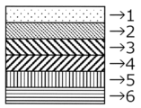
- FIG. 1 is a schematic cross-sectional view showing an example of the structure of a photoelectric conversion element used in the present invention.
- the imaging photoelectric conversion element of the present invention has at least one organic layer between two electrodes and is a photoelectric conversion element that converts light into electrical energy.
- the organic layer contains a material for an imaging photoelectric conversion element made of a compound represented by the above general formula (1). More specifically, in an imaging photoelectric conversion element having a photoelectric conversion layer and an electron blocking layer between two electrodes, at least one of the photoelectric conversion layer and the electron blocking layer contains a material for a photoelectric conversion element made of the above general formula (1).
- the material for an imaging photoelectric conversion element made of a compound represented by general formula (1) will be simply referred to as a material for a photoelectric conversion element. It may also be referred to as the material of the present invention or the compound represented by general formula (1).
- ring B is fused with an adjacent ring at any position to form a 6-membered ring represented by formula (1B).
- Ring C is fused with an adjacent ring at any position to form a 5-membered ring represented by formula (1C).
- X is represented by any of N-Ar 5 , O, S, and C-Ar 6 Ar 7 , but is preferably represented by N-Ar 5 , O, or S, more preferably represented by N-Ar 5 or S, and even more preferably represented by N-Ar 5.
- a, b, and c represent the number of substitutions, and a and b each independently represent an integer of 0 to 4, and c represents an integer of 0 to 2, but it is preferable that each is 0.
- At least one of Ar 1 to Ar 5 contains one or more structures represented by the above general formula (2) and one or more structures represented by the above general formula (3), and among these, it is preferable that Ar 1 contains at least one each of the structures represented by the general formula (2) and the general formula (3).
- Ar 1 to Ar 7 do not contain a nitrogen-containing six-membered ring structure, and it is more preferable that they do not contain a nitrogen-containing six-membered ring structure, and quinoline, isoquinoline, quinazoline, quinoxaline, benzimidazole, aza-triphenylene, phenanthroline, aza-pyrene, aza-anthracene, aza-fluorene, aza-dibenzofuran, aza-dibenzothiophene, aza-dibenzoselenophene, or aza-carbazole.
- Y is independently represented by any one of N-Ar 10 , O, S, C-Ar 11 Ar 12 , preferably N-Ar 10 , O or S, more preferably N-Ar 10 .
- Z is independently represented by any one of O, S, and C-Ar 15 Ar 16 , and is preferably any one of O and S.
- d to g represent the number of substitutions, each independently representing an integer of 0 to 4, preferably 0 to 2, and more preferably 0 to 1.
- Ar 1 to Ar 7 each independently represent deuterium, a halogen, an alkyl group having 1 to 20 carbon atoms, a substituted or unsubstituted aromatic amino group having 12 to 36 carbon atoms, a substituted or unsubstituted aromatic hydrocarbon group having 6 to 18 carbon atoms, a substituted or unsubstituted aromatic heterocyclic group having 3 to 18 carbon atoms, or a substituted or unsubstituted linked aromatic group formed by linking 2 to 10 of these aromatic groups; a substituted or unsubstituted aromatic hydrocarbon group having 6 to 18 carbon atoms or a substituted or unsubstituted aromatic heterocyclic group having 3 to 18 carbon atoms is preferred, a substituted or unsubstituted aromatic hydrocarbon group having 6 to 13 carbon atoms or a substituted or unsubstituted aromatic heterocyclic group having 3 to 17 carbon atoms is more preferred, and a substituted or unsubstituted aromatic hydrocarbon group having 6 to 13 carbon
- Ar 1 to Ar 7 represent a linking aromatic group
- the number of links is preferably 2 to 6, and more preferably 2 to 4.
- Ar 8 to Ar 16 each independently represent deuterium, halogen, an alkyl group having 1 to 20 carbon atoms, a substituted or unsubstituted aromatic amino group having 12 to 36 carbon atoms, a substituted or unsubstituted aromatic hydrocarbon group having 6 to 18 carbon atoms, a substituted or unsubstituted aromatic heterocyclic group having 3 to 18 carbon atoms, or a substituted or unsubstituted linked aromatic group formed by linking 2 to 4 of these aromatic groups, but are preferably substituted or unsubstituted aromatic hydrocarbon groups having 6 to 18 carbon atoms or substituted or unsubstituted aromatic heterocyclic groups having 3 to 18 carbon atoms, more preferably substituted or unsubstituted aromatic hydrocarbon groups having 6 to 13 carbon atoms or substituted or unsubstituted aromatic heterocyclic groups having 3 to 17 carbon
- Ar 8 to Ar 16 represent a linked aromatic group
- the number of links is preferably 2 to 3.
- Ar 1 to Ar 7 are the above aromatic heterocyclic groups and the above linking aromatic groups containing aromatic heterocyclic groups, it is preferable that they do not contain a nitrogen-containing six-membered ring structure, and quinoline, isoquinoline, quinazoline, quinoxaline, benzimidazole, aza-triphenylene, phenanthroline, aza-pyrene, aza-anthracene, aza-fluorene, aza-dibenzofuran, aza-dibenzothiophene, aza-dibenzoselenophene, or aza-carbazole.
- nitrogen-containing six-membered ring examples include pyridine, pyrimidine, pyrazine, pyridazine, triazine, and tetrazine.
- Ar 1 to Ar 7 do not contain a nitrogen-containing six-membered ring structure or the above structure such as quinoline
- Ar 8 to Ar 16 also do not contain a nitrogen-containing six-membered ring structure or the above structure such as quinoline.
- Ar 1 to Ar 16 are groups having a hydrogen atom, the hydrogen atom may be substituted with deuterium or a halogen.
- Ar 1 contains at least one each of the structure represented by the general formula (2) and the structure represented by the general formula (3), it is preferably represented by any one of the following formulas (4) to (7), more preferably represented by any one of the formulas (4), (5), or (7), and further preferably represented by any one of the formulas (4) or (7).
- L 1 and L 2 each independently represent a direct bond, a substituted or unsubstituted aromatic hydrocarbon group having 6 to 18 carbon atoms, or a substituted or unsubstituted linked aromatic group formed by linking 2 to 6 of these aromatic groups, preferably a direct bond or a substituted or unsubstituted aromatic hydrocarbon group having 6 to 18 carbon atoms, and more preferably a direct bond or a substituted or unsubstituted aromatic hydrocarbon group having 6 to 12 carbon atoms.
- L 1 and L 2 are unsubstituted aromatic hydrocarbon groups having 6 to 18 carbon atoms are the same as specific examples when Ar 1 to Ar 16 are unsubstituted aromatic hydrocarbon groups having 6 to 18 carbon atoms, except that they are groups obtained by removing two hydrogen atoms from known aromatic hydrocarbons.
- the form of the general formula (1) is represented by any one of the following formulas (8) to (13), and is preferably represented by formulas (8), (9), (10), or (12), and more preferably represented by formulas (8), (9), or (12).
- Ar 1 to Ar 16 are halogen include a fluoro group, a chloro group, a bromo group, and an iodo group, with a fluoro group being preferred.
- Ar 1 to Ar 16 are alkyl groups having 1 to 20 carbon atoms, they may be any of linear, branched, and cyclic alkyl groups, and are preferably linear, branched, or cyclic alkyl groups having 1 to 10 carbon atoms.
- linear saturated hydrocarbon groups such as methyl, ethyl, n-propyl, n-butyl, n-pentyl, n-hexyl, n-octyl, n-dodecyl, n-tetradecyl, and n-octadecyl groups
- branched saturated hydrocarbon groups such as isopropyl, isobutyl, neopentyl, 2-ethylhexyl, and 2-hexyloctyl groups
- saturated alicyclic hydrocarbon groups such as cyclopentyl, cyclohexyl, cyclooctyl, and 4-butylcyclohexyl groups.
- aryl group of the unsubstituted aromatic amino group of Ar 1 to Ar 16 include groups in which one hydrogen atom has been removed from phenyl, biphenyl, terphenyl, quaterphenyl, naphthyl, phenanthrenyl, anthracenyl, triphenylenyl, pyrenyl, fluorenyl, spirobifluorenyl, etc., and preferred are phenyl, biphenyl, terphenyl , naphthyl, phenanthrenyl, fluorenyl, and triphenylenyl.
- heteroaryl groups in which 16 is an unsubstituted aromatic amino group include pyrrole, pyrrolopyrrole, indole, pyrroloindole, benzoindole, naphthopyrrole, isoindole, pyrroloisoindole, benzisoindole, naphthoisopyrrole, carbazole, benzocarbazole, indoloindole, carbazolocarbazole, benzofurocarbazole, benzothienocarbazole, carboline, thiophene, benzothiophene, naphthothiophene, dibenzothiophene, benzothienonaphthalene, benzothienobenzothiophene, and benzothienodiben.
- Examples of such groups include groups in which one hydrogen atom has been removed from zothiophene, dinaphthothiophene, dinaphthothienothiophene, naphthobenzothiophene, furan, benzofuran, naphthofuran, dibenzofuran, benzofuronaphthalene, benzofurobenzofuran, benzofurodibenzofuran, dinaphthofuranofuran, naphthobenzofuran, pyridine, pyrimidine, triazine, quinoline, isoquinoline, quinazoline, quinoxaline, and the like, and preferably dibenzofuran, dibenzothiophene, carbazole, benzofurocarbazole, or benzothienocarbazole.
- aromatic hydrocarbon examples include groups in which one hydrogen has been removed from known aromatic hydrocarbons.
- aromatic hydrocarbon examples include monocyclic aromatic hydrocarbons such as benzene, bicyclic aromatic hydrocarbons such as naphthalene, tricyclic aromatic hydrocarbons such as indacene, biphenylene, phenalene, anthracene, phenanthrene, and fluorene, and tetracyclic aromatic hydrocarbons such as fluoranthene, acephenanthrylene, aceanthrylene, triphenylene, pyrene, chrysene, tetraphene, tetracene, and pleiadene. Benzene, naphthalene, anthracene, triphenylene, and pyrene are preferred.
- Ar 1 to Ar 16 are aromatic heterocyclic groups having 3 to 18 carbon atoms, specific examples thereof include groups in which one hydrogen has been removed from an aromatic heterocyclic group.
- the aromatic heterocyclic group include nitrogen-containing aromatic compounds having a pyrrole ring such as pyrrole, pyrrolopyrrole, indole, pyrroloindole, benzoindole, naphthopyrrole, isoindole, pyrroloisoindole, benzoisoindole, naphthoisopyrrole, carbazole, benzocarbazole, indoloindole, carbazolocarbazole, indolocarbazole, and carboline; thiophene, benzothiophene, naphthothiophene, dibenzothiophene, benzothienonaphthalene, benzothienobenzothiophene, and benzothienodibenzothiophene.
- aromatic ring examples include sulfur-containing aromatic compounds having a thiophene ring such as phene, dinaphthothiophene, dinaphthothienothiophene, naphthobenzothiophene, and benzothienocarbazole, oxygen-containing aromatic compounds having a furan ring such as furan, benzofuran, naphthofuran, dibenzofuran, benzofuronaphthalene, benzofurobenzofuran, benzofurodibenzofuran, dinaphthofuran, dinaphthofuranofuran, naphthobenzofuran, and benzofurocarbazole, pyridine, pyrimidine, triazine, quinoline, isoquinoline, quinazoline, and quinoxaline.
- sulfur-containing aromatic compounds having a thiophene ring such as phene, dinaphthothiophene, dinaphthothienothi
- dibenzofuran, dibenzothiophene, carbazole benzothienodibenzothiophene, benzofurodibenzofuran, indolocarbazole, benzofurocarbazole, or benzothienocarbazole, and more preferably dibenzofuran, dibenzothiophene, and carbazole.
- a linking aromatic group refers to an aromatic group in which the aromatic rings of two or more aromatic groups are linked by single bonds. These linking aromatic groups may be linear or branched. The linking position when the benzene rings are linked together may be ortho, meta, or para, but is preferably a para or meta linking.
- the aromatic group may be an aromatic hydrocarbon group or an aromatic heterocyclic group, and the multiple aromatic groups may be the same or different. The aromatic groups that constitute the linking aromatic group do not include aromatic amino groups.
- Ar 1 to Ar 16 and L 1 to L 2 are aromatic hydrocarbon groups, aromatic heterocyclic groups, or linking aromatic groups, they may have a substituent, and examples of the substituent include deuterium, halogen, an alkyl group having 1 to 20 carbon atoms, an aralkyl group having 7 to 38 carbon atoms, an alkenyl group having 2 to 20 carbon atoms, an alkynyl group having 2 to 20 carbon atoms, an acyl group having 2 to 20 carbon atoms, an acyloxy group having 2 to 20 carbon atoms, an alkoxy group having 1 to 20 carbon atoms, an alkoxycarbonyl group having 2 to 20 carbon atoms, an alkoxycarbonyloxy group having 2 to 20 carbon atoms, an alkylsulfonyl group having 1 to 20 carbon atoms, and an alkylsilyl group having 3 to 12 carbon atoms.
- Ar 1 to Ar 16 are aromatic amino groups
- the aromatic group may have a substituent, and examples of
- the alkyl group having 1 to 20 carbon atoms as the substituent may be any of linear, branched, and cyclic alkyl groups, and is preferably a linear, branched, or cyclic alkyl group having 1 to 10 carbon atoms.
- linear saturated hydrocarbon groups such as methyl, ethyl, n-propyl, n-butyl, n-pentyl, n-hexyl, n-octyl, n-dodecyl, n-tetradecyl, and n-octadecyl groups; branched saturated hydrocarbon groups such as isopropyl, isobutyl, neopentyl, 2-ethylhexyl, and 2-hexyloctyl groups; and saturated alicyclic hydrocarbon groups such as cyclopentyl, cyclohexyl, cyclooctyl, 4-butylcyclohexyl, and 4-dodecylcyclohexyl groups.
- halogen as the substituent include a fluoro group, a chloro group, a bromo group, and an iodo group.
- aralkyl group having 7 to 38 carbon atoms as the substituent include a benzyl group, a phenethyl group, a phenylpropyl group, a phenylbutyl group, a naphthylmethyl group, and a triphenylenylmethyl group.
- alkenyl group having 2 to 20 carbon atoms as the substituent include an ethylene group, a propylene group, a butylene group, a pentene group, a cyclopentene group, a hexene group, a cyclohexene group, and an octene group.
- alkynyl group having 2 to 20 carbon atoms as the substituent include an acetylene group, a propyne group,
- alkoxycarbonyl group having 2 to 20 carbon atoms as the substituent include a methoxycarbonyl group and an ethoxycarbonyl group.
- alkylsilyl group having 3 to 12 carbon atoms as the substituent include a trimethylsilyl group, a triethylsilyl group, and a tripropylsilyl group.
- Specific examples of the alkoxycarbonyloxy group include a methoxycarbonyloxy group, an ethoxycarbonyloxy group, and a butoxycarbonyloxy group.
- Specific examples of the alkylsulfonyl group include a methylsulfonyl group, an ethylsulfonyl group, and a propylsulfonyl group.
- the compound represented by the general formula (1) of the present invention can be obtained by synthesizing it using various organic synthesis reactions established in the field of organic synthetic chemistry, including coupling reactions such as Suzuki coupling, Stille coupling, Grignard coupling, Ullmann coupling, Buchwald-Hartwig reaction, and Heck reaction, using commercially available reagents as raw materials, and then purifying it using known methods such as recrystallization, column chromatography, and sublimation purification, but is not limited to this method.
- the photoelectric conversion element material of the present invention preferably has an energy level of the highest occupied molecular orbital (HOMO) obtained by structural optimization calculation using density functional calculation B3LYP/6-31G(d) of -4.3 eV or less, more preferably in the range of -5.5 eV to -4.5 eV, and even more preferably in the range of -5.2 eV to -4.8 eV.
- HOMO highest occupied molecular orbital
- the photoelectric conversion element material of the present invention preferably has an energy level of the lowest unoccupied molecular orbital (LUMO) obtained by structural optimization calculation using density functional calculation B3LYP/6-31G(d) of -2.5 eV or higher, more preferably in the range of -2.0 eV to -0.5 eV, and even more preferably in the range of -1.5 eV to -0.5 eV.
- LUMO lowest unoccupied molecular orbital
- the material for photoelectric conversion elements of the present invention preferably has a difference (absolute value) between the HOMO energy level and the LUMO energy level in the range of 2.0 eV to 5.0 eV, more preferably in the range of 2.5 eV to 4.7 eV, and even more preferably in the range of 3.5 eV to 4.5 eV.
- the material for photoelectric conversion devices of the present invention preferably has a hole mobility of 1 ⁇ 10 ⁇ 6 cm 2 /Vs or more, more preferably 1 ⁇ 10 ⁇ 5 cm 2 /Vs to 1 ⁇ 10 ⁇ 1 cm 2 /Vs, and even more preferably 8 ⁇ 10 ⁇ 5 cm 2 /Vs to 1 ⁇ 10 ⁇ 2 cm 2 /Vs.
- the hole mobility can be evaluated by known methods such as a method using a FET transistor element, a method using a time-of-flight method, or an SCLC method.
- the photoelectric conversion element material of the present invention is preferably amorphous.
- the fact that it is amorphous can be confirmed by various methods, for example, by the absence of detection of a peak by the XRD method or the absence of detection of an endothermic peak by the DSC method.
- FIG. 1 is a cross-sectional view showing a schematic example of the structure of an imaging photoelectric conversion element of the present invention, in which 1 represents an electrode, 2 represents a hole blocking layer, 3 represents a photoelectric conversion layer, 4 represents an electron blocking layer, 5 represents an electrode, and 6 represents a substrate. Note that the configuration excluding the substrate may be reversed from that shown in Fig. 1, i.e., 1 represents a substrate, 2 represents an electrode, 3 represents an electron blocking layer, 4 represents a photoelectric conversion layer, 5 represents a hole blocking layer, and 6 represents an electrode.
- the structure is not limited to that shown in Fig. 1, and layers can be added or omitted as necessary.
- the electrode used in the imaging photoelectric conversion element using the imaging photoelectric conversion element material of the present invention has a function of collecting holes and electrons generated in the photoelectric conversion layer. In addition, a function of allowing light to enter the photoelectric conversion layer is also required. Therefore, it is desirable that at least one of the two electrodes is transparent or semi-transparent.
- the material used as the electrode is not particularly limited as long as it has conductivity, and examples thereof include conductive transparent materials such as ITO, IZO, SnO 2 , ATO (antimony-doped tin oxide), ZnO, AZO (Al-doped zinc oxide), GZO (gallium-doped zinc oxide), TiO 2 and FTO, metals such as gold, silver, platinum, chromium, aluminum, iron, cobalt, nickel and tungsten, inorganic conductive materials such as copper iodide and copper sulfide, conductive polymers such as polythiophene, polypyrrole and polyaniline, etc. These materials may be mixed and used as necessary. In addition, two or more layers may be laminated.
- conductive transparent materials such as ITO, IZO, SnO 2 , ATO (antimony-doped tin oxide), ZnO, AZO (Al-doped zinc oxide), GZO (gallium-doped zinc oxide
- the photoelectric conversion layer is a layer in which holes and electrons are generated by charge separation of excitons generated by incident light.
- the photoelectric conversion layer may be formed of a single photoelectric conversion material, but may also be formed in combination with a P-type organic semiconductor material that is a hole transport material or an N-type organic semiconductor material that is an electron transport material. Two or more types of P-type organic semiconductors may be used, or two or more types of N-type organic semiconductors may be used. It is desirable to use a dye material having a function of absorbing light of a desired wavelength in the visible region as one or more of these P-type organic semiconductors and/or N-type semiconductors.
- the P-type organic semiconductor material that is a hole transport material the compound represented by the general formula (1) of the present invention can be used.
- the P-type organic semiconductor material may be any material having hole transport properties. It is preferable to use a material represented by general formula (1), but other P-type organic semiconductor materials may also be used. Two or more materials represented by general formula (1) may be mixed and used. Furthermore, a compound represented by general formula (1) may be mixed with other P-type organic semiconductor materials.
- the other P-type organic semiconductor material may be any material having hole transport properties, and examples of such materials that can be used include compounds having a condensed polycyclic aromatic group such as naphthalene, anthracene, phenanthrene, pyrene, chrysene, naphthacene, triphenylene, perylene, fluoranthene, fluorene, and indene, compounds having a ⁇ -excess aromatic group such as cyclopentadiene derivatives, furan derivatives, thiophene derivatives, pyrrole derivatives, benzofuran derivatives, benzothiophene derivatives, dinaphthothienothiophene derivatives, indole derivatives, pyrazoline derivatives, dibenzofuran derivatives, dibenzothiophene derivatives, carbazole derivatives, and indolocarbazole derivatives, aromatic amine derivatives, styrylamine derivatives, benzidine derivatives, porphyrin
- a polymer-type P-type organic semiconductor material may be used as the other P-type organic semiconductor material.
- Specific examples include polyphenylenevinylene derivatives, polyparaphenylene derivatives, polyfluorene derivatives, polyvinylcarbazole derivatives, and polythiophene derivatives.
- a compound represented by general formula (1) may be used in combination with two or more compounds selected from the P-type organic semiconductor materials and the polymer-type P-type organic semiconductor materials.
- the N-type organic semiconductor material may be any material that has electron transport properties, and examples of such materials include naphthalenetetracarboxylic acid diimide, perylenetetracarboxylic acid diimide, fullerenes, and azole derivatives such as imidazole, thiazole, thiadiazole, oxazole, oxadiazole, and triazole. Two or more compounds selected from these N-type organic semiconductor materials may be mixed and used.
- the electron blocking layer is provided to suppress dark current caused by injection of electrons from one electrode into the photoelectric conversion layer when a bias voltage is applied between the two electrodes. It also has a function as a hole transporter that transports holes generated by charge separation in the photoelectric conversion layer to the electrode, and a single layer or multiple layers can be arranged as necessary.
- the electron blocking layer can be made of a P-type organic semiconductor material that is a hole transport material.
- the P-type organic semiconductor material any material having hole transport properties is sufficient, and it is preferable to use a compound represented by general formula (1), but other P-type organic semiconductor materials may also be used.
- the compound represented by general formula (1) may be mixed with other P-type organic semiconductor materials.
- the other P-type organic semiconductor material any material having hole transport properties is sufficient, and specifically, the compounds exemplified as other P-type organic semiconductor materials at the photoelectric conversion layer are exemplified.
- a polymeric P-type organic semiconductor material may be used as the other P-type organic semiconductor material.
- Specific examples thereof include the compounds exemplified as the polymeric P-type organic semiconductor material in the photoelectric conversion layer.
- a mixture of two or more compounds selected from the compound represented by general formula (1) of the present invention, the P-type organic semiconductor material, or the polymeric P-type organic semiconductor material may be used.
- the hole blocking layer is provided to suppress dark current caused by holes being injected from one electrode into the photoelectric conversion layer when a bias voltage is applied between the two electrodes. It also has a function of transporting electrons generated by charge separation in the photoelectric conversion layer to the electrode, and a single layer or multiple layers can be arranged as necessary.
- the hole blocking layer can be made of an N-type organic semiconductor having electron transport properties.
- the N-type organic semiconductor material may be any material having electron transport properties, and examples thereof include polycyclic aromatic polycarboxylic anhydrides and imidized products thereof, such as naphthalene tetracarboxylic diimide and perylene tetracarboxylic diimide, fullerenes such as C60 and C70, azole derivatives such as imidazole, thiazole, thiadiazole, oxazole, oxadiazole, and triazole, tris(8-quinolinolato)aluminum(III) derivatives, phosphine oxide derivatives, nitro-substituted fluorene derivatives, diphenylquinone derivatives, thiopyran dioxide derivatives, carbodiimide derivatives, fluorenylidene methane derivatives, anthraquinodimethane derivatives and anthrone derivatives, bipyridine derivatives, quinoline derivatives, and indolocarbazole derivative
- the hydrogen in the photoelectric conversion element material of the present invention may be deuterium. That is, in addition to the hydrogen on the aromatic ring in general formula (1), some or all of the hydrogen in the substituent may be deuterium. Furthermore, some or all of the hydrogen in the compound used as the N-type organic semiconductor material and the P-type organic semiconductor material may be deuterium.
- each layer is not particularly limited, and they may be produced by either a dry process or a wet process.
- the organic layer containing the material for the photoelectric conversion element of the present invention may be a multi-layer structure, if necessary.
- the imaging photoelectric conversion element of the present application preferably has a current value in a dark place of 5.3 ⁇ 10 ⁇ 10 A/cm 2 or less, more preferably 1.0 ⁇ 10 ⁇ 12 A/cm 2 to 5.3 ⁇ 10 ⁇ 10 A/cm 2, and even more preferably 1.0 ⁇ 10 ⁇ 12 A/cm 2 to 4.5 ⁇ 10 ⁇ 10 A/cm 2 , under the measurement conditions described in Example 1 of the present application.
- the imaging photoelectric conversion element of the present application preferably has a light/dark ratio of 6.0 ⁇ 10 2 or more, more preferably 7.0 ⁇ 10 2 or more, and even more preferably 7.5 ⁇ 10 2 or more , under the measurement conditions described in Example 1 of the present application.
- Synthesis Example 2 (Synthesis of Intermediate R5)
- R4 (19.5 mmol) R3 (21.5 mmol) synthesized in Synthesis Example 1, and tripotassium phosphate (39.0 mmol) were charged into a 500 ml three-neck flask that had been degassed and replaced with nitrogen, and 50 ml of dimethylimidazolidinone was added to the mixture, followed by stirring at 180°C for 8 hours. After cooling to room temperature, inorganic matter was removed by filtration, and 200 ml of water and 200 ml of dichloromethane were added to the filtrate, which was then transferred to a separatory funnel and fractionated into an organic layer and an aqueous layer.
- Synthesis Example 3 (Synthesis of A05) R5 (8.5 mmol), R6 (127.6 mmol), copper powder (25.5 mmol), and potassium carbonate (42.5 mmol) synthesized in Synthesis Example 2 were added to a 500 ml three-neck flask that had been degassed and replaced with nitrogen, and the mixture was stirred at 180°C for 8 hours. After cooling to room temperature, inorganic substances were removed by filtration, and 200 ml of water and 200 ml of dichloromethane were added to the filtrate, which was then transferred to a separatory funnel and fractionated into an organic layer and an aqueous layer.
- Example 1 On an electrode made of ITO with a film thickness of 70 nm formed on a glass substrate, a film of compound A05 was formed to a thickness of 10 nm as an electron blocking layer at a vacuum degree of 4.0 ⁇ 10 ⁇ 5 Pa. Next, as a photoelectric conversion layer, 2Ph-BTBT, F6-SubPc-OC6F5, and fullerene (C60) were co-evaporated to a thickness of 200 nm at an evaporation rate ratio of 4:4:2 to form a film. Subsequently, dpy-NDI was evaporated to a thickness of 10 nm to form a hole blocking layer.
- Examples 2 to 9 A photoelectric conversion element was prepared in the same manner as in Example 1, except that the compound shown in Table 3 was used for the electron blocking layer.
- Comparative Examples 1 to 4 Photoelectric conversion elements were prepared in the same manner as in Example 1, except that the compounds shown in Table 3 were used for the electron blocking layer. The results of Examples 1 to 9 and Comparative Examples 1 to 4 are shown in Table 3.
- the material for photoelectric conversion elements for imaging of the present invention By using the material for photoelectric conversion elements for imaging of the present invention, appropriate movement of holes and electrons can be achieved within the photoelectric conversion element for imaging, which makes it possible to reduce the leakage current caused by application of a bias voltage when converting light into electrical energy. As a result, it is believed that a photoelectric conversion element that achieves a low dark current value and a high light-dark ratio can be obtained. Therefore, the material of the present invention is useful as a material for photoelectric conversion elements in photoelectric conversion film stacked imaging devices.
- Electrode 2 Hole blocking layer 3 Photoelectric conversion layer 4 Electron blocking layer 5 Electrode 6 Substrate
Landscapes
- Chemical & Material Sciences (AREA)
- Organic Chemistry (AREA)
- Physics & Mathematics (AREA)
- Electromagnetism (AREA)
- Spectroscopy & Molecular Physics (AREA)
- Engineering & Computer Science (AREA)
- Materials Engineering (AREA)
- Light Receiving Elements (AREA)
- Heterocyclic Carbon Compounds Containing A Hetero Ring Having Oxygen Or Sulfur (AREA)
Priority Applications (3)
| Application Number | Priority Date | Filing Date | Title |
|---|---|---|---|
| CN202480033279.5A CN121220211A (zh) | 2023-07-14 | 2024-07-09 | 光电转换元件用材料及使用其的光电转换元件 |
| JP2025533999A JPWO2025018226A1 (cg-RX-API-DMAC7.html) | 2023-07-14 | 2024-07-09 | |
| KR1020267003811A KR20260041819A (ko) | 2023-07-14 | 2024-07-09 | 광전 변환 소자용 재료 및 이것을 사용한 광전 변환 소자 |
Applications Claiming Priority (2)
| Application Number | Priority Date | Filing Date | Title |
|---|---|---|---|
| JP2023116154 | 2023-07-14 | ||
| JP2023-116154 | 2023-07-14 |
Publications (1)
| Publication Number | Publication Date |
|---|---|
| WO2025018226A1 true WO2025018226A1 (ja) | 2025-01-23 |
Family
ID=94281894
Family Applications (1)
| Application Number | Title | Priority Date | Filing Date |
|---|---|---|---|
| PCT/JP2024/024781 Ceased WO2025018226A1 (ja) | 2023-07-14 | 2024-07-09 | 光電変換素子用材料及びこれを用いた光電変換素子 |
Country Status (5)
| Country | Link |
|---|---|
| JP (1) | JPWO2025018226A1 (cg-RX-API-DMAC7.html) |
| KR (1) | KR20260041819A (cg-RX-API-DMAC7.html) |
| CN (1) | CN121220211A (cg-RX-API-DMAC7.html) |
| TW (1) | TW202502772A (cg-RX-API-DMAC7.html) |
| WO (1) | WO2025018226A1 (cg-RX-API-DMAC7.html) |
Citations (4)
| Publication number | Priority date | Publication date | Assignee | Title |
|---|---|---|---|---|
| JP2011213724A (ja) * | 2010-04-01 | 2011-10-27 | Samsung Mobile Display Co Ltd | 縮合環化合物及びそれを含む有機発光素子 |
| WO2013088973A1 (ja) * | 2011-12-15 | 2013-06-20 | 新日鉄住金化学株式会社 | 有機電界発光素子 |
| JP2018085427A (ja) * | 2016-11-22 | 2018-05-31 | ソニー株式会社 | 撮像素子、積層型撮像素子、撮像装置及び電子装置 |
| CN113980026A (zh) * | 2021-11-25 | 2022-01-28 | 上海钥熠电子科技有限公司 | 咔唑衍生物类胺化合物和包含其的有机电致发光器件 |
Family Cites Families (4)
| Publication number | Priority date | Publication date | Assignee | Title |
|---|---|---|---|---|
| TWI491584B (zh) | 2009-09-11 | 2015-07-11 | 富士軟片股份有限公司 | 光電轉換元件及其製造方法、光感測器、影像元件及它們的驅動方法 |
| KR20170140989A (ko) | 2016-06-14 | 2017-12-22 | 삼성전자주식회사 | 축합환 화합물 및 이를 포함한 유기 발광 소자 |
| TWI915452B (zh) | 2020-11-27 | 2026-02-21 | 日商日鐵化學材料股份有限公司 | 攝像用的光電轉換元件材料及光電轉換元件 |
| TWI899379B (zh) | 2020-11-27 | 2025-10-01 | 日商日鐵化學材料股份有限公司 | 攝像用光電轉換元件 |
-
2024
- 2024-07-09 JP JP2025533999A patent/JPWO2025018226A1/ja active Pending
- 2024-07-09 KR KR1020267003811A patent/KR20260041819A/ko active Pending
- 2024-07-09 CN CN202480033279.5A patent/CN121220211A/zh active Pending
- 2024-07-09 WO PCT/JP2024/024781 patent/WO2025018226A1/ja not_active Ceased
- 2024-07-10 TW TW113125889A patent/TW202502772A/zh unknown
Patent Citations (4)
| Publication number | Priority date | Publication date | Assignee | Title |
|---|---|---|---|---|
| JP2011213724A (ja) * | 2010-04-01 | 2011-10-27 | Samsung Mobile Display Co Ltd | 縮合環化合物及びそれを含む有機発光素子 |
| WO2013088973A1 (ja) * | 2011-12-15 | 2013-06-20 | 新日鉄住金化学株式会社 | 有機電界発光素子 |
| JP2018085427A (ja) * | 2016-11-22 | 2018-05-31 | ソニー株式会社 | 撮像素子、積層型撮像素子、撮像装置及び電子装置 |
| CN113980026A (zh) * | 2021-11-25 | 2022-01-28 | 上海钥熠电子科技有限公司 | 咔唑衍生物类胺化合物和包含其的有机电致发光器件 |
Also Published As
| Publication number | Publication date |
|---|---|
| JPWO2025018226A1 (cg-RX-API-DMAC7.html) | 2025-01-23 |
| TW202502772A (zh) | 2025-01-16 |
| CN121220211A (zh) | 2025-12-26 |
| KR20260041819A (ko) | 2026-03-27 |
Similar Documents
| Publication | Publication Date | Title |
|---|---|---|
| JP7811552B2 (ja) | 撮像用の光電変換素子材料及び光電変換素子 | |
| KR102709386B1 (ko) | 아릴아민 화합물 및 이를 포함하는 유기 전계 발광 소자, 전자 장치 | |
| TWI899379B (zh) | 攝像用光電轉換元件 | |
| WO2024135588A1 (ja) | 光電変換素子用材料を含む光電変換素子 | |
| KR20240035755A (ko) | 촬상용의 광전 변환 소자용 재료 및 촬상용 광전 변환 소자 | |
| WO2024195391A1 (ja) | 光電変換素子 | |
| WO2025018227A1 (ja) | 光電変換素子用材料及びこれを用いた光電変換素子 | |
| WO2023228974A1 (ja) | 撮像用の光電変換素子用材料及びこれを用いた撮像用光電変換素子 | |
| WO2024057957A1 (ja) | 光電変換素子用材料及びこれを用いた光電変換素子 | |
| TW202502772A (zh) | 包含光電轉換元件用材料的光電轉換元件及攝像用的光電轉換元件 | |
| WO2024057958A1 (ja) | 光電変換素子用材料及び光電変換素子 | |
| WO2024135589A1 (ja) | 光電変換素子用材料を含む光電変換素子 | |
| WO2023228922A1 (ja) | 撮像用の光電変換素子用材料及び光電変換素子 | |
| TW202311238A (zh) | 攝像用的光電轉換元件用材料以及光電轉換元件 | |
| TW202330500A (zh) | 攝像用的光電轉換元件用材料以及光電轉換元件 | |
| WO2023140173A1 (ja) | 撮像用の光電変換素子用材料及び光電変換素子 |
Legal Events
| Date | Code | Title | Description |
|---|---|---|---|
| 121 | Ep: the epo has been informed by wipo that ep was designated in this application |
Ref document number: 24843018 Country of ref document: EP Kind code of ref document: A1 |
|
| ENP | Entry into the national phase |
Ref document number: 2025533999 Country of ref document: JP Kind code of ref document: A |
|
| ENP | Entry into the national phase |
Ref document number: 1020267003811 Country of ref document: KR Free format text: ST27 STATUS EVENT CODE: A-0-1-A10-A15-NAP-PA0105 (AS PROVIDED BY THE NATIONAL OFFICE) |
|
| WWE | Wipo information: entry into national phase |
Ref document number: 1020267003811 Country of ref document: KR |
|
| NENP | Non-entry into the national phase |
Ref country code: DE |
|
| WWP | Wipo information: published in national office |
Ref document number: 1020267003811 Country of ref document: KR |
|
| 122 | Ep: pct application non-entry in european phase |
Ref document number: 24843018 Country of ref document: EP Kind code of ref document: A1 |