WO2025017891A1 - 光ファイバセンシング方法 - Google Patents
光ファイバセンシング方法 Download PDFInfo
- Publication number
- WO2025017891A1 WO2025017891A1 PCT/JP2023/026507 JP2023026507W WO2025017891A1 WO 2025017891 A1 WO2025017891 A1 WO 2025017891A1 JP 2023026507 W JP2023026507 W JP 2023026507W WO 2025017891 A1 WO2025017891 A1 WO 2025017891A1
- Authority
- WO
- WIPO (PCT)
- Prior art keywords
- optical
- communication
- switch
- optical switch
- sensing
- Prior art date
- Legal status (The legal status is an assumption and is not a legal conclusion. Google has not performed a legal analysis and makes no representation as to the accuracy of the status listed.)
- Pending
Links
Images


Classifications
-
- G—PHYSICS
- G01—MEASURING; TESTING
- G01D—MEASURING NOT SPECIALLY ADAPTED FOR A SPECIFIC VARIABLE; ARRANGEMENTS FOR MEASURING TWO OR MORE VARIABLES NOT COVERED IN A SINGLE OTHER SUBCLASS; TARIFF METERING APPARATUS; MEASURING OR TESTING NOT OTHERWISE PROVIDED FOR
- G01D5/00—Mechanical means for transferring the output of a sensing member; Means for converting the output of a sensing member to another variable where the form or nature of the sensing member does not constrain the means for converting; Transducers not specially adapted for a specific variable
- G01D5/26—Mechanical means for transferring the output of a sensing member; Means for converting the output of a sensing member to another variable where the form or nature of the sensing member does not constrain the means for converting; Transducers not specially adapted for a specific variable characterised by optical transfer means, i.e. using infrared, visible, or ultraviolet light
- G01D5/32—Mechanical means for transferring the output of a sensing member; Means for converting the output of a sensing member to another variable where the form or nature of the sensing member does not constrain the means for converting; Transducers not specially adapted for a specific variable characterised by optical transfer means, i.e. using infrared, visible, or ultraviolet light with attenuation or whole or partial obturation of beams of light
- G01D5/34—Mechanical means for transferring the output of a sensing member; Means for converting the output of a sensing member to another variable where the form or nature of the sensing member does not constrain the means for converting; Transducers not specially adapted for a specific variable characterised by optical transfer means, i.e. using infrared, visible, or ultraviolet light with attenuation or whole or partial obturation of beams of light the beams of light being detected by photocells
- G01D5/353—Mechanical means for transferring the output of a sensing member; Means for converting the output of a sensing member to another variable where the form or nature of the sensing member does not constrain the means for converting; Transducers not specially adapted for a specific variable characterised by optical transfer means, i.e. using infrared, visible, or ultraviolet light with attenuation or whole or partial obturation of beams of light the beams of light being detected by photocells influencing the transmission properties of an optical fibre
Definitions
- This disclosure relates to optical fiber sensing technology.
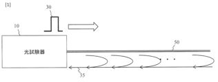
- FIG. 1 is a diagram explaining optical fiber sensing.
- Optical fiber sensing is an optical measurement technology that receives backscattered light 35 generated by test light 30 incident on an optical fiber 50 and measures the distribution of the state of the optical fiber 50.
- Optical fiber sensing has the following characteristics (for example, see Non-Patent Document 1):
- Measurements can be made at only one end of the optical fiber (there is no need to install a device at the other end).
- An optical pulse or CW (continuous wave) test light is input and the backscattered light generated in the optical fiber is observed.
- Backscattered light can be Rayleigh scattering, Brillouin scattering, Raman scattering, etc.
- a disturbance bending, temperature change, strain, vibration, etc.
- its state changes
- the state of the backscattered light also changes along with the state change. Observing the change in state of the backscattered light is equivalent to observing the change in state of the optical fiber, and it is possible to observe the state of the disturbance applied.
- the optical fiber is regarded as a sensor and the backscattered light is observed, it is possible to measure or estimate the disturbance applied to the optical fiber (bending, temperature change, strain change, vibration, etc.).
- the disturbances that can be measured depend on the measurement method and the type of scattered light being observed.
- FIG. 2 is a diagram explaining a DAS system.
- the DAS system includes a light source 11, an optical coupler 12, a modulator 13, an optical amplifier 14, an optical circulator 15, an optical fiber 50 to be measured, a control unit 17, a coupler + balanced PD 18, a digitization means 19, and a calculator 20.
- the DAS system in Figure 2 can obtain backscattered light waveforms 41 as shown in Figure 3 by coherently detecting the backscattered light.
- the interval between light pulses incident on the optical fiber is equal to or greater than the time it takes for light to travel back and forth through the optical fiber 50.
- Adding and averaging these multiple waveforms 41 results in a waveform that can be obtained with a so-called coherent OTDR, making it possible to measure a high S/N ratio.
- arranging these waveforms 41 in pulse order makes it possible to measure the time change in scattered light at each scattering position, in other words, vibration measurement.
- optical pulses with different optical frequencies may be input to the optical fiber 50 (FDM DAS).
- FDM DAS optical frequency multiplexing
- an interval D is required as shown in Fig. 3.
- optical pulses with different optical frequencies can be input to the optical fiber 50 without waiting for the time it takes for light to travel back and forth through the optical fiber 50 as shown in Fig. 4, so that a larger number of waveforms 42 1 to 42 5 can be obtained within the same time period than in the case of one optical frequency.
- ROADM optical fibers by wavelength
- Open ROADM an organization called Open ROADM has defined the functions of ROADM (see, for example, non-patent document 3).
- FIG. 5 is a diagram explaining the structure of ROADM 26.
- optical switches such as ROADM 26 in a WDM transmission system use a wavelength switch 26a on the core network side to select the transmission/reception direction for optical fiber 52 on the core network side by wavelength.
- the optical switch On the user side, the optical switch has, for example, an optical branching unit 26b, and transmits an optical signal from wavelength switch 26a to any user device via optical branching unit 26b.
- the optical switch also receives an optical signal from a user device and transmits it to optical fiber 52 in a direction according to the wavelength.
- APN all optical network
- optical fiber sensing technology In the optical fiber sensing technology described above, test light is input into one optical fiber, and backscattered light that propagates in the reverse direction through the same optical fiber from various points in the optical fiber and returns to the optical fiber sensing device is measured. Therefore, when trying to measure many optical fibers that are laid out as communication fibers using one optical fiber sensing device as in Non-Patent Document 2, optical fiber selection using an optical switch is required, but the following problems arise. (1) Because an optical fiber network contains many optical fibers and optical switches, in order to perform simultaneous, planar measurements of an entire area using an optical fiber network with a single optical fiber sensing device, it is necessary to take into account the equipment configuration, such as the function, configuration, and wiring of the optical switches. (2) The equipment configuration must not affect the communication functions or performance of the optical fiber network. In other words, there has been a problem in that it is difficult to perform optical fiber sensing for an optical fiber network including a plurality of optical fibers and a plurality of optical switches using a single optical fiber sensing device.
- the present invention aims to solve the above problems by providing an optical fiber sensing device and method that enables simultaneous surface measurement of an entire area using an optical fiber network that includes multiple optical fibers and multiple optical switches.
- the optical fiber sensing device of the present invention uses a sensing optical switch to select a communication optical switch included in the optical fiber network, and also controls the communication optical switch so that an optical pulse propagates to the desired optical fiber included in the optical fiber network.
- the optical fiber sensing device comprises: an optical pulse tester that outputs optical pulses at intervals T; a sensing optical switch that connects a plurality of communication optical switches to which a plurality of optical fibers are connected in an existing optical fiber network and the communication optical switches of the existing optical fiber network and the optical pulse tester; a controller that instructs switching of paths of the communication optical switch and the sensing optical switch; Equipped with The controller:
- the optical pulse tester controls the distribution of optical pulses instructing switching of the paths so that the optical pulses from the optical pulse tester are sequentially input to all paths to be sensed among the paths formed by the optical fibers.
- the optical fiber sensing method includes: an optical fiber network including a plurality of communication optical switches to which a plurality of optical fibers are connected, and connecting the communication optical switches and one optical pulse tester through one sensing optical switch; outputting optical pulses at intervals T from the optical pulse tester; and performing distribution control to instruct switching of the communication optical switch and the sensing optical switch so that the optical pulses from the optical pulse tester are sequentially input to all paths to be sensed among the paths formed by the optical fibers.
- a sensing optical switch is connected from outside an existing optical fiber network to any of a number of communication optical switches included in the network, so there is no effect on the communication functions or performance of the optical fiber network. Since the optical fiber sensing device of the present invention performs path switching control not only for the sensing optical switch but also for the communication optical switch, it is possible to transmit an optical pulse to a desired optical fiber.
- the present invention can provide an optical fiber sensing device and method that enables simultaneous surface measurement of an entire area using an optical fiber network that includes multiple optical fibers and multiple optical switches.
- the optical fiber sensing device and method according to the present invention comprise: The longest length L of the path; the number M of said communication optical switches; the number N of input ports of the communication optical switch connected to the sensing optical switch; The number n of paths to be sensed that are connected to the output port of the communication optical switch; The switching speed ⁇ T of the communication optical switch, and the switching speed ⁇ t of the sensing optical switch The timing for switching the route in the distribution control is calculated based on the above.
- the optical fiber sensing device and method according to the present invention are characterized in that the output port and the input port to which the path to be sensed are connected are fixedly connected 1:1 to the communication optical switch, and the distribution control is performed only by the sensing optical switch. Even if the switching speed of the communication optical switch is slow, sensing is possible in the desired optical fiber for each optical pulse.
- the optical fiber sensing device and method according to the present invention comprise: In each of the communication optical switches, the output ports to which the paths to be sensed are connected may be divided into a plurality of groups, and the input ports to be handled by each of the groups may be set, and the optical pulse may be sequentially input to the input ports of each of the groups of the communication optical switch by the sensing optical switch, and the distribution control may be performed by switching the output ports in the groups of each of the communication optical switches while the input of the optical pulse makes a circuit of the communication optical switch. Even if the switching speed of the communication optical switch is slow, sensing in a desired optical fiber is possible for each optical pulse by utilizing the time it takes the sensing optical switch to make a circuit of the communication optical switch.
- the optical pulse may include multiple optical frequencies. This can improve the signal-to-noise ratio and measurement accuracy through averaging.
- the optical fiber sensing device and method according to the present invention may further include an optical circulator disposed between the communication optical switch and the sensing optical switch, which inputs backscattered light from the path of the sensing target to the optical pulse tester without passing through the sensing optical switch. Since there is no need to consider the time required to receive the backscattered light, the measurement time can be shortened.
- the present invention provides an optical fiber sensing device and method that enables simultaneous surface measurement of an entire area using an optical fiber network that includes multiple optical fibers and multiple optical switches.
- FIG. 1 is a diagram illustrating optical fiber sensing.
- FIG. 1 is a diagram illustrating a DAS system.
- FIG. 1 is a diagram illustrating backscattered light obtained with a light pulse of a single optical frequency.
- 1A and 1B are diagrams illustrating backscattered light obtained with light pulses having different optical frequencies.
- FIG. 2 is a diagram illustrating the structure of a ROADM.
- FIG. 1 is a diagram illustrating a communication optical switch in an optical fiber network.
- FIG. 1 is a diagram illustrating an example of an optical fiber network.
- 1 is a diagram illustrating an optical fiber sensing device according to the present invention
- 1 is a diagram illustrating an optical fiber sensing device according to the present invention
- 1 is a diagram illustrating an optical fiber sensing device according to the present invention
- 1 is a diagram illustrating an optical fiber sensing device according to the present invention
- 1 is a diagram illustrating an optical fiber sensing device according to the present invention
- 1 is a diagram illustrating an optical fiber sensing device according to the present invention
- 1 is a diagram illustrating an optical fiber sensing device according to the present invention
- 1 is a diagram illustrating an optical fiber sensing device according to the present invention
- 1A to 1C are diagrams illustrating a specific embodiment of an optical fiber sensing device according to the present invention.
- 1A to 1C are diagrams illustrating a specific embodiment of an optical fiber sensing device according to the present invention.
- 1A to 1C are diagrams illustrating a specific embodiment of an optical fiber sensing device according to the present invention.
- 1A to 1C are diagrams illustrating a specific embodiment of an optical fiber sensing device according to the present invention.
- 1A to 1C are diagrams illustrating a specific embodiment of an optical fiber sensing device according to the present invention.
- 1A to 1C are diagrams illustrating a specific embodiment of an optical fiber sensing device according to the present invention.
- 1A to 1C are diagrams illustrating a specific embodiment of an optical fiber sensing device according to the present invention.
- 1A to 1C are diagrams illustrating a specific embodiment of an optical fiber sensing device according to the present invention.
- Communication Optical Switch Fig. 6 is a diagram explaining a communication optical switch 21 in an optical fiber network.
- the communication optical switch 21 has one side and the other side, each of which has multiple ports.
- the port on one side is described as port 21a
- the port on the other side is described as port 21b.
- the communication optical switch 21 connects port 21a and port 21b in a 1:1 ratio.
- the number of optical fibers connected to port 21a is defined as N
- the number of optical fibers connected to port 21b is defined as n.
- the optical fiber network 100 is a core network, and includes a plurality of communication optical switches 21, which are connected to each other by optical fibers 52. User devices are connected to the outside of the outermost communication optical switch 21.
- the present invention utilizes the optical fibers 52 of such an optical fiber network as sensors. In this case, not only one optical fiber 52 but also a plurality of optical fibers 52 connected in series by one or a plurality of communication optical switches 21 may be used as a sensor. For this reason, in this specification, the optical fiber used as a sensor may be described as a "path.” When performing optical fiber sensing, it is not necessary to always use all of the optical fibers 52. It is sufficient to select multiple "routes" that cover the area from which information is desired, and perform optical fiber sensing on those routes.
- ⁇ Sensing optical switch Because the optical fiber (route) to be measured by one optical tester is not necessarily connected to one communication optical switch, a second optical switch (sensing optical switch) is required to select the communication optical switch.
- the sensing optical switch is connected to all communication optical switches that cover the optical fiber (route) to be measured by the optical tester.
- the optical tester Since the optical tester is a measuring instrument that inputs test light and measures the backscattered light, it transmits test light and receives scattered light from the same terminal. In other words, the optical tester has only one input/output port.
- Optical fiber sensing device The present invention is composed of an optical tester, a sensing optical switch, and a controller.
- the sensing optical switch is a switch that is not connected to the communication optical fiber, so it is possible to include it in the same housing as the optical tester.
- an apparatus in which the optical tester, the sensing optical switch, and the controller are housed in a single housing is described as an optical fiber sensing device, but there are also cases in which they are not housed in a single housing.
- the sensing optical switch may be placed in a dedicated port in the communication optical switch. In this case, the dedicated port to which the optical tester is connected and the section that controls the communication optical switch when performing optical fiber sensing are used independently of the communication of the optical fiber network.
- the optical fibers of the optical fiber network can be measured by controlling the two optical switches with a controller. Measurements are performed while changing the optical fibers in the optical fiber network by switching between the two optical switches, so there is no need for the operator to change the optical fiber connection configuration.
- the optical fiber sensing device 301 described below has the following features: an optical pulse tester 10 that outputs optical pulses at intervals T; a sensing optical switch 25 for connecting an optical pulse tester 10 to a plurality of communication optical switches 21 of an existing optical fiber network 100 including a plurality of communication optical switches 21 to which a plurality of optical fibers 52 are connected; a controller 70 for instructing the communication optical switch 21 and the sensing optical switch 25 to switch the paths; Equipped with.
- the controller 70 controls the distribution of optical pulses instructing switching of the paths so that the optical pulses from the optical pulse tester 10 are sequentially input to all paths to be sensed among the paths formed by the optical fiber 52.
- the sensing optical switch 25 is connected to a plurality of communication optical fibers 21 (connecting user devices) located on the periphery of the optical fiber network 100 .
- the controller 70 controls the interval T of the optical pulses output by the optical pulse tester 10 , the sensing optical switch 25 , and the switching of the communication optical fiber 21 .
- the controller 70 The longest length L of the path; The number M of communication optical switches 21, The number N of input ports 21a of the communication optical switch 21 connected to the sensing optical switch 25, The number n of paths to be sensed that are connected to the output port 21b of the communication optical switch 21; The switching speed ⁇ T of the communication optical switch 21, and the switching speed ⁇ t of the sensing optical switch 25 The timing for switching the route in the distribution control is calculated based on the above. In any of the embodiments, the relationship between the interval T of the optical pulses 30 and the switching speed ⁇ T of the communication optical switch 21 is T> ⁇ T.
- FIG. 8 is a diagram for explaining an optical fiber sensing device 301 of this embodiment.
- This embodiment is a configuration in which the communication optical switch 21 has a switching speed faster or the same as that of the sensing optical switch 25, or in which a slower switching speed of the communication optical switch 21 does not pose a problem.
- This embodiment is a measurement configuration using a coherent OTDR DAS in which the optical pulse tester 10 outputs optical pulses 30 with a single optical frequency.
- L the length of the longest optical fiber (path)
- M the number of communication optical switches 21 connected to the sensing optical switch
- n the number of paths to be sensed that are connected to the output port 21b of the communication optical switch
- ⁇ T switching speed (switching time) of the communication optical switch
- ⁇ t switching speed (switching time) of the sensing optical switch 25
- W pulse width of the light pulse 30
- v the propagation speed of light in an optical fiber.
- Optical pulses 30 are sequentially input at intervals T to the optical fibers 52 connected to each communication optical switch 21.
- an interval of the switching speed ⁇ t of the sensing optical switch 25 is required.
- the interval T1 of the optical pulses 30 in one optical fiber 52 is (n ⁇ T+ ⁇ t) ⁇ M>T1 . >(n ⁇ (2L/v+ ⁇ T)+ ⁇ t) ⁇ M It is.
- the pulse width W of the optical pulse 30 can be ignored since it is much smaller than 1 ⁇ s if the path length is on the order of km.
- the sensing optical switch 25 is fast (switching speed ⁇ t is minimal) and the time it takes to travel the path is shorter than the switching speed of the communication optical switch 21 (2L/v ⁇ T)
- FIG. 9A is a diagram for explaining an optical fiber sensing device 302 of this embodiment.
- This embodiment is a configuration in which the communication optical switch 21 has a switching speed faster or the same as that of the sensing optical switch 25, or in which a slower switching speed of the communication optical switch 21 does not pose a problem.
- This embodiment is a measurement configuration using a frequency division multiplexing (FDM)-OTDR DAS in which the optical pulse tester 10 outputs optical pulses 30 containing multiple optical frequencies.
- FDMOTDR frequency division multiplexing
- the waveforms (backscattered light waveforms of each frequency) of embodiment 1-1 are averaged to improve the SNR and vibration measurement accuracy.
- FIG. 9(B) is a diagram explaining the optical pulse 30 output by the optical tester 10.
- Each optical pulse 30 is composed of multiple (m) optical frequency chips (multiplex number m).
- the width of each optical frequency chip is w
- the width dt of each optical pulse 30 is w x m. Note that parameters not explained here are the same as those explained in embodiment 1-1.
- the interval T2 between the optical pulses 30 in one optical fiber 52 is (n ⁇ T+ ⁇ t) ⁇ M> T2. >(n ⁇ (mw+2L/v+ ⁇ T)+ ⁇ t) ⁇ M It is.
- the width w of the optical frequency chip is much smaller than 1 ⁇ s if the path length is on the order of km, and the number of multiplexes m is 1 digit to 10 or so, so it can be ignored.
- the maximum measurement frequency F and other factors are the same as those explained in embodiment 1-1.
- FIG. 10 is a diagram for explaining an optical fiber sensing device 303 of this embodiment.
- This embodiment is a configuration in which the communication optical switch 21 has a slower switching speed than the sensing optical switch 25, and faster vibrations are to be measured.
- This embodiment is also a measurement configuration using a coherent OTDR DAS in which the optical pulse tester 10 outputs optical pulses 30 with a single optical frequency.
- the switching speed of the communication optical switch 21 is determined by the communication specifications. Therefore, it may not have the performance to acquire a waveform at high speed as optical fiber sensing. Therefore, in this embodiment, the communication optical switch 21 is not operated, and the sensing optical switch 25, which is dedicated to sensing, is operated at high speed. Specifically, the controller 70 connects the output side port 21b, to which the path to be sensed is connected, and the input side port 21a in a fixed 1:1 ratio to the communication optical switch 21, and performs distribution control only with the sensing optical switch 25.
- the optical fiber sensing device 303 can perform optical fiber sensing without being bound by the specifications of the optical fiber network 100 .
- the number of ports required for the sensing optical switch 25 is M ⁇ n.
- the input port 21a and the output port 21b are connected in advance in a 1:1 ratio in the communication optical switch 21.
- the sensing optical fiber (path) is connected to each port of the sensing optical switch 25, and the path (optical fiber 52 and communication optical switch 21) is switched only by the sensing optical switch 25.
- the waveform interval is determined only by the switching speed of the sensing optical switch 25 and the length of the path.
- the interval T3 of the optical pulses 30 in one optical fiber 52 is (n ⁇ T+ ⁇ t) ⁇ M>T3 . >(n ⁇ (2L/v+ ⁇ t)) ⁇ M It is.
- the pulse width W of the optical pulse 30 can be ignored since it is much smaller than 1 ⁇ s if the path length is on the order of km.
- FIG. 11 is a diagram for explaining an optical fiber sensing device 304 of this embodiment.
- This embodiment is a configuration for the case where the communication optical switch 21 has a slower switching speed than the sensing optical switch 25, and where it is desired to measure faster vibrations.
- This embodiment is also a measurement configuration using a frequency division multiplexing (FDM)-OTDR DAS in which the optical pulse tester 10 outputs optical pulses 30 containing multiple optical frequencies.
- FDMOTDR frequency division multiplexing
- the waveforms (backscattered light waveforms of each frequency) of embodiment 2-1 are averaged to improve the SNR and vibration measurement accuracy.
- the optical pulse 30 output by the optical tester 10 of this embodiment is as shown in FIG. 9(B).
- the parameters are also the same as in the previously described embodiment.
- the interval T4 between the optical pulses 30 in one optical fiber 52 is (n ⁇ T+ ⁇ t) ⁇ M> T4 >(n ⁇ (mw+2L/v+ ⁇ T)+ ⁇ t) ⁇ M It is.
- the width w of the optical frequency chip is much smaller than 1 ⁇ s if the path length is on the order of km, and the number of multiplexes m is 1 digit to 10 or so, so it can be ignored.
- the maximum measurement frequency F and other factors are the same as those explained in embodiment 2-1.
- FIG. 12 is a diagram for explaining an optical fiber sensing device 305 of this embodiment.
- This embodiment is also an embodiment in which the communication optical switch 21 has a slower switching speed than the sensing optical switch 25 and faster vibrations are to be measured, but the number of input ports 21a used is reduced compared to embodiment 2-1.
- This embodiment is a measurement embodiment using a coherent OTDR DAS in which the optical pulse tester 10 outputs optical pulses 30 with one optical frequency.
- the controller 70 first inputs an optical pulse 30 to one (52-1) of the optical fibers 52 belonging to group 1 among the optical fibers 52 connected to the output port 21b of the first communication optical switch 21-1, and then inputs an optical pulse 30 to one (52-1) of the optical fibers 52 belonging to group 1 among the optical fibers 52 connected to the output port 21b of the second communication optical switch 21-2. This is repeated up to the Mth communication optical switch 21-M.
- the port switching in the communication optical switch 21 will be in time. Also, when ⁇ t is much smaller than ⁇ T, the number M of communication optical switches 21 or the number N of input ports 21a can be increased.
- the controller 70 In each communication optical switch 21, the output ports 21b to which the path to be sensed is connected are divided into a plurality of groups, and an input port 21a responsible for each group is set; and in the sensing optical switch 25, an optical pulse 30 is sequentially input to the input ports 21a for each group of the communication optical switch 21, and the output ports 21b in the group of each communication optical switch 21 are switched while the input of the optical pulse 30 makes a circuit of the communication optical switch 21, thereby performing the distribution control.
- the interval T5 between the optical pulses 30 in one optical fiber 52 is (2L/v+ ⁇ t) ⁇ N ⁇ M ⁇ n/N> T5. >(2L/v) ⁇ M ⁇ n It is.
- the maximum measurement frequency F is 1/(2 ⁇ (2nL/v) ⁇ M), which is the same as in the case of embodiment 2-1.
- FIG. 3-2 is a diagram for explaining an optical fiber sensing device 306 of this embodiment.
- This embodiment is also an embodiment in which the communication optical switch 21 has a slower switching speed than the sensing optical switch 25 and faster vibrations are to be measured, but the number of input ports 21a used is reduced compared to embodiment 2-2.
- This embodiment is a measurement embodiment using a frequency division multiplexing (FDM)-OTDR DAS in which the optical pulse tester 10 outputs an optical pulse 30 containing multiple optical frequencies.
- FDMOTDR frequency division multiplexing
- the waveforms (backscattered light waveforms of each frequency) of embodiment 3-1 are averaged to improve the SNR and vibration measurement accuracy.
- the optical pulse 30 output by the optical tester 10 of this embodiment is as shown in FIG. 9(B).
- the parameters are also the same as in the previously described embodiment.
- the interval T6 between the optical pulses 30 in one optical fiber 52 is (n ⁇ T+ ⁇ t) ⁇ M> T6 >(n ⁇ (mw+2L/v+ ⁇ T)+ ⁇ t) ⁇ M It is.
- the width w of the optical frequency chip is much smaller than 1 ⁇ s if the length of the path is on the order of km, and the number of multiplexes m is 1 digit to 10 or so, so it can be ignored.
- the maximum measurement frequency F and other factors are the same as those explained in embodiment 3-1.
- FIG. 14 is a diagram for explaining an optical fiber sensing device 307 of this embodiment.
- This embodiment is a form in which the communication optical switch 21 has a slower switching speed than the sensing optical switch 25 and it is desired to measure faster vibrations, but this form has a reduced number of input side ports 21a used compared to embodiment 2-2, and the sampling frequency is increased by FDM.
- the optical pulse tester 10 outputs an optical pulse 30 containing multiple optical frequencies, and the measurement is performed using a frequency division multiplexing (FDM)-OTDR DAS.
- the optical pulse 30 output by the optical tester 10 in this embodiment is as shown in FIG. 9(B).
- the parameters are also the same as in the previously described embodiment.
- the optical pulse tester 10 has an output port 10a that outputs an optical pulse 30 and a receiving port 10b that receives backscattered light.
- the optical fiber sensing device 307 further has an optical circulator 27 that is disposed between the communication optical switch 21 and the sensing optical switch 25 and inputs the backscattered light from the path to be sensed to the optical pulse tester 10 without passing through the sensing optical switch 25.
- the coupler 28 and the circulator 27 are used to obtain the backscattered light at any time regardless of the operation of the sensing optical switch 25 .
- the optical pulse 30 output from the output port 10a of the optical pulse tester 10 is input to each optical fiber 52 (path) by the communication optical switch 21 and the sensing optical switch 25 as explained in embodiment 3-2.
- the communication optical switch 21 is changed for each optical frequency chip. For example, an optical frequency chip of the first optical frequency of the optical pulse 30 is input to the optical fiber 52-1 connected to the first communication optical switch 21-1, and then an optical frequency chip of the second optical frequency of the optical pulse 30 is input to the optical fiber 52-1 connected to the second communication optical switch 21-2. In this way, optical chips of different optical frequencies are distributed to each communication optical switch 21-1.
- the backscattered light from each optical fiber 52 reaches the light receiving port 10b of the optical pulse tester 10 via a route different from that of the optical pulse 30 by the circulator 27. This allows the optical pulse tester 10 to input an optical pulse to the next path without waiting for the completion of receiving the backscattered light from a certain path.
- the switching speed ⁇ t of the sensing optical switch 25 can be made 1/m faster than in embodiment 3.
- the configuration of the optical fiber sensing device of this embodiment is the same as that of the optical fiber sensing device 307 described in embodiment 4.
- the optical fiber sensing device of this embodiment differs from embodiment 4 in the order in which the optical pulses 30 are distributed to each optical fiber 52 (route).
- this embodiment differs from embodiment 4 in that the input port 21a of the communication optical switch 21 is changed for each optical frequency chip.
- an optical frequency chip of the first optical frequency of the optical pulse 30 is input to one optical fiber (52-1) belonging to group Gr1 corresponding to the first input port of the first communication optical switch 21-1, and then an optical frequency chip of the second optical frequency of the optical pulse 30 is input to one optical fiber (52-4) belonging to group Gr2 corresponding to the second input port of the same communication optical switch 21-1.
- the same operation is performed for the second communication optical switch 21-2.
- the operation returns to the communication optical switch 21-1 again and the optical frequency chip is distributed again from group Gr1.
- the optical frequency chip is input to another optical fiber (for example, 52-2) of group Gr1.
- the optical pulse tester 10 can also inject an optical pulse into the next path without waiting for the completion of receiving backscattered light from a given path.
- the switching speed ⁇ t of the sensing optical switch 25 can be set to 1/m compared to the third embodiment, and the interval between the optical pulses 30 in one optical fiber 52 and the maximum measurement frequency F are the same as those described in the fourth embodiment.
- Fig. 15 is a diagram for explaining an optical fiber sensing device 308 of this embodiment.
- the optical coupler 28 of the optical fiber sensing device 307 in Fig. 14 is replaced with an optical switch 29.
- the optical fiber sensing device 308 can compensate for loss due to the coupler 28.
- the switching speed of the optical switch 29 is set to be approximately the same as that of the sensing optical switch 25.
- the method of distributing the light pulses, the interval between the light pulses 30 in one optical fiber 52, and the maximum measurement frequency F are the same as those described in the fourth and fifth embodiments.
- Fig. 16 is a diagram for explaining an optical fiber sensing device 309 of this embodiment.
- the configuration of the optical fiber sensing device 309 is the same as that of the optical fiber sensing device 305 of Fig. 12.
- the optical fiber sensing device 309 and the optical fiber sensing device 305 have different timings for switching the optical switch. While the optical fiber sensing device 305 switches the optical fiber 52 (path) for each optical pulse, the optical fiber sensing device 309 switches the optical fiber 52 (path) every predetermined time (e.g., every X seconds). In other words, the optical fiber sensing device 309 continues to input an optical pulse 30 to one optical fiber 52 (path) for a predetermined time and performs measurement.
- the fiber optic sensing device 309 performs measurements as follows.
- a plurality of optical pulses 30 are continuously input for X seconds to one optical fiber (52-1) belonging to group Gr1 corresponding to the first input port of the first communication optical switch 21-1.
- the optical pulse tester 10 receives backscattered light for each optical pulse 30.
- a plurality of optical pulses 30 are continuously input for X seconds to one optical fiber (52-1) belonging to group Gr1 corresponding to the first input port of the second communication optical switch 21-2, and measurements are performed in the same manner.
- the process After measurements are completed up to the Mth communication optical switch 21-M, the process returns to the first communication optical switch 21-1 again, and this time a plurality of optical pulses 30 are continuously input for X seconds to the next optical fiber (52-2) belonging to group Gr1 corresponding to the first input port. This operation is repeated up to the Mth communication optical switch 21-M. Then, when group Gr1 is completed, the same operation is performed for group Gr2.
- the maximum measured frequency F is v/4L.
- the optical pulse 30 may be a single wave or may be FDM.
- the communication optical switch 21 and the sensing optical switch 25 may be optical switches including wavelength control such as ROADM.
- the communication optical switch has a WXC (wavelength cross connect) unit on one side, such as a wavelength switch or an amplifier, which is difficult to use for optical fiber sensing, and an FXC (fiber cross connect) unit on the other side, which has a function of only switching the route.
- WXC wavelength cross connect
- FXC fiber cross connect
- the optical fiber 52 to be measured by optical fiber sensing may exist on both sides of the communication optical switch 21.
- a communication optical switch 21 is a ROADM.
- the side without the WXC is called the "lower part” and the side with the WXC is called the “upper part.”
- optical switches are sometimes referred to as GWs, and the upper and lower parts are referred to as Ugg (between GW-GW) and Ugt (between GW-Transceiver).
- Example 1 18 and 19 are examples of connection configurations for explaining this embodiment.
- the communication optical switch 21 and the sensing optical switch 25 are included in an optical switch called GW.
- the optical pulse tester 10 is connected to the lower part (Ugt side) of a certain GW. GWs are connected via Ugg (upper part).
- FIG. 18 shows a configuration example in which the part corresponding to the sensing optical switch 25 and the part corresponding to the communication optical switch 21 are realized by the same optical switch.
- FIG. 19 shows a configuration example in which the part corresponding to the sensing optical switch 25 and the part corresponding to the communication optical switch 21 are realized by physically different optical switches.
- the sensing optical switch 25 may be included in the optical pulse tester 10.
- the optical switch has a turnback 57 that allows loopback. WXC is avoided by a coupler 58.
- FIG. 20 shows an example of a connection configuration for explaining this embodiment.
- the communication optical switch 21 and the sensing optical switch 25 are included in an optical switch called a GW.
- the optical pulse tester 10 is connected to the upper part (Ugg side) of a certain GW. GWs are connected via Uggs (upper parts).
- Fig. 20 shows a configuration example in which the part corresponding to the sensing optical switch 25 and the part corresponding to the communication optical switch 21 are realized by the same optical switch. As explained in Fig. 19, the part corresponding to the sensing optical switch 25 and the part corresponding to the communication optical switch 21 may be realized by physically different optical switches.
- the optical switch has a turnback 57 that allows loopback. WXC is avoided by a coupler 58.
- FIG. 21 shows an example of a connection configuration for explaining this embodiment.
- the communication optical switch 21 and the sensing optical switch 25 are included in an optical switch called GW.
- the optical pulse tester 10 is connected to the lower part (Ugt side) of a certain GW.
- the lower part of GW#1 is connected to the upper part of GW#N.
- Fig. 21 shows a configuration example in which the part corresponding to the sensing optical switch 25 and the part corresponding to the communication optical switch 21 are realized by the same optical switch.
- the part corresponding to the sensing optical switch 25 and the part corresponding to the communication optical switch 21 may be realized by physically different optical switches.
- the optical switch has a turnback 57 that allows loopback. WXC is avoided by a coupler 58.
- FIG. 22 shows an example of a connection configuration for explaining this embodiment.
- the communication optical switch 21 and the sensing optical switch 25 are included in an optical switch called GW.
- the optical pulse tester 10 is connected to the upper part (Ugg side) of a certain GW.
- the lower part of GW#1 is connected to the upper part of GW#N.
- Fig. 22 shows a configuration example in which the part corresponding to the sensing optical switch 25 and the part corresponding to the communication optical switch 21 are realized by the same optical switch.
- the part corresponding to the sensing optical switch 25 and the part corresponding to the communication optical switch 21 may be realized by physically different optical switches.
- the optical switch has a turnback 57 that allows loopback. WXC is avoided by a coupler 58.
- FIG. 23 shows an example of a connection configuration for explaining this embodiment.
- the communication optical switch 21 and the sensing optical switch 25 are included in an optical switch called GW.
- the optical pulse tester 10 is connected to the lower part (Ugt side) of a certain GW.
- the lower part of GW#1 is connected to the lower part of GW#N.
- Fig. 23 shows a configuration example in which the part corresponding to the sensing optical switch 25 and the part corresponding to the communication optical switch 21 are realized by the same optical switch.
- the part corresponding to the sensing optical switch 25 and the part corresponding to the communication optical switch 21 may be realized by physically different optical switches.
- the optical switch has a turnback 57 that allows loopback. WXC is avoided by a coupler 58.
- FIG. 24 shows an example of a connection configuration for explaining this embodiment.
- the communication optical switch 21 and the sensing optical switch 25 are included in an optical switch called GW.
- the optical pulse tester 10 is connected to the upper part (Ugg side) of a certain GW.
- the lower part of GW#1 is connected to the lower part of GW#N.
- Fig. 24 shows a configuration example in which the part corresponding to the sensing optical switch 25 and the part corresponding to the communication optical switch 21 are realized by the same optical switch.
- the part corresponding to the sensing optical switch 25 and the part corresponding to the communication optical switch 21 may be realized by physically different optical switches.
- the optical switch has a turnback 57 that allows loopback. WXC is avoided by a coupler 58.
- the above example is a configuration example corresponding to embodiments 1-3 and 7.
- an optical circulator 27, an optical coupler 28, and an optical switch 29 By adding an optical circulator 27, an optical coupler 28, and an optical switch 29 to the configuration described in the above example, it is also possible to realize the configuration described in embodiments 4-6.
- Optical pulse tester 11 Light source 12: Optical coupler 13: Modulator 14: Optical amplifier 15: Optical circulator 17: Control unit 18: Coupler + balanced PD 19: Digitization means 20: Calculator 21: Optical switch for communication 25: Optical switch for sensing 27: Optical circulator 28: Optical coupler 29: Optical switch 30: Optical pulse 51, 52: Optical fiber 57: Turn back 58: Optical coupler 70: Controller 100: Optical fiber network 301 to 309: Optical fiber sensing device
Landscapes
- Physics & Mathematics (AREA)
- General Physics & Mathematics (AREA)
- Testing Of Optical Devices Or Fibers (AREA)
Priority Applications (2)
| Application Number | Priority Date | Filing Date | Title |
|---|---|---|---|
| PCT/JP2023/026507 WO2025017891A1 (ja) | 2023-07-20 | 2023-07-20 | 光ファイバセンシング方法 |
| JP2025533817A JPWO2025017891A1 (https=) | 2023-07-20 | 2023-07-20 |
Applications Claiming Priority (1)
| Application Number | Priority Date | Filing Date | Title |
|---|---|---|---|
| PCT/JP2023/026507 WO2025017891A1 (ja) | 2023-07-20 | 2023-07-20 | 光ファイバセンシング方法 |
Publications (1)
| Publication Number | Publication Date |
|---|---|
| WO2025017891A1 true WO2025017891A1 (ja) | 2025-01-23 |
Family
ID=94281327
Family Applications (1)
| Application Number | Title | Priority Date | Filing Date |
|---|---|---|---|
| PCT/JP2023/026507 Pending WO2025017891A1 (ja) | 2023-07-20 | 2023-07-20 | 光ファイバセンシング方法 |
Country Status (2)
| Country | Link |
|---|---|
| JP (1) | JPWO2025017891A1 (https=) |
| WO (1) | WO2025017891A1 (https=) |
Citations (8)
| Publication number | Priority date | Publication date | Assignee | Title |
|---|---|---|---|---|
| JPH021632A (ja) * | 1988-01-11 | 1990-01-05 | Nippon Telegr & Teleph Corp <Ntt> | 光線路試験方式 |
| JP2009257973A (ja) * | 2008-04-17 | 2009-11-05 | Anritsu Corp | コヒーレントotdr装置 |
| US20180283171A1 (en) * | 2015-12-22 | 2018-10-04 | Halliburton Energy Services, Inc | System And Method For Optical Communication Using Optical Switches |
| JP2019529952A (ja) * | 2016-09-08 | 2019-10-17 | マーク アンドリュー エングルンド、 | 分散音響センシングのための方法およびシステム |
| JP2021512289A (ja) * | 2018-01-26 | 2021-05-13 | エヌイーシー ラボラトリーズ アメリカ インクNEC Laboratories America, Inc. | Aomゲート再循環ループと周波数シフト受信機loを用いた高速周波数ホッピングdasインタロゲーション |
| JP2022507455A (ja) * | 2018-11-13 | 2022-01-18 | ファイバー センス ピーティーワイ リミテッド | 分散型光ファイバセンシングのための方法及びシステム |
| JP2022515184A (ja) * | 2018-12-21 | 2022-02-17 | エヌイーシー ラボラトリーズ アメリカ インク | 光ファイバセンシングシステム、方法、構造及び用途 |
| JP2022539933A (ja) * | 2020-02-24 | 2022-09-14 | エヌイーシー ラボラトリーズ アメリカ インク | 交換型光ファイバネットワーク上の分散感知 |
-
2023
- 2023-07-20 JP JP2025533817A patent/JPWO2025017891A1/ja active Pending
- 2023-07-20 WO PCT/JP2023/026507 patent/WO2025017891A1/ja active Pending
Patent Citations (8)
| Publication number | Priority date | Publication date | Assignee | Title |
|---|---|---|---|---|
| JPH021632A (ja) * | 1988-01-11 | 1990-01-05 | Nippon Telegr & Teleph Corp <Ntt> | 光線路試験方式 |
| JP2009257973A (ja) * | 2008-04-17 | 2009-11-05 | Anritsu Corp | コヒーレントotdr装置 |
| US20180283171A1 (en) * | 2015-12-22 | 2018-10-04 | Halliburton Energy Services, Inc | System And Method For Optical Communication Using Optical Switches |
| JP2019529952A (ja) * | 2016-09-08 | 2019-10-17 | マーク アンドリュー エングルンド、 | 分散音響センシングのための方法およびシステム |
| JP2021512289A (ja) * | 2018-01-26 | 2021-05-13 | エヌイーシー ラボラトリーズ アメリカ インクNEC Laboratories America, Inc. | Aomゲート再循環ループと周波数シフト受信機loを用いた高速周波数ホッピングdasインタロゲーション |
| JP2022507455A (ja) * | 2018-11-13 | 2022-01-18 | ファイバー センス ピーティーワイ リミテッド | 分散型光ファイバセンシングのための方法及びシステム |
| JP2022515184A (ja) * | 2018-12-21 | 2022-02-17 | エヌイーシー ラボラトリーズ アメリカ インク | 光ファイバセンシングシステム、方法、構造及び用途 |
| JP2022539933A (ja) * | 2020-02-24 | 2022-09-14 | エヌイーシー ラボラトリーズ アメリカ インク | 交換型光ファイバネットワーク上の分散感知 |
Also Published As
| Publication number | Publication date |
|---|---|
| JPWO2025017891A1 (https=) | 2025-01-23 |
Similar Documents
| Publication | Publication Date | Title |
|---|---|---|
| JP5521118B2 (ja) | 光線路特性解析装置及びその解析方法 | |
| KR100351085B1 (ko) | 광 레이블 스위칭 기술에 기초한 광 패킷 라우팅 네트워크시스템 | |
| CA2955897C (en) | Distributed optical fibre sensors | |
| US8180216B2 (en) | Latency measurement in optical networks | |
| JPH0720004A (ja) | 光波長分散測定方法及び装置 | |
| JP7211426B2 (ja) | 光伝送路監視装置、光伝送路の監視システム及び光伝送路の監視方法 | |
| US9698902B2 (en) | Optical transmission system and optical transmission device | |
| CN112762970A (zh) | 一种高性能的分布式光纤传感系统及方法 | |
| JP5731631B2 (ja) | 光リフレクトメトリを用いたシステムの監視 | |
| US20070245189A1 (en) | Testing system and testing system control method | |
| WO2019239961A1 (ja) | 光パルス試験装置及び光パルス試験方法 | |
| WO2025017891A1 (ja) | 光ファイバセンシング方法 | |
| US8879907B2 (en) | Measurement apparatus, network design apparatus, transmission system, and network management apparatus | |
| JP2007240389A (ja) | 光波形測定装置および光波形測定方法 | |
| WO2025017890A1 (ja) | 光ファイバセンシング方法 | |
| JP7632158B2 (ja) | 測定システム及び測定方法 | |
| JP3448268B2 (ja) | 多波長光源装置 | |
| JPH0851395A (ja) | 光コンセント | |
| JP2013005317A (ja) | 光ネットワークシステム、及び、光伝送方法 | |
| KR100866068B1 (ko) | 파장 가변 광가감기를 이용한 광가입자망의 장애 위치 검출시스템 | |
| JP2009128388A (ja) | 光フィルタ | |
| WO2025220074A1 (ja) | 光ファイバ測定システム及び方法 | |
| WO2026078782A1 (ja) | 振動分布測定システム | |
| JP2010151534A (ja) | 光ファイバ心線対照方法および装置 | |
| JP2008011195A (ja) | 光中継器及び光中継システム |
Legal Events
| Date | Code | Title | Description |
|---|---|---|---|
| 121 | Ep: the epo has been informed by wipo that ep was designated in this application |
Ref document number: 23945894 Country of ref document: EP Kind code of ref document: A1 |
|
| ENP | Entry into the national phase |
Ref document number: 2025533817 Country of ref document: JP Kind code of ref document: A |
|
| WWE | Wipo information: entry into national phase |
Ref document number: 2025533817 Country of ref document: JP |
|
| NENP | Non-entry into the national phase |
Ref country code: DE |