WO2025013299A1 - 積層セラミック電子部品 - Google Patents
積層セラミック電子部品 Download PDFInfo
- Publication number
- WO2025013299A1 WO2025013299A1 PCT/JP2023/025949 JP2023025949W WO2025013299A1 WO 2025013299 A1 WO2025013299 A1 WO 2025013299A1 JP 2023025949 W JP2023025949 W JP 2023025949W WO 2025013299 A1 WO2025013299 A1 WO 2025013299A1
- Authority
- WO
- WIPO (PCT)
- Prior art keywords
- multilayer ceramic
- plating film
- metal terminal
- wettability
- outermost
- Prior art date
- Legal status (The legal status is an assumption and is not a legal conclusion. Google has not performed a legal analysis and makes no representation as to the accuracy of the status listed.)
- Ceased
Links
Images











Classifications
-
- H—ELECTRICITY
- H01—ELECTRIC ELEMENTS
- H01G—CAPACITORS; CAPACITORS, RECTIFIERS, DETECTORS, SWITCHING DEVICES, LIGHT-SENSITIVE OR TEMPERATURE-SENSITIVE DEVICES OF THE ELECTROLYTIC TYPE
- H01G4/00—Fixed capacitors; Processes of their manufacture
- H01G4/002—Details
- H01G4/224—Housing; Encapsulation
-
- H—ELECTRICITY
- H01—ELECTRIC ELEMENTS
- H01G—CAPACITORS; CAPACITORS, RECTIFIERS, DETECTORS, SWITCHING DEVICES, LIGHT-SENSITIVE OR TEMPERATURE-SENSITIVE DEVICES OF THE ELECTROLYTIC TYPE
- H01G2/00—Details of capacitors not covered by a single one of groups H01G4/00-H01G11/00
- H01G2/02—Mountings
- H01G2/06—Mountings specially adapted for mounting on a printed-circuit support
-
- H—ELECTRICITY
- H01—ELECTRIC ELEMENTS
- H01G—CAPACITORS; CAPACITORS, RECTIFIERS, DETECTORS, SWITCHING DEVICES, LIGHT-SENSITIVE OR TEMPERATURE-SENSITIVE DEVICES OF THE ELECTROLYTIC TYPE
- H01G2/00—Details of capacitors not covered by a single one of groups H01G4/00-H01G11/00
- H01G2/02—Mountings
- H01G2/06—Mountings specially adapted for mounting on a printed-circuit support
- H01G2/065—Mountings specially adapted for mounting on a printed-circuit support for surface mounting, e.g. chip capacitors
-
- H—ELECTRICITY
- H01—ELECTRIC ELEMENTS
- H01G—CAPACITORS; CAPACITORS, RECTIFIERS, DETECTORS, SWITCHING DEVICES, LIGHT-SENSITIVE OR TEMPERATURE-SENSITIVE DEVICES OF THE ELECTROLYTIC TYPE
- H01G4/00—Fixed capacitors; Processes of their manufacture
- H01G4/002—Details
- H01G4/005—Electrodes
- H01G4/012—Form of non-self-supporting electrodes
-
- H—ELECTRICITY
- H01—ELECTRIC ELEMENTS
- H01G—CAPACITORS; CAPACITORS, RECTIFIERS, DETECTORS, SWITCHING DEVICES, LIGHT-SENSITIVE OR TEMPERATURE-SENSITIVE DEVICES OF THE ELECTROLYTIC TYPE
- H01G4/00—Fixed capacitors; Processes of their manufacture
- H01G4/002—Details
- H01G4/018—Dielectrics
- H01G4/06—Solid dielectrics
- H01G4/08—Inorganic dielectrics
- H01G4/12—Ceramic dielectrics
-
- H—ELECTRICITY
- H01—ELECTRIC ELEMENTS
- H01G—CAPACITORS; CAPACITORS, RECTIFIERS, DETECTORS, SWITCHING DEVICES, LIGHT-SENSITIVE OR TEMPERATURE-SENSITIVE DEVICES OF THE ELECTROLYTIC TYPE
- H01G4/00—Fixed capacitors; Processes of their manufacture
- H01G4/002—Details
- H01G4/228—Terminals
- H01G4/232—Terminals electrically connecting two or more layers of a stacked or rolled capacitor
-
- H—ELECTRICITY
- H01—ELECTRIC ELEMENTS
- H01G—CAPACITORS; CAPACITORS, RECTIFIERS, DETECTORS, SWITCHING DEVICES, LIGHT-SENSITIVE OR TEMPERATURE-SENSITIVE DEVICES OF THE ELECTROLYTIC TYPE
- H01G4/00—Fixed capacitors; Processes of their manufacture
- H01G4/002—Details
- H01G4/228—Terminals
- H01G4/232—Terminals electrically connecting two or more layers of a stacked or rolled capacitor
- H01G4/2325—Terminals electrically connecting two or more layers of a stacked or rolled capacitor characterised by the material of the terminals
-
- H—ELECTRICITY
- H01—ELECTRIC ELEMENTS
- H01G—CAPACITORS; CAPACITORS, RECTIFIERS, DETECTORS, SWITCHING DEVICES, LIGHT-SENSITIVE OR TEMPERATURE-SENSITIVE DEVICES OF THE ELECTROLYTIC TYPE
- H01G4/00—Fixed capacitors; Processes of their manufacture
- H01G4/002—Details
- H01G4/228—Terminals
- H01G4/236—Terminals leading through the housing, i.e. lead-through
-
- H—ELECTRICITY
- H01—ELECTRIC ELEMENTS
- H01G—CAPACITORS; CAPACITORS, RECTIFIERS, DETECTORS, SWITCHING DEVICES, LIGHT-SENSITIVE OR TEMPERATURE-SENSITIVE DEVICES OF THE ELECTROLYTIC TYPE
- H01G4/00—Fixed capacitors; Processes of their manufacture
- H01G4/30—Stacked capacitors
Definitions
- the present invention relates to multilayer ceramic electronic components.
- Patent Document 1 discloses a multilayer ceramic electronic component in which a plating film is formed on the surface of a frame serving as a metal terminal.
- a plating film By forming a plating film on the metal terminal, it is possible to improve the bonding strength of the bonding material.
- the bonding material may flow out excessively along the metal terminal. In this case, the bonding material is likely to come close to the surface of the exterior material, and when the bonding material remelts during reflow during board mounting and expands in volume, a phenomenon known as solder splash may occur, in which solder components spray out from the interface between the exterior material and the metal terminal.
- the present invention aims to provide a multilayer ceramic electronic component that can appropriately suppress excessive outflow of bonding material and prevent the occurrence of solder splashes.
- the first metal terminal has a first joint surface that is joined to the joint material and a first contact surface that is in contact with the exterior material
- the second metal terminal has a second joint surface that is joined to the joint material and a second contact surface that is in contact with the exterior material
- the first contact surface that is in contact with the exterior material comprises a surface of a first outermost metal film and a first low-wettability surface that is less wettable than the first outermost metal film
- the second contact surface that is in contact with the exterior material comprises a surface of a second outermost metal film and a second low-wettability surface that is less wettable than the second outermost metal film
- a first protrusion is disposed at the boundary between the surface of the first outermost metal film and the first low-wettability surface
- a second protrusion is disposed at the boundary between the surface of the second outermost metal film and the second low-wettability surface.
- the present invention provides a multilayer ceramic electronic component that can appropriately prevent excessive flow of bonding material and suppress the occurrence of solder splashes.
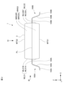
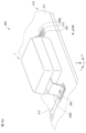
- FIG. 1 is an external perspective view of a multilayer ceramic capacitor according to an embodiment of the present invention
- 2 is a view of the multilayer ceramic capacitor of FIG. 1 as seen from the direction of arrow II.
- 3 is a view of the multilayer ceramic capacitor of FIG. 2 as seen in the direction of arrow III.
- 3 is a view of the multilayer ceramic capacitor of FIG. 2 as seen from the direction of arrow IV.
- FIG. 2 is a diagram corresponding to FIG. 1 and is a virtual perspective view for explaining the internal structure of the multilayer ceramic capacitor.
- 6 is a virtual arrow view of the multilayer ceramic capacitor of FIG. 5 as viewed from the direction of arrow VI.
- FIG. 1 is an external perspective view showing the external appearance of a multilayer ceramic capacitor body before it is covered with an exterior material and before metal terminals are attached; 8 is a cross-sectional view of the multilayer ceramic capacitor body taken along line VIII-VIII in FIG. 7.
- 9 is a cross-sectional view taken along line IX-IX of the multilayer ceramic capacitor body of FIG. 8.
- 9 is a cross-sectional view taken along line XX of the multilayer ceramic capacitor body of FIG. 8.
- FIG. 5 corresponds to FIG. 4 and shows the metal terminals when the exterior material and the multilayer ceramic capacitor body are removed.
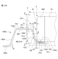
- FIG. 7 is an enlarged view of a portion XIIA of the multilayer ceramic capacitor shown in FIG. 6 .
- FIG. 7 is an enlarged view of a portion XIIB of the multilayer ceramic capacitor shown in FIG. 6.
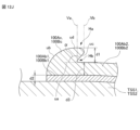
- FIG. 2 is a partial external perspective view of a first metal terminal; 12B is an enlarged view of a portion R1 of the multilayer ceramic capacitor shown in FIG. 12A. 12B is an enlarged view of a portion R2 of the multilayer ceramic capacitor shown in FIG. 12A. FIG. 12B is an enlarged view of a portion R3 of the multilayer ceramic capacitor shown in FIG. 12A. 12E is an enlarged cross-sectional view of a first protrusion located at a portion R4 of the first metal terminal shown in FIG. 12D.
- FIG. 12C is a diagram corresponding to FIG.
- FIG. 12G is an enlarged cross-sectional view showing a first convex portion according to a first modified example.
- FIG. 12C is an enlarged cross-sectional view corresponding to FIG. 12G, showing a low-wettability surface according to a second modified example.
- FIG. 12C is an enlarged cross-sectional view corresponding to FIG. 12G, showing a low-wettability surface according to a third modified example.
- 1 is a diagram of an SEM image of a cross section including a surface of an intermetallic compound.
- FIG. 13B is an elemental mapping image of SEM-EDX based on the SEM image of FIG. 13A.
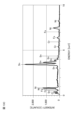
- FIG. 13B is a diagram showing a characteristic X-ray spectrum display at the position of measurement point P1 in FIG. 13A.
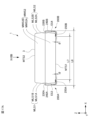
- FIG. 2 is a front view of the metal terminal before being bent.
- FIG. 4 is a diagram showing the opposite surface of the metal terminal before being bent. 4 is a cross-sectional view showing an example of a plurality of protrusions formed on a surface of an intermetallic compound in a first metal terminal.
- FIG. 1 is an external perspective view showing a mounting structure in which a multilayer ceramic capacitor according to an embodiment of the present invention is mounted on a mounting board.
- 16B is a view corresponding to FIG. 6 and is a virtual arrow view of the mounting structure of the multilayer ceramic capacitor of FIG. 16A as viewed from the direction of arrow XVIB.
- FIG. 11 is a diagram showing a fourth modified example of the multilayer ceramic capacitor of the present embodiment, and corresponds to FIG. 2 .
- FIG. 17B is a view of the multilayer ceramic capacitor of FIG. 17A as viewed from the direction of arrow XVIIB.
- FIG. 1 is a diagram showing a multilayer ceramic capacitor having a double structure.
- FIG. 1 is a diagram showing a multilayer ceramic capacitor having a triple structure.
- FIG. 1 is a diagram showing a multilayer ceramic capacitor having a four-row structure.
- FIG. 1 is an external perspective view of the multilayer ceramic capacitor 1.
- FIG. 2 is an arrow view of the multilayer ceramic capacitor 1 in FIG. 1 as viewed from the direction of arrow II.
- FIG. 3 is an arrow view of the multilayer ceramic capacitor 1 in FIG. 2 as viewed from the direction of arrow III.
- FIG. 4 is an arrow view of the multilayer ceramic capacitor 1 in FIG. 2 as viewed from the direction of arrow IV.
- FIG. 5 is a view corresponding to FIG. 1, and is a virtual perspective view for explaining the internal structure of the multilayer ceramic capacitor 1.
- FIG. 6 is a virtual view for explaining the internal structure of the multilayer ceramic capacitor 1, and is a virtual arrow view of the multilayer ceramic capacitor 1 in FIG. 5 as viewed from the direction of arrow VI.
- the multilayer ceramic capacitor 1 has a multilayer ceramic capacitor body 2 as a multilayer ceramic electronic component body, metal terminals 100, and an exterior material 3.
- the multilayer ceramic capacitor body 2 is not shown in Figures 1 to 4 because it is covered by the exterior material 3.
- the multilayer ceramic capacitor body 2 is shown in Figures 5 and 6.
- Fig. 7 is an external perspective view showing the appearance of the multilayer ceramic capacitor body 2 before it is covered with the exterior material 3 and before the metal terminals 100 are attached.
- Fig. 8 is a cross-sectional view of the multilayer ceramic capacitor body 2 taken along line VIII-VIII in Fig. 7.
- Fig. 9 is a cross-sectional view of the multilayer ceramic capacitor body 2 taken along line IX-IX in Fig. 8.
- Fig. 10 is a cross-sectional view of the multilayer ceramic capacitor body 2 taken along line X-X in Fig. 8.
- the multilayer ceramic capacitor body 2 has a laminate 10 and an external electrode 40.
- FIG. 5 to 10 An XYZ orthogonal coordinate system is shown in Figures 5 to 10.
- the length direction L of the multilayer ceramic capacitor body 2 and the laminate 10 corresponds to the X direction.
- the width direction W of the multilayer ceramic capacitor body 2 and the laminate 10 corresponds to the Y direction.
- the height direction T of the multilayer ceramic capacitor body 2 and the laminate 10 corresponds to the Z direction.
- the cross section shown in Figure 8 is also called the LT cross section.
- the cross section shown in Figure 9 is also called the WT cross section.
- the cross section shown in Figure 10 is also called the LW cross section. Note that similar XYZ orthogonal coordinate systems are also shown in Figures 1 to 4, 11, and 16A to 17B.
- the laminate 10 includes a first main surface TS1 and a second main surface TS2 that face the height direction T, a first side surface WS1 and a second side surface WS2 that face the width direction W that is perpendicular to the height direction T, and a first end surface LS1 and a second end surface LS2 that face the length direction L that is perpendicular to the height direction T and the width direction W.
- the laminate 10 has a generally rectangular parallelepiped shape.
- the dimension of the laminate 10 in the length direction L is not necessarily longer than the dimension in the width direction W. It is preferable that the corners and ridges of the laminate 10 are rounded. A corner is a portion where three faces of the laminate intersect, and a ridge is a portion where two faces of the laminate intersect. Incidentally, unevenness may be formed on part or all of the surfaces constituting the laminate 10.
- the dimensions of the laminate 10 are not particularly limited, but if the dimension L of the laminate 10 in the length direction L is taken as the L dimension, it is preferable that the L dimension be 0.2 mm or more and 10 mm or less. If the dimension T of the laminate 10 in the height direction T is taken as the T dimension, it is preferable that the T dimension be 0.1 mm or more and 10 mm or less. If the dimension W of the laminate 10 in the width direction W is taken as the W dimension, it is preferable that the W dimension be 0.1 mm or more and 10 mm or less.
- the inner layer portion 11 includes a plurality of dielectric layers 20 as a plurality of ceramic layers, and a plurality of internal electrode layers 30 as a plurality of internal conductor layers. In the height direction T, the inner layer portion 11 includes the internal electrode layer 30 located closest to the first main surface TS1 to the internal electrode layer 30 located closest to the second main surface TS2. In the inner layer portion 11, the multiple internal electrode layers 30 are arranged opposite each other with the dielectric layer 20 interposed therebetween.
- the inner layer portion 11 is a portion that generates electrostatic capacitance and essentially functions as a capacitor.
- the plurality of dielectric layers 20 are made of a dielectric material.
- the dielectric material may be, for example, a dielectric ceramic containing components such as BaTiO 3 , CaTiO 3 , SrTiO 3 , or CaZrO 3 .
- the dielectric material may also be one in which a subcomponent such as a Mn compound, an Fe compound, a Cr compound, a Co compound, or a Ni compound is added to the main components.
- the thickness of the dielectric layer 20 is preferably 0.5 ⁇ m or more and 72 ⁇ m or less.
- the number of dielectric layers 20 to be stacked is preferably 10 or more and 700 or less.
- the number of dielectric layers 20 is the total number of the dielectric layers in the inner layer portion 11 and the dielectric layers in the first main surface side outer layer portion 12 and the second main surface side outer layer portion 13.
- the multiple internal electrode layers 30 have multiple first internal electrode layers 31 (first internal conductor layers 31) and multiple second internal electrode layers 32 (second internal conductor layers 32).
- the multiple first internal electrode layers 31 are arranged on the multiple dielectric layers 20.
- the multiple second internal electrode layers 32 are arranged on the multiple dielectric layers 20.
- the multiple first internal electrode layers 31 and the multiple second internal electrode layers 32 are arranged alternately in the height direction T of the laminate 10, with the dielectric layers 20 interposed between them.
- the first internal electrode layers 31 and the second internal electrode layers 32 are arranged so as to sandwich the dielectric layers 20 between them.
- the first internal electrode layer 31 has a first opposing portion 31A that faces the second internal electrode layer 32, and a first lead-out portion 31B that is led out from the first opposing portion 31A to the first end surface LS1.
- the first lead-out portion 31B is exposed to the first end surface LS1.
- the second internal electrode layer 32 has a second opposing portion 32A that faces the first internal electrode layer 31, and a second lead-out portion 32B that is led out from the second opposing portion 32A to the second end surface LS2.
- the second lead-out portion 32B is exposed to the second end surface LS2.
- the first opposing portion 31A and the second opposing portion 32A face each other via the dielectric layer 20, forming a capacitance and exhibiting the characteristics of a capacitor.
- the shapes of the first opposing portion 31A and the second opposing portion 32A are not particularly limited, but are preferably rectangular. However, the corners of the rectangular shape may be rounded or the corners of the rectangular shape may be formed at an angle.
- the shapes of the first pull-out portion 31B and the second pull-out portion 32B are not particularly limited, but are preferably rectangular. However, the corners of the rectangular shape may be rounded or the corners of the rectangular shape may be formed at an angle.
- the dimension in the width direction W of the first opposing portion 31A and the dimension in the width direction W of the first pull-out portion 31B may be the same, or one of the dimensions may be smaller.
- the dimension in the width direction W of the second opposing portion 32A and the dimension in the width direction W of the second pull-out portion 32B may be the same, or one of the dimensions may be smaller.
- the first internal electrode layer 31 and the second internal electrode layer 32 are made of an appropriate conductive material, such as a metal such as Ni, Cu, Ag, Pd, or Au, or an alloy containing at least one of these metals. When an alloy is used, the first internal electrode layer 31 and the second internal electrode layer 32 may be made of, for example, an Ag-Pd alloy.
- each of the first internal electrode layer 31 and the second internal electrode layer 32 is preferably, for example, about 0.2 ⁇ m or more and 3.0 ⁇ m or less.
- the total number of the first internal electrode layers 31 and the second internal electrode layers 32 is preferably 5 or more and 350 or less.
- the first main surface side outer layer portion 12 is located on the first main surface TS1 side of the laminate 10.
- the first main surface side outer layer portion 12 is an assembly of dielectric layers 20 as multiple ceramic layers located between the first main surface TS1 and the internal electrode layer 30 closest to the first main surface TS1.
- the first main surface side outer layer portion 12 is formed from multiple dielectric layers 20 located between the first main surface TS1 and the internal electrode layer 30 located closest to the first main surface TS1 side among the multiple internal electrode layers 30.
- the dielectric layer 20 used in the first main surface side outer layer portion 12 may be the same as the dielectric layer 20 used in the internal layer portion 11.
- the second main surface side outer layer portion 13 is located on the second main surface TS2 side of the laminate 10.
- the second main surface side outer layer portion 13 is an assembly of dielectric layers 20 as multiple ceramic layers located between the second main surface TS2 and the internal electrode layer 30 closest to the second main surface TS2.
- the second main surface side outer layer portion 13 is formed from multiple dielectric layers 20 located between the second main surface TS2 and the internal electrode layer 30 located closest to the second main surface TS2 side among the multiple internal electrode layers 30.
- the dielectric layer 20 used in the second main surface side outer layer portion 13 may be the same as the dielectric layer 20 used in the internal layer portion 11.
- the laminate 10 has a plurality of laminated dielectric layers 20 and a plurality of internal electrode layers 30 laminated on the dielectric layers 20.
- the multilayer ceramic capacitor 1 has a laminate 10 in which the dielectric layers 20 and the internal electrode layers 30 are alternately laminated.
- the laminate 10 has an opposing electrode portion 11E.
- the opposing electrode portion 11E is a portion where the first opposing portion 31A of the first internal electrode layer 31 and the second opposing portion 32A of the second internal electrode layer 32 face each other.
- the opposing electrode portion 11E is configured as a part of the inner layer portion 11.
- Figure 8 shows the range in the length direction L of the opposing electrode portion 11E.
- Figure 9 shows the range in the width direction W of the opposing electrode portion 11E.
- Figure 10 shows the range in the width direction W and length direction L of the opposing electrode portion 11E.
- the opposing electrode portion 11E is also called the effective portion of the capacitor.
- the laminate 10 has a side surface outer layer portion.
- the side surface outer layer portion has a first side surface outer layer portion WG1 and a second side surface outer layer portion WG2.
- the first side surface outer layer portion WG1 is a portion including the dielectric layer 20 located between the opposing electrode portion 11E and the first side surface WS1.
- the second side surface outer layer portion WG2 is a portion including the dielectric layer 20 located between the opposing electrode portion 11E and the second side surface WS2.
- Figures 9 and 10 show the range of the width direction W of the first side surface outer layer portion WG1 and the second side surface outer layer portion WG2.
- the first side surface outer layer portion WG1 and the second side surface outer layer portion WG2 are also called W gaps or side gaps.
- the laminate 10 has an end surface side outer layer portion.
- the end surface side outer layer portion has a first end surface side outer layer portion LG1 and a second end surface side outer layer portion LG2.
- the first end surface side outer layer portion LG1 is a portion including the dielectric layer 20 and the first lead portion 31B located between the counter electrode portion 11E and the first end surface LS1.
- the second end surface side outer layer portion LG2 is a portion including the dielectric layer 20 and the second lead portion 32B located between the counter electrode portion 11E and the second end surface LS2.
- FIG. 8 and FIG. 10 the range of the length direction L of the first end surface side outer layer portion LG1 and the second end surface side outer layer portion LG2 is shown.
- the first end surface side outer layer portion LG1 and the second end surface side outer layer portion LG2 are also called L gaps or end gaps.
- the external electrode 40 has a first external electrode 40A arranged on the first end face LS1 side and a second external electrode 40B arranged on the second end face LS2 side.
- the first external electrode 40A may be disposed, for example, extending from the first end face LS1 to a part of the first main surface TS1.
- the cross-sectional shape of the first external electrode 40A may be L-shaped (not shown).
- the portion of the first external electrode 40A that is disposed on the first main surface TS1 is connected to the first metal terminal 100A, which will be described later, via a bonding material.
- the length L1 in the length direction L of the first external electrode 40A provided on the first main surface TS1 is 10% to 40% (e.g., 20 ⁇ m to 4000 ⁇ m) of the L dimension of the laminate.
- the first external electrode 40A is also provided on the second main surface TS2, the first side surface WS1, and the second side surface WS2, it is preferable that the length L1 in the length direction L of the first external electrode 40A provided on these surfaces is also 10% to 40% (e.g., 20 ⁇ m to 4000 ⁇ m) of the L dimension of the laminate.
- the length T1 in the height direction T of the first external electrode 40A provided on this portion is approximately equal to the dimension T of the laminate 10 (e.g., 0.1 mm or more and 10 mm or less).
- the second external electrode 40B is disposed at least on the second end face LS2 side on the first main surface TS1. It is preferable that the second external electrode 40B is disposed at least on the second end face LS2 and a part of the first main surface TS1. In this embodiment, the second external electrode 40B is disposed on the second end face LS2, a part of the first main surface TS1, a part of the second main surface TS2, a part of the first side surface WS1, and a part of the second side surface WS2. In this embodiment, the second external electrode 40B is connected to the second internal electrode layer 32 on the second end face LS2.
- the second external electrode 40B may be disposed, for example, extending from the second end face LS2 to a part of the first main surface TS1.
- the cross-sectional shape of the second external electrode 40B may be L-shaped (not shown).
- the portion of the second external electrode 40B that is disposed on the first main surface TS1 is connected to the second metal terminal 100B, which will be described later, via a bonding material.
- the length L2 in the length direction L of the second external electrode 40B provided on the first main surface TS1 is 10% to 40% (e.g., 20 ⁇ m to 4000 ⁇ m) of the L dimension of the laminate.
- the second external electrode 40B is also provided on the second main surface TS2, the first side surface WS1, and the second side surface WS2, the length L2 in the length direction L of the second external electrode 40B provided on these surfaces is also 10% to 40% (e.g., 20 ⁇ m to 4000 ⁇ m) of the L dimension of the laminate.
- the length W1 in the width direction W of the second external electrode 40B provided on the first main surface TS1 is approximately equal to the dimension W of the laminate 10 (e.g., 0.1 mm or more and 10 mm or less).
- the second external electrode 40B is also provided on the second main surface TS2
- the length W1 in the width direction W of the second external electrode 40B provided on the second main surface TS2 is approximately equal to the dimension W of the laminate 10 (e.g., 0.1 mm or more and 10 mm or less).
- the length T1 in the height direction T of the second external electrode 40B provided on this portion is approximately equal to the dimension T of the laminate 10 (e.g., 0.1 mm or more and 10 mm or less).
- the length L3 of the portion of the surface of the laminate 10 that is exposed from the external electrode 40 in the longitudinal direction L is preferably 20% to 80% (e.g., 40 ⁇ m to 8000 ⁇ m) of the L dimension of the laminate.
- the separation distance L3 between the first external electrode 40A and the second external electrode 40B is preferably 20% to 80% (e.g., 40 ⁇ m to 8000 ⁇ m) of the L dimension of the laminate.
- the first opposing portion 31A of the first internal electrode layer 31 and the second opposing portion 32A of the second internal electrode layer 32 face each other via the dielectric layer 20, forming a capacitance. Therefore, the characteristics of a capacitor are expressed between the first external electrode 40A to which the first internal electrode layer 31 is connected and the second external electrode 40B to which the second internal electrode layer 32 is connected.
- the first external electrode 40A has a first base electrode layer 50A and a first plating layer 60A disposed on the first base electrode layer 50A.
- the second external electrode 40B has a second base electrode layer 50B and a second plating layer 60B disposed on the second base electrode layer 50B.
- the first base electrode layer 50A is disposed on the first end face LS1.
- the first base electrode layer 50A is connected to the first internal electrode layer 31.
- the first base electrode layer 50A is formed extending from the first end face LS1 to a portion of the first main surface TS1 and a portion of the second main surface TS2, as well as a portion of the first side surface WS1 and a portion of the second side surface WS2.
- the second base electrode layer 50B is disposed on the second end face LS2.
- the second base electrode layer 50B is connected to the second internal electrode layer 32.
- the second base electrode layer 50B is formed to extend from the second end face LS2 to a portion of the first main surface TS1 and a portion of the second main surface TS2, as well as a portion of the first side surface WS1 and a portion of the second side surface WS2.
- the first base electrode layer 50A and the second base electrode layer 50B of this embodiment are baked layers.
- the baked layer preferably contains a metal component and either a glass component or a ceramic component, or both.
- the metal component includes at least one selected from, for example, Cu, Ni, Ag, Pd, Ag-Pd alloy, Au, etc.
- the glass component includes at least one selected from, for example, B, Si, Ba, Mg, Al, Li, etc.
- the ceramic component may be the same type of ceramic material as the dielectric layer 20, or a different type of ceramic material.
- the ceramic component includes at least one selected from, for example, BaTiO 3 , CaTiO 3 , (Ba, Ca)TiO 3 , SrTiO 3 , CaZrO 3 , etc.
- the baked layer is, for example, a conductive paste containing glass and metal applied to the laminate and baked.
- the baked layer may be a layer formed by simultaneously baking a laminated chip having an internal electrode layer and a dielectric layer and a conductive paste applied to the laminated chip, or a layer formed by simultaneously baking a laminated chip having an internal electrode layer and a dielectric layer and a conductive paste applied to the laminated chip, and then applying the conductive paste to the laminate and baking it.
- the baked layer may be a multi-layered layer.
- the thickness in the longitudinal direction of the first base electrode layer 50A located on the first end surface LS1 is preferably, for example, about 10 ⁇ m or more and 200 ⁇ m or less at the center in the height direction T and width direction W of the first base electrode layer 50A.
- the thickness in the longitudinal direction of the second base electrode layer 50B located on the second end surface LS2 is preferably, for example, about 10 ⁇ m or more and 200 ⁇ m or less at the center in the height direction T and width direction W of the second base electrode layer 50B.
- the thickness in the height direction of the first base electrode layer 50A provided on this portion is preferably, for example, about 5 ⁇ m or more and 40 ⁇ m or less at the center in the length direction L and width direction W of the first base electrode layer 50A provided on this portion.
- the widthwise thickness of the first base electrode layer 50A provided on this portion is preferably, for example, about 5 ⁇ m or more and 40 ⁇ m or less at the center in the length direction L and height direction T of the first base electrode layer 50A provided on this portion.
- the widthwise thickness of the second base electrode layer 50B provided on this portion is preferably, for example, about 5 ⁇ m or more and 40 ⁇ m or less at the center in the length direction L and height direction T of the second base electrode layer 50B provided on this portion.
- the first base electrode layer 50A and the second base electrode layer 50B are not limited to baked layers, and may be thin film layers.
- the thin film layer is a layer in which metal particles are deposited, formed by a thin film formation method such as sputtering or vapor deposition.
- the thin film layer preferably contains at least one metal selected from the group consisting of Mg, Al, Ti, W, Cr, Cu, Ni, Ag, Co, Mo, and V. This can increase the adhesive strength of the external electrode 40 to the laminate 10.
- the thin film layer may be a single layer, or may be formed of multiple layers. For example, it may be formed of a two-layer structure of a NiCr layer and a NiCu layer.
- the sputter electrode is preferably formed on a part of the first main surface TS1 and a part of the second main surface TS2 of the laminate 10.
- the sputter electrode preferably contains at least one metal selected from, for example, Ni, Cr, Cu, etc.
- the thickness of the sputter electrode is preferably 50 nm or more and 400 nm or less, and more preferably 50 nm or more and 130 nm or less.
- a sputtered electrode may be formed on a part of the first main surface TS1 and a part of the second main surface TS2 of the laminate 10, while a baked layer may be formed on the first end face LS1 and the second end face LS2.
- a plating layer (described later) may be formed directly on the laminate 10 without forming a base electrode layer on the first end face LS1 and the second end face LS2.
- the baked layer may be arranged to extend not only on the first end face LS1 and the second end face LS2, but also on a part of the first main surface TS1 and a part of the second main surface TS2.
- the sputtered electrode may be arranged so as to overlap the baked layer.
- the first plating layer 60A is arranged to cover the first base electrode layer 50A.
- the first plating layer 60A is disposed so as to cover the first base electrode layer 50A.
- the first plating layer 60A has a first Ni plating layer 61A and a first Sn plating layer 62A located on the first Ni plating layer 61A.
- the Ni plating layer prevents the first base electrode layer 50A and the second base electrode layer 50B from being eroded by the solder serving as the bonding material 5 that bonds the multilayer ceramic capacitor body 2 and the metal terminal 100.
- the Sn plating layer also improves the wettability of the solder serving as the bonding material 5 that bonds the multilayer ceramic capacitor body 2 and the metal terminal 100. This facilitates bonding of the multilayer ceramic capacitor body 2 and the metal terminal 100.
- the first plating layer 60A and the second plating layer 60B each have a two-layer structure of a Ni plating layer and a Sn plating layer, it is preferable that the thickness of each of the Ni plating layer and the Sn plating layer is 1 ⁇ m or more and 15 ⁇ m or less.
- the metal constituting the conductive particles may be Ag, Cu, Ni, Sn, Bi, or an alloy containing these.
- the conductive particles preferably contain Ag.
- the conductive particles are, for example, Ag metal powder. Ag has the lowest resistivity of all metals, making it suitable as an electrode material. In addition, Ag is a precious metal, so it is resistant to oxidation and has high weather resistance. Therefore, Ag metal powder is suitable as a conductive particle.
- the conductive particles may also be metal powder with an Ag coating on the surface.
- the metal powder is preferably a powder of Cu, Ni, Sn, Bi or an alloy thereof. In order to make the base metal less expensive while maintaining the properties of Ag, it is preferable to use Ag-coated metal powder.
- the conductive particles may be Cu or Ni that has been subjected to an anti-oxidation treatment.
- the conductive particles may also be metal powder with a surface coating of Sn, Ni, or Cu.
- the metal powder is Ag, Cu, Ni, Sn, Bi, or an alloy powder of these.
- the shape of the conductive particles is not particularly limited.
- the conductive particles may be spherical, flat, or the like, but it is preferable to use a mixture of spherical metal powder and flat metal powder.
- the conductive particles contained in the conductive resin layer are primarily responsible for ensuring the electrical conductivity of the conductive resin layer. Specifically, when multiple conductive particles come into contact with each other, a conductive path is formed inside the conductive resin layer.
- the resin constituting the conductive resin layer may contain at least one selected from various known thermosetting resins, such as epoxy resin, phenol resin, urethane resin, silicone resin, and polyimide resin.
- thermosetting resins such as epoxy resin, phenol resin, urethane resin, silicone resin, and polyimide resin.
- epoxy resin which has excellent heat resistance, moisture resistance, and adhesion, is one of the most suitable resins.
- the resin of the conductive resin layer contains a hardener in addition to the thermosetting resin.
- the hardener of the epoxy resin may be various known compounds such as phenol-based, amine-based, acid anhydride-based, imidazole-based, active ester-based, and amide-imide-based compounds.
- the conductive resin layer may be formed of multiple layers.
- the thickness of the thickest part of the conductive resin layer is preferably 10 ⁇ m or more and 150 ⁇ m or less.
- the multilayer ceramic capacitor 1 may have a configuration including plating layers that are directly and electrically connected to the first internal electrode layer 31 and the second internal electrode layer 32.
- the plating layers may be formed after a catalyst is disposed on the surface of the laminate 10 as a pretreatment.
- each plating layer that is placed without providing an underlying electrode layer is preferably 2 ⁇ m or more and 10 ⁇ m or less. It is preferable that the plating layer does not contain glass.
- the metal ratio per unit volume of the plating layer is preferably 99 volume % or more.
- the thickness of the base electrode layer can be reduced. Therefore, the dimension in the height direction T of the multilayer ceramic capacitor body 2 can be reduced by the amount of the reduction in the thickness of the base electrode layer, thereby making it possible to reduce the height of the multilayer ceramic capacitor body 2.
- the thickness of the dielectric layer 20 sandwiched between the first internal electrode layer 31 and the second internal electrode layer 32 can be increased by the amount of the reduction in the thickness of the base electrode layer, thereby improving the thickness of the element. In this way, by forming the plating layer directly on the laminate 10, the design freedom of the multilayer ceramic capacitor can be improved.
- L dimension lengthwise dimension of the multilayer ceramic capacitor body 2 including the laminate 10 and the external electrodes 40
- L dimension is 0.2 mm or more and 10 mm or less.
- T dimension is 0.1 mm or more and 10 mm or less.
- W dimension is 0.1 mm or more and 10 mm or less.
- the first surface S1 on the first end face LS1 side of the multilayer ceramic capacitor body 2 is formed by the surface of the first external electrode 40A arranged on the first end face LS1.
- the second surface S2 on the second end face LS2 side of the multilayer ceramic capacitor body 2 is formed by the surface of the second external electrode 40B arranged on the second end face LS2.
- the metal terminal 100 has a first metal terminal 100A and a second metal terminal 100B.
- the first metal terminal 100A and the second metal terminal 100B are metal terminals mounted on the mounting surface of a mounting board (see mounting board 310 in Figures 16A and 16B) to be described later on, on which the multilayer ceramic capacitor 1 is to be mounted.
- the first metal terminal 100A and the second metal terminal 100B are, for example, plate-shaped lead frames.
- the first main surface TS1 of the laminate 10 is the surface opposite to the mounting surface of the mounting board on which the multilayer ceramic capacitor 1 is to be mounted.
- the first metal terminal 100A has a first joint 110A facing the first main surface TS1 and connected to the first external electrode 40A, a first rising portion 120A connected to the first joint 110A, extending away from the mounting surface of the mounting board, and facing the first end surface LS1, a first extension portion 130A connected to the first rising portion 120A and extending in the length direction L away from the multilayer ceramic capacitor body 2, a first falling portion 140A connected to the first extension portion 130A and extending toward the mounting surface side of the mounting board, and a first mounting portion 150A connected to the first falling portion 140A and extending in a direction along the mounting surface of the mounting board.
- a gap portion G exists between the first rising portion 120A and the first surface S1 on the first end surface LS1 side of the multilayer ceramic capacitor body 2. Details about the first metal terminal 100A will be described later.
- the second metal terminal 100B has a second joint 110B facing the first main surface TS1 and connected to the second external electrode 40B, a second rising portion 120B connected to the second joint 110B, extending away from the mounting surface of the mounting board, and facing the second end face LS2, a second extension portion 130B connected to the second rising portion 120B and extending in the length direction L away from the multilayer ceramic capacitor body 2, a second falling portion 140B connected to the second extension portion 130B and extending toward the mounting surface side of the mounting board, and a second mounting portion 150B connected to the second falling portion 140B and extending in a direction along the mounting surface of the mounting board.
- a gap portion G exists between the second rising portion 120B and the second surface S2 on the second end face LS2 side of the multilayer ceramic capacitor body 2. Details about the second metal terminal 100B will be described later.
- first falling portion 140A and the second falling portion 140B extend toward the mounting surface of the mounting board to an extent that allows a gap to be provided between the exterior material 3 of the multilayer ceramic capacitor 1 and the mounting surface of the mounting board.
- the distance between the mounting substrate and the multilayer ceramic electronic component body 2 can be increased, which has the effect of alleviating stress from the mounting substrate.
- the thickness of the exterior material 3 provided on the mounting substrate side can be increased, ensuring insulation.
- the separation distance L4 between the first mounting portion 150A of the first metal terminal 100A and the second mounting portion 150B of the second metal terminal 100B is longer than the separation distance L3 between the first external electrode 40A and the second external electrode 40B of the multilayer ceramic capacitor body 2.
- the bonding material 5 bonds the multilayer ceramic capacitor body 2 to the metal terminal 100.
- the bonding material 5 has a first bonding material 5A and a second bonding material 5B.
- the first metal terminal 100A is connected to the first external electrode 40A via a first bonding material 5A.
- the second metal terminal 100B is connected to the second external electrode 40B via a second bonding material 5B.
- the bonding material 5 is preferably a solder.
- it may be a Pb-free solder.
- a lead-free solder such as Sn-Sb, Sn-Ag-Cu, Sn-Cu, or Sn-Bi is preferable.
- Sn-10Sb to Sn-15Sb solder can be used.
- the exterior material 3 will be explained using Figures 1 to 6.
- the exterior material 3 includes a first main surface MTS1 and a second main surface MTS2 facing the height direction T, a first side surface MWS1 and a second side surface MWS2 facing the width direction W perpendicular to the height direction T, and a first end surface MLS1 and a second end surface MLS2 facing the length direction L perpendicular to the height direction T and the width direction W.
- the first end surface MLS1 of the exterior material 3 is the surface of the exterior material 3 facing the first end surface LS1 of the laminate 10.
- the second end surface MLS2 of the exterior material 3 is the surface of the exterior material 3 facing the second end surface LS2 of the laminate 10.
- the first side surface MWS1, the second side surface MWS2, the first end surface MLS1, and the second end surface MLS2 of the exterior material 3 have a parting line PL in the center in the height direction T.
- the parting line PL is a line that corresponds to the parting surface of the mold used when molding the exterior material 3.
- the surface of the exterior material 3 has a draft angle with the parting line PL as the boundary.
- the first side surface MWS1 of the exterior material 3 has a surface MWS1A on the first main surface side and a surface MWS1B on the second main surface side.
- the second side surface MWS2 of the exterior material 3 has a surface MWS2A on the first main surface side and a surface MWS2B on the second main surface side.
- the first end surface MLS1 of the exterior material 3 has a surface MLS1A on the first main surface side and a surface MLS1B on the second main surface side.
- the second end surface MLS2 of the exterior material 3 has a surface MLS2A on the first main surface side and a surface MLS2B on the second main surface side.
- Each of the surfaces MWS1A, MWS2A, MLS1A, and MLS2A on the first main surface side has a draft angle such that the cross-sectional area of the LW cross section of the exterior material 3 decreases as it approaches the first main surface TS1 from the parting line PL.
- Each of the surfaces MWS1B, MWS2B, MLS1B, and MLS2B on the second main surface side has a draft angle such that the cross-sectional area of the LW cross section of the exterior material 3 decreases as it approaches the second main surface TS2 from the parting line PL.
- the exterior material 3 covers the multilayer ceramic capacitor body 2, the bonding material 5 that connects the multilayer ceramic capacitor body 2 and the metal terminal 100, and a portion of the metal terminal 100. Specifically, the exterior material 3 is arranged to cover the entire multilayer ceramic capacitor body 2, the entire first bonding material 5A and the second bonding material 5B, a portion of the first metal terminal 100A, and a portion of the second metal terminal 100B.
- the exterior material 3 is arranged to cover the entire first joint portion 110A, the entire first rising portion 120A, and at least a part of the first extension portion 130A of the first metal terminal 100A. Also, the exterior material 3 is arranged to cover the entire second joint portion 110B, the entire second rising portion 120B, and at least a part of the second extension portion 130B of the second metal terminal 100B.
- the second main surface MTS2 of the exterior material 3 is preferably configured to be planar with a predetermined degree of flatness. This makes it possible to prevent poor adhesion of the mounter of the mounting machine used when mounting the multilayer ceramic capacitor 1 on the mounting board. This makes it possible to reliably mount the multilayer ceramic capacitor 1 on the mounting board. As a result, it becomes possible to suppress the occurrence of mounting defects.
- the minimum distance from the second side surface MWS2 of the exterior material 3 to the surface of the multilayer ceramic capacitor body 2 is 100 ⁇ m or more and 4000 ⁇ m or less. It is preferable that the minimum distance from the first end surface MLS1 of the exterior material 3 to the surface of the multilayer ceramic capacitor body 2 is 300 ⁇ m or more and 5000 ⁇ m or less. The minimum distance from the second end face MLS2 of the exterior material 3 to the surface of the multilayer ceramic capacitor body 2 is preferably 300 ⁇ m or more and 5000 ⁇ m or less.
- the exterior material 3 is preferably made of resin.
- the exterior material 3 may be formed by molding an engineering plastic by a transfer molding method, an injection molding method, or the like.
- the material of the exterior material 3 is preferably made of a thermosetting epoxy resin. This ensures adhesion between the exterior material 3 and the multilayer ceramic capacitor body 2 and the metal terminals 100, and improves the withstand voltage and moisture resistance.
- the exterior material 3 may be formed, for example, by painting with a liquid or powdered silicone-based or epoxy-based resin.
- the exterior material 3 covers a wide range of the conductor metal parts, such as the external electrode 40 and the metal terminal 100, thereby ensuring the insulating surface distance (creepage distance) between the conductors.
- the risk of surface discharge can be avoided.
- the shape of the exterior material 3 is not particularly limited. For example, it may be a truncated pyramid, such as a pyramid.
- the shape of the corners of the exterior material 3 is not particularly limited and may be rounded.
- Figures 12A to 12F will be used to explain the structure around the joint between the external electrode 40 of the multilayer ceramic capacitor body 2 and the metal terminal 100, as well as the details of the metal terminal 100.
- FIG. 12A is an enlarged view of portion XIIA of the multilayer ceramic capacitor 1 shown in FIG. 6, and is a diagram for explaining the configuration around the joint between the first external electrode 40A and the first metal terminal 100A, and the details of the first metal terminal 100A.
- FIG. 12B is an enlarged view of portion XIIB of the multilayer ceramic capacitor 1 shown in FIG. 6, and is a diagram for explaining the configuration around the joint between the second external electrode 40B and the second metal terminal 100B, and the details of the second metal terminal 100B.
- FIG. 12C is a partial external perspective view of the first metal terminal 100A.
- a gap G exists between the first rising portion 120A of the first metal terminal 100A and the first surface S1 on the first end face LS1 side of the multilayer ceramic capacitor body 2, and the exterior material 3 is filled in the gap G.
- the first surface S1 is formed by the surface of the first external electrode 40A arranged on the first end face LS1. That is, in this embodiment, a gap G exists between the first rising portion 120A and the first surface S1 of the first external electrode 40A arranged on the first end face LS1, and the exterior material 3 is filled in the gap G.
- the average distance in the length direction L of this gap G is preferably 50 ⁇ m or more and 1500 ⁇ m or less.
- the exterior material 3 can be appropriately filled into the gap G, which can prevent problems such as solder splash during reflow when mounting on the board.
- the first rising portion 120A is inclined away from the first surface S1 on the first end face LS1 side of the multilayer ceramic capacitor body 2 as it moves from the connection portion with the first joint portion 110A to the connection portion with the first extension portion 130A.
- the distance in the length direction L of the gap G becomes longer as it moves from a position closer to the mounting surface of the mounting board to a position farther away.
- the distance G2 in the length direction L at a position farther away from the mounting surface of the gap G is longer than the distance G1 in the length direction L at a position closer to the mounting surface of the gap G.
- the angle ⁇ between the first rising portion 120A and the first surface S1 on the first end face LS1 side of the multilayer ceramic capacitor body 2 is preferably 1° or more and 40° or less.
- the surface MLS1A on the first main surface side that forms the first end surface MLS1 of the exterior material 3 and is closer to the mounting surface side than the portion where the first extension portion 130A protrudes constitutes the first inclined surface of the exterior material 3.
- the first inclined surface MLS1A is inclined so as to move away from the first surface S1 of the multilayer ceramic capacitor body 2 as it moves from a position closer to the mounting surface to a position farther away.
- the draft angle ⁇ of this first inclined surface MLS1A is preferably 1° or more and 20° or less.
- the angle between the first rising portion 120A and the first inclined surface MLS1A is preferably 30° or less.
- the distance from the first inclined surface MLS1A of the exterior material 3 to the first rising portion 120A of the first metal terminal 100A can be made approximately constant. This ensures strength around the first rising portion 120A, which is more susceptible to force.
- the exterior material 3 can be appropriately filled into the gap G, which can prevent problems such as solder splash during reflow when mounting on the board.
- the second rising portion 120B is inclined away from the second surface S2 on the second end face LS2 side of the multilayer ceramic capacitor body 2 as it moves from the connection portion with the second joint portion 110B to the connection portion with the second extension portion 130B.
- the distance in the length direction L of the gap G becomes longer as it moves from a position closer to the mounting surface of the mounting board to a position farther away.
- the distance G2 in the length direction L at a position farther away from the mounting surface of the gap G is longer than the distance G1 in the length direction L at a position closer to the mounting surface of the gap G.
- the angle ⁇ between the second rising portion 120B and the second surface S2 on the second end face LS2 side of the multilayer ceramic capacitor body 2 is preferably 1° or more and 40° or less.
- the surface MLS2A on the first main surface side that forms the second end surface MLS2 of the exterior material 3 and is closer to the mounting surface than the portion where the second extension portion 130B protrudes constitutes the second inclined surface of the exterior material 3.
- the second inclined surface MLS2A is inclined so as to move away from the second surface S2 of the multilayer ceramic capacitor body 2 as it moves from a position closer to the mounting surface to a position farther away.
- the draft angle ⁇ of this second inclined surface MLS2A is preferably 1° or more and 20° or less.
- the angle between the second rising portion 120B and the second inclined surface MLS2A is preferably 30° or less.
- the distance from the second inclined surface MLS2A of the exterior material 3 to the second rising portion 120B of the second metal terminal 100B can be made approximately constant. This ensures strength around the second rising portion 120B, which is more susceptible to force.
- the average distance in the length direction L of the measurement target part is measured by the following method.
- the multilayer ceramic capacitor 1 is cross-polished to a position of about half the W dimension to expose a specific LT cross section where the cross section of the metal terminal 100 can be confirmed.
- the LT cross section of the multilayer ceramic capacitor 1 exposed by polishing is then observed with an SEM.
- 10 lines extending in the length direction L are drawn at equal intervals in the height T direction in the measurement target part, and the average distance of these 10 lines is taken as the average distance in the length direction L of the measurement target part in this embodiment.
- FIG. 12C is an external perspective view showing a portion of the external appearance of the first metal terminal 100A, representing the metal terminals 100.
- the first metal terminal 100A and the second metal terminal 100B are generally plane-symmetrical with respect to the WT cross section at the center of the longitudinal direction L of the multilayer ceramic capacitor 1. Therefore, an external perspective view (not shown) of the second metal terminal 100B is basically the same as the external perspective view of the first metal terminal 100A.
- the first metal terminal 100A has a first notch 160A, a first opening 170A, and a third notch 180A.
- the first notch 160A extends continuously from the end of the first joint 110A to a position midway through the first rising portion 120A.
- the resin constituting the exterior material 3 flows through the first notch 160A, making it easier to fill the gap G with resin.
- the resin constituting the exterior material 3 flows through the first notch 160A, making it easier to fill the gap G with resin.
- the resin constituting the exterior material 3 in the first notch 160A by arranging the resin constituting the exterior material 3 in the first notch 160A, the resin on one side of the first rising portion 120A of the first metal terminal 100A and the resin on the other side are connected by the resin in the first notch 160A, making the structure stronger.
- the cut-out portion of the first notch 160A extends to a position midway through the first rising portion 120A, so the strength of the first metal terminal 100A is ensured.
- the first rising portion 120A in this embodiment is inclined as described above, for example, when molding the exterior material 3, the resin that constitutes the exterior material 3 easily enters
- the rising height T3 in the height direction T of the first notch 160A is less than half the rising height T2 in the height direction T of the first rising portion 120A. This makes it possible to ensure the strength of the first metal terminal 100A while ensuring the flowability of the resin that constitutes the exterior material 3, for example, when molding the exterior material 3.
- the first joint portion 110A has a first joint piece 111A on the first side surface WS1 side and a second joint piece 112A on the second side surface WS2 side, which are separated by a first cutout 160A.
- the first opening 170A is disposed in the first extension 130A.
- the flowability of the resin constituting the exterior material 3 can be further increased, for example, when molding the exterior material 3.
- the resin constituting the exterior material 3 by disposing the resin constituting the exterior material 3 in the first opening 170A, the resin on one side of the first extension 130A of the first metal terminal 100A and the resin on the other side are connected by the resin in the first opening 170A, making the structure stronger.
- the same material constituting the exterior material 3 is disposed in the portion of the first notch 160A formed in the first rising portion 120A and the first opening 170A. This makes the structure of the multilayer ceramic capacitor 1 stronger.
- the length W4 of the width direction W of the first cutout 160A may be approximately the same as the length W5 of the width direction W of the first opening 170A.
- the rising height T3 of the first cutout 160A in the height direction T may be approximately the same as the length L6 of the length direction L of the first opening 170A.
- the area of the first cutout 160A formed in the first rising portion 120A may be within a range of 50% to 200% of the area of the first opening 170A. This allows the resin that constitutes the exterior material 3 to flow in a balanced manner, for example, when the exterior material 3 is molded.
- the second metal terminal 100B has a second notch 160B, a second opening 170B, and a fourth notch 180B.
- the second notch 160B extends continuously from the end of the second joint 110B to a position midway along the second rising portion 120B.
- the resin constituting the exterior material 3 flows through the second notch 160B, making it easier to fill the gap G with resin.
- the resin constituting the exterior material 3 flows through the second notch 160B, making it easier to fill the gap G with resin.
- the resin constituting the exterior material 3 in the second notch 160B by arranging the resin constituting the exterior material 3 in the second notch 160B, the resin on one side of the second rising portion 120B of the second metal terminal 100B and the resin on the other side are connected by the resin in the second notch 160B, making the structure stronger.
- the cut-out portion of the second notch 160B extends to a position midway along the second rising portion 120B, ensuring the strength of the second metal terminal 100B.
- the second rising portion 120B in this embodiment is inclined as described above, for example, when molding the exterior material 3, the resin that constitutes the exterior material 3 easily enters the gap
- the rising height T3 of the second cutout 160B in the height direction T is preferably less than half the rising height T2 of the second rising portion 120B in the height direction T. This ensures the flowability of the resin that constitutes the exterior material 3 while also ensuring the strength of the second metal terminal 100B, for example, when molding the exterior material 3.
- the second joint portion 110B has a third joint piece 111B on the first side surface WS1 side and a fourth joint piece 112B on the second side surface WS2 side, which are separated by the second notch 160B.
- the second opening 170B is disposed in the second extension 130B.
- the flowability of the resin constituting the exterior material 3 can be further increased, for example, when molding the exterior material 3.
- the resin constituting the exterior material 3 in the second opening 170B, the resin on one side of the second extension 130B of the second metal terminal 100B and the resin on the other side are connected by the resin in the second opening 170B, making the structure stronger.
- the same material constituting the exterior material 3 is disposed in the part of the second notch 160B formed in the second rising portion 120B and the second opening 170B. This makes the structure of the multilayer ceramic capacitor 1 stronger.
- the fourth notch 180B extends continuously from the end of the second mounting portion 150B to a position midway along the second falling portion 140B.
- the widthwise length W2 of the second bonding portion 110B of the second metal terminal 100B is longer than the widthwise length W3 of the second rising portion 120B. This allows a wide bonding area between the second external electrode 40B and the second metal terminal 100B by the second bonding material 5B to be secured. In particular, even when the second notch 160B is provided as described above, a wide bonding area between the second external electrode 40B and the second metal terminal 100B by the second bonding material 5B can be secured.
- the length W4 in the width direction W of the second cutout 160B may be approximately the same as the length W5 in the width direction W of the second opening 170B.
- the rising height T3 in the height direction T of the second cutout 160B may be approximately the same as the length L6 in the length direction L of the second opening 170B.
- the area of the second cutout 160B formed in the second rising portion 120B may be within a range of 50% to 200% of the area of the second opening 170B. This allows the resin that constitutes the exterior material 3 to flow in a balanced manner, for example, when the exterior material 3 is molded.
- the first mounting portion 150A may extend parallel to the mounting surface along the mounting surface, but may extend at an incline away from the mounting surface as it approaches the connection with the first falling portion 140A.
- the second mounting portion 150B may extend parallel to the mounting surface along the mounting surface, but may extend at an incline away from the mounting surface as it approaches the connection with the second falling portion 140B. This allows the bonding material to be drawn into this portion when mounting the multilayer ceramic capacitor 1 to the mounting board, increasing the mounting strength.
- the inclination angle ⁇ is preferably 1° or more and 10° or less.
- L dimension the lengthwise dimension of the multilayer ceramic capacitor 1 including the exterior material 3 and the metal terminals 100 is taken as L dimension, then it is preferable that L dimension is 3.2 mm or more and 20 mm or less. If the dimension in the stacking direction of the multilayer ceramic capacitor 1 is taken as T dimension, then it is preferable that T dimension is 1.0 mm or more and 10 mm or less. If the widthwise dimension of the multilayer ceramic capacitor 1 is taken as W dimension, then it is preferable that W dimension is 1.5 mm or more and 20 mm or less.
- Figure 12D is an enlarged view of the R1 portion of the first metal terminal 100A of the multilayer ceramic capacitor 1 shown in Figure 12A.
- Figure 12E is an enlarged view of the R2 portion of the first metal terminal 100A of the multilayer ceramic capacitor 1 shown in Figure 12A.
- Figure 12F is an enlarged view of the R3 portion of the first metal terminal 100A of the multilayer ceramic capacitor 1 shown in Figure 12A.
- the first metal terminal 100A and the second metal terminal 100B are roughly plane-symmetrical with respect to the WT cross section at the center of the longitudinal direction L of the multilayer ceramic capacitor 1. Therefore, the enlarged view of the second metal terminal 100B has the same shape as the enlarged view of the first metal terminal 100A, and is symmetrical on the left and right sides of the paper.
- the first metal terminal 100A of this embodiment has a first bonding surface 110A1 bonded to the first bonding material 5A and a first contact surface CS1 in contact with the outer casing material 3, and the first contact surface CS1 in contact with the outer casing material 3 has a surface of a first outermost surface plating film 100Ab2 as a first outermost surface metal film, and surfaces E1a, E1b, E1c of a first intermetallic compound 100Ab3 as a first low-wettability surface having lower wettability than the surface of the first outermost surface plating film 100Ab2.
- the second metal terminal 100B has a second bonding surface 110B1 that is bonded to the second bonding material 5B and a second contact surface CS2 that is in contact with the exterior material 3, and the second contact surface CS2 that is in contact with the exterior material 3 has a surface of a second outermost surface plating film 100Bb2 as a second outermost surface metal film, and surfaces E2a, E2b, and E2c of a second intermetallic compound 100Bb3 as a second low-wettability surface that has lower wettability than the surface of the second outermost surface plating film 100Bb2. Details of this will be described below.
- the first metal terminal 100A is a plate-like member including a first front surface FS1 as a first surface on the first bonding surface 110A1 side to which the first external electrode 40A is bonded, a first opposite surface BS1 as a first back surface that is the surface opposite to the first front surface FS1, and a first terminal side surface TSS1 connecting the first front surface FS1 and the first opposite surface BS1.
- the first bonding portion 110A of the first metal terminal 100A has a first bonding surface 110A1 that is bonded to the first bonding material 5A on the first front surface FS1.
- the portion of the surface of the first metal terminal 100A that is embedded in the exterior material 3, excluding the first bonding surface 110A1, is composed of a first contact surface CS1 that is in contact with the exterior material 3.
- the first metal terminal 100A has a first bonding surface 110A1 that is bonded to the first bonding material 5A, and a first contact surface CS1 that is in contact with the exterior material 3.
- the second metal terminal 100B is a plate-like member including a second front surface FS2 as a second surface on the second bonding surface 110B1 side to which the second external electrode 40B is bonded, a second opposite surface BS2 as a second back surface that is the surface opposite to the second front surface FS2, and a second terminal side surface TSS2 connecting the second front surface FS2 and the second opposite surface BS2.
- the second bonding portion 110B of the second metal terminal 100B has a second bonding surface 110B1 that is bonded to the second bonding material 5B on the second front surface FS2.
- the portion of the surface of the second metal terminal 100B that is embedded in the exterior material 3, excluding the second bonding surface 110B1, is composed of a second contact surface CS2 that is in contact with the exterior material 3.
- the second metal terminal 100B has a second bonding surface 110B1 that is bonded to the second bonding material 5B, and a second contact surface CS2 that is in contact with the exterior material 3.
- the first metal terminal 100A includes a first base material 100Aa that constitutes the terminal body, and a first plating film 100Ab formed on the surface of the first base material 100Aa.
- the first plating film 100Ab of the first metal terminal 100A is disposed at least on the portion of the first bonding portion 110A where the first bonding material 5A is disposed, and on the portion of the first mounting portion 150A that faces the mounting surface of the mounting board.
- the second metal terminal 100B includes a second base material 100Ba that constitutes the terminal body, and a second plating film 100Bb formed on the surface of the second base material 100Ba.
- the second plating film 100Bb of the second metal terminal 100B is disposed at least on the portion of the second bonding portion 110B where the second bonding material 5B is disposed, and on the portion of the second mounting portion 150B that faces the mounting surface of the mounting board.
- the plating film preferably has an outermost surface plating film as an upper layer plating film disposed on the outermost surface of the plating film, and a lower layer plating film as a base plating film disposed below the outermost surface plating film.
- the plating film may have a two-layer structure in which the outermost surface plating film is formed on the lower layer plating film.
- the first plating film 100Ab of this embodiment includes a first outermost surface plating film 100Ab2 constituting the first outermost surface metal film, and a first lower layer plating film 100Ab1 disposed below the first outermost surface plating film 100Ab2.
- the first plating film 100Ab of this embodiment includes a first lower layer plating film 100Ab1 as a base plating film covering the surface of the first base material 100Aa, and a first outermost surface plating film 100Ab2 as an upper layer plating film covering the surface of the first lower layer plating film 100Ab1.
- the first outermost surface plating film 100Ab2 includes at least the outermost surface portion of the first plating film 100Ab.
- the second plating film 100Bb of this embodiment includes a second outermost surface plating film 100Bb2 constituting the second outermost surface metal film, and a second lower layer plating film 100Bb1 disposed below the second outermost surface plating film 100Bb2.
- the second plating film 100Bb of this embodiment includes a second lower layer plating film 100Bb1 as a base plating film covering the surface of the second base material 100Ba, and a second outermost surface plating film 100Bb2 as an upper layer plating film covering the surface of the second lower layer plating film 100Bb1.
- the second outermost surface plating film 100Bb2 includes at least the outermost surface portion of the second plating film 100Bb.
- the outermost surface plating film has a surface that is more wettable to solder than the surface of the base metal of the terminal body. In addition, in the plating film structure, the outermost surface plating film has a surface that is more wettable to solder than the surface of the lower layer plating film. In addition, in the plating film structure, the outermost surface plating film has a surface that is more wettable to solder than the surface of the intermetallic compound described below.
- the first contact surface CS1 of the first metal terminal 100A which is in contact with the exterior material 3, comprises a surface of the first outermost surface plating film 100Ab2 as the first outermost surface metal film, and surfaces E1a, E1b, and E1c of the first intermetallic compound 100Ab3 as a first low-wettability surface that has lower solder wettability than the first outermost surface plating film 100Ab2.
- the first intermetallic compound 100Ab3 may be arranged in a layered form as a first intermetallic compound layer on the first lower layer plating film 100Ab1.
- the first intermetallic compound 100Ab3 is composed of an intermetallic compound between the metal constituting the first outermost surface plating film 100Ab2 and the metal constituting the first lower layer plating film 100Ab1.
- the second contact surface CS2 of the second metal terminal 100B which is in contact with the exterior material 3, comprises a surface of the second outermost surface plating film 100Bb2 as the second outermost surface metal film, and surfaces E2a, E2b, and E2c of the second intermetallic compound 100Bb3 as a second low-wettability surface that has lower solder wettability than the second outermost surface plating film 100Bb2.
- the second intermetallic compound 100Bb3 may be arranged in a layered form as a second intermetallic compound layer on the second lower layer plating film 100Bb1.
- the second intermetallic compound 100Bb3 is composed of an intermetallic compound between the metal constituting the second outermost surface plating film 100Bb2 and the metal constituting the second lower layer plating film 100Bb1.
- the lower layer plating film is preferably made of Ni, Fe, Cu, Ag, Cr, or an alloy containing one or more of these metals as a main component. More preferably, the lower layer plating film is made of Ni, Fe, Cr, or an alloy containing one or more of these metals as a main component.
- the heat resistance of the metal terminal can be improved by forming the lower plating film from high-melting point Ni, Fe, Cr, or an alloy containing one or more of these metals as its main component.
- the first lower layer plating film 100Ab1 is a Ni plating film.
- the thickness of the first lower layer plating film 100Ab1 is preferably about 0.2 ⁇ m or more and 5.0 ⁇ m or less.
- the second lower layer plating film 100Bb1 is a Ni plating film.
- the thickness of the second lower layer plating film 100Bb1 is preferably about 0.2 ⁇ m or more and 5.0 ⁇ m or less.
- the outermost surface plating film is preferably made of Sn, Ag, Au, or an alloy containing one or more of these metals as a main component. More preferably, the outermost surface plating film is made of Sn or an alloy containing Sn as a main component. By forming the outermost surface plating film from Sn or an alloy containing Sn as a main component, the solderability between the external electrode and the metal terminal can be improved.
- the first outermost surface plating film 100Ab2 is a Sn plating film.
- the thickness of the first outermost surface plating film 100Ab2 is preferably about 1.0 ⁇ m or more and 5.0 ⁇ m or less.
- the second outermost surface plating film 100Bb2 is a Sn plating film.
- the thickness of the second outermost surface plating film 100Bb2 is preferably about 1.0 ⁇ m or more and 5.0 ⁇ m or less.
- the first intermetallic compound 100Ab3 and the second intermetallic compound 100Bb3 are intermetallic compounds of Ni and Sn. That is, in this embodiment, the first outermost surface plating film 100Ab2 and the second outermost surface plating film 100Bb2 are Sn plating films, the first lower layer plating film 100Ab1 and the second lower layer plating film 100Bb1 are Ni plating films, and the surfaces E1a, E1b, and E1c of the first intermetallic compound 100Ab3 and the surfaces E2a, E2b, and E2c of the second intermetallic compound 100Bb3 are composed of an intermetallic compound of Ni and Sn.
- An example of the intermetallic compound of Ni and Sn is Ni 3 Sn 4. However, the intermetallic compound of Ni and Sn is not limited to this.
- the intermetallic compound may be formed by forming two or more layers of plating film on the terminal body and then subjecting the plating film to heat treatment.
- the laminated structure of Ni plating film and Sn plating film is subjected to heat treatment by laser irradiation to form an intermetallic compound of Ni and Sn.
- the laser irradiation conditions are adjusted to a low output so that the Sn plating film as the outermost surface plating film is not evaporated and removed.
- the terminal body is preferably made of Ni, Fe, Cu, Ag, Cr, or an alloy containing one or more of these metals as a main component.
- the base metal of the terminal body can be an Fe-42Ni alloy, an Fe-18Cr alloy, or a Cu-8Sn alloy.
- the base metal of the terminal body can be oxygen-free copper or a Cu-based alloy, which has high thermal conductivity. In this way, by using a copper-based material with good thermal conductivity for the terminal body, it is possible to achieve low ESR and low thermal resistance.
- the base metal of the terminal body can be stainless steel or aluminum, which has low solder wettability. At least the surface of the base metal of the terminal body has a surface with lower solder wettability than the plating film on the outermost surface.
- the thickness of the terminal body is preferably about 0.05 mm to 0.5 mm.
- the first metal terminal 100A has a first contact surface CS1 that is in contact with the exterior material 3.
- the first contact surface CS1 of the first metal terminal 100A includes, as surfaces that are in contact with the exterior material 3, the surface of the first outermost surface plating film 100Ab2, the surfaces E1a, E1b, E1c of the first intermetallic compound 100Ab3, and the surface of the first base material 100Aa.
- FIG. 12A shows an example of the arrangement position of the first intermetallic compound 100Ab3 of the first metal terminal 100A.
- the first contact surface CS1 in contact with the exterior material 3 has a plurality of first intermetallic compounds 100Ab3 surfaces as surfaces of a metal different from the first outermost surface plating film 100Ab2 as the first outermost surface metal film.
- the surfaces of the first intermetallic compounds 100Ab3 include, for example, intermetallic compound surface E1a, intermetallic compound surface E1b, and intermetallic compound surface E1c.
- the surfaces E1b and E1a of the first intermetallic compound 100Ab3 provided on the first contact surface CS1 are provided on the first front surface FS1, spaced apart from at least a portion of the surface between the center of the first rising portion 120A and the first joint portion 110A, and from the first extension portion 130A.
- the surfaces E1c and E1a of the first intermetallic compound 100Ab3 provided on the first contact surface CS1 are provided on the first opposite surface BS1, spaced apart from the first joint portion 110A and from the first extension portion 130A, respectively.
- the surface E1a of the first intermetallic compound 100Ab3 provided on the first contact surface CS1 is provided on the first front surface FS1 and the first opposite surface BS1 of the first extension portion 130A, as shown in FIG. 12D.
- the surface E1a of the first intermetallic compound 100Ab3 is provided on the first rising portion 120A side of the first extension portion 130A.
- the surface E1a of the first intermetallic compound 100Ab3 is covered by the exterior material 3. In other words, the surface E1a of the first intermetallic compound 100Ab3 is not exposed from the exterior material 3.
- the first contact surface CS1 includes the surface E1a of the first intermetallic compound 100Ab3 located on the first front surface FS1 in the first extension portion 130A, the surface E1a of the first intermetallic compound 100Ab3 located on the first opposite surface BS1, and the surface of the first base material 100Aa located on the first terminal side surface TSS1.
- the surface E1b of the first intermetallic compound 100Ab3 provided on the first contact surface CS1 is provided on the first front surface FS1 of the first rising portion 120A of the first metal terminal 100A, as shown in FIG. 12E.
- the surface E1b of the first intermetallic compound 100Ab3 is provided on the connection side of the first rising portion 120A with the first joint portion 110A.
- the first contact surface CS1 includes, in at least a portion of the surface between the center of the first rising portion 120A and the first joint portion 110A, a surface E1b of the first intermetallic compound 100Ab3 located on the first front surface FS1, a surface of the first outermost surface plating film 100Ab2 located on the first opposite surface BS1, and a surface of the first base material 100Aa located on the first terminal side surface TSS1.
- the surface E1c of the first intermetallic compound 100Ab3 provided on the first contact surface CS1 is provided on the first opposite surface BS1 of the first joint portion 110A, as shown in FIG. 12F.
- the surface E1c of the first intermetallic compound 100Ab3 is provided on the first contact surface CS1 on the first opposite surface BS1 of the first joint portion 110A.
- the first contact surface CS1 includes the surface of the first outermost surface plating film 100Ab2 located on the first front surface FS1, the surface E1c of the first intermetallic compound 100Ab3 located on the first opposite surface BS1, and the surface of the first base material 100Aa located on the first terminal side surface TSS1 at the first joint portion 110A.
- the surfaces E1a, E1b, and E1c of the first intermetallic compound 100Ab3 provided on the first contact surface CS1 are separated in the width direction by holes or notches formed in the first metal terminal 100A. Specifically, the surface E1a of the first intermetallic compound 100Ab3 is separated in the width direction by the first opening 170A. The surface E1b of the first intermetallic compound 100Ab3 is separated in the width direction by the first notch 160A. The surface E1c of the first intermetallic compound 100Ab3 is separated in the width direction by the first notch 160A.
- the second metal terminal 100B has a second contact surface CS2 that is in contact with the exterior material 3.
- the second contact surface CS2 of the second metal terminal 100B includes, as surfaces that are in contact with the exterior material 3, the surface of the second outermost surface plating film 100Bb2, the surfaces E2a, E2b, E2c of the second intermetallic compound 100Bb3, and the surface of the second base material 100Ba.
- FIG. 12B shows an example of the arrangement position of the second intermetallic compound 100Bb3 of the second metal terminal 100B.
- the second contact surface CS2 in contact with the exterior material 3 has a surface of a plurality of second intermetallic compounds 100Bb3 as a surface of a metal different from the second outermost surface plating film 100Bb2 as the second outermost surface metal film.
- the surfaces of the second intermetallic compounds 100Bb3 include, for example, intermetallic compound surface E2a, intermetallic compound surface E2b, and intermetallic compound surface E2c.
- the surfaces E2b and E2a of the second intermetallic compound 100Bb3 provided on the second contact surface CS2 are provided on the second front surface FS2, spaced apart from at least a portion of the surface between the center of the second rising portion 120B and the second joint portion 110B, and from the second extension portion 130B.
- the surfaces E2c and E2a of the second intermetallic compound 100Bb3 provided on the second contact surface CS2 are provided on the second opposite surface BS2, spaced apart from the second joint portion 110B and from the second extension portion 130B, respectively.
- the second contact surface CS2 includes the surface E2a of the second intermetallic compound 100Bb3 located on the second front surface FS2 in the second extension portion 130B, the surface E2a of the second intermetallic compound 100Bb3 located on the second opposite surface BS2, and the surface of the second base material 100Ba located on the second terminal side surface TSS2.
- it is preferable that at least one of the surface of the intermetallic compound and the surface of the base material is formed over the entire circumference of the second metal terminal 100B in a part of the extension direction of the second metal terminal 100B. This causes the second outermost surface plating film 100Bb2 to be divided halfway in the extension direction of the second metal terminal 100B.
- the surface E2b of the second intermetallic compound 100Bb3 provided on the second contact surface CS2 is provided on the second front surface FS2 of the second rising portion 120B of the second metal terminal 100B, as shown in FIG. 12E.
- the surface E2b of the second intermetallic compound 100Bb3 is provided on the connection side of the second rising portion 120B with the second joint portion 110B.
- the second contact surface CS2 includes, in at least a portion of the surface between the center of the second rising portion 120B and the second joint portion 110B, a surface E2b of the second intermetallic compound 100Bb3 located on the second front surface FS2, a surface of the second outermost surface plating film 100Bb2 located on the second opposite surface BS2, and a surface of the second base material 100Ba located on the second terminal side surface TSS2.
- the surface E2c of the second intermetallic compound 100Bb3 provided on the second contact surface CS2 is provided on the second opposite surface BS2 of the second joint 110B, as shown in FIG. 12F.
- the surface E2c of the second intermetallic compound 100Bb3 is provided on the second contact surface CS2 on the second opposite surface BS2 of the second joint 110B.
- the second contact surface CS2 includes, at the second joint 110B, the surface of the second outermost surface plating film 100Bb2 located on the second front surface FS2, the surface E2c of the second intermetallic compound 100Bb3 located on the second opposite surface BS2, and the surface of the second base material 100Ba located on the second terminal side surface TSS2.
- the surfaces E2a, E2b, and E2c of the second intermetallic compound 100Bb3 provided on the second contact surface CS2 are separated in the width direction by holes or notches formed in the second metal terminal 100B.
- the surface E2a of the second intermetallic compound 100Bb3 is separated in the width direction by the second opening 170B.
- the surface E2b of the second intermetallic compound 100Bb3 is separated in the width direction by the second notch 160B.
- the surface E2c of the second intermetallic compound 100Bb3 is separated in the width direction by the second notch 160B.
- FIG. 13A is a diagram of an image of a part of the cross section (cross section parallel to the LT cross section) of the first metal terminal 100A of this embodiment observed by a scanning electron microscope (SEM). More specifically, FIG. 13A is a diagram of an SEM image of a cross section including a part of the first front FS1 side of the surface E1a of the first intermetallic compound 100Ab3 in FIG. 12A.
- FIG. 13B is an element mapping image of SEM-EDX based on the SEM image of FIG. 13A, which is an image in which the distribution of Ni and the distribution of Sn are mapped. More specifically, of the two images shown on the left and right in FIG.
- FIG. 13B is a diagram showing a characteristic X-ray spectrum display at the position of the measurement point P1 in FIG. 13A.
- a Ni plating film is formed as the first lower layer plating film 100Ab1 so as to cover the surface of the first base material 100Aa, and a layer of an intermetallic compound of Ni and Sn is formed as the layer of the first intermetallic compound 100Ab3 so as to cover the surface of the first lower layer plating film 100Ab1.
- the layer of the first intermetallic compound 100Ab3 shown in FIG. 13A is formed by heating and melting a part of the metal that constitutes the plating film by laser irradiation, and then cooling and solidifying it.
- Ni elements are distributed not only in the region of the first lower layer plating film 100Ab1 in FIG. 13A, but also in the region above the first lower layer plating film 100Ab1. That is, in the layered region (region indicated by reference symbol 100Ab3) above the first lower layer plating film 100Ab1, not only Sn elements but also Ni elements are diffused and present. This layered region becomes the first intermetallic compound 100Ab3.
- the layered region described above contains a large amount of Ni and Sn elements.
- the results of a quantitative analysis based on the spectrum to confirm the composition of this layered region of the first intermetallic compound 100Ab3 are shown in Table 1.
- the composition of the intermetallic compound in this layered region can be identified as Ni3Sn4 .
- the intermetallic compound in this embodiment is an intermetallic compound mainly composed of Ni3Sn4 .
- the first convex portion 100Ac is disposed at the boundary between the surface of the first outermost surface plating film 100Ab2, which serves as the first outermost surface metal film, and the surfaces E1a, E1b, and E1c of the first intermetallic compound 100Ab3, which serves as the first low-wettability surface.
- the first convex portion 100Ac is preferably disposed at all boundaries, but it is sufficient that it is disposed at at least one boundary. This makes it possible to appropriately prevent the bonding material from flowing out excessively.
- the first protrusion 100Ac is preferably a long, thin protrusion extending in the width direction of the first metal terminal 100A. That is, the protrusion as the first protrusion 100Ac is arranged so as to extend in the depth direction of the paper of Figures 12D to 12F.
- the first protrusion 100Ac is arranged as a protrusion extending in the width direction of the first metal terminal 100A at each boundary between the surface E1a of the first intermetallic compound 100Ab3 and the first outermost surface plating film 100Ab2 in Figure 12C. This makes it possible to more appropriately stop excessive outflow of the bonding material.
- the second convex portion 100Bc is disposed at the boundary between the surface of the second outermost surface plating film 100Bb2, which serves as the surface of the second outermost surface metal film, and the surfaces E2a, E2b, and E2c of the second intermetallic compound 100Bb3, which serves as the second low-wettability surface.
- the second protrusion 100Bc is preferably a long, thin protrusion extending in the width direction of the second metal terminal 100B. That is, the protrusion serving as the second protrusion 100Bc is arranged to extend in the depth direction of the paper of FIGS. 12D to 12F.
- the second protrusion 100Bc is arranged as a protrusion extending in the width direction of the second metal terminal 100B at each boundary between the surface E2a of the second intermetallic compound 100Bb3 and the second outermost surface plating film 100Bb2. This makes it possible to more appropriately stop excess outflow of the bonding material.
- the vertical direction of the figure corresponds to the direction perpendicular to the surface of the first outermost surface plating film 100Ab2 (second outermost surface plating film 100Bb2).
- the imaginary line Va in FIG. 12G is a line parallel to the vertical direction of the figure, and is a line passing through the portion where the first convex portion 100Ac (second convex portion 100Bc) bends to rise from the first outermost surface plating film 100Ab2 (second outermost surface plating film 100Bb2).
- the first convex portion 100Ac may have an undercut shape.
- an undercut shape refers to a protrusion shape having a space Hb that is hidden by a part of the first convex portion 100Ac when the surface of the first outermost surface plating film 100Ab2 is viewed in a direction perpendicular to the surface.
- the space Hb surrounded by the imaginary line Vb, a fourth surface uc described below, and the surface of the first outermost surface plating film 100Ab2 is hidden by a part Ha of the first convex portion 100Ac when viewed in a direction perpendicular to the surface.
- the first convex portion 100Ac has a first surface ua, a second surface ub, a third surface ud, and a fourth surface uc, as shown in FIG. 12G.
- the first surface ua is an imaginary reference surface that is approximately parallel to the surface of the first outermost surface plating film 100Ab2 in its cross-sectional shape.
- the second surface ub is a surface that rises from the surface side of the first intermetallic compound 100Ab3 as the first low-wettability surface.
- the third surface ud is a surface that continues from the second surface ub, extends in a direction approximately parallel to the first outermost surface plating film 100Ab2 and toward the first outermost surface plating film 100Ab2 side, and forms the upper part of the first convex portion 100Ac.
- the fourth surface uc extends so as to connect one end of the third surface ud to the first outermost surface plating film 100Ab2. Note that the angle ⁇ between the first surface ua and the fourth surface uc may be an obtuse angle.
- the space Hb between the imaginary line Va and the imaginary line Vb formed by the first outermost surface plating film 100Ab2 and the first convex portion 100Ac may be configured so as to be hidden by a portion Ha of the first convex portion 100Ac and cannot be seen.
- an anchor effect is generated between the first protrusion 100Ac and the exterior material 3, increasing the adhesion between the first metal terminal 100A and the exterior material 3.
- the molded resin that constitutes the exterior material 3 penetrates into the space that is shaded by the undercut shape, thereby achieving a high anchor effect.
- the distance from the surface of the first outermost surface plating layer 100Ab2 to the upper surface of the first convex portion 100Ac in a direction perpendicular to the surface of the first outermost surface plating layer 100Ab2 is defined as the protruding height d1 of the first convex portion 100Ac.
- the protruding height d1 of the first convex portion 100Ac may be greater than the thickness d2 of the first lower layer plating film 100Ab1. This makes it possible to more appropriately prevent the excessive outflow of the bonding material.
- the protruding height d1 of the first protruding portion 100Ac may be greater than the thickness d3 of the first outermost surface plating film 100Ab2. This makes it possible to more appropriately prevent the bonding material from flowing out excessively.
- the protruding height d1 of the first protruding portion 100Ac may be greater than the thickness d4 of the first intermetallic compound 100Ab3. This makes it possible to more appropriately prevent the bonding material from flowing out excessively.
- the second convex portion 100Bc may have an undercut shape.
- an undercut shape refers to a protrusion shape having a space Hb that is hidden by a part of the second convex portion 100Bc when the surface of the second outermost surface plating film 100Bb2 is viewed in a direction perpendicular to the surface.
- the space Hb surrounded by the virtual line Vb, the fourth surface uc, and the surface of the second outermost surface plating film 100Bb2 is hidden by a part Ha of the second convex portion 100Bc when viewed in a direction perpendicular to the surface.
- the second convex portion 100Bc has a first surface ua, a second surface ub, a third surface ud, and a fourth surface uc, as shown in FIG. 12G.
- the first surface ua is an imaginary reference surface that is approximately parallel to the surface of the second outermost surface plating film 100Bb2 in its cross-sectional shape.
- the second surface ub is a surface that rises from the surface side of the second intermetallic compound 100Bb3 as the second low-wettability surface.
- the third surface ud is a surface that continues from the second surface ub, extends in a direction approximately parallel to the second outermost surface plating film 100Bb2 and toward the second outermost surface plating film 100Bb2 side, and forms the upper part of the second convex portion 100Bc.
- the fourth surface uc extends to connect one end of the third surface ud to the second outermost surface plating film 100Bb2.
- the angle ⁇ between the first surface ua and the fourth surface uc may be an obtuse angle.
- the space Hb between the imaginary line Va and the imaginary line Vb formed by the second outermost surface plating film 100Bb2 and the second convex portion 100Bc may be configured so as to be hidden by a portion Ha of the second convex portion 100Bc and cannot be seen.
- the distance from the surface of the second outermost surface plating film 100Bb2 to the upper surface of the second convex portion 100Bc in a direction perpendicular to the surface of the second outermost surface plating film 100Bb2 is defined as the protruding height d1 of the second convex portion 100Bc.
- the protruding height d1 of the second convex portion 100Bc may be greater than the thickness d2 of the second lower layer plating film 100Bb1. This makes it possible to more appropriately prevent the bonding material from flowing out excessively.
- the protruding height d1 of the second convex portion 100Bc may be greater than the thickness d3 of the second outermost surface plating film 100Bb2. This makes it possible to more appropriately prevent the bonding material from flowing out excessively.
- the protruding height d1 of the second protruding portion 100Bc may be greater than the thickness d4 of the second intermetallic compound 100Bb3. This makes it possible to more appropriately prevent the bonding material from flowing out excessively.
- the method for manufacturing the multilayer ceramic capacitor 1 of this embodiment is not limited as long as it satisfies the above-mentioned requirements.
- a suitable manufacturing method includes the following steps. First, a method for manufacturing the multilayer ceramic capacitor body 2 will be described.
- a dielectric sheet for the dielectric layer 20 and a conductive paste for the internal electrode layer 30 are prepared.
- the dielectric sheet and the conductive paste for the internal electrodes contain a binder and a solvent.
- the binder and the solvent may be publicly known.
- a conductive paste for the internal electrode layer 30 is printed in a predetermined pattern on the dielectric sheet, for example by screen printing or gravure printing. This prepares a dielectric sheet on which the pattern of the first internal electrode layer 31 is formed, and a dielectric sheet on which the pattern of the second internal electrode layer 32 is formed.
- a predetermined number of dielectric sheets that do not have the pattern of the internal electrode layer printed on them are stacked to form the portion that will become the first main surface side outer layer portion 12 on the first main surface TS1 side.
- a dielectric sheet that has the pattern of the first internal electrode layer 31 printed on it and a dielectric sheet that has the pattern of the second internal electrode layer 32 printed on it are stacked in order on top of it to form the portion that will become the inner layer portion 11.
- a predetermined number of dielectric sheets that do not have the pattern of the internal electrode layer printed on them are stacked on top of the portion that will become the inner layer portion 11 to form the portion that will become the second main surface side outer layer portion 13 on the second main surface TS2 side. In this way, a laminated sheet is produced.
- the laminated sheets are pressed in the stacking direction using a means such as a hydrostatic press to produce a laminated block.
- the laminated block is cut to a specified size to produce laminated chips.
- the corners and edges of the laminated chips may be rounded by barrel polishing or the like.
- the laminated chip is fired to produce the laminate 10.
- the firing temperature depends on the materials of the dielectric layer 20 and the internal electrode layer 30, but is preferably 900°C or higher and 1400°C or lower.
- a conductive paste that will become the first and second base electrode layers 50A and 50B is applied to both end surfaces of the laminate 10.
- the first and second base electrode layers 50A and 50B are baked layers.
- a conductive paste containing a glass component and a metal is applied to the laminate 10 by a method such as dipping.
- a baking process is then performed to form the first and second base electrode layers 50A and 50B.
- the temperature of the baking process at this time is preferably 700°C or higher and 900°C or lower.
- the fired layer When the unfired laminated chip and the conductive paste applied to the laminated chip are fired at the same time, it is preferable to form the fired layer by adding a ceramic material instead of a glass component and firing it. In this case, it is particularly preferable to use the same type of ceramic material as the dielectric layer 20 as the added ceramic material. In this case, the conductive paste is applied to the unfired laminated chip, and the laminated chip and the conductive paste applied to the laminated chip are fired at the same time to form the laminate 10 with the fired layer.
- the thin film layers may be formed on a part of the first main surface TS1 and a part of the second main surface TS2 of the laminate 10.
- the thin film layers may be sputtered electrodes formed by a sputtering method, for example.
- a baked layer may be formed on the first end surface LS1 and the second end surface LS2.
- a plating layer which will be described later, may be formed directly on the laminate 10 without forming a base electrode layer on the first end surface LS1 and the second end surface LS2.
- a first plating layer 60A is formed on the surface of the first base electrode layer 50A.
- a second plating layer 60B is formed on the surface of the second base electrode layer 50B.
- a Ni plating layer and a Sn plating layer are formed as the plating layers.
- the Ni plating layer and the Sn plating layer are formed in sequence, for example, by barrel plating.
- the multilayer ceramic capacitor body 2 is produced.
- Figure 14A is a diagram showing the front side of the metal terminal before being bent.
- Figure 14B is a diagram showing the opposite side of the metal terminal before being bent.
- a plating film is applied to the terminal body constituting the first metal terminal 100A and the second metal terminal 100B.
- Ni plating film and Sn plating film are formed as the plating film.
- the plating film is applied to the surface of the base material of the terminal body, it is cut along the shape of the metal terminal by shearing using a punching die or the like. This forms an exposed surface on the side of the metal terminal body, where the surface of the base material of the terminal body is exposed.
- surfaces E1a, E1b, E2a, and E2b of a first intermetallic compound are formed as low-wettability surfaces with low solder wettability in desired regions of the surfaces of the metal terminal (first front surface FS1 and second front surface FS2).
- surfaces E1a, E1c, E2a, and E2c of a second intermetallic compound are formed as low-wettability surfaces with low solder wettability in desired regions of the rear surface of the metal terminal (first opposite surface BS1 and second opposite surface BS2).
- the processing of the intermetallic compound surface is performed by heat treatment of the plating film.
- the surface of the intermetallic compound as a low wettability surface may be formed while simultaneously forming the convex portions 100Ac and 100Bc of the present disclosure.
- the Ni-Sn intermetallic compound is formed while simultaneously forming the convex portions 100Ac and 100Bc of the present disclosure by performing laser irradiation on the laminated structure of the Ni plating film and the Sn plating film. The conditions of the laser irradiation are adjusted to a low output so that the Sn plating film as the outermost surface plating film is not evaporated and removed.
- the convex portions 100Ac and 100Bc can be formed at the boundary between the surface of the outermost surface metal film and the low wettability surface while forming the surface of the intermetallic compound as a low wettability surface.
- the protruding portions 100Ac and 100Bc may be formed of the same material as the Sn plating film of the outermost surface plating film. However, this is not limited to this, and the protruding portions 100Ac and 100Bc may, for example, partially contain an intermetallic compound of Ni and Sn, or may partially contain the same material as the Ni plating film.
- the first external electrode 40A and the first metal terminal 100A are joined by a first bonding material 5A.
- the second external electrode 40B and the second metal terminal 100B are joined by a second bonding material 5B.
- the first bonding material 5A and the second bonding material 5B are solder.
- the first bonding material 5A and the second bonding material 5B are heated, for example, at a temperature of 270°C or higher and 290°C or lower for 30 seconds or more.
- the heating during reflow melts the first bonding material 5A and the second bonding material 5B.
- the first bonding material 5A is unlikely to wet up along the rising portion 120A of the first metal terminal 100A.
- the surface E2b of the intermetallic compound is disposed on the surface of the second rising portion 120B of the second metal terminal 100B that faces the second surface S2 of the laminated ceramic electronic component body 2, the second bonding material 5B is unlikely to wet up along the rising portion 120B of the second metal terminal 100B.
- the surface E1a of the intermetallic compound and the surface E2a of the intermetallic compound have the function of preventing the solder from spreading during reflow.
- the surface E1c of the intermetallic compound and the surface E2c of the intermetallic compound have a function of preventing the solder from spreading during reflow.
- the surface of the first base material 100Aa located on the first terminal side surface TSS1 and the surface of the second base material 100Ba located on the second terminal side surface TSS2 have a function of preventing the solder from spreading during reflow.
- the convex portions 100Ac and 100Bc are arranged at the boundary between the surface of the outermost surface metal film and the low wettability surface.
- the protruding height of the convex portions 100Ac and 100Bc is greater than, for example, the thickness of the lower layer plating film, the effect is further enhanced.
- the convex portions 100Ac and 100Bc may have an undercut shape.
- the protrusions 100Ac and 100Bc may be shaped such that their upper surfaces are biased toward the multilayer ceramic capacitor body 2 in the longitudinal direction of the metal terminal. By including such protrusions 100Ac and 100Bc, it is possible to more appropriately prevent the bonding material from flowing out excessively.
- the first bonding material 5A solidifies while leaving a gap G between the first rising portion 120A of the first metal terminal 100A and the first surface S1 on the first end face LS1 side of the multilayer ceramic capacitor body 2, bonding the multilayer ceramic capacitor body 2 to the first metal terminal 100A.
- the second bonding material 5B solidifies while leaving a gap G between the second rising portion 120B of the second metal terminal 100B and the second surface S2 on the second end face LS2 side of the multilayer ceramic capacitor body 2, bonding the multilayer ceramic capacitor body 2 to the second metal terminal 100B. This allows the exterior material 3 to be filled into the gap G more reliably in the subsequent process.
- the exterior material 3 is formed, for example, by a transfer molding method. Specifically, the multilayer ceramic capacitor before being covered with the exterior material 3, i.e., the multilayer ceramic capacitor body 2 to which the metal terminal 100 is joined via the bonding material 5, is placed in a mold, and then the resin of the exterior material 3 is filled into the mold and the resin is hardened. As a result, the exterior material 3 is provided so as to cover the multilayer ceramic capacitor body 2, the first bonding material 5A and the second bonding material 5B, a part of the first metal terminal 100A, and a part of the second metal terminal 100B. At this time, the exterior material 3 can also be filled into the gap G.
- the bonding property of the bonding material can be improved, but since the surface of the plating film formed on the metal terminal is smooth, there is a possibility that it may easily peel off at the interface between the metal terminal and the exterior material. In this case, external steam may penetrate into the interior of the exterior material, which may reduce the reliability of the electronic component.
- the convex portions 100Ac, 100Bc are disposed at the boundary between the surface of the outermost surface metal film and the low wettability surface. This improves the bonding between the metal terminal and the exterior material, suppresses peeling at the interface between the metal terminal and the exterior material, and makes it possible to suppress a decrease in the reliability of the electronic component.
- the effect is further enhanced when the convex portions have an undercut shape. Furthermore, the effect is further enhanced when the protruding height of the convex portions 100Ac, 100Bc is greater than, for example, the thickness of the underlying plating film.
- the unnecessary portion is cut off using a punching die or the like. Then, the metal terminal 100 is bent into the desired shape using a bending die or the like. In this manner, the metal terminal 100 may be formed by bending. That is, each connection portion of the metal terminal 100 that is bent may be formed by bending. Note that some bending is performed before molding the exterior material 3.
- the multilayer ceramic capacitor 1 of this embodiment is manufactured using the above manufacturing method.
- FIGS. 16A and 16B show a mounting structure 300 of a multilayer ceramic capacitor 1.
- FIG. 16A is an external perspective view showing a mounting structure 300 in which a multilayer ceramic capacitor 1 of this embodiment is mounted on a mounting substrate 310.
- FIG. 16B corresponds to FIG. 6 and is a virtual arrow view of the mounting structure 300 of the multilayer ceramic capacitor 1 of FIG. 16A as viewed from the direction of the arrow XVIB.
- the multilayer ceramic capacitor 1, which is now a finished product covered with the exterior material 3, is then reflow-mounted as a component onto the mounting substrate 310 via the substrate mounting bonding material 320.
- first metal terminal 100A and the second metal terminal 100B are joined to the wiring member 312 arranged on the mounting surface 311 of the mounting substrate 310 via the substrate mounting bonding material 320.
- the second metal terminal 100B is joined to the wiring member 312 arranged on the mounting surface 311 of the mounting substrate 310 via the substrate mounting bonding material 320.
- convex portions 100Ac and 100Bc are further disposed at the boundary between the surface of the outermost surface metal film and the low wettability surface. This makes it possible to more appropriately prevent problems such as solder splash.
- a plurality of protrusions U may be formed on the surface of the intermetallic compound serving as a low-wettability surface (surfaces E1a to E1c of the first intermetallic compound 100Ab3 and surfaces E2a to E2c of the second intermetallic compound 100Bb3) as shown in FIG. 15.
- the plurality of protrusions U may have an undercut shape.
- the protrusion U when the surface of the intermetallic compound is viewed in a direction perpendicular to the surface of the intermetallic compound, a part of the raised shape of the protrusion U is hidden by the protrusion U itself.
- the protrusion U may be formed such that when viewed in a direction perpendicular to each surface on the surfaces E1a, E1b, and E1c of the first intermetallic compound and the surfaces E2a, E2b, and E2c of the second intermetallic compound, a part of the protrusion U hides another part of the protrusion U and cannot be seen.
- FIG. 15 is a cross-sectional view showing an example of a plurality of protrusions formed on the surface of the intermetallic compound in the first metal terminal. Note that the plurality of protrusions formed on the surface of the intermetallic compound in the second metal terminal are similar to those in the first metal terminal, and therefore will not be described.
- the vertical direction of the figure corresponds to the direction perpendicular to the surface of the intermetallic compound.
- imaginary line V1 in FIG. 15 is parallel to the vertical direction of the figure and passes through the boundary point between adjacent protrusions U.
- imaginary line V2 in FIG. 15 is parallel to the vertical direction of the figure and passes through the apex of protrusion U.
- the undercut shape of the protrusion U is formed to have a first side u1 that is approximately parallel to the surface (e.g., the surface of the first intermetallic compound and the surface of the second intermetallic compound of the metal terminal) and serves as a reference line in its cross-sectional shape, a second side u2 that extends from the first side u1 at a rise angle exceeding a right angle, and a third side u3 that extends from the second side u2 to connect to the first side u1.
- a first side u1 that is approximately parallel to the surface (e.g., the surface of the first intermetallic compound and the surface of the second intermetallic compound of the metal terminal) and serves as a reference line in its cross-sectional shape
- a second side u2 that extends from the first side u1 at a rise angle exceeding a right angle
- a third side u3 that extends from the second side u2 to connect to the first side u1.
- the cross-sectional shape of the protrusion U is an approximately obtuse triangle in which the angle ⁇ between the first side u1 that serves as the reference line of the surface and the second side u2 that forms one of the rising parts of the protrusion U is an obtuse angle.
- the approximately obtuse triangle referred to here does not need to be an exact obtuse triangle, and also includes, for example, a shape in which the second side u2 has a base shape that gradually becomes closer to parallel to the first side u1 as it approaches the first side u1 that is the reference line.
- a portion H2 surrounded by imaginary lines V1 and V2 of the adjacent protrusion U on the right side of the figure may be configured to be hidden from view by a portion H1 surrounded by imaginary lines V1 and V2 of the adjacent protrusion U on the left side of the figure.
- an anchor effect is created between the multiple protrusions formed on the surface of the intermetallic compound of the metal terminal and the exterior material, increasing the adhesion between the metal terminal and the exterior material.
- the molded resin that makes up the exterior material penetrates into the spaces behind the protrusions in the undercut shape, resulting in a high anchor effect.
- a number of protrusions are arranged in succession on the surface of the intermetallic compound of the metal terminal.
- at least a portion of the multiple protrusions is composed of multiple protrusions arranged in a regular pattern.
- the multiple protrusions are arranged in a regular pattern for each processing mark.
- the arithmetic mean height Sa of the surface of the intermetallic compound having multiple protrusions U is preferably 0.5 ⁇ m or more. This further increases the adhesion between the metal terminal and the exterior material.
- the skewness Ssk of the surface of the intermetallic compound having multiple protrusions U is a positive value. This further increases the adhesion between the metal terminal and the exterior material.
- the RSm in the roughness curve in a second direction perpendicular to the first direction may be at least twice as large as the RSm in the roughness curve in the first direction (laser scanning direction).
- the RSm in the roughness curve in the first direction (laser scanning direction) may be, for example, 3 ⁇ m or more and 10 ⁇ m or less.
- the method for measuring the surface roughness parameter of the surface of the metal terminal is as follows. First, the exterior material is dissolved with a solvent to expose the surface of the metal terminal. When the exterior material is an epoxy resin, for example, a hydrocarbon-based release agent is used as the solvent. The surface roughness parameter of the surface of the intermetallic compound on the exposed surface of the metal terminal is measured using a laser microscope.
- the measurement method When measuring roughness parameters related to line roughness such as RSm, the measurement method complies with JIS B0601-2001 (2013). When measuring roughness parameters related to surface roughness such as Sa and Ssk, the measurement method complies with ISO 25178. Note that the arithmetic mean height Sa etc. when measuring surface roughness is an extension of the arithmetic mean height Ra (arithmetic mean height of lines) etc. to a surface. Note that the average value of the roughness parameters measured at five locations is taken as the measured value of the roughness parameter in this embodiment.
- the laser irradiation conditions may be appropriately determined so that at least a portion of the multiple protrusions U are composed of a large number of regularly arranged protrusions U.
- the laser may be irradiated so that the laser spot spacing is 3 ⁇ m or more and 10 ⁇ m or less.
- the multiple protrusions U arranged in large numbers in succession are regularly arranged at intervals of 3 ⁇ m or more and 10 ⁇ m or less.
- Fig. 12H corresponds to Fig. 12G and is an enlarged view showing the first convex portion of the first modified example.
- Fig. 12I corresponds to Fig. 12G and is an enlarged view showing the low wettability surface of the second modified example.
- Fig. 12J corresponds to Fig. 12G and is an enlarged view showing the low wettability surface of the third modified example.
- the first metal terminal 100A and the second metal terminal 100B are generally plane symmetrical with respect to the WT cross section at the center of the length direction L of the multilayer ceramic capacitor 1. Therefore, an enlarged view of the second metal terminal 100B has the same shape as the enlarged view of the first metal terminal 100A, and is bilaterally symmetrical on the page. Therefore, in Figures 12H to 12J, in addition to the reference numerals given to each component of the first metal terminal 100A, the reference numerals of the second metal terminal 100B are also given, and Figures 12H to 12J are used as enlarged views to explain the first metal terminal 100A and the second metal terminal 100B.
- the first convex portion 100Ac and the second convex portion 100Bc have an undercut shape, but this is not limited thereto, and they do not have to have an undercut shape.
- the first convex portion 100AcB according to the first modified example does not have an undercut shape, as shown in FIG. 12H.
- the second convex portion 100BcB according to the first modified example does not have an undercut shape, as shown in FIG. 12H.
- the convex portion is formed at the boundary between the surface of the outermost metal film and the low-wettability surface by irradiating a laser onto the laminated structure of the Ni plating film and the Sn plating film, while forming a surface of an intermetallic compound of Ni and Sn as a low-wettability surface.
- the convex portion may be formed by other methods, for example, by stripe plating. In stripe plating, the surface is masked with a resist or the like, except for the part where the plating film is to be formed, and then plating is performed. This results in the plating film being formed partially.
- the material of the plating film forming the convex portion may be the same as the material of the other plating films, and may be, for example, Sn.
- the surfaces E1a, E1b, and E1c of the first intermetallic compound 100Ab3 and the surfaces E2a, E2b, and E2c of the second intermetallic compound 100Bb3 are formed as low-wettability surfaces, but this is not limited thereto.
- the Ni-plated surface of the first underlayer plating film 100Ab1 or the second underlayer plating film 100Bb1 may be disposed as the low-wettability surface.
- the surface of the first base material 100Aa or the second base material 100Ba may be disposed as the low-wettability surface.
- the low-wettability surface may be formed, for example, by laser trimming, which removes part or all of the plating film, or by stripe plating.
- stripe plating plating is performed on the terminal body with part of the surface masked with a resist or the like. This results in the formation of a low-wettability surface with low solder wettability.
- Fig. 17A is a diagram showing a modified example of the multilayer ceramic capacitor 1 of this embodiment, and corresponds to Fig. 2.
- Fig. 17B is a diagram showing the multilayer ceramic capacitor 1 of Fig. 17A as viewed from the direction of the arrow XVIIB, and corresponds to Fig. 4.
- the configuration of the metal terminal is different from that of the above embodiment.
- the metal terminal in this modified example has a first metal terminal 200A and a second metal terminal 200B.
- the configuration of the portion of the first metal terminal 200A that is disposed inside the exterior material 3 is the same as the configuration of the first metal terminal 100A in the above embodiment.
- the configuration of the portion of the second metal terminal 200B that is disposed inside the exterior material 3 is the same as the configuration of the second metal terminal 100B in the above embodiment.
- the first metal terminal 200A has a first extension 230A, a first falling portion 240A, and a first mounting portion 250A.
- the first extension 230A is connected to the first falling portion 240A immediately after protruding from the surface MLS1 on the first end face LS1 side of the exterior material 3.
- the connection portion between the first extension 230A and the first falling portion 240A is formed by bending at a substantially right angle.
- the first falling portion 240A extends toward the mounting surface in a direction substantially perpendicular to the mounting surface.
- the first mounting portion 250A extends along the mounting surface toward the center of the length direction L of the multilayer ceramic capacitor 1.
- the second metal terminal 200B has a second extension 230B, a second falling portion 240B, and a second mounting portion 250B.
- the second extension 230B is connected to the second falling portion 240B immediately after protruding from the surface MLS2 on the second end face LS2 side of the exterior material 3.
- the connection portion between the second extension 230B and the second falling portion 240B is formed by bending at a substantially right angle.
- the second falling portion 240B extends toward the mounting surface in a direction substantially perpendicular to the mounting surface.
- the second mounting portion 250B extends along the mounting surface toward the center of the length direction L of the multilayer ceramic capacitor 1.
- the separation distance L7 between the end of the first mounting portion 250A of the first metal terminal 200A and the end of the second mounting portion 250B of the second metal terminal 200B is longer than the separation distance L3 between the first external electrode 40A and the second external electrode 40B of the multilayer ceramic capacitor body 2 shown in FIG. 7.
- the first mounting portion 250A may extend parallel to the mounting surface along the mounting surface, but may extend at an angle away from the mounting surface as it approaches the center of the length direction L of the multilayer ceramic capacitor 1.
- the second mounting portion 250B may extend parallel to the mounting surface along the mounting surface, but may extend at an angle away from the mounting surface as it approaches the center of the length direction L of the multilayer ceramic capacitor 1. This allows the bonding material to be drawn into this portion when the multilayer ceramic capacitor 1 is mounted on the mounting board, increasing the mounting strength. Also, the multilayer ceramic capacitor 1 can be stably placed on the mounting surface of the mounting board.
- the angle of inclination ⁇ is preferably 1° or more and 40° or less.
- the metal terminal may further have an intermetallic compound surface at a position different from that of the first embodiment.
- FIG. 17A shows an example of the position of the additional intermetallic compound surface ES3 of the first metal terminal 200A and the position of the additional intermetallic compound surface ES4 of the second metal terminal 200B.
- the surface ES3 of the additional intermetallic compound is disposed on the surface of the first falling portion 240A of the first metal terminal 200A that faces the first inclined surface MLS1A of the exterior material 3 of the multilayer ceramic electronic component 1.
- the surface ES3 of the additional intermetallic compound may also be disposed on the surface of the first mounting portion 250A opposite the mounting surface, i.e., the surface that faces the first main surface MTS1 of the exterior material 3.
- the surface ES4 of the additional intermetallic compound is disposed on the surface of the third falling portion 240B of the second metal terminal 200B that faces the second inclined surface MLS2A of the exterior material 3 of the multilayer ceramic capacitor 1.
- the surface ES4 of the additional intermetallic compound may also be disposed on the surface of the second mounting portion 250B opposite the mounting surface, i.e., the surface that faces the first main surface MTS1 of the exterior material 3.
- the surface E1b of the intermetallic compound is disposed on the surface of the first rising portion 120A of the first metal terminal 100A that faces the first surface S1 of the laminated ceramic electronic component body 2, so the first bonding material 5A is unlikely to wet up along the rising portion 120A of the first metal terminal 100A.
- the surface E2b of the intermetallic compound is disposed on the surface of the second rising portion 120B of the second metal terminal 100B that faces the second surface S2 of the laminated ceramic electronic component body 2, so the second bonding material 5B is unlikely to wet up along the rising portion 120B of the second metal terminal 100B.
- the surfaces E1a and E2a of the intermetallic compound also have the function of preventing the solder from spreading during reflow.
- the intermetallic compound surfaces E1c and E2c have the function of preventing the solder from spreading during reflow.
- the surface of the first base material 100Aa located on the first terminal side surface TSS1 and the surface of the second base material 100Ba located on the second terminal side surface TSS2 have the function of preventing the solder from spreading during reflow.
- the multiple first internal electrode layers 31 and the multiple second internal electrode layers 32 are arranged alternately in the height direction T of the laminate 10, but the configuration of the multilayer ceramic capacitor body 2 is not limited to this.
- the multiple first internal electrode layers 31 and the multiple second internal electrode layers 32 may be arranged alternately in the width direction W of the laminate 10.
- the first extension portion of the first internal electrode layer 31 may be extended to the first main surface TS1 on the first end surface LS1 side, and the first external electrode 40A may be disposed only on the first end surface LS1 side on the first main surface TS1. That is, the first external electrode 40A may not be provided on the first end surface LS1.
- the first surface S1 on the first end surface LS1 side of the multilayer ceramic capacitor body 2 is formed by the first end surface LS1 of the laminate 10.
- the second extension portion of the second internal electrode layer 32 may be extended to the first main surface TS1 on the second end surface LS2 side, and the second external electrode 40B may be disposed only on the second end surface LS2 side on the first main surface TS1.
- the second external electrode 40B may not be provided on the second end surface LS2.
- the first surface S1 on the second end surface LS2 side of the multilayer ceramic capacitor body 2 is formed by the second end surface LS2 of the laminate 10.
- the bonding material 5 is less likely to wet up into the gap G.
- a multilayer ceramic capacitor body 2 as a multilayer ceramic electronic component body may be covered with an exterior material 3 to form the multilayer ceramic capacitor 1 as a multilayer ceramic electronic component.
- a multilayer ceramic capacitor body 2 arranged in parallel may be covered with an exterior material 3 to form the multilayer ceramic capacitor 1.
- a multilayer ceramic capacitor body 2 stacked in two or more stages may be covered with an exterior material 3 to form the multilayer ceramic capacitor 1.
- the configuration of the multilayer ceramic capacitor body is not limited to the configurations shown in Figures 7 to 10.
- the multilayer ceramic capacitor body may be a multilayer ceramic capacitor with a double structure, triple structure, or quadruple structure, as shown in Figures 18A, 18B, and 18C.
- the laminated ceramic capacitor body 2 of FIG. 18A is a laminated ceramic capacitor body 2 of a double structure, and includes, as the internal electrode layer 30, a first internal electrode layer 33 and a second internal electrode layer 34, as well as a floating internal electrode layer 35 that is not drawn out to either the first end surface LS1 or the second end surface LS2.
- the laminated ceramic capacitor body 2 of FIG. 18B is a laminated ceramic capacitor body 2 of a triple structure, including a first floating internal electrode layer 35A and a second floating internal electrode layer 35B as the floating internal electrode layer 35.
- the laminated ceramic capacitor body 2 is a laminated ceramic capacitor body 2 of a quadruple structure, including a first floating internal electrode layer 35A, a second floating internal electrode layer 35B, and a third floating internal electrode layer 35C as the floating internal electrode layer 35.
- the laminated ceramic capacitor body 2 has a structure in which the opposing electrode portion is divided into multiple parts.
- multiple capacitor components are formed between the opposing internal electrode layers 30, and these capacitor components are connected in series. This reduces the voltage applied to each capacitor component, and the multilayer ceramic capacitor body 2 can withstand high voltages.
- the multilayer ceramic capacitor body 2 of this embodiment may have a multi-row structure of four or more rows.
- the multilayer ceramic capacitor body 2 may be a two-terminal type having two external electrodes, or a multi-terminal type having multiple external electrodes.
- the multilayer ceramic capacitor 1 of this embodiment provides the following advantages:
- a multilayer ceramic capacitor 1 (multilayer ceramic electronic component 1) according to one embodiment of the present invention includes a laminate 10 including a plurality of laminated dielectric layers 20 (ceramic layers 20) and a plurality of laminated internal electrode layers 30 (internal conductor layers 30), a first main surface TS1 and a second main surface TS2 facing in a height direction T, a first side surface WS1 and a second side surface WS2 facing in a width direction W perpendicular to the height direction T, and a first end surface LS1 and a second end surface LS2 facing in a length direction L perpendicular to the height direction T and the width direction W, a first external electrode 40A disposed on the first end surface LS1 side, and a second end surface LS2 facing in a length direction L perpendicular to the height direction T and the width direction W.
- a laminate 10 including a plurality of laminated dielectric layers 20 (ceramic layers 20) and a plurality of laminated internal electrode layers 30 (inter
- first metal terminal 100A connected to the first external electrode 40A via a bonding material 5 (first bonding material 5A), a second metal terminal 100B connected to the second external electrode 40B via a bonding material 5 (second bonding material 5B), and an exterior material 3 covering the multilayer ceramic capacitor body 2, a part of the first metal terminal 100A, and a part of the second metal terminal 100B
- the second metal terminal 100B has a first bonding surface 110A1 bonded to a bonding material 5 (second bonding material 5B) and a second contact surface CS2 in contact with the exterior material 3, and the first contact surface CS1 in contact with the exterior material 3 comprises a surface of a first outermost surface plating film 100Ab2 (first outermost surface metal film 100Ab2) and surfaces E1a, E1b, E1c of a first intermetallic compound as a first low-wettability surface having lower wettability than the surface of the first outermost surface plating film 100Ab2, and the second contact surface CS1 in contact with the exterior material 3 comprises a
- CS2 has a surface of the second outermost surface plating film 100Bb2 (second outermost surface metal film 100Bb2) and surfaces E2a, E2b, and E2c of a second intermetallic compound as a second low-wettability surface having lower wettability than the surface of the second outermost surface plating film 100Bb2, and a first convex portion 100Ac is disposed at the boundary between the surface of the first outermost surface plating film 100Ab2 and the surfaces E1a, E1b, and E1c of the first intermetallic compound 100Ab3, and a second convex portion 100Bc is disposed at the boundary between the surface of the second outermost surface plating film 100Bb2 and the surfaces E2a, E2b, and E2c of the second intermetallic compound 100Bb3.
- the plating film formed on the metal terminal can improve the bonding strength of the bonding material
- the plating film formed on the metal terminal has a smooth surface, which may cause it to peel off easily at the interface between the metal terminal and the exterior material. In this case, external steam may penetrate into the interior of the exterior material, reducing the reliability of the electronic component.
- the present disclosure by arranging a convex portion at the boundary between the surface of the outermost surface metal film and the low-wettability surface, it is possible to improve the adhesion between the metal terminal and the exterior material, suppress peeling at the interface between the metal terminal and the exterior material, and suppress a decrease in the reliability of the electronic component.
- the first protrusion 100Ac has an undercut shape
- the second protrusion 100Bc has an undercut shape. This makes it possible to more appropriately prevent the solder from flowing out excessively while ensuring the wettability of the solder in the necessary areas. It also makes it possible to further improve the bond between the metal terminal and the exterior material.
- the first metal terminal 100A includes a first base material 100Aa and a first plating film 100Ab formed on the surface of the first base material 100Aa
- the second metal terminal 100B includes a second base material 100Ba and a second plating film 100Bb formed on the surface of the second base material 100Ba
- the first outermost surface plating film 100Ab2 includes at least the outermost surface portion of the first plating film
- the second outermost surface plating film 100Bb2 includes at least the outermost surface portion of the second plating film.
- the first plating film 100Ab includes a first outermost surface plating film 100Ab2 constituting the first outermost surface metal film and a first lower layer plating film 100Ab1 disposed below the first outermost surface plating film 100Ab2, and the second plating film 100Bb includes a second outermost surface plating film 100Bb2 constituting the second outermost surface metal film and a second lower layer plating film 100Bb1 disposed below the second outermost surface plating film 100Bb2.
- the protruding height d1 of the first protruding portion 100Ac is greater than the thickness d2 of the first lower-layer plating film 100Ab1
- the protruding height d1 of the second protruding portion 100Bc is greater than the thickness d2 of the second lower-layer plating film 100Bb1.
- the first outermost surface plating film 100Ab2 and the second outermost surface plating film 100Bb2 are Sn plating films
- the first lower layer plating film 100Ab1 and the second lower layer plating film 100Bb1 are Ni plating films.
- the first low-wettability surface is the surface E1a, E1b, and E1c of the first intermetallic compound 100Ab3 composed of the metal constituting the first outermost surface plating film 100Ab2 and the metal constituting the first lower layer plating film 100Ab1
- the second low-wettability surface is the surface E2a, E2b, and E2c of the second intermetallic compound 100Bb3 composed of the metal constituting the second outermost surface plating film 100Bb2 and the metal constituting the second lower layer plating film 100Bb1.
- the first intermetallic compound 100Ab3 and the second intermetallic compound 100Bb3 are composed of an intermetallic compound of Ni and Sn. This makes it possible to provide a multilayer ceramic electronic component that can appropriately suppress excessive solder flow while ensuring the wettability of the solder in the necessary areas and suppress the occurrence of solder splashes.
- the first low-wettability surface is the surface of the first lower-layer plating film 100Ab1 of the first metal terminal 100A
- the second low-wettability surface is the surface of the second lower-layer plating film 100Bb1 of the second metal terminal 100B.
- the first low-wettability surface is the surface of the first base material 100Aa of the first metal terminal 100A
- the second low-wettability surface is the surface of the second base material 100Ba of the second metal terminal 100B.
- the first metal terminal 100A and the second metal terminal 100B are metal terminals mounted on a mounting surface 311 of a mounting substrate 310 on which the multilayer ceramic capacitor 1 is to be mounted
- the first main surface TS1 of the laminate 10 is a surface facing the mounting surface 311
- the first external electrode 40A is disposed at least on the first end surface LS1 side of the first main surface TS1
- the second external electrode 40B is disposed at least on the second end surface LS2 side of the first main surface TS1
- the first metal terminal 100A faces the first main surface TS1
- a first joint 11 connected to the first external electrode 40A is disposed at least on the first end surface LS2 side of the first main surface TS1.
- the first metal terminal 100A is a plate-like member including a first front surface FS1 on the first bonding surface 110A1 side to which the first external electrode 40A is bonded, a first opposite surface BS1 which is the surface opposite to the first front surface FS1, and a first terminal side surface TSS1 connecting the first front surface FS1 and the first opposite surface BS1, and the second metal terminal 100B is a plate-like member including a second front surface FS2 on the second bonding surface 110B1 side to which the second external electrode 40B is bonded, a second opposite surface BS2 which is the surface opposite to the second front surface FS2, and a second terminal side surface TSS2 connecting the second front surface FS2 and the second opposite surface BS2.
- the surface of the intermetallic compound can be easily formed by processing such as laser irradiation.
- an intermetallic compound surface as a low-wettability surface by processing such as laser irradiation
- the amount of processing required to form the intermetallic compound surface can be reduced while appropriately suppressing excessive outflow of the bonding material and suppressing the occurrence of solder splash.
- the surface E1a of the first intermetallic compound as the first low-wettability surface provided on the first contact surface CS1 is provided on the first front surface FS1 and the first opposite surface BS1 of the first extension 130A
- the surface E2a of the second intermetallic compound as the second low-wettability surface provided on the second contact surface CS2 is provided on the second front surface FS2 and the second opposite surface BS2 of the second extension 130B.
- a surface E1c of a first intermetallic compound is provided on the first opposite surface BS1 of the first bonding portion 110A as a first low-wettability surface provided on the first contact surface CS1
- a surface E2c of a second intermetallic compound is provided on the second opposite surface BS2 of the second bonding portion 110B as a second low-wettability surface provided on the second contact surface CS2.
- the first contact surface CS1 includes, as the surfaces in contact with the exterior material 3, the surface of the first outermost surface plating film 100Ab2, the surfaces E1a, E1b, E1c of the first intermetallic compound as the first low-wettability surface, and the surface of the first base material 100Aa
- the second contact surface CS2 includes, as the surfaces in contact with the exterior material 3, the surface of the second outermost surface plating film 100Bb2, the surfaces E2a, E2b, E2c of the second intermetallic compound as the second low-wettability surface, and the surface of the second base material 100Ba.
- the first contact surface CS1 includes the surface of the first outermost surface plating film 100Ab2 located on the first front surface FS1 in the first joint 110A, the surface E1c of the first intermetallic compound as the first low-wettability surface located on the first opposite surface BS1, and the surface of the first base material 100Aa located on the side
- the second contact surface CS2 includes the surface of the second outermost surface plating film 100Bb2 located on the second front surface FS2 in the second joint 110B, the surface E2c of the second intermetallic compound as the second low-wettability surface located on the second opposite surface BS2, and the surface of the second base material 100Ba located on the side.
- the first contact surface CS1 of the multilayer ceramic capacitor 1 includes, in at least a portion of the surface between the center of the first rising portion 120A and the first joint 110A, a surface E1b of a first intermetallic compound as a first low-wettability surface located on the first front surface FS1, a surface of the first outermost surface plating film 100Ab2 located on the first opposite surface BS1, and a surface of the first base material 100Aa located on the side; and the second contact surface CS2 includes, in at least a portion of the surface between the center of the second rising portion 120B and the second joint 110B, a surface E2b of a second intermetallic compound as a second low-wettability surface located on the second front surface FS2, a surface of the second outermost surface plating film 100Bb2 located on the second opposite surface BS2, and a surface of the second base material 100Ba located on the side.
- the surfaces E1a, E1b, and E1c of the first intermetallic compound as the first low-wettability surface provided on the first contact surface CS1 are separated in the width direction by holes or notches formed in the first metal terminal 100A, and the surfaces E2a, E2b, and E2c of the second intermetallic compound as the second low-wettability surface provided on the second contact surface CS2 are separated in the width direction by holes or notches formed in the second metal terminal 100B.
- a multilayer ceramic capacitor using a dielectric ceramic is exemplified as a multilayer ceramic electronic component, but the multilayer ceramic electronic component of the present invention is not limited to this and can be applied to various multilayer ceramic electronic components such as piezoelectric components using piezoelectric ceramics, thermistors using semiconductor ceramics, and inductors using magnetic ceramics.
- piezoelectric ceramics include PZT (lead zirconate titanate) ceramics
- examples of semiconductor ceramics include spinel ceramics
- magnetic ceramics include ferrite.
- the present invention is not limited to the configurations of the above embodiments, and can be modified as appropriate within the scope of the present invention. Note that the present invention also includes a combination of two or more of the individual desirable configurations described in the above embodiments.
- Multilayer ceramic capacitors multilayer ceramic electronic components
- Multilayer ceramic capacitor body multilayer ceramic electronic component body
- Exterior material 5 Bonding material 5A Bonding material 5B Bonding material
- Laminate 20 Dielectric layer (ceramic layer) 30 Internal electrode layer (internal conductor layer)
- 100B Second metal terminal 110B1: Second bonding surface 100Bb2: Second outermost surface plating film (second outermost surface metal film)
- 100Bc second convex portion
- E1a surface of first intermetallic compound (first low-wettability surface)
- E1b Surface of the first intermetallic compound (first low-wettability surface)
- E1c Surface of the first intermetallic compound (first low-wettability surface)
- E2a Surface of the second intermetallic compound (second low-wettability surface)
- E2b Surface of second intermetallic compound (second low
Landscapes
- Engineering & Computer Science (AREA)
- Power Engineering (AREA)
- Microelectronics & Electronic Packaging (AREA)
- Manufacturing & Machinery (AREA)
- Chemical & Material Sciences (AREA)
- Ceramic Engineering (AREA)
- Inorganic Chemistry (AREA)
- Fixed Capacitors And Capacitor Manufacturing Machines (AREA)
- Ceramic Capacitors (AREA)
Abstract
Description
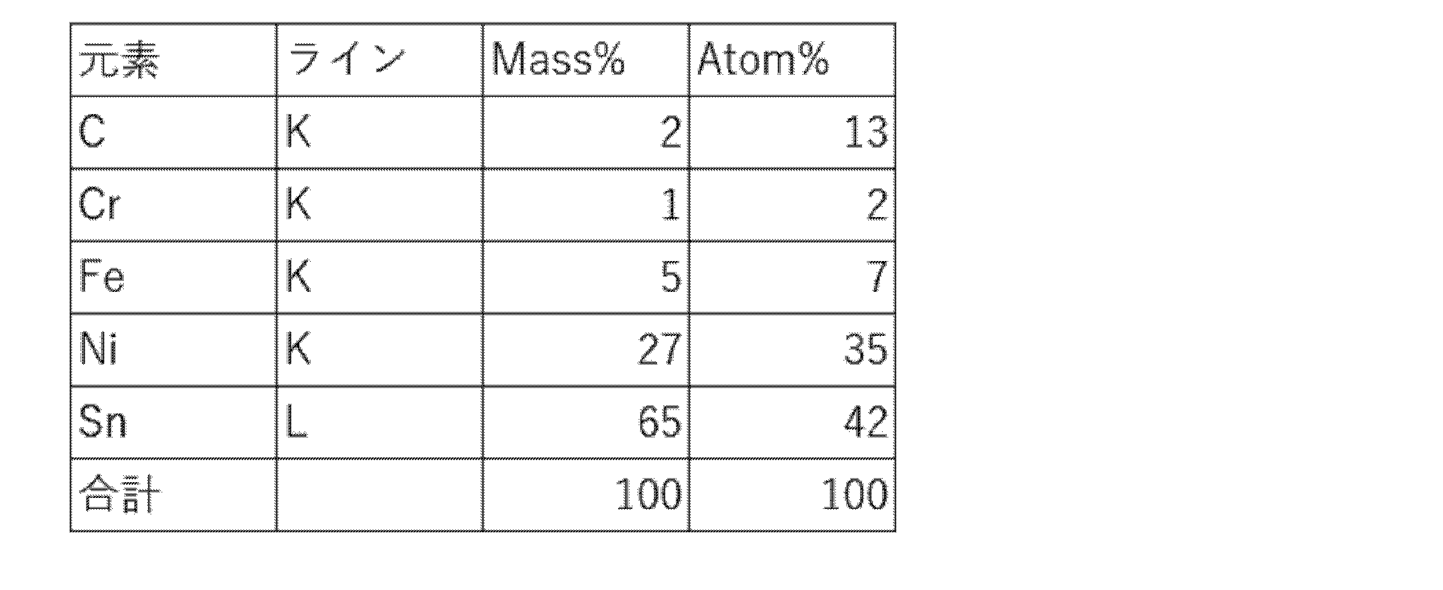
以下、図12D~図12Fに加えて、図12Gも用いて、本開示の第1の凸部100Acおよび第2の凸部100Bcについて説明する。
金属端子の表面の表面粗さパラメータの測定方法は以下のとおりである。まず、外装材を溶剤により溶かして、金属端子の表面を露出させる。外装材がエポキシ樹脂の場合、溶剤としては、例えば炭化水素系剥離剤が用いられる。露出した金属端子の表面の金属間化合物の表面の表面粗さパラメータを、レーザー顕微鏡を用いて測定する。
・レーザー顕微鏡:形状解析レーザー顕微鏡VK-X100(株式会社キーエンス社製)
・ピッチ:0.08μm
・視野範囲:150μm×150μm
・線粗さ測定時の基準長さ:VK-Xでの標準基準長さ
・カットオフ:無し
2 積層セラミックコンデンサ本体(積層セラミック電子部品本体)
3 外装材
5 接合材
5A 接合材
5B 接合材
10 積層体
20 誘電体層(セラミック層)
30 内部電極層(内部導体層)
100A 第1の金属端子
110A1 第1の接合面
100Ab2 第1の最外表面めっき膜(第1の最外表面金属膜)
100Ac 第1の凸部
100B 第2の金属端子
110B1 第2の接合面
100Bb2 第2の最外表面めっき膜(第2の最外表面金属膜)
100Bc 第2の凸部
E1a 第1の金属間化合物の表面(第1の低ぬれ性表面)
E1b 第1の金属間化合物の表面(第1の低ぬれ性表面)
E1c 第1の金属間化合物の表面(第1の低ぬれ性表面)
E2a 第2の金属間化合物の表面(第2の低ぬれ性表面)
E2b 第2の金属間化合物の表面(第2の低ぬれ性表面)
E2c 第2の金属間化合物の表面(第2の低ぬれ性表面)
CS1 第1の接触面
CS2 第2の接触面
L 長さ方向
LS1 第1の端面
LS2 第2の端面
T 高さ方向
TS1 第1の主面
TS2 第2の主面
U 突起部
W 幅方向
WS1 第1の側面
WS2 第2の側面
Claims (19)
- 積層された複数のセラミック層と積層された複数の内部導体層とを含み、高さ方向に相対する第1の主面および第2の主面と、高さ方向に直交する幅方向に相対する第1の側面および第2の側面と、高さ方向および幅方向に直交する長さ方向に相対する第1の端面および第2の端面と、を含む積層体と、前記第1の端面側に配置される第1の外部電極と、前記第2の端面側に配置される第2の外部電極と、を有する積層セラミック電子部品本体と、
接合材を介して前記第1の外部電極に接続される第1の金属端子と、
接合材を介して前記第2の外部電極に接続される第2の金属端子と、
前記積層セラミック電子部品本体と、前記第1の金属端子の一部と、前記第2の金属端子の一部と、を覆う外装材と、
を備える、積層セラミック電子部品であって、
前記第1の金属端子は、前記接合材と接合している第1の接合面と、前記外装材と接触している第1の接触面と、を有し、
前記第2の金属端子は、前記接合材と接合している第2の接合面と、前記外装材と接触している第2の接触面と、を有し、
前記外装材と接触している第1の接触面は、第1の最外表面金属膜の表面と、前記第1の最外表面金属膜よりもぬれ性の低い第1の低ぬれ性表面と、を備え、
前記外装材と接触している第2の接触面は、第2の最外表面金属膜の表面と、前記第2の最外表面金属膜よりもぬれ性の低い第2の低ぬれ性表面と、を備え、
前記第1の最外表面金属膜の表面と前記第1の低ぬれ性表面との境界部に、第1の凸部が配置され、
前記第2の最外表面金属膜の表面と前記第2の低ぬれ性表面との境界部に、第2の凸部が配置されている、積層セラミック電子部品。 - 前記第1の凸部は、アンダカット形状を有し、
前記第2の凸部は、アンダカット形状を有する、請求項1に記載の積層セラミック電子部品。 - 前記第1の金属端子は、第1の母材と、前記第1の母材の表面に形成された第1のめっき膜を含み、
前記第2の金属端子は、第2の母材と、前記第2の母材の表面に形成された第2のめっき膜を含み、
前記第1の最外表面金属膜は、前記第1のめっき膜の少なくとも最外表面部を含み、
前記第2の最外表面金属膜は、前記第2のめっき膜の少なくとも最外表面部を含む、請求項1または請求項2に記載の積層セラミック電子部品。 - 前記第1のめっき膜は、前記第1の最外表面金属膜を構成する第1の最外表面めっき膜と、前記第1の最外表面めっき膜の下層に配置された第1の下層めっき膜と、を含み、
前記第2のめっき膜は、前記第2の最外表面金属膜を構成する第2の最外表面めっき膜と、前記第2の最外表面めっき膜の下層に配置された第2の下層めっき膜と、を含む、請求項3に記載の積層セラミック電子部品。 - 前記第1の凸部の隆起高さは、前記第1の下層めっき膜の厚みよりも大きく、
前記第2の凸部の隆起高さは、前記第2の下層めっき膜の厚みよりも大きい、請求項4に記載の積層セラミック電子部品。 - 前記第1の最外表面めっき膜および前記第2の最外表面めっき膜はSnめっき膜であり、
前記第1の下層めっき膜および前記第2の下層めっき膜はNiめっき膜である、請求項4または請求項5に記載の積層セラミック電子部品。 - 前記第1の低ぬれ性表面は、前記第1の最外表面めっき膜を構成する金属と前記第1の下層めっき膜を構成する金属とにより構成される第1の金属間化合物の表面であり、
前記第2の低ぬれ性表面は、前記第2の最外表面めっき膜を構成する金属と前記第2の下層めっき膜を構成する金属とにより構成される第2の金属間化合物の表面である、請求項4~6のいずれか1項に記載の積層セラミック電子部品。 - 前記第1の金属間化合物および前記第2の金属間化合物は、NiとSnの金属間化合物により構成されている、請求項7に記載の積層セラミック電子部品。
- 前記第1の低ぬれ性表面は、前記第1の金属端子の前記第1の下層めっき膜の表面であり、
前記第2の低ぬれ性表面は、前記第2の金属端子の前記第2の下層めっき膜の表面である、請求項4~6のいずれか1項に記載の積層セラミック電子部品。 - 前記第1の低ぬれ性表面は、前記第1の金属端子の前記第1の母材の表面であり、
前記第2の低ぬれ性表面は、前記第2の金属端子の前記第2の母材の表面である、請求項3~6のいずれか1項に記載の積層セラミック電子部品。 - 前記第1の金属端子および前記第2の金属端子は、前記積層セラミック電子部品が実装されるべき実装基板の実装面に実装される金属端子であり、
前記積層体の前記第1の主面は、前記実装面と対向する面であり、
前記第1の外部電極は、少なくとも前記第1の主面上の前記第1の端面側に配置され、
前記第2の外部電極は、少なくとも前記第1の主面上の前記第2の端面側に配置され、
前記第1の金属端子は、
前記第1の主面と対向し、前記第1の外部電極に接続される第1の接合部と、
前記第1の接合部に接続され、前記実装面から遠ざかるように延びる第1の立ち上がり部と、
前記第1の立ち上がり部に接続され、前記積層セラミック電子部品本体から遠ざかるように延びる第1の延長部と、を含み、
前記第2の金属端子は、
前記第1の主面と対向し、前記第2の外部電極に接続される第2の接合部と、
前記第2の接合部に接続され、前記実装面から遠ざかるように延びる第2の立ち上がり部と、
前記第2の立ち上がり部に接続され、前記積層セラミック電子部品本体から遠ざかるように延びる第2の延長部と、を含む、請求項4~6のいずれか1項に記載の積層セラミック電子部品。
- 前記第1の金属端子は、前記第1の外部電極が接合される前記第1の接合面側の第1の正面と、前記第1の正面とは反対側の面である第1の反対面と、前記第1の正面と前記第1の反対面とを繋ぐ第1の端子側面と、を含む板状部材であり、
前記第2の金属端子は、前記第2の外部電極が接合される前記第2の接合面側の第2の正面と、前記第2の正面とは反対側の面である第2の反対面と、前記第2の正面と前記第2の反対面とを繋ぐ第2の端子側面と、を含む板状部材である、請求項11に記載の積層セラミック電子部品。 - 前記第1の接触面に設けられた前記第1の低ぬれ性表面は、前記第1の正面において、前記第1の立ち上がり部の中央と前記第1の接合部の間の表面の少なくとも一部と、前記第1の延長部と、に離間して設けられ、
前記第2の接触面に設けられた前記第2の低ぬれ性表面は、前記第2の正面において、前記第2の立ち上がり部の中央と前記第2の接合部の間の表面の少なくとも一部と、前記第2の延長部と、に離間して設けられている、請求項12に記載の積層セラミック電子部品。 - 前記第1の接触面に設けられた前記第1の低ぬれ性表面は、前記第1の延長部の前記第1の正面におよび前記第1の反対面に設けられ、
前記第2の接触面に設けられた前記第2の低ぬれ性表面は、前記第2の延長部の前記第2の正面におよび前記第2の反対面に設けられている、請求項12または請求項13に記載の積層セラミック電子部品。 - 前記第1の接合部の前記第1の反対面に、前記第1の接触面に設けられた前記第1の低ぬれ性表面が設けられ、
前記第2の接合部の前記第2の反対面に、前記第2の接触面に設けられた前記第2の低ぬれ性表面が設けられている、請求項12~14のいずれか1項に記載の積層セラミック電子部品。 - 前記第1の接触面は、前記外装材に接触する表面として、前記第1の最外表面金属膜の表面と、前記第1の低ぬれ性表面と、前記第1の母材の表面と、を含み、
前記第2の接触面は、前記外装材に接触する表面として、前記第2の最外表面金属膜の表面と、前記第2の低ぬれ性表面と、前記第2の母材の表面と、を含む、請求項12に記載の積層セラミック電子部品。 - 前記第1の接触面は、前記第1の接合部において、前記第1の正面に位置する前記第1の最外表面金属膜の表面と、前記第1の反対面に位置する前記第1の低ぬれ性表面と、側面に位置する前記第1の母材の表面と、を含み、
前記第2の接触面は、前記第2の接合部において、前記第2の正面に位置する前記第2の最外表面金属膜の表面と、前記第2の反対面に位置する前記第2の低ぬれ性表面と、側面に位置する前記第2の母材の表面と、を含む、請求項16に記載の積層セラミック電子部品。 - 前記第1の接触面は、前記第1の立ち上がり部の中央と前記第1の接合部の間の表面の少なくとも一部において、前記第1の正面に位置する前記第1の低ぬれ性表面と、前記第1の反対面に位置する前記第1の最外表面金属膜の表面と、側面に位置する前記第1の母材の表面と、を含み、
前記第2の接触面は、前記第2の立ち上がり部の中央と前記第2の接合部の間の表面の少なくとも一部において、前記第2の正面に位置する前記第2の低ぬれ性表面と、前記第2の反対面に位置する前記第2の最外表面金属膜の表面と、側面に位置する前記第2の母材の表面と、を含む、請求項16または請求項17に記載の積層セラミック電子部品。 - 前記第1の接触面に設けられた前記第1の低ぬれ性表面は、前記第1の金属端子に形成された穴または切り欠きにより、前記幅方向に分離され、
前記第2の接触面に設けられた前記第2の低ぬれ性表面は、前記第2の金属端子に形成された穴または切り欠きにより、前記幅方向に分離されている、請求項1~18のいずれか1項に記載の積層セラミック電子部品。
Priority Applications (6)
| Application Number | Priority Date | Filing Date | Title |
|---|---|---|---|
| EP23921573.4A EP4746010A1 (en) | 2023-07-13 | 2023-07-13 | MULTI-LAYER CERAMIC ELECTRONIC COMPONENT |
| CN202380099208.0A CN121263862A (zh) | 2023-07-13 | 2023-07-13 | 层叠陶瓷电子部件 |
| PCT/JP2023/025949 WO2025013299A1 (ja) | 2023-07-13 | 2023-07-13 | 積層セラミック電子部品 |
| JP2025532362A JPWO2025013299A1 (ja) | 2023-07-13 | 2023-07-13 | |
| KR1020267000270A KR20260012831A (ko) | 2023-07-13 | 2023-07-13 | 적층 세라믹 전자부품 |
| US18/797,740 US20250022658A1 (en) | 2023-07-13 | 2024-08-08 | Multilayer ceramic electronic component |
Applications Claiming Priority (1)
| Application Number | Priority Date | Filing Date | Title |
|---|---|---|---|
| PCT/JP2023/025949 WO2025013299A1 (ja) | 2023-07-13 | 2023-07-13 | 積層セラミック電子部品 |
Related Child Applications (1)
| Application Number | Title | Priority Date | Filing Date |
|---|---|---|---|
| US18/797,740 Continuation US20250022658A1 (en) | 2023-07-13 | 2024-08-08 | Multilayer ceramic electronic component |
Publications (1)
| Publication Number | Publication Date |
|---|---|
| WO2025013299A1 true WO2025013299A1 (ja) | 2025-01-16 |
Family
ID=94211565
Family Applications (1)
| Application Number | Title | Priority Date | Filing Date |
|---|---|---|---|
| PCT/JP2023/025949 Ceased WO2025013299A1 (ja) | 2023-07-13 | 2023-07-13 | 積層セラミック電子部品 |
Country Status (6)
| Country | Link |
|---|---|
| US (1) | US20250022658A1 (ja) |
| EP (1) | EP4746010A1 (ja) |
| JP (1) | JPWO2025013299A1 (ja) |
| KR (1) | KR20260012831A (ja) |
| CN (1) | CN121263862A (ja) |
| WO (1) | WO2025013299A1 (ja) |
Citations (5)
| Publication number | Priority date | Publication date | Assignee | Title |
|---|---|---|---|---|
| JP2008166457A (ja) * | 2006-12-28 | 2008-07-17 | Showa Denki Kk | 電子部品のリード端子の構造 |
| JP2019145767A (ja) | 2018-02-19 | 2019-08-29 | サムソン エレクトロ−メカニックス カンパニーリミテッド. | 電子部品 |
| JP2020004832A (ja) * | 2018-06-27 | 2020-01-09 | 株式会社村田製作所 | 積層セラミック電子部品 |
| JP2022142240A (ja) * | 2021-03-16 | 2022-09-30 | 株式会社村田製作所 | 積層セラミックコンデンサ |
| JP2023042425A (ja) * | 2021-09-14 | 2023-03-27 | 株式会社村田製作所 | 積層セラミック電子部品 |
Family Cites Families (3)
| Publication number | Priority date | Publication date | Assignee | Title |
|---|---|---|---|---|
| JP5126379B2 (ja) * | 2011-03-25 | 2013-01-23 | 株式会社村田製作所 | チップ部品構造体 |
| JP7019946B2 (ja) * | 2016-12-05 | 2022-02-16 | 株式会社村田製作所 | 積層コンデンサ内蔵基板 |
| JP7097761B2 (ja) * | 2018-06-27 | 2022-07-08 | 株式会社村田製作所 | 積層セラミック電子部品 |
-
2023
- 2023-07-13 JP JP2025532362A patent/JPWO2025013299A1/ja active Pending
- 2023-07-13 CN CN202380099208.0A patent/CN121263862A/zh active Pending
- 2023-07-13 KR KR1020267000270A patent/KR20260012831A/ko active Pending
- 2023-07-13 EP EP23921573.4A patent/EP4746010A1/en active Pending
- 2023-07-13 WO PCT/JP2023/025949 patent/WO2025013299A1/ja not_active Ceased
-
2024
- 2024-08-08 US US18/797,740 patent/US20250022658A1/en active Pending
Patent Citations (5)
| Publication number | Priority date | Publication date | Assignee | Title |
|---|---|---|---|---|
| JP2008166457A (ja) * | 2006-12-28 | 2008-07-17 | Showa Denki Kk | 電子部品のリード端子の構造 |
| JP2019145767A (ja) | 2018-02-19 | 2019-08-29 | サムソン エレクトロ−メカニックス カンパニーリミテッド. | 電子部品 |
| JP2020004832A (ja) * | 2018-06-27 | 2020-01-09 | 株式会社村田製作所 | 積層セラミック電子部品 |
| JP2022142240A (ja) * | 2021-03-16 | 2022-09-30 | 株式会社村田製作所 | 積層セラミックコンデンサ |
| JP2023042425A (ja) * | 2021-09-14 | 2023-03-27 | 株式会社村田製作所 | 積層セラミック電子部品 |
Also Published As
| Publication number | Publication date |
|---|---|
| EP4746010A1 (en) | 2026-05-20 |
| CN121263862A (zh) | 2026-01-02 |
| KR20260012831A (ko) | 2026-01-27 |
| US20250022658A1 (en) | 2025-01-16 |
| JPWO2025013299A1 (ja) | 2025-01-16 |
Similar Documents
| Publication | Publication Date | Title |
|---|---|---|
| US10790092B2 (en) | Multilayer ceramic electronic component | |
| JP7670193B2 (ja) | 積層セラミックコンデンサおよび積層セラミックコンデンサの実装構造 | |
| US11527364B2 (en) | Multilayer ceramic electronic component including a plurality of bodies and metal terminals connected to outer electrodes | |
| US11887787B2 (en) | Multilayer ceramic electronic component including metal terminals with recess portions and mounting structure of the multilayer ceramic electronic component | |
| WO2025004199A1 (ja) | 積層セラミック電子部品 | |
| US12334267B2 (en) | Multilayer ceramic capacitor | |
| JP7494808B2 (ja) | 積層セラミック電子部品 | |
| JP7609028B2 (ja) | 積層セラミック電子部品 | |
| JP7567728B2 (ja) | 積層セラミック電子部品 | |
| US12456581B2 (en) | Multilayer ceramic electronic component | |
| EP4611011A1 (en) | Layered ceramic electronic component | |
| JP7729475B2 (ja) | 積層セラミックコンデンサ | |
| US20250022658A1 (en) | Multilayer ceramic electronic component | |
| EP4600985A1 (en) | Multilayer ceramic electronic component | |
| US12437931B2 (en) | Multilayer ceramic electronic component | |
| JP2023045850A (ja) | 積層セラミックコンデンサ | |
| US20260081079A1 (en) | Multilayer ceramic capacitor | |
| JP2024134980A (ja) | 電子部品構造体 |
Legal Events
| Date | Code | Title | Description |
|---|---|---|---|
| 121 | Ep: the epo has been informed by wipo that ep was designated in this application |
Ref document number: 23921573 Country of ref document: EP Kind code of ref document: A1 |
|
| ENP | Entry into the national phase |
Ref document number: 2025532362 Country of ref document: JP Kind code of ref document: A |
|
| ENP | Entry into the national phase |
Ref document number: 1020267000270 Country of ref document: KR Free format text: ST27 STATUS EVENT CODE: A-0-1-A10-A15-NAP-PA0105 (AS PROVIDED BY THE NATIONAL OFFICE) |
|
| WWE | Wipo information: entry into national phase |
Ref document number: 1020267000270 Country of ref document: KR |
|
| WWP | Wipo information: published in national office |
Ref document number: 1020267000270 Country of ref document: KR |
|
| NENP | Non-entry into the national phase |
Ref country code: DE |