WO2025013201A1 - モードフィルタおよびそれを備えた光回路 - Google Patents
モードフィルタおよびそれを備えた光回路 Download PDFInfo
- Publication number
- WO2025013201A1 WO2025013201A1 PCT/JP2023/025576 JP2023025576W WO2025013201A1 WO 2025013201 A1 WO2025013201 A1 WO 2025013201A1 JP 2023025576 W JP2023025576 W JP 2023025576W WO 2025013201 A1 WO2025013201 A1 WO 2025013201A1
- Authority
- WO
- WIPO (PCT)
- Prior art keywords
- optical
- section
- core
- optical waveguide
- mode filter
- Prior art date
- Legal status (The legal status is an assumption and is not a legal conclusion. Google has not performed a legal analysis and makes no representation as to the accuracy of the status listed.)
- Pending
Links
Images





Classifications
-
- G—PHYSICS
- G02—OPTICS
- G02B—OPTICAL ELEMENTS, SYSTEMS OR APPARATUS
- G02B6/00—Light guides; Structural details of arrangements comprising light guides and other optical elements, e.g. couplings
- G02B6/10—Light guides; Structural details of arrangements comprising light guides and other optical elements, e.g. couplings of the optical waveguide type
- G02B6/12—Light guides; Structural details of arrangements comprising light guides and other optical elements, e.g. couplings of the optical waveguide type of the integrated circuit kind
Definitions
- This disclosure relates to a mode filter and an optical circuit having the same.
- the silica-based planar lightwave circuit (see, for example, Non-Patent Document 1), which has been developed in the field of optical communications, is an embedded optical waveguide in which a core with a high refractive index and a cladding with a low refractive index are fabricated on a substrate such as silicon using glass deposition technology and semiconductor microfabrication technology.
- PLC is a technology that can realize functions such as branching of light, multiplexing and demultiplexing of wavelengths, and switching of optical paths on a single chip depending on the shape of the core.
- RGB couplers that multiplex the three primary colors of visible light RGB (R: red light, G: green light, B: blue light) (see, for example, Patent Document 1) and optical multiplexing circuits used for atomic cooling of optical lattice clocks, and there are increasing opportunities to process light of a wider range of wavelengths on the same chip.
- Optical circuits are usually designed with a core size that satisfies the single-mode condition.
- the core will be very small for the long wavelengths, which will result in weak light confinement, a large minimum bending radius, and a large chip.
- the core is made larger to match the long wavelengths, multi-mode conditions will be met for short wavelengths, and if there is a field mismatch at the input, higher-order modes will be excited in both the vertical and horizontal directions.
- the multimode condition is expressed by the V parameter (also called the normalized frequency).
- V ⁇ dNA/ ⁇ , where ⁇ is the wavelength, d is the core diameter, and NA is the core numerical aperture.
- the multimode condition occurs when V ⁇ 2.
- the core size is sometimes increased to reduce the light energy density and suppress the change in refractive index. In this case, the same problem occurs because the multimode condition is likely to occur.
- FIG. 1 shows the schematic configuration of an RGB coupler.
- the RGB coupler 100 comprises an optical waveguide 104 formed on a substrate 102 for inputting light, an optical multiplexing circuit 112 for multiplexing the input light, and an optical waveguide 114 for outputting the multiplexed light. Between the optical waveguide 104 and the optical multiplexing circuit 112, the RGB coupler 100 also comprises an optical branching circuit 106 for branching the light input to the optical waveguide 104 into main light and monitor light, an optical waveguide 108 for inputting the main light to the optical multiplexing circuit 112, and an optical waveguide 110 for outputting the monitor light.
- the symbols of the elements for inputting, branching, and guiding R, G, and B, respectively, are identified by adding R, G, and B to the end. Furthermore, in Figure 1, the elements that make up each functional section of the RGB coupler 100 are surrounded by dashed lines and shown as an input section 120, a branching section 122, a multiplexing section 124, a main output section 126, and a monitor output section 128.
- the XZ plane is the main surface of the substrate 102 on which the optical circuit is formed, Z is the light propagation direction, and Y is the thickness direction of the substrate 102.
- the optical multiplexing circuit 112 constituting the multiplexing section 124 can be configured to multiplex G and B using a first directional coupler, and then further multiplex the multiplexed G, B and R using a second directional coupler.
- the optical multiplexing circuit 112 may be configured to use a multimode (MM) conversion waveguide as the second directional coupler to further multiplex the R, G and B multiplexed by the first directional coupler (see, for example, FIG. 4 of Patent Document 1).
- the multiplexing section 124 may be configured using a multimode interferometer (MMI) waveguide.
- MMI multimode interferometer
- the RGB coupler 100 In the RGB coupler 100, light input to the input section 120 directly from a light source (not shown) such as a laser diode (LD) or via an optical waveguide (not shown) such as a fiber is branched into main light and monitor light at the branching section 122.
- the monitor light is emitted into space from the monitor output section 128, which is provided in a position where it can be optically connected to a monitor PD (not shown).
- the main light is R, G, and B combined at the combining section 124 and emitted into space from the main output section 126 (i.e., via one optical waveguide 114).
- FIG. 2 shows the schematic configuration of another RGB coupler, which is a modified example of the RGB coupler 100 in FIG. 1.
- the optical waveguide 110 may be bent by 90 degrees, and the main output section 126 and the monitor output section 128 may be disposed on different end faces.
- the core size of the optical waveguide 104 constituting the input section 120 is a multimode condition, higher modes are excited due to field mismatch or misalignment.
- the branching ratio changes depending on the state of the higher mode, causing the characteristics of the optical circuit to become unstable.
- a mode filter with a narrower optical waveguide width was conventionally inserted.
- FIG 3 shows the schematic configuration of an RGB coupler with a mode filter inserted.
- the RGB coupler 300 shown in Figure 3 is obtained by inserting a mode filter section 320 between the input section 120 and the branch section 122 of the RGB coupler 100 in Figure 1.
- the mode filter section 320 is composed of an optical waveguide that is coupled to the optical waveguide 104 and the optical branch circuit 106 and has a narrower width than the optical waveguide 104.
- the mode filter 304 has a tapered shape on the optical waveguide 104 side that narrows along the light propagation direction, and has a shape with a constant narrow width on the optical branch circuit 106 side.
- the mode filter section 320 composed of the mode filter 304 with a narrow width that can be realistically manufactured may not be able to filter higher-order modes.
- Figures 4(a) and (b) show the propagation of LP11a and LP11b in a narrow mode filter 304.
- Figure 4 shows the propagation of LP11a and LP11b at a wavelength of 445 nm when a mode filter 304 with a width of 1 ⁇ m and a length of 100 ⁇ m is formed on a substrate 102 with a 1% refractive index difference between the core layer and the clad layer and a core layer thickness of 2 ⁇ m.
- LP11a which is a high-order mode in the horizontal direction, is cut by 95% by narrowing the width of the optical waveguide.
- This disclosure has been made in consideration of these problems, and its purpose is to provide a mode filter that filters higher-order modes in both vertical and horizontal directions. This disclosure also provides an optical circuit that has this mode filter.
- An optical circuit includes a substrate, a plurality of input waveguides having a V parameter value of 2 or more, and a plurality of the above-mentioned mode filters connected to each of the plurality of input waveguides.
- FIG. 1 is a top view showing a schematic configuration of a conventional RGB coupler.
- FIG. 1 is a top view showing a schematic configuration of a conventional RGB coupler.
- FIG. 1 is a top view showing a schematic configuration of a conventional RGB coupler.
- 1A and 1B are diagrams for explaining the propagation of light in a narrow optical waveguide of a conventional mode filter, in which (a) is a diagram for explaining the propagation of a high-order mode in the horizontal direction, and (b) is a diagram for explaining the propagation of a high-order mode in the vertical direction.
- FIG. 1 is a top view illustrating a schematic configuration of a mode filter according to an embodiment of the present disclosure.
- FIG. 1A and 1B are diagrams for explaining the propagation of light in a narrow optical waveguide of a mode filter of the present disclosure, in which (a) is a diagram for explaining the propagation of a high-order mode in the horizontal direction, and (b) is a diagram for explaining the propagation of a high-order mode in the vertical direction.
- FIG. 1 is a top view illustrating a schematic configuration of a mode filter according to an embodiment of the present disclosure.
- 5 is a diagram showing the relationship between the optical waveguide width and the transmittance of a mode filter according to an embodiment of the present disclosure.
- FIG. FIG. 1 is a top view showing a schematic configuration of an optical circuit according to an embodiment of the present disclosure.
- FIG. 1 is a top view showing a schematic configuration of an optical circuit according to an embodiment of the present disclosure.
- FIG. 1 is a top view showing a schematic configuration of an optical circuit according to an embodiment of the present disclosure.
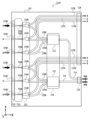
- FIG. 1 is a top view showing a schematic configuration of an optical
- the mode filter 500 shown in Fig. 5 can be inserted between the optical waveguide 104 constituting the input section 120 of the RGB coupler 100 described above with reference to Fig. 1 and the optical branching circuit 106 constituting the branching section 122 to form a mode filter section 520.
- the mode filter 500 can also be inserted into the RGB coupler 200 described above with reference to Fig. 2.
- the width (core width) and thickness (core thickness) of the optical waveguide 104 in the input section 120 are assumed to be in a multimode condition.
- the width of the optical waveguide 104 may be configured to match the field of the LD 510 or fiber (not shown) connected to the optical waveguide 104 of the input section, or may be intentionally made wider to increase the mounting tolerance.
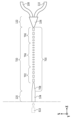
- the mode filter 500 shown in FIG. 5 includes a first section (also called a core length decreasing section) 502 on the optical waveguide 104 side, where the core length (length in the Z direction) decreases (shortens) for each segment in the direction of light propagation, a third section (also called a core length increasing section) 506 on the optical branching circuit 106 side, where the core length increases (lengthens) for each segment in the direction of light propagation, and a second section (also called a core length constant section) between the first and third sections, where the core length for each segment is constant (unchanging).
- the first and third sections gradually increase and decrease the core length so as to suppress loss of optical power in the fundamental mode.
- the mode filter 500 formed on the substrate 102 has a core width of 2.7 ⁇ m and a core thickness of 2 ⁇ m.
- the lengths in the Z direction of the three sections 502, 504, and 506 are 40 ⁇ m, 120 ⁇ m, and 40 m, respectively.
- the pitch between two adjacent cores in each section is 4 ⁇ m. In other words, the length of one segment is 4 ⁇ m.
- the constant core length section 504 is segmented into 30 pieces.
- the length of the core in one segment in the Z direction (also called the optical waveguide length) is 1.3 ⁇ m, and the pitch between adjacent cores is 4 ⁇ m.
- the distance between two adjacent cores (the length in the Z direction of the part where no core exists) is 2.7 ⁇ m.
- the core in the core length decreasing section 502, the core is gradually shortened using 10 segments to the length of the core in the constant core length section 504. If a section without a core suddenly appears, the loss of the propagating fundamental mode light increases. Therefore, the interval between two adjacent cores in the light propagation direction is smaller the closer to the optical waveguide 104, and larger the closer to the constant core length section 504 (according to the propagation distance of the light in the core length decreasing section 502), so that it approaches or is equal to 2.7 ⁇ m, which is the core interval in the constant core length section 504. Note that the greater the number of sections without a core, the greater the loss of the propagating fundamental mode light. Therefore, the number of sections without a core and the interval between two adjacent cores must be determined so as to suppress the power loss of the fundamental mode light while propagating it, and not to propagate the excited higher mode light, as described above.
- d 0 the length of the portion of the segment closest to the optical waveguide 104 where no core exists.
- d n the length of the portion of the nth segment (n is an integer of 10 or less in this example) from the optical waveguide 104 where no core exists.
- d 0 and ⁇ d are values that are determined in advance so that the value of d 10 is close to or equal to 2.7 ⁇ m.
- d 0 is often set to be the minimum gap that can be manufactured.
- the cores are arranged in 10 segments. Contrary to the core length decreasing section 502, in the core length increasing section 506, the interval between two adjacent cores in the light propagation direction becomes larger as it approaches the core length constant section 504, becomes closer to or equal to 2.7 ⁇ m, and becomes smaller as it approaches the optical branching circuit 106 (according to the propagation distance of light in the core length increasing section 506).
- d 0 and ⁇ d are values that are determined in advance so that the value of d 0 is close to or equal to 2.7 ⁇ m.
- the values of d 0 and d 10 in the core length increasing section 506 are set to be the values of d 10 and d 0 in the core length decreasing section 501.
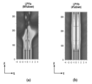
- FIG. 6(a) and (b) show the propagation of LP11a and LP11b in the mode filter 500 in FIG. 5, respectively. From FIG. 6, it can be seen that the transmittance of LP11a and LP11b is 50% and 20%, respectively, and that LP11b, which was not cut by the mode filter 304 using the optical waveguide with a narrower width in the mode filter section 320 shown in FIG. 3, can be effectively cut. In the middle of the optical circuit formed on the substrate 102, the core thickness is constant and there is little distribution in height, so most of the higher-order modes in the vertical direction are generated at the input section 120.
- the mode filter 500 it is important to place the mode filter 500 immediately after the input section 120 to filter the higher-order modes of light, which leads to stabilization of the characteristics of the optical circuit.
- the mode filter 500 since the mode filter 500 more effectively cuts higher-order modes, the transmission characteristics of LP11 are shown in FIG. 6 as higher-order modes.
- FIG. 7 A mode filter according to the second embodiment of the present disclosure will be described with reference to Figures 7 and 8.
- the mode filter 700 shown in Figure 7 is inserted between the optical waveguide 104 constituting the input section 120 of the RGB coupler 100 described above with reference to Figure 1 and the optical branching circuit 106 constituting the branching section 122 to form a mode filter section 720.
- the mode filter 700 can also be inserted into the RGB coupler 200 described above with reference to Figure 2.
- the mode filter section 720 includes a core length decreasing section 702, a constant core length section 704, a core length increasing section 706, and a tapered optical waveguide 708.
- the mode filter section 720 differs from the mode filter section 520 in FIG. 5 in that the core widths (lengths in the X direction) in the core length decreasing section 702, the constant core length section 704, the core length increasing section 706, and the tapered optical waveguide 708 are narrow, and in that the mode filter section 720 includes a mode filter 500 that reduces the core width of the optical waveguide 104 to the core width of the core length decreasing section 702.
- Other aspects of the mode filter section 720 are the same as those of the mode filter 500, so a description thereof will be omitted.
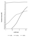
- Figure 8 shows the transmittance of LP01, the fundamental mode, LP11a, the first-order horizontal mode, and LP11b, the first-order vertical mode, at a wavelength of 450 nm, when only the width of the core is changed while the waveguide length (length in the direction of light propagation) of the constant core length section 704 remains the same. From Figure 8, it can be seen that by narrowing the width of the core, it is possible to significantly reduce the transmittance of LP11a and LP11b while keeping the transmittance of LP01 the same.
- the width of the optical waveguide 104 for inputting light is set to a value for obtaining the desired coupling with the fiber or LD. Therefore, it is usually different from the optimal width for filtering higher-order modes.
- a tapered optical waveguide 708 that gradually changes the width of the optical waveguide 104 is arranged to convert it to a width of the optical waveguide that obtains the desired filtering effect.
- the core widths in the core length decreasing section 702, the core length constant section 704, and the core length increasing section 706 are made too thin, a loss in LP01 will also occur.
- by making the core width 1.5 ⁇ m or more low-loss and highly efficient filtering of higher-order modes is possible. In this case, it is desirable to directly connect the tapered optical waveguide 708 and the core length decreasing section 702 to avoid increasing the size of the optical circuit.
- the optical multiplexing circuit 900 shown in FIG. 9 is obtained by inserting the mode filter 500 shown in FIG. 5 between the optical waveguide 104 constituting the input section 120 of the RGB coupler 100 described above with reference to FIG. 1 and the optical branching circuit 106 constituting the branching section 122.
- the mode filter 500 constitutes a mode filter section 520 that does not transmit higher-order modes in both vertical and horizontal directions.
- the optical multiplexing circuit 900 functions as an RGB coupler.
- the light multiplexed by the optical multiplexing circuit 900 is not limited to the three primary colors.
- the optical multiplexing circuit 900 can be an optical circuit configured to multiplex two or more lights in any wavelength region.
- the optical multiplexing circuit 900 shown in FIG. 9 includes an optical waveguide 104 that inputs light, a mode filter 500, an optical multiplexing circuit 112 that multiplexes the input light, and an optical waveguide 114 that outputs the multiplexed light, all formed on a substrate 102. Similar to the RGB coupler 100, the optical multiplexing circuit 900 also includes, between the optical waveguide 104 and the optical multiplexing circuit 112, an optical branching circuit 106 that branches the light input to the optical waveguide 104 into main light and monitor light, an optical waveguide 108 that inputs the main light to the optical multiplexing circuit 112, and an optical waveguide 110 that outputs the monitor light.
- the core thickness of the optical circuit may be set to a multimode condition for all wavelengths of the input light (in this embodiment, R, G, B). For this reason, it is important to insert a mode filter 500 immediately after the optical waveguide 114 that outputs light in the entire color gamut.
- a mode filter 500 immediately after the optical waveguide 114 that outputs light in the entire color gamut.
- the light output from the main output unit 126 and the monitor output unit 128 contains higher-order modes, this will lead to deterioration of beam quality, such as a shift in the output angle of the light, so it is important that only the fundamental mode propagates to the main output unit 126 and the monitor output unit 128.
- the mode filter 500 described with reference to FIG. 5 is inserted between the optical waveguide 104 that constitutes the input section 120 of the optical multiplexing circuit 900 and the optical branching circuit 106 that constitutes the branching section 122, so that higher-order modes in both the vertical and horizontal directions can be prevented from propagating beyond the optical multiplexing circuit 112. This makes it possible to stabilize the characteristics of the optical circuit.
- the optical waveguide 110 may be bent by 90 degrees and the main output section 126 and the monitor output section 128 may be arranged on different end faces.
- the mode filter 500 shown in FIG. 5 is inserted between the optical waveguide 104 constituting the input section 120 of the RGB coupler 200 described above with reference to FIG. 2 and the optical branching circuit 106 constituting the branching section 122.
- the optical multiplexing circuit 1000 shown in Fig. 10 is obtained by inserting the mode filter 700 shown in Fig. 7 between the optical waveguide 104 constituting the input section 120 of the RGB coupler 100 described above with reference to Fig. 1 and the optical branching circuit 106 constituting the branching section 122.
- the optical multiplexing circuit 1000 functions as an RGB coupler.
- the light multiplexed by the optical multiplexing circuit 1000 is not limited to the three primary colors.
- the optical multiplexing circuit 1000 can be an optical circuit configured to multiplex two or more lights in any wavelength region.
- the optical multiplexing circuit 1000 can more effectively prevent higher-order modes in both the vertical and horizontal directions from propagating beyond the optical multiplexing circuit 112 than the optical multiplexing circuit 900 shown in FIG. 9, thereby enabling further stabilization of the characteristics of the optical circuit.
- the optical waveguide 110 may be bent by 90 degrees and the main output section 126 and the monitor output section 128 may be arranged on different end faces.
- the mode filter 700 shown in FIG. 7 is inserted between the optical waveguide 104 constituting the input section 120 of the RGB coupler 200 described above with reference to FIG. 2 and the optical branching circuit 106 constituting the branching section 122.
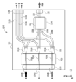
- the optical multiplexing circuit 1100 shown in Fig. 11 has a configuration in which a plurality of optical multiplexing circuits 1000 are arranged on a substrate 102.
- the optical multiplexing circuit 1100 can be used as a multi-beam light source.
- the optical multiplexing circuit 1100 also has a mode filter 700 inserted therein, so that higher-order modes in both vertical and horizontal directions are prevented from propagating beyond the optical multiplexing circuit 112, thereby enabling further stabilization of the characteristics of the optical circuit.
Landscapes
- Physics & Mathematics (AREA)
- Engineering & Computer Science (AREA)
- Microelectronics & Electronic Packaging (AREA)
- General Physics & Mathematics (AREA)
- Optics & Photonics (AREA)
- Optical Integrated Circuits (AREA)
Abstract
本開示の一実施形態は、モードフィルタを提供する。モードフィルタは、光導波路を備える。光導波路は、複数のセグメントにセグメント化されている。複数のセグメントの各々が、コアがある領域およびコアがない領域を有する。光導波路は、第1の区間と、第2の区間と、第3の区間とを含む。第1の区間において、コアがない領域の光の伝搬方向の長さが増大する。第2の区間において、コアがない領域の光の伝搬方向の長さが一定である。第3の区間において、コアがない領域の光の伝搬方向の長さが減少する。本開示の一実施形態は、光回路を提供する。光回路は、基板と、Vパラメータの値が2以上である複数の入力導波路と、複数の入力導波路の各々と接続された前述した複数のモードフィルタとを備える。光回路は、複数のモードフィルタの各々に接続された複数の光分岐回路と、複数の光分岐回路と接続された光合波回路とをさらに備える。
Description
本開示は、モードフィルタおよびそれを有する光回路に関する。
光通信分野で発展してきた石英系平面光波回路(Planar lightwave circuit:PLC)(たとえば非特許文献1参照)は、埋め込み型の光導波路で、屈折率の高いコアと屈折率の低いクラッドがSiなどの基板上にガラスの成膜技術と半導体微細加工技術を用いて作製される。PLCは、コアの形状によって、光の分岐、波長の合分波、光路のスイッチングなどの機能をワンチップで実現できる技術である。近年では、光通信で用いる赤外光だけでなく、可視光のRGB(R:赤色光、G:緑色光、B:青色光)の3原色を合波するRGBカプラ(たとえば特許文献1参照)や光格子時計の原子冷却に用いる光の合波回路など、可視域の波長も取り扱うようになり、より広い範囲の波長の光を同じチップ内で処理する機会が増えている。
通常、光回路は、シングルモード条件を満たすコアサイズで設計される。しかしながら、取り扱う波長域が広くなると、すべての波長域でシングルモード条件を満たすように設計すると、長波長側にとっては、非常に小さいコアとなり、光の閉じ込めが弱く、最小曲げ半径が大きくなり、チップが大型化してしまう。一方で、長波長側に合わせて、コアを大きくすると、短波長ではマルチモード条件となり、入力部でフィールドのミスマッチがあると、縦、横両方向で高次モードが励振されてしまう。
マルチモード条件は、Vパラメータ(規格化周波数とも呼ばれる。)で表現される。V=πdNA/λであり、λは波長、dはコアの径、NAはコアの開口数である。V≧2のときマルチモード条件となる。光回路内において高次モードが励振されると、従来の測定方法では正確に光学特性が評価できなくなることや、光学特性が不安定になってしまう。たとえばRGBカプラでは、長波長側のRの最小曲げ半径が大きくなることや、短波長側のBがマルチモード化するといった問題が生じる。
また、PLCは、短波長の強い光で屈折率が変化するため(たとえば非特許文献2参照)、光のエネルギー密度を下げて屈折率変化を抑制するためにコアサイズを大きくすることがある。この際も、マルチモード条件となりやすいため、同様の問題が生じる。
図1に、RGBカプラの概略構成を示す。RGBカプラ100は、基板102に形成された、光を入力する光導波路104と、入力された光を合波する光合波回路112と、合波した光を出力する光導波路114とを備える。また、RGBカプラ100は、光導波路104と光合波回路112との間に、光導波路104へ入力された光をメイン光とモニタ光とに分岐する光分岐回路106と、メイン光を光合波回路112入力する光導波路108と、モニタ光を出力する光導波路110とを備える。図1において、R,G,Bがそれぞれ入力され、分岐され、導波する要素の符号は、末尾にR,G,Bを付して、それぞれを識別している。さらに、図1には、RGBカプラ100の各機能部を構成する要素を破線で囲み、入力部120と、分岐部122と、合波部124と、メイン出力部126と、モニタ出力部128として示している。XZ面は、光回路が形成される基板102の主面であり、Zは光の伝搬方向であり、Yは基板102の厚さ方向である。
合波部124を構成する光合波回路112は、GとBとを第1の方向性結合器で合波して、次いで、第2の方向性結合器で合波されたGおよびBとRとをさらに合波する構成とすることができる。光合波回路112は、第1の方向性結合器で合波されたRおよびGとBとをさらに合波するために、第2の方向性結合器をマルチモード(MM)変換導波路を使用する構成としてもよい(たとえば特許文献1の図4参照)。あるいは、合波部124を多モード干渉計(Multimode Interferometer:MMI)導波路を用いて構成してもよい。
RGBカプラ100において、レーザーダイオード(Laser Diode;LD)等の光源(不図示)から直接にまたはファイバー等の光導波路(不図示)を介して、入力部120へ入力された光は、分岐部122でメイン光とモニタ光に分岐される。モニタ光は、モニタPD(不図示)と光学的に接続できる位置に設けられたモニタ出力部128から空間に放出される。メイン光は、合波部124でR,G,Bを合波してメイン出力部126から(すなわち1つの光導波路114を介して)空間に放射される。
図2に、図1のRGBカプラ100の変形例である、別のRGBカプラの概略構成を示す。図2に示すRGBカプラ200のように、メイン出力部126とモニタ出力部128と間のクロストークを避けるために、光導波路110を90度曲げて、メイン出力部126とモニタ出力部128とを異なる端面に配置する場合もある。
RGBカプラ100または200において、入力部120を構成する光導波路104のコアのサイズがマルチモード条件の場合、フィールドのミスマッチや位置ずれが原因で高次モードが励振される。高次モードの光が、分岐部122を構成する光分岐回路106または合波部124を構成する方向性結合器に入ると、高次モードの状態によって分岐率が変化するため、光回路の特性が不安定となる。こうした状況をさけるために従来は、光導波路の幅を細くしたモードフィルタを挿入していた。
図3に、モードフィルタを挿入したRGBカプラの概略構成を示す。図3に示すRGBカプラ300は、図1のRGBカプラ100の入力部120と分岐部122との間に、モードフィルタ部320を挿入したものである。モードフィルタ部320は、光導波路104と光分岐回路106とに結合された、光導波路104よりも幅を細くした光導波路で構成されている。図3に示すようにモードフィルタ304は、光導波路104側に、光の伝搬方向に沿って幅が細くなるテーパー形状を有しており、光分岐回路106側に一定の細い幅が続く形状を有する。しかしながら、RGBカプラのように、広い波長域を取り扱う場合、現実的に作製可能な細い幅を有するモードフィルタ304で構成したモードフィルタ部320では高次モードをフィルタリングできないこともある。
A. Himeno, et al., "Silica-Based Planar Lightwave Circuits", Published in: IEEE Journal of Selected Topics in Quantum Electronics, Volume: 4, Issue: 6, 1998, pp.913-924
Y. Fujiwara, et al., "Silica-based planar lightwave circuits with high resistance against blue light for visible-light application", Japanese Journal of Applied Physics, 61, SK1021, 2022
図4(a)および(b)に、細い幅を有するモードフィルタ304におけるLP11aおよびLP11bの伝搬の様子をそれぞれ示す。図4は、例示としてコア層とクラッド層の屈折率差が1%、コア層の厚さが2μmの基板102に、幅が1μm、長さが100μmのモードフィルタ304を形成した場合の波長445nmにおけるLP11aおよびLP11bの伝搬の様子をそれぞれ示す。図4(a)に示すように、横方向の高次モードであるLP11aは、光導波路の幅を細くしたことで95%カットされることがわかる。一方、図4(b)に示すように、縦方向の高次モードであるLP11bは、フィルタリングされることなくほぼそのまま透過することがわかる。幅を細くした光導波路を十分長くして、LP11bを取り除く方法もあるが、チップサイズが大型化するといった問題が生じる。
本開示は、このような問題に鑑みてなされたもので、その目的とするところは、縦および横の双方向の高次モードをフィルタするモードフィルタを提供することにある。また、本開示は、当該モードフィルタを有する光回路を提供することになる。
本開示の一実施形態のモードフィルタは、光導波路を備え、光導波路は、複数のセグメントにセグメント化されており、複数のセグメントの各々が、コアがある領域およびコアがない領域を有し、光導波路は、第1の区間と、第2の区間と、第3の区間とを含み、第1の区間において、コアがない領域の光の伝搬方向の長さが増大し、第2の区間において、コアがない領域の光の伝搬方向の長さが一定であり、第3の区間において、コアがない領域の光の伝搬方向の長さが減少する。
本開示の一実施形態の光回路は、基板と、Vパラメータの値が2以上である複数の入力導波路と、複数の入力導波路の各々と接続された複数の上記モードフィルタとを備える。
本開示によれば、縦および横の双方向の高次モードをフィルタするモードフィルタを提供することができる。また、本開示によれば、モードフィルタを入力部と分岐部との間に配置することで、特性不安定化を抑制した光回路を提供することができる。
する。
する。
以下、図面を参照しながら本開示の種々の実施形態について詳細に説明する。同一または類似の参照符号は、同一または類似の要素を示し、繰り返しの説明を省略する場合がある。以下の説明における数値は例示であり、本科開示の実施形態は要旨を逸脱しない限り他の数値で実施することができる。以下、図5から8を参照して本開示の一実施形態にかかるモードフィルタを説明する。その後、図9から11を参照して本開示の一実施形態にかかる光回路を説明する。
(実施形態1)
図5および図6を参照して、本開示の実施形態1にかかるモードフィルタを説明する。図5に示すモードフィルタ500は、図1を参照して上述したRGBカプラ100の入力部120を構成する光導波路104と、分岐部122を構成する光分岐回路106との間に挿入して、モードフィルタ部520を構成することができる。勿論、モードフィルタ500は、図2を参照して上述したRGBカプラ200に挿入することもできる。入力部120における光導波路104の幅(コアの幅)や厚さ(コアの厚さ)は、マルチモード条件となっているとする。光導波路104の幅は、入力部の光導波路104に接続するLD510またはファイバー(不図示)のフィールドに合わせて構成される場合があり、また実装トレランスを高くするために意図的にと広くする場合などがある。
図5および図6を参照して、本開示の実施形態1にかかるモードフィルタを説明する。図5に示すモードフィルタ500は、図1を参照して上述したRGBカプラ100の入力部120を構成する光導波路104と、分岐部122を構成する光分岐回路106との間に挿入して、モードフィルタ部520を構成することができる。勿論、モードフィルタ500は、図2を参照して上述したRGBカプラ200に挿入することもできる。入力部120における光導波路104の幅(コアの幅)や厚さ(コアの厚さ)は、マルチモード条件となっているとする。光導波路104の幅は、入力部の光導波路104に接続するLD510またはファイバー(不図示)のフィールドに合わせて構成される場合があり、また実装トレランスを高くするために意図的にと広くする場合などがある。
図5に示すモードフィルタ500は、光導波路104側に、セグメント毎にコアの長さ(Z方向の長さ)が光の伝搬方向に向かって減少する(短くなる)第1の区間(コア長減少区間ともいう)502、光分岐回路106側に、セグメント毎にコアの長さが光の伝搬方向に向かって増加する(長くなる)第3の区間(コア長増加区間ともいう)506、および、第1の区間と第3の区間との間に、セグメント毎のコアの長さが一定の(変化しない)第2の区間(コア長一定区間ともいう)を含む。ここで、第1と第3の区間は、基底モードの光パワーの損失を抑えるように徐々にコアの長さを増減させる。
本実施形態において、基板102に形成されたモードフィルタ500は、コアの幅が2.7μm、コアの厚さが2μmである。3つの区間502、504、および506のZ方向の長さはそれぞれ、40μm、120μm、および40mである。各区間において隣接する2つのコアのピッチは4μmである。すなわち一つのセグメントの長さは4μmである。
この例では、コア長一定区間504において、30個にセグメント化されている。1つのセグメントにおけるコアのZ方向の長さ(光導波路長ともいう)は、1.3μmであり、隣接するコアのピッチは4μmである。隣接する2つのコアの間隔(コアが存在しない部分のZ方向の長さ)は2.7μmである。
また、この例では、コア長減少加区間502において、コアは、10個のセグメントを用いて、コア長一定区間504のコアの長さになるように徐々にコアの長さを短くしている。コアが存在しない部分が突然現れると、伝搬する基底モードの光の損失が大きくなる。したがって、光の伝搬方向に向かって隣接する2つのコアの間隔は、光導波路104に近いほど小さく、コア長一定区間504に近いほど(コア長減少加区間502における光の伝搬距離に応じて)大きくなり、コア長一定区間504におけるコアの間隔である2.7μmに近づくか等しくなるようにしている。なお、コアが存在しない部分の数が多いほど、伝搬する基底モードの光の損失が増加する。したがって、コアが存在しない部分の数および隣接する2つのコアの間隔は、上述したように、基底モードの光のパワーの損失を抑制しつつ伝搬させるように、且つ励振した高次モードの光を伝搬させないように、決定する必要がある。
図5に示すように、光導波路104に最も近いセグメントにおけるコアが存在しない部分の長さをd0とすると、光導波路104側からn番目(この例では、nは10以下の整数)のセグメントにおけるコアが存在しない部分の長さdnは、dn=d0+Δd(n-1)と表すことができる。d0とΔdは、d10の値が2.7μmに近い値となるか等しくなるよう、予め決定された値である。また、d0は製造可能な最小ギャップとなるように設定することが多い。
一方、この例では、コア長増加区間506においては、コアは、10個のセグメントに配置されている。コア長減少加区間502と反対に、コア長増加区間506において、光の伝搬方向に向かって隣接する2つのコアの間隔は、コア長一定区間504に近いほど大きくなり、2.7μmに近づくか等しくなり、光分岐回路106に近いほど(コア長増加区間506における光の伝搬距離に応じて)小さくなるようにしている。コア長一定区間504側からn番目(この例では、nは10以下の整数)のセグメントにおけるコアが存在しない部分の長さdnは、dn=d0-Δd(n-1)と表すことができる。d0とΔdは、d0の値が2.7μmに近い値となるか等しくなるよう、予め決定された値である。なお、この例では、コア長増加区間506におけるd0とd10の値がコア長減少区間501のd10とd0の値となるように設定している。
図6(a)および(b)に、図5のモードフィルタ500におけるLP11aおよびLP11bの伝搬の様子をそれぞれ示す。図6から、LP11a、LP11bの透過率が、それぞれ50%、20%となり、図3に示したモードフィルタ部320における幅を細くした光導波路によるモードフィルタ304ではカットされなかったLP11bが効果的にカットできることが分かる。基板102に形成される光回路の途中では、コアの厚さは一定で、高さの分布が少ないため、縦方向の高次モードの殆どが入力部120で発生する。このため、入力部120の直後にモードフィルタ500を配置して光の高次モードをフィルタリングすることは重要であり、光回路の特性の安定化につながる。また、光回路の大型化を避けるために、モードフィルタと分岐部122は直接接続することが望ましい。なお、モードフィルタ500により次数の高い高次モードはより効果的にカットされるため、したがって、図6においては、高次モードとして、LP11の透過特性を示している。
(実施形態2)
図7および図8を参照して、本開示の実施形態2にかかるモードフィルタを説明する。図7に示すモードフィルタ700は、図1を参照して上述したRGBカプラ100の入力部120を構成する光導波路104と、分岐部122を構成する光分岐回路106との間に挿入されて、モードフィルタ部720を構成する。勿論、モードフィルタ700は、図2を参照して上述したRGBカプラ200に挿入することもできる。
図7および図8を参照して、本開示の実施形態2にかかるモードフィルタを説明する。図7に示すモードフィルタ700は、図1を参照して上述したRGBカプラ100の入力部120を構成する光導波路104と、分岐部122を構成する光分岐回路106との間に挿入されて、モードフィルタ部720を構成する。勿論、モードフィルタ700は、図2を参照して上述したRGBカプラ200に挿入することもできる。
モードフィルタ部720は、コア長減少区間702、コア長一定区間704、コア長増加区間706、およびテーパー光導波路708を含む。モードフィルタ部720は、コア長減少区間702、コア長一定区間704、コア長増加区間706、およびテーパー光導波路708におけるコアの幅(X方向の長さ)が狭い点、並びに、光導波路104のコアの幅をコア長減少区間702のコア幅に減少するモードフィルタ500を含む点で、図5のモードフィルタ部520と異なる。モードフィルタ部720のその他の点は、モードフィルタ500と同じであるので説明を省略する。
図8に、コア長一定区間704の導波路長(光の伝搬方向の長さ)をそのままに、コアの幅のみを変えた場合の、波長450nmにおける基底モードであるLP01、横方向の1次モードであるLP11a、縦方向の1次モードであるLP11bそれぞれの透過率を示す。図8から、コアの幅を細くすることで、LP01の透過率はそのままに、LP11aおよびLP11bの透過率を大きく落とすことが可能であることがわかる。光を入力するための光導波路104の幅は、ファイバーやLDと所望の結合を得るための値に設定される。したがって、通常、高次モードをフィルタリングするのに最適な幅とは異なる。このため、本実施形態においては、光導波路104の幅を徐々に変化させるテーパー光導波路708を配置して、所望のフィルタリング効果が得られる光導波路の幅に変換する。ただし、図8から理解されるように、コア長減少区間702、コア長一定区間704、コア長増加区間706におけるコアの幅を細くしすぎると、LP01の損失も発生する。図8から理解されるように、コアの幅を1.5μm以上にすることで、低損失かつ高効率な高次モードのフィルタリングが可能である。この際、光回路の大型化をさけるために、テーパー光導波路708とコア長減少区間702とを直接接続することが望ましい。
(実施形態3)
図9を参照して、本開示の実施形態3にかかる光合波回路を説明する。図9に示す光合波回路900は、図1を参照して上述したRGBカプラ100の入力部120を構成する光導波路104と、分岐部122を構成する光分岐回路106との間に、図5に示したモードフィルタ500を挿入したものである。モードフィルタ500は、縦および横の双方向の高次モードを透過させないようにするモードフィルタ部520を構成する。光合波回路900は、RGBカプラとして機能する。勿論、光合波回路900が合波する光は3原色に限定されない。光合波回路900は、任意の波長領域の2つ以上の光を合波するように構成された光回路とすることができる。
図9を参照して、本開示の実施形態3にかかる光合波回路を説明する。図9に示す光合波回路900は、図1を参照して上述したRGBカプラ100の入力部120を構成する光導波路104と、分岐部122を構成する光分岐回路106との間に、図5に示したモードフィルタ500を挿入したものである。モードフィルタ500は、縦および横の双方向の高次モードを透過させないようにするモードフィルタ部520を構成する。光合波回路900は、RGBカプラとして機能する。勿論、光合波回路900が合波する光は3原色に限定されない。光合波回路900は、任意の波長領域の2つ以上の光を合波するように構成された光回路とすることができる。
図9に示す光合波回路900は、基板102に形成された、光を入力する光導波路104と、モードフィルタ500と、入力された光を合波する光合波回路112と、合波した光を出力する光導波路114とを備える。また、光合波回路900は、RGBカプラ100と同様に、光導波路104と光合波回路112との間に、光導波路104へ入力された光をメイン光とモニタ光とに分岐する光分岐回路106と、メイン光を光合波回路112入力する光導波路108と、モニタ光を出力する光導波路110とを備える。
光合波回路900において所望の出射角やLDとの結合を得るために、入力される光の全ての波長(本実施形態では、R,G,B)において光回路のコアの厚さの設定がマルチモード条件となる場合がある。このため、全色域において光を出力する光導波路114の直後にモードフィルタ500を挿入することが重要である。また、RGBカプラとして、メイン出力部126およびモニタ出力部128から出力される光に高次モードが含まれる場合、光の出射角がずれるなど、ビーム品質の劣化につながるため、メイン出力部126およびモニタ出力部128に伝搬する基底モードのみであることが重要である。
本実施形態では、光合波回路900の入力部120を構成する光導波路104と、分岐部122を構成する光分岐回路106との間に、図5を参照して説明したモードフィルタ500を挿入したことにより、縦および横の双方向の高次モードが光合波回路112以降を伝搬しないようにすることがでる。これにより、光回路の特性の安定化が可能になる。
なお、本実施形態の光合波回路900において、メイン出力部126とモニタ出力部128と間のクロストークを避けるために、光導波路110を90度曲げて、メイン出力部126とモニタ出力部128とを異なる端面に配置してもよい。この場合、図2を参照して上述したRGBカプラ200の入力部120を構成する光導波路104と、分岐部122を構成する光分岐回路106との間に、図5に示したモードフィルタ500を挿入した態様となる。
(実施形態4)
図10を参照して、本開示の実施形態4にかかる光合波回路を説明する。図10に示す光合波回路1000は、図1を参照して上述したRGBカプラ100の入力部120を構成する光導波路104と、分岐部122を構成する光分岐回路106との間に、図7に示したモードフィルタ700を挿入したものである。光合波回路1000は、RGBカプラとして機能する。勿論、光合波回路1000が合波する光は3原色に限定されない。光合波回路1000は、任意の波長領域の2つ以上の光を合波するように構成された光回路とすることができる。
図10を参照して、本開示の実施形態4にかかる光合波回路を説明する。図10に示す光合波回路1000は、図1を参照して上述したRGBカプラ100の入力部120を構成する光導波路104と、分岐部122を構成する光分岐回路106との間に、図7に示したモードフィルタ700を挿入したものである。光合波回路1000は、RGBカプラとして機能する。勿論、光合波回路1000が合波する光は3原色に限定されない。光合波回路1000は、任意の波長領域の2つ以上の光を合波するように構成された光回路とすることができる。
光合波回路1000は、モードフィルタ700を挿入したことにより、図9に示した光合波回路900よりも効果的に、縦および横の双方向の高次モードが光合波回路112以降を伝搬しないようにすることができ、光回路の特性のさらなる安定化が可能になる。
なお、本実施形態の光合波回路1000においても、メイン出力部126とモニタ出力部128と間のクロストークを避けるために、光導波路110を90度曲げて、メイン出力部126とモニタ出力部128とを異なる端面に配置してもよい。この場合、図2を参照して上述したRGBカプラ200の入力部120を構成する光導波路104と、分岐部122を構成する光分岐回路106との間に、図7に示したモードフィルタ700を挿入した態様となる。
(実施形態5)
図11を参照して、本開示の実施形態5にかかる光合波回路を説明する。図11に示す光合波回路1100は、基板102に複数の光合波回路1000を配置した構成である。光合波回路1100は、マルチビーム光源として使用することができる。光合波回路1100もまた、モードフィルタ700を挿入したことにより、縦および横の双方向の高次モードが光合波回路112以降を伝搬しないようにすることができ、光回路の特性のさらなる安定化が可能になる。
図11を参照して、本開示の実施形態5にかかる光合波回路を説明する。図11に示す光合波回路1100は、基板102に複数の光合波回路1000を配置した構成である。光合波回路1100は、マルチビーム光源として使用することができる。光合波回路1100もまた、モードフィルタ700を挿入したことにより、縦および横の双方向の高次モードが光合波回路112以降を伝搬しないようにすることができ、光回路の特性のさらなる安定化が可能になる。
縦および横の双方向の高次モードをフィルタするモードフィルタを提供することが可能となる。また、特性不安定化を抑制した光回路を提供することが可能となる。
100,200,300 RGBカプラ
102 基板
104,104R,104G,104B 光導波路
106,106R,106G,106B 光分岐回路
108,108R,108G,108B 光導波路
110,110R,110G,110B 光導波路
112 光合波回路
114 光導波路
120 入力部
122 分岐部
124 合波部
126 メイン出力部
128 モニタ出力部
304,304R,304G,304B,500、500R,500G,500B,700、700R,700G,700B モードフィルタ
320,520、720 モードフィルタ部
502,702 コア長減少区間
504,704 コア長一定区間
506,706 コア長増加区間
510 レーザーダイオード
708 テーパー光導波路
900,1000,1100 光回路
102 基板
104,104R,104G,104B 光導波路
106,106R,106G,106B 光分岐回路
108,108R,108G,108B 光導波路
110,110R,110G,110B 光導波路
112 光合波回路
114 光導波路
120 入力部
122 分岐部
124 合波部
126 メイン出力部
128 モニタ出力部
304,304R,304G,304B,500、500R,500G,500B,700、700R,700G,700B モードフィルタ
320,520、720 モードフィルタ部
502,702 コア長減少区間
504,704 コア長一定区間
506,706 コア長増加区間
510 レーザーダイオード
708 テーパー光導波路
900,1000,1100 光回路
Claims (5)
- モードフィルタであって、
光導波路を備え、
前記光導波路は、複数のセグメントにセグメント化されており、前記複数のセグメントの各々が、コアがある領域およびコアがない領域を有し、前記光導波路は、第1の区間と、第2の区間と、第3の区間とを含み、
前記第1の区間において、前記コアがない領域の光の伝搬方向の長さが増大し、
前記第2の区間において、前記コアがない領域の光の伝搬方向の長さが一定であり、
前記第3の区間において、前記コアがない領域の光の伝搬方向の長さが減少する、モードフィルタ。 - 前記光導波路の幅は、入力光導波路の幅よりも狭く、
前記入力光導波路の幅を前記光導波路の幅に変換するテーパー光導波路
をさらに備えた、請求項1に記載のモードフィルタ。 - 光回路であって、
基板と、
Vパラメータの値が2以上である複数の入力光導波路と、
前記複数の入力光導波路の各々と接続された請求項1に記載の複数のモードフィルタと
を備えた、光回路。 - 前記複数のモードフィルタの各々に接続された複数の光分岐回路と、
前記複数の光分岐回路と接続された光合波回路と
をさらに備えた、請求項3に記載の光回路。 - 請求項3に記載の光回路を複数備えた光回路。
Priority Applications (2)
| Application Number | Priority Date | Filing Date | Title |
|---|---|---|---|
| PCT/JP2023/025576 WO2025013201A1 (ja) | 2023-07-11 | 2023-07-11 | モードフィルタおよびそれを備えた光回路 |
| JP2025532288A JPWO2025013201A1 (ja) | 2023-07-11 | 2023-07-11 |
Applications Claiming Priority (1)
| Application Number | Priority Date | Filing Date | Title |
|---|---|---|---|
| PCT/JP2023/025576 WO2025013201A1 (ja) | 2023-07-11 | 2023-07-11 | モードフィルタおよびそれを備えた光回路 |
Publications (1)
| Publication Number | Publication Date |
|---|---|
| WO2025013201A1 true WO2025013201A1 (ja) | 2025-01-16 |
Family
ID=94215281
Family Applications (1)
| Application Number | Title | Priority Date | Filing Date |
|---|---|---|---|
| PCT/JP2023/025576 Pending WO2025013201A1 (ja) | 2023-07-11 | 2023-07-11 | モードフィルタおよびそれを備えた光回路 |
Country Status (2)
| Country | Link |
|---|---|
| JP (1) | JPWO2025013201A1 (ja) |
| WO (1) | WO2025013201A1 (ja) |
Citations (8)
| Publication number | Priority date | Publication date | Assignee | Title |
|---|---|---|---|---|
| JPH04172308A (ja) * | 1990-11-05 | 1992-06-19 | Nippon Sheet Glass Co Ltd | Y分岐光回路 |
| JPH08262244A (ja) * | 1995-03-10 | 1996-10-11 | At & T Corp | 集積光学導波管用サイド・ギャップ・モード・テーパリング |
| JP2002006160A (ja) * | 2000-06-23 | 2002-01-09 | Fujitsu Ltd | 光導波路 |
| US20020031304A1 (en) * | 2000-09-13 | 2002-03-14 | Roberts Stephen William | Rib waveguide device with mode filter |
| JP2007279455A (ja) * | 2006-04-07 | 2007-10-25 | Oki Electric Ind Co Ltd | 光反射器及び光学装置 |
| JP2016156928A (ja) * | 2015-02-24 | 2016-09-01 | 沖電気工業株式会社 | スポットサイズ変換器 |
| WO2017159044A1 (ja) * | 2016-03-14 | 2017-09-21 | 日本電気株式会社 | 光分岐回路 |
| WO2021234787A1 (ja) * | 2020-05-18 | 2021-11-25 | 日本電信電話株式会社 | 光合波回路および光源 |
-
2023
- 2023-07-11 JP JP2025532288A patent/JPWO2025013201A1/ja active Pending
- 2023-07-11 WO PCT/JP2023/025576 patent/WO2025013201A1/ja active Pending
Patent Citations (8)
| Publication number | Priority date | Publication date | Assignee | Title |
|---|---|---|---|---|
| JPH04172308A (ja) * | 1990-11-05 | 1992-06-19 | Nippon Sheet Glass Co Ltd | Y分岐光回路 |
| JPH08262244A (ja) * | 1995-03-10 | 1996-10-11 | At & T Corp | 集積光学導波管用サイド・ギャップ・モード・テーパリング |
| JP2002006160A (ja) * | 2000-06-23 | 2002-01-09 | Fujitsu Ltd | 光導波路 |
| US20020031304A1 (en) * | 2000-09-13 | 2002-03-14 | Roberts Stephen William | Rib waveguide device with mode filter |
| JP2007279455A (ja) * | 2006-04-07 | 2007-10-25 | Oki Electric Ind Co Ltd | 光反射器及び光学装置 |
| JP2016156928A (ja) * | 2015-02-24 | 2016-09-01 | 沖電気工業株式会社 | スポットサイズ変換器 |
| WO2017159044A1 (ja) * | 2016-03-14 | 2017-09-21 | 日本電気株式会社 | 光分岐回路 |
| WO2021234787A1 (ja) * | 2020-05-18 | 2021-11-25 | 日本電信電話株式会社 | 光合波回路および光源 |
Also Published As
| Publication number | Publication date |
|---|---|
| JPWO2025013201A1 (ja) | 2025-01-16 |
Similar Documents
| Publication | Publication Date | Title |
|---|---|---|
| CN108700706B (zh) | 光合波回路 | |
| KR101121459B1 (ko) | 광섬유 및 평면 광학 도파관을 치밀하게 결합하는 방법 및장치 | |
| JP5059797B2 (ja) | 光ファイバ、光ファイバの設計方法及び光波長多重通信システム | |
| JP6485645B2 (ja) | 光マニピュレータ | |
| JP6653886B2 (ja) | モード合分波器及びモード多重伝送システム | |
| JP4130424B2 (ja) | 空孔アシスト光ファイバ | |
| JP2023040871A (ja) | 光導波路素子および光集積回路 | |
| WO2017169922A1 (ja) | 偏波分離素子 | |
| JP4776082B2 (ja) | 平面光導波路型マッハツェンダー回路および該平面光導波路型マッハツェンダー回路を用いた平面光導波回路ならびに光合分波器 | |
| JP5843366B2 (ja) | 光ファイバ | |
| WO2020031865A1 (ja) | 光合波器およびrgbカプラ | |
| WO2025013201A1 (ja) | モードフィルタおよびそれを備えた光回路 | |
| JP6351114B2 (ja) | モード合分波器及びモード合分波器の設計方法 | |
| JP5751008B2 (ja) | 光合分波器および光合分波方法 | |
| KR100429567B1 (ko) | 광세기 분할기 | |
| JP2018189889A (ja) | 損失差補償器 | |
| US7450802B2 (en) | Optical fiber coupler and optical fiber therefor | |
| JP2010262314A (ja) | 平面光導波回路およびそれを用いた光合分波器 | |
| JP7754186B2 (ja) | モード変換器及びモード変換器を含む光部品 | |
| JP6631848B2 (ja) | モード合分波器及びモード多重伝送システム | |
| JP4960202B2 (ja) | 光波長合分波回路 | |
| JP7061771B2 (ja) | モード交換器 | |
| JP2017134222A (ja) | 光導波路素子 | |
| Shahin et al. | TM polarizer using segmented silicon waveguide | |
| JP2005301301A (ja) | 光結合器 |
Legal Events
| Date | Code | Title | Description |
|---|---|---|---|
| 121 | Ep: the epo has been informed by wipo that ep was designated in this application |
Ref document number: 23945080 Country of ref document: EP Kind code of ref document: A1 |
|
| ENP | Entry into the national phase |
Ref document number: 2025532288 Country of ref document: JP Kind code of ref document: A |
|
| WWE | Wipo information: entry into national phase |
Ref document number: 2025532288 Country of ref document: JP |
|
| NENP | Non-entry into the national phase |
Ref country code: DE |