WO2025009017A1 - 蓄電素子 - Google Patents
蓄電素子 Download PDFInfo
- Publication number
- WO2025009017A1 WO2025009017A1 PCT/JP2023/024612 JP2023024612W WO2025009017A1 WO 2025009017 A1 WO2025009017 A1 WO 2025009017A1 JP 2023024612 W JP2023024612 W JP 2023024612W WO 2025009017 A1 WO2025009017 A1 WO 2025009017A1
- Authority
- WO
- WIPO (PCT)
- Prior art keywords
- layer
- active material
- negative electrode
- conductor
- storage element
- Prior art date
- Legal status (The legal status is an assumption and is not a legal conclusion. Google has not performed a legal analysis and makes no representation as to the accuracy of the status listed.)
- Ceased
Links
Images





Classifications
-
- H—ELECTRICITY
- H01—ELECTRIC ELEMENTS
- H01M—PROCESSES OR MEANS, e.g. BATTERIES, FOR THE DIRECT CONVERSION OF CHEMICAL ENERGY INTO ELECTRICAL ENERGY
- H01M10/00—Secondary cells; Manufacture thereof
- H01M10/42—Methods or arrangements for servicing or maintenance of secondary cells or secondary half-cells
- H01M10/4235—Safety or regulating additives or arrangements in electrodes, separators or electrolyte
-
- H—ELECTRICITY
- H01—ELECTRIC ELEMENTS
- H01M—PROCESSES OR MEANS, e.g. BATTERIES, FOR THE DIRECT CONVERSION OF CHEMICAL ENERGY INTO ELECTRICAL ENERGY
- H01M10/00—Secondary cells; Manufacture thereof
- H01M10/05—Accumulators with non-aqueous electrolyte
- H01M10/052—Li-accumulators
- H01M10/0525—Rocking-chair batteries, i.e. batteries with lithium insertion or intercalation in both electrodes; Lithium-ion batteries
-
- H—ELECTRICITY
- H01—ELECTRIC ELEMENTS
- H01M—PROCESSES OR MEANS, e.g. BATTERIES, FOR THE DIRECT CONVERSION OF CHEMICAL ENERGY INTO ELECTRICAL ENERGY
- H01M4/00—Electrodes
- H01M4/02—Electrodes composed of, or comprising, active material
- H01M4/13—Electrodes for accumulators with non-aqueous electrolyte, e.g. for lithium-accumulators; Processes of manufacture thereof
-
- H—ELECTRICITY
- H01—ELECTRIC ELEMENTS
- H01M—PROCESSES OR MEANS, e.g. BATTERIES, FOR THE DIRECT CONVERSION OF CHEMICAL ENERGY INTO ELECTRICAL ENERGY
- H01M4/00—Electrodes
- H01M4/02—Electrodes composed of, or comprising, active material
- H01M4/13—Electrodes for accumulators with non-aqueous electrolyte, e.g. for lithium-accumulators; Processes of manufacture thereof
- H01M4/133—Electrodes based on carbonaceous material, e.g. graphite-intercalation compounds or CFx
-
- H—ELECTRICITY
- H01—ELECTRIC ELEMENTS
- H01M—PROCESSES OR MEANS, e.g. BATTERIES, FOR THE DIRECT CONVERSION OF CHEMICAL ENERGY INTO ELECTRICAL ENERGY
- H01M4/00—Electrodes
- H01M4/02—Electrodes composed of, or comprising, active material
- H01M4/36—Selection of substances as active materials, active masses, active liquids
- H01M4/58—Selection of substances as active materials, active masses, active liquids of inorganic compounds other than oxides or hydroxides, e.g. sulfides, selenides, tellurides, halogenides or LiCoFy; of polyanionic structures, e.g. phosphates, silicates or borates
- H01M4/583—Carbonaceous material, e.g. graphite-intercalation compounds or CFx
-
- H—ELECTRICITY
- H01—ELECTRIC ELEMENTS
- H01M—PROCESSES OR MEANS, e.g. BATTERIES, FOR THE DIRECT CONVERSION OF CHEMICAL ENERGY INTO ELECTRICAL ENERGY
- H01M4/00—Electrodes
- H01M4/02—Electrodes composed of, or comprising, active material
- H01M4/36—Selection of substances as active materials, active masses, active liquids
- H01M4/58—Selection of substances as active materials, active masses, active liquids of inorganic compounds other than oxides or hydroxides, e.g. sulfides, selenides, tellurides, halogenides or LiCoFy; of polyanionic structures, e.g. phosphates, silicates or borates
- H01M4/583—Carbonaceous material, e.g. graphite-intercalation compounds or CFx
- H01M4/587—Carbonaceous material, e.g. graphite-intercalation compounds or CFx for inserting or intercalating light metals
-
- H—ELECTRICITY
- H01—ELECTRIC ELEMENTS
- H01M—PROCESSES OR MEANS, e.g. BATTERIES, FOR THE DIRECT CONVERSION OF CHEMICAL ENERGY INTO ELECTRICAL ENERGY
- H01M4/00—Electrodes
- H01M4/02—Electrodes composed of, or comprising, active material
- H01M4/62—Selection of inactive substances as ingredients for active masses, e.g. binders, fillers
- H01M4/621—Binders
- H01M4/622—Binders being polymers
- H01M4/623—Binders being polymers fluorinated polymers
-
- H—ELECTRICITY
- H01—ELECTRIC ELEMENTS
- H01M—PROCESSES OR MEANS, e.g. BATTERIES, FOR THE DIRECT CONVERSION OF CHEMICAL ENERGY INTO ELECTRICAL ENERGY
- H01M4/00—Electrodes
- H01M4/02—Electrodes composed of, or comprising, active material
- H01M2004/021—Physical characteristics, e.g. porosity, surface area
-
- H—ELECTRICITY
- H01—ELECTRIC ELEMENTS
- H01M—PROCESSES OR MEANS, e.g. BATTERIES, FOR THE DIRECT CONVERSION OF CHEMICAL ENERGY INTO ELECTRICAL ENERGY
- H01M4/00—Electrodes
- H01M4/02—Electrodes composed of, or comprising, active material
- H01M2004/026—Electrodes composed of, or comprising, active material characterised by the polarity
- H01M2004/027—Negative electrodes
-
- Y—GENERAL TAGGING OF NEW TECHNOLOGICAL DEVELOPMENTS; GENERAL TAGGING OF CROSS-SECTIONAL TECHNOLOGIES SPANNING OVER SEVERAL SECTIONS OF THE IPC; TECHNICAL SUBJECTS COVERED BY FORMER USPC CROSS-REFERENCE ART COLLECTIONS [XRACs] AND DIGESTS
- Y02—TECHNOLOGIES OR APPLICATIONS FOR MITIGATION OR ADAPTATION AGAINST CLIMATE CHANGE
- Y02E—REDUCTION OF GREENHOUSE GAS [GHG] EMISSIONS, RELATED TO ENERGY GENERATION, TRANSMISSION OR DISTRIBUTION
- Y02E60/00—Enabling technologies; Technologies with a potential or indirect contribution to GHG emissions mitigation
- Y02E60/10—Energy storage using batteries
-
- Y—GENERAL TAGGING OF NEW TECHNOLOGICAL DEVELOPMENTS; GENERAL TAGGING OF CROSS-SECTIONAL TECHNOLOGIES SPANNING OVER SEVERAL SECTIONS OF THE IPC; TECHNICAL SUBJECTS COVERED BY FORMER USPC CROSS-REFERENCE ART COLLECTIONS [XRACs] AND DIGESTS
- Y02—TECHNOLOGIES OR APPLICATIONS FOR MITIGATION OR ADAPTATION AGAINST CLIMATE CHANGE
- Y02P—CLIMATE CHANGE MITIGATION TECHNOLOGIES IN THE PRODUCTION OR PROCESSING OF GOODS
- Y02P70/00—Climate change mitigation technologies in the production process for final industrial or consumer products
- Y02P70/50—Manufacturing or production processes characterised by the final manufactured product
Definitions
- This disclosure relates to an energy storage element.
- Lithium-ion secondary batteries are widely used as a power source for mobile devices such as mobile phones and laptops, as well as hybrid cars.
- mobile devices such as mobile phones and laptops
- hybrid cars In recent years, there has been an increasing demand for larger batteries, such as for stationary power storage devices and electric vehicles, and there is a demand for higher performance that combines high capacity with safety.
- Reference 1 discloses that forming an intermediate layer containing at least one type of fluororesin and particles between the positive electrode and the separator and using a specific fluorine-based binder in the positive electrode suppresses gas generation and improves safety.
- Cited document 2 JP2008-506244T discloses an electrochemical element that can ensure high capacity, long life, and safety by forming a multi-component oxide coating layer on the surface of the electrode active material.
- a first conductor having a first surface and a second surface facing an opposite side to the first surface; a first active material layer provided on a first surface of the first conductor and containing a plurality of first negative electrode active material particles; a first layer containing an inorganic material, the first layer having a first portion provided across two or more first negative electrode active material particles exposed on a side of the first active material layer opposite a first electric conductor, and a second portion penetrating from the first portion into between the first negative electrode active material particles of the first active material layer.
- the negative electrode is a second active material layer provided on a second surface of the first conductor and containing a plurality of second negative electrode active material particles; the second active material layer includes a third portion provided across two or more of the second negative electrode active material particles exposed on a side opposite to the first electric conductor in the second active material layer, and a fourth portion penetrating from the third portion into between the second negative electrode active material particles in the second active material layer, the second layer including an inorganic material.
- the energy storage element according to any one of [15] to [19], further comprising a positive electrode and a separator disposed between the negative electrode and the positive electrode, and a laminate having the negative electrode, the separator, and the positive electrode is wound.
- This disclosure provides an energy storage device, such as a lithium-ion secondary battery, that has excellent cycle characteristics when used at high temperatures.
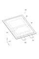
- FIG. 1 is a perspective view of a lithium-ion secondary battery 100 according to an embodiment.
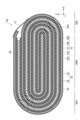
- FIG. 2 is a cross-sectional view of a laminate 90 according to one embodiment.
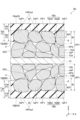
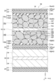
- FIG. 2 is an enlarged cross-sectional view of a laminate 90 according to one embodiment.
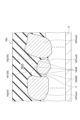
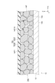
- FIG. 2 is an enlarged cross-sectional view of a negative electrode according to one embodiment.
- FIG. 4 is an enlarged cross-sectional view of a negative electrode according to another embodiment.
- FIG. 4 is an enlarged cross-sectional view of a negative electrode according to another embodiment.
- FIG. 4 is an enlarged cross-sectional view of a negative electrode according to another embodiment.
- FIG. 4 is an enlarged cross-sectional view of a negative electrode according to another embodiment.
- FIG. 4 is an enlarged cross-sectional view of a negative electrode according to another embodiment.
- FIG. 4 is an enlarged cross-sectional view of a negative electrode according to another embodiment.
- FIG. 4 is an enlarged cross-sectional view of
- FIG. 4 is an enlarged cross-sectional view of a negative electrode according to another embodiment.
- FIG. 11 is an enlarged cross-sectional view of a laminate according to another embodiment.
- FIG. 11 is an enlarged cross-sectional view of a laminate according to another embodiment.
- FIG. 11 is an enlarged cross-sectional view of a curved portion of a laminate according to another embodiment.
- FIG. 11 is a cross-sectional view of a lithium-ion secondary battery according to another embodiment.
- FIG. 11 is a cross-sectional view of a lithium-ion secondary battery according to another embodiment.
- element A when element A is said to "connect" element B, it should be understood that element A may be directly connected to element B, or there may be an intermediate element C such that elements A and B are indirectly connected to one another.
- spatially related terms such as “above” may be used herein for ease of description to describe the relationship of an element or feature to another element(s) or feature(s) as illustrated in the figures. It should be understood that the spatially related terms are intended to include different orientations of the device or equipment in use or operation in addition to the orientation depicted in the figures. For example, if the device in the figures is turned over, elements described as being “above” or “on” the other elements or features would be oriented “below” or “below” the other elements or features. Thus, the exemplary term “above” can include both an orientation of above and below.
- first, second, third, etc. may be used herein to describe various elements, components, regions, layers, and/or portions, but it should be understood that these elements, components, regions, layers, and/or portions should not be limited by these terms. These terms are used to distinguish one element, component, region, layer, or portion from another. Thus, a first element, component, region, layer, or portion described below can be referred to as a second element, component, region, layer, or portion without departing from the teachings of the exemplary embodiments.
- the energy storage element 100 includes a case 80 and a laminate 90 housed in the case 80. Leads 101 and 102 are connected to the laminate 90 and are drawn out from the inside of the case 80 to the outside.
- the material of the case 80 may be a resin sheet, a resin-coated metal sheet, or the like.
- the axial direction of the winding of the laminate 90 is defined as the Y direction
- the thickness direction of the laminate 90 (the direction perpendicular to the Y direction and in which the thickness of the laminate 90 is the thinnest) is defined as the Z' direction (first direction)
- the direction perpendicular to the Y direction and Z' direction is defined as the X' direction.
- the laminate 90 has a negative electrode 10, a positive electrode 30, and a separator 20, and the negative electrode 10, the positive electrode 30, and the separator 20 are wound with the separator 20 interposed between the negative electrode 10 and the positive electrode 30.
- the wound ends of the laminate 90 are fixed with tape 13.
- the negative electrode 10, the positive electrode 30, and the separator 20 are each sheet-shaped.
- the laminate 90 has a flat portion 90M where the laminate of the positive electrode 30, the separator 20, and the negative electrode 10 is flat, and curved portions 90C where the laminate of the positive electrode 30, the separator 20, and the negative electrode 10 is curved, which are arranged at both ends of the flat portion 90M.
- the laminate 90 is wound so as to have alternating flat portions 90M and curved portions 90C.
- the positive electrode 30 has a second conductor 32 and a positive electrode active material layer 34
- the negative electrode 10 has mainly a first conductor 12 and a first active material layer 14.
- the negative electrode 10 has a first conductor 12, a first active material layer 14 ⁇ provided on the first surface 12a of the first conductor 12, a first layer 16 ⁇ sandwiching the first active material layer 14 ⁇ together with the first conductor 12, a second active material layer 14 ⁇ provided on the second surface 12b of the first conductor 12, and a second layer 16 ⁇ sandwiching the second active material layer 14 ⁇ together with the first conductor 12.
- the main surface of the first layer 16 ⁇ of the negative electrode 10 is in contact with the main surface of the separator 20.
- the main surface of the second layer 16 ⁇ of the negative electrode 10 is in contact with the main surface of the separator 20.
- the Z direction is the direction (first direction) in which the first active material layer 14 ⁇ and the first conductor 12 are aligned, and can also be said to be the direction perpendicular to the first surface 12a of the first conductor 12.
- the Z direction is also the direction (second direction) in which the second active material layer 14 ⁇ and the first conductor 12 are aligned, and can also be said to be the direction perpendicular to the second surface 12b of the first conductor 12.
- the X direction is perpendicular to the Y and Z directions.
- a cross section is a cross section taken along the Z direction unless otherwise defined. 3 to 10, the vertical direction is the Z direction, and the horizontal direction is the X direction.
- the first conductor 12 is, for example, a thin metal plate (metal foil) made of copper, nickel, stainless steel, or an alloy thereof, and is a conductive plate material.
- the thickness of the first conductor 12 can be, for example, 5 to 20 ⁇ m.
- the first active material layer 14 ⁇ includes a plurality of negative electrode active material particles (first negative electrode active material particles) 14P
- the second active material layer 14 ⁇ includes a plurality of negative electrode active material particles (second negative electrode active material particles) 14P.
- the negative electrode active material may be any material capable of absorbing and releasing (intercalating and deintercalating, or doping and dedoping) lithium ions. Examples of the negative electrode active material particles 14P include carbon materials.
- the negative electrode active material particles (second negative electrode active material particles) 14P of layer 14 ⁇ may be the same as or different from each other.
- Examples of carbon materials used for the negative electrode active material particles 14P include graphite, non-graphitizable carbon, easily graphitizable carbon, and low-temperature fired carbon.
- metals used for the negative electrode active material particles 14P are metals that can combine with lithium, such as Al and Sn.
- An example of a semimetal used for the negative electrode active material particles 14P is Si.
- metal oxides used for the negative electrode active material particles 14P are TiO 2 , SnO 2 , and lithium titanate (Li 4 Ti 5 O 12 ).
- An example of the semi-metal oxide used for the negative electrode active material particles 14P is SiO x (0 ⁇ x ⁇ 2).
- the arrangement of the negative electrode active material particles 14P may be random.
- the particle size of the negative electrode active material particles 14P may be 2 to 20 ⁇ m in D50 of the number-based distribution of the diameter of circles equivalent to the area in the cross-sectional images of the first active material layer 14 ⁇ and the second active material layer 14 ⁇ .
- the first active material layer 14 ⁇ and the second active material layer 14 ⁇ may contain an organic compound 14B such as a polymer.
- the organic compound can bond the negative electrode active material particles 14P together and/or the negative electrode active material particles 14P and the first conductor 12.
- the area with the narrowest hatching that extends from the upper left to the lower right corresponds to the organic compound 14B.
- organic compound 14B examples include fluororesins such as polyvinylidene fluoride (PVDF) and polytetrafluoroethylene (PTFE).
- PVDF polyvinylidene fluoride
- PTFE polytetrafluoroethylene
- Other examples of organic compounds include cellulose, styrene-butadiene rubber, ethylene-propylene rubber, acrylic resin, polyimide resin, polyamide-imide resin, etc.
- the organic compound may be an electronically conductive conductive polymer or an ionically conductive conductive polymer.
- An example of an electronically conductive conductive polymer is polyacetylene.
- the organic compound also functions as a conductive assistant particle, so that a conductive assistant does not need to be added.
- an ionically conductive conductive polymer for example, one having ion conductivity such as lithium ions can be used, and examples thereof include a composite of a monomer of a polymer compound (polyether-based polymer compounds such as polyethylene oxide and polypropylene oxide, polyphosphazene, etc.) and a lithium salt such as LiClO 4 , LiBF 4 , LiPF 6 or an alkali metal salt mainly composed of lithium.
- the polymerization initiator used for the composite include a photopolymerization initiator or a thermal polymerization initiator that is compatible with the above-mentioned monomer.
- the amount of organic compound added may be 2 to 20% by mass relative to the mass of the negative electrode active material particles.
- the first active material layer 14 ⁇ and the second active material layer 14 ⁇ may further contain a negative electrode conductive assistant 14F.
- a known conductive assistant may be used as the negative electrode conductive assistant.
- the conductive assistant include carbon-based materials such as graphite, carbon black, and acetylene black, metal fine powders such as copper, nickel, stainless steel, and iron, mixtures of carbon materials and metal fine powders, and conductive oxides such as ITO.
- the amount of the negative electrode conductive assistant added may be 0.5 to 5 mass% with respect to the mass of the negative electrode active material particles. In Figs. 3, 6, and 9 to 11, the hatched area extending from the upper right to the lower left and having the narrowest spacing corresponds to the negative electrode conductive assistant 14F.
- the thickness of the first active material layer 14 ⁇ and the second active material layer 14 ⁇ can be 5 to 300 ⁇ m, and may be the same or different.
- FIG. 4A shows an example of an enlarged cross-sectional view of the negative electrode 10 of the flat portion 90M of the laminate 90 in FIG. 2.
- the thickness of the first active material layer 14 ⁇ is defined as the arithmetic average of the distance DPP1 from the point PP1 farthest from the first conductor 12 in the Z direction to the first conductor 12 among the negative electrode active material particles 14Pout exposed on the opposite side to the first conductor 12 included in the first active material layer 14 ⁇ in the cross-sectional image along the Z direction of the negative electrode exemplified in FIG. 4A for all the negative electrode active material particles 14Pout exposed on the opposite side to the first conductor 12 included in the first active material layer 14 ⁇ in the cross-sectional image.
- the thickness of the second active material layer 14 ⁇ is defined as the arithmetic average of the distance DPP1 from the point PP1 farthest from the first conductor 12 in the Z direction to the first conductor 12 among the negative electrode active material particles 14Pout exposed on the side opposite the first conductor 12 contained in the second active material layer 14 ⁇ in the cross-sectional image along the Z direction of the negative electrode illustrated in Figures 4A and 4B, for all the negative electrode active material particles 14Pout exposed on the side opposite the first conductor 12 contained in the second active material layer 14 ⁇ in the cross-sectional image.
- the magnification of the cross-sectional image can be set so that the number of negative electrode active material particles 14Pout exposed on the side opposite the first conductor 12 contained in each active material layer is approximately 5 to 100.
- the first layer 16 ⁇ has a first portion 16 ⁇ A that is provided across two or more negative electrode active material particles 14Pout (first negative electrode active material particles) exposed on the side opposite the first conductor 12 in the first active material layer 14 ⁇ , and a second portion 16 ⁇ B that penetrates from the first portion 16 ⁇ A between adjacent negative electrode active material particles (first negative electrode active material particles) 14P of the first active material layer 14 ⁇ .
- the second layer 16 ⁇ has a third portion 16 ⁇ A that is provided across two or more negative electrode active material particles 14Pout (second negative electrode active material particles) exposed on the side of the second active material layer 14 ⁇ opposite the first conductor 12, and a fourth portion 16 ⁇ B that penetrates from the third portion 16 ⁇ A into the space between adjacent negative electrode active material particles (second negative electrode active material particles) 14P of the second active material layer 14 ⁇ .
- the space between the negative electrode active material particles (first negative electrode active material particles) 14P where the second portion 16 ⁇ B is arranged refers to an aggregate V of the region sandwiched between any two negative electrode active material particles 14P (first negative electrode active material particles) that may be adjacent in any direction in the first active material layer 14 ⁇ .
- the second portion 16 ⁇ B can extend until it contacts the first conductor 12.
- the first portion 16 ⁇ A is a region of the first layer 16 ⁇ that is separated from the assembly V of the above-mentioned regions.
- the space between the negative electrode active material particles (first negative electrode active material particles) 14P in which the fourth portion 16 ⁇ B is arranged refers to an aggregate V of the region sandwiched between any two negative electrode active material particles 14P (second negative electrode active material particles) that may be adjacent in any direction in the second active material layer 14 ⁇ .
- the third portion 16 ⁇ A is a region of the second layer 16 ⁇ that is separated from the assembly V of the above-mentioned regions.
- the boundary between the first portion 16 ⁇ A and the second portion 16 ⁇ B is exposed on the side opposite the first conductor 12 in the cross section and is formed by a common circumstantial line W of the negative electrode active material particles 14Pout adjacent to each other in a direction perpendicular to the Z direction (e.g., the X direction in Figures 3, 4A, etc.) (see Figure 4A).
- the boundary between the third portion 16 ⁇ A and the fourth portion 16 ⁇ B is exposed on the side opposite the first conductor 12 and is formed by a common circumstantial line W of the negative electrode active material particles 14Pout adjacent to each other in a direction perpendicular to the Z direction (e.g., the X direction in Figures 3, 4A, etc.) (see Figure 4A).
- the boundary between the first part 16 ⁇ A and the second part 16 ⁇ B of the first layer 16 ⁇ has a shape (V-shaped in the figure) formed by the parts of each common circumscribing line W1, W2 that are farthest from the first conductor 12.
- the thickness U of the first portion 16 ⁇ A is the distance of the first portion 16 ⁇ A along the Z direction.
- the thickness U' of the third portion 16 ⁇ A is the distance of the third portion 16 ⁇ A along the Z direction.
- the average thickness Uav of the first portion 16 ⁇ A and the average thickness U'av of the third portion 16 ⁇ A may be 0.1 to 5.0 ⁇ m.
- Uav and U'av may be 0.5 ⁇ m or more, 0.7 ⁇ m or more, or 1.0 ⁇ m or more.
- Uav and U'av may be 4.0 ⁇ m or less, or 3.0 ⁇ m or less.
- the average thickness Uav of the first portion 16 ⁇ A is defined as the area of the first portion 16 ⁇ A that does not penetrate between the negative electrode active material particles 14P of the first active material layer 14 ⁇ , of the first layer 16 ⁇ extracted by image processing in a cross-sectional image of the negative electrode along the Z direction, divided by the length of the first portion 16 ⁇ A in a direction perpendicular to the Z direction in the image (for example, the Z direction in FIG. 3, but in some cross sections it may be the Y direction).
- the magnification of the cross-sectional image can be set so that the length of the first portion 16 ⁇ A in the direction perpendicular to the Z direction is, for example, 50 to 500 ⁇ m.
- the average thickness U'av of the third portion 16 ⁇ A is defined as the area of the third portion 16 ⁇ A that does not penetrate between the negative electrode active material particles 14P of the second active material layer 14 ⁇ , of the second layer 16 ⁇ extracted by image processing in a cross-sectional image of the negative electrode along the Z direction, divided by the length of the third portion 16 ⁇ A in a direction perpendicular to the Z direction in the image.
- the magnification of the cross-sectional image can be set so that the length of the third portion 16 ⁇ A in a direction perpendicular to the Z direction is, for example, 50 to 500 ⁇ m.
- the thickness H of the second portion 16 ⁇ B is the distance of the second portion 16 ⁇ B along the Z direction.
- the thickness H' of the fourth portion 16 ⁇ B is the distance of the fourth portion 16 ⁇ B along the Z direction.
- the average thickness Hav of the second portion 16 ⁇ B is defined as the area of the second portion 16 ⁇ B that penetrates between the negative electrode active material particles 14P of the first active material layer 14 ⁇ of the first layer 16 ⁇ extracted by image processing in a cross-sectional image of one negative electrode, divided by the length of the second portion 16 ⁇ B in the X direction.
- the magnification of the cross-sectional image can be set so that the length of the second portion 16 ⁇ B in the X direction is, for example, 50 to 500 ⁇ m.
- the average thickness H'av of the fourth portion 16 ⁇ B is defined as the area of the fourth portion 16 ⁇ B that penetrates between the negative electrode active material particles 14P of the second active material layer 14 ⁇ of the second layer 16 ⁇ extracted by image processing in a cross-sectional image of one negative electrode, divided by the length of the fourth portion 16 ⁇ B in the X direction.
- the magnification of the cross-sectional image can be set so that the length of the fourth portion 16 ⁇ B in the X direction is, for example, 50 to 500 ⁇ m.
- the average thickness of the fourth portion 16 ⁇ B in one cross-sectional image along the second direction (Z direction) is H'av and the average particle size of the multiple negative electrode active material particles 14P contained in the second active material layer 14 ⁇ in the image is R'av, the relationship 0.3 ⁇ H'av/R'av ⁇ 3.0 is satisfied.
- Rav is the particle size obtained by D50 based on the number of the area circle equivalent diameters of all the negative electrode active material particles contained in the first active material layer 14 ⁇ in one cross-sectional image.
- R'av is the particle size obtained by D50 based on the number of the area circle equivalent diameters of all the negative electrode active material particles contained in the second active material layer 14 ⁇ in one cross-sectional image.
- the number of active material particles measured in one cross-sectional image can be 10 to 1000.
- 0.5 ⁇ Hav/Rav ⁇ 2.0 can be satisfied, Hav/Rav ⁇ 1.5 can be satisfied, Hav/Rav ⁇ 1.3 can be satisfied, 0.5 ⁇ H'av/R'av ⁇ 2.0 can be satisfied, H'av/R'av ⁇ 1.5 can be satisfied, and H'av/R'av ⁇ 1.3 can be satisfied.
- At least one of Hav/Rav and H'av/R'av may be satisfied in one cross-sectional image, but may also be satisfied in multiple cross-sectional images. Specifically, it may be satisfied in two cross-sectional images, it may be satisfied in three cross-sectional images, or it may be satisfied in five cross-sectional images.
- the thickness T of the first layer 16 ⁇ is the distance of the first layer 16 ⁇ along the Z direction.
- the thickness T' of the second layer 16 ⁇ is the distance of the second layer 16 ⁇ along the Z direction.
- the thickness T of the first layer 16 ⁇ is the distance in the Z direction from the surface 16 ⁇ AS of the first layer 16 ⁇ opposite the first conductor 12 to the surface of the second portion 16 ⁇ B that is located on the first conductor 12 side in the Z direction.
- the thickness T' of the second layer 16 ⁇ is the distance in the Z direction from the surface 16 ⁇ AS of the second layer 16 ⁇ opposite the first conductor 12 to the surface of the fourth portion 16 ⁇ B located on the first conductor 12 side in the Z direction.
- the average thickness Tav of the first layer 16 ⁇ is defined as the area of the first layer 16 ⁇ extracted by image processing in a cross-sectional image of one negative electrode divided by the length of the first layer 16 ⁇ in the first direction (X direction).
- the magnification of the cross-sectional image can be set so that the length of the first layer 16 ⁇ in the X direction is, for example, 50 to 500 ⁇ m.
- the average thickness T'av of the second layer 16 ⁇ is defined as the area of the second layer 16 ⁇ extracted by image processing in a cross-sectional image of one negative electrode divided by the length of the second layer 16 ⁇ in the second direction (X direction).
- the magnification of the cross-sectional image can be set so that the length of the second layer 16 ⁇ in the X direction is, for example, 50 to 500 ⁇ m.
- the average thickness Tav of the first layer 16 ⁇ and the average thickness T'av of the second layer 16 ⁇ may be 0.1 to 300 ⁇ m.
- Tav, Uav, Hav, and Hav/Rav may each be a numerical value obtained from one cross-sectional image, or may be the arithmetic average of the numerical values obtained from, for example, three or five cross-sectional images.
- the length L ⁇ BS of the surface 16 ⁇ BS of the first layer 16 ⁇ on the first conductor 12 side is greater than the length L ⁇ AS of the surface 16 ⁇ AS of the first layer 16 ⁇ on the opposite side to the first conductor 12.
- L ⁇ BS/L ⁇ AS may be 1.1 or more, or may be 1.2 or more.
- the length L ⁇ BS of the surface 16 ⁇ BS of the second layer 16 ⁇ on the side of the first conductor 12 is greater than the length L ⁇ AS of the surface 16 ⁇ AS of the second layer 16 ⁇ on the side opposite the first conductor 12.
- L ⁇ BS/L ⁇ AS may be 1.1 or greater, or 1.2 or greater.
- the surface 16 ⁇ BS of the first layer 16 ⁇ facing the first conductor 12 also includes the contact interface between the first layer 16 ⁇ and the negative electrode active material particles 14P.
- the surface 16 ⁇ BS of the second layer 16 ⁇ facing the first conductor 12 includes the contact interface between the second layer 16 ⁇ and the negative electrode active material particles 14P.
- the portion ISO of the second part 16 ⁇ B of the first layer 16 ⁇ that is not connected to the first part 16 ⁇ A and is isolated is excluded from the calculation of the length L ⁇ AS of the surface 16 ⁇ BS.
- the portion ISO of the fourth part 16 ⁇ B of the second layer 16 ⁇ that is not connected to the third part 16 ⁇ A and is isolated is excluded from the calculation of the length L ⁇ BS of the surface 16 ⁇ BS.
- the magnification of the cross-sectional image for obtaining the length of each surface can be set so that the number of negative electrode active material particles 14Pout exposed on the side opposite the first conductor 12 in the cross-sectional image is approximately 5 to 100.
- the length of each surface can be obtained based on the number of pixels constituting each curve and the size of the pixels after extracting curves on both surfaces of the first and second layers based on the difference in composition between the first and second layers and the negative electrode active material particles from the SEM-EDX cross-sectional image.
- the length L ⁇ AS of the surface 16 ⁇ AS of the first layer 16 ⁇ opposite the first conductor 12 may be less than 1.1 or less than 1.05 relative to the length of the first layer 16 ⁇ in a direction perpendicular to the Z direction (the X direction in Figure 3).
- the length L ⁇ AS of the surface 16 ⁇ AS of the second layer 16 ⁇ opposite the first conductor 12 may be less than 1.1 or less than 1.05 relative to the length of the second layer 16 ⁇ in a direction perpendicular to the Z direction (the X direction in FIG. 3).
- the ratio of the length of the surface 16 ⁇ AS of the first layer 16 ⁇ to the length of the first layer 16 ⁇ in a direction perpendicular to the Z direction may be less than 1.1 or less than 1.05, while the ratio of the length of the surface 16 ⁇ AS of the second layer 16 ⁇ to the length of the second layer 16 ⁇ in a direction perpendicular to the Z direction (X direction in FIG. 3) may be 1.1 or more or 1.2 or more. Conversely, the ratio of the length of the surface 16 ⁇ AS of the first layer 16 ⁇ to the length of the first layer 16 ⁇ in a direction perpendicular to the Z direction (X direction in FIG.
- 3) may be 1.1 or more or 1.2 or more, while the ratio of the length of the surface 16 ⁇ AS of the second layer 16 ⁇ to the length of the second layer 16 ⁇ in a direction perpendicular to the Z direction (X direction in FIG. 3) may be less than 1.1 or less than 1.05.
- a gap VV may be formed between the separator 20 and the surface 16 ⁇ AS of the first layer 16 ⁇ or the surface 16 ⁇ AS of the second layer 16 ⁇ , whichever has a larger ratio to the above length.
- the surface 16 ⁇ As of the first layer 16 ⁇ or the surface 16 ⁇ As of the second layer 16 ⁇ , whichever has a larger ratio to the above length, may be on the inside or outside of the winding.
- the inside of the winding refers to the side closer to the winding axis, and the outside of the winding refers to the side farther from the winding axis.
- the second portion 16 ⁇ B of the first layer 16 ⁇ includes a portion extending from the first portion 16 ⁇ A to a position that exceeds a length dp/2 that is half the particle diameter dp of at least one negative electrode active material particle 14P1 (first negative electrode active material particle) exposed on the side opposite to the first conductor 12 in the Z direction.
- the particle diameter dp of the negative electrode active material particle is the distance along the first direction (Z direction) between the point PP1 of the negative electrode active material particle 14P1 that is farthest from the first conductor 12 and the point PP2 of the negative electrode active material particle 14P that is closest to the first conductor 12 in a cross-sectional image of the negative electrode 10 along the first direction (Z direction).
- the distance DPP1 in the first direction (Z direction) between the first surface 12a of the first conductor 12 and the point PP1 of the negative electrode active material particle 14P that is farthest from the first conductor 12 may be different for each negative electrode active material particle 14P.
- the distance DPP1 in the first direction (Z direction) between the second surface 12b of the first conductor 12 and the point PP1 of the negative electrode active material particle 14P that is farthest from the first conductor 12 may be different for each negative electrode active material particle 14P.
- the second part 16 ⁇ B extending to a position exceeding dp/2, which is half the length of the particle diameter dp, means that the second part 16 ⁇ B exceeds, in the Z direction, a line A that passes through a point where half the particle diameter (dp/2) of the negative electrode active material particle 14P1 is located and runs in the X direction perpendicular to the Z direction, on at least one side of the X direction of the negative electrode active material particle P1.
- the second part 16 ⁇ B extends across the line A from the first part 16 ⁇ A in the Z direction.
- the fourth portion 16 ⁇ B of the second layer 16 ⁇ includes a portion that extends from the third portion 16 ⁇ A to a position that exceeds a length dp/2 that is half the particle diameter dp of at least one negative electrode active material particle 14P1 (second negative electrode active material particle) exposed on the side opposite to the first conductor 12 in the Z direction.
- the fourth part 16 ⁇ B of the second layer 16 ⁇ extends to a position exceeding dp/2, which is half the length of the particle diameter dp, means that the fourth part 16 ⁇ B exceeds, in the Z direction, a line A that passes through a point where it is half the particle diameter (dp/2) of the negative electrode active material particle 14P1 and that runs in the X direction perpendicular to the Z direction, on at least one side of the X direction of the negative electrode active material particle P1.
- the fourth part 16 ⁇ B extends across the line A from the third part 16 ⁇ A in the Z direction.
- the thickness and average thickness of the first conductor 12, first active material layer 14 ⁇ , second active material layer 14 ⁇ , first layer 16 ⁇ , second layer 16 ⁇ constituting the negative electrode 10, the second conductor 32 constituting the positive electrode 30, and the positive electrode active material layer 34 are the same in the flat portion 90M shown in FIG. 2 and the curved portion 90C.
- the second portion 16 ⁇ B of the first layer 16 ⁇ extends from the first portion 16 ⁇ A to a position covering a point PP2 closest to the first conductor 12 of at least one negative electrode active material particle 14P1 exposed on the side opposite the first conductor in the first direction (Z direction), and extends beyond point PP2 in the Z direction.
- the fourth portion 16 ⁇ B of the second layer 16 ⁇ extends from the third portion 16 ⁇ A to a position covering a point PP2 closest to the first conductor 12 of at least one negative electrode active material particle 14P2 exposed on the side opposite the first conductor in the second direction (Z direction), and extends beyond point PP2 in the Z direction.
- the first layer 16 ⁇ is provided for the first active material layer 14 ⁇
- the second layer 16 ⁇ is provided for the second active material layer 14 ⁇ .
- the negative electrode 10 may have only either the first layer 16 ⁇ or the second layer 16 ⁇ .
- the negative electrode 10 has a first active material layer 14 ⁇ and a second active material layer 14 ⁇ on both sides of the first conductor 12, respectively.
- the negative electrode 10 may have either the first layer 16 ⁇ or the second layer 16 ⁇ .
- the first layer 16 ⁇ and the second layer 16 ⁇ contain an inorganic material.
- An example of the inorganic material is an inorganic compound.
- An example of the inorganic compound is a metal oxide or a metal hydroxide.
- An example of the metal oxide is one or more metal oxides selected from aluminum oxide, magnesia, titania, silica, zirconia, zinc oxide, iron oxide, ceria, yttria, etc., which are prepared in a particulate form.
- An example of the metal hydroxide is magnesium hydroxide.
- An example of the aluminum oxide is alumina (Al 2 O 3 ), alumite (Al 2 O 3.3H 2 O), and boehmite (Al 2 O 3.5H 2 O).
- Preferred inorganic materials are alumina, boehmite, magnesia, and magnesium hydroxide.
- the inorganic material may be a plurality of particles.
- the inorganic material particles may have an average particle size defined by D50 of the volume-based particle size distribution of laser diffraction of 10 to 1000 nm.
- the first layer 16 ⁇ and the second layer 16 ⁇ may further contain an organic compound.
- An example of the organic compound is a polymer compound containing fluorine, such as polyvinylidene fluoride (PVdF).
- PVdF polyvinylidene fluoride
- the organic compound can function as a binder that bonds inorganic material particles together and between the inorganic material particles and the negative electrode active material particles.
- the mass ratio of the inorganic compound to the organic compound in the first layer 16 ⁇ and the second layer 16 ⁇ may be 1:1 to 100:1.
- the positive electrode 30 has a plate-shaped second conductor 32 and a positive electrode active material layer 34 provided on one or both surfaces of the second conductor 32 .
- the second conductor 32 may be, for example, a thin metal plate (metal foil) made of aluminum, copper, nickel, or an alloy thereof.
- the positive electrode active material layer 34 may mainly comprise positive electrode active material particles, a positive electrode binder, and an appropriate amount of a conductive assistant.
- the positive electrode active material is not particularly limited as long as it is capable of reversibly absorbing and releasing lithium ions, desorbing and inserting lithium ions (intercalating them), or doping and dedoping lithium ions with their counter anions (e.g., ClO 4 ⁇ ), and any known active material can be used.
- lithium cobalt oxide LiCoO2
- lithium nickel oxide LiNiO2
- lithium manganese spinel LiMn2O4
- M is one or more elements selected from Al, Mg, Nb, Ti, Cu, Zn, Cr ), lithium vanadium compound ( LiV2O5 ), olivine type LiMPO4 (wherein M is one or more elements selected from Co, Ni, Mn, Fe, Mg, Nb, Ti, Al, Zr, or VO), lithium titanate (Li4Ti5O12 ) , LiNi x Co
- the composite metal oxide include composite metal oxides such as yAlzO2 (0.9 ⁇ x + y+z ⁇
- the positive electrode active material layer 34 may contain an organic compound.
- the organic compound may function as a binder that bonds the active materials together and also bonds the active materials and the second conductor 32.
- the organic compound may be any compound capable of the above-mentioned bonding, and may be, for example, a fluororesin such as polyvinylidene fluoride (PVDF) or polytetrafluoroethylene (PTFE).
- PVDF polyvinylidene fluoride
- PTFE polytetrafluoroethylene
- cellulose, styrene-butadiene rubber, ethylene-propylene rubber, acrylic resin, polyimide resin, polyamide-imide resin, or the like may be used as the binder.
- the amount of organic compound contained in the positive electrode active material layer 34 is not particularly limited, but if added, it is preferably 0.5 to 5 mass % relative to the mass of the active material.
- the positive electrode active material layer 34 may contain a conductive assistant.
- the conductive assistant is not particularly limited as long as it improves the conductivity of the positive electrode active material layer 34, and the above-mentioned negative electrode conductive assistants can be used.
- the amount of conductive additive contained in the positive electrode active material layer 34 is not particularly limited, but if added, it may be 0.5 to 5 mass % relative to the mass of the active material.
- Separator 20 There is no particular limitation on the material of the separator 20.
- An example of the separator has a main layer 22 which is generally a porous sheet of polyolefin such as polyethylene or polypropylene, or a nonwoven fabric.
- the thickness of the main layer 22 may be 3.0 to 30 ⁇ m.
- the separator 20 may have an inorganic compound-containing layer 21 on the side of the main layer 22 that comes into contact with the positive electrode active material layer 34.
- Examples of the inorganic compound in the inorganic compound-containing layer 21 are the same as those given for the first layer 16 ⁇ , and may be, for example, alumina particles.
- the inorganic compound-containing layer 21 may have an organic compound that functions as a binder. Examples of the organic compound are the same as those given for the first layer 16 ⁇ .
- the thickness of the main layer 22 may be 3.0 to 30 ⁇ m.
- a laminate 90 having a separator/positive electrode 30/separator/negative electrode 10 structure is wound so that the separator 20 is interposed between the positive electrode 30 and the negative electrode 10.
- each positive electrode active material layer 34 of the positive electrode 30 is in contact with the second conductor 32, and the other main surface of each positive electrode active material layer 34 is in contact with the main surface of the separator 20.
- the main surface of the first active material layer 14 ⁇ of the negative electrode 10 opposite the first layer 16 ⁇ is in contact with the main surface of the first conductor 12.
- the surface of the first layer 16 ⁇ of the negative electrode 10 opposite the first active material layer 14 ⁇ is in contact with the main surface of the separator 20.
- the surface of the second active material layer 14 ⁇ of the negative electrode 10 opposite the second layer 16 ⁇ is in contact with the first conductor 12.
- the surface of the second layer 16 ⁇ of the negative electrode 10 opposite the second active material layer 14 ⁇ is in contact with the separator 20.
- each layer is stacked in the Z direction.
- the lead 101 shown in FIG. 1 is connected to the portion of the second conductor 32 exposed from the positive electrode active material layer 34.
- the lead 102 is connected to the portion of the first conductor 12 exposed from the first active material layer 14 ⁇ or the second active material layer 14 ⁇ .
- the leads 101 and 102 extend from the inside to the outside of the case 80.
- the first layer 16 ⁇ of the negative electrode 10 and the main layer 22 of the separator 20 are in contact.
- the positive electrode active material layer 34 of the positive electrode 30 and the inorganic compound-containing layer 21 of the separator 20 are in contact.
- a laminate having a first active material layer 14 ⁇ and a second active material layer 14 ⁇ formed on both sides of a first conductor 12 is prepared by a conventionally known method.
- the inorganic particles, binder, and solvent are mixed to prepare a slurry for forming the first layer.
- the slurry for forming the first layer is then applied onto at least one of the first active material layer 14 ⁇ and the second active material layer 14 ⁇ , and then dried at high temperature for a predetermined time.
- the slurry for forming the second layer may be applied separately from the slurry for forming the first layer.
- the first layer 16 ⁇ and/or the second layer 16 ⁇ are more likely to penetrate between the negative electrode active material particles.
- the drying time under reduced pressure is increased, the first layer 16 ⁇ and/or the second layer 16 ⁇ are more likely to penetrate between the negative electrode active material particles.
- the negative electrode is pressed after the formation of the first layer 16 ⁇ and/or the second layer 16 ⁇ , the first layer 16 ⁇ and/or the second layer 16 ⁇ are more likely to penetrate between the negative electrode active material particles.
- FIG. 7 is a cross-sectional view of the negative electrode 10 according to another embodiment. In this embodiment, only the structure on one side of the first conductor 12 is shown, and the structure on the other side is omitted.
- a part 14P1S of each surface of the negative electrode active material particle 14P1 exposed on the side opposite to the first conductor 12 is flattened. This form is easily obtained by pressing each surface of the negative electrode active material particle 14P1 before forming the first layer 16. In this embodiment, there is an effect of reducing the possibility that the negative electrode active material particle 14P that is not covered by the first layer 16 ⁇ is generated.
- the protrusion may protrude from the first layer 16 ⁇ . If there are any areas of the negative electrode active material particles that are not covered, the difference in resistance between the first layer 16 ⁇ and the first active material layer 14 ⁇ will cause current to concentrate in areas of the first active material layer 14 ⁇ where the first layer 16 ⁇ is not present, increasing the utilization rate of only those areas, resulting in variation in deterioration within the first active material layer 14 ⁇ and possibly reducing the cycle characteristics.
- FIG. 8 is a cross-sectional view of a negative electrode according to another embodiment.
- the negative electrode active material particles 14P are aligned in the in-plane direction in the first active material layer 14 ⁇ .
- the negative electrode 10 may be wound so that the second layer 16 ⁇ is positioned on the outer side of the winding than the first layer 16 ⁇ , but the second layer 16 ⁇ may also be wound so that it is positioned on the inner side of the winding than the first layer 16 ⁇ .
- the inner side of the winding means the side closer to the winding axis, and the outer side of the winding means the side farther from the winding axis.
- the third portion 16 ⁇ A of the second layer 16 ⁇ on the inner side of the winding which has a relatively smaller radius of curvature, can be made thinner, and the adhesion with the opposing positive electrode is improved, thereby improving the high-temperature cycle characteristics.
- the difference between the average thicknesses Uav and U'av of the first portion 16 ⁇ A and the third portion 16 ⁇ A may be 0 to 2.0 ⁇ m.
- FIG. 10 is an enlarged view of a laminate 90 according to another embodiment.
- the average thickness T'av of the second layer 16 ⁇ is smaller than the average thickness Tav of the first layer 16 ⁇ on the outer side of the winding.
- the negative electrode 10 may be wound so that the second layer 16 ⁇ is positioned on the outer side of the winding than the first layer 16 ⁇ , but may also be wound so that the second layer 16 ⁇ is positioned on the inner side of the winding than the first layer 16 ⁇ .
- the inner side of the winding means the side closer to the winding axis, and the outer side of the winding means the side farther from the winding axis.
- the average thickness T'av of the second layer 16 ⁇ on the inner side of the winding can be made thinner, and the adhesion with the opposing positive electrode is improved, thereby improving the high-temperature cycle characteristics.
- the difference between the average thicknesses Tav and T'av of the first layer 16 ⁇ and the second layer 16 ⁇ may be 0 to 2.0 ⁇ m.
- the average thickness U'av of the third portion 16 ⁇ A is smaller than the average thickness Uav of the first portion 16 ⁇ A
- the average thickness H'av of the fourth portion 16 ⁇ B is smaller than the average thickness Hav of the second portion 16 ⁇ B.
- the average thickness U'av of the third portion 16 ⁇ A is smaller than the average thickness Uav of the first portion 16 ⁇ A
- the average thickness H'av of the fourth portion 16 ⁇ B is the same as the average thickness Hav of the second portion 16 ⁇ B.
- the average thickness T'av of the third portion 16 ⁇ A is the same as the average thickness Tav of the first portion 16 ⁇ A, and the average thickness H'av of the fourth portion 16 ⁇ B is smaller than the average thickness Hav of the second portion 16 ⁇ B.
- the difference between the average thickness Hav of the second portion 16 ⁇ B and the average thickness H'av of the fourth portion 16 ⁇ B may be 0 to 2.0 ⁇ m.
- the difference between the average thickness Uav of the first portion 16 ⁇ A and the average thickness U'av of the third portion 16 ⁇ A may be 0 to 4.0 ⁇ m.
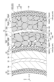
- FIG. 11 is an enlarged cross-sectional view of a curved portion 90C of a laminate 90 according to another embodiment.
- the Z direction which is the direction (first direction) in which the first active material layer 14 ⁇ and the first conductor 12 are aligned, is the radial direction of the curved portion 90C.
- the X, Y, and Z directions shown in FIG. 11 are the directions at the center of the laminate 90 in the vertical direction, that is, when the radial direction of the curved portion is horizontal.
- the average thickness Tav-c of the first layer 16 ⁇ of the curved portion 90C shown in FIG. 11 is smaller than the average thickness Tav (see FIG. 4A) of the first layer 16 ⁇ of the flat portion 90M shown in FIG. 3.
- the average thickness T'av-c of the second layer 16 ⁇ of the curved curved portion 90C in FIG. 11 is smaller than the average thickness T'av of the second layer 16 ⁇ of the flat portion 90M in FIG. 3 (see FIG. 4A).
- the average thickness Tav-c of the first layer 16 ⁇ of the curved portion 90C in FIG. 11 is smaller than the average thickness Tav of the first layer 16 ⁇ of the flat portion 90M, and the average thickness T'av-c of the second layer 16 ⁇ of the curved portion 90C is smaller than the average thickness T'av of the second layer 16 ⁇ of the flat portion 90M.
- the high-temperature cycle characteristics are improved by improving the adhesion with the opposing positive electrode.
- the difference between the average thickness Tav and the average thickness Tav-c, and the difference between the average thickness T'av and the average thickness T'av-c may each be 0 to 2.0 ⁇ m.
- the average thickness Tav-c of the first layer 16 ⁇ and the average thickness T'av-c of the second layer 16 ⁇ in the cross-sectional image of the curved portion are obtained by dividing the area of the first layer 16 ⁇ by the length of the first layer 16 ⁇ along the surface of the separator 20 facing the first layer 16 ⁇ , and by dividing the area of the second layer 16 ⁇ by the length of the second layer 16 ⁇ along the surface of the separator 20 facing the second layer 16 ⁇ .
- FIG. 12 is a cross-sectional view showing an example in which a laminate 90 having a negative electrode 10, a separator 20, and a positive electrode 30 is wound into a cylindrical shape and housed in a case 80.
- the case 80 includes a metal can 81, a gasket 83, and an electrode lead 82.
- the axis of winding is the Y direction
- the horizontal direction is the Z direction in which the first active material layer 14 ⁇ and the first conductor 12 are aligned
- the X direction is the direction perpendicular to the Y and X directions.
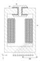
- FIG. 13 shows a stacked type energy storage element in which multiple negative electrodes 10 and multiple positive electrodes 30 are stacked with a separator 20 interposed between each positive electrode 30 and negative electrode 10.
- the direction in which the first active material layer 14 ⁇ and the first conductor 12 are aligned is the Z direction, and the X direction and Y direction are perpendicular to the Z direction.
- the first layer 16 ⁇ and part of the second layer 16 ⁇ which are made of inorganic material, cover the gaps between the negative electrode active material particles, thereby reducing the surface roughness on the outer surface of the negative electrode 10 and reducing the resistance at the interface between the negative electrode 10 and the separator 20.
- the groove-like parts formed by the negative electrode active material particles 14P current concentration during charging is alleviated and the generation of dendrites is suppressed, making it possible to cycle stably even at high temperatures.
- Example 1 Example in which the first layer is present only in the first active material layer 14 ⁇
- Preparation of Positive Electrode The positive electrode active material particles, the conductive material, and the binder were mixed to prepare a positive electrode mixture.
- the positive electrode active material was lithium cobalt oxide (LiCoO 2 : hereinafter, abbreviated as LCO when described below), the conductive material was carbon black, and the binder was polyvinylidene fluoride (PVDF).
- the positive electrode active material particles, the conductive material, and the binder were in a mass ratio of 96:2:2.
- the positive electrode mixture was dispersed in N-methyl-2-pyrrolidone (NMP) to prepare a positive electrode slurry.
- NMP N-methyl-2-pyrrolidone
- the positive electrode slurry was applied to one side of an aluminum foil having a thickness of 15 ⁇ m as a second conductor so that the weight per unit area after drying was about 20.0 mg/cm 2.
- the positive electrode slurry was dried at 100° C. to remove the solvent, and a positive electrode active material layer was formed on one side of the aluminum foil.
- the positive electrode slurry was applied to the other side of the aluminum foil so that the weight per unit area after drying was about 10.0 mg/cm 2 .
- the aluminum foil was dried at 100° C. to remove the solvent, and a positive electrode active material layer was formed on both sides of the aluminum foil. After the positive electrode active material layers were formed on both sides of the second conductor, the positive electrode was obtained by pressing at 1000 kgf/cm.
- a negative electrode active material particle, a conductive material, and a binder were mixed to prepare a negative electrode mixture.
- the negative electrode active material was graphite, and the binder was polyvinylidene fluoride (PVDF).
- PVDF polyvinylidene fluoride
- the negative electrode active material particle and the binder were in a mass ratio of 95:5.
- This negative electrode mixture was dispersed in N-methyl-2-pyrrolidone (NMP) to prepare a negative electrode slurry. Then, the negative electrode slurry was applied to one side of a copper foil having a thickness of 10 ⁇ m as a first conductor so that the weight per unit area after drying was about 6.0 mg/cm 2. After application, the coating was dried at 100° C.
- the negative electrode slurry was applied to the other side of the copper foil so that the weight per unit area after drying was about 10.0 mg/cm 2 .
- the coating was dried at 100° C. to remove the solvent, forming a first active material layer on both sides of the copper foil, and forming a first active material layer on both sides of the first conductor.
- the thickness of the first active material layer was about 50 ⁇ m.
- the inorganic particles and the binder were mixed to prepare a first layer composite material.
- the inorganic particles were alumina (Al 2 O 3 ), and the binder was polyvinylidene fluoride (PVDF).
- PVDF polyvinylidene fluoride
- the mass ratio of the inorganic particles to the binder was 95:5.
- This first layer composite material was dispersed in N-methyl-2-pyrrolidone (NMP) to prepare a first layer slurry.
- NMP N-methyl-2-pyrrolidone
- the obtained slurry for the first layer was applied to one surface of the first active material layer formed on the first conductor using an applicator, with the thickness adjusted to 30 ⁇ m. After application, the slurry was dried under reduced pressure at 90°C for 12 hours. After drying under reduced pressure, the negative electrode of Example 1 was obtained by pressing at 300 kgf/cm.
- Cross-section SEM observation of negative electrode The cross-section of the negative electrode was observed using a cross-sectional SEM image of the obtained negative electrode.
- Cross-sectional SEM observation was performed in five fields of view from the obtained negative electrode, and the average thickness Tav of the first layer and the second layer, the average thickness Uav of the first portion, the average thickness Hav of the second portion, the average particle diameter Rav and Hav/Rav of the active material, and the state of the first layer and the second layer regions in the negative electrode were observed.
- Example 10 The results of cross-sectional SEM observations were also performed in the following examples and comparative examples, and are shown in the table. Note that in Example 10, the average thickness of the second part was nearly zero, but some second parts were present. In Example 9, the average thickness of the second part was nearly zero, but at least one part was confirmed where the second part extended to a position exceeding half the particle size.
- an uncoated portion having a width of 1 mm where the positive electrode active material layer and the first active material layer were not formed was provided at the end, and a nickel negative electrode lead was attached to the uncoated portion of the negative electrode where the first active material layer was not provided, while in the positive electrode, an aluminum positive electrode lead was attached by an ultrasonic fusion machine to the uncoated portion of the positive electrode where the positive electrode active material layer was not provided.
- the laminate was inserted into an exterior body of aluminum laminate film and heat sealed except for one place on the periphery to form an opening.
- a non-aqueous electrolyte was injected into the exterior body.
- the non-aqueous electrolyte was made by dissolving 1.5 mol/L of lithium hexafluorophosphate (LiPF6) in a solvent that was a mixture of equal amounts of ethylene carbonate (EC) and propylene carbonate (PC).
- EC ethylene carbonate
- PC propylene carbonate
- the cycle characteristics of the lithium ion secondary battery for evaluation thus prepared were evaluated in an environment of 85° C. using a secondary battery charge/discharge tester (manufactured by Hokuto Denko Corporation).
- the cycle characteristics were evaluated by repeating 500 charge/discharge cycles of constant current and constant voltage charging at 0.5 C to 4.35 V and constant current discharging at 1 C to 2.8 V.
- the ratio of the discharge capacity after 500 cycles to the discharge capacity of the first cycle was defined as the capacity retention rate.
- the capacity retention rate to the initial capacity is the discharge capacity at the 500th cycle when the discharge capacity at the initial (first) cycle is set to 100%.
- the reduced pressure drying time was 10 hours for Example 2, 8 hours for Example 3, 5 hours for Example 4, 3 hours for Example 5, 1 hour for Example 6, 30 minutes for Example 7, 10 minutes for Example 8, and 5 minutes for Example 9.
- Example 10 (Production of negative electrode according to Example 10)
- the negative electrode of Example 10 was produced under the same conditions as in Example 1, except that after coating the first layer slurry, drying was not performed under reduced pressure but was performed in the air at 100° C.
- Example 11 (Production of a negative electrode according to Example 11: an example in which a first layer is present on a first active material layer and a second layer is present on a second active material layer)
- the slurry for the first layer was applied to one surface of the first active material layer formed on the first conductor by using an applicator, with a thickness of 20 ⁇ m. After application, the slurry was dried under reduced pressure at 90° C. for 3 hours. After drying under reduced pressure, additional drying was performed in the air at 100° C. to remove the solvent component in the first layer. That is, the drying conditions for the first layer were the same as those in Example 5.
- the slurry for the first layer was applied to the second active material layer (the back side sandwiching the current collector) using an applicator, adjusted to a thickness of 20 ⁇ m. After application, the slurry was dried under reduced pressure at 90°C for 12 hours. Then, the slurry was pressed at 300 kgf/cm to obtain the negative electrode of Example 11 having a second layer in addition to the first layer.
- Negative electrodes of Examples 12 to 20 were produced under the same conditions as in Example 11, except that the time for drying under reduced pressure was changed when the second layer was produced on the second active material layer.
- the reduced pressure drying time was 10 hours for Example 12, 8 hours for Example 13, 5 hours for Example 14, 3 hours for Example 15, 1 hour for Example 16, 30 minutes for Example 17, 10 minutes for Example 18, and 5 minutes for Example 19.
- Example 20 A negative electrode of Example 20 was produced under the same conditions as in Example 11, except that, when producing the second layer, drying was carried out in the air at 100° C. instead of drying under reduced pressure.
- Examples 23 to 32 Examples related to wound bodies (basic method for producing lithium ion secondary batteries for evaluation: Examples 23 to 32)
- the produced negative electrode and positive electrode were punched out into a predetermined long shape (negative electrode: 19 mm x 160 mm, positive electrode: 18 mm x 200 mm), and two polypropylene separators having a thickness of 25 ⁇ m were placed on both sides of the negative electrode, and the positive electrode was laminated on one side of the separator.
- an uncoated portion without an active material layer was formed at the end of the negative electrode, and a nickel negative electrode lead was attached to the uncoated portion of the negative electrode without the negative electrode active material layer.
- an uncoated portion without a positive electrode active material layer was formed at both ends of the positive electrode, and an aluminum positive electrode lead was attached to one end of the uncoated portion of the positive electrode by an ultrasonic fusion machine.
- a wound body was produced by winding the laminate with the surface of the negative electrode in which the positive electrode was not laminated as the inner surface side. At this time, the end with the negative electrode lead was laminated so as to be the inside of the winding, and the end with the positive electrode lead was laminated so as to be the outside of the winding.
- Example 23 A wound body of Example 23 was produced by using a negative electrode prepared under the same conditions as in Example 16, and winding the negative electrode so that the first layer was on the inner side of the winding and the second layer was on the outer side of the winding.
- Example 24 (Production of negative electrode according to Example 24)
- the wound body of Example 24 was produced under the same conditions as Example 23, except that the second layer of the negative electrode was wound on the inner side and the first layer was wound on the outer side.
- Example 25 (Production of negative electrode according to Example 25) A negative electrode manufactured under the same conditions as in Example 15 was used, except that when forming the first and second layers, the thickness of the slurry for the first layer was adjusted to 10 ⁇ m using an applicator, and the first layer of the negative electrode was wound so that it was on the inside of the winding and the second layer was on the outside of the winding, thereby producing the wound body of Example 25.
- Example 26 (Production of negative electrode according to Example 26)
- the wound body of Example 24 was produced under the same conditions as Example 25, except that the second layer of the negative electrode was wound on the inner side and the first layer was wound on the outer side.
- Example 27 (Production of negative electrode according to Example 27) A negative electrode manufactured under the same conditions as in Example 15 was used, except that when forming the first and second layers, the thickness of the slurry for the first layer was adjusted to 5 ⁇ m using an applicator, and the first layer of the negative electrode was wound so that it was on the inside of the winding and the second layer was on the outside of the winding, thereby producing the wound body of Example 27.
- Example 27 (Production of negative electrode according to Example 28)
- the wound body of Example 27 was produced under the same conditions as in Example 27, except that the second layer of the negative electrode was wound on the inside of the winding and the first layer was wound on the outside of the winding.
- Example 29 A negative electrode manufactured under the same conditions as in Example 15 was used, except that when forming the first layer, the thickness of the slurry for the first layer was adjusted to 10 ⁇ m using an applicator, and when forming the second layer, the thickness of the slurry for the first layer was adjusted to 5 ⁇ m using an applicator.
- the negative electrode was wound so that the first layer of the negative electrode was on the inner side of the winding and the second layer was on the outer side of the winding, to produce the wound body of Example 29.
- Example 30 (Production of negative electrode according to Example 30)
- the wound body of Example 30 was produced under the same conditions as those of Example 29, except that the second layer of the negative electrode was wound on the inner side and the first layer was wound on the outer side.
- Example 31 (Production of negative electrode according to Example 31) A negative electrode manufactured under the same conditions as in Example 15 was used, except that when forming the first layer, the thickness of the slurry for the first layer was adjusted to 5 ⁇ m using an applicator, and when forming the second layer, the thickness of the slurry for the first layer was adjusted to 8 ⁇ m using an applicator. The negative electrode was wound so that the first layer of the negative electrode was on the inner side of the winding and the second layer was on the outer side of the winding, to produce the wound body of Example 31.
- Example 32 (Production of negative electrode according to Example 32)
- the wound body of Example 32 was produced under the same conditions as Example 31, except that the second layer of the negative electrode was wound on the inner side of the winding and the first layer was wound on the outer side of the winding.
- the conditions and results are shown in Tables 1 to 3.
Landscapes
- Chemical & Material Sciences (AREA)
- Chemical Kinetics & Catalysis (AREA)
- Electrochemistry (AREA)
- General Chemical & Material Sciences (AREA)
- Engineering & Computer Science (AREA)
- Materials Engineering (AREA)
- Inorganic Chemistry (AREA)
- Manufacturing & Machinery (AREA)
- Battery Electrode And Active Subsutance (AREA)
Abstract
蓄電素子は、第1面及び第1面と反対側を向く第2面を備えた第1導電体と、第1導電体の第1面に設けられ複数の第1負極活物質粒子を含有する第1活物質層と、第1活物質層における第1導電体とは反対側において露出する2以上の第1負極活物質粒子に跨がって設けられた第1部、及び、第1部から第1活物質層の第1負極活物質粒子間に侵入している第2部を有し無機材料を含有する第1層と、を有する負極を備える。
Description
本開示は蓄電素子に関する。
リチウムイオン二次電池は、携帯電話、ノートパソコン等のモバイル機器やハイブリットカー等の動力源としても広く用いられている。また、近年は定置型蓄電装置や電気自動車のようにより大型の電池の需要が増加しており、高容量化と安全性を両立するようなより高い性能が求められている。
引用文献1(WO2018-168075A1)には正極とセパレータとの間にフッ素樹脂および粒子の少なくとも1種を含む中間層を形成し、正極中のフッ素系バインダとして特定のものを用いることでガス発生を抑制し、安全性が向上すること開示されている。
引用文献2(JP2008-506244T)には、電極活性物質の表面に多成分系酸化物コート層を形成することで高容量、長寿命及び安全性が確保可能な電気化学素子が開示されている。
しかしながら、高温使用時における蓄電素子のサイクル特性には改善の余地がある。
[1] 第1面及び前記第1面と反対側を向く第2面を備えた第1導電体と、
前記第1導電体の第1面に設けられ、複数の第1負極活物質粒子を含有する、第1活物質層と、
前記第1活物質層における第1導電体とは反対側において露出する2以上の第1負極活物質粒子に跨がって設けられた第1部、及び、前記第1部から前記第1活物質層の前記第1負極活物質粒子間に侵入している第2部を有し、無機材料を含有する第1層と、を有する負極を備える、蓄電素子。
前記第1導電体の第1面に設けられ、複数の第1負極活物質粒子を含有する、第1活物質層と、
前記第1活物質層における第1導電体とは反対側において露出する2以上の第1負極活物質粒子に跨がって設けられた第1部、及び、前記第1部から前記第1活物質層の前記第1負極活物質粒子間に侵入している第2部を有し、無機材料を含有する第1層と、を有する負極を備える、蓄電素子。
[2]前記第1活物質層と前記第1導電体とが並ぶ第1方向に沿った断面画像において、前記第1層の前記第1導電体側の表面の長さは、前記第1層の前記第1導電体とは反対側の表面の長さよりも大きい、[1]に記載の蓄電素子。
[3]前記第1層の第2部は、前記第1部から、前記第1活物質層と前記第1導電体とが並ぶ第1方向において、前記第1導電体とは反対側において露出する少なくとも1つの前記第1負極活物質粒子の粒径の半分を超える位置まで延在している、[1]又は[2]に記載の蓄電素子。
[4]前記第1層の第2部は、前記第1部から、前記第1活物質層と前記第1導電体とが並ぶ第1方向において、前記第1導電体とは反対側において露出する少なくとも1つの前記第1負極活物質粒子の最も前記第1導電体に近い部分を覆う位置まで延在している、[1]~[3]のいずれか一項に記載の蓄電素子。
[5]前記第1活物質層と前記第1導電体とが並ぶ第1方向に沿った断面画像における前記第1層の第2部の平均厚みをHavとし、
前記第1活物質層に含まれる複数の第1負極活物質粒子の平均粒径をRavとした時に、0.3≦Hav/Rav≦3.0を満たす、[1]~[4]のいずれか一項に記載の蓄電素子。
前記第1活物質層に含まれる複数の第1負極活物質粒子の平均粒径をRavとした時に、0.3≦Hav/Rav≦3.0を満たす、[1]~[4]のいずれか一項に記載の蓄電素子。
[6]複数の前記断面画像において、0.3≦Hav/Rav≦3.0を満たす、[5]に記載の蓄電素子。
[7]0.5≦Hav/Rav≦2.0を満たす、[5]又は[6]に記載の蓄電素子。
[8]前記無機材料が無機化合物である、[1]~[7]のいずれか一項に記載の蓄電素子。
[9]前記無機化合物が酸化アルミニウムを含む、[8]に記載の蓄電素子。
[10]前記第1層は、さらに有機化合物を含む、[1]~[9]のいずれか一項に記載の蓄電素子。
[11]前記有機化合物がフッ素を含む高分子化合物を含む、[10]に記載の蓄電素子。
[12]前記高分子化合物がポリビニリデンフルオライドである、[11]に記載の蓄電素子。
[13]前記無機材料と前記有機化合物の質量比率が1:1~100:1である、[10]~[12]のいずれか一項に記載の蓄電素子。
[14]前記第1活物質層の負極活物質粒子が、炭素材料、金属、金属酸化物、半金属、半金属酸化物のうち少なくとも1を含む、[1]~[13]のいずれか一項に記載の蓄電素子。
[15]前記負極は、
前記第1導電体の第2面に設けられ、複数の第2負極活物質粒子を含有する、第2活物質層と、
前記第2活物質層における第1導電体とは反対側において露出する2以上の前記第2負極活物質粒子に跨がって設けられた第3部、及び、前記第3部から前記第2活物質層の前記第2負極活物質粒子間に侵入している第4部を有し、無機材料を含有する第2層と、をさらに有する、[1]~[14]のいずれか一項に記載の蓄電素子。
前記第1導電体の第2面に設けられ、複数の第2負極活物質粒子を含有する、第2活物質層と、
前記第2活物質層における第1導電体とは反対側において露出する2以上の前記第2負極活物質粒子に跨がって設けられた第3部、及び、前記第3部から前記第2活物質層の前記第2負極活物質粒子間に侵入している第4部を有し、無機材料を含有する第2層と、をさらに有する、[1]~[14]のいずれか一項に記載の蓄電素子。
[16]前記第2層の第3部は、前記第3部から、前記第2活物質層と前記第1導電体とが並ぶ第2方向において、前記第1導電体とは反対側において露出する少なくとも1つの前記第2負極活物質粒子の粒径の半分を超える位置まで延在している、[15]に記載の蓄電素子。
[17]前記第2層の第3部は、前記第3部から、前記第2活物質層と前記第1導電体とが並ぶ第2方向において、前記第1導電体とは反対側において露出する少なくとも1つの前記第2負極活物質粒子の最も前記第1導電体に近い部分を覆う位置まで延在している、[15]に記載の蓄電素子。
[17]前記第2層の第3部は、前記第3部から、前記第2活物質層と前記第1導電体とが並ぶ第2方向において、前記第1導電体とは反対側において露出する少なくとも1つの前記第2負極活物質粒子の最も前記第1導電体に近い部分を覆う位置まで延在している、[15]に記載の蓄電素子。
[18]前記第1層の第1部の前記第1活物質層と前記第1導電体とが並ぶ第1方向における厚みと、前記第2層の第3部の前記第2活物質層と前記第1導電体とが並ぶ第2方向における厚みとは、互いに異なる、[15]~[17]のいずれか一項に記載の蓄電素子。
[19]前記第1層の第1部の前記第1活物質層と前記第1導電体とが並ぶ第1方向における厚みは、前記第2層の第3部の前記第2活物質層と前記第1導電体とが並ぶ第2方向における厚みよりも大きい、[15]~[18]のいずれか一項に記載の蓄電素子。
[20]さらに、正極と、前記負極と前記正極との間に配置されたセパレータと、を備える、[1]~[19]のいずれか一項に記載の蓄電素子。
[21]さらに、正極と、前記負極と前記正極との間に配置されたセパレータと、を備え、前記負極、前記セパレータ、及び、前記正極を有する積層体が巻回された、[15]~[19]のいずれか一項に記載の蓄電素子。
[22]前記積層体は、前記第2層が前記第1層よりも内側となるように巻回された、[21]に記載の蓄電素子。
[23]前記第2層の厚みは、前記第1層の厚みよりも小さい、[22]に記載の蓄電素子。
[24]前記積層体は、平坦部と、湾曲部とを交互に有するように巻回され、前記湾曲部の第1層の厚さは、前記平坦部の第1層の厚さよりも薄い、[21]に記載の蓄電素子。
本開示によれば、高温使用時におけるサイクル特性に優れたリチウムイオン二次電池などの蓄電素子が提供される。
以下、本開示の実施形態における技術的解決策を明確かつ詳細に説明するが、説明した実施形態は本開示の実施形態の一部であり、その全てではないことは明らかである。特に定義しない限り、本明細書で使用されるすべての技術用語および科学用語は、本願に属する当業者によって一般的に理解されるのと同じ意味を有する。本願明細書において使用される用語は、特定の実施形態を説明する目的でのみ使用され、本願を限定することを意図するものではない。
以下では、本開示の実施形態について詳細に説明する。しかしながら、本開示は、多くの異なる形態で具現化される可能性があり、本明細書で説明する例示的な実施形態に限定されると解釈されるべきではない。
さらに、添付の図面において、様々な構成要素、層の寸法または厚さは、簡潔かつ明確にするために拡大されている場合がある。本文中では、同じ数値は同じ要素を指す。本明細書で使用される場合、用語「および/または」は、関連する列挙された項目の1つまたは複数の任意のおよびすべての組み合わせを含む。
さらに、要素Aが要素Bを「接続する」と称される場合、要素Aは要素Bに直接接続されてもよいし、中間要素Cが存在し、要素Aと要素Bが互いに間接的に接続されてもよいことを理解されたい。
本明細書で使用される用語は、特定の実施形態を説明するためのものであり、本願を限定することを意図するものではない。
本明細書で使用されるように、単数形は、文脈が明確にそうでないことを示さない限り、複数形も含むことを意図している。
本明細書で使用される場合、用語「含む」は、言及された特徴、値、ステップ、操作、要素および/または構成要素の存在を意味するが、1つまたは複数の他の特徴、値、ステップ、操作、要素、構成要素および/またはそれらの組み合わせの存在または追加を除外しないことがさらに理解される。
「上」のような空間的に関連する用語は、説明の容易さのために、図に例示されるような別の要素(複数の要素)または特徴(複数の特徴)に対する要素または特徴の関係を説明するために本明細書で使用され得る。空間的に関連する用語は、図に描かれた向きに加えて、使用または動作中の装置または機器の異なる向きを含むことを意図していることを理解されたい。例えば、図の装置がひっくり返された場合、他の要素又は特徴の「上方」又は「上」にあると説明された要素は、他の要素又は特徴の「下方」又は「下」に配向されることになる。したがって、例示的な用語「上」は、上および下の両方の配向を含み得る。
第1、第2、第3などの用語は、様々な要素、構成要素、領域、層および/または部分を説明するために本明細書で使用され得るが、これらの要素、構成要素、領域、層および/または部分は、これらの用語によって制限されるべきでないことが理解されるべきである。これらの用語は、1つの要素、構成要素、領域、層または部分を別のものと区別するために使用される。したがって、後述する第1の要素、構成要素、領域、層または部分は、例示的な実施形態の教示から逸脱することなく、第2の要素、構成要素、領域、層または部分と称することができる。
(蓄電素子)
図1は、本開示の一実施形態に係る蓄電素子の斜視図である。蓄電素子100は、ケース80と、ケース80内に収容された積層体90とを備える。積層体90には、リード101とリード102が接続され、ケース80の内部から外部に引き出されている。ケース80の材料に特に限定されず、樹脂シート、樹脂被覆金属シート等であってよい。
図1は、本開示の一実施形態に係る蓄電素子の斜視図である。蓄電素子100は、ケース80と、ケース80内に収容された積層体90とを備える。積層体90には、リード101とリード102が接続され、ケース80の内部から外部に引き出されている。ケース80の材料に特に限定されず、樹脂シート、樹脂被覆金属シート等であってよい。
本明細書において、積層体90の巻回の軸方向をY方向とし、積層体90の厚み方向(Y方向と直交しかつ最も積層体90の厚みが薄くなる方向)をZ’方向(第1方向)」とし、Y方向及びZ’方向と垂直な方向をX’方向とする。
図2は、本開示の一実施形態に係る積層体90のY軸に垂直なX’Z’面に沿う断面であり、図1の積層体90の断面CSの拡大図である。この積層体90は、負極10、正極30、及び、セパレータ20を有し、負極10,正極30,及びセパレータ20が、負極10及び正極30の間にセパレータ20が介在する状態で巻回されている。積層体90の巻回端部はテープ13で固定されている。負極10、正極30、及び、セパレータ20はそれぞれシート状である。積層体90は、正極30、セパレータ20、及び負極10の積層体が平坦とされた平坦部90Mと、平坦部90Mの両端に配置され正極30、セパレータ20,及び負極10の積層体が湾曲された湾曲部90Cを有する。積層体90は、平坦部90M及び湾曲部90Cを交互に有するように巻回されている。正極30は、第2導電体32及び正極活物質層34を有し、負極10は第1導電体12及び第1活物質層14を主として有する。
(負極10)
図3は、図2の積層体90の平坦部90Mの断面の拡大図の一例を示す。負極10は、第1導電体12、第1導電体12の第1面12aに設けられた第1活物質層14α、第1導電体12と共に第1活物質層14αを挟む第1層16α、第1導電体12の第2面12bに設けられた第2活物質層14β、及び、第1導電体12と共に第2活物質層14βを挟む第2層16βを有する。負極10の第1層16αの主面がセパレータ20の主面と接触している。負極10の第2層16βの主面がセパレータ20の主面と接触している。
図3は、図2の積層体90の平坦部90Mの断面の拡大図の一例を示す。負極10は、第1導電体12、第1導電体12の第1面12aに設けられた第1活物質層14α、第1導電体12と共に第1活物質層14αを挟む第1層16α、第1導電体12の第2面12bに設けられた第2活物質層14β、及び、第1導電体12と共に第2活物質層14βを挟む第2層16βを有する。負極10の第1層16αの主面がセパレータ20の主面と接触している。負極10の第2層16βの主面がセパレータ20の主面と接触している。
図3~図10において、Y方向は、図1及び図2と同様に、積層体90の巻回の軸に平行な方向である。
図3~図10において、Z方向は、第1活物質層14αと第1導電体12とが並ぶ方向(第1方向)であり、第1導電体12の第1面12aに垂直な方向ということもできる。また、Z方向は、第2活物質層14βと第1導電体12とが並ぶ方向(第2方向)でもあり、第1導電体12の第2面12bに垂直な方向ということもできる。
図3~図10において、X方向は、Y方向及びZ方向に垂直な方向である。
本明細書において、断面とは、特に異なる定義をする場合を除いて、Z方向に沿う断面である。
図3~10において鉛直方向がZ方向であり、水平方向がX方向である。
本明細書において、断面とは、特に異なる定義をする場合を除いて、Z方向に沿う断面である。
図3~10において鉛直方向がZ方向であり、水平方向がX方向である。
(第1導電体12)
第1導電体12の例は、銅、ニッケル、ステンレス又はそれらの合金の金属薄板(金属箔)であり、導電性の板材である。第1導電体12の厚みは、例えば、5~20μmとすることができる。
第1導電体12の例は、銅、ニッケル、ステンレス又はそれらの合金の金属薄板(金属箔)であり、導電性の板材である。第1導電体12の厚みは、例えば、5~20μmとすることができる。
(第1活物質層14α、第2活物質層14β)
第1活物質層14αは、複数の負極活物質粒子(第1負極活物質粒子)14Pを備え、第2活物質層14βは、複数の負極活物質粒子(第2負極活物質粒子)14Pを備える。負極活物質としては、リチウムイオンを吸蔵・放出(インターカレート・デインターカレート、或いはドーピング・脱ドーピング)可能な材料で有ればよい。負極活物質粒子14Pの例は、炭素材料、金属、金属酸化物、半金属、半金属酸化物のうち少なくとも1を含むことができる。第1活物質層14αの負極活物質粒子(第1負極活物質粒子)14Pと、第2活物質層14βの負極活物質粒子(第2負極活物質粒子)14Pとは、同一でも異なっていてもよい。
第1活物質層14αは、複数の負極活物質粒子(第1負極活物質粒子)14Pを備え、第2活物質層14βは、複数の負極活物質粒子(第2負極活物質粒子)14Pを備える。負極活物質としては、リチウムイオンを吸蔵・放出(インターカレート・デインターカレート、或いはドーピング・脱ドーピング)可能な材料で有ればよい。負極活物質粒子14Pの例は、炭素材料、金属、金属酸化物、半金属、半金属酸化物のうち少なくとも1を含むことができる。第1活物質層14αの負極活物質粒子(第1負極活物質粒子)14Pと、第2活物質層14βの負極活物質粒子(第2負極活物質粒子)14Pとは、同一でも異なっていてもよい。
負極活物質粒子14Pに用いられる炭素材料の例は、黒鉛、難黒鉛化炭素、易黒鉛化炭素、低温度焼成炭素である。
負極活物質粒子14Pに用いられる金属の例は、Al、Sn等のリチウムと化合することのできる金属である。
負極活物質粒子14Pに用いられる半金属の例は、Siである。
負極活物質粒子14Pに用いられる金属酸化物の例は、TiO2、SnO2、チタン酸リチウム(Li4Ti5O12)である。
負極活物質粒子14Pに用いられる半金属酸化物の例は、SiOx(0<x<2)である。
図3の第1活物質層14α、及び、第2活物質層14βにおいて、負極活物質粒子14Pの配列はランダムであってよい。
負極活物質粒子14Pの粒径は、第1活物質層14α、第2活物質層14βの断面画像における面積円相当径の個数基準の分布のD50において、2~20μmであってよい。
(有機化合物)
第1活物質層14α、第2活物質層14βは、高分子などの有機化合物14Bを含んでいてもよい。有機化合物は、負極活物質粒子14P同士、及び/又は、負極活物質粒子14Pと第1導電体12を結合することができる。なお、図3、6,9~11において、左上から右下に伸びかつ最も間隔の狭いハッチが付与されたものが、有機化合物14Bに対応する。
第1活物質層14α、第2活物質層14βは、高分子などの有機化合物14Bを含んでいてもよい。有機化合物は、負極活物質粒子14P同士、及び/又は、負極活物質粒子14Pと第1導電体12を結合することができる。なお、図3、6,9~11において、左上から右下に伸びかつ最も間隔の狭いハッチが付与されたものが、有機化合物14Bに対応する。
有機化合物14Bの例は、ポリフッ化ビニリデン(PVDF)、ポリテトラフルオロエチレン(PTFE)等のフッ素樹脂が挙げられる。有機化合物の他の例は、セルロース、スチレン・ブタジエンゴム、エチレン・プロピレンゴム、アクリル樹脂、ポリイミド樹脂、ポリアミドイミド樹脂等である。
また、有機化合物は、電子伝導性の導電性高分子やイオン伝導性の導電性高分子であってよい。電子伝導性の導電性高分子としては、例えば、ポリアセチレン等が挙げられる。この場合は、有機化合物が導電助剤粒子の機能も発揮するので導電助剤を添加しなくてもよい。イオン伝導性の導電性高分子としては、例えば、リチウムイオン等のイオンの伝導性を有するものを使用することができ、例えば、高分子化合物(ポリエチレンオキシド、ポリプロピレンオキシド等のポリエーテル系高分子化合物、ポリフォスファゼン等)のモノマーと、LiClO4、LiBF4、LiPF6等のリチウム塩又はリチウムを主体とするアルカリ金属塩と、を複合化させたもの等が挙げられる。複合化に使用する重合開始剤としては、例えば、上記のモノマーに適合する光重合開始剤または熱重合開始剤が挙げられる。
添加する場合には有機化合物の添加量は、負極活物質粒子の質量に対して2~20質量%であってよい。
(負極導電助剤)
第1活物質層14α、第2活物質層14βは、さらに、負極導電助剤14Fを含んでいてもよい。負極導電助剤は、公知の導電助剤を使用できる。例えば、黒鉛、カーボンブラック、アセチレンブラック等の炭素系材料や、銅、ニッケル、ステンレス、鉄等の金属微粉、炭素材料及び金属微粉の混合物、ITO等の導電性酸化物が挙げられる。負極導電助剤の添加量は、負極活物質粒子の質量に対して0.5~5質量%であってよい。なお、図3、6,9~11において、右上から左下に伸びかつ最も間隔の狭いハッチが付与されたものが、負極導電助剤14Fに対応する。
第1活物質層14α、第2活物質層14βは、さらに、負極導電助剤14Fを含んでいてもよい。負極導電助剤は、公知の導電助剤を使用できる。例えば、黒鉛、カーボンブラック、アセチレンブラック等の炭素系材料や、銅、ニッケル、ステンレス、鉄等の金属微粉、炭素材料及び金属微粉の混合物、ITO等の導電性酸化物が挙げられる。負極導電助剤の添加量は、負極活物質粒子の質量に対して0.5~5質量%であってよい。なお、図3、6,9~11において、右上から左下に伸びかつ最も間隔の狭いハッチが付与されたものが、負極導電助剤14Fに対応する。
(第1活物質層14α及び第2活物質層14βの厚み)
第1活物質層14α、第2活物質層14βの厚みは、5~300μmとすることができ、互いに同一でも異なっていてもよい。図4Aは、図2の積層体90の平坦部90Mの負極10の拡大断面図の一例を示す。第1活物質層14αの厚みは、図4Aに例示される負極のZ方向に沿う断面画像において、第1活物質層14αに含まれる第1導電体12とは反対側に露出する各負極活物質粒子14PoutのうちZ方向において第1導電体12から最も離れた点PP1から第1導電体12までの距離DPP1を、当該断面画像の第1活物質層14αに含まれる第1導電体12とは反対側に露出する全ての負極活物質粒子14Poutについて算術平均したものと定義される。
第1活物質層14α、第2活物質層14βの厚みは、5~300μmとすることができ、互いに同一でも異なっていてもよい。図4Aは、図2の積層体90の平坦部90Mの負極10の拡大断面図の一例を示す。第1活物質層14αの厚みは、図4Aに例示される負極のZ方向に沿う断面画像において、第1活物質層14αに含まれる第1導電体12とは反対側に露出する各負極活物質粒子14PoutのうちZ方向において第1導電体12から最も離れた点PP1から第1導電体12までの距離DPP1を、当該断面画像の第1活物質層14αに含まれる第1導電体12とは反対側に露出する全ての負極活物質粒子14Poutについて算術平均したものと定義される。
第2活物質層14βの厚みは、図4A,図4Bに例示される負極のZ方向に沿う断面画像において、第2活物質層14βに含まれる第1導電体12とは反対側に露出する負極活物質粒子14PoutのうちZ方向において第1導電体12から最も離れた点PP1から第1導電体12までの距離DPP1を、当該断面画像の第2活物質層14βに含まれる第1導電体12とは反対側に露出する全ての負極活物質粒子14Poutについて算術平均したものと定義される。
当該断面画像の倍率は、各活物質層に含まれる第1導電体12とは反対側に露出する負極活物質粒子14Poutの数が5~100個程度となるように設定することができる。
(第1層16α、及び、第2層16β)
第1層16αは、第1活物質層14αにおける第1導電体12とは反対側において露出する2以上の負極活物質粒子14Pout(第1負極活物質粒子)に跨がって設けられた第1部16αA、及び、第1部16αAから互いに隣合う第1活物質層14αの負極活物質粒子(第1負極活物質粒子)14P間に侵入している第2部16αBを有する。
第1層16αは、第1活物質層14αにおける第1導電体12とは反対側において露出する2以上の負極活物質粒子14Pout(第1負極活物質粒子)に跨がって設けられた第1部16αA、及び、第1部16αAから互いに隣合う第1活物質層14αの負極活物質粒子(第1負極活物質粒子)14P間に侵入している第2部16αBを有する。
第2層16βは、第2活物質層14βにおける第1導電体12とは反対側において露出する2以上の負極活物質粒子14Pout(第2負極活物質粒子)に跨がって設けられた第3部16βA、及び、第3部16βAから互いに隣合う第2活物質層14βの負極活物質粒子(第2負極活物質粒子)14P間に侵入している第4部16βBを有する。
本明細書において、第2部16αBが配置される負極活物質粒子(第1負極活物質粒子)14P間とは、第1活物質層14αにおけるあらゆる方向に隣合ってよい任意の2つの負極活物質粒子14P(第1負極活物質粒子)に挟まれる領域の集合体Vである。第2部16αBは第1導電体12に接するまで延在することができる。
第1部16αAは、第1層16αのうち、上記の領域の集合体Vから離間された領域である。
第4部16βBが配置される負極活物質粒子(第1負極活物質粒子)14P間とは、第2活物質層14βにおけるあらゆる方向に隣合ってよい任意の2つの負極活物質粒子14P(第2負極活物質粒子)に挟まれる領域の集合体Vである。
第3部16βAは、第2層16βのうち、上記の領域の集合体Vから離間された領域である。
第1部16αAと第2部16αBとの境界は、上記断面において、第1導電体12とは反対側において露出し、かつ、Z方向に垂直な方向(例えば図3、図4A等ではX方向)に隣接する負極活物質粒子14Poutの共通外接線Wにより形成される(図4A参照)。第3部16βAと第4部16βBとの境界は、第1導電体12とは反対側において露出し、かつ、Z方向に垂直な方向(例えば図3、図4A等ではX方向)に隣接する負極活物質粒子14Poutの共通外接線Wにより形成される(図4A参照)。
なお、図4Bに示すように、例えば、上記断面において、Z方向に垂直な方向に隣接する負極活物質粒子14Pout1と負極活物質粒子14Pout2との共通外接線W1と、Z方向に垂直な方向に隣接する負極活物質粒子14Pout2と負極活物質粒子14Pout3との共通外接線W2と、が交差する場合には、各共通外接線Wよりも第1導電体12に近い側は第1部16αAでは無く第2部16αBと定義される。したがって、図4Bにおいて、第1層16αの第1部16αAと第2部16αBとの境界は、各共通外接線W1,W2のうち、最も第1導電体12から離れた部分同士により形成される形状(図ではV字)となる。
図示は省略するが、上記断面において、第3部16βAと第4部16βBとの境界も、共通外接線同士が交差する場合には、上記と同様に、各共通外接線より第1導電体12に近い側は第3部16βAでは無く第4部16βBと定義される。
図示は省略するが、上記断面において、第3部16βAと第4部16βBとの境界も、共通外接線同士が交差する場合には、上記と同様に、各共通外接線より第1導電体12に近い側は第3部16βAでは無く第4部16βBと定義される。
(第1部16αAの厚みU及び平均厚みUav、並びに、第3部16βAの厚みU’及び平均厚みU’av)
第1部16αAの厚みUはZ方向に沿った第1部16αAの距離である。第3部16βAの厚みU’は、Z方向に沿った第3部16βAの距離である。
第1部16αAの厚みUはZ方向に沿った第1部16αAの距離である。第3部16βAの厚みU’は、Z方向に沿った第3部16βAの距離である。
第1部16αAの平均厚みUav、及び、第3部16βAの平均厚みU’avは、0.1~5.0μmであってよい。Uav及びU’avは0.5μm以上でもよく、0.7μm以上でもよく、1.0μm以上でもよい。Uav及びU’avは4.0μm以下でもよく、3.0μm以下でもよい。
第1部16αAの平均厚みUavは、Z方向に沿う負極の断面画像において、画像処理によって抽出した第1層16αのうち、第1活物質層14αの負極活物質粒子14P間に侵入していない第1部16αAの面積を、当該画像におけるZ方向に垂直な方向(例えば、図3ではZ方向であるが、断面によってはY方向となる場合等もある)における当該第1部16αAの長さで除したものとして定義される。断面画像の倍率は第1部16αAのZ方向に垂直な方向の長さが例えば、50~500μmとなるように設定することができる。
第3部16βAの平均厚みU’avは、Z方向に沿う負極の断面画像において、画像処理によって抽出した第2層16βのうち、第2活物質層14βの負極活物質粒子14P間に侵入していない第3部16βAの面積を、当該画像におけるZ方向に垂直な方向における当該第3部16βAの長さで除したものとして定義される。断面画像の倍率は第3部16βAのZ方向に垂直な方向の長さが例えば、50~500μmとなるように設定することができる。
(第2部16αBの厚みH、平均厚みHav及び第1活物質層14αに含まれる負極活物質粒子の平均粒径Rav、並びに、第4部16βBの厚みH’、平均厚みH’av及び第2活物質層14βに含まれる負極活物質粒子の平均粒径R’av)
第2部16αBの厚みHはZ方向に沿った第2部16αBの距離である。第4部16βBの厚みH’は、Z方向に沿った第4部16βBの距離である。
第2部16αBの平均厚みHavは、1つの負極の断面画像において、画像処理によって抽出した第1層16αのうち、第1活物質層14αの負極活物質粒子14P間に侵入している第2部16αBの面積を、第2部16αBのX方向の長さで除したものとして定義される。断面画像の倍率は第2部16αBのX方向の長さが例えば、50~500μmとなるように設定することができる。
第4部16βBの平均厚みH’avは、1つの負極の断面画像において、画像処理によって抽出した第2層16βのうち、第2活物質層14βの負極活物質粒子14P間に侵入している第4部16βBの面積を、第4部16βBのX方向の長さで除したものとして定義される。断面画像の倍率は第4部16βBのX方向の長さが例えば、50~500μmとなるように設定することができる。
本開示の他の実施形態において、図4Aに示すように、第1方向(Z方向)に沿った1つの断面画像における第2部16αBの平均厚みをHavとし、当該画像中の第1活物質層14αに含まれる複数の負極活物質粒子14Pの平均粒径をRavとした時に、0.3≦Hav/Rav≦3.0を満たす。
本開示の他の実施形態において、第2方向(Z方向)に沿った1つの断面画像における第4部16βBの平均厚みをH’avとし、当該画像中の第2活物質層14βに含まれる複数の負極活物質粒子14Pの平均粒径をR’avとした時に、0.3≦H’av/R’av≦3.0を満たす。
Ravは、1つの断面画像中の第1活物質層14αに含まれる全負極活物質粒子の面積円相当径の個数基準のD50により得られる粒径である。R’avは、1つの断面画像中の第2活物質層14β中に含まれる全負極活物質粒子の面積円相当径の個数基準のD50により得られる粒径である。1つの断面画像において測定する活物質粒子の数は10~1000とすることができる。
本開示の他の実施形態において、サイクル特性の向上の観点から0.5≦Hav/Rav≦2.0を満たすこともでき、Hav/Rav≦1.5を満たすことができ、Hav/Rav≦1.3を満たすことができ、0.5≦H’av/R’av≦2.0を満たすことができ、H’av/R’av≦1.5を満たすことができ、H’av/R’av≦1.3を満たすことができる。
Hav/Rav及びH’av/R’avの少なくとも一方は、1つの断面画像において満たされていてもよいが、複数の断面画像において満たされていてもよい。具体的には2枚の断面画像において満たされていてもよいし、3枚の断面画像において満たされていてもよく、5枚の断面画像において満たされていてもよい。
(第1層16αの厚みTおよび平均厚みTav、並びに、第2層16βの厚みT’および平均厚みT’av)
第1層16αの厚みTはZ方向に沿った第1層16αの距離である。第2層16βの厚みT’はZ方向に沿った第2層16βの距離である。
第1層16αの厚みTはZ方向に沿った第1層16αの距離である。第2層16βの厚みT’はZ方向に沿った第2層16βの距離である。
具体的には、第1層16αの厚みTは、Z方向において、第1層16αの第1導電体12とは反対側の表面16αASから、第2部16αBのうちZ方向において第1導電体12側に位置する表面までの距離である。
第2層16βの厚みT’は、Z方向において、第2層16βの第1導電体12とは反対側の表面16βASから、第4部16βBのうちZ方向において第1導電体12側に位置する表面までの距離である。
第1層16αの平均厚みTavは、1つの負極の断面画像において、画像処理によって抽出した第1層16αの面積を、第1層16αの第1方向(X方向)の長さで除したものとして定義される。断面画像の倍率は第1層16αのX方向の長さが例えば、50~500μmとなるように設定することができる。
第2層16βの平均厚みT’avは、1つの負極の断面画像において、画像処理によって抽出した第2層16βの面積を、第2層16βの第2方向(X方向)の長さで除したものとして定義される。断面画像の倍率は第2層16βのX方向の長さが例えば、50~500μmとなるように設定することができる。
第1層16αの平均厚みTav、及び、第2層16βの平均厚みT’avは、0.1~300μmであってよい。
本明細書において、Tav、Uav、Hav、およびHav/Rav、並びに、T’av、U’av、H’av、およびH’av/R’avはそれぞれ、一枚の断面画像において得られる数値であってもよいが、例えば3枚、5枚などの断面画像のそれぞれにおいて得られる数値の算術平均であってもよい。
(第1層16αの両面の粗さの関係、第2層16βの両面の粗さの関係)
本開示の他の実施形態において、Z方向に沿った負極の断面画像における、第1層16αの第1導電体12側の表面16αBSの長さLαBSは、第1層16αの第1導電体12とは反対側の表面16αASの長さLαASよりも大きい。LαBS/LαASは1.1以上でもよく、1.2以上でもよい。
本開示の他の実施形態において、Z方向に沿った負極の断面画像における、第1層16αの第1導電体12側の表面16αBSの長さLαBSは、第1層16αの第1導電体12とは反対側の表面16αASの長さLαASよりも大きい。LαBS/LαASは1.1以上でもよく、1.2以上でもよい。
本開示の他の実施形態において、Z方向に沿った負極の断面画像における、第2層16βの第1導電体12側の表面16βBSの長さLβBSは、第2層16βの第1導電体12とは反対側の表面16βASの長さLβASよりも大きい。LβBS/LβASは1.1以上でもよく、1.2以上でもよい。
ここで、第1層16αの第1導電体12側の表面16αBSは、第1層16αと負極活物質粒子14Pとの接触界面をも含む。第2層16βの第1導電体12側の表面16βBSは、第2層16βと負極活物質粒子14Pとの接触界面を含む。
なお、図4Aに示すように、第1層16αの第2部16αBのうち、第1部16αAと接続しておらず孤立している部分ISOは、表面16αBSの長さLαASの計算から除外される。同様に、第2層16βの第4部16βBのうち、第3部16βAと接続しておらず孤立している部分ISOは、表面16βBSの長さLβBSの計算から除外される。
各表面の長さを取得する断面画像の倍率は、当該断面画像において、第1導電体12とは反対側に露出する負極活物質粒子14Poutの数が5~100個程度と成るように設定することができる。各表面の長さは、SEM-EDXの断面画像から第1層及び第2層と、負極活物質粒子との組成の違いに基づいて第1層及び第2層のそれぞれの両表面の曲線を抽出した後、各曲線を構成する画素の数および画素の大きさに基づいて取得することが出来る。
1実施形態では、Z方向に沿った負極の断面画像における、第1層16αの第1導電体12とは反対側の表面16αASの長さLαASは、第1層16αのZ方向に垂直な方向(図3ではX方向)の長さに対して1.1未満でもよく、1.05未満でもよい。
1実施形態では、Z方向に沿った負極の断面画像における、第2層16βの第1導電体12とは反対側の表面16βASの長さLβASは、第2層16βのZ方向に垂直な方向(図3ではX方向)の長さに対して1.1未満でもよく、1.05未満でもよい。
1実施形態では、図5に示すように、第1層16αの表面16αASの長さが、第1層16αのZ方向に垂直な方向(図3ではX方向)の長さに対する比が1.1未満又は1.05未満である一方、第2層16βの表面16βASの長さが、第2層16βのZ方向に垂直な方向(図3ではX方向)の長さに対する比が1.1以上又は1.2以上であってよい。また、これとは逆に、第1層16αの表面16αASの長さが、第1層16αのZ方向に垂直な方向(図3ではX方向)の長さに対する比が1.1以上又は1.2以上である一方、第2層16βの表面16βASの長さが、第2層16βのZ方向に垂直な方向(図3ではX方向)の長さに対する比が1.1未満または1.05未満であってよい。
この場合、第1層16αの表面16αAS、及び第2層16βの表面16βASのうちの上記長さに対する比が大きい方と、セパレータ20との間の一部には隙間VVが形成されてもよい。第1層16αの表面16βAs、及び、第2層16βの表面16βAsのうち上記長さに対する比が大きい方は、巻回内側でも巻回外側でもよい。巻回内側とは巻回の軸に近い方のことであり、巻回外側とは巻回の軸に遠い方のことである。
(第2部16αB、第4部16βBの形態)
本開示の他の実施形態において、図4Aの断面画像の模式図に示すように、第1層16αの第2部16αBは、第1部16αAから、Z方向において、第1導電体12とは反対側において露出する少なくとも1つの負極活物質粒子14P1(第1負極活物質粒子)の粒径dpの半分の長さdp/2を超える位置まで延在している部分を含む。
本開示の他の実施形態において、図4Aの断面画像の模式図に示すように、第1層16αの第2部16αBは、第1部16αAから、Z方向において、第1導電体12とは反対側において露出する少なくとも1つの負極活物質粒子14P1(第1負極活物質粒子)の粒径dpの半分の長さdp/2を超える位置まで延在している部分を含む。
ここで、負極活物質粒子の粒径dpとは、第1方向(Z方向)に沿った負極10の断面画像において、負極活物質粒子14P1の第1導電体12から最も離れた点PP1と、負極活物質粒子14Pの第1導電体12に最も近い点PP2との間の、第1方向(Z方向)に沿った距離である。また、第1活物質層14αにおいて、第1導電体12の第1面12aと、負極活物質粒子14Pの第1導電体12から最も離れた点PP1との第1方向(Z方向)における距離DPP1は、各負極活物質粒子14Pにおいてそれぞれ異なっていてもよい。第2活物質層14βにおいて、第1導電体12の第2面12bと、負極活物質粒子14Pの第1導電体12から最も離れた点PP1との第1方向(Z方向)における距離DPP1は、各負極活物質粒子14Pにおいてそれぞれ異なっていてもよい。
第2部16αBが粒径dpの半分の長さdp/2を超える位置まで延在しているとは、第2部16αBが、Z方向において、当該負極活物質粒子14P1の粒径の半分(dp/2)の地点を通りかつZ方向と垂直なX方向に向かう線Aを、当該負極活物質粒子P1のX方向の両側の少なくとも一方で超えていることを意味する。第2部16αBは、Z方向で第1部16αAから線Aを跨いで延在している。
同様に、第2層16βの第4部16βBは、第3部16βAから、Z方向において、第1導電体12とは反対側において露出する少なくとも1つの負極活物質粒子14P1(第2負極活物質粒子)の粒径dpの半分の長さdp/2を超える位置まで延在している部分を含む。
第2層16βの第4部16βBが粒径dpの半分の長さdp/2を超える位置まで延在しているとは、第4部16βBが、Z方向において、当該負極活物質粒子14P1の粒径の半分(dp/2)の地点を通りかつZ方向と垂直なX方向に向かう線Aを、当該負極活物質粒子P1のX方向の両側の少なくとも一方で第4部16βBが超えていることを意味する。第4部16βBは、Z方向で第3部16βAから線Aを跨いで延在している。
本開示の他の実施形態において、図2の平坦とされた平坦部90Mと、湾曲した湾曲部90Cとで、負極10を構成する第1導電体12,第1活物質層14α、第2活物質層14β、第1層16α、第2層16β、正極30を構成する第2導電体32,正極活物質層34の厚みや平均厚みは同一である。
本開示の他の実施形態において、図6に示すように、第1層16αの第2部16αBは、第1部16αAから、第1方向(Z方向)において、第1導電体とは反対側において露出する少なくとも1つの負極活物質粒子14P1の最も第1導電体12に近い点PP2を覆う位置まで延在し、Z方向で点PP2を超えて延在している。
本開示の他の実施形態において、図6に示すように、第2層16βの第4部16βBは、第3部16βAから、第2方向(Z方向)において、第1導電体とは反対側において露出する少なくとも1つの負極活物質粒子14P2の最も第1導電体12に近い点PP2を覆う位置まで延在し、Z方向で点PP2を超えて延在している。
図2~6を用いて示した上記実施形態では、図3等に示すように、第1活物質層14αに対して第1層16αが設けられ、第2活物質層14βに対して第2層16βが設けられている。しかしながら、本開示の他の実施形態においては、負極10が第1導電体12の両面にそれぞれ第1活物質層14α、第2活物質層14βを有する場合であっても、第1層16α又は第2層16βのいずれか一方のみを有してもよい。
図2~6を用いて示した上記実施形態では、負極10が第1導電体12の両面にそれぞれ第1活物質層14α、第2活物質層14βを有するが、負極10が第1活物質層14α又は第2活物質層14βのいずれか一方のみを有する場合には、負極10は、第1層16α又は第2層16βのいずれかを有すればよい。
第1層16α、第2層16βは、無機材料を含有する。無機材料の例は、無機化合物である。無機化合物の例は金属酸化物、金属水酸化物である。金属酸化物の例は酸化アルミニウム、マグネシア、チタニア、シリカ、ジルコニア、酸化亜鉛、酸化鉄、セリア、イットリア等から選択される一種または二種以上の金属酸化物を粒子状に調製したものである。金属水酸化物の例は水酸化マグネシウムである。酸化アルミニウムの例は、アルミナ(Al2O3)、アルマイト(Al2O3・3H2O)、ベーマイト(Al2O3・5H2O)である。好ましい無機材料としては、アルミナ、ベーマイト、マグネシア、水酸化マグネシウムである。無機材料は複数の粒子であってよい。無機材料の粒子のレーザー回折の体積基準の粒度分布のD50により定義される平均粒径は10~1000nmであってよい。
第1層16α、第2層16βは、さらに、有機化合物を含んでもよい。有機化合物の例は、フッ素を含む高分子化合物であり、その例は、ポリビニリデンフルオライド(PVdF)である。有機化合物は、無機材料粒子同士、及び、無機材料粒子と負極活物質粒子とを結着するバインダとして機能しうる。
第1層16α、第2層16βにおける無機化合物と有機化合物の質量比率が1:1~100:1であってよい。
(正極)
正極30は、板状の第2導電体32と、第2導電体32の一方面又は両方面上に設けられた正極活物質層34を有する。
正極30は、板状の第2導電体32と、第2導電体32の一方面又は両方面上に設けられた正極活物質層34を有する。
(第2導電体)
第2導電体32は、例えば、アルミニウム、銅、ニッケル又はそれらの合金の金属薄板(金属箔)であってよい。
第2導電体32は、例えば、アルミニウム、銅、ニッケル又はそれらの合金の金属薄板(金属箔)であってよい。
(正極活物質層)
正極活物質層34は、正極活物質粒子、正極バインダー、及び、必要に応じた量の導電助剤を主に備えることができる。
正極活物質層34は、正極活物質粒子、正極バインダー、及び、必要に応じた量の導電助剤を主に備えることができる。
(正極活物質)
正極活物質としては、リチウムイオンの吸蔵及び放出、リチウムイオンの脱離及び挿入(インターカレーション)、又は、リチウムイオンと該リチウムイオンのカウンターアニオン(例えば、ClO4 -)とのドープ及び脱ドープを可逆的に進行させることが可能であれば特に限定されず、公知の活物質を使用できる。例えば、コバルト酸リチウム(LiCoO2)、ニッケル酸リチウム(LiNiO2)、リチウムマンガンスピネル(LiMn2O4)、及び、一般式:LiNixCoyMnzMaO2(x+y+z+a=1、0≦x≦1、0≦y≦1、0≦z≦1、0≦a≦1、MはAl、Mg、Nb、Ti、Cu、Zn、Crより選ばれる1種類以上の元素)で表される複合金属酸化物、リチウムバナジウム化合物(LiV2O5)、オリビン型LiMPO4(ただし、Mは、Co、Ni、Mn、Fe、Mg、Nb、Ti、Al、Zrより選ばれる1種類以上の元素又はVOを示す)、チタン酸リチウム(Li4Ti5O12)、LiNixCoyAlzO2(0.9<x+y+z<1.1)等の複合金属酸化物が挙げられる。
正極活物質としては、リチウムイオンの吸蔵及び放出、リチウムイオンの脱離及び挿入(インターカレーション)、又は、リチウムイオンと該リチウムイオンのカウンターアニオン(例えば、ClO4 -)とのドープ及び脱ドープを可逆的に進行させることが可能であれば特に限定されず、公知の活物質を使用できる。例えば、コバルト酸リチウム(LiCoO2)、ニッケル酸リチウム(LiNiO2)、リチウムマンガンスピネル(LiMn2O4)、及び、一般式:LiNixCoyMnzMaO2(x+y+z+a=1、0≦x≦1、0≦y≦1、0≦z≦1、0≦a≦1、MはAl、Mg、Nb、Ti、Cu、Zn、Crより選ばれる1種類以上の元素)で表される複合金属酸化物、リチウムバナジウム化合物(LiV2O5)、オリビン型LiMPO4(ただし、Mは、Co、Ni、Mn、Fe、Mg、Nb、Ti、Al、Zrより選ばれる1種類以上の元素又はVOを示す)、チタン酸リチウム(Li4Ti5O12)、LiNixCoyAlzO2(0.9<x+y+z<1.1)等の複合金属酸化物が挙げられる。
(正極バインダー)
正極活物質層34は、有機化合物を含有することができる。有機化合物は、活物質同士を結合すると共に、活物質と第2導電体32とを結合するバインダーとして機能しうる。有機化合物は、上述の結合が可能なものであればよく、例えば、ポリフッ化ビニリデン(PVDF)、ポリテトラフルオロエチレン(PTFE)等のフッ素樹脂が挙げられる。更に、上記の他に、バインダーとして、例えば、セルロース、スチレン・ブタジエンゴム、エチレン・プロピレンゴム、アクリル樹脂、ポリイミド樹脂、ポリアミドイミド樹脂等を用いてもよい。
正極活物質層34は、有機化合物を含有することができる。有機化合物は、活物質同士を結合すると共に、活物質と第2導電体32とを結合するバインダーとして機能しうる。有機化合物は、上述の結合が可能なものであればよく、例えば、ポリフッ化ビニリデン(PVDF)、ポリテトラフルオロエチレン(PTFE)等のフッ素樹脂が挙げられる。更に、上記の他に、バインダーとして、例えば、セルロース、スチレン・ブタジエンゴム、エチレン・プロピレンゴム、アクリル樹脂、ポリイミド樹脂、ポリアミドイミド樹脂等を用いてもよい。
正極活物質層34中の有機化合物の含有量も特に限定されないが、添加する場合には活物質の質量に対して0.5~5質量%であることが好ましい。
(正極導電助剤)
正極活物質層34は、導電助剤を含んでいてもよい。導電助剤は正極活物質層34の導電性を良好にするものであれば特に限定されず、上記の負極導電助剤で挙げたものを利用することが出来る。
正極活物質層34は、導電助剤を含んでいてもよい。導電助剤は正極活物質層34の導電性を良好にするものであれば特に限定されず、上記の負極導電助剤で挙げたものを利用することが出来る。
正極活物質層34中の導電助剤の含有量も特に限定されないが、添加する場合には活物質の質量に対して0.5~5質量%であってよい。
(セパレータ20)
セパレータ20は、特に材料に制限はない。セパレータの例は、一般的にはポリエチレン、ポリプロピレン等のポリオレフィンの多孔質シート、又は不織布である主層22を有する。主層22の厚みは3.0~30μmであってよい。
セパレータ20は、特に材料に制限はない。セパレータの例は、一般的にはポリエチレン、ポリプロピレン等のポリオレフィンの多孔質シート、又は不織布である主層22を有する。主層22の厚みは3.0~30μmであってよい。
セパレータ20は、主層22の正極活物質層34と接触する側に、無機化合物含有層21を有していてもよい。無機化合物含有層21の無機化合物の例は、第1層16αで挙げたものと同じであり、例えばアルミナ粒子であってよい。無機化合物含有層21は、バインダとして機能する有機化合物を有していてもよい。有機化合物の例は、第1層16αで例示したものと同じである。主層22の厚み3.0~30μmであってよい。
(積層形態)
図2に示すように、正極30と、負極10との間に、セパレータ20が介在するように、セパレータ/正極30/セパレータ/負極10の構造の積層体90が巻回されている。
図2に示すように、正極30と、負極10との間に、セパレータ20が介在するように、セパレータ/正極30/セパレータ/負極10の構造の積層体90が巻回されている。
正極30の各正極活物質層34の一方の主面は第2導電体32と接触し、各正極活物質層34の他方の主面はセパレータ20の主面と接触している。負極10の第1活物質層14αの第1層16αとは反対側の主面が第1導電体12の主面と接触している。負極10の第1層16αの第1活物質層14αとは反対側の面がセパレータ20の主面と接触している。負極10の第2活物質層14βの第2層16βとは反対側の面が第1導電体12と接触している。負極10の第2層16βの第2活物質層14βとは反対側の面がセパレータ20と接触している。例えば、積層体90の平坦部90Mにおいては、Z方向において各層が積層している。
第2導電体32のうち正極活物質層34から露出した部分に図1に示すリード101が接続されている。第1導電体12のうち第1活物質層14α又は第2活物質層14βから露出した部分にリード102が接続されている。リード101及び102はケース80の内部から外部にまで延びている。
図3に示すように、本開示の他の実施形態においては、、負極10の第1層16αとセパレータ20の主層22とが接触している。一実施形態では、正極30の正極活物質層34と、セパレータ20の無機化合物含有層21とが接触している。
(負極の第1層及び第2層の製法)
まず、従来公知の方法により、第1導電体12の両面に第1活物質層14α、第2活物質層14βが形成された積層体を用意する。
まず、従来公知の方法により、第1導電体12の両面に第1活物質層14α、第2活物質層14βが形成された積層体を用意する。
次に、無機粒子とバインダーと溶剤を混合し、第1層形成用スラリーを作製する。続いて、第1活物質層14α、第2活物質層14βの少なくとも一方の上に第1層形成用スラリーを塗布し、その後、高温下で、所定時間乾燥を行えばよい。第1層と第2層との組成が異なる場合などには、第1層形成用スラリーとは別途に、第2層形成用スラリーをして塗布すればよい。特に、減圧乾燥を行うと、負極活物質粒子間に第1層16α及び/又は第2層16βを侵入させやすくなる。また、減圧乾燥時間を長くすると、負極活物質粒子間に第1層16α及び/又は第2層16βを侵入させやすくなる。第1層16α及び/又は第2層16βの形成後に、負極をプレス処理すると、負極活物質粒子間に第1層16α及び/又は第2層16β層を侵入させやすくなる。
(他の態様)
図7は他の実施形態に係る負極10の断面図である。この形態では、第1導電体12の一方側の面上の構造のみ図示して、他方側の面上の構造は省略している。この形態では、第1活物質層14αにおいて、第1導電体12とは反対側において露出する負極活物質粒子14P1の各表面の一部14P1Sが平坦化されている。第1層16の形成前に負極活物質粒子14P1の各表面に対してプレスを行うとこのような形態を得やすい。この形態では、第1層16αにより被覆されない負極活物質粒子14Pが発生する可能性が低減するという効果がある。負極活物質粒子14P1の表面に凸部があると、当該凸部が第1層16αから突き出る可能性がある。負極活物質粒子において被覆されない箇所がある場合、第1層16αと第1活物質層14αとの抵抗値の差から第1層16αが存在しない第1活物質層14αの箇所に電流が集中するのでその部分だけ利用率が上がり、第1活物質層14α内の劣化にばらつきが出てしまい、サイクル特性が低下する場合がある。
図7は他の実施形態に係る負極10の断面図である。この形態では、第1導電体12の一方側の面上の構造のみ図示して、他方側の面上の構造は省略している。この形態では、第1活物質層14αにおいて、第1導電体12とは反対側において露出する負極活物質粒子14P1の各表面の一部14P1Sが平坦化されている。第1層16の形成前に負極活物質粒子14P1の各表面に対してプレスを行うとこのような形態を得やすい。この形態では、第1層16αにより被覆されない負極活物質粒子14Pが発生する可能性が低減するという効果がある。負極活物質粒子14P1の表面に凸部があると、当該凸部が第1層16αから突き出る可能性がある。負極活物質粒子において被覆されない箇所がある場合、第1層16αと第1活物質層14αとの抵抗値の差から第1層16αが存在しない第1活物質層14αの箇所に電流が集中するのでその部分だけ利用率が上がり、第1活物質層14α内の劣化にばらつきが出てしまい、サイクル特性が低下する場合がある。
図8は他の実施形態に係る負極の断面図である。この形態では、第1活物質層14αにおいて、負極活物質粒子14Pが面内方向に整列されている。
図9は、他の実施形態に係る積層体90の拡大図である。上記の実施形態では、図4Aにおいて、第1層16αの第1部16αAの平均厚みUavと、第2層16βの第3部16βAの平均厚みU’avとが互いに同一であったが、本形態では、第1層16αの第1部16αAの平均厚みUavよりも、第2層16βの第3部16βAの平均厚みU’avが小さい。第1層16αと第2層16βのうち、正極30に近い側の第2層16βの第3部16βAの平均厚みU’avの方が正極30に遠い側の第1層16αの第1部16αAの平均厚みUavよりも小さい。
本実施形態において、負極10は、第2層16βが、第1層16αよりも、巻回外側に配置されるように巻回されていてもよいが、第2層16βが、第1層16αよりも、巻回内側に配置されるように巻回されていてもよい。巻回内側とは巻回の軸に近い方のことであり、巻回外側とは巻回の軸に遠い方のことである。第2層16βが、第1層16αよりも、巻回内側に配置されるように巻回される場合、曲率半径が相対的に小さくなる巻回内側の第2層16βの第3部16βAを薄くでき、対向する正極との密着性が向上することにより、高温サイクル特性が向上する。
第1部16αAと、第3部16βAとの間での平均厚みUav及びU’av間の差は0~2.0μmであってよい。
図10は、他の実施形態に係る積層体90の拡大図である。本形態では、第2層16βの平均厚みT’avが、巻回外側の第1層16αの平均厚みTavよりも小さい。
負極10は、第2層16βが、第1層16αよりも、巻回外側に配置されるように巻回されていてもよいが、第2層16βが、第1層16αよりも、巻回内側に配置されるように巻回されていてもよい。巻回内側とは巻回の軸に近い方のことであり、巻回外側とは巻回の軸に遠い方のことである。第2層16βが、第1層16αよりも、巻回内側に配置されるように巻回される場合、曲率半径が相対的に小さくなる巻回内側の第2層16βの平均厚みT’avを薄くでき、対向する正極との密着性が向上することにより、高温サイクル特性が向上する。
第1層16αと、第2層16βとの間での平均厚みTav及びT’av間の差は0~2.0μmであってよい。
この場合、一実施形態では、第3部16βAの平均厚みU’avは、第1部16αAの平均厚みUavよりも小さくなり、第4部16βBの平均厚みH’avは、第2部16αBの平均厚みHavよりも小さくなる。一実施形態では、第3部16βAの平均厚みU’avが第1部16αAの平均厚みUavよりも小さくなり、第4部16βBの平均厚みH’avは第2部16αBの平均厚みHavと同一である。一実施形態では、第3部16βAの平均厚みT’avは第1部16αAの平均厚みTavと同一であり、第4部16βBの平均厚みH’avは第2部16αBの平均厚みHavより小さくなる。
第2部16αBの平均厚みHav及び第4部16βBの平均厚みH’avの差は、0~2.0μmでもよい。第1部16αAの平均厚みUav及び第3部16βAの平均厚みU’avの差は0~4.0μmでもよい。
図11は、他の実施形態に係る積層体90の湾曲部90Cの拡大断面図である。図3~図10とは異なり、第1活物質層14αと第1導電体12とが並ぶ方向(第1方向)であるZ方向は、湾曲部90Cの径方向となる。図11に図示しているXYZ方向は、積層体90の図示上下方向中央部、すなわち、湾曲部の径方向が水平方向となっている場合の各方向である。
上記の図2~図8で説明した実施形態では、図2の平坦とされた平坦部90Mと、湾曲した湾曲部90Cとで、図4Aに示す、負極10の第1層16αの平均厚みTav、及び、第2層16βの平均厚みT’avのそれぞれに違いが無かった。
これに対して、本実施形態では、図11に示す湾曲した湾曲部90Cの第1層16αの平均厚みTav-cは、図3の平坦とされた平坦部90Mの第1層16αの平均厚みTav(図4A参照)よりも小さい。
他の実施形態では、図11の湾曲した湾曲部90Cの第2層16βの平均厚みT’av-cは、図3の平坦とされた平坦部90Mの第2層16βの平均厚みT’av(図4A参照)よりも小さい。
他の実施形態では、図11の湾曲した湾曲部90Cの第1層16αの平均厚みTav-cは、平坦とされた平坦部90Mの第1層16αの平均厚みTavよりも小さく、かつ、湾曲した湾曲部90Cの第2層16βの平均厚みT’av-cは、平坦とされた平坦部90Mの第2層16βの平均厚みT’avよりも小さい。この場合、対向する正極との密着性が向上することにより、高温サイクル特性が向上する。
平均厚みTavと平均厚みTav-cの差、及び、平均厚みT’avと平均厚みT’av-cとの差は、それぞれ、0~2.0μmでもよい。
なお、湾曲部の断面画像における第1層16αの平均厚みTav-c及び第2層16βの平均厚みT’av-cは、それぞれ、第1層16αの面積を、セパレータ20の第1層16α側の面に沿った第1層16αの長さで除すること、第2層16βの面積を、セパレータ20の第2層16β側の面に沿った第2層16βの長さで除することにより得られる。
なお、湾曲部の断面画像における第1層16αの平均厚みTav-c及び第2層16βの平均厚みT’av-cは、それぞれ、第1層16αの面積を、セパレータ20の第1層16α側の面に沿った第1層16αの長さで除すること、第2層16βの面積を、セパレータ20の第2層16β側の面に沿った第2層16βの長さで除することにより得られる。
図12は、負極10,セパレータ20,及び、正極30を有する積層体90が円筒型に巻回されて、ケース80に収容されている例を示す断面図である。ケース80は、金属缶81,ガスケット83,電極リード82を備える。
図12において巻回の軸がY方向、水平方向が第1活物質層14αと第1導電体12とが並ぶZ方向であり、X方向は、Y及びX方向に垂直な方向である。
図12において巻回の軸がY方向、水平方向が第1活物質層14αと第1導電体12とが並ぶZ方向であり、X方向は、Y及びX方向に垂直な方向である。
図13は、複数の負極10及び複数の正極30が、各正極30と負極10との間にセパレータ20を介在して多数積層されている積層型の蓄電素子を示す。図13において、第1活物質層14αと第1導電体12とが並ぶ方向がZ方向であり、X方向及びY方向は、Z方向に垂直な方向である。
(作用)
発明者らは、本実施形態のように、第1活物質層14α、及び、第2活物質層14βの表面に設けられる無機化合物を含む第1層16α、第2層16βの一部を、第1活物質層14α及び/又は第2活物質層14βの負極活物質粒子14P間に侵入させることで、高温使用時におけるサイクル特性が改善することを見出した。
発明者らは、本実施形態のように、第1活物質層14α、及び、第2活物質層14βの表面に設けられる無機化合物を含む第1層16α、第2層16βの一部を、第1活物質層14α及び/又は第2活物質層14βの負極活物質粒子14P間に侵入させることで、高温使用時におけるサイクル特性が改善することを見出した。
無機材料を備えた第1層16α、第2層16βの一部によって負極活物質粒子間の隙間が被覆されることで負極10の外面側の表面粗さが低下し、負極10とセパレータ20との間の界面間の抵抗が低減する。また、負極活物質粒子14P同士によって生成する溝のような部分を埋めることで、充電時の電流集中が緩和され、デンドライトの発生が抑制できることから、高温下においても安定してサイクルが可能となる。
(評価用リチウムイオン二次電池の作製方法:実施例1~22、比較例1)
(実施例1:第1活物質層14αのみに第1層がある例)
(正極の作製)
正極活物質粒子と導電材とバインダーとを混合し、正極合材を作製した。正極活物質はコバルト酸リチウム(LiCoO2:以下記載がある場合はLCOと略)導電材はカーボンブラック、バインダーはポリフッ化ビニリデン(PVDF)とした。正極活物質粒子と、導電材と、バインダーは質量比で96:2:2とした。この正極合材を、N-メチル-2-ピロリドン(NMP)に分散させて正極スラリーを作製した。そして、第2導電体として厚さ15μmのアルミニウム箔の一面に、乾燥後の目付量が約20.0mg/cm2となるように正極スラリーを塗布した。塗布後に、100℃で乾燥させ、溶媒を除去してアルミニウム箔の一面に正極活物質層を形成した。乾燥後に、アルミニウム箔のもう一面に、乾燥後の目付量が約10.0mg/cm2となるように正極スラリーを塗布した。塗布後に、100℃で乾燥させ、溶媒を除去してアルミニウム箔の両面に正極活物質層を形成した。第2導電体の両面に正極活物質層を形成後、1000kgf/cmでプレス処理することにより、正極を得た。
(正極の作製)
正極活物質粒子と導電材とバインダーとを混合し、正極合材を作製した。正極活物質はコバルト酸リチウム(LiCoO2:以下記載がある場合はLCOと略)導電材はカーボンブラック、バインダーはポリフッ化ビニリデン(PVDF)とした。正極活物質粒子と、導電材と、バインダーは質量比で96:2:2とした。この正極合材を、N-メチル-2-ピロリドン(NMP)に分散させて正極スラリーを作製した。そして、第2導電体として厚さ15μmのアルミニウム箔の一面に、乾燥後の目付量が約20.0mg/cm2となるように正極スラリーを塗布した。塗布後に、100℃で乾燥させ、溶媒を除去してアルミニウム箔の一面に正極活物質層を形成した。乾燥後に、アルミニウム箔のもう一面に、乾燥後の目付量が約10.0mg/cm2となるように正極スラリーを塗布した。塗布後に、100℃で乾燥させ、溶媒を除去してアルミニウム箔の両面に正極活物質層を形成した。第2導電体の両面に正極活物質層を形成後、1000kgf/cmでプレス処理することにより、正極を得た。
(負極の作製)
負極活物質粒子と導電材とバインダーとを混合し、負極合材を作製した。負極活物質はグラファイト、バインダーはポリフッ化ビニリデン(PVDF)とした。負極活物質粒子とバインダーは質量比で95:5とした。この負極合材を、N-メチル-2-ピロリドン(NMP)に分散させて負極スラリーを作製した。そして、第1導電体として厚さ10μmの銅箔の一面に、乾燥後の目付量が約6.0mg/cm2となるように負極スラリーを塗布した。塗布後に、100℃で乾燥させ、溶媒を除去して銅箔の一面に第1活物質層を形成した。乾燥後に、銅箔のもう一面に、乾燥後の目付量が約10.0mg/cm2となるように負極スラリーを塗布した。塗布後に、100℃で乾燥させ、溶媒を除去して銅箔の両面に第1活物質層を形成し、第1導電体の両面に第1活物質層を形成した。第1活物質層の厚みは50μm程度であった。
負極活物質粒子と導電材とバインダーとを混合し、負極合材を作製した。負極活物質はグラファイト、バインダーはポリフッ化ビニリデン(PVDF)とした。負極活物質粒子とバインダーは質量比で95:5とした。この負極合材を、N-メチル-2-ピロリドン(NMP)に分散させて負極スラリーを作製した。そして、第1導電体として厚さ10μmの銅箔の一面に、乾燥後の目付量が約6.0mg/cm2となるように負極スラリーを塗布した。塗布後に、100℃で乾燥させ、溶媒を除去して銅箔の一面に第1活物質層を形成した。乾燥後に、銅箔のもう一面に、乾燥後の目付量が約10.0mg/cm2となるように負極スラリーを塗布した。塗布後に、100℃で乾燥させ、溶媒を除去して銅箔の両面に第1活物質層を形成し、第1導電体の両面に第1活物質層を形成した。第1活物質層の厚みは50μm程度であった。
(第1層用スラリーの作製)
無機粒子とバインダー混合し、第1層用合材を作製した。無機粒子はアルミナ(Al2O3)、バインダーはポリフッ化ビニリデン(PVDF)とした。無機粒子と、バインダーは質量比で95:5とした。この第1層用合材を、N-メチル-2-ピロリドン(NMP)に分散させて第1層用スラリーを作製した。
無機粒子とバインダー混合し、第1層用合材を作製した。無機粒子はアルミナ(Al2O3)、バインダーはポリフッ化ビニリデン(PVDF)とした。無機粒子と、バインダーは質量比で95:5とした。この第1層用合材を、N-メチル-2-ピロリドン(NMP)に分散させて第1層用スラリーを作製した。
第1導電体に形成した第1活物質層の一面上に得られた第1層用スラリーを、アプリケータを用いて30μmの厚みに調整して塗布した。塗布後、90℃で12時間減圧乾燥を行った。減圧乾燥後、300kgf/cmでプレス処理することにより、実施例1の負極を得た。
(負極の断面SEM観察)
得られた負極の断面SEM画像を用いて負極の断面観察を行った。得られた負極から5視野の断面SEM観察を行い、第1層及び第2層の平均厚みTav、第1部の平均厚みUav、第2部の平均厚みHav、及び、活物質の平均粒径Rav、Hav/Ravと、負極内における第1層及び第2層の領域の状態について観察を行った。
得られた負極の断面SEM画像を用いて負極の断面観察を行った。得られた負極から5視野の断面SEM観察を行い、第1層及び第2層の平均厚みTav、第1部の平均厚みUav、第2部の平均厚みHav、及び、活物質の平均粒径Rav、Hav/Ravと、負極内における第1層及び第2層の領域の状態について観察を行った。
断面SEM観察の結果、1つの断面画像において、第1活物質層14α内に第1層16αが侵入して第2部16αBが形成されていることが観察された。実施例1における負極において、第1層16αは最表面の粒子の第1導電体に最も近い部分を覆う形(裏まで回る形)で侵入していた。
また、同様に負極から異なる別の4視野の断面SEM観察を行い、5つの画像における、Tav、Uav、Hav、およびHav/Ravをそれぞれ算出し、5視野の平均値を算出した。
以下の実施例、比較例も同様にして断面SEM観察を行った結果を表に記載した。なお、実施例10では、第2部の平均厚みがほぼゼロに等しいものの、第2部が一部存在した。また、実施例9では、第2部の平均厚みはほぼゼロに等しいものの、第2部が粒径の半分を超える位置まで延在している部分が少なくとも1つ確認された。
(評価用リチウムイオン二次電池の作製)
作製した負極と正極とを、所定の短冊形状(負極:19mm*23mm、正極:18mm*22mm)に打ち抜き、厚さ25μmのポリプロピレン製のセパレータを介して交互に積層し、負極5枚と正極4枚とを積層することで積層体を作製した。
なお、正極、負極共に端子電極を接続するために、端部に1mm幅に正極活物質層および第1活物質層を形成しない未塗布部を設け、第1活物質層を設けていない負極の未塗布部にニッケル製の負極リードを取り付け、一方、正極においては、正極活物質層を設けていない正極の未塗布部にアルミニウム製の正極リードを超音波融着機によって取り付けた。
作製した負極と正極とを、所定の短冊形状(負極:19mm*23mm、正極:18mm*22mm)に打ち抜き、厚さ25μmのポリプロピレン製のセパレータを介して交互に積層し、負極5枚と正極4枚とを積層することで積層体を作製した。
なお、正極、負極共に端子電極を接続するために、端部に1mm幅に正極活物質層および第1活物質層を形成しない未塗布部を設け、第1活物質層を設けていない負極の未塗布部にニッケル製の負極リードを取り付け、一方、正極においては、正極活物質層を設けていない正極の未塗布部にアルミニウム製の正極リードを超音波融着機によって取り付けた。
積層体を、アルミラミネートフィルムの外装体内に挿入して周囲の1箇所を除いてヒートシールすることにより開口部を形成した。外装体内には、非水電解液を注入した。非水電解液は、エチレンカーボネート(EC)とプロピレンカーボネート(PC)が等量混合された溶媒に、六フッ化リン酸リチウム(LiPF6)1.5mol/Lを溶解させた。そして、残りの1箇所を真空シール機によって減圧しながらヒートシールで密封し、実施例に係る評価用リチウムイオン二次電池を作製した。
(電池の評価:85℃サイクル特性)
作製した評価用リチウムイオン二次電池のサイクル特性を、二次電池充放電試験装置(北斗電工株式会社製)を用いて、85℃の環境下で評価した。サイクル特性は、0.5Cで4.35Vまで定電流定電圧充電し、1Cで2.8Vまで定電流放電する充放電サイクルを500サイクル繰り返すことにより評価した。初回サイクルの放電容量に対する500サイクル後の放電容量の割合を容量維持率とした。なお、初期容量に対する容量維持率は、初期(1回目)のサイクル目の放電容量を100%としたときの500サイクル目の放電容量である。
作製した評価用リチウムイオン二次電池のサイクル特性を、二次電池充放電試験装置(北斗電工株式会社製)を用いて、85℃の環境下で評価した。サイクル特性は、0.5Cで4.35Vまで定電流定電圧充電し、1Cで2.8Vまで定電流放電する充放電サイクルを500サイクル繰り返すことにより評価した。初回サイクルの放電容量に対する500サイクル後の放電容量の割合を容量維持率とした。なお、初期容量に対する容量維持率は、初期(1回目)のサイクル目の放電容量を100%としたときの500サイクル目の放電容量である。
(実施例2~9にかかる負極の製造)
第1層用スラリーを塗布後、減圧乾燥の時間を変更したことを除いて実施例1と同様の条件で実施例2~9の負極を作製した。
第1層用スラリーを塗布後、減圧乾燥の時間を変更したことを除いて実施例1と同様の条件で実施例2~9の負極を作製した。
減圧乾燥の時間は、実施例2が10時間、実施例3が8時間、実施例4が5時間、実施例5が3時間、実施例6が1時間、実施例7が30分、実施例8が10分、実施例9が5分とした。
なお、実施例4~9については第1層中の溶媒成分を完全に除去するため、減圧乾燥後に大気中100℃で追加乾燥を行った。
(実施例10にかかる負極の製造)
第1層用スラリーを塗布後に減圧乾燥を行わず、大気中100℃で乾燥を行ったことを除いて実施例1と同様の条件で実施例10の負極を作製した。
第1層用スラリーを塗布後に減圧乾燥を行わず、大気中100℃で乾燥を行ったことを除いて実施例1と同様の条件で実施例10の負極を作製した。
(比較例1にかかる負極の製造)
第1層用スラリーを塗布しなかったことを除いて、実施例10と同様の条件で比較例1の負極を製造した。
第1層用スラリーを塗布しなかったことを除いて、実施例10と同様の条件で比較例1の負極を製造した。
(比較例2にかかる負極の製造:第1層はあるがプレス後塗布のため侵入無し)
比較例1で作製した負極(プレス後)の第1活物質層の一面上に第1層用スラリーを塗布し、90℃で12時間減圧乾燥を行うことで比較例2の負極を製造した。
比較例1で作製した負極(プレス後)の第1活物質層の一面上に第1層用スラリーを塗布し、90℃で12時間減圧乾燥を行うことで比較例2の負極を製造した。
(実施例11にかかる負極の製造:第1活物質層の上に第1層が存在し、第2活物質層の上に第2層がある実施例)
第1導電体に形成した第1活物質層の一面上に第1層用スラリーを、アプリケータを用いて20μmの厚みに調整して塗布した。塗布後、90℃で3時間減圧乾燥を行った。減圧乾燥後、大気中100℃で追加乾燥を行い、第1層中の溶媒成分を除去した。すなわち、第1層の乾燥条件については、実施例5と同様とした。
第1導電体に形成した第1活物質層の一面上に第1層用スラリーを、アプリケータを用いて20μmの厚みに調整して塗布した。塗布後、90℃で3時間減圧乾燥を行った。減圧乾燥後、大気中100℃で追加乾燥を行い、第1層中の溶媒成分を除去した。すなわち、第1層の乾燥条件については、実施例5と同様とした。
第2活物質層上(集電体を挟んだ裏面)に第1層用スラリーを、アプリケータを用いて20μmの厚みに調整して塗布した。塗布後、90℃で12時間減圧乾燥を行った。その後、300kgf/cmでプレス処理することにより、第1層に加えて第2層を有する実施例11の負極を得た。
(実施例12~19にかかる負極の製造)
第2活物質層上に第2層を作製する際、減圧乾燥の時間を変更したことを除いて実施例11と同様の条件で実施例12~20の負極を作製した。
第2活物質層上に第2層を作製する際、減圧乾燥の時間を変更したことを除いて実施例11と同様の条件で実施例12~20の負極を作製した。
減圧乾燥の時間は、実施例12が10時間、実施例13が8時間、実施例14が5時間、実施例15が3時間、実施例16が1時間、実施例17が30分、実施例18が10分、実施例19が5分とした。
なお、実施例14~19については第2層中の溶媒成分を完全に除去するため、減圧乾燥後に大気中100℃で追加乾燥を行った。
(実施例20にかかる負極の製造)
第2層を作製する際、減圧乾燥を行わず、大気中100℃で乾燥を行ったことを除いて実施例11と同様の条件で実施例20の負極を作製した。
第2層を作製する際、減圧乾燥を行わず、大気中100℃で乾燥を行ったことを除いて実施例11と同様の条件で実施例20の負極を作製した。
(実施例22にかかる負極の製造)
実施例21で作製した負極(プレス後)の第2活物質層上に第1層用スラリーを塗布し、90℃で12時間減圧乾燥を行うことで第2層を作製することで実施例22の負極を製造した。
実施例21で作製した負極(プレス後)の第2活物質層上に第1層用スラリーを塗布し、90℃で12時間減圧乾燥を行うことで第2層を作製することで実施例22の負極を製造した。
実施例23~32:巻回体に関する実施例
(基本的な評価用リチウムイオン二次電池の作製方法:実施例23~32)
作製した負極と正極とを、所定の長尺形状(負極:19mm160mm、正極:18mm*200mm)に打ち抜き、厚さ25μmのポリプロピレン製のセパレータ2枚を負極の両面に配置し、セパレータの1面側に正極を積層した。
この際、負極の端部に活物質層を設けない未塗布部を形成し、負極活物質層を設けていない負極の未塗布部にニッケル製の負極リードを取り付た。一方、正極においては、正極の両端部に正極活物質層を設けていない未塗布部を形成し、正極の未塗布部の一端にアルミニウム製の正極リードを超音波融着機によって取り付けた。負極の内の正極を積層していない面を内面側として積層体を巻回することで巻回体を作製した。この際、負極リードがある端部を巻回内側、正極リードがある端部を巻回外側となるように積層した。
(基本的な評価用リチウムイオン二次電池の作製方法:実施例23~32)
作製した負極と正極とを、所定の長尺形状(負極:19mm160mm、正極:18mm*200mm)に打ち抜き、厚さ25μmのポリプロピレン製のセパレータ2枚を負極の両面に配置し、セパレータの1面側に正極を積層した。
この際、負極の端部に活物質層を設けない未塗布部を形成し、負極活物質層を設けていない負極の未塗布部にニッケル製の負極リードを取り付た。一方、正極においては、正極の両端部に正極活物質層を設けていない未塗布部を形成し、正極の未塗布部の一端にアルミニウム製の正極リードを超音波融着機によって取り付けた。負極の内の正極を積層していない面を内面側として積層体を巻回することで巻回体を作製した。この際、負極リードがある端部を巻回内側、正極リードがある端部を巻回外側となるように積層した。
(実施例23にかかる負極の製造)
実施例16と同様の条件で作製した負極を用い、巻回を行う際に負極の第1層が巻回内側となり、第2層が巻回外側となるように巻回することで実施例23の巻回体を作製した。
実施例16と同様の条件で作製した負極を用い、巻回を行う際に負極の第1層が巻回内側となり、第2層が巻回外側となるように巻回することで実施例23の巻回体を作製した。
(実施例24にかかる負極の製造)
巻回を行う際に負極の第2層が巻回内側となり、第1層が巻回外側となるように巻回したことを除いて、実施例23と同様の条件で実施例24の巻回体を作製した。
巻回を行う際に負極の第2層が巻回内側となり、第1層が巻回外側となるように巻回したことを除いて、実施例23と同様の条件で実施例24の巻回体を作製した。
(実施例25にかかる負極の製造)
第1層および第2層を形成する際、塗布する第1層用スラリーの厚みをアプリケータを用いて10μmの厚みに調整したことを除いて、実施例15と同様の条件で製造した負極を用い、巻回を行う際に負極の第1層がを巻回内側となり、第2層が巻回外側となるように巻回することで実施例25の巻回体を作製した。
第1層および第2層を形成する際、塗布する第1層用スラリーの厚みをアプリケータを用いて10μmの厚みに調整したことを除いて、実施例15と同様の条件で製造した負極を用い、巻回を行う際に負極の第1層がを巻回内側となり、第2層が巻回外側となるように巻回することで実施例25の巻回体を作製した。
(実施例26にかかる負極の製造)
巻回を行う際に負極の第2層が巻回内側となり、第1層が巻回外側となるように巻回したことを除いて、実施例25と同様の条件で実施例24の巻回体を作製した。
巻回を行う際に負極の第2層が巻回内側となり、第1層が巻回外側となるように巻回したことを除いて、実施例25と同様の条件で実施例24の巻回体を作製した。
(実施例27にかかる負極の製造)
第1層および第2層を形成する際、塗布する第1層用スラリーの厚みをアプリケータを用いて5μmの厚みに調整したことを除いて、実施例15と同様の条件で製造した負極を用い、巻回を行う際に負極の第1層が巻回内側となり、第2層が巻回外側となるように巻回することで実施例27の巻回体を作製した。
第1層および第2層を形成する際、塗布する第1層用スラリーの厚みをアプリケータを用いて5μmの厚みに調整したことを除いて、実施例15と同様の条件で製造した負極を用い、巻回を行う際に負極の第1層が巻回内側となり、第2層が巻回外側となるように巻回することで実施例27の巻回体を作製した。
(実施例28にかかる負極の製造)
巻回を行う際に負極の第2層が巻回内側となり、第1層が巻回外側となるようにして巻回したことを除いて、実施例27と同様の条件で実施例27の巻回体を作製した。
巻回を行う際に負極の第2層が巻回内側となり、第1層が巻回外側となるようにして巻回したことを除いて、実施例27と同様の条件で実施例27の巻回体を作製した。
(実施例29にかかる負極の製造)
第1層を形成する際、塗布する第1層用スラリーの厚みをアプリケータを用いて10μmの厚みに調整し、第2層を形成する際、塗布する第1層用スラリーの厚みをアプリケータを用いて5μmの厚みに調整したことを除いて、実施例15と同様の条件で製造した負極を用い、巻回を行う際に負極の第1層が巻回内側となり、第2層が巻回外側となるように巻回することで実施例29の巻回体を作製した。
第1層を形成する際、塗布する第1層用スラリーの厚みをアプリケータを用いて10μmの厚みに調整し、第2層を形成する際、塗布する第1層用スラリーの厚みをアプリケータを用いて5μmの厚みに調整したことを除いて、実施例15と同様の条件で製造した負極を用い、巻回を行う際に負極の第1層が巻回内側となり、第2層が巻回外側となるように巻回することで実施例29の巻回体を作製した。
(実施例30にかかる負極の製造)
巻回を行う際に負極の第2層が巻回内側となり、第1層が巻回外側となるように巻回したことを除いて、実施例29と同様の条件で実施例30の巻回体を作製した。
巻回を行う際に負極の第2層が巻回内側となり、第1層が巻回外側となるように巻回したことを除いて、実施例29と同様の条件で実施例30の巻回体を作製した。
(実施例31にかかる負極の製造)
第1層を形成する際、塗布する第1層用スラリーの厚みをアプリケータを用いて5μmの厚みに調整し、第2層を形成する際、塗布する第1層用スラリーの厚みをアプリケータを用いて8μmの厚みに調整したことを除いて、実施例15と同様の条件で製造した負極を用い、巻回を行う際に負極の第1層が巻回内側となり、第2層が巻回外側となるように巻回することで実施例31の巻回体を作製した。
第1層を形成する際、塗布する第1層用スラリーの厚みをアプリケータを用いて5μmの厚みに調整し、第2層を形成する際、塗布する第1層用スラリーの厚みをアプリケータを用いて8μmの厚みに調整したことを除いて、実施例15と同様の条件で製造した負極を用い、巻回を行う際に負極の第1層が巻回内側となり、第2層が巻回外側となるように巻回することで実施例31の巻回体を作製した。
(実施例32にかかる負極の製造)
巻回を行う際に負極の第2層が巻回内側となり、第1層が巻回外側となるように巻回したことを除いて、実施例31と同様の条件で実施例32の巻回体を作製した。
条件及び結果を表1~表3に示す。
巻回を行う際に負極の第2層が巻回内側となり、第1層が巻回外側となるように巻回したことを除いて、実施例31と同様の条件で実施例32の巻回体を作製した。
条件及び結果を表1~表3に示す。

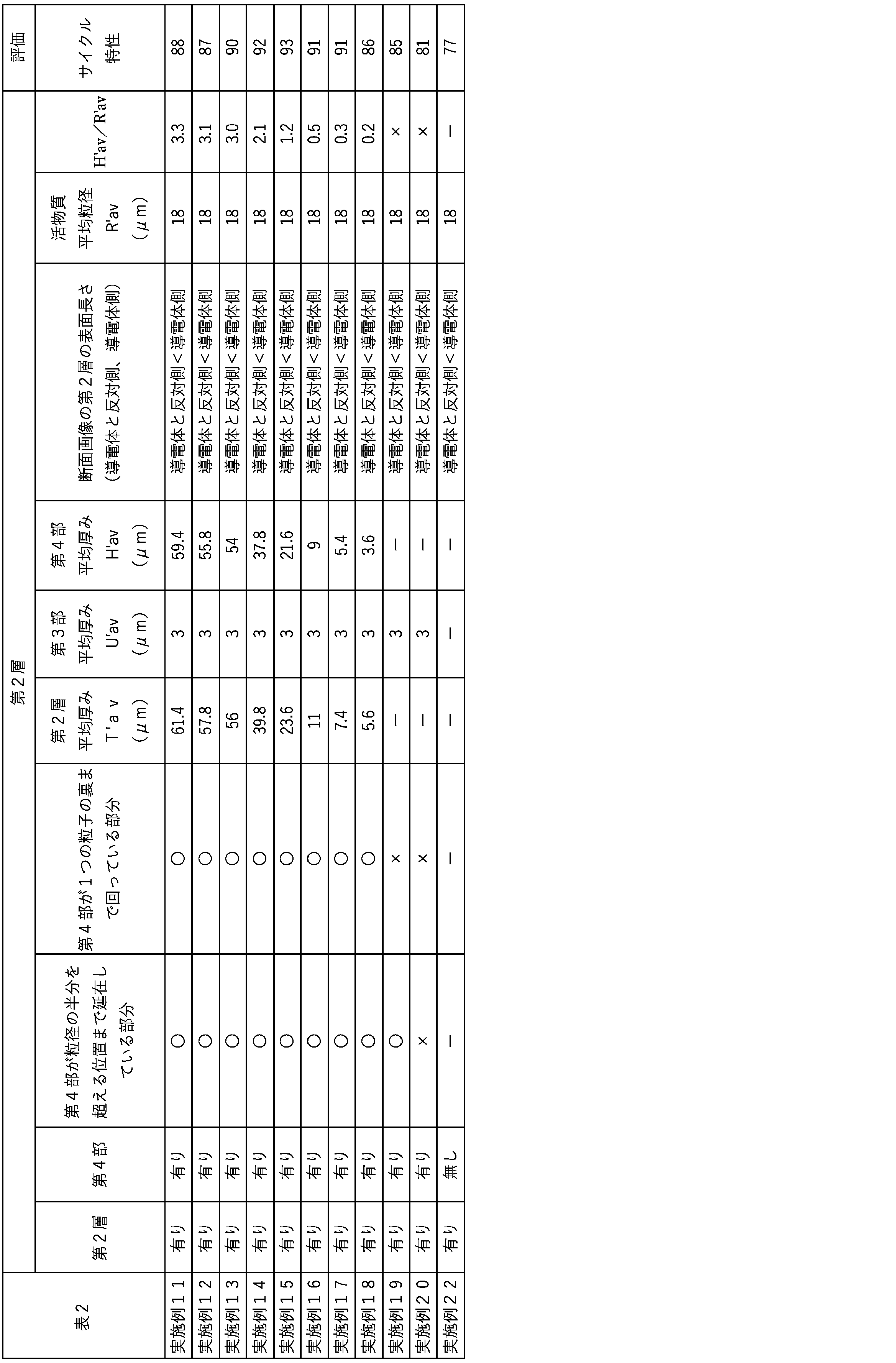

10…負極、12…第1導電体、12a…第1面、12b…第2面、14α…第1活物質層、14β…第2活物質層、14P1(14P)…負極活物質粒子(第1負極活物質粒子)、14P2(14P)…負極活物質粒子(第2負極活物質粒子)、16α…第1層、16αA…第1部、16αB…第2部、16β…第2層、16βA…第3部、16βB…第4部、16αAS,16αBS,16αBS,16βBS…表面、20…セパレータ、30…正極、90…積層体、90C…湾曲部、90M…平坦部、100…蓄電素子、dp…粒径、VV…隙間。
Claims (24)
- 第1面及び前記第1面と反対側を向く第2面を備えた第1導電体と、
前記第1導電体の第1面に設けられ、複数の第1負極活物質粒子を含有する、第1活物質層と、
前記第1活物質層における第1導電体とは反対側において露出する2以上の第1負極活物質粒子に跨がって設けられた第1部、及び、前記第1部から前記第1活物質層の前記第1負極活物質粒子間に侵入している第2部を有し、無機材料を含有する第1層と、を有する負極を備える、蓄電素子。 - 前記第1活物質層と前記第1導電体とが並ぶ第1方向に沿った断面画像において、前記第1層の前記第1導電体側の表面の長さは、前記第1層の前記第1導電体とは反対側の表面の長さよりも大きい、請求項1に記載の蓄電素子。
- 前記第1層の第2部は、前記第1部から、前記第1活物質層と前記第1導電体とが並ぶ第1方向において、前記第1導電体とは反対側において露出する少なくとも1つの前記第1負極活物質粒子の粒径の半分を超える位置まで延在している、請求項1又は2に記載の蓄電素子。
- 前記第1層の第2部は、前記第1部から、前記第1活物質層と前記第1導電体とが並ぶ第1方向において、前記第1導電体とは反対側において露出する少なくとも1つの前記第1負極活物質粒子の最も前記第1導電体に近い部分を覆う位置まで延在している、請求項1又は2に記載の蓄電素子。
- 前記第1活物質層と前記第1導電体とが並ぶ第1方向に沿った断面画像における前記第1層の第2部の平均厚みをHavとし、
前記第1活物質層に含まれる複数の第1負極活物質粒子の平均粒径をRavとした時に、0.3≦Hav/Rav≦3.0を満たす、請求項1又は2に記載の蓄電素子。 - 複数の前記断面画像において、0.3≦Hav/Rav≦3.0を満たす、請求項5に記載の蓄電素子。
- 0.5≦Hav/Rav≦2.0を満たす、請求項5記載の蓄電素子。
- 前記無機材料が無機化合物である、請求項1又は2に記載の蓄電素子。
- 前記無機化合物が酸化アルミニウムを含む、請求項8に記載の蓄電素子。
- 前記第1層は、さらに有機化合物を含む、請求項1又は2に記載の蓄電素子。
- 前記有機化合物がフッ素を含む高分子化合物を含む、請求項10に記載の蓄電素子。
- 前記高分子化合物がポリビニリデンフルオライドである、請求項11に記載の蓄電素子。
- 前記無機材料と前記有機化合物の質量比率が1:1~100:1である、請求項10に記載の蓄電素子。
- 前記第1活物質層の負極活物質粒子が、炭素材料、金属、金属酸化物、半金属、半金属酸化物のうち少なくとも1を含む、請求項1又は2に記載の蓄電素子。
- 前記負極は、
前記第1導電体の第2面に設けられ、複数の第2負極活物質粒子を含有する、第2活物質層と、
前記第2活物質層における第1導電体とは反対側において露出する2以上の前記第2負極活物質粒子に跨がって設けられた第3部、及び、前記第3部から前記第2活物質層の前記第2負極活物質粒子間に侵入している第4部を有し、無機材料を含有する第2層と、をさらに有する、請求項1又は2に記載の蓄電素子。 - 前記第2層の第3部は、前記第3部から、前記第2活物質層と前記第1導電体とが並ぶ第2方向において、前記第1導電体とは反対側において露出する少なくとも1つの前記第2負極活物質粒子の粒径の半分を超える位置まで延在している、請求項15に記載の蓄電素子。
- 前記第2層の第3部は、前記第3部から、前記第2活物質層と前記第1導電体とが並ぶ第2方向において、前記第1導電体とは反対側において露出する少なくとも1つの前記第2負極活物質粒子の最も前記第1導電体に近い部分を覆う位置まで延在している、請求項15に記載の蓄電素子。
- 前記第1層の第1部の前記第1活物質層と前記第1導電体とが並ぶ第1方向における厚みと、前記第2層の第3部の前記第2活物質層と前記第1導電体とが並ぶ第2方向における厚みとは、互いに異なる、請求項15に記載の蓄電素子。
- 前記第1層の第1部の前記第1活物質層と前記第1導電体とが並ぶ第1方向における厚みは、前記第2層の第3部の前記第2活物質層と前記第1導電体とが並ぶ第2方向における厚みよりも大きい、請求項15に記載の蓄電素子。
- さらに、正極と、前記負極と前記正極との間に配置されたセパレータと、を備える、請求項1又は2に記載の蓄電素子。
- さらに、正極と、前記負極と前記正極との間に配置されたセパレータと、を備え、前記負極、前記セパレータ、及び、前記正極を有する積層体が巻回された、請求項15に記載の蓄電素子。
- 前記積層体は、前記第2層が前記第1層よりも内側となるように巻回された、請求項21に記載の蓄電素子。
- 前記第2層の厚みは、前記第1層の厚みよりも小さい、請求項22に記載の蓄電素子。
- 前記積層体は、平坦部と、湾曲部とを交互に有するように巻回され、前記湾曲部の第1層の厚さは、前記平坦部の第1層の厚さよりも薄い、請求項21に記載の蓄電素子。
Priority Applications (4)
| Application Number | Priority Date | Filing Date | Title |
|---|---|---|---|
| PCT/JP2023/024612 WO2025009017A1 (ja) | 2023-07-03 | 2023-07-03 | 蓄電素子 |
| JP2025530816A JPWO2025009017A1 (ja) | 2023-07-03 | 2023-07-03 | |
| CN202380099795.3A CN121399750A (zh) | 2023-07-03 | 2023-07-03 | 蓄电元件 |
| US19/417,436 US20260100426A1 (en) | 2023-07-03 | 2025-12-12 | Power storage element |
Applications Claiming Priority (1)
| Application Number | Priority Date | Filing Date | Title |
|---|---|---|---|
| PCT/JP2023/024612 WO2025009017A1 (ja) | 2023-07-03 | 2023-07-03 | 蓄電素子 |
Related Child Applications (1)
| Application Number | Title | Priority Date | Filing Date |
|---|---|---|---|
| US19/417,436 Continuation US20260100426A1 (en) | 2023-07-03 | 2025-12-12 | Power storage element |
Publications (1)
| Publication Number | Publication Date |
|---|---|
| WO2025009017A1 true WO2025009017A1 (ja) | 2025-01-09 |
Family
ID=94171598
Family Applications (1)
| Application Number | Title | Priority Date | Filing Date |
|---|---|---|---|
| PCT/JP2023/024612 Ceased WO2025009017A1 (ja) | 2023-07-03 | 2023-07-03 | 蓄電素子 |
Country Status (4)
| Country | Link |
|---|---|
| US (1) | US20260100426A1 (ja) |
| JP (1) | JPWO2025009017A1 (ja) |
| CN (1) | CN121399750A (ja) |
| WO (1) | WO2025009017A1 (ja) |
Citations (5)
| Publication number | Priority date | Publication date | Assignee | Title |
|---|---|---|---|---|
| JP2012160292A (ja) * | 2011-01-31 | 2012-08-23 | Sanyo Electric Co Ltd | 非水電解質二次電池 |
| WO2013136426A1 (ja) * | 2012-03-13 | 2013-09-19 | 株式会社日立製作所 | 非水電解質二次電池及びその製造方法 |
| WO2019003770A1 (ja) * | 2017-06-30 | 2019-01-03 | 日立オートモティブシステムズ株式会社 | 二次電池およびその製造方法 |
| JP2019164983A (ja) * | 2018-03-16 | 2019-09-26 | 株式会社リコー | 電極、絶縁層用塗布液、電極の製造方法、非水系蓄電素子及び電子デバイス |
| US20210135236A1 (en) * | 2019-10-31 | 2021-05-06 | EnPower, Inc. | Electrochemical cell with integrated ceramic separator |
-
2023
- 2023-07-03 JP JP2025530816A patent/JPWO2025009017A1/ja active Pending
- 2023-07-03 WO PCT/JP2023/024612 patent/WO2025009017A1/ja not_active Ceased
- 2023-07-03 CN CN202380099795.3A patent/CN121399750A/zh active Pending
-
2025
- 2025-12-12 US US19/417,436 patent/US20260100426A1/en active Pending
Patent Citations (5)
| Publication number | Priority date | Publication date | Assignee | Title |
|---|---|---|---|---|
| JP2012160292A (ja) * | 2011-01-31 | 2012-08-23 | Sanyo Electric Co Ltd | 非水電解質二次電池 |
| WO2013136426A1 (ja) * | 2012-03-13 | 2013-09-19 | 株式会社日立製作所 | 非水電解質二次電池及びその製造方法 |
| WO2019003770A1 (ja) * | 2017-06-30 | 2019-01-03 | 日立オートモティブシステムズ株式会社 | 二次電池およびその製造方法 |
| JP2019164983A (ja) * | 2018-03-16 | 2019-09-26 | 株式会社リコー | 電極、絶縁層用塗布液、電極の製造方法、非水系蓄電素子及び電子デバイス |
| US20210135236A1 (en) * | 2019-10-31 | 2021-05-06 | EnPower, Inc. | Electrochemical cell with integrated ceramic separator |
Also Published As
| Publication number | Publication date |
|---|---|
| JPWO2025009017A1 (ja) | 2025-01-09 |
| CN121399750A (zh) | 2026-01-23 |
| US20260100426A1 (en) | 2026-04-09 |
Similar Documents
| Publication | Publication Date | Title |
|---|---|---|
| JP5223166B2 (ja) | 電池活物質および二次電池 | |
| CN104205465B (zh) | 非水电解质二次电池 | |
| CN105322153B (zh) | 非水电解质电池、电池模块、以及电池组 | |
| CN105934847B (zh) | 电器件 | |
| JP7166265B2 (ja) | 電極、非水電解質電池及び電池パック | |
| JP7247353B2 (ja) | 電極、電池、及び電池パック | |
| CN108140830A (zh) | 锂离子二次电池及其制造方法 | |
| KR101838377B1 (ko) | 비수 전해액 이차 전지 및 그 제조 방법 | |
| JP6607388B2 (ja) | リチウムイオン二次電池用正極及びその製造方法 | |
| CN111758179A (zh) | 正极、电极组及非水电解质电池 | |
| JP7322776B2 (ja) | リチウムイオン二次電池 | |
| CN105934840B (zh) | 电器件 | |
| JP5737595B2 (ja) | 二次電池 | |
| CN115191047A (zh) | 集电体、蓄电元件和蓄电模块 | |
| JP6897228B2 (ja) | 活物質、電極及びリチウムイオン二次電池 | |
| CN105493319B (zh) | 负极活性物质、使用该负极活性物质的负极、以及锂离子二次电池 | |
| JP7003775B2 (ja) | リチウムイオン二次電池 | |
| JP2018174110A (ja) | 集電体、及びリチウムイオン二次電池 | |
| JP5692605B2 (ja) | 非水電解液二次電池 | |
| WO2023166633A1 (ja) | 集電体、蓄電デバイス用電極およびリチウムイオン二次電池 | |
| JP7363443B2 (ja) | リチウムイオン二次電池 | |
| JP6870712B2 (ja) | リチウムイオン二次電池用負極及びリチウムイオン二次電池 | |
| US20200295397A1 (en) | Lithium secondary battery | |
| JP7281402B2 (ja) | 電極および二次電池 | |
| CN105518910B (zh) | 负极活性物质、使用该负极活性物质的负极、以及锂离子二次电池 |
Legal Events
| Date | Code | Title | Description |
|---|---|---|---|
| 121 | Ep: the epo has been informed by wipo that ep was designated in this application |
Ref document number: 23944271 Country of ref document: EP Kind code of ref document: A1 |
|
| ENP | Entry into the national phase |
Ref document number: 2025530816 Country of ref document: JP Kind code of ref document: A |
|
| WWE | Wipo information: entry into national phase |
Ref document number: 2025530816 Country of ref document: JP |
|
| NENP | Non-entry into the national phase |
Ref country code: DE |