WO2025004919A1 - 複合部品 - Google Patents
複合部品 Download PDFInfo
- Publication number
- WO2025004919A1 WO2025004919A1 PCT/JP2024/022172 JP2024022172W WO2025004919A1 WO 2025004919 A1 WO2025004919 A1 WO 2025004919A1 JP 2024022172 W JP2024022172 W JP 2024022172W WO 2025004919 A1 WO2025004919 A1 WO 2025004919A1
- Authority
- WO
- WIPO (PCT)
- Prior art keywords
- layer
- component
- main surface
- composite
- electronic component
- Prior art date
- Legal status (The legal status is an assumption and is not a legal conclusion. Google has not performed a legal analysis and makes no representation as to the accuracy of the status listed.)
- Ceased
Links
Images


Classifications
-
- H—ELECTRICITY
- H10—SEMICONDUCTOR DEVICES; ELECTRIC SOLID-STATE DEVICES NOT OTHERWISE PROVIDED FOR
- H10W—GENERIC PACKAGES, INTERCONNECTIONS, CONNECTORS OR OTHER CONSTRUCTIONAL DETAILS OF DEVICES COVERED BY CLASS H10
- H10W70/00—Package substrates; Interposers; Redistribution layers [RDL]
- H10W70/60—Insulating or insulated package substrates; Interposers; Redistribution layers
- H10W70/62—Insulating or insulated package substrates; Interposers; Redistribution layers characterised by their interconnections
- H10W70/63—Vias, e.g. via plugs
- H10W70/635—Through-vias
-
- H—ELECTRICITY
- H10—SEMICONDUCTOR DEVICES; ELECTRIC SOLID-STATE DEVICES NOT OTHERWISE PROVIDED FOR
- H10W—GENERIC PACKAGES, INTERCONNECTIONS, CONNECTORS OR OTHER CONSTRUCTIONAL DETAILS OF DEVICES COVERED BY CLASS H10
- H10W70/00—Package substrates; Interposers; Redistribution layers [RDL]
- H10W70/60—Insulating or insulated package substrates; Interposers; Redistribution layers
- H10W70/67—Insulating or insulated package substrates; Interposers; Redistribution layers characterised by their insulating layers or insulating parts
- H10W70/69—Insulating materials thereof
- H10W70/698—Semiconductor materials that are electrically insulating, e.g. undoped silicon
-
- H—ELECTRICITY
- H10—SEMICONDUCTOR DEVICES; ELECTRIC SOLID-STATE DEVICES NOT OTHERWISE PROVIDED FOR
- H10W—GENERIC PACKAGES, INTERCONNECTIONS, CONNECTORS OR OTHER CONSTRUCTIONAL DETAILS OF DEVICES COVERED BY CLASS H10
- H10W74/00—Encapsulations, e.g. protective coatings
-
- H—ELECTRICITY
- H10—SEMICONDUCTOR DEVICES; ELECTRIC SOLID-STATE DEVICES NOT OTHERWISE PROVIDED FOR
- H10W—GENERIC PACKAGES, INTERCONNECTIONS, CONNECTORS OR OTHER CONSTRUCTIONAL DETAILS OF DEVICES COVERED BY CLASS H10
- H10W74/00—Encapsulations, e.g. protective coatings
- H10W74/10—Encapsulations, e.g. protective coatings characterised by their shape or disposition
- H10W74/111—Encapsulations, e.g. protective coatings characterised by their shape or disposition the semiconductor body being completely enclosed
-
- H—ELECTRICITY
- H10—SEMICONDUCTOR DEVICES; ELECTRIC SOLID-STATE DEVICES NOT OTHERWISE PROVIDED FOR
- H10W—GENERIC PACKAGES, INTERCONNECTIONS, CONNECTORS OR OTHER CONSTRUCTIONAL DETAILS OF DEVICES COVERED BY CLASS H10
- H10W76/00—Containers; Fillings or auxiliary members therefor; Seals
- H10W76/10—Containers or parts thereof
- H10W76/12—Containers or parts thereof characterised by their shape
-
- H—ELECTRICITY
- H10—SEMICONDUCTOR DEVICES; ELECTRIC SOLID-STATE DEVICES NOT OTHERWISE PROVIDED FOR
- H10W—GENERIC PACKAGES, INTERCONNECTIONS, CONNECTORS OR OTHER CONSTRUCTIONAL DETAILS OF DEVICES COVERED BY CLASS H10
- H10W90/00—Package configurations
Definitions
- This disclosure relates to composite parts.
- FIG. 4F of JP 2019-125779 A Patent Document 1
- This device (400F) includes a redistribution layer (306), a first mold layer (316) arranged on the redistribution layer (306), and a second mold layer (324) arranged on the first mold layer (316).
- the die (318, 320) sealed in the second mold layer (324) is connected to the bridge die (310) sealed in the first mold layer (316) via an electrical connection part (312), and is connected to the redistribution layer (306) via an electrical connection part (314).
- the objective of this disclosure is to provide composite parts with superior reliability.
- the inventors conducted extensive research to solve the above problems and discovered that cracks occur because the strength of the entire device is insufficient and because the exposed areas of the first and second molded layers, which have relatively high hygroscopicity, are large. Based on this technical knowledge, the inventors came up with the present disclosure, which provides side walls at both ends to increase the strength of the entire device and reduce exposure at both ends of the first and second molded layers. In other words, the present disclosure includes the following embodiments.
- a composite part comprises: A composite component incorporating one or more electronic components, a Si-based layer having a first main surface and a second main surface opposite to the first main surface; a redistribution layer disposed on the first main surface; a through-Si via electrically connected to the redistribution layer and penetrating the Si base layer; an electronic component electrically connected to the through-Si via and disposed on the second main surface; a sidewall portion disposed to surround the electronic component and form a recess with the Si base layer; and a resin sealing portion that seals the electronic component.
- the composite component has a sidewall portion that surrounds the electronic component and is arranged to form a recess with the Si base layer. This improves the strength of the entire composite component. Furthermore, because the sidewall portions are arranged at both ends of the composite component in a cross-sectional view, the resin sealing portion is no longer exposed at both end faces of the composite component, and the exposed area of the resin sealing portion is reduced. This prevents moisture from penetrating from the outside into the composite component. As a result, the composite component according to this embodiment has superior reliability.
- Composite parts according to one embodiment of the present disclosure have superior reliability.
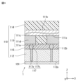
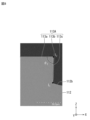
- FIG. 1 is a plan view illustrating a composite part according to a first embodiment.
- FIG. 2 is a cross-sectional view taken along line II of FIG.
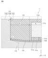
- FIG. 3 is an enlarged view of part A in FIG. 2 .
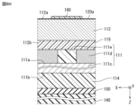
- FIG. 3 is an enlarged view of part B in FIG. 2 .
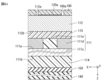
- FIG. 2 is a cross-sectional view showing a cavity in the composite part according to the first embodiment.
- 5A to 5C are explanatory diagrams illustrating a manufacturing method of the composite part according to the first embodiment.
- 5A to 5C are explanatory diagrams illustrating a manufacturing method of the composite part according to the first embodiment.
- 5A to 5C are explanatory diagrams illustrating a manufacturing method of the composite part according to the first embodiment.
- 5A to 5C are explanatory diagrams illustrating a manufacturing method of the composite part according to the first embodiment.
- 5A to 5C are explanatory diagrams illustrating a manufacturing method of the composite part according to the first embodiment.
- 5A to 5C are explanatory diagrams illustrating a manufacturing method of the composite part according to the first embodiment.
- 5A to 5C are explanatory diagrams illustrating a manufacturing method of the composite part according to the first embodiment.
- 5A to 5C are explanatory diagrams illustrating a manufacturing method of the composite part according to the first embodiment.
- 5A to 5C are explanatory diagrams illustrating a manufacturing method of the composite part according to the first embodiment.
- 5A to 5C are explanatory diagrams illustrating a manufacturing method of the composite part according to the first embodiment.
- 5A to 5C are explanatory diagrams illustrating a manufacturing method of the composite part according to the first embodiment.
- 5A to 5C are explanatory diagrams illustrating a manufacturing method of the composite part according to the first embodiment.
- 5A to 5C are explanatory diagrams illustrating a manufacturing method of the composite part according to the first embodiment.
- 5A to 5C are explanatory diagrams illustrating a manufacturing method of the composite part according to the first embodiment.
- 5A to 5C are explanatory diagrams illustrating a manufacturing method of the composite part according to the first embodiment.
- FIG. 11 is a cross-sectional view illustrating a composite part according to a second embodiment.
- FIG. 11 is a cross-sectional view showing a cavity in a composite part according to a second embodiment.
- 5A to 5C are explanatory diagrams illustrating a manufacturing method of the composite part according to the first embodiment.
- 5A to 5C are explanatory diagrams illustrating a manufacturing method of the composite part according to the first embodiment.
- the term "above” is used immediately after the name of a component to indicate the location of the component, and does not simply mean the vertically upper side of the component, but means that the component is placed in contact with the component.
- the vertical direction is parallel to the Z direction
- the reverse Z direction is the vertically downward direction
- the forward Z direction is the vertically upward direction.
- the redistribution layer 120 is placed on the first main surface 112a (of the Si-based layer 112) means that the redistribution layer 120 is placed so as to be in contact with the first main surface 112a (the lower surface).
- the electronic component 111 is placed on the second main surface 112b (of the Si-based layer 112) means that the electronic component 111 is placed so as to be in contact with the second main surface 112b (the upper surface).
- composite part The composite component according to the first embodiment has one or more electronic components built in.
- a composite component having two built-in electronic components will be described as an example.
- the composite part according to the first embodiment has: A composite component incorporating two electronic components, a Si-based layer having a first main surface and a second main surface opposite to the first main surface; a redistribution layer disposed on the first major surface; a through-Si via electrically connecting to the redistribution layer and penetrating the Si base layer; an electronic component disposed on the second main surface and electrically connected to the through-Si via; a sidewall portion disposed to surround an electronic component and form a recess with the Si base layer; and a resin sealing portion that seals the electronic component.
- the composite part according to the first embodiment has superior reliability, the reason for which is presumed to be as follows.
- the composite component according to the first embodiment includes a sidewall portion that surrounds the electronic component and is arranged to form a recess together with the Si base layer. This improves the strength of the entire composite component.
- the sidewall portion is arranged at both ends of the composite component in a cross-sectional view, the resin encapsulation portion is not exposed at both end faces of the composite component, and the exposed area of the resin encapsulation portion is reduced. This suppresses the intrusion of moisture from the outside into the composite component. As a result, the composite component according to this embodiment has better reliability.
- the composite parts are cut at the sidewalls located at both ends to separate them. Therefore, compared to cutting at the resin sealing parts, the cut surfaces formed are less likely to have irregularities due to, for example, falling off of filler, improving the manufacturing efficiency of composite parts.
- Figure 1 is a plan view that shows a schematic diagram of the composite part according to the first embodiment of the present disclosure.
- Figure 2 is a cross-sectional view taken along line II in Figure 1.
- Figure 3 is an enlarged view of part A in Figure 2.
- Figure 4 is an enlarged view of part B in Figure 2.
- the composite component 1 As shown in Figures 1 and 2, the composite component 1 according to the first embodiment has a generally rectangular parallelepiped shape with adjacent faces connected generally perpendicularly.
- the composite component 1 incorporates two electronic components 111.
- the direction parallel to the thickness of the composite component 1 is the Z direction, with the forward Z direction being the upper side and the reverse Z direction being the lower side.
- the direction perpendicular to the Z direction in the cross section of the composite component 1 shown in Figure 2 is the X direction.
- the direction perpendicular to the cross section of the composite component 1 shown in Figure 2 is the Y direction.
- the composite component 1 includes an electronic component layer 110 and a redistribution layer 120 that is bonded to the underside of the electronic component layer 110.
- the electronic component layer 110 has a lower surface that is bonded (joined) to the rewiring layer 120.
- the electronic component layer 110 has two electronic components 111, a Si base layer 112, a sidewall portion 113, a resin sealing portion 114, an adhesive layer 115, and a Si through via 117.
- the electronic components 111 are arranged in the electronic component layer 110.
- the electronic components 111 are arranged on the second main surface 112b of the Si base layer 112.
- the electronic component 111 has an electronic component body 111c having a first surface 111a and a second surface 111b facing each other, a plurality of component electrodes 111d arranged on the first surface 111a, and an insulating portion 111e arranged between the plurality of component electrodes 111d.
- the electronic component 111 is supported on the Si base layer 112 via an adhesive layer 115.
- the electronic component 111 is sealed by a resin sealing portion 114 in the electronic component layer 110.
- the component electrodes 111d of the electronic component 111 are electrically connected to the rewiring layer 120 via a Si through via 117.
- the electronic components 111 may be of the same type or different types.
- the two electronic components 111 are both arranged in the electronic component layer 110 such that their first surfaces 111a are positioned on the rewiring layer 120 side relative to their second surfaces 111b. These two electronic components 111 are both arranged in the same direction and connected to the rewiring layer 120. In this way, the composite component 1 has simple wiring, which makes it possible to manufacture the composite component with excellent efficiency.
- the electronic component 111 is, for example, an electronic component in which one or more elements are integrated in a material similar to the material that constitutes the Si-based layer 112.
- the electronic component 111 is, for example, an active component (more specifically, a CPU, a GPU, an LSI, etc.) and a passive component (more specifically, a capacitor, a resistor, an inductor, etc.).
- the electronic component body 111c includes, for example, a ceramic or semiconductor material (more specifically, silicon, etc.).
- the component electrode 111d is electrically connected to the redistribution layer 120 only through the through-Si via 117.
- the via wiring electrically connecting the component electrode 111d to the redistribution layer 120 is composed only of the through-Si via 117, and therefore does not have (does not require) a bump (e.g., a solder bump). Therefore, the composite component 1 according to this embodiment can further reduce the parasitic impedance caused by the via wiring. This also improves the electronic characteristics of electronic devices that use the composite component 1. Furthermore, because the wiring length can be shorter than before, the thickness of the composite component 1 can be reduced, making it possible to make the composite component 1 smaller, thinner, and lower-profile.
- the component electrode 111d is made of a conductive material such as Cu, Ni, Sn, and Al, or an alloy containing these. Of these, the conductive material is preferably the same material as the Si through via 117.
- the thickness of the component electrode 111d is, for example, 1 ⁇ m to 30 ⁇ m, and preferably 5 ⁇ m or less.
- the component electrode 111d can be thinned to a thickness of 1 to 5 ⁇ m.
- the thickness of the component electrode 111d can be, for example, 1/4 to 1/6 times the thickness of the electronic component body 111c.
- the insulating portion 111e functions as a layer that electrically insulates the component electrodes 111d.
- the thickness of the insulating portion 111e is, for example, 1 to 30 ⁇ m, and preferably 5 ⁇ m or less.
- the component electrode 111d can be thinned to a thickness of 1 to 5 ⁇ m.
- the thickness of the insulating portion 111e can be, for example, 1/4 to 1/6 times the thickness of the electronic component body portion 111c.
- the thickness of the insulating portion 111e may be the same as that of the component electrode 111d, in which case the bottom surface of the insulating portion 111e and the bottom surface of the component electrode 111d are flush with each other. When the bottom surface of the insulating portion 111e and the bottom surface of the component electrode 111d are flush with each other, the thickness of the adhesive layer 115 can be reduced, thereby making it possible to reduce the size and height of the composite component 1.
- the Si base layer 112 has a first main surface 112a and a second main surface 112b opposite to the first main surface 112a.
- the Si base layer 112 supports two electronic components 111 via an adhesive layer 115 on the second main surface 112b, and is connected to the redistribution layer 120 on the first main surface 112a.
- the Si base layer 112 is substantially composed of Si.
- the thickness of the Si base layer 112 is, for example, 150 ⁇ m or less, preferably 50 ⁇ m or less, and more preferably 30 ⁇ m or less.
- the reason why the thickness of the Si base layer 112 can be made extremely thin in this way is that in the manufacturing method of the composite component 1 described later, the Si support 140 is bonded to the Si base layer 112 to reinforce its strength, so that even if the Si base layer 112 is ground to be thin, damage (such as cracks) of the Si base layer 112 due to insufficient strength is unlikely to occur (see FIG. 6F).
- the reinforcement of strength by the Si support 140 makes it possible to manufacture the composite component 1.
- the thickness of the Si base layer 112 can be made extremely thin compared to the conventional method, the length of the via wiring (i.e., the Si through via 117) that electrically connects the component electrodes 111d of the two electronic components 111 to the rewiring layer 120 can be shortened. This reduces the parasitic impedance due to the via wiring, and improves the electrical characteristics of the electronic device using the composite component 1.
- the second main surface 112b of the Si base layer 112 mounts the electronic component 111.
- the region (mounting region) on the second main surface 112b where the electronic component 111 can be mounted is a flat region R2 of the second main surface 112b in the cross-sectional view shown in FIG. 4.
- the region (difficult-to-mount region) on the second main surface 112b where the electronic component 111 is difficult to mount is a curved region R1 of the second main surface 112b in the cross-sectional view shown in FIG. 4.
- the curved region R1 is a region from the inner surface 113c of the side wall portion 113 to the flat second main surface 112.
- the length of the curved region R1 is preferably 100 ⁇ m or less, more preferably 80 ⁇ m or less, even more preferably 60 ⁇ m or less, and particularly preferably 50 ⁇ m or less.
- the sidewall portion 113 is disposed on the second main surface 112b of the Si base layer 112 so as to surround the two electronic components 111.
- the sidewall portion 113 is disposed at both ends of the electronic component layer 110 so as to surround the entire two electronic components 111.
- the sidewall portion 113 is integrated with the Si base layer 112 in a cross-sectional view. Being integrated further improves the strength of the entire composite component 1.
- the thickness of the sidewall portion 113 is, for example, 90 to 130 ⁇ m.
- the sidewall portion 113 is, for example, substantially composed of Si.
- the inner surface 113c of the side wall portion 113 and the second main surface 112b of the Si-base layer 112 form an obtuse angle (more specifically, an angle greater than 90°).
- internal stress which may occur during the manufacture of the composite component 1 and during operation of the composite component 1 is less likely to concentrate, making the composite component 1 less likely to crack. This further improves the reliability of the composite component 1.
- the angle ⁇ 1 between the inner side surface 113c and the second main surface 112b refers to an angle formed at a bending point (connection point, joint) I1 between the substantially straight inner side surface 113c and the second main surface 112b in a ZX cross section at a magnification of 700 times (an SEM image taken at a magnification of 700 times using a scanning electron microscope ("FlexSEM” manufactured by Hitachi High-Technologies Corporation)), and in the case where the second main surface 112b is a curved surface, the angle ⁇ 1 refers to an angle formed at the bending point I1 between the substantially straight inner side surface 113c and a tangent T that contacts the bending point I1 at which the inner side surface 113c and the second main surface 112b are connected.
- the ZX cross section of the composite part 1 for determining the obtuse angle is formed by cutting the composite part 1, which has a substantially rectangular shape in a plan view as shown in FIG. 1, along a plane (II cross section in FIG. 1) that includes point O where the diagonal lines (dashed lines in FIG. 1) intersect and is parallel to the side surface of the composite part 1.
- the angle ⁇ 1 between the inner surface 113c and the second main surface 112b is preferably 100° or more, more preferably 120° or more, and even more preferably 130° or more, from the viewpoint of suppressing local concentration of internal stress and suppressing the occurrence of cracks in the composite component 1.
- the angle ⁇ 1 between the inner surface 113c and the second main surface 112b can be achieved by non-uniformly supplying an etching gas to an object to be etched, as will be described in detail later in the manufacturing method of a composite part.
- the angle ⁇ 1 between the inner surface 113c and the second main surface 112b is preferably 130° or less, more preferably 120° or less, and even more preferably 100° or less, from the viewpoint of increasing the area that can be mounted on the second main surface 112b of the electronic component 111.
- the ratio of the width between the opposing inner surfaces 113c of the recess to the width of the sidewall 113 is 10 to 1000. If the width ratio is 10 or more, the proportion of the sidewall 113 is above a certain level, and the rigidity of the composite component 1 is high. On the other hand, if the width ratio is 1000 or less, the area (mounting area) in which the electronic component 111 can be mounted is above a certain level, allowing for further integration.
- the width of the side wall 113 is the length between the inner surface 113c and the outer surface of the side wall 113, on a straight line (dash-dotted line in FIG. 1) that includes the point O where the diagonal line (dashed line in FIG. 1) intersects in the plan view shown in FIG. 1 and is parallel to the side surface of the composite part 1.
- the width between opposing inner surfaces 113c of the recess is the length between one inner surface 113c and the inner surface 113c facing the other inner surface 113c, on a straight line (dash-dotted line in FIG. 1) that includes the point O where the diagonal line (dashed line in FIG. 1) intersects in the plan view shown in FIG. 1 and is parallel to the side surface of the composite part 1.
- the resin sealing portion 114 seals the two electronic components 111 .
- the resin sealing portion 114 includes, for example, a resin (more specifically, an epoxy resin or the like) and a filler (more specifically, a silica filler or the like), and the two electronic components 111 can be integrated with the resin. Since the two electronic components 111 can be integrated with the resin, even if the two electronic components 111 have different dimensions and shapes, the two electronic components 111 can be disposed in the electronic component layer 110. This allows for a high degree of design freedom, and two or more electronic components 111 can be combined according to the application. For example, the composite component 1 can incorporate different types of electronic components 111.
- the adhesive layer 115 bonds the two electronic components 111 to the second main surface 112b of the Si base layer 112.
- the thickness of the adhesive layer 115 refers to the thickness in the Z direction from the lower surface of the component electrode 111d to the second main surface 112b of the Si base layer 112.
- the thickness of the adhesive layer 115 is, for example, 4 to 6 ⁇ m.
- the through-Si via 117 penetrates the Si base layer 112 (and the adhesive layer 115 ) to electrically connect the component electrode 111 d and the redistribution layer 120 .
- the through-Si via 117 has a through-Si via body 117a and an extending portion 117b.
- the through-Si via body 117a is electrically connected to the rewiring layer 120 and penetrates the Si base layer 112.
- the extending portion 117b is electrically connected to the through-Si via body 117a, extends from the second main surface 112b of the Si base layer 112, penetrates the adhesive layer 115, and electrically connects to the component electrode 111d.
- the via wiring electrically connecting the component electrode 111d to the rewiring layer 120 is composed only of the through-Si via 117, so that it does not have (does not require) a bump (e.g., a solder bump). Therefore, the composite component 1 according to this embodiment can further reduce the parasitic impedance caused by the via wiring. This also improves the electronic characteristics of the electronic device using the composite component 1. Furthermore, since the wiring length can be shortened compared to the conventional case, the thickness of the composite component 1 can be reduced, and the composite component 1 can be made smaller, thinner, and lower in height.
- the length of the via wiring (i.e., the length of the through Si via 117 in the stacking direction) is, for example, 3 ⁇ m to 36 ⁇ m.
- the (XY) cross-sectional shape of the through Si via 117 is substantially circular
- the (XY) cross-sectional diameter (diameter) is, for example, 1 to 20 ⁇ m.
- the through Si via 117 is substantially linear in the stacking direction in Fig. 2.
- the cross-sectional shape of the through Si via 117 in the ZX plane is substantially rectangular in Fig. 2.
- the (XY) cross-sectional shape of the through Si via 117 in the XY plane is, for example, substantially circular, substantially polygonal, or substantially polygonal with rounded corners.
- a seed layer and a barrier layer may be provided between the through-Si via 117 and the resin sealing portion 114 and between the through-Si via 117 and the adhesive layer 115 .
- the redistribution layer 120 is disposed on the first main surface 112a of the Si base layer 112.
- the redistribution layer 120 is a multi-layer wiring layer (sheet or substrate).
- the redistribution layer 120 has wiring (conductive wiring) 120b and a dielectric film 120a substantially composed of an inorganic material (inorganic insulating material). Note that the dielectric film 120a and wiring 120b are not shown in the redistribution layer 120 in FIG. 3, but the redistribution layer 120 is composed of a plurality of dielectric films 120a and wiring 120b stacked together. For example, a plurality of dielectric films 120a and wiring 120b in FIG. 6L described later are stacked together to form the redistribution layer 120 in FIG. 6M described later.
- the wiring 120b has a conductive via.
- the conductive via electrically connects the wiring between different layers in the redistribution layer 120.
- the wiring 120b includes a conductive material.
- the conductive material is, for example, Cu, Ag, and Au, and alloys containing these, among which Cu is preferable.
- the redistribution layer 120 can have multiple layers, for example, two or more layers of wiring 120b and one or more layers of dielectric film 120a.
- the thickness of the redistribution layer 120 is a value (unit: ⁇ m) obtained by multiplying the thickness of one layer of the wiring 120b and the dielectric film 120a that constitute the redistribution layer 120 by the total number of layers in the redistribution layer 120. Note that the thickness of one layer of the wiring 120b mentioned here does not include the thickness of the conductive via.
- the dielectric film 120a is made of an inorganic insulating material as an insulating material.
- inorganic insulating materials include silicon oxide ( SiO2 ), silicon nitride (SiN, Si3N4 ), and silicon carbonitride (SiCN).
- SiO2 silicon oxide
- SiN silicon nitride
- SiCN silicon carbonitride
- the wiring width can be reduced to about 1/10 compared to a dielectric film made of an organic insulating material. This allows the composite component 1 to be further miniaturized and thinned.
- the dielectric film 120a may be a multi-component film containing two or more components.
- the multi-component film may be a multi-layer film in which multiple layers are formed for each component.
- the manufacturing method of the composite part 1 may be, for example, a cavity forming step of forming a recessed cavity having a Si base layer and a lattice-shaped sidewall portion disposed on the Si base layer; an electronic component bonding step of bonding one or more electronic components to a bottom surface of the cavity; an electronic component sealing step of sealing one or more electronic components with resin to form a resin sealed portion; a Si-based layer thinning step of thinning the Si-based layer; a through-hole forming step of forming a through-hole in the thinned Si base layer to expose a portion of the electronic component;
- the method includes a through-Si via forming step of forming a through-Si via in the through hole, and a rewiring layer forming step of forming a rewiring layer.
- the manufacturing method of the composite component 1 further includes: an insulating portion forming step of forming an insulating portion between component electrodes of the electronic component; a resin sealing portion thinning step of thinning the resin sealing portion; a Si support bonding step of bonding a Si support to the resin sealing layer; a dielectric film forming step of forming a dielectric film having a predetermined pattern on a Si-based layer; an operation confirmation process for confirming the operation of the composite part; and a dicing step of dividing the substrate into individual pieces by dicing.
- FIGS. 9A to 9B and 6A to 6N are views for explaining the method for manufacturing the composite component 1.
- the method for manufacturing the composite component 1 according to the first embodiment includes an insulating portion forming step, a cavity forming step, an electronic component bonding step, an electronic component sealing step, a resin sealing portion thinning step, a Si support bonding step, a Si base layer thinning step, a dielectric film forming step, a through hole forming step, a Si through via forming step, a rewiring layer forming step, an operation checking step, and a dicing step.
- a mother assembly in which composite components 1 are assembled is produced from the cavity forming step to the operation checking step.
- insulating portions 111e are formed between the component electrodes 111d of the electronic component 111. Specifically, in the insulating portion forming process, a coating film containing a resin is formed, and a planarization process is performed to form the insulating portions 111e. A solution containing a resin and a solvent is applied using a spin coating method to form the coating film. Here, the lowest part of the coating film is made higher than the highest part of the component electrodes 111d. In other words, the coating film is formed so that all of the multiple component electrodes 111d are completely buried in the coating film. As shown in FIG. 9A, the coating layer is dried to form the insulating portions 111e. The insulating portions 111e before the subsequent planarization process preferably completely cover the component electrodes 111d.
- a surface planer, a chemical mechanical polisher (CMP) and a grinder are used to grind and planarize the surfaces of the component electrodes 111d and the insulating portions 111e, and the insulating portions 111e are formed between the component electrodes 111d.
- CMP chemical mechanical polisher
- a grinder is used to grind and planarize the surfaces of the component electrodes 111d and the insulating portions 111e, and the insulating portions 111e are formed between the component electrodes 111d.
- a recessed cavity having a Si base layer 112 and a lattice-shaped sidewall portion 113 arranged on the Si base layer 112 is formed.
- a Si wafer is first prepared.
- a mask covering the portion corresponding to the sidewall portion 113 in a plan view is formed on the main surface of the Si wafer.
- dry etching more specifically, reactive ion etching (RIE) and sputter etching, etc.
- a recessed cavity is formed having the Si base layer 112, a substantially rectangular bottom surface (in a plan view) arranged on the Si base layer 112, and the sidewall portion 113 arranged in a lattice shape so as to surround the substantially rectangular bottom surface.
- the recessed cavity is formed by removing a part of it by etching, so that the sidewall portion 113 and the Si base layer 112 are integrated.
- the depth of the cavity (the length in the Z direction from the upper surface of the resin sealing portion 114 , which is flush with the sidewall portion 113 , to the second main surface 112 b of the Si base layer 112 ) is, for example, 200 ⁇ m, which is greater than or equal to the thickness of the electronic component 111 .
- the mode in which the inner surface 113c of the sidewall portion 113 and the second main surface 112b (bottom surface) of the Si base layer 112 form an obtuse angle at the bending point I1 can be realized by adopting a dry etching method and supplying an etching gas non-uniformly to the etching target (Si wafer).
- the non-uniform supply of the etching gas means that the amount of the etching gas supplied to the vicinity of the boundary between the mask and the opening of the mask is made smaller than the amount of the etching gas supplied to the opening other than the vicinity of the boundary.
- Such non-uniform supply of the etching gas can be controlled, for example, by making the pressure of the etching gas higher than the pressure of the etching gas in normal use.
- the shape of the Si wafer may be, but is not limited to, a flat cylindrical shape when viewed from above in a plan view.
- the thickness of the Si wafer is, for example, 775 ⁇ m (Si wafer diameter ⁇ 300 mm), 725 ⁇ m ( ⁇ 200 mm), 675 ⁇ m ( ⁇ 150 mm), and 525 ⁇ m ( ⁇ 100 mm).
- the cavity formation process may be performed before the insulating section formation process.
- Both the Si base layer 112 and the side wall section 113 are substantially composed of Si. Note that "flat” refers to a cylindrical shape in which the ratio of the height to the diameter of the circle (aspect ratio) is small.
- FIG. 5 is a cross-sectional view showing a cavity (where the sidewall portion 113 and the Si base layer 112 are integrated) formed in the cavity forming step of the manufacturing method of the composite part 1.
- FIG. 5 is a scanning electron microscope image of the cut surface of the cavity (SEM image taken at a magnification of 700 times using a scanning electron microscope (FlexSEM manufactured by Hitachi High-Tech Corporation). This cut surface was formed by cutting along a plane that includes the intersection point of the diagonal lines of the approximately rectangular bottom surface of the cavity in a plan view and is parallel to the surface to be cut in the dicing step. As shown in FIG.
- the angle ⁇ 1 between the inner surface 113c of the sidewall portion 113 and the tangent T of the second main surface 112b at the bending point I 1 between the inner surface 113c and the second main surface 112b of the Si base layer 112 was an obtuse angle.
- the angle formed at bending point I2 between inner surface 113c of side wall 113 and upper surface 113a of side wall 113 was 90°.
- the difficult-to-mount region R1 on second main surface 112b was a region extending from side wall 113 to about 77 ⁇ m. In the cavity shown in FIG.
- side wall 113 had a width of 100 ⁇ m, the width between opposing inner surfaces 113c of the recess was 2000 ⁇ m, and the ratio of the width between opposing inner surfaces 113c of the recess to the width of side wall 113 was 20.
- one or more electronic components 111 are bonded to the bottom surface of the cavity (the second main surface 112b of the Si base layer 112). More specifically, first, An adhesive layer 115 (strictly speaking, a coating film of an adhesive) is formed. The coating film of the adhesive is formed on the second main surface 112b of the Si base layer 112. The coating film is formed by, for example, spin coating. In the case of forming a coating film using a die attach film, strictly speaking, the die attach film is formed on the part electrode 111d side of the electronic component 111. The film is attached in advance, and the electronic component 111 in this state is placed on the second main surface 112b of the Si base layer 112.
- the adhesive is, for example, a thermosetting resin.
- the thermosetting resin is, for example, a thermosetting resin containing a repeating unit derived from benzocyclobutene (BCB), such as 1,3-divinyl-1,1,3,3-tetramethyldisiloxane-bis-benzocyclobutene. It can be obtained by polymerizing (DVS-bis-BCB).
- BCB benzocyclobutene
- DVD 1,3-divinyl-1,1,3,3-tetramethyldisiloxane-bis-benzocyclobutene. It can be obtained by polymerizing (DVS-bis-BCB).
- Commercially available products include "CYCLOTENE" manufactured by Dow Chemical.
- one or more electronic components 111 are placed (mounted) in the air and face-down on the bottom surface of the cavity (the second main surface 112b of the Si base layer 112) using a device such as a flip-chip holder and mounter so that the component electrodes 111d and insulating portions 111e are in contact with the bottom surface of the cavity (the second main surface 112b of the Si base layer 112) via the adhesive layer 115 (strictly speaking, a coating of adhesive).
- the adhesive coating is cured to form the adhesive layer 115.
- the adhesive coating is cured by heating in an oven.
- the oven may further include a pressure adjustment section (more specifically, a member having a pressure reducing function and a pressure applying function).
- a pressure adjustment section more specifically, a member having a pressure reducing function and a pressure applying function.
- one or more electronic components 111 are sealed with resin to form a resin sealing portion 114.
- a liquid resin is applied to the cavity in which one or more electronic components 111 are mounted, so as to fill the recess and the side wall portion 113, using a dispenser.
- the applied liquid resin is molded using a compression molding device.
- the liquid resin is hardened, for example, using a hot air circulation oven. This forms the resin sealing portion 114.
- a tablet-like resin or a powdered resin may be used instead of the liquid resin.
- the resin sealing portion 114 is thinned. Specifically, in the resin sealing portion thinning process, as shown in FIG. 6D, a Si wafer back grinder is used to thin the sidewall portion Resin sealing portion 114 is ground to be thinned so as to expose the upper surface of 113. In the electronic component thinning step, the surface of resin sealing portion 114 on the second surface 111b side of electronic component 111 is ground. It is preferable to grind away as much as possible.
- the resin encapsulation 114 of the electronic component layer 110 is ground, but one or more electronic components 111 may also be ground. However, care must be taken not to damage the internal functional parts of the electronic components 111.
- the functional parts are, for example, the dielectric and electrodes in the case of a capacitor, and the wiring in the case of an inductor.
- a back grinder may be used, followed by planarization by CMP.
- CMP the object is fixed to the Si support 140 and rotated on a polishing pad while a slurry containing chemical substances and abrasive grains is supplied. Chemical polishing with chemicals and mechanical polishing with a grindstone are performed simultaneously to planarize the object.
- Si support bonding process In the Si support lamination process, as shown in FIG. 6E, the Si support 140 is laminated to the resin sealing portion 114. Specifically, the Si wafer described in the cavity formation process is separately prepared as the Si support 140. Next, the adhesive layer 150 (strictly speaking, a coating film of adhesive) is formed on the Si support 140 by the method described in the electronic component bonding process. Thereafter, the resin sealing portion 114 is laminated on the Si support 140 so that the ground surface of the resin sealing portion 114 contacts the coating film, and pressure is applied and heated. As a result, the coating film of the adhesive is hardened to form the adhesive layer 150, and the Si support 140 is placed on the ground surface of the resin sealing portion 114 via the adhesive layer 150.
- the purpose of providing the Si support 140 is to prevent the occurrence of adverse effects (more specifically, a decrease in strength, etc.) due to the layer in the manufacturing process being thinner than the conventional one in the subsequent Si base layer thinning process.
- the Si support 140 can be thinned before lamination in order to improve processability. This is because a dielectric film is formed using a semiconductor device device in a subsequent process.
- a Si wafer ⁇ 300 mm, typical thickness 775 ⁇ m
- the adhesive strength of the adhesive layer 150 can be weakened in advance by irradiation with ultraviolet light (UV light), heating, or etching with a chemical solution, in anticipation of its subsequent removal.
- the Si base layer 112 is thinned. Specifically, in the Si base layer thinning step, as shown in FIG. 6F, the Si base layer 112 is ground in the same manner as in the resin sealing portion thinning step, to thin the Si base layer 112 and flatten the ground surface. In the Si base layer thinning step, the Si base layer 112 is thinned while being (indirectly) supported by the Si support 140, so that the Si base layer 112 can be effectively thinned. As a result, the manufacturing method of the composite component 1 according to the present embodiment can manufacture a composite component 1 that is excellent in electronic component modules and has a low height and a small size.
- the amount of grinding is as large as possible while preventing the above-mentioned adverse effects and, for example, maintaining a certain strength.
- the thickness of the Si base layer 112 after thinning is preferably 3 ⁇ m or more.
- a dielectric film 120a having a predetermined pattern is formed on the Si base layer 112, as shown in FIGS. 6G, 6H and 6I.
- Figures 6G to 6I are enlarged views of a portion corresponding to part C in Figure 6F.
- Figures 6J to 6M are mainly views relating to the formation of through-Si via 117 and redistribution layer 120, it should be noted that for convenience, through-Si via 117, redistribution layer 120, and the areas where they are formed are enlarged so as to occupy a large area.
- a dielectric film (thickness 0.1 to 0.2 ⁇ m) 120a is formed on the entire surface of the Si base layer 112 using a chemical vapor deposition (CVD) method such as PECVD, as shown in FIG. 6G.
- the dielectric film 120a may be formed in one or more layers.
- the thicknesses of the layers may be, in order from the Si base layer 112 side, SiO 2 : 0.25 ⁇ m/Si 3 N 4 : 0.1 ⁇ m/SiO 2 : 0.25 ⁇ m/Si 3 N 4 0.1 ⁇ m.
- the dielectric film forming step can clean the surface of the Si base layer 112 before forming the dielectric film 120a.
- the cleaning can be, for example, wet cleaning and oxygen plasma ashing.
- the dielectric film 120a is patterned using a photolithography method.
- a liquid resist is spin-coated to form a photoresist film 160 on the entire surface of the dielectric film 120a.
- the photoresist film 160 is exposed through a mask corresponding to a predetermined pattern.
- the exposed photoresist film 160 is developed.
- the dielectric film 120a of the photoresist film 160 is selectively removed using RIE (Reactive Ion Etching). For example, when the above-mentioned four-layer dielectric film 120a is formed, two layers on the front side of the dielectric film 120a (the surface side of the dielectric film 120a facing the Si base layer 112) are selectively removed.
- RIE Reactive Ion Etching
- the dielectric film 120a having a predetermined pattern is formed on the Si base layer 112.
- the dielectric film 120a also functions as an insulating film that electrically insulates between two Si through vias 117 shown in FIG. 6L described later.
- the first main surface 112a of the Si base layer 112 may further have a mark layer. The mark layer can be detected by an IR camera to perform alignment in a photolithography method.
- through holes 112c, 115c are formed in the thinned Si base layer 112 and adhesive layer 115 to expose a part of the surface of the component electrode 111d.
- a photoresist film 160 is formed on the entire surface.
- the photoresist film 160 is exposed through a mask corresponding to the pattern of the Si through via 117.
- the exposed photoresist film 160 is developed to form a photoresist film 160 having a predetermined pattern as shown in FIG. 6J.
- FIG. 6K the Si base layer 112 and adhesive layer 115 present in the Z direction from the opening 160a of the photoresist film 160 are selectively removed (etched).
- the etching is performed using, for example, RIE and laser irradiation.
- the through holes 112c, 115c are formed, and (a part of the upper surface of) the component electrode 111d is exposed.
- the through hole 115c of the adhesive layer 115 in the ZX cross section has a substantially elliptical shape. This is because the material constituting the adhesive layer 115 is more easily etched than the material constituting the Si base layer 112. As a result, a substantially elliptical extension 117b is formed in the subsequent through-Si via formation process.
- the photoresist film 160 is removed.
- the etching method is preferably RIE.
- the flatness of the upper surface of the exposed component electrode 111d is improved, so that a good bond can be formed with the through-Si via 117 to be formed later. This further suppresses the deterioration of electrical connectivity.
- through-Si via formation process In the through-Si via forming step, through-Si vias are formed in the through holes. Specifically, in the through-hole forming step, as shown in FIG. 6L, through-Si vias 117 are formed in the through holes 112c and 115c by electroplating. Using a dual damascene method (more specifically, a Cu dual damascene method), through-Si vias 117 are formed in the through holes 112c and 115c by electrolytic plating (more specifically, electrolytic Cu plating). In this way, the electronic component layer 110 is formed. After the through hole forming step and before the through Si via forming step, a barrier layer and a seed layer may be formed on the inner walls of the through holes 112c and 115c.
- the rewiring layer 120 is formed. Specifically, in the rewiring layer formation process, as shown in FIG. 6M, a dielectric film having a predetermined pattern is formed by the above-mentioned photolithography method and etching. In order to mount the electronic components 111 face-down, the redistribution layer 120 is formed by forming the wiring 120a and the wiring 120b. Planarization by CMP allows the formation of a rewiring layer 120 with a wiring width of submicrons (1 ⁇ m or less). On the other hand, when electronic components are mounted face-up, wiring cannot be formed using the dual damascene method.
- FIG. 6M A rewiring layer with a wiring width of a single micron (1 ⁇ m or more) is formed.
- the dielectric film 120a formed in Fig. 6H and the wiring 120b formed in Fig. 6L are incorporated in the rewiring layer 120.
- Fig. 6N shows a composite part 1 including Fig. 6M.
- FIG 6M is an enlarged view of part C' in FIG 6N.
- the mother integrated body is diced along the dashed lines as shown in Fig. 6N by, for example, blade dicing, laser dicing, or stealth dicing to separate the mother integrated body. This produces the composite component 1.
- the adhesive strength of the adhesive layer 150 may be weakened by ultraviolet light (UV light) irradiation, heating, or etching with a chemical solution.
- the composite part according to the second embodiment differs from the composite part 1 according to the first embodiment in that the inner surface of the side wall forms an acute angle with the upper surface of the side wall.
- the inner surface 113c of the side wall 113 forms a right angle (90°) with the upper surface 113a of the side wall 113.
- FIG. 7 is a schematic diagram showing a cross section of the composite component 1A according to the second embodiment of the present disclosure.
- the inner surface 113c of the side wall portion 113 is inclined to form an acute angle (more specifically, an angle smaller than 90°) with respect to the upper surface 113a of the side wall portion 113 in a cross-sectional view.
- the resin sealing portion 114 is crimped by the side wall portion 113, so that the occurrence of the resin sealing portion 114 falling off from the composite component 1A due to internal stress (which may occur during the manufacture of the composite component 1A and during the operation of the composite component 1A) can be suppressed.
- the reliability of the composite component 1A is further improved.
- the angle ⁇ 2 formed by the inner surface 113c and the upper surface 113a at the bending point I2 refers to the angle formed by the approximately linear inner surface 113c and the upper surface 113a at the bending point I2 (connection point 113b) where the inner surface 113c and the upper surface 113a are connected in a ZX cross section at 700x magnification (SEM image captured at 700x magnification using a scanning electron microscope (FlexSEM manufactured by Hitachi High-Technologies Corporation)).
- the ZX cross section of composite part 1A for determining an obtuse angle is formed in the same manner as the ZX cross section of composite part 1 for determining an acute angle, except that composite part 1 is changed to composite part 1A.
- the angle ⁇ 2 between the inner surface 113c and the upper surface 113a at the bending point I2 is less than 90°, preferably 89° or less, and more preferably 85° or less, from the viewpoint of preventing the resin sealing portion 114 from falling off.
- the angle ⁇ 2 formed by the inner surface 113c and the upper surface 113a at the bending point I2 can be controlled as an acute angle by the time of anisotropic etching and isotropic etching (more specifically, the time of isotropic etching longer than the time of normal isotropic etching, etc.), as will be described later in the manufacturing method of the composite part 1A.
- the region R1 on the second main surface 112b where it is difficult to mount the electronic component 111 refers to the region from point I3 , which is a square projection in the Z direction from the bending point I2 (connection point 113b) between the top surface 113a and the inner surface 113c in a cross-sectional view, onto the second main surface 112b, to point I4 where the second main surface 112b changes from a curve to a straight line.
- the cavity forming step the cavity is formed under the same conditions as in the first embodiment, except that the time of the anisotropic etching and the isotropic etching is longer.
- the angle ⁇ 2 of the obtained cavity becomes an acute angle.
- Fig. 8 is a cross-sectional view showing a cavity (side wall 113A and Si base layer 112 integrated together) formed in the cavity forming step of the manufacturing method of composite component 1A.
- Fig. 8 is a scanning electron microscope image of the cut surface of the cavity (SEM image taken at a magnification of 700 times using a scanning electron microscope (FlexSEM manufactured by Hitachi High-Technologies Corporation). This cut surface includes the intersection point of the diagonal lines of the approximately rectangular bottom surface of the cavity in a plan view, and was formed by cutting along a plane parallel to the surface to be cut in the dicing step.
- the inner surface 113c of side wall 113A was inclined to form an acute angle (89°) with respect to upper surface 113a.
- the composite component includes two electronic components of the same type, but this is not limited to this.
- the composite component may include different types of electronic components, or may include one or three or more electronic components.
- the composite component may include a different number of electronic components in each composite component layer. This makes it difficult to impose restrictions on the number or type of electronic components to be built into the circuit design, allowing for a high degree of design freedom. This enables a variety of circuit configurations, and the range of applicable applications is wider.
- the redistribution layer 120 has a dielectric film 120a substantially made of an inorganic material (inorganic insulating material) and a wiring (conductive wiring) 120b, but is not limited to this.
- the dielectric film may be substantially made of an organic material (organic insulating material).
- a composite component can be manufactured at a lower cost than when a dielectric film is substantially made of an inorganic material.
- the line and space (L/S) of the redistribution layer 120 including a dielectric film substantially made of an organic material is, for example, 10 ⁇ m/10 ⁇ m.
- the thickness of the dielectric film is, for example, 1 to 20 ⁇ m.
- organic insulating materials include epoxy resin, silicone resin, polyester, polypropylene, polyimide, acrylonitrile-butadiene-styrene (ABS) resin, acrylonitrile-styrene (AS) resin, methacrylic resin, polyamide, fluororesin, liquid crystal polymer, polybutylene terephthalate, and polycarbonate.
- the insulating material constituting the dielectric film is an organic insulating material, the dielectric film is formed without using a method such as PECVD, and therefore costs can be reduced compared to the composite component 1 according to the first embodiment.
- a composite component incorporating one or more electronic components a Si-based layer having a first main surface and a second main surface opposite to the first main surface; a redistribution layer disposed on the first main surface; a through-Si via electrically connected to the redistribution layer and penetrating the Si base layer; an electronic component electrically connected to the through-Si via and disposed on the second main surface; a sidewall portion disposed to surround the electronic component and form a recess with the Si base layer; and a resin sealing portion that seals the electronic component.
- ⁇ 2> The composite part according to ⁇ 1>, wherein an inner surface of the side wall portion and the second main surface of the Si-based layer form an obtuse angle.
- ⁇ 3> The composite part according to ⁇ 1> or ⁇ 2>, wherein a ratio of a width between opposing inner side surfaces of the recess to a width of the side wall portion is 10 to 1000.
- ⁇ 4> The composite part according to any one of ⁇ 1> to ⁇ 3>, wherein an inner surface of the side wall portion is inclined at an acute angle with respect to an upper surface of the side wall portion in a cross-sectional view.
- the electronic component has an electronic component body and a component electrode disposed on the electronic component body,
- the composite part according to any one of ⁇ 1> to ⁇ 4>, wherein the part electrodes are electrically connected to the redistribution layer only through the through-Si vias.
- the composite components disclosed herein can be mounted and used in a variety of electronic devices.
Landscapes
- Structures Or Materials For Encapsulating Or Coating Semiconductor Devices Or Solid State Devices (AREA)
- Internal Circuitry In Semiconductor Integrated Circuit Devices (AREA)
Priority Applications (3)
| Application Number | Priority Date | Filing Date | Title |
|---|---|---|---|
| JP2025529674A JPWO2025004919A1 (https=) | 2023-06-26 | 2024-06-19 | |
| CN202480017141.6A CN120826780A (zh) | 2023-06-26 | 2024-06-19 | 复合部件 |
| US19/323,548 US20260011631A1 (en) | 2023-06-26 | 2025-09-09 | Composite component |
Applications Claiming Priority (2)
| Application Number | Priority Date | Filing Date | Title |
|---|---|---|---|
| JP2023103878 | 2023-06-26 | ||
| JP2023-103878 | 2023-06-26 |
Related Child Applications (1)
| Application Number | Title | Priority Date | Filing Date |
|---|---|---|---|
| US19/323,548 Continuation US20260011631A1 (en) | 2023-06-26 | 2025-09-09 | Composite component |
Publications (1)
| Publication Number | Publication Date |
|---|---|
| WO2025004919A1 true WO2025004919A1 (ja) | 2025-01-02 |
Family
ID=93939018
Family Applications (1)
| Application Number | Title | Priority Date | Filing Date |
|---|---|---|---|
| PCT/JP2024/022172 Ceased WO2025004919A1 (ja) | 2023-06-26 | 2024-06-19 | 複合部品 |
Country Status (4)
| Country | Link |
|---|---|
| US (1) | US20260011631A1 (https=) |
| JP (1) | JPWO2025004919A1 (https=) |
| CN (1) | CN120826780A (https=) |
| WO (1) | WO2025004919A1 (https=) |
Citations (5)
| Publication number | Priority date | Publication date | Assignee | Title |
|---|---|---|---|---|
| JP2009130294A (ja) * | 2007-11-27 | 2009-06-11 | Panasonic Electric Works Co Ltd | 実装方法 |
| US20170317019A1 (en) * | 2014-06-04 | 2017-11-02 | Invensas Corporation | Integrated interposer solutions for 2d and 3d ic packaging |
| WO2018212785A1 (en) * | 2017-05-16 | 2018-11-22 | Raytheon Company | Die encapsulation in oxide bonded wafer stack |
| US20190115269A1 (en) * | 2017-03-08 | 2019-04-18 | Mediatek Inc. | Semiconductor package having a stiffener ring |
| JP2020136573A (ja) * | 2019-02-22 | 2020-08-31 | 三菱重工業株式会社 | マルチチップモジュール、電子機器およびマルチチップモジュールの製造方法 |
-
2024
- 2024-06-19 WO PCT/JP2024/022172 patent/WO2025004919A1/ja not_active Ceased
- 2024-06-19 JP JP2025529674A patent/JPWO2025004919A1/ja active Pending
- 2024-06-19 CN CN202480017141.6A patent/CN120826780A/zh active Pending
-
2025
- 2025-09-09 US US19/323,548 patent/US20260011631A1/en active Pending
Patent Citations (5)
| Publication number | Priority date | Publication date | Assignee | Title |
|---|---|---|---|---|
| JP2009130294A (ja) * | 2007-11-27 | 2009-06-11 | Panasonic Electric Works Co Ltd | 実装方法 |
| US20170317019A1 (en) * | 2014-06-04 | 2017-11-02 | Invensas Corporation | Integrated interposer solutions for 2d and 3d ic packaging |
| US20190115269A1 (en) * | 2017-03-08 | 2019-04-18 | Mediatek Inc. | Semiconductor package having a stiffener ring |
| WO2018212785A1 (en) * | 2017-05-16 | 2018-11-22 | Raytheon Company | Die encapsulation in oxide bonded wafer stack |
| JP2020136573A (ja) * | 2019-02-22 | 2020-08-31 | 三菱重工業株式会社 | マルチチップモジュール、電子機器およびマルチチップモジュールの製造方法 |
Also Published As
| Publication number | Publication date |
|---|---|
| CN120826780A (zh) | 2025-10-21 |
| JPWO2025004919A1 (https=) | 2025-01-02 |
| US20260011631A1 (en) | 2026-01-08 |
Similar Documents
| Publication | Publication Date | Title |
|---|---|---|
| KR100778597B1 (ko) | 적층 반도체 장치와 그 제조방법 | |
| US8536691B2 (en) | Semiconductor device and method for manufacturing the same | |
| JP4248928B2 (ja) | 半導体チップの製造方法、半導体装置の製造方法、半導体チップ、および半導体装置 | |
| US7582512B2 (en) | Method of fabricating semiconductor device having conducting portion of upper and lower conductive layers on a peripheral surface of the semiconductor device | |
| AU2004268299B2 (en) | Semiconductor package and manufacturing method thereof | |
| US7112469B2 (en) | Method of fabricating a semiconductor package utilizing a thermosetting resin base member | |
| KR102484495B1 (ko) | 디바이스, 패키지 및 방법 | |
| KR20180121737A (ko) | 반도체 소자 및 그 제조 방법 | |
| US20090174062A1 (en) | Circuit board, semiconductor device, and manufacturing method of circuit board | |
| US20240321780A1 (en) | Semiconductor package and manufacturing method thereof | |
| CN113921479A (zh) | 半导体装置及半导体装置的制造方法 | |
| US7662665B2 (en) | Method for fabricating a semiconductor package including stress relieving layer for flip chip packaging | |
| US12002760B2 (en) | Composite component and method for manufacturing the same | |
| JP2003007909A (ja) | 半導体装置の製造方法とそれによる半導体装置およびこれを用いた電子機器 | |
| TWI420610B (zh) | 半導體裝置及其製造方法 | |
| JP7556475B2 (ja) | 複合部品 | |
| WO2025004919A1 (ja) | 複合部品 | |
| JP7715143B2 (ja) | 複合部品デバイスおよびその製造方法 | |
| US20070190908A1 (en) | Semiconductor device and method for manufacturing the semiconductor device | |
| JP7513117B2 (ja) | 複合部品およびその製造方法 | |
| US20250149423A1 (en) | Composite component device and method for manufacturing the same | |
| KR20250051592A (ko) | 반도체 패키지 및 형성 방법 | |
| KR20260022652A (ko) | 검출 패턴을 포함하는 반도체 패키지 및 이의 제조 방법 |
Legal Events
| Date | Code | Title | Description |
|---|---|---|---|
| 121 | Ep: the epo has been informed by wipo that ep was designated in this application |
Ref document number: 24831781 Country of ref document: EP Kind code of ref document: A1 |
|
| WWE | Wipo information: entry into national phase |
Ref document number: 202480017141.6 Country of ref document: CN |
|
| WWP | Wipo information: published in national office |
Ref document number: 202480017141.6 Country of ref document: CN |
|
| ENP | Entry into the national phase |
Ref document number: 2025529674 Country of ref document: JP Kind code of ref document: A |
|
| NENP | Non-entry into the national phase |
Ref country code: DE |