WO2025004570A1 - 半導体装置 - Google Patents
半導体装置 Download PDFInfo
- Publication number
- WO2025004570A1 WO2025004570A1 PCT/JP2024/017773 JP2024017773W WO2025004570A1 WO 2025004570 A1 WO2025004570 A1 WO 2025004570A1 JP 2024017773 W JP2024017773 W JP 2024017773W WO 2025004570 A1 WO2025004570 A1 WO 2025004570A1
- Authority
- WO
- WIPO (PCT)
- Prior art keywords
- region
- view
- plan
- semiconductor device
- drain
- Prior art date
- Legal status (The legal status is an assumption and is not a legal conclusion. Google has not performed a legal analysis and makes no representation as to the accuracy of the status listed.)
- Ceased
Links
Images










Classifications
-
- H—ELECTRICITY
- H10—SEMICONDUCTOR DEVICES; ELECTRIC SOLID-STATE DEVICES NOT OTHERWISE PROVIDED FOR
- H10D—INORGANIC ELECTRIC SEMICONDUCTOR DEVICES
- H10D84/00—Integrated devices formed in or on semiconductor substrates that comprise only semiconducting layers, e.g. on Si wafers or on GaAs-on-Si wafers
- H10D84/80—Integrated devices formed in or on semiconductor substrates that comprise only semiconducting layers, e.g. on Si wafers or on GaAs-on-Si wafers characterised by the integration of at least one component covered by groups H10D12/00 or H10D30/00, e.g. integration of IGFETs
- H10D84/82—Integrated devices formed in or on semiconductor substrates that comprise only semiconducting layers, e.g. on Si wafers or on GaAs-on-Si wafers characterised by the integration of at least one component covered by groups H10D12/00 or H10D30/00, e.g. integration of IGFETs of only field-effect components
- H10D84/83—Integrated devices formed in or on semiconductor substrates that comprise only semiconducting layers, e.g. on Si wafers or on GaAs-on-Si wafers characterised by the integration of at least one component covered by groups H10D12/00 or H10D30/00, e.g. integration of IGFETs of only field-effect components of only insulated-gate FETs [IGFET]
-
- H—ELECTRICITY
- H10—SEMICONDUCTOR DEVICES; ELECTRIC SOLID-STATE DEVICES NOT OTHERWISE PROVIDED FOR
- H10W—GENERIC PACKAGES, INTERCONNECTIONS, CONNECTORS OR OTHER CONSTRUCTIONAL DETAILS OF DEVICES COVERED BY CLASS H10
- H10W20/00—Interconnections in chips, wafers or substrates
- H10W20/40—Interconnections external to wafers or substrates, e.g. back-end-of-line [BEOL] metallisations or vias connecting to gate electrodes
- H10W20/41—Interconnections external to wafers or substrates, e.g. back-end-of-line [BEOL] metallisations or vias connecting to gate electrodes characterised by their conductive parts
- H10W20/435—Cross-sectional shapes or dispositions of interconnections
-
- H—ELECTRICITY
- H10—SEMICONDUCTOR DEVICES; ELECTRIC SOLID-STATE DEVICES NOT OTHERWISE PROVIDED FOR
- H10D—INORGANIC ELECTRIC SEMICONDUCTOR DEVICES
- H10D30/00—Field-effect transistors [FET]
- H10D30/60—Insulated-gate field-effect transistors [IGFET]
- H10D30/63—Vertical IGFETs
-
- H—ELECTRICITY
- H10—SEMICONDUCTOR DEVICES; ELECTRIC SOLID-STATE DEVICES NOT OTHERWISE PROVIDED FOR
- H10D—INORGANIC ELECTRIC SEMICONDUCTOR DEVICES
- H10D30/00—Field-effect transistors [FET]
- H10D30/60—Insulated-gate field-effect transistors [IGFET]
- H10D30/64—Double-diffused metal-oxide semiconductor [DMOS] FETs
- H10D30/66—Vertical DMOS [VDMOS] FETs
- H10D30/668—Vertical DMOS [VDMOS] FETs having trench gate electrodes, e.g. UMOS transistors
-
- H—ELECTRICITY
- H10—SEMICONDUCTOR DEVICES; ELECTRIC SOLID-STATE DEVICES NOT OTHERWISE PROVIDED FOR
- H10D—INORGANIC ELECTRIC SEMICONDUCTOR DEVICES
- H10D62/00—Semiconductor bodies, or regions thereof, of devices having potential barriers
- H10D62/10—Shapes, relative sizes or dispositions of the regions of the semiconductor bodies; Shapes of the semiconductor bodies
- H10D62/102—Constructional design considerations for preventing surface leakage or controlling electric field concentration
- H10D62/103—Constructional design considerations for preventing surface leakage or controlling electric field concentration for increasing or controlling the breakdown voltage of reverse-biased devices
- H10D62/105—Constructional design considerations for preventing surface leakage or controlling electric field concentration for increasing or controlling the breakdown voltage of reverse-biased devices by having particular doping profiles, shapes or arrangements of PN junctions; by having supplementary regions, e.g. junction termination extension [JTE]
- H10D62/106—Constructional design considerations for preventing surface leakage or controlling electric field concentration for increasing or controlling the breakdown voltage of reverse-biased devices by having particular doping profiles, shapes or arrangements of PN junctions; by having supplementary regions, e.g. junction termination extension [JTE] having supplementary regions doped oppositely to or in rectifying contact with regions of the semiconductor bodies, e.g. guard rings with PN or Schottky junctions
-
- H—ELECTRICITY
- H10—SEMICONDUCTOR DEVICES; ELECTRIC SOLID-STATE DEVICES NOT OTHERWISE PROVIDED FOR
- H10D—INORGANIC ELECTRIC SEMICONDUCTOR DEVICES
- H10D62/00—Semiconductor bodies, or regions thereof, of devices having potential barriers
- H10D62/10—Shapes, relative sizes or dispositions of the regions of the semiconductor bodies; Shapes of the semiconductor bodies
- H10D62/124—Shapes, relative sizes or dispositions of the regions of semiconductor bodies or of junctions between the regions
- H10D62/126—Top-view geometrical layouts of the regions or the junctions
-
- H—ELECTRICITY
- H10—SEMICONDUCTOR DEVICES; ELECTRIC SOLID-STATE DEVICES NOT OTHERWISE PROVIDED FOR
- H10D—INORGANIC ELECTRIC SEMICONDUCTOR DEVICES
- H10D62/00—Semiconductor bodies, or regions thereof, of devices having potential barriers
- H10D62/10—Shapes, relative sizes or dispositions of the regions of the semiconductor bodies; Shapes of the semiconductor bodies
- H10D62/124—Shapes, relative sizes or dispositions of the regions of semiconductor bodies or of junctions between the regions
- H10D62/126—Top-view geometrical layouts of the regions or the junctions
- H10D62/127—Top-view geometrical layouts of the regions or the junctions of cellular field-effect devices, e.g. multicellular DMOS transistors or IGBTs
-
- H—ELECTRICITY
- H10—SEMICONDUCTOR DEVICES; ELECTRIC SOLID-STATE DEVICES NOT OTHERWISE PROVIDED FOR
- H10D—INORGANIC ELECTRIC SEMICONDUCTOR DEVICES
- H10D62/00—Semiconductor bodies, or regions thereof, of devices having potential barriers
- H10D62/40—Crystalline structures
-
- H—ELECTRICITY
- H10—SEMICONDUCTOR DEVICES; ELECTRIC SOLID-STATE DEVICES NOT OTHERWISE PROVIDED FOR
- H10D—INORGANIC ELECTRIC SEMICONDUCTOR DEVICES
- H10D62/00—Semiconductor bodies, or regions thereof, of devices having potential barriers
- H10D62/60—Impurity distributions or concentrations
-
- H—ELECTRICITY
- H10—SEMICONDUCTOR DEVICES; ELECTRIC SOLID-STATE DEVICES NOT OTHERWISE PROVIDED FOR
- H10D—INORGANIC ELECTRIC SEMICONDUCTOR DEVICES
- H10D64/00—Electrodes of devices having potential barriers
- H10D64/20—Electrodes characterised by their shapes, relative sizes or dispositions
- H10D64/23—Electrodes carrying the current to be rectified, amplified, oscillated or switched, e.g. sources, drains, anodes or cathodes
- H10D64/251—Source or drain electrodes for field-effect devices
- H10D64/252—Source or drain electrodes for field-effect devices for vertical or pseudo-vertical devices
- H10D64/2523—Source or drain electrodes for field-effect devices for vertical or pseudo-vertical devices for vertical devices wherein the source or drain electrodes extend entirely through semiconductor bodies
-
- H—ELECTRICITY
- H10—SEMICONDUCTOR DEVICES; ELECTRIC SOLID-STATE DEVICES NOT OTHERWISE PROVIDED FOR
- H10D—INORGANIC ELECTRIC SEMICONDUCTOR DEVICES
- H10D64/00—Electrodes of devices having potential barriers
- H10D64/20—Electrodes characterised by their shapes, relative sizes or dispositions
- H10D64/27—Electrodes not carrying the current to be rectified, amplified, oscillated or switched, e.g. gates
- H10D64/311—Gate electrodes for field-effect devices
- H10D64/411—Gate electrodes for field-effect devices for FETs
- H10D64/511—Gate electrodes for field-effect devices for FETs for IGFETs
- H10D64/512—Disposition of the gate electrodes, e.g. buried gates
- H10D64/513—Disposition of the gate electrodes, e.g. buried gates within recesses in the substrate, e.g. trench gates, groove gates or buried gates
-
- H—ELECTRICITY
- H10—SEMICONDUCTOR DEVICES; ELECTRIC SOLID-STATE DEVICES NOT OTHERWISE PROVIDED FOR
- H10D—INORGANIC ELECTRIC SEMICONDUCTOR DEVICES
- H10D8/00—Diodes
-
- H—ELECTRICITY
- H10—SEMICONDUCTOR DEVICES; ELECTRIC SOLID-STATE DEVICES NOT OTHERWISE PROVIDED FOR
- H10D—INORGANIC ELECTRIC SEMICONDUCTOR DEVICES
- H10D8/00—Diodes
- H10D8/20—Breakdown diodes, e.g. avalanche diodes
- H10D8/25—Zener diodes
-
- H—ELECTRICITY
- H10—SEMICONDUCTOR DEVICES; ELECTRIC SOLID-STATE DEVICES NOT OTHERWISE PROVIDED FOR
- H10D—INORGANIC ELECTRIC SEMICONDUCTOR DEVICES
- H10D8/00—Diodes
- H10D8/411—PN diodes having planar bodies
-
- H—ELECTRICITY
- H10—SEMICONDUCTOR DEVICES; ELECTRIC SOLID-STATE DEVICES NOT OTHERWISE PROVIDED FOR
- H10D—INORGANIC ELECTRIC SEMICONDUCTOR DEVICES
- H10D84/00—Integrated devices formed in or on semiconductor substrates that comprise only semiconducting layers, e.g. on Si wafers or on GaAs-on-Si wafers
- H10D84/80—Integrated devices formed in or on semiconductor substrates that comprise only semiconducting layers, e.g. on Si wafers or on GaAs-on-Si wafers characterised by the integration of at least one component covered by groups H10D12/00 or H10D30/00, e.g. integration of IGFETs
- H10D84/811—Combinations of field-effect devices and one or more diodes, capacitors or resistors
-
- H—ELECTRICITY
- H10—SEMICONDUCTOR DEVICES; ELECTRIC SOLID-STATE DEVICES NOT OTHERWISE PROVIDED FOR
- H10D—INORGANIC ELECTRIC SEMICONDUCTOR DEVICES
- H10D84/00—Integrated devices formed in or on semiconductor substrates that comprise only semiconducting layers, e.g. on Si wafers or on GaAs-on-Si wafers
- H10D84/80—Integrated devices formed in or on semiconductor substrates that comprise only semiconducting layers, e.g. on Si wafers or on GaAs-on-Si wafers characterised by the integration of at least one component covered by groups H10D12/00 or H10D30/00, e.g. integration of IGFETs
- H10D84/82—Integrated devices formed in or on semiconductor substrates that comprise only semiconducting layers, e.g. on Si wafers or on GaAs-on-Si wafers characterised by the integration of at least one component covered by groups H10D12/00 or H10D30/00, e.g. integration of IGFETs of only field-effect components
- H10D84/83—Integrated devices formed in or on semiconductor substrates that comprise only semiconducting layers, e.g. on Si wafers or on GaAs-on-Si wafers characterised by the integration of at least one component covered by groups H10D12/00 or H10D30/00, e.g. integration of IGFETs of only field-effect components of only insulated-gate FETs [IGFET]
- H10D84/83125—Integrated devices formed in or on semiconductor substrates that comprise only semiconducting layers, e.g. on Si wafers or on GaAs-on-Si wafers characterised by the integration of at least one component covered by groups H10D12/00 or H10D30/00, e.g. integration of IGFETs of only field-effect components of only insulated-gate FETs [IGFET] the IGFETs characterised by having shared source or drain regions
-
- H—ELECTRICITY
- H10—SEMICONDUCTOR DEVICES; ELECTRIC SOLID-STATE DEVICES NOT OTHERWISE PROVIDED FOR
- H10D—INORGANIC ELECTRIC SEMICONDUCTOR DEVICES
- H10D84/00—Integrated devices formed in or on semiconductor substrates that comprise only semiconducting layers, e.g. on Si wafers or on GaAs-on-Si wafers
- H10D84/80—Integrated devices formed in or on semiconductor substrates that comprise only semiconducting layers, e.g. on Si wafers or on GaAs-on-Si wafers characterised by the integration of at least one component covered by groups H10D12/00 or H10D30/00, e.g. integration of IGFETs
- H10D84/82—Integrated devices formed in or on semiconductor substrates that comprise only semiconducting layers, e.g. on Si wafers or on GaAs-on-Si wafers characterised by the integration of at least one component covered by groups H10D12/00 or H10D30/00, e.g. integration of IGFETs of only field-effect components
- H10D84/83—Integrated devices formed in or on semiconductor substrates that comprise only semiconducting layers, e.g. on Si wafers or on GaAs-on-Si wafers characterised by the integration of at least one component covered by groups H10D12/00 or H10D30/00, e.g. integration of IGFETs of only field-effect components of only insulated-gate FETs [IGFET]
- H10D84/837—Integrated devices formed in or on semiconductor substrates that comprise only semiconducting layers, e.g. on Si wafers or on GaAs-on-Si wafers characterised by the integration of at least one component covered by groups H10D12/00 or H10D30/00, e.g. integration of IGFETs of only field-effect components of only insulated-gate FETs [IGFET] comprising vertical IGFETs
-
- H—ELECTRICITY
- H10—SEMICONDUCTOR DEVICES; ELECTRIC SOLID-STATE DEVICES NOT OTHERWISE PROVIDED FOR
- H10D—INORGANIC ELECTRIC SEMICONDUCTOR DEVICES
- H10D89/00—Aspects of integrated devices not covered by groups H10D84/00 - H10D88/00
- H10D89/60—Integrated devices comprising arrangements for electrical or thermal protection, e.g. protection circuits against electrostatic discharge [ESD]
- H10D89/601—Integrated devices comprising arrangements for electrical or thermal protection, e.g. protection circuits against electrostatic discharge [ESD] for devices having insulated gate electrodes, e.g. for IGFETs or IGBTs
- H10D89/611—Integrated devices comprising arrangements for electrical or thermal protection, e.g. protection circuits against electrostatic discharge [ESD] for devices having insulated gate electrodes, e.g. for IGFETs or IGBTs using diodes as protective elements
-
- H—ELECTRICITY
- H10—SEMICONDUCTOR DEVICES; ELECTRIC SOLID-STATE DEVICES NOT OTHERWISE PROVIDED FOR
- H10D—INORGANIC ELECTRIC SEMICONDUCTOR DEVICES
- H10D89/00—Aspects of integrated devices not covered by groups H10D84/00 - H10D88/00
- H10D89/60—Integrated devices comprising arrangements for electrical or thermal protection, e.g. protection circuits against electrostatic discharge [ESD]
- H10D89/601—Integrated devices comprising arrangements for electrical or thermal protection, e.g. protection circuits against electrostatic discharge [ESD] for devices having insulated gate electrodes, e.g. for IGFETs or IGBTs
- H10D89/911—Integrated devices comprising arrangements for electrical or thermal protection, e.g. protection circuits against electrostatic discharge [ESD] for devices having insulated gate electrodes, e.g. for IGFETs or IGBTs using passive elements as protective elements
-
- H—ELECTRICITY
- H10—SEMICONDUCTOR DEVICES; ELECTRIC SOLID-STATE DEVICES NOT OTHERWISE PROVIDED FOR
- H10W—GENERIC PACKAGES, INTERCONNECTIONS, CONNECTORS OR OTHER CONSTRUCTIONAL DETAILS OF DEVICES COVERED BY CLASS H10
- H10W90/00—Package configurations
-
- H—ELECTRICITY
- H10—SEMICONDUCTOR DEVICES; ELECTRIC SOLID-STATE DEVICES NOT OTHERWISE PROVIDED FOR
- H10D—INORGANIC ELECTRIC SEMICONDUCTOR DEVICES
- H10D1/00—Resistors, capacitors or inductors
- H10D1/40—Resistors
- H10D1/47—Resistors having no potential barriers
-
- H—ELECTRICITY
- H10—SEMICONDUCTOR DEVICES; ELECTRIC SOLID-STATE DEVICES NOT OTHERWISE PROVIDED FOR
- H10D—INORGANIC ELECTRIC SEMICONDUCTOR DEVICES
- H10D30/00—Field-effect transistors [FET]
- H10D30/60—Insulated-gate field-effect transistors [IGFET]
- H10D30/64—Double-diffused metal-oxide semiconductor [DMOS] FETs
- H10D30/66—Vertical DMOS [VDMOS] FETs
- H10D30/663—Vertical DMOS [VDMOS] FETs having both source contacts and drain contacts on the same surface, i.e. up-drain VDMOS
-
- H—ELECTRICITY
- H10—SEMICONDUCTOR DEVICES; ELECTRIC SOLID-STATE DEVICES NOT OTHERWISE PROVIDED FOR
- H10D—INORGANIC ELECTRIC SEMICONDUCTOR DEVICES
- H10D62/00—Semiconductor bodies, or regions thereof, of devices having potential barriers
- H10D62/10—Shapes, relative sizes or dispositions of the regions of the semiconductor bodies; Shapes of the semiconductor bodies
- H10D62/17—Semiconductor regions connected to electrodes not carrying current to be rectified, amplified or switched, e.g. channel regions
- H10D62/393—Body regions of DMOS transistors or IGBTs
-
- H—ELECTRICITY
- H10—SEMICONDUCTOR DEVICES; ELECTRIC SOLID-STATE DEVICES NOT OTHERWISE PROVIDED FOR
- H10W—GENERIC PACKAGES, INTERCONNECTIONS, CONNECTORS OR OTHER CONSTRUCTIONAL DETAILS OF DEVICES COVERED BY CLASS H10
- H10W72/00—Interconnections or connectors in packages
- H10W72/90—Bond pads, in general
- H10W72/941—Dispositions of bond pads
- H10W72/9415—Dispositions of bond pads relative to the surface, e.g. recessed, protruding
Definitions
- This disclosure relates to semiconductor devices, and in particular to chip-size package type semiconductor devices.
- Vertical MOS transistors are sometimes used in electrical circuits that combine two systems with different current specifications into one system.
- a semiconductor device is a chip-size package type semiconductor device capable of face-down mounting, and has a semiconductor substrate on the back side, and is provided with a semiconductor layer divided into three regions, a first region, a second region, and a third region, which do not overlap each other in a planar view of the semiconductor device and are not disposed separately, a first vertical MOS transistor entirely formed in the first region of the semiconductor layer, a second vertical MOS transistor entirely formed in the second region of the semiconductor layer, and a metal layer formed in contact with the back side of the semiconductor layer, and the semiconductor substrate is a common drain region of the first vertical MOS transistor and the second vertical MOS transistor, and in the planar view,
- the semiconductor device is characterized in that a first source pad and a first gate pad of the first vertical MOS transistor are formed in a position contained in the first region, a second source pad and a second gate pad of the second vertical MOS transistor are formed in a position contained in the second region in the plan
- the semiconductor device configured as described above can achieve miniaturization of circuits using vertical MOS transistors.
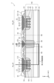
- FIG. 1 is a schematic cross-sectional view showing an example of a structure of a semiconductor device according to an embodiment.
- FIG. 2A is a schematic plan view showing an example of a structure of a semiconductor device according to an embodiment.
- FIG. 2B is a schematic plan view showing an example of the structure of the semiconductor device according to the embodiment.
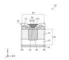
- FIG. 3 is a schematic cross-sectional view showing an example of a structure of a semiconductor device according to a modified example of the embodiment.
- FIG. 4A is a schematic plan view of a general unit configuration of a first transistor according to an embodiment.
- FIG. 4B is a schematic perspective view of a general unit configuration of a first transistor according to the embodiment.
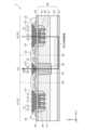
- FIG. 5A is a schematic cross-sectional view showing a first conduction path of a semiconductor device according to an embodiment.
- FIG. 5B is a schematic cross-sectional view showing a second conduction path of the semiconductor device according to the embodiment.
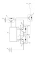
- FIG. 6 is a circuit diagram showing an example of use of the semiconductor device according to the embodiment.
- FIG. 7 is a circuit diagram showing an example of use of a semiconductor device according to a comparative example.
- FIG. 8A is a schematic plan view illustrating an example of the structure of a transistor according to a comparative example.
- FIG. 8B is a schematic plan view illustrating an example of the structure of a transistor according to a comparative example.
- FIG. 9A is a schematic plan view illustrating an example of the structure of a transistor according to a comparative example.
- FIG. 9B is a schematic plan view illustrating an example of the structure of a transistor according to a comparative example.
- FIG. 10 is a schematic plan view showing an example of a structure of a transistor according to a modified example of the embodiment.
- FIG. 11 is a schematic plan view showing an example of a structure of a transistor according to a modified example of the embodiment.
- FIG. 12A is a schematic plan view illustrating an example of a structure of a transistor according to a modified example of the embodiment.
- FIG. 12B is a schematic plan view illustrating an example of a structure of a transistor according to a modification of the embodiment.
- FIG. 13 is a schematic plan view showing a drain contact region of a semiconductor device according to an embodiment.
- FIG. 14 is a graph showing the relationship between the arrangement of the drain contact region of the semiconductor device according to the embodiment and the conduction resistance of each of the first conduction path and the second conduction path.
- a and B are electrically connected includes cases where A and B are directly connected via wiring, where A and B are directly connected without wiring, and where A and B are indirectly connected via a resistance component (resistance element, resistance wiring).
- the semiconductor device according to an embodiment is a chip size package (CSP) type semiconductor device that has a dual configuration in which two vertical MOS (Metal Oxide Semiconductor) transistors are formed on a semiconductor substrate and can be mounted face-down.
- the two vertical MOS transistors are power transistors, so-called trench MOS type FETs (Field Effect Transistors).
- FIG. 1 is a schematic cross-sectional view showing an example of the structure of a semiconductor device 1 according to an embodiment.
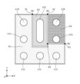
- FIGS. 2A and 2B are schematic plan views showing an example of the structure of a semiconductor device 1 according to an embodiment.
- the size and shape of the semiconductor device 1 in FIGS. 2A and 2B are examples.
- the size, shape, and arrangement of the pads and electrodes are also examples.
- FIG. 1 shows a cross section of semiconductor device 1 taken along line I-I in FIG. 2A.
- the semiconductor device 1 has a semiconductor substrate 32, a metal layer 41, and a low-concentration impurity layer 33 formed on the semiconductor substrate 32.
- the semiconductor substrate 32 and the low-concentration impurity layer 33 are collectively referred to as a semiconductor layer 40.
- the semiconductor substrate 32 is disposed on the back surface side of the semiconductor layer 40 and is made of silicon of a first conductivity type containing an impurity of a first concentration.
- the semiconductor layer 40 has a low-concentration impurity layer 33 of the first conductivity type formed in contact with the semiconductor substrate 32 and containing an impurity of a second concentration lower than the first concentration.
- the low-concentration impurity layer 33 is formed on the semiconductor substrate 32 by, for example, epitaxial growth.
- the semiconductor device 1 has a first vertical MOS transistor 10 (hereinafter also referred to as “transistor 10") entirely formed within a first region A1 of the semiconductor layer 40, and a second vertical MOS transistor 20 (hereinafter also referred to as “transistor 20”) entirely formed within a second region A2 of the semiconductor layer 40.
- transistor 10 first vertical MOS transistor
- transistor 20 second vertical MOS transistor
- a transistor 10 formed entirely within the first region A1 means that, in a planar view, all of the elements constituting the transistor 10 are contained within the first region A1 and are not contained in any region that is not the first region A1.
- a transistor 20 formed entirely within the second region A2 means that, in a planar view, all of the elements constituting the transistor 20 are contained within the second region A2 and are not contained in any region that is not the second region A2.
- the surface side of the semiconductor layer 40 is divided into a first region A1, a second region A2, and a third region A3 in a plan view, which do not overlap with each other and are not disposed separately.
- the fact that the first region A1, the second region A2, and the third region A3 are not disposed separately means that the first region A1, the second region A2, and the third region A3 do not include any enclaves.
- a virtual boundary line 90 that divides the first region A1, the second region A2, and the third region A3 is shown by a dotted line.
- the dotted line indicating the boundary line 90 is shown extending to the outside of the semiconductor layer 40, but the actual boundary line 90 terminates at the outer periphery of the semiconductor layer 40 in a plan view (for convenience, the ends of the boundary line 90 are shown as P1, P2, and P3, respectively, in FIG. 2A and FIG. 2B).
- the boundary line 90 will be described later.
- the dashed lines indicating the first region A1, the second region A2, and the third region A3 are not exactly aligned with the outer periphery of the semiconductor layer 40 and the boundary line 90 for ease of understanding, but are drawn with some space between them.
- the outer periphery of the first region A1, the outer periphery of the second region A2, and the outer periphery of the third region A3 essentially coincide with the outer periphery of the semiconductor layer 40 and the boundary line 90.
- the metal layer 41 is formed in contact with the back side of the semiconductor layer 40, and may be made of silver (Ag) or copper (Cu), as a non-limiting example. Note that the metal layer 41 may contain trace amounts of elements other than metals that are mixed in as impurities during the manufacturing process of the metal material.
- a first body region 18 of a second conductivity type different from the first conductivity type is formed in a first region A1 of the low-concentration impurity layer 33.
- a first source region 14 of the first conductivity type is formed in the first body region 18.
- the first region A1 also has a plurality of first gate trenches 17 formed to a depth that penetrates from the upper surface of the semiconductor layer 40 through the first source region 14 and the first body region 18 to a portion of the low-concentration impurity layer 33, and a first gate conductor 15 is formed on the first gate insulating film 16 inside the first gate trench 17.
- the first gate conductor 15 is a buried gate electrode buried inside the semiconductor layer 40.
- the first gate conductor 15 is electrically connected to the first gate electrode 19 via the first gate wiring (see FIG. 2B).
- the first source electrode 11 consists of a portion 12 and a portion 13, and the portion 12 is connected to the first source region 14 and the first body region 18 via the portion 13.
- the portion 12 of the first source electrode 11 is a layer that is joined with the solder during reflow in face-down mounting, and may be made of a metal material including, by way of non-limiting example, any one or more of nickel, titanium, tungsten, and palladium.
- the surface of the portion 12 may be plated with gold or the like.
- Part 13 of the first source electrode 11 is a layer that connects part 12 and the semiconductor layer 40, and may be made of a metal material including, by way of non-limiting example, any one or more of aluminum, copper, gold, and silver.
- a second body region 28 of a second conductivity type different from the first conductivity type is formed in the second region A2 of the low-concentration impurity layer 33.
- a second source region 24 of the first conductivity type is formed in the second body region 28.
- the second region A2 also has a plurality of second gate trenches 27 formed to a depth that penetrates from the upper surface of the semiconductor layer 40 through the second source region 24 and the second body region 28 to a portion of the low-concentration impurity layer 33, and a second gate conductor 25 is formed on the second gate insulating film 26 inside the second gate trench 27.
- the second gate conductor 25 is a buried gate electrode buried inside the semiconductor layer 40.
- the second gate conductor 25 is electrically connected to the second gate electrode 29 via the second gate wiring (see FIG. 2B).
- the second source electrode 21 consists of a portion 22 and a portion 23, and the portion 22 is connected to the second source region 24 and the second body region 28 via the portion 23.
- the portion 22 of the second source electrode 21 is a layer that is joined with the solder during reflow in face-down mounting, and may be made of a metal material including, by way of non-limiting example, any one or more of nickel, titanium, tungsten, and palladium.
- the surface of the portion 22 may be plated with gold or the like.
- Part 23 of the second source electrode 21 is a layer that connects part 22 and the semiconductor layer 40, and may be made of a metal material including, by way of non-limiting example, any one or more of aluminum, copper, gold, and silver.
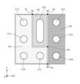
- FIG. 2B shows the state of the semiconductor device 1 according to this embodiment immediately after the formation of the portion 13 of the first source electrode 11, the first gate electrode 19, the first gate wiring, the portion 23 of the second source electrode 21, the second gate electrode 29, the second gate wiring, and the portion 83 of the surface drain electrode 81 (described later) on the surface side of the semiconductor layer 40.
- pads that would not be visible at this point are shown with dotted lines in FIG. 2B.
- the first body region 18 is covered with an interlayer insulating layer 34 having an opening, and a portion 13 of the first source electrode 11 is provided that is connected to the first source region 14 through the opening in the interlayer insulating layer 34.
- the interlayer insulating layer 34 and the portion 13 of the first source electrode 11 are covered with a passivation layer 35 having an opening, and a portion 12 is provided that is connected to the portion 13 of the first source electrode 11 through the opening in the passivation layer 35.
- the second body region 28 is covered with an interlayer insulating layer 34 having an opening, and a portion 23 of the second source electrode 21 is provided that is connected to the second source region 24 through the opening in the interlayer insulating layer 34.
- the interlayer insulating layer 34 and the portion 23 of the second source electrode 21 are covered with a passivation layer 35 having an opening, and a portion 22 is provided that is connected to the portion 23 of the second source electrode 21 through the opening in the passivation layer 35.
- the first source pad 111 and the second source pad 121 respectively refer to the areas where the first source electrode 11 and the second source electrode 21 are partially exposed on the surface of the semiconductor device 1, i.e., the terminal portions.
- the first gate pad 119 and the second gate pad 129 respectively refer to the areas where the first gate electrode 19 and the second gate electrode 29 are partially exposed on the surface of the semiconductor device 1, i.e., the terminal portions.
- first source pads 111 and second source pads 121 are not necessarily limited to the number illustrated in FIG. 2A.
- the shapes of the first source pads 111 and second source pads 121 are not necessarily limited to the circular shapes illustrated in FIG. 2A, and may be rectangular or elliptical, for example.
- the arrangement of the first source pads 111 and second source pads 121 is not necessarily limited to the arrangement illustrated in FIG. 2A.
- first gate pads 119 and second gate pads 129 are not necessarily limited to the number illustrated in FIG. 2A, and may be two or more.
- the shapes of first gate pads 119 and second gate pads 129 are not necessarily limited to the circular shapes illustrated in FIG. 2A, and may be rectangular or elliptical, for example.
- the semiconductor substrate 32 and the area of the low-concentration impurity layer 33 immediately above the semiconductor substrate 32 are a common drain region that is shared by the first drain region of transistor 10 and the second drain region of transistor 20.
- the metal layer 41 is a common drain electrode (hereinafter referred to as the back surface drain electrode 41) in which the first drain electrode of the transistor 10 and the second drain electrode of the transistor 20 are commonized.
- a drain pull-up region 38 is formed in the third region A3 of the semiconductor layer 40, which pulls up the current from the common drain region (semiconductor substrate 32) and the back surface drain electrode 41 to the front surface side of the semiconductor layer 40.
- the drain pull-up region 38 contains impurities at a concentration higher than the first concentration of the semiconductor substrate 32, and is of the first conductivity type.
- the drain pull-up region 38 is formed to a depth from the top surface of the semiconductor layer 40 to a part of the semiconductor substrate 32.
- a surface drain electrode 81 that connects to the drain pull-up region 38 is formed at a position that is included in the third region A3 in a plan view.
- the modification "surface” is intended to distinguish it from the back surface drain electrode 41, which is the same drain electrode.
- the surface drain electrode 81 consists of a portion 82 and a portion 83, and the portion 82 is connected to the low-concentration impurity layer 33 and/or the drain pull-up region 38 via the portion 83.
- Part 82 of the surface drain electrode 81 is a layer that is joined with solder during reflow in face-down mounting, and may be made of a metal material including, by way of non-limiting example, any one or more of nickel, titanium, tungsten, and palladium.
- the surface of part 82 may be plated with gold or the like.
- Part 83 of the surface drain electrode 81 is a layer that connects part 82 to the semiconductor layer 40, and may be made of a metal material including, by way of non-limiting example, any one or more of aluminum, copper, gold, and silver.
- the drain pull-up region 38 is covered with an interlayer insulating layer 34 having an opening, and a portion 83 of a surface drain electrode 81 is provided that connects to the drain pull-up region 38 through the opening in the interlayer insulating layer 34.
- the interlayer insulating layer 34 and the portion 83 of the surface drain electrode 81 are covered with a passivation layer 35 having an opening, and a portion 82 is provided that connects to the portion 83 of the surface drain electrode 81 through the opening in the passivation layer 35.
- the drain pad 151 refers to the area where the surface drain electrode 81 is partially exposed on the surface of the semiconductor device 1, i.e., the terminal portion.
- the number of drain pads 151 is not necessarily limited to the number illustrated in FIG. 2A.
- the shape of the drain pads 151 is not necessarily limited to the elliptical shape illustrated in FIG. 2A, and may be, for example, rectangular or circular.
- the drain pad 151 is arranged so that its center coincides with the center of the third region A3, but even if the center of the drain pad 151 and the center of the third region A3 are arranged not to coincide with each other, there is no impediment to obtaining the effects of the present disclosure.
- the center of a shape in a planar view is defined as follows. For circular shapes such as first source pad 111 and first gate pad 119 in FIG. 2A, it refers to the center. For rectangular shapes such as third region A3, it refers to the intersection of the diagonals. For oval shapes such as drain pad 151, it refers to the intersection of the axis of line symmetry extending in the longitudinal direction and the axis of line symmetry extending in the width direction.
- drain contact region 39 is the overlapping portion of the region where the drain pull-up region 38 is exposed on the surface side of the semiconductor layer 40 and the opening region of the interlayer insulating layer 34.
- the width of the drain pull-up region 38 is larger than the width of the opening of the interlayer insulating layer 34 (the area where the drain pull-up region 38 is exposed on the surface side of the semiconductor layer 40 in a plan view is larger than the opening area of the interlayer insulating layer 34), so the drain contact region 39 coincides with the opening region of the interlayer insulating layer 34 in a plan view.
- Figure 3 is a schematic cross-sectional view showing a portion of a semiconductor device 1A according to a first modification in which only the shape of the drain pull-up region 38 has been modified from that of the semiconductor device 1 according to the embodiment.
- the width of the drain pull-up region 38 may be smaller than the opening width of the interlayer insulating layer 34, but in such a case, the drain contact region 39 coincides with the region where the drain pull-up region 38 is exposed on the surface side of the semiconductor layer 40 in a plan view.
- the drain contact region 39 may be large in plan view to reduce the conductive resistance.
- the area where the portion 83 of the surface drain electrode 81 contacts the semiconductor layer 40 in the third region A3 (the area of the opening region of the interlayer insulating layer 34) and the area where the drain pull-up region 38 is exposed on the surface side of the semiconductor layer 40 may be roughly the same size, although there may be a difference in size.
- the first region A1 and the second region A2 are disposed with the third region A3 in between.
- the first region A1 and the second region A2 sandwiching the third region A3 means that the first region A1 and the third region A3 are adjacent to each other with no other region in between, and the second region A2 and the third region A3 are adjacent to each other with no other region in between. Therefore, in a plan view of the semiconductor layer 40, the third region A3 is adjacent to both the first region A1 and the second region A2.
- the length of the boundary line 90 may be referred to as the facing length.
- the boundary line 90 between the first region A1 and the third region A3 may be considered as an imaginary line that traces the center position of the gap between the portion 13 of the first source electrode 11 and the portion 83 of the surface drain electrode 81. It may also be considered as the gap itself, although it has a finite width. Even in the case of the gap, it can be recognized as a line by the naked eye or when viewed at low magnification.
- the boundary line 90 between the first region A1 and the third region A3 is a dotted line from P1 to P4.
- the boundary line 90 between the second region A2 and the third region A3 may be considered as an imaginary line that traces the center position of the gap between the portion 23 of the second source electrode 21 and the portion 83 of the surface drain electrode 81. It may also be considered as the gap itself, although it has a finite width.
- the boundary line 90 between the second region A2 and the third region A3 is the dotted line from P2 to P4.
- the boundary line 90 between them may be considered as an imaginary line that traces the center position of the gap between the portion 13 of the first source electrode 11 and the portion 23 of the second source electrode 21. It may also be considered as the gap itself, although it has a finite width.
- the boundary line 90 between the first region A1 and the second region A2 is the dotted line from P4 to P3.
- the area a1 of the first region A1 in a plan view is larger than the area a2 of the second region A2 in a plan view (a1>a2).
- the first region A1 and the second region A2 do not halve the area remaining after removing the third region A3 from the semiconductor layer 40 in a plan view (a1 ⁇ a2). Therefore, the length of the boundary line 90 between the first region A1 and the third region A3 (opposing length, the length from P1 to P4) is longer than the length of the boundary line 90 between the second region A2 and the third region A3 (opposing length, the length from P2 to P4).
- the first region A1 is arranged so that it has an outer periphery that at least partially coincides with each of the four sides of the semiconductor layer 40.
- the second region A2 is arranged so that its outer periphery only partially coincides with two of the four sides of the rectangular outer periphery of the semiconductor layer 40.
- the second gate pad 129 is placed closest to a corner formed by two sides of the outer periphery of the second region A2 that are not adjacent to the first region A1.
- the second gate pad 129 is placed in the second region A2 farthest from the boundary line 90 with the first region A1. Note that in the embodiment, the pad and the corner being closest to each other means that no other pad is placed between the pad and the corner.
- first gate pad 119 is located opposite the second gate pad 129 across the drain pad 151 in a plan view.
- FIGS. 4A and 4B are schematic plan and perspective views, respectively, of an approximate unit configuration of transistor 10 or transistor 20 that is repeatedly formed in the X and Y directions of semiconductor device 1 according to an embodiment.
- semiconductor substrate 32 and metal layer 41, passivation layer 35 and first source electrode 11 or second source electrode 21, and interlayer insulating layer 34 are not shown in FIGS. 4A and 4B.
- the Y direction is parallel to the surface of the semiconductor layer 40 and is the direction in which the first gate trench 17 extends.
- the X direction is parallel to the surface of the semiconductor layer 40 and perpendicular to the Y direction.
- the Z direction is perpendicular to both the X and Y directions and indicates the height direction of the semiconductor device.
- the transistor 10 has a first connection portion 18a that electrically connects the first body region 18 and the first source electrode 11.
- the first connection portion 18a is a region of the first body region 18 in which the first source region 14 is not formed, and is of the same second conductivity type as the first body region 18.
- the first source region 14 and the first connection portion 18a are alternately and periodically arranged in the Y direction. The same is true for the transistor 20.
- the first conductivity type is N-type and the second conductivity type is P-type, with the first source region 14, the second source region 24, the drain pull-up region 38, the semiconductor substrate 32, and the low-concentration impurity layer 33 being N-type semiconductors, and the first body region 18, the first connection portion 18a, the second body region 28, and the second connection portion 28a being P-type semiconductors.
- 5A and 5B are schematic cross-sectional views showing the conduction paths of the semiconductor device 1 according to the embodiment.
- the embodiment does not assume driving that conducts electricity along a path from the first source pad 111 to the second source pad 121 and/or the reverse path.
- the conduction path through which a current flows from the first source pad 111 in the first region A1 as an inlet to the drain pad 151 in the third region A3 as an outlet is called the first conduction path.
- the conduction path through which a current flows from the second source pad 121 in the second region A2 as an inlet to the drain pad 151 in the third region A3 as an outlet is called the second conduction path.
- a current flows as follows.
- a high voltage is applied to the first source electrode 11 and a low voltage is applied to the surface drain electrode 81, and a voltage equal to or greater than the threshold is applied (ON control) to the first gate electrode 19 (first gate conductor 15) with the first source electrode 11 as a reference, forming a conduction channel near the first gate insulating film 16 in the first body region 18.
- the PN junction at the contact surface between the second body region 28 and the low-concentration impurity layer 33 in the transistor 20 functions as a body diode. This prevents conduction from the first source pad 111 to the second source pad 121.
- a current flows as follows.
- a high voltage is applied to the second source electrode 21 and a low voltage is applied to the surface drain electrode 81, and a voltage equal to or greater than the threshold is applied (ON control) to the second gate electrode 29 (second gate conductor 25) with the second source electrode 21 as a reference, forming a conduction channel near the second gate insulating film 26 in the second body region 28.
- the second source electrode 21 When the potential of the second source electrode 21 is sufficiently high relative to the potential of the surface drain electrode 81, it is not necessary to apply (ON control) a voltage equal to or higher than the threshold voltage to the second gate electrode 29 (second gate conductor 25). In this case, a conductive channel is not formed near the second gate insulating film 26 in the second body region 28, but a current flows through the path of the second source electrode 21 - second connection portion 28a - second body region 28 - low concentration impurity layer 33 - semiconductor substrate 32 - metal layer 41 - semiconductor substrate 32 - drain pull-up region 38 - surface drain electrode 81, and the semiconductor device 1 becomes conductive.
- the PN junction at the contact surface between the first body region 18 and the low-concentration impurity layer 33 in the transistor 10 functions as a body diode. This prevents conduction from the second source pad 121 to the first source pad 111.
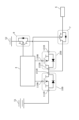
- FIG. 6 is a circuit diagram showing a part of a power supply circuit that supplies current to a load 6 from a first power supply 51 and a second power supply 52, each of which is detachable, via a semiconductor device 1 according to an embodiment.
- the potential of the load 6 is taken as a reference, and the potential of the first power supply 51 is assumed to be higher than the potential of the second power supply 52.
- the semiconductor device 1 is installed to merge two power systems, a high-potential power supply from a first power supply 51 and a lower-potential power supply from a second power supply 52, and combine them into one system toward a downstream load 6, which is at a low potential.
- I1 [A] The maximum value of the current flowing due to power supply from the first power supply 51, which has a high potential, is I1 [A]
- I2 [A] the maximum value of the current flowing due to power supply from the second power supply 52, which has a lower potential than the first power supply 51.
- I1 and I2 can be considered to be the specified maximum current values in the first conduction path and the second conduction path, respectively, described in the product data sheet of the semiconductor device 1 according to the embodiment.
- the relationship between the potentials of the first power supply 51 and the second power supply 52 is I1>I2.
- the first power supply 51 side which conducts a relatively large current I1 is connected to the first source pad 111 of the transistor 10, which has a large area in a planar view in the semiconductor device 1
- the second power supply 52 side which conducts a relatively small current I2 is connected to the second source pad 121 of the transistor 20, which has a small area in a planar view in the semiconductor device 1.
- a switching element 7 (e.g., a single-type vertical MOS transistor) is connected between the semiconductor device 1 and the load 6.
- a switching element 8 (e.g., a single-type vertical MOS transistor) is connected between the semiconductor device 1 and the second power supply 52.
- a control IC 4 is connected to the switching elements 7 and 8 and the semiconductor device 1, and the control IC 4 individually controls the ON/OFF of the switching elements 7, 8, transistor 10 and transistor 20.
- the control IC 4 controls the switching element 7 to be turned on and the transistor 20 to be turned off, and power is supplied from the first power supply 51 to the load 6 via the first conduction path in the semiconductor device 1. Furthermore, if the control IC 4 controls the transistor 10 to be turned on, the conduction resistance in the first conduction path can be reduced.
- the first conduction path is a conduction path inside the semiconductor device 1, and as explained above, is a conduction path through which current flows with the first source pad 111 of the transistor 10 as an inlet and the drain pad 151 as an outlet.
- the transistor 20 is controlled to be OFF. Because the transistor 20 is controlled to be OFF, the current flowing due to the power supply from the first power source 51 can be prevented from flowing toward the second power source 52.
- the control IC 4 controls the switching element 7 to be turned on and the transistor 10 to be turned off, and power is supplied from the second power supply 52 to the load 6 via the second conduction path in the semiconductor device 1. If the control IC 4 further controls the transistor 20 to be turned on, the conduction resistance in the second conduction path can be reduced.
- the second conduction path is a conduction path inside the semiconductor device 1, and as explained above, is a conduction path through which current flows with the second source pad 121 of the transistor 20 as an inlet and the drain pad 151 as an outlet.
- the transistor 10 is controlled to be OFF. Because the transistor 10 is controlled to be OFF, the current flowing due to power supply from the second power source 52 can be prevented from flowing toward the first power source 51.
- the control IC 4 first controls the switching element 8 to be turned OFF, creating a state in which power is supplied only from the first power supply 51. This is because the first power supply 51 has a higher potential and is therefore dominant in power supply. Furthermore, the switching element 7 is controlled to be turned ON and the transistor 20 is controlled to be turned OFF, thereby supplying power from the first power supply 51 to the load 6 via the first conduction path. If the control IC 4 controls the transistor 10 to be turned ON, the conduction resistance in the first conduction path can be reduced.
- FIG. 7 shows a comparative example in which the semiconductor device 1 according to the embodiment is not used in the power supply circuit shown in Fig. 6.
- a single-configuration vertical MOS transistor 10B (hereinafter referred to as transistor 10B) whose structure is shown in the schematic plan views of Figs. 8A and 8B
- a single-configuration vertical MOS transistor 20B (hereinafter referred to as transistor 20B) whose structure is shown in the schematic plan views of Figs. 9A and 9B are used instead of the semiconductor device 1 according to the embodiment.
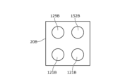
- transistors 10B and 20B components that are the same as those in the semiconductor device 1 according to the embodiment are indicated by adding the letter B to the reference numerals of the corresponding components. However, for the purpose of distinction, different reference numerals are used for the drain pads of transistor 10B (drain pad 151B) and transistor 20B (drain pad 152B).
- FIGS. 8B and 9B show the state immediately after the source electrode portion 13B (23B), gate electrode 19B (29B), gate wiring, and surface drain electrode portion 83B are formed on the surface side of the semiconductor layer 40.
- pads that would not be visible at this point are shown with dotted lines in FIGS. 8B and 9B.
- the area in a plan view of portion 13B of the source electrode of transistor 10B is the same as the area in a plan view of portion 13 of the first source electrode 11 of transistor 10 provided in semiconductor device 1 according to the embodiment. Therefore, the conduction resistance of the path from first power source 51 through transistor 10B to load 6 in FIG. 7 can be considered to be equivalent to the conduction resistance of the first conduction path of semiconductor device 1 according to the embodiment in FIG. 6.
- the area in a plan view of portion 23B of the source electrode of transistor 20B is the same as the area in a plan view of portion 23 of second source electrode 21 of transistor 20 provided in semiconductor device 1 according to the embodiment. Therefore, the conduction resistance of the path from second power source 52 via transistor 20B to load 6 in FIG. 7 can be regarded as being equivalent to the conduction resistance of the second conduction path of semiconductor device 1 according to the embodiment in FIG. 6.
- the transistor 20B is controlled to be OFF, and the current flowing due to the power supply from the first power supply 51 is prevented from flowing toward the second power supply 52.
- the transistor 10B is controlled to be ON by applying a voltage equal to or higher than the threshold value to the gate pad 119B, and the current flowing due to the power supply from the first power supply 51 flows in from the source pad 111B of the transistor 10B and flows out from the drain pad 151B.
- the area of the transistor 10B in a plan view (the area of the source electrode portion 13B) is relatively large because the current flowing due to the power supply from the first power supply 51 is relatively large.
- the transistor 10B when only the second power supply 52 is connected (the first power supply 51 is not present in FIG. 7), the transistor 10B is controlled to be OFF, and the current flowing due to the power supply from the second power supply 52 is prevented from flowing toward the first power supply 51.
- the transistor 20B is controlled to be ON by applying a voltage equal to or higher than the threshold value to the gate pad 129B, and the current flowing due to the power supply from the second power supply 52 flows in from the source pad 121B of the transistor 20B and flows out from the drain pad 152B.
- the area of the transistor 20B in a plan view (the area of the source electrode portion 23B) is relatively small because the current flowing due to the power supply from the second power supply 52 is relatively small.
- transistor 10B performs the same function as transistor 10 provided in the semiconductor device 1 of the embodiment in the power supply circuit of FIG. 6.
- transistor 20B performs the same function as transistor 20 provided in the semiconductor device 1 of the embodiment in the power supply circuit of FIG. 6.
- transistors 10B and 20B each have a drain pad (151B, 152B) in plan view, so the structure requires a certain area.
- the circuit board mounting the power supply circuit shown in FIG. 6 by using the semiconductor device 1 according to the embodiment, it is possible to integrate the transistors 10B and 20B according to the comparative example. This eliminates the need for a certain installation margin between the transistors 10B and 20B that was necessary in the circuit board mounting the power supply circuit according to the comparative example, and further, the drain pads (151B, 152B) that the transistors 10B and 20B each have can be made common, thereby reducing the area required for the circuit board.
- the circuit board mounting the power supply circuit shown in FIG. 6 it is also possible to reduce the size of the board itself compared to the comparative example, and it is also possible to mount other components in the resulting surplus portion.
- the semiconductor device 1 is therefore a chip-size package type semiconductor device 1 capable of face-down mounting, and has a semiconductor substrate 32 on the back side, and is provided with a semiconductor layer 40 divided into three regions, a first region A1, a second region A2, and a third region A3, which do not overlap with each other in a planar view of the semiconductor device 1 and are not disposed in a dispersed manner, a first vertical MOS transistor 10 entirely formed in the first region A1 of the semiconductor layer 40, a second vertical MOS transistor 20 entirely formed in the second region A2 of the semiconductor layer 40, and a metal layer 41 formed in contact with the back side of the semiconductor layer 40, and the semiconductor substrate 32 is a common drain region of the first vertical MOS transistor 10 and the second vertical MOS transistor 20, and in a planar view
- the semiconductor device 1 is characterized in that the first source pad 111 and the first gate pad 119 of the first vertical MOS transistor 10 are formed in a position included in the first region A1, the second source pad 121 and the second gate pad pad
- the first conduction path has the first source pad 111 in the first region A1 as an inlet and the drain pad 151 in the third region A3 as an outlet. Therefore, if the first region A1 and the third region A3 are adjacent in a planar view, the first conduction path is shortened, which is convenient because the conduction resistance can be reduced.
- the second conduction path has the second source pad 121 in the second region A2 as an inlet and the drain pad 151 in the third region A3 as an outlet. Therefore, if the second region A2 and the third region A3 are adjacent in a planar view, the second conduction path is shortened, which is convenient because the conduction resistance can be reduced.
- first region A1 and the second region A2 are disposed on either side of the third region A3, and that the third region A3 is adjacent to the first region A1 and the second region A2.
- the opposing length between the first region A1 and the third region A3 is longer than the opposing length between the second region A2 and the third region A3 in a planar view.
- FIG. 10 is a schematic plan view of the semiconductor device 1 according to the embodiment in which the ratio of the layout of the first region A1 and the second region A2 is changed.
- the semiconductor layer 40 may be rectangular in plan view, and the first region A1 may be disposed so as to have an outer periphery that at least partially coincides with each of the four sides of the semiconductor layer 40.
- FIG. 11 is a schematic plan view of the semiconductor device 1 according to the embodiment in which the ratio of the layout of the first region A1 and the second region A2 is changed.
- the location where the second gate electrode 29 is installed cannot contribute to conduction. For this reason, it is desirable to install the second gate electrode 29 in the second region A2 as far away as possible from any location that may obstruct the second conduction path in plan view. Then, it is desirable to install the second gate electrode 29 as far away as possible from the boundary line 90 between the second region A2 and the third region A3, where the current density is highest in the second conduction path.
- the second gate electrode 29, i.e., the second gate pad 129 be placed closest to the corner formed by the two sides of the outer periphery of the second region A2 that are not adjacent to the third region A3.
- the second gate pad 129 is placed closest to the upper right corner in a plan view.
- Figures 12A and 12B are schematic plan views in which the positions of the first gate electrode 19, the first gate pad 119, the second gate electrode 29, and the second gate pad 129 are changed from modified example 2 of the semiconductor device 1 according to the embodiment.
- Figure 12B shows the state immediately after the first source electrode portion 13, the second source electrode portion 23, the first gate electrode 19, the second gate electrode 29, the first gate wiring, the second gate wiring, and the surface drain electrode portion 83 are formed on the surface side of the semiconductor layer.
- pads that would not be visible at this point are shown with dotted lines in Figure 12B.
- the second gate pad 129 is disposed in the second region A2 so as to be closest to the boundary line 90 (dotted line from P3 to P4) between the first region A1 and the second region A2 in a plan view. This makes it possible to make full use of the region along the boundary line 90 (dotted line from P2 to P4) between the second region A2 and the third region A3, where the current density is highest in the second conduction path.
- the second gate pad 129 is arranged so that, in a plan view, it is closest to the corner that is furthest from the drain pad 151 among the corners that form the outer periphery of the second region A2. This allows the area along the boundary line 90 (dotted line from P2 to P4) between the second region A2 and the third region A3 to be widely utilized.
- the first gate pad 119 is arranged so that, in a plan view, it is closest to the corner that is furthest from the drain pad 151 among the corners that form the outer periphery of the first region A1. This allows the area along the boundary line 90 (dotted line from P1 to P4) between the first region A1 and the third region A3 to be widely utilized.
- the area a1 of the transistor 10 forming the first conduction path in a planar view is larger than the area a2 of the transistor 20 forming the second conduction path in a planar view. Therefore, the first conduction path has a lower conduction resistance and is suitable for passing a relatively large current.
- the conduction resistance R1 [ ⁇ ] of the first conduction path may be determined taking into account the maximum value I1 [A] of the current flowing due to the power supply from the first power source 51.
- the conduction resistance R2 [ ⁇ ] of the second conduction path may be determined taking into account the maximum value I2 [A] of the current flowing due to the power supply from the second power source 52. Therefore, in the semiconductor device 1 according to the embodiment, it is desirable to determine the areas of the transistors 10 and 20 so that the conduction resistances suitable for the first conduction path and the second conduction path are respectively realized.
- the area a2 of the transistor 20 in a planar view calculated as above is too small, the ESD (Electrostatic Discharge) resistance of the transistor 20 decreases, and the semiconductor device 1 as a whole may not be able to maintain the ESD guarantee value. If the area a2 of the transistor 20 in a planar view is increased so that the ESD guarantee value can be maintained, the conduction resistance of the second conduction path will decrease excessively, making it difficult to limit the current from the second power supply 52 to the desired magnitude.
- the inventors therefore discovered that by appropriately designing the size (area) and position of the drain contact region 39 in the third region A3 in a plan view of the semiconductor device 1, it is possible to control the conduction resistance in the second conduction path separately from the area a2 in a plan view of the transistor 20.
- the semiconductor device 1 according to the embodiment will be described as having the area a2 of the transistor 20 in a plan view increased as much as necessary to maintain the ESD guarantee value. In other words, the semiconductor device 1 according to the embodiment will be considered as having an excessively low conductive resistance in the second conductive path.
- FIG. 13 is a schematic plan view of the semiconductor device 1 shown in FIG. 2B, showing only the third region A3.
- the drain contact region 39 is a region where the drain pull-up region 38 and the portion 83 of the surface drain electrode 81 are connected. Therefore, the drain contact region 39 is a part contained within the third region A3 in a plan view.
- both the third region A3 and the drain contact region 39 are rectangular in plan view.
- the direction along the short side of the rectangular third region A3 in plan view (X direction in FIG. 13) is defined as the first direction
- the direction along the long side of the third region A3 is defined as the second direction.
- the first and second directions are perpendicular to each other.
- the side length of the third region A3 in the first direction is L1 [ ⁇ m]
- the side length in the second direction is L2 [ ⁇ m].
- the side length of the drain contact region 39 in the first direction is l1 [ ⁇ m]
- the side length in the second direction is l2 [ ⁇ m].
- the inventors set the conditions for the area of the drain contact region 39 in a plan view as l1 ⁇ L1/4 and l2 ⁇ L2.
- l2 is a dimension smaller than L2 by the installation margins at both ends in the second direction.
- the condition l1 ⁇ L1/4 is set in order to reduce the area of the drain contact region 39 to at least 1/4 of the area of the third region A3, thereby making it possible to adjust the position of the drain contact region 39 in a plan view by adjusting the distance from the second region A2.
- FIG. 14 shows a graph plotting the results of calculating the conduction resistance R1 of the first conduction path when transistor 10 is controlled to be ON and transistor 20 is controlled to be OFF, and the conduction resistance R2 of the second conduction path when transistor 20 is controlled to be ON and transistor 10 is controlled to be OFF.
- the conduction resistance R1 of the first conduction path is indicated by a circular marker and plotted on the left vertical axis.
- the conduction resistance R2 of the second conduction path is indicated by a diamond marker and plotted on the right vertical axis.
- the horizontal axis in FIG. 14 is the position along the first direction in the third region A3 in a plan view. The position is based on the left end of the third region A3 in FIG. 13, that is, on the boundary line 90 between the first region A1 and the third region A3. The horizontal axis is plotted based on the position of the center of the drain contact region 39.
- the arrows shown at the top of Figure 14 indicate, from the left in the first direction, the reference position, the position L1/4 from the reference, the position L1/2 from the reference, the position 3 x L1/4 from the reference, and the position L1 from the reference, i.e., the positions on the boundary line 90 between the third area A3 and the second area A2.
- the third area A3 is divided into four areas at the above positions so that they have equal areas, and from left to right in the first direction, these are called the fourth area, the fifth area, the sixth area, and the seventh area.
- the semiconductor device 1 is a square with sides of 1.5 mm in plan view, and the division of the first area A1, second area A2, and third area A3 and the shapes and arrangement of each pad and electrode are as shown in FIG. 2A and FIG. 2B, respectively.
- the data is plotted on the horizontal axis at a certain distance from the left and right ends because, in plan view, an installation margin is added to portion 83 of surface drain electrode 81 within third region A3.
- drain contact region 39 when drain contact region 39 is placed near the center of third region A3 in plan view, both R1 and R2 are extremely small.
- near the center refers to the fifth or sixth region.
- drain contact region 39 is in, for example, the fourth region, this means that in plan view, the center of drain contact region 39 is in the fourth region. This does not necessarily mean that the entire area of drain contact region 39 is contained within the fourth region.
- the semiconductor substrate 32 is of a first conductivity type containing a first concentration of impurities
- the semiconductor layer 40 has a low concentration impurity layer 33 of the first conductivity type formed on and in contact with the semiconductor substrate 32 and containing a second concentration of impurities lower than the first concentration of impurities
- a drain pull-up region 38 of the first conductivity type containing a higher concentration of impurities than the first concentration of impurities and connected to the common drain region (semiconductor substrate 32) is formed in the third region A3 of the semiconductor layer 40 in a planar view
- a portion 83 of a surface drain electrode 81 that contacts the surface of the semiconductor layer 40 and connects to the drain pull-up region 38 is formed at a position included in the third region A3 in a planar view
- the area of the drain contact region 39 where the portion 83 of the surface drain electrode 81 and the drain pull-up region 38 are connected is desirably 1 ⁇ 4 or less of the area of the third
- the shape of the drain contact region 39 in a plan view is a roughly rectangular shape with its longitudinal direction in the second direction, almost the same effect can be obtained.
- the third region A3 is rectangular, and the maximum width l1 of the drain contact region 39 in a first direction parallel to the short side L1 of the third region A3 is smaller than the maximum width l2 of the drain contact region 39 in a second direction perpendicular to the first direction and parallel to the long side L2 of the third region A3 in a plan view, and it is desirable that in a plan view, the maximum width l1 of the drain contact region 39 in the first direction is 1/4 or less of the length of the short side L1 of the third region.
- the conduction resistance R1 of the first conduction path is almost constant and extremely small.
- the conduction resistance R2 of the second conduction path increases as the drain contact region 39 is positioned closer to the fourth region. Therefore, by placing the drain contact region 39 in the fifth region, it is possible to increase only R2 while keeping R1 reduced.
- the third region is divided into four equal regions, a fourth region, a fifth region, a sixth region, and a seventh region, each of which has the same area in the first direction, and in a plan view, the fourth region, the fifth region, the sixth region, and the seventh region are arranged in this order along the first direction from the boundary line 90 between the first region A1 and the third region A3 to the boundary line 90 between the second region A2 and the third region A3, and in a plan view, the center of the drain contact region 39 may be located in the fifth region.
- the drain contact region 39 is located in the fifth region, near the border with the fourth region.
- the drain contact region 39 may be located including the border between the fourth and fifth regions.
- the third region is divided into four equal regions, a fourth region, a fifth region, a sixth region, and a seventh region, each of which has an equal area in the first direction, and in a plan view, the fourth region, the fifth region, the sixth region, and the seventh region are arranged in this order along the first direction from the boundary line 90 between the first region A1 and the third region A3 to the boundary line 90 between the second region A2 and the third region A3, and in a plan view, the center of the drain contact region 39 may be located in the fourth region.
- both R1 and R2 are maintained at almost minimum values, which is convenient when it is desired to achieve low values for both R1 and R2.
- the third region is divided into four equal regions, a fourth region, a fifth region, a sixth region, and a seventh region, each of which has the same area in the first direction, and in a plan view, the fourth region, the fifth region, the sixth region, and the seventh region are arranged in this order along the first direction from the boundary line 90 between the first region A1 and the third region A3 to the boundary line 90 between the second region A2 and the third region A3, and in a plan view, the center of the drain contact region 39 may be located in the sixth region.
- the conductive resistance R1 of the first conductive path and the conductive resistance R2 of the second conductive path can be adjusted by the size (area) of the drain contact region 39 and its installation position. Even if the second region A2 is expanded to achieve the required ESD resistance, particularly in the transistor 20 having a small area, the conductive resistance R2 of the second conductive path can be achieved at a desired high value. Therefore, the current flowing through the first conductive path and the current flowing through the second conductive path can be set to the desired magnitude.
- a semiconductor device equipped with the vertical MOS transistor of the present invention can be widely used as a device for controlling the conduction state of a current path.
Landscapes
- Semiconductor Integrated Circuits (AREA)
- Insulated Gate Type Field-Effect Transistor (AREA)
Abstract
半導体装置(1)は、裏面側に半導体基板(32)を有し、半導体装置(1)の平面視において互いに重複しない第1の領域(A1)と第2の領域(A2)と第3の領域(A3)との3つの領域に分けられた半導体層(40)と、半導体層(40)の第1の領域(A1)に形成された第1の縦型MOSトランジスタ(10)と、半導体層(40)の第2の領域(A2)に形成された第2の縦型MOSトランジスタ(20)と、半導体装置(1)の平面視において、第3の領域(A3)に内包される位置に、半導体基板(32)に接続されたドレインパッド(151)と、を備え、半導体装置(1)の平面視において、第3の領域(A3)は、第1の領域(A1)および第2の領域(A2)に挟まれ、半導体装置(1)の平面視において、第1の領域(A1)の面積は、第2の領域(A2)の面積よりも大きい。
Description
本開示は、半導体装置に関し、特には、チップサイズパッケージ型の半導体装置に関する。
仕様の電流値が異なる2系統を、1系統に取りまとめる電気回路で縦型MOSトランジスタが用いられることがある。
縦型MOSトランジスタを用いた回路の小型化が求められている。
上記の課題を解決するために、本開示の一態様に係る半導体装置は、フェイスダウン実装が可能なチップサイズパッケージ型の半導体装置であって、裏面側に半導体基板を有し、半導体装置の平面視において、互いに重複しない第1の領域、第2の領域、第3の領域の、それぞれ分散して配置されない3つの領域に分けられた半導体層と、前記半導体層の前記第1の領域に、その全体が形成された第1の縦型MOSトランジスタと、前記半導体層の前記第2の領域に、その全体が形成された第2の縦型MOSトランジスタと、前記半導体層の裏面に接触して形成された金属層と、を備え、前記半導体基板は、前記第1の縦型MOSトランジスタおよび前記第2の縦型MOSトランジスタの共通ドレイン領域であり、前記平面視において、前記第1の領域に内包される位置に、前記第1の縦型MOSトランジスタの第1のソースパッドおよび第1のゲートパッドが形成され、前記平面視において、前記第2の領域に内包される位置に、前記第2の縦型MOSトランジスタの第2のソースパッドおよび第2のゲートパッドが形成され、前記平面視において、前記第3の領域に内包される位置に、前記共通ドレイン領域に接続されたドレインパッドが形成され、前記半導体層の前記平面視において、前記第1の領域および前記第2の領域は、前記第3の領域を挟んで配置され、前記平面視において、前記第3の領域は、前記第1の領域および前記第2の領域に隣接し、前記平面視において、前記第1の領域の面積は、前記第2の領域の面積よりも大きい半導体装置であることを特徴とする。
上記デュアル構成の縦型MOSトランジスタを、例えば仕様の電流値が異なる2つの導通経路を1つに合流させる回路に用いることで、従来に比べて回路が必要とする面積を削減することができる。
したがって、上記構成の半導体装置によると、縦型MOSトランジスタを用いた回路の小型化を実現することができる。
以下で説明する実施の形態は、いずれも本開示の一具体例を示すものである。以下の実施の形態で示される数値、形状、材料、構成要素、構成要素の配置位置および接続形態などは、一例であり、本開示を限定する主旨ではない。
本開示において、「AとBとが電気的に接続される」とは、AとBとが配線を介して直接的に接続される場合と、AとBとが配線を介さず直接的に接続される場合と、AとBとが抵抗成分(抵抗素子、抵抗配線)を介して間接的に接続される場合と、を含む。
(実施の形態)
[1.半導体装置の構造]
以下、実施の形態に係る半導体装置の構造について説明する。実施の形態に係る半導体装置は、半導体基板に2つの縦型MOS(Metal Oxide Semiconductor)トランジスタを形成したデュアル構成の、フェイスダウン実装が可能なチップサイズパッケージ(Chip Size Package:CSP)型の半導体デバイスである。上記2つの縦型MOSトランジスタは、パワートランジスタであり、いわゆる、トレンチMOS型FET(Field Effect Transistor)である。
[1.半導体装置の構造]
以下、実施の形態に係る半導体装置の構造について説明する。実施の形態に係る半導体装置は、半導体基板に2つの縦型MOS(Metal Oxide Semiconductor)トランジスタを形成したデュアル構成の、フェイスダウン実装が可能なチップサイズパッケージ(Chip Size Package:CSP)型の半導体デバイスである。上記2つの縦型MOSトランジスタは、パワートランジスタであり、いわゆる、トレンチMOS型FET(Field Effect Transistor)である。
図1は、実施の形態に係る半導体装置1の構造の一例を示す断面模式図である。図2A、図2Bは実施の形態に係る半導体装置1の構造の一例を示す平面模式図である。図2A、図2Bにおいて半導体装置1の大きさや形状は一例である。またパッド、電極の大きさや形状および配置も一例である。
図1は、図2AのI-Iに沿って半導体装置1を切断したときの切断面である。
図1に示すように、半導体装置1は、半導体基板32と、金属層41と、半導体基板32上に形成された低濃度不純物層33と、を有する。本開示では半導体基板32と低濃度不純物層33とを合わせて半導体層40と称する。
半導体基板32は、半導体層40の裏面側に配置され、第1の濃度の不純物を含む第1導電型のシリコンからなる。半導体層40は、半導体基板32に接触して形成された、第1の濃度よりも低い第2の濃度の不純物を含む、第1導電型の低濃度不純物層33を有する。低濃度不純物層33は、例えば、エピタキシャル成長により半導体基板32上に形成される。
図1および図2Aに示すように、半導体装置1は、半導体層40の第1の領域A1内にその全体が形成された第1の縦型MOSトランジスタ10(以下、「トランジスタ10」とも称する)と、半導体層40の第2の領域A2内にその全体が形成された第2の縦型MOSトランジスタ20(以下、「トランジスタ20」とも称する)と、を有する。
第1の領域A1内にその全体が形成されたトランジスタ10とは、平面視で、トランジスタ10を構成する要素のすべてが第1の領域A1の内部に含まれていて、第1の領域A1ではない領域には含まれないことを意味する。同様に、第2の領域A2内にその全体が形成されたトランジスタ20とは、平面視で、トランジスタ20を構成する要素のすべてが第2の領域A2の内部に含まれていて、第2の領域A2ではない領域には含まれないことを意味する。
図2Aに示すように、平面視において半導体層40の表面側は、互いに重複せず、それぞれ分散して配置されない、第1の領域A1、第2の領域A2、第3の領域A3に分けられる。ここで、第1の領域A1と第2の領域A2と第3の領域A3とがそれぞれ分散して配置されないとは、第1の領域A1と第2の領域A2と第3の領域A3とがそれぞれ飛び地を伴わないことを意味する。図2Aでは第1の領域A1、第2の領域A2、第3の領域A3をそれぞれ区分する仮想的な境界線90を点線で示している。分かりやすさのために、境界線90を示す点線は半導体層40の外部まで延長して示しているが、実際の境界線90は平面視で、半導体層40の外周において終端する(図2A、図2Bにおいては便宜的に、境界線90の終端をそれぞれP1、P2、P3として示している)。境界線90については後述する。
なお、図2Aにおいて、第1の領域A1、第2の領域A2、第3の領域A3を示す破線は分かりやすさのため半導体層40の外周および境界線90とは厳密に一致させず、若干の余白を置いて内側に示しているが、実質的に第1の領域A1の外周と第2の領域A2の外周と第3の領域A3の外周とは、半導体層40の外周および境界線90と一致するものである。
金属層41は、半導体層40の裏面側に接触して形成され、限定されない一例として、銀(Ag)もしくは銅(Cu)で構成されてもよい。なお、金属層41には、金属材料の製造工程において不純物として混入する金属以外の元素が微量に含まれていてもよい。
図1および図2Aに示すように、低濃度不純物層33の第1の領域A1には、第1導電型と異なる第2導電型の第1のボディ領域18が形成されている。第1のボディ領域18には、第1導電型の第1のソース領域14が形成されている。
また第1の領域A1には、半導体層40の上面から第1のソース領域14および第1のボディ領域18を貫通して低濃度不純物層33の一部までの深さに形成された複数の第1のゲートトレンチ17が形成されており、さらに第1のゲート導体15が、第1のゲートトレンチ17の内部で第1のゲート絶縁膜16上に形成されている。第1のゲート導体15は、半導体層40の内部に埋め込まれた埋め込みゲート電極である。第1のゲート導体15は、第1のゲート配線を介して第1のゲート電極19と電気的に接続される(図2B参照)。
第1のソース電極11は部分12と部分13とからなり、部分12は、部分13を介して第1のソース領域14および第1のボディ領域18に接続されている。
第1のソース電極11の部分12は、フェイスダウン実装におけるリフロー時にはんだと接合される層であり、限定されない一例として、ニッケル、チタン、タングステン、パラジウムのうちのいずれか1つ以上を含む金属材料で構成されてもよい。部分12の表面には、金などのめっきが施されてもよい。
第1のソース電極11の部分13は、部分12と半導体層40とを接続する層であり、限定されない一例として、アルミニウム、銅、金、銀のうちのいずれか1つ以上を含む金属材料で構成されてもよい。
同様に、低濃度不純物層33の第2の領域A2には、第1導電型と異なる第2導電型の第2のボディ領域28が形成されている。第2のボディ領域28には、第1導電型の第2のソース領域24が形成されている。
また第2の領域A2には、半導体層40の上面から第2のソース領域24および第2のボディ領域28を貫通して低濃度不純物層33の一部までの深さに形成された複数の第2のゲートトレンチ27が形成されており、さらに第2のゲート導体25が、第2のゲートトレンチ27の内部で第2のゲート絶縁膜26上に形成されている。第2のゲート導体25は、半導体層40の内部に埋め込まれた埋め込みゲート電極である。第2のゲート導体25は、第2のゲート配線を介して第2のゲート電極29と電気的に接続される(図2B参照)。
第2のソース電極21は部分22と部分23とからなり、部分22は、部分23を介して第2のソース領域24および第2のボディ領域28に接続されている。
第2のソース電極21の部分22は、フェイスダウン実装におけるリフロー時にはんだと接合される層であり、限定されない一例として、ニッケル、チタン、タングステン、パラジウムのうちのいずれか1つ以上を含む金属材料で構成されてもよい。部分22の表面には、金などのめっきが施されてもよい。
第2のソース電極21の部分23は、部分22と半導体層40とを接続する層であり、限定されない一例として、アルミニウム、銅、金、銀のうちのいずれか1つ以上を含む金属材料で構成されてもよい。
図2Bは、本実施の形態に係る半導体装置1の、半導体層40の表面側に第1のソース電極11の部分13、第1のゲート電極19、第1のゲート配線、第2のソース電極21の部分23、第2のゲート電極29、第2のゲート配線、そして後述する表面ドレイン電極81の部分83、が形成された直後の様子を示したものである。図2Bでは分かりやすさのため、この時点では見えないはずのパッドを点線で示している。
図1に示すように、第1のボディ領域18は開口を有する層間絶縁層34で覆われ、層間絶縁層34の開口を通して第1のソース領域14に接続される第1のソース電極11の部分13が設けられている。層間絶縁層34および第1のソース電極11の部分13は開口を有するパッシベーション層35で覆われ、パッシベーション層35の開口を通して第1のソース電極11の部分13に接続される部分12が設けられている。
同様に、第2のボディ領域28は開口を有する層間絶縁層34で覆われ、層間絶縁層34の開口を通して第2のソース領域24に接続される第2のソース電極21の部分23が設けられている。層間絶縁層34および第2のソース電極21の部分23は開口を有するパッシベーション層35で覆われ、パッシベーション層35の開口を通して第2のソース電極21の部分23に接続される部分22が設けられている。
したがって、第1のソースパッド111および第2のソースパッド121は、図2Bからも分かるように、それぞれ、第1のソース電極11および第2のソース電極21が半導体装置1の表面に部分的に露出した領域、すなわち端子の部分を指す。同様に、第1のゲートパッド119および第2のゲートパッド129は、それぞれ、第1のゲート電極19および第2のゲート電極29が半導体装置1の表面に部分的に露出した領域、すなわち端子の部分を指す。
第1のソースパッド111および第2のソースパッド121の数は、それぞれ必ずしも図2Aに例示された数に限定されない。また第1のソースパッド111および第2のソースパッド121の形状は、それぞれ図2Aに例示された円形状に限定される必要はなく、例えば矩形状や楕円形状であってもよい。また第1のソースパッド111および第2のソースパッド121の配置は、それぞれ図2Aに例示された配置に限定されない。
第1のゲートパッド119および第2のゲートパッド129の数は、それぞれ必ずしも図2Aに例示された数に限定されず、2以上の複数であってもよい。また第1のゲートパッド119および第2のゲートパッド129の形状は、それぞれ図2Aに例示された円形状に限定される必要はなく、例えば矩形状や楕円形状であってもよい。
トランジスタ10およびトランジスタ20の上記の構成により、半導体基板32と、低濃度不純物層33のうち半導体基板32の直上近傍の範囲は、トランジスタ10の第1のドレイン領域およびトランジスタ20の第2のドレイン領域とが共通化された、共通ドレイン領域である。
金属層41はトランジスタ10の第1のドレイン電極およびトランジスタ20の第2のドレイン電極が共通化された、共通ドレイン電極(以下、裏面ドレイン電極41と称する)である。
図1に示すように、半導体層40の第3の領域A3内には、共通ドレイン領域(半導体基板32)および裏面ドレイン電極41からの電流を半導体層40の表面側に引き上げる、ドレイン引き上げ領域38が形成されている。ドレイン引き上げ領域38は、半導体基板32の第1の濃度よりも高い濃度の不純物を含み、第1導電型である。ドレイン引き上げ領域38は半導体層40の上面から半導体基板32の一部までの深さに形成されている。
半導体層40の表面側において、平面視において、第3の領域A3に内包される位置に、ドレイン引き上げ領域38と接続する表面ドレイン電極81が形成されている。表面という修飾は、同じドレイン電極である裏面ドレイン電極41と区別するためのものである。
表面ドレイン電極81は部分82と部分83とからなり、部分82は、部分83を介して低濃度不純物層33および/またはドレイン引き上げ領域38と接続されている。
表面ドレイン電極81の部分82は、フェイスダウン実装におけるリフロー時にはんだと接合される層であり、限定されない一例として、ニッケル、チタン、タングステン、パラジウムのうちのいずれか1つ以上を含む金属材料で構成されてもよい。部分82の表面には、金などのめっきが施されてもよい。
表面ドレイン電極81の部分83は、部分82と半導体層40とを接続する層であり、限定されない一例として、アルミニウム、銅、金、銀のうちのいずれか1つ以上を含む金属材料で構成されてもよい。
ドレイン引き上げ領域38は、開口を有する層間絶縁層34で覆われ、層間絶縁層34の開口を通してドレイン引き上げ領域38と接続する表面ドレイン電極81の部分83が設けられている。層間絶縁層34および表面ドレイン電極81の部分83は、開口を有するパッシベーション層35で覆われ、パッシベーション層35の開口を通して表面ドレイン電極81の部分83に接続される部分82が設けられている。
したがって図2Bに示すように、ドレインパッド151は、表面ドレイン電極81が半導体装置1の表面に部分的に露出した領域、すなわち端子の部分を指す。
ドレインパッド151の数は、必ずしも図2Aに例示された数に限定されない。またドレインパッド151の形状は、図2Aに例示された楕円形状に限定される必要はなく、例えば矩形状や円形状であってもよい。
図2Aに示す例では、ドレインパッド151は、その中心と第3の領域A3の中心とが一致するように配置されているが、ドレインパッド151の中心と第3の領域A3の中心が一致しない配置であっても本開示の効果を得るのになんら差し支えることはない。
なお本開示では、平面視における形状の中心を次にように定義する。図2Aにおける第1のソースパッド111および第1のゲートパッド119のように円形状のものはその中心のことをいう。第3の領域A3のように矩形状のものは、その対角線の交点のことをいう。ドレインパッド151のように長円形状のものは、その長手方向に伸びる、線対称の対称軸と、その幅方向に伸びる、線対称の対象軸との交点のことをいう。
ドレイン引き上げ領域38と表面ドレイン電極81の部分83とが接触する部分をドレインコンタクト領域39とよぶ。ドレインコンタクト領域39は、平面視で、ドレイン引き上げ領域38が半導体層40の表面側に露出する領域と、層間絶縁層34の開口領域との重複部分である。図1に示す例のような場合は、ドレイン引き上げ領域38の幅が層間絶縁層34の開口の幅よりも大きい(平面視でドレイン引き上げ領域38が半導体層40の表面側で露出する面積の方が層間絶縁層34の開口面積よりも大きい)ために、ドレインコンタクト領域39は、平面視で層間絶縁層34の開口領域と一致することになる。
図3は、実施の形態に係る半導体装置1から、ドレイン引き上げ領域38の形状だけが変形した変形例1に係る半導体装置1Aのうち、一部を切り取って示した断面模式図である。図3に示すように、ドレイン引き上げ領域38の幅は層間絶縁層34の開口幅よりも小さくてもよいが、このような場合のドレインコンタクト領域39は、平面視でドレイン引き上げ領域38が半導体層40の表面側で露出する領域と一致する。
いずれにせよ、平面視でのドレインコンタクト領域39は導通抵抗の低減のため、広い面積であってよい。典型的には、平面視で、第3の領域A3において表面ドレイン電極81の部分83が半導体層40と接触する面積(層間絶縁層34の開口領域の面積)と、ドレイン引き上げ領域38が半導体層40の表面側で露出する面積とは、大小の差はあれ、同程度に広くてよい。
さて図2Aに示すように、第1の領域A1と第2の領域A2とは、第3の領域A3を挟んで配置される。実施の形態おいて、第1の領域A1と第2の領域A2が、第3の領域A3を挟むとは、第1の領域A1と第3の領域A3とが間に他の領域を挟まずに隣接し、さらに第2の領域A2と第3の領域A3とが間に他の領域を挟まずに隣接するということである。したがって半導体層40の平面視において、第3の領域A3は、第1の領域A1および第2の領域A2に、共に隣接する。
平面視である領域とある領域が、隣接する、とは、対向する、という意味と同じであり、互いの間にある境界線90において、互いの外周が一致するということである。以降、境界線90の長さのことを対向長ということがある。
図2Bに示すように、第1の領域A1と第3の領域A3との境界線90は、第1のソース電極11の部分13と、表面ドレイン電極81の部分83との間隔の中央位置をたどる仮想線と捉えてよい。また有限の幅となるが当該間隔そのものと捉えてもよい。当該間隔の場合であっても、肉眼あるいは低倍率での外観では線として認識することができる。第1の領域A1と第3の領域A3との境界線90は、図2A、図2Bに示す例においては、P1からP4までの点線である。
同様に、第2の領域A2と第3の領域A3との境界線90は、第2のソース電極21の部分23と、表面ドレイン電極81の部分83との間隔の中央位置をたどる仮想線と捉えてよい。また有限の幅となるが当該間隔そのものと捉えてもよい。第2の領域A2と第3の領域A3との境界線90は、図2A、図2Bに示す例においては、P2からP4までの点線である。
図2Bにあるように、第1の領域A1と第2の領域A2とが隣接する場合は、両者の境界線90は、第1のソース電極11の部分13と、第2のソース電極21の部分23との間隔の中央位置をたどる仮想線と捉えてよい。また有限の幅となるが当該間隔そのものと捉えてもよい。第1の領域A1と第2の領域A2との境界線90は、図2A、図2Bに示す例においては、P4からP3までの点線である。
図2A、図2Bに示すように、第1の領域A1の平面視での面積a1は、第2の領域A2の平面視での面積a2よりも大きい(a1>a2)。同じことだが、第1の領域A1および第2の領域A2は、平面視において、半導体層40から第3の領域A3を除いた残りの面積を二等分していない(a1≠a2)。したがって第1の領域A1と第3の領域A3との境界線90の長さ(対向長、P1からP4までの長さ)は、第2の領域A2と第3の領域A3との境界線90の長さ(対向長、P2からP4までの長さ)よりも長い。
図2A、図2Bに示す実施の形態の例では、平面視において、第1の領域A1は、半導体層40の4辺のそれぞれと少なくとも一部が一致する外周を有するように配置されている。これに対して第2の領域A2は、その外周が、矩形状である半導体層40の外周4辺のうち2辺とのみ、それぞれ一部で一致するところがあるように配置されている。
図2A、図2Bに示す実施の形態の例では、平面視で、第2のゲートパッド129は、第2の領域A2の外周辺のうち、第1の領域A1とは隣接しない2辺で形成される角部に最近接して設置されている。第2のゲートパッド129は第2の領域A2において、第1の領域A1との境界線90から最も離れて設置されている。なお実施の形態において、パッドと角部が最近接するとは、当該パッドと当該角部との間に、他のいかなるパッドも設置されないことをいう。
また、第1のゲートパッド119は平面視において、ドレインパッド151を挟んで第2のゲートパッド129と対向する位置に設置されている。
図4Aおよび図4Bは、それぞれ、実施の形態に係る半導体装置1のX方向およびY方向に繰り返し形成される、トランジスタ10またはトランジスタ20の略単位構成の、平面模式図および斜視模式図である。図4Aおよび図4Bでは、分かりやすさのために半導体基板32と金属層41、さらにパッシベーション層35と第1のソース電極11または第2のソース電極21、層間絶縁層34は図示していない。
なおY方向とは、半導体層40の表面と平行し、第1のゲートトレンチ17が延在する方向である。またX方向とは、半導体層40の表面と平行し、Y方向に直交する方向のことをいう。Z方向とは、X方向にもY方向にも共に直交し、半導体装置の高さ方向を示す方向のことをいう。
図4Aおよび図4Bに示すように、トランジスタ10には、第1のボディ領域18と第1のソース電極11とを電気的に接続する第1の接続部18aが備わる。第1の接続部18aは、第1のボディ領域18のうち、第1のソース領域14が形成されていない領域であり、第1のボディ領域18と同じ第2導電型である。第1のソース領域14と第1の接続部18aとは、Y方向に沿って交互に、かつ周期的に繰り返し配置される。トランジスタ20についても同様である。
本開示に係る半導体装置1では、第1導電型をN型、第2導電型をP型として、第1のソース領域14、第2のソース領域24、ドレイン引き上げ領域38、半導体基板32、および、低濃度不純物層33はN型半導体であり、かつ、第1のボディ領域18、第1の接続部18a、第2のボディ領域28および第2の接続部28aはP型半導体であるとする。
[2.半導体装置の動作]
以下、図5A、図5Bを用いて半導体装置1の第1の導通経路および第2の導通経路と、半導体装置1の駆動の仕方について説明する。図5A,図5Bは、実施の形態に係る半導体装置1の導通経路を示す断面模式図である。
以下、図5A、図5Bを用いて半導体装置1の第1の導通経路および第2の導通経路と、半導体装置1の駆動の仕方について説明する。図5A,図5Bは、実施の形態に係る半導体装置1の導通経路を示す断面模式図である。
実施の形態に係る半導体装置1では、電流は、第1の領域A1の第1のソースパッド111または第2の領域A2の第2のソースパッド121のどちらか一方を流入口として、共通ドレイン領域および裏面ドレイン電極41を経由し、第3の領域A3のドレインパッド151を流出口として流れることを想定する。すなわち実施の形態では、第1のソースパッド111から第2のソースパッド121への経路、および/または、その逆の経路で導通する駆動を想定しない。
半導体装置1において、第1の領域A1の第1のソースパッド111を流入口とし、第3の領域A3のドレインパッド151を流出口として電流が流れる導通経路を、第1の導通経路とよぶ。第2の領域A2の第2のソースパッド121を流入口とし、第3の領域A3のドレインパッド151を流出口として電流が流れる導通経路を、第2の導通経路とよぶ。
図5Aに示す第1の導通経路では、以下のように電流が流れる。半導体装置1において、第1のソース電極11に高電圧および表面ドレイン電極81に低電圧を印加し、第1のソース電極11を基準として第1のゲート電極19(第1のゲート導体15)にしきい値以上の電圧を印加(ON制御)することで、第1のボディ領域18中の第1のゲート絶縁膜16の近傍に導通チャネルを形成する。導通チャネルが形成されると、第1のソース電極11-第1のソース領域14-第1のボディ領域18に形成された導通チャネル-低濃度不純物層33-半導体基板32-金属層41-半導体基板32-ドレイン引き上げ領域38-表面ドレイン電極81という経路で電流が流れて、半導体装置1が導通状態となる。
表面ドレイン電極81の電位に対して第1のソース電極11の電位が十分に高いとき、第1のゲート電極19(第1のゲート導体15)には、必ずしもしきい値以上の電圧を印加(ON制御)しなくてもよい。この場合、第1のボディ領域18中の第1のゲート絶縁膜16の近傍に導通チャネルは形成されないが、第1のソース電極11-第1の接続部18a-第1のボディ領域18-低濃度不純物層33-半導体基板32-金属層41-半導体基板32-ドレイン引き上げ領域38-表面ドレイン電極81という経路で電流が流れて、半導体装置1が導通状態となる。
上記はいずれも第1の導通経路である。後者の場合、第1のボディ領域18と低濃度不純物層33との接触面にPN接合があるため、相対的に導通抵抗が高くなる。前者の場合は導通チャネルを経由するので導通抵抗が相対的に低くなる。
いずれにしても、第1の導通経路を導通させる際には、トランジスタ20における第2のボディ領域28と低濃度不純物層33との接触面にあるPN接合をボディダイオードとして機能させていることに留意すべきである。これがあるために第1のソースパッド111から第2のソースパッド121へ導通することがない。半導体装置1において第1の導通経路だけを使用する場合には、トランジスタ20の、第2のゲート電極29(第2のゲート導体25)には、しきい値以上の電圧を印加しないこと(OFF制御)が望ましい。
図5Bに示す第2の導通経路では、以下のように電流が流れる。半導体装置1において、第2のソース電極21に高電圧および表面ドレイン電極81に低電圧を印加し、第2のソース電極21を基準として第2のゲート電極29(第2のゲート導体25)にしきい値以上の電圧を印加(ON制御)することで、第2のボディ領域28中の第2のゲート絶縁膜26の近傍に導通チャネルを形成する。導通チャネルが形成されると、第2のソース電極21-第2のソース領域24-第2のボディ領域28に形成された導通チャネル-低濃度不純物層33-半導体基板32-金属層41-半導体基板32-ドレイン引き上げ領域38-表面ドレイン電極81という経路で電流が流れて、半導体装置1が導通状態となる。
表面ドレイン電極81の電位に対して第2のソース電極21の電位が十分に高いとき、第2のゲート電極29(第2のゲート導体25)には、必ずしもしきい値以上の電圧を印加(ON制御)しなくてもよい。この場合、第2のボディ領域28中の第2のゲート絶縁膜26の近傍に導通チャネルは形成されないが、第2のソース電極21-第2の接続部28a-第2のボディ領域28-低濃度不純物層33-半導体基板32-金属層41-半導体基板32-ドレイン引き上げ領域38-表面ドレイン電極81という経路で電流が流れて、半導体装置1が導通状態となる。
上記はいずれも第2の導通経路である。後者の場合、第2のボディ領域28と低濃度不純物層33との接触面にPN接合があるため、相対的に導通抵抗が高くなる。前者の場合は導通チャネルを経由するので導通抵抗が相対的に低くなる。
いずれにしても、第2の導通経路を導通させる際には、トランジスタ10における第1のボディ領域18と低濃度不純物層33との接触面にあるPN接合をボディダイオードとして機能させていることに留意すべきである。これがあるために第2のソースパッド121から第1のソースパッド111へ導通することがない。半導体装置1において第2の導通経路だけを使用する場合には、トランジスタ10の、第1のゲート電極19(第1のゲート導体15)には、しきい値以上の電圧を印加しないこと(OFF制御)が望ましい。
なお図5Aおよび図5Bで示したように、第1の導通経路においても第2の導通経路においても、半導体装置1内部を水平方向に流れる電流は、そのほとんどは抵抗率の低い金属層41を経由するが、一部には半導体基板32を流れることもある。
[3.半導体装置の使用例]
図6は、それぞれ脱着が可能な第1の電源51と第2の電源52とから、実施の形態に係る半導体装置1を経由して負荷6へ電流を流す給電回路の一部を示した回路図である。ここでは負荷6の電位を基準として、第1の電源51の電位が、第2の電源52の電位よりも高電位であるとする。
図6は、それぞれ脱着が可能な第1の電源51と第2の電源52とから、実施の形態に係る半導体装置1を経由して負荷6へ電流を流す給電回路の一部を示した回路図である。ここでは負荷6の電位を基準として、第1の電源51の電位が、第2の電源52の電位よりも高電位であるとする。
実施の形態に係る半導体装置1は、高電位である第1の電源51からの給電と、それよりは低い電位である第2の電源52からの給電との2系統を合流し、低電位である下流の負荷6へ向けて1系統にまとめる機能を果たすように設置される。
高電位である第1の電源51からの給電によって流れる電流の最大値をI1[A]とし、第1の電源51の電位よりは低電位である第2の電源52からの給電によって流れる電流の最大値をI2[A]とする。I1、I2は実施の形態に係る半導体装置1の製品データシートに記載される、それぞれ第1の導通経路および第2の導通経路における仕様最大電流値であると捉えて差し支えない。
第1の電源51と第2の電源52の電位の関係から、I1>I2の関係がある。相対的に大きい電流I1が導通する、第1の電源51側は、半導体装置1において平面視での面積が大きいトランジスタ10の、第1のソースパッド111に接続されており、相対的に小さい電流I2が導通する、第2の電源52側は、半導体装置1において平面視での面積が小さいトランジスタ20の、第2のソースパッド121に接続されている。
なお、半導体装置1と負荷6との間には、スイッチング素子7(例えば、シングル型の縦型MOSトランジスタ)が接続されている。また半導体装置1と第2の電源52との間には、スイッチング素子8(例えば、シングル型の縦型MOSトランジスタ)が接続されている。スイッチング素子7、スイッチング素子8および半導体装置1には制御IC4が接続されており、制御IC4によってスイッチング素子7、スイッチング素子8、トランジスタ10およびトランジスタ20のON/OFFがそれぞれ個別に制御される。
はじめに第1の電源51だけを接続し、第2の電源52を接続しない状態(図6において第2の電源52が存在しない状態)について説明する。このとき、制御IC4によってスイッチング素子7がON制御され、かつトランジスタ20がOFF制御され、半導体装置1内の第1の導通経路を経て、第1の電源51から負荷6への給電がおこなわれる。さらに制御IC4によってトランジスタ10がON制御されれば、第1の導通経路における導通抵抗を低減することができる。
第1の導通経路とは半導体装置1の内部の導通経路であり、先に説明したようにトランジスタ10の第1のソースパッド111を流入口とし、ドレインパッド151を流出口として電流が流れる導通経路である。第1の導通経路だけを導通する際にはトランジスタ20はOFF制御される。トランジスタ20がOFF制御されているために、第1の電源51からの給電によって流れる電流が、第2の電源52の側へ向かうことを防止できる。
次に第2の電源52だけを接続し、第1の電源51を接続しない状態(図6において第1の電源51が存在しない状態)について説明する。このとき、制御IC4によってスイッチング素子7がON制御され、かつトランジスタ10がOFF制御され、半導体装置1内の第2の導通経路を経て、第2の電源52から負荷6への給電がおこなわれる。さらに制御IC4によってトランジスタ20がON制御されれば、第2の導通経路における導通抵抗を低減することができる。
第2の導通経路とは半導体装置1の内部の導通経路であり、先に説明したようにトランジスタ20の第2のソースパッド121を流入口とし、ドレインパッド151を流出口として電流が流れる導通経路である。第2の導通経路だけを導通する際にはトランジスタ10はOFF制御される。トランジスタ10がOFF制御されているために、第2の電源52からの給電によって流れる電流が、第1の電源51の側へ向かうことを防止できる。
第1の電源51と第2の電源52とを共に接続する場合(図6の状態)では、制御IC4によって、まずスイッチング素子8がOFF制御され、第1の電源51だけから給電される状態を構成する。これは第1の電源51の方が高電位であり、給電に優位であるためである。さらにスイッチング素子7がON制御され、トランジスタ20がOFF制御されることで、第1の電源51から第1の導通経路を経由した、負荷6への給電がおこなわれる。制御IC4によってトランジスタ10がON制御されれば、第1の導通経路における導通抵抗を低減することができる。
[4.半導体装置の効果]
図6に示した給電回路で、実施の形態に係る半導体装置1を使用しない場合の比較例を図7に示した。比較例においては、実施の形態に係る半導体装置1の代わりに、例えば、図8A、図8Bに構造の一例を平面模式図で示したシングル構成の縦型MOSトランジスタ10B(以下、トランジスタ10Bという)と、図9A、図9Bに構造の一例を平面模式図で示したシングル構成の縦型MOSトランジスタ20B(以下、トランジスタ20Bという)と、をそれぞれ使用する。
図6に示した給電回路で、実施の形態に係る半導体装置1を使用しない場合の比較例を図7に示した。比較例においては、実施の形態に係る半導体装置1の代わりに、例えば、図8A、図8Bに構造の一例を平面模式図で示したシングル構成の縦型MOSトランジスタ10B(以下、トランジスタ10Bという)と、図9A、図9Bに構造の一例を平面模式図で示したシングル構成の縦型MOSトランジスタ20B(以下、トランジスタ20Bという)と、をそれぞれ使用する。
トランジスタ10Bとトランジスタ20Bで、実施の形態に係る半導体装置1が有するのと同様の構成要素については、対応する構成要素の符号にBを追加して示している。ただし区別のため、ドレインパッドについては、トランジスタ10B(が有するドレインパッド151B)とトランジスタ20B(が有するドレインパッド152B)とで符号を分けている。
図8B、図9Bでは、本実施の形態に係る半導体装置1の平面模式図(図2B)で示したのと同じように、半導体層40の表面側に、ソース電極の部分13B(23B)、ゲート電極19B(29B)、ゲート配線、そして表面ドレイン電極の部分83B、が形成された直後の様子を示したものである。図8B、図9Bでは分かりやすさのため、この時点では見えないはずのパッドを点線で示している。
トランジスタ10Bのソース電極の部分13Bの平面視での面積と、実施の形態に係る半導体装置1に備わるトランジスタ10が有する第1のソース電極11の部分13の平面視での面積とは同じである。したがって、図7において第1の電源51からトランジスタ10Bを経由して負荷6へ流れる経路の導通抵抗は、図6における実施の形態に係る半導体装置1の第1の導通経路の導通抵抗と同等であると捉えて差し支えない。
またトランジスタ20Bのソース電極の部分23Bの平面視での面積と、実施の形態に係る半導体装置1に備わるトランジスタ20が有する第2のソース電極21の部分23の平面視での面積とは同じである。したがって、図7において第2の電源52からトランジスタ20Bを経由して負荷6へ流れる経路の導通抵抗は、図6における実施の形態に係る半導体装置1の第2の導通経路の導通抵抗と同等であると捉えて差し支えない。
図7に示す給電回路において、第1の電源51のみが接続される(図7で第2の電源52が存在しない)場合、トランジスタ20BはOFF制御されて、第1の電源51からの給電によって流れる電流が、第2の電源52の側へ向かうことを防ぐ。トランジスタ10Bはゲートパッド119Bにしきい値以上の電圧が印加されてON制御され、第1の電源51からの給電によって流れる電流は、トランジスタ10Bのソースパッド111Bから流入し、ドレインパッド151Bから流出する。図8A、図8Bに示すように、トランジスタ10Bの平面視での面積(ソ―ス電極の部分13Bの面積)が相対的に大きいのは、第1の電源51からの給電によって流れる電流が相対的に大きいためである。
図7の給電回路において、第2の電源52のみが接続される(図7で第1の電源51が存在しない)場合、トランジスタ10BはOFF制御されて、第2の電源52からの給電によって流れる電流が、第1の電源51の側へ向かうことを防ぐ。トランジスタ20Bはゲートパッド129Bにしきい値以上の電圧が印加されてON制御され、第2の電源52からの給電によって流れる電流は、トランジスタ20Bのソースパッド121Bから流入し、ドレインパッド152Bから流出する。図9A、図9Bに示すように、トランジスタ20Bの平面視での面積(ソ―ス電極の部分23Bの面積)が相対的に小さいのは、第2の電源52からの給電によって流れる電流が相対的に小さいためである。
以上のように、図7に示す比較例に係る給電回路では、トランジスタ10Bは図6の給電回路における、実施の形態に係る半導体装置1に備わるトランジスタ10と同じ機能を果たす。同様に、図7に示す比較例に係る給電回路では、トランジスタ20Bは図6の給電回路における、実施の形態に係る半導体装置1に備わるトランジスタ20と同じ機能を果たす。
しかしながら図7に示す、比較例に係る給電回路を搭載する回路基板では、トランジスタ10Bとトランジスタ20Bのそれぞれの面積と、両者の間に設けねばならない一定の設置マージンとを確保する必要がある。またトランジスタ10Bとトランジスタ20Bとは、平面視でそれぞれにドレインパッド(151B、152B)を有するため、一定の面積を必要とする構造である。
一方で、図6に示す給電回路を搭載する回路基板では、実施の形態に係る半導体装置1を利用することで、比較例に係るトランジスタ10Bとトランジスタ20Bとを統合することができる。これによって、比較例に係る給電回路を搭載する回路基板では必要であったトランジスタ10Bとトランジスタ20Bとの間に設けねばならない一定の設置マージンを不要とし、さらにトランジスタ10Bとトランジスタ20Bとがそれぞれに有するドレインパッド(151B、152B)を1つに共通化できるので、回路基板に必要な面積を縮小することができる。図6に示す給電回路を搭載する回路基板では、比較例に比べて、基板自体を縮小することも可能となり、また、生じた余剰部分に別の部品を搭載することも可能となる。
したがって実施の形態に係る半導体装置1は、フェイスダウン実装が可能なチップサイズパッケージ型の半導体装置1であって、裏面側に半導体基板32を有し、半導体装置1の平面視において、互いに重複しない第1の領域A1、第2の領域A2、第3の領域A3、のそれぞれ分散して配置されない3つの領域に分けられた半導体層40と、半導体層40の第1の領域A1に、その全体が形成された第1の縦型MOSトランジスタ10と、半導体層40の第2の領域A2に、その全体が形成された第2の縦型MOSトランジスタ20と、半導体層40の裏面側に接触して形成された金属層41と、を備え、半導体基板32は、第1の縦型MOSトランジスタ10および第2の縦型MOSトランジスタ20の共通ドレイン領域であり、平面視において、第1の領域A1に内包される位置に、第1の縦型MOSトランジスタ10の第1のソースパッド111および第1のゲートパッド119が形成され、平面視において、第2の領域A2に内包される位置に、第2の縦型MOSトランジスタ20の第2のソースパッド121および第2のゲートパッド129が形成され、平面視において、第3の領域A3に内包される位置に、共通ドレイン領域に接続されたドレインパッド151が形成され、平面視において、第1の領域A1および第2の領域A2は、第3の領域A3を挟んで配置され、平面視において、第3の領域A3は、第1の領域A1および第2の領域A2に隣接し、平面視において、第1の領域A1の面積は、第2の領域A2の面積よりも大きい半導体装置1であることを特徴とする。
実施の形態に係る半導体装置1において、第1の導通経路は、第1の領域A1の第1のソースパッド111を流入口とし、第3の領域A3のドレインパッド151を流出口とする。このため第1の領域A1と第3の領域A3とは平面視で隣接していると、第1の導通経路は短縮されて導通抵抗を低減できるので都合がよい。同様に、第2の導通経路は、第2の領域A2の第2のソースパッド121を流入口とし、第3の領域A3のドレインパッド151を流出口とする。このため第2の領域A2と第3の領域A3とは平面視で隣接していると、第2の導通経路は短縮されて導通抵抗を低減できるので都合がよい。
したがって、平面視において第1の領域A1および第2の領域A2は、第3の領域A3を挟んで配置され、第3の領域A3は、第1の領域A1および第2の領域A2に隣接していることが望ましい。
実施の形態に係る半導体装置1では、第1の導通経路の導通抵抗を低くすることを重視する。このため図2Aまたは図2Bに示すように、平面視において、第1の領域A1と第3の領域A3との対向長は、第2の領域A2と第3の領域A3との対向長よりも長くなるように配置されることが好ましい。半導体装置1の平面視での配置を上記のようにすると第1の導通経路で最も電流密度が高まるところを拡大できる(対向長を長くする)ので、導通抵抗を低めることができる。
上記のような効果は、例えば図10に示すような変形例2においても得ることができる。図10は、実施の形態に係る半導体装置1から、第1の領域A1と第2の領域A2との配置の割合を変化させた平面模式図である。
また図2A、図2Bに示すように、平面視において、半導体層40は矩形状であり、第1の領域A1は、半導体層40の4辺のそれぞれと少なくとも一部が一致する外周を有するように設置されてもよい。半導体装置1の平面視での配置を上記のようにすることで、第1の領域A1の面積を大きくできるだけでなく、第1の導通経路を全方向的に設けられるので、電流集中によって高温となる箇所が局所的に生じるのを防ぐことができる。
上記のような効果は、例えば図11に示すような変形例3においても得ることができる。図11は、実施の形態に係る半導体装置1から、第1の領域A1と第2の領域A2との配置の割合を変化させた平面模式図である。
ところで図2Bに示すように、第2のゲート電極29が設置されるところは導通に寄与することができない。このため、平面視で第2のゲート電極29は、第2の領域A2において、第2の導通経路の障害となりうるところから最も遠ざけて設置することが望ましい。すると第2の導通経路で最も電流密度が高まる、第2の領域A2と第3の領域A3との境界線90からなるべく遠ざけることが望ましい。
したがって平面視において、第2のゲート電極29、すなわち第2のゲートパッド129は、第2の領域A2の外周辺のうち、第3の領域A3と隣接しない2辺で形成される角部に最近接して設置されることが好ましい。図2Bに示す例では、第2のゲートパッド129は、平面視で右上の角部に最近接するように設置されている。
上記のような効果は、例えば図12A、図12Bに示すような変形例4においても得ることができる。図12A、図12Bは、実施の形態に係る半導体装置1の変形例2から、第1のゲート電極19と第1のゲートパッド119、第2のゲート電極29と第2のゲートパッド129の位置を変化させた平面模式図である。なお図12Bでは、半導体層の表面側に、第1のソース電極の部分13、第2のソース電極の部分23、第1のゲート電極19、第2のゲート電極29、第1のゲート配線、第2のゲート配線、そして表面ドレイン電極の部分83、が形成された直後の様子を示したものである。図12Bでは分かりやすさのため、この時点では見えないはずのパッドを点線で示している。
図12Bに示す変形例4を、図2Bに示す例と比較すると、変形例4では、第2の領域A2において、平面視で、第2のゲートパッド129が、第1の領域A1と第2の領域A2との境界線90(P3からP4までの点線)に最近接するように設置されている。このため、第2の導通経路において最も電流密度が高まる、第2の領域A2と第3の領域A3との境界線90(P2からP4までの点線)に沿う領域を広く活用できる。
また変形例4は、平面視において、第2のゲートパッド129は、第2の領域A2の外周辺が構成する角部のうち、ドレインパッド151から最も離れた角部に最近接するように設置されている、ともいえる。このため、第2の領域A2と第3の領域A3との境界線90(P2からP4までの点線)に沿う領域を広く活用できる。同様に、平面視において、第1のゲートパッド119は、第1の領域A1の外周辺が構成する角部のうち、ドレインパッド151から最も離れた角部に最近接するように設置されている。このため、第1の領域A1と第3の領域A3との境界線90(P1からP4までの点線)に沿う領域を広く活用できる。
さて実施の形態に係る半導体装置1を使用した図6に示す例に戻る。ON状態におけるトランジスタでは、一般的にトランジスタの平面視での面積が大きいと総ゲート幅が増大するため、導通抵抗が低くなる。つまりトランジスタの平面視での面積と導通抵抗とは概ね逆比例の関係にある。
半導体装置1において、第1の導通経路を成すトランジスタ10の平面視での面積a1は、第2の導通経路を成すトランジスタ20の平面視での面積a2よりも大きい。このため第1の導通経路の方が導通抵抗が低く、相対的に大きい電流を流すことに適する経路となっている。
第1の導通経路の導通抵抗R1[Ω]は、第1の電源51からの給電によって流れる電流の最大値I1[A]を加味して定めればよい。同様に、第2の導通経路の導通抵抗R2[Ω]は、第2の電源52からの給電によって流れる電流の最大値I2[A]を加味して定めればよい。したがって実施の形態に係る半導体装置1では、第1の導通経路と第2の導通経路とにそれぞれ適した導通抵抗が実現するように、トランジスタ10とトランジスタ20のそれぞれの面積を決めることが望ましい。
しかしながら上記のように求める、トランジスタ20の平面視での面積a2が過度に小さいと、トランジスタ20におけるESD(Electro Static Discharge)耐性が低下し、半導体装置1全体でESD保証値を維持できなくなることがある。ESD保証値を維持できるようにトランジスタ20の平面視での面積a2を増大すれば、第2の導通経路の導通抵抗が過度に低下することになり、第2の電源52からの電流を所望の大きさに制限することが難しくなる。
そこで本発明者らは半導体装置1において、平面視での第3の領域A3で、ドレインコンタクト領域39の大きさ(面積)と位置を適切に設計することで、トランジスタ20の平面視での面積a2とは別に、第2の導通経路における導通抵抗を制御することを見出した。
以下、実施の形態に係る半導体装置1では、ESD保証値を維持できるようにトランジスタ20の平面視での面積a2が必要なだけ増大されているものとして説明をおこなう。すなわち、いま実施の形態に係る半導体装置1では、第2の導通経路の導通抵抗が過度に低下しているものと捉える。
図13は、図2Bに示した半導体装置1の平面模式図のうち、第3の領域A3だけを切り取って抜き出した平面模式図である。
ドレインコンタクト領域39は、図1および図3に示したように、ドレイン引き上げ領域38と表面ドレイン電極81の部分83とが接続する領域である。したがってドレインコンタクト領域39は平面視で、第3の領域A3に内包される一部である。
図13に示す例では、平面視で第3の領域A3もドレインコンタクト領域39も、共に矩形状である。平面視において矩形状である第3の領域A3の短辺に沿う方向(図13ではX方向)を第1の方向とし、第3の領域A3の長辺に沿う方向(図13ではY方向)を第2の方向とする。第1の方向と第2の方向は直交する。
平面視で、第3の領域A3の第1の方向における辺長をL1[μm]、第2の方向における辺長をL2[μm]とする。また平面視で、ドレインコンタクト領域39の第1の方向における辺長をl1[μm]、第2の方向における辺長をl2[μm]とする。
本発明者らは、第2の導通経路における導通抵抗の過度な低減を回避する目的に立ち、平面視におけるドレインコンタクト領域39の面積について、l1≦L1/4かつl2≒L2の条件を設定した。
l2≒L2について、正確には図13に示すように、l2は第2の方向における両端の設置マージンの分だけL2よりも小さい寸法である。l1≦L1/4という条件は、ドレインコンタクト領域39の面積を少なくとも第3の領域A3の面積の1/4以下へ低減し、それによってドレインコンタクト領域39の平面視での位置を、第2の領域A2からの距離で調節できるようにするためである。
このような考えに基づき、ドレインコンタクト領域39の平面視での大きさと形状を、図13に示したように設定した半導体装置1を、図6で回路図を示した回路に用いる場合を検討した。トランジスタ10をON制御し、トランジスタ20をOFF制御したときの、第1の導通経路の導通抵抗R1と、トランジスタ20をON制御し、トランジスタ10をOFF制御したときの、第2の導通経路の導通抵抗R2とを算出した結果をプロットしたグラフを図14に示す。第1の導通経路の導通抵抗R1は丸のマーカで示しており、左の縦軸でプロットしている。第2の導通経路の導通抵抗R2はひし形のマーカで示しており、右の縦軸でプロットしている。
図14の横軸は、平面視での第3の領域A3における、第1の方向に沿った位置である。位置の基準は、図13において、第3の領域A3の左端、すなわち第1の領域A1と第3の領域A3との境界線90上としている。またドレインコンタクト領域39の中心の位置をもって横軸をプロットしている。
図14の上部に示す矢印は第1の方向において、左から、基準の位置、基準からL1/4の位置、基準からL1/2の位置、基準から3×L1/4の位置、基準からL1の位置すなわち第3の領域A3と第2の領域A2との境界線90上の位置を示している。平面視において第3の領域A3を、面積が等しくなるように上記の位置において4つに区分し、第1の方向において左から右へ向けて、第4の領域、第5の領域、第6の領域、第7の領域とよぶ。
なお、図14のグラフにプロットした結果の算出においては、半導体装置1は平面視で1辺が1.5[mm]の正方形状であり、第1の領域A1、第2の領域A2、第3の領域A3の区分および各パッドや電極の形状および配置は図2A、図2Bにそれぞれ示したものとした。平面視での第3の領域A3の寸法は、L1=450[μm]、L2=1000[μm]である。またl1=3[μm]、l2=980[μm]である。
また図14では、横軸において、左端と右端から一定の距離をおいてデータのプロットがされているのは、平面視において、第3の領域A3の内部で、表面ドレイン電極81の部分83には設置マージンが加味されているためである。
図14から、ドレインコンタクト領域39が、平面視で第3の領域A3の中央付近に設置されると、R1もR2も極小となることが分かる。ここでは中央付近とは第5の領域または第6の領域のことをいう。ドレインコンタクト領域39が、例えば第4の領域にあるというのは、平面視で、ドレインコンタクト領域39の中心が第4の領域にあることを指すものとする。必ずしもドレインコンタクト領域39の全域が第4の領域に内包されることをいうものではない。
さらに図14からは、ドレインコンタクト領域39が平面視で第2の領域A2から遠ざかる(第4の領域側に位置が変わる)とR2が増大する傾向が現れることが分かる。図14で見られるこのような傾向は、ドレインコンタクト領域39の面積が小さいほど顕著であり、ドレインコンタクト領域39の面積が第3の領域A3の面積の1/4を上回って増大すると見えにくくなる。
したがって実施の形態に係る半導体装置1では、半導体基板32は、第1の濃度の不純物を含む第1導電型であり、半導体層40は、半導体基板32上に接して形成された、第1の濃度の不純物よりも低い第2の濃度の不純物を含む、第1導電型の低濃度不純物層33を有し、平面視において、半導体層40の第3の領域A3に、第1の濃度の不純物よりも高い濃度の不純物を含み、共通ドレイン領域(半導体基板32)と接続する、第1導電型のドレイン引き上げ領域38が形成され、平面視において、第3の領域A3に内包される位置に、半導体層40の表面に接触し、ドレイン引き上げ領域38と接続する表面ドレイン電極81の部分83が形成され、平面視において、表面ドレイン電極81の部分83とドレイン引き上げ領域38とが接続するドレインコンタクト領域39の面積は、第3の領域A3の面積の1/4以下であることが望ましい。
また平面視でのドレインコンタクト領域39の形状は、第2の方向に長手方向を有する、概ね矩形の形状であれば、ほとんど同じ効果を得ることができる。
したがって平面視において、第3の領域A3は長方形状であり、第3の領域A3の短辺L1と平行する第1の方向におけるドレインコンタクト領域39の最大幅l1は、平面視において、第1の方向に直交し、第3の領域A3の長辺L2と平行する第2の方向における、ドレインコンタクト領域39の最大幅l2よりも小さく、平面視において、ドレインコンタクト領域39の第1の方向の最大幅l1は、第3の領域の短辺L1の長さの1/4以下であることが望ましい。
さて図14によれば、ドレインコンタクト領域39が第5の領域にある場合においては、第1の導通経路の導通抵抗R1はほぼ一定して極小である。その一方で、第2の導通経路の導通抵抗R2はドレインコンタクト領域39が第4の領域に近づく側に偏って配置されるほど増大する。したがってドレインコンタクト領域39を第5の領域に設置すると、R1を低減したまま、R2だけを増大させることができる。
したがって平面視において、第3の領域は、第1の方向においてそれぞれ面積が等しい第4の領域、第5の領域、第6の領域、および、第7の領域に4等分され、平面視において、第4の領域、第5の領域、第6の領域、および、第7の領域は、この順に、第1の方向に沿って、第1の領域A1と第3の領域A3との境界線90から第2の領域A2と第3の領域A3との境界線90まで、並んで配置され、平面視において、ドレインコンタクト領域39の中心は、第5の領域に設置されていてもよい。
より好ましくは、ドレインコンタクト領域39を設置するのは第5の領域の中において、第4の領域との境近傍であることが望ましい。例えば第4の領域と第5の領域との境を含んでドレインコンタクト領域39が設置されてもよい。このようにドレインコンタクト領域39を設置すると、R2の過度な低減を回避することができる。
ドレインコンタクト領域39が第4の領域にあり、さらに第1の領域A1と第3の領域A3との境界線90(第1の方向における基準の位置)に近づく側に偏って配置されるほど、R1もR2も増大する。ただしR2の方が増大する割合が大きい。これはドレインコンタクト領域39が、第2の領域A2と第3の領域A3との境界線90から遠ざかることに起因する。
したがって平面視において、第3の領域は、第1の方向においてそれぞれ面積が等しい第4の領域、第5の領域、第6の領域、および、第7の領域に4等分され、平面視において、第4の領域、第5の領域、第6の領域、および、第7の領域は、この順に、第1の方向に沿って、第1の領域A1と第3の領域A3との境界線90から第2の領域A2と第3の領域A3との境界線90まで、並んで配置され、平面視において、ドレインコンタクト領域39の中心は、第4の領域に設置されていてもよい。
さらに好ましくは、第1の領域A1と第3の領域A3との境界線90に近づく側に偏って配置するほど、R1とR2の差を拡大することができる。このようにドレインコンタクト領域39を設置すると、第2の領域A2の平面視での面積を拡大することに対するR2の過度な低減を回避することができる。
なお、ドレインコンタクト領域39が第6の領域に設置される場合、R1もR2もほぼ極小の値を維持するため、R1もR2も低い値を実現したい場合には都合がよい。
したがって平面視において、第3の領域は、第1の方向においてそれぞれ面積が等しい第4の領域、第5の領域、第6の領域、および、第7の領域に4等分され、平面視において、第4の領域、第5の領域、第6の領域、および、第7の領域は、この順に、第1の方向に沿って、第1の領域A1と第3の領域A3との境界線90から第2の領域A2と第3の領域A3との境界線90まで、並んで配置され、平面視において、ドレインコンタクト領域39の中心は、第6の領域に設置されていてもよい。
以上のように、実施の形態に係る半導体装置1では、第1の領域A1と第2の領域A2の平面視での面積を決めた後に、ドレインコンタクト領域39の大きさ(面積)と、その設置する位置によって、第1の導通経路の導通抵抗R1と第2の導通経路の導通抵抗R2とを調整することができる。特に小面積であるトランジスタ20において、求められるESD耐性を実現するために第2の領域A2を拡大しても、第2の導通経路の導通抵抗R2を所望する高めの値で実現することができる。このため第1の導通経路を流れる電流と、第2の導通経路を流れる電流とを、所望の大きさにすることができる。
以上、本開示の一態様に係る半導体装置について、実施の形態および変形例1~4および比較例に基づいて説明したが、本開示は実施の形態に限定されるものではない。本開示の趣旨を逸脱しない限り、当業者が思いつく各種変形をこれら実施の形態に施したものや、異なる実施の形態および変形例における構成要素を組み合わせて構築される形態も、本開示の1つまたは複数の態様の範囲内に含まれてもよい。
本願発明に係る縦型MOSトランジスタを備える半導体装置は、電流経路の導通状態を制御する装置として広く利用できる。
1、1A 半導体装置
4 制御IC
6 負荷
7、8 スイッチング素子
10、10A、10B トランジスタ(第1の縦型MOSトランジスタ)
11 第1のソース電極
12、13、22、23 部分
14 第1のソース領域
15 第1のゲート導体
16 第1のゲート絶縁膜
17 第1のゲートトレンチ
18 第1のボディ領域
18a 第1の接続部
19 第1のゲート電極
20、20B トランジスタ(第2の縦型MOSトランジスタ)
21 第2のソース電極
24 第2のソース領域
25 第2のゲート導体
26 第2のゲート絶縁膜
27 第2のゲートトレンチ
28 第2のボディ領域
28a 第2の接続部
29 第2のゲート電極
32 半導体基板
33 低濃度不純物層
34 層間絶縁層
35 パッシベーション層
38 ドレイン引き上げ領域
40 半導体層
41 金属層(裏面ドレイン電極)
51 第1の電源
52 第2の電源
81 表面ドレイン電極
82、83 部分
90 境界線
111 第1のソースパッド
111B、121B ソースパッド
119 第1のゲートパッド
119B、129B ゲートパッド
121 第2のソースパッド
129 第2のゲートパッド
151、151B、152B ドレインパッド
A1 第1の領域
A2 第2の領域
A3 第3の領域
4 制御IC
6 負荷
7、8 スイッチング素子
10、10A、10B トランジスタ(第1の縦型MOSトランジスタ)
11 第1のソース電極
12、13、22、23 部分
14 第1のソース領域
15 第1のゲート導体
16 第1のゲート絶縁膜
17 第1のゲートトレンチ
18 第1のボディ領域
18a 第1の接続部
19 第1のゲート電極
20、20B トランジスタ(第2の縦型MOSトランジスタ)
21 第2のソース電極
24 第2のソース領域
25 第2のゲート導体
26 第2のゲート絶縁膜
27 第2のゲートトレンチ
28 第2のボディ領域
28a 第2の接続部
29 第2のゲート電極
32 半導体基板
33 低濃度不純物層
34 層間絶縁層
35 パッシベーション層
38 ドレイン引き上げ領域
40 半導体層
41 金属層(裏面ドレイン電極)
51 第1の電源
52 第2の電源
81 表面ドレイン電極
82、83 部分
90 境界線
111 第1のソースパッド
111B、121B ソースパッド
119 第1のゲートパッド
119B、129B ゲートパッド
121 第2のソースパッド
129 第2のゲートパッド
151、151B、152B ドレインパッド
A1 第1の領域
A2 第2の領域
A3 第3の領域
Claims (10)
- フェイスダウン実装が可能なチップサイズパッケージ型の半導体装置であって、
裏面側に半導体基板を有し、前記半導体装置の平面視において、互いに重複しない第1の領域、第2の領域、第3の領域、のそれぞれ分散して配置されない3つの領域に分けられた半導体層と、
前記半導体層の前記第1の領域に、その全体が形成された第1の縦型MOSトランジスタと、
前記半導体層の前記第2の領域に、その全体が形成された第2の縦型MOSトランジスタと、
前記半導体層の裏面側に接触して形成された金属層と、を備え、
前記半導体基板は、前記第1の縦型MOSトランジスタおよび前記第2の縦型MOSトランジスタの共通ドレイン領域であり、
前記平面視において、前記第1の領域に内包される位置に、前記第1の縦型MOSトランジスタの第1のソースパッドおよび第1のゲートパッドが形成され、
前記平面視において、前記第2の領域に内包される位置に、前記第2の縦型MOSトランジスタの第2のソースパッドおよび第2のゲートパッドが形成され、
前記平面視において、前記第3の領域に内包される位置に、前記共通ドレイン領域に接続されたドレインパッドが形成され、
前記平面視において、前記第1の領域および前記第2の領域は、前記第3の領域を挟んで配置され、
前記平面視において、前記第3の領域は、前記第1の領域および前記第2の領域に隣接し、
前記平面視において、前記第1の領域の面積は、前記第2の領域の面積よりも大きい
半導体装置。 - 前記平面視において、前記第1の領域と前記第3の領域との対向長は、前記第2の領域と前記第3の領域との対向長よりも長い
請求項1に記載の半導体装置。 - 前記平面視において、前記半導体層は矩形状であり、
前記平面視において、前記第1の領域は、前記半導体層の4辺のそれぞれと少なくとも一部が一致する外周を有するように設置される
請求項2に記載の半導体装置。 - 前記平面視において、前記第2のゲートパッドは、前記第2の領域の外周辺のうち、前記第3の領域とは隣接しない2辺で形成される角部に最近接して設置される
請求項2に記載の半導体装置。 - 前記平面視において、前記第2のゲートパッドは、前記第2の領域の外周辺が構成する角部のうち、前記ドレインパッドから最も離れた角部に最近接して設置される
請求項2に記載の半導体装置。 - 前記半導体基板は、第1の濃度の不純物を含む第1導電型であり、
前記半導体層は、前記半導体基板上に接して形成された、前記第1の濃度よりも低い第2の濃度の不純物を含む、前記第1導電型の低濃度不純物層を有し
前記平面視において、前記半導体層の前記第3の領域に、前記第1の濃度よりも高い濃度の不純物を含み、前記共通ドレイン領域と接続する、前記第1導電型のドレイン引き上げ領域が形成され、
前記平面視において、前記第3の領域に内包される位置に、前記半導体層の表面に接触し、前記ドレイン引き上げ領域と接続する表面ドレイン電極が形成され、
前記平面視において、前記表面ドレイン電極と前記ドレイン引き上げ領域とが接続するドレインコンタクト領域の面積は、前記第3の領域の面積の1/4以下である
請求項1に記載の半導体装置。 - 前記平面視において、前記第3の領域は長方形状であり、前記第3の領域の短辺と平行する第1の方向における前記ドレインコンタクト領域の最大幅は、前記平面視において、前記第1の方向に直交し、前記第3の領域の長辺と平行する第2の方向における、前記ドレインコンタクト領域の最大幅よりも小さく、
前記平面視において、前記ドレインコンタクト領域の前記第1の方向の最大幅は、前記第3の領域の短辺の長さの1/4以下である
請求項6に記載の半導体装置。 - 前記平面視において、前記第3の領域は、前記第1の方向においてそれぞれ面積が等しい第4の領域、第5の領域、第6の領域、および、第7の領域に4等分され、
前記平面視において、前記第4の領域、前記第5の領域、前記第6の領域、および、前記第7の領域は、この順に、前記第1の方向に沿って、前記第1の領域と前記第3の領域との境界線から前記第2の領域と前記第3の領域との境界線まで、並んで配置され、
前記平面視において、前記ドレインコンタクト領域の中心は、前記第5の領域に設置される
請求項7に記載の半導体装置。 - 前記平面視において、前記第3の領域は、前記第1の方向においてそれぞれ面積が等しい第4の領域、第5の領域、第6の領域、および、第7の領域に4等分され、
前記平面視において、前記第4の領域、前記第5の領域、前記第6の領域、および、前記第7の領域は、この順に、前記第1の方向に沿って、前記第1の領域と前記第3の領域との境界線から前記第2の領域と前記第3の領域との境界線まで、並んで配置され、
前記平面視において、前記ドレインコンタクト領域の中心は、前記第4の領域に設置される
請求項7に記載の半導体装置。 - 前記平面視において、前記第3の領域は、前記第1の方向においてそれぞれ面積が等しい第4の領域、第5の領域、第6の領域、および、第7の領域に4等分され、
前記平面視において、前記第4の領域、前記第5の領域、前記第6の領域、および、前記第7の領域は、この順に、前記第1の方向に沿って、前記第1の領域と前記第3の領域との境界線から前記第2の領域と前記第3の領域との境界線まで、並んで配置され、
前記平面視において、前記ドレインコンタクト領域の中心は、前記第6の領域に設置される
請求項7に記載の半導体装置。
Priority Applications (4)
| Application Number | Priority Date | Filing Date | Title |
|---|---|---|---|
| KR1020257030027A KR20260033471A (ko) | 2023-06-27 | 2024-05-14 | 반도체 장치 |
| JP2024576433A JP7721026B2 (ja) | 2023-06-27 | 2024-05-14 | 半導体装置 |
| CN202480021889.3A CN120898534A (zh) | 2023-06-27 | 2024-05-14 | 半导体装置 |
| US19/331,470 US20260013214A1 (en) | 2023-06-27 | 2025-09-17 | Semiconductor device |
Applications Claiming Priority (4)
| Application Number | Priority Date | Filing Date | Title |
|---|---|---|---|
| US202363510507P | 2023-06-27 | 2023-06-27 | |
| US63/510,507 | 2023-06-27 | ||
| US202363515265P | 2023-07-24 | 2023-07-24 | |
| US63/515,265 | 2023-07-24 |
Related Child Applications (1)
| Application Number | Title | Priority Date | Filing Date |
|---|---|---|---|
| US19/331,470 Continuation US20260013214A1 (en) | 2023-06-27 | 2025-09-17 | Semiconductor device |
Publications (1)
| Publication Number | Publication Date |
|---|---|
| WO2025004570A1 true WO2025004570A1 (ja) | 2025-01-02 |
Family
ID=93938108
Family Applications (2)
| Application Number | Title | Priority Date | Filing Date |
|---|---|---|---|
| PCT/JP2024/017773 Ceased WO2025004570A1 (ja) | 2023-06-27 | 2024-05-14 | 半導体装置 |
| PCT/JP2024/017779 Ceased WO2025004571A1 (ja) | 2023-06-27 | 2024-05-14 | 半導体装置 |
Family Applications After (1)
| Application Number | Title | Priority Date | Filing Date |
|---|---|---|---|
| PCT/JP2024/017779 Ceased WO2025004571A1 (ja) | 2023-06-27 | 2024-05-14 | 半導体装置 |
Country Status (5)
| Country | Link |
|---|---|
| US (2) | US20250351556A1 (ja) |
| JP (2) | JP7721026B2 (ja) |
| KR (2) | KR20260033471A (ja) |
| CN (2) | CN120898534A (ja) |
| WO (2) | WO2025004570A1 (ja) |
Citations (6)
| Publication number | Priority date | Publication date | Assignee | Title |
|---|---|---|---|---|
| JPH08264785A (ja) * | 1994-12-30 | 1996-10-11 | Siliconix Inc | 集積回路ダイ及びその製造方法 |
| JP2010177454A (ja) * | 2009-01-29 | 2010-08-12 | Sanyo Electric Co Ltd | 絶縁ゲート型半導体装置 |
| JP2015035578A (ja) * | 2013-07-10 | 2015-02-19 | ルネサスエレクトロニクス株式会社 | 半導体装置 |
| JP2016164962A (ja) * | 2015-02-26 | 2016-09-08 | ルネサスエレクトロニクス株式会社 | 半導体チップおよび半導体装置並びに電池パック |
| JP2020129693A (ja) * | 2016-08-02 | 2020-08-27 | パナソニックセミコンダクターソリューションズ株式会社 | 半導体装置、および半導体モジュール |
| WO2022209346A1 (ja) * | 2021-03-29 | 2022-10-06 | ヌヴォトンテクノロジージャパン株式会社 | 半導体装置および半導体モジュール |
Family Cites Families (5)
| Publication number | Priority date | Publication date | Assignee | Title |
|---|---|---|---|---|
| JP5990401B2 (ja) * | 2012-05-29 | 2016-09-14 | ルネサスエレクトロニクス株式会社 | 半導体装置および半導体装置の製造方法 |
| WO2019156215A1 (ja) * | 2018-02-12 | 2019-08-15 | パナソニックIpマネジメント株式会社 | 半導体装置 |
| JP7154907B2 (ja) * | 2018-09-14 | 2022-10-18 | 株式会社東芝 | 半導体モジュール |
| TWI761740B (zh) * | 2018-12-19 | 2022-04-21 | 日商新唐科技日本股份有限公司 | 半導體裝置 |
| TWI844493B (zh) * | 2021-03-29 | 2024-06-01 | 日商新唐科技日本股份有限公司 | 半導體裝置 |
-
2024
- 2024-05-14 CN CN202480021889.3A patent/CN120898534A/zh active Pending
- 2024-05-14 WO PCT/JP2024/017773 patent/WO2025004570A1/ja not_active Ceased
- 2024-05-14 KR KR1020257030027A patent/KR20260033471A/ko active Pending
- 2024-05-14 WO PCT/JP2024/017779 patent/WO2025004571A1/ja not_active Ceased
- 2024-05-14 KR KR1020257024643A patent/KR102862047B1/ko active Active
- 2024-05-14 JP JP2024576433A patent/JP7721026B2/ja active Active
- 2024-05-14 JP JP2024573189A patent/JP7665877B1/ja active Active
- 2024-05-14 CN CN202480009366.7A patent/CN120615331B/zh active Active
-
2025
- 2025-07-23 US US19/278,470 patent/US20250351556A1/en active Pending
- 2025-09-17 US US19/331,470 patent/US20260013214A1/en active Pending
Patent Citations (6)
| Publication number | Priority date | Publication date | Assignee | Title |
|---|---|---|---|---|
| JPH08264785A (ja) * | 1994-12-30 | 1996-10-11 | Siliconix Inc | 集積回路ダイ及びその製造方法 |
| JP2010177454A (ja) * | 2009-01-29 | 2010-08-12 | Sanyo Electric Co Ltd | 絶縁ゲート型半導体装置 |
| JP2015035578A (ja) * | 2013-07-10 | 2015-02-19 | ルネサスエレクトロニクス株式会社 | 半導体装置 |
| JP2016164962A (ja) * | 2015-02-26 | 2016-09-08 | ルネサスエレクトロニクス株式会社 | 半導体チップおよび半導体装置並びに電池パック |
| JP2020129693A (ja) * | 2016-08-02 | 2020-08-27 | パナソニックセミコンダクターソリューションズ株式会社 | 半導体装置、および半導体モジュール |
| WO2022209346A1 (ja) * | 2021-03-29 | 2022-10-06 | ヌヴォトンテクノロジージャパン株式会社 | 半導体装置および半導体モジュール |
Also Published As
| Publication number | Publication date |
|---|---|
| KR20250117702A (ko) | 2025-08-05 |
| US20260013214A1 (en) | 2026-01-08 |
| WO2025004571A1 (ja) | 2025-01-02 |
| KR102862047B1 (ko) | 2025-09-19 |
| KR20260033471A (ko) | 2026-03-10 |
| JPWO2025004571A1 (ja) | 2025-01-02 |
| JP7665877B1 (ja) | 2025-04-21 |
| CN120898534A (zh) | 2025-11-04 |
| CN120615331B (zh) | 2026-03-20 |
| US20250351556A1 (en) | 2025-11-13 |
| JPWO2025004570A1 (ja) | 2025-01-02 |
| JP7721026B2 (ja) | 2025-08-08 |
| CN120615331A (zh) | 2025-09-09 |
Similar Documents
| Publication | Publication Date | Title |
|---|---|---|
| US11069783B2 (en) | Semiconductor device, semiconductor module, and packaged semiconductor device | |
| US11171234B2 (en) | Semiconductor device | |
| WO2023062906A1 (ja) | 半導体装置 | |
| JP7231427B2 (ja) | 半導体装置 | |
| JP7721026B2 (ja) | 半導体装置 | |
| JP2007214397A (ja) | 半導体集積回路 | |
| JP7599061B1 (ja) | 半導体装置 | |
| KR20250168150A (ko) | 반도체 장치 | |
| JP7503220B2 (ja) | 半導体装置 | |
| JP7233629B1 (ja) | 半導体装置 | |
| WO2025197135A1 (ja) | 半導体装置 | |
| JPH1012872A (ja) | パワーmosfetのセルアレイ構造 | |
| WO2025046975A1 (ja) | 半導体装置 | |
| JPH11220035A (ja) | 半導体集積回路装置 |
Legal Events
| Date | Code | Title | Description |
|---|---|---|---|
| WWE | Wipo information: entry into national phase |
Ref document number: 2024576433 Country of ref document: JP |
|
| WWE | Wipo information: entry into national phase |
Ref document number: 202480021889.3 Country of ref document: CN |
|
| WWP | Wipo information: published in national office |
Ref document number: 202480021889.3 Country of ref document: CN |
|
| NENP | Non-entry into the national phase |
Ref country code: DE |