WO2025004536A1 - 情報処理装置、設計方法、プログラム、および、半導体装置 - Google Patents
情報処理装置、設計方法、プログラム、および、半導体装置 Download PDFInfo
- Publication number
- WO2025004536A1 WO2025004536A1 PCT/JP2024/016983 JP2024016983W WO2025004536A1 WO 2025004536 A1 WO2025004536 A1 WO 2025004536A1 JP 2024016983 W JP2024016983 W JP 2024016983W WO 2025004536 A1 WO2025004536 A1 WO 2025004536A1
- Authority
- WO
- WIPO (PCT)
- Prior art keywords
- magnetic
- conductor layer
- magnetic field
- information processing
- magnetic moment
- Prior art date
- Legal status (The legal status is an assumption and is not a legal conclusion. Google has not performed a legal analysis and makes no representation as to the accuracy of the status listed.)
- Ceased
Links
Images






Classifications
-
- G—PHYSICS
- G06—COMPUTING OR CALCULATING; COUNTING
- G06F—ELECTRIC DIGITAL DATA PROCESSING
- G06F30/00—Computer-aided design [CAD]
- G06F30/30—Circuit design
- G06F30/39—Circuit design at the physical level
- G06F30/398—Design verification or optimisation, e.g. using design rule check [DRC], layout versus schematics [LVS] or finite element methods [FEM]
-
- G—PHYSICS
- G06—COMPUTING OR CALCULATING; COUNTING
- G06F—ELECTRIC DIGITAL DATA PROCESSING
- G06F2119/00—Details relating to the type or aim of the analysis or the optimisation
- G06F2119/10—Noise analysis or noise optimisation
Definitions
- This technology relates to an information processing device. More specifically, it relates to an information processing device for designing a semiconductor device, a design method, a program, and the semiconductor device.
- the distance between pads is shortened, thereby reducing the area of the path of the loop current flowing through the electrode pads, thereby reducing noise.
- the terminals (pads, etc.) that supply power have a multi-pin structure with two or more pins, the area of some of the loop currents may end up being larger than expected, and there is a risk that noise cannot be sufficiently reduced.
- This technology was developed in light of these circumstances, and aims to reduce noise in semiconductor devices that have conductor layers.
- the present technology has been made to solve the above-mentioned problems, and a first aspect thereof is an information processing device having a processing unit that performs processing to determine a first magnetic moment in a first magnetic field formed by a first conductor layer and a second magnetic moment in a second magnetic field formed by a second conductor layer stacked on the first conductor layer, a design method using the information processing device, and a program for causing a computer to execute the method. This brings about the effect of designing a semiconductor device with reduced noise.
- the processing unit may include an electromagnetic field analysis unit that determines the distribution of the first and second magnetic fields from the design data of the first and second conductor layers, and a magnetic moment acquisition unit that determines the first and second magnetic moments based on the distribution of the first and second magnetic fields.
- the processing unit may further include a design modification unit that modifies the design data. This provides the effect of modifying the design data so as to reduce noise.
- the processing unit may further include a magnetic field strength determination unit that determines whether the difference between the magnetic field strength of the magnetic field obtained by combining the first and second magnetic fields and a predetermined minimum value is less than an allowable value. This has the effect of minimizing noise caused by the magnetic field.
- the electromagnetic field analysis unit may obtain the magnetic field distribution of the analysis target when the conductor layer that is not the analysis target out of the first and second conductor layers is shielded. This brings about the effect of deriving only the magnetic field distribution of the analysis target.
- the electromagnetic field analysis unit may obtain the magnetic field distribution of the analysis target when a predetermined excitation source is connected to a terminal of the conductor layer that is not the analysis target out of the first and second conductor layers. This brings about the effect of deriving only the magnetic field distribution of the analysis target.
- the magnetic moment acquisition unit may further obtain a third magnetic moment formed by a third conductor layer stacked on the second conductor layer, and a magnetic moment obtained by combining two of the first, second, and third magnetic moments. This provides the effect of allowing efficient design in the case of three layers.
- the processing unit may cause the display unit to display each of the first and second magnetic moments. This provides the effect of facilitating design changes by the user.
- the second aspect of the present technology is a semiconductor device having a first conductor layer that forms a first magnetic field having a first magnetic moment, and a second conductor layer that is stacked on the first conductor layer and forms a second magnetic field having a second magnetic moment that cancels out the first magnetic moment. This has the effect of reducing noise caused by the magnetic field.
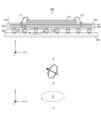
- FIG. 1A and 1B are a cross-sectional view and a diagram showing an example of a magnetic moment of a semiconductor device according to a first embodiment of the present technology
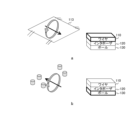
- FIG. 2 is a diagram showing an example of a magnetic moment according to the first embodiment of the present technology.
- 1 is a block diagram showing a configuration example of an information processing device according to a first embodiment of the present technology
- 3A to 3C are diagrams for explaining a method of analyzing a magnetic field distribution in the first embodiment of the present technology
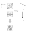
- 1A to 1C are diagrams illustrating an example of a magnetic field distribution and a magnetic moment before a design change in the first embodiment of the present technology.
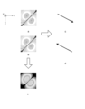
- 11A to 11C are diagrams illustrating an example of a magnetic field distribution and a magnetic moment after a design change in the first embodiment of the present technology.
- 1A to 1C are diagrams illustrating an example of a ball arrangement and a magnetic moment before and after a design change in the first embodiment of the present technology.
- 10A to 10C are diagrams for explaining a method for obtaining a minimum value of a magnetic field strength in the first embodiment of the present technology.
- 4 is a flowchart showing an example of an operation of the information processing device according to the first embodiment of the present technology.
- 4 is a diagram illustrating an example of a display screen of a magnetic field distribution in each layer according to the first embodiment of the present technology.
- 13 is an example of a display screen of a magnetic moment according to the first embodiment of the present technology.
- 13 is a diagram illustrating an example of a display screen of a combined magnetic field distribution according to the first embodiment of the present technology.
- 13A to 13C are diagrams for explaining a method of analyzing a magnetic field distribution in a modified example of the first embodiment of the present technology.
- 13A to 13C are diagrams illustrating an example of magnetic moments before and after synthesis in the second embodiment of the present technology.
- First embodiment example of determining the magnetic moment of each of two layers
- Second embodiment example of determining the magnetic moment of each of three layers
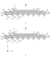
- First embodiment [Configuration example of semiconductor device] 1 is a diagram showing a cross-sectional view of a semiconductor device 100 according to a first embodiment of the present technology, and an example of a magnetic moment.
- a shows an example of a cross-sectional view of the semiconductor device 100.
- b shows a perspective view of the magnetic moment and loop current.
- c shows the magnetic moment and loop current when viewed from the side.
- the semiconductor device 100 includes a die 113, an interposer 123, and a mounting substrate 140.
- the die 113 is a chip on which various circuits are formed, and is electrically connected to the interposer 123 by a number of wires, such as wires 111 and 112.
- the surface to which the die 113 is connected is referred to as the "front surface" of the interposer 123.
- the interposer 123 electrically connects the die 113 and the mounting substrate 140. Wires and vias, such as a signal line 121, a power line (not shown), and a ground line 122, are formed within the interposer 123. In addition, a plurality of solder balls, such as solder balls 131 and 132, are arranged on the back surface of the interposer 123, and the interposer 123 is mounted to the mounting substrate 140 by these solder balls.
- the components consisting of the die 113, interposer 123, and mounting substrate 140 are called a semiconductor chip or a semiconductor package.
- the figure shows a specific semiconductor chip (or semiconductor package) among the various components arranged within the semiconductor device 100.
- the axis perpendicular to the substrate plane of the mounting substrate 140 is the "Z-axis", and a specific axis parallel to the substrate plane is the "X-axis”.
- the axis perpendicular to the X-axis and Z-axis is the "Y-axis”.
- "a" indicates a cross-sectional view seen from the Y-axis direction.
- solder ball 131 and wire 111 are connected to signal line 121.
- a signal current flows through wire 111, signal line 121, and solder ball 131.
- Solder ball 132 and wire 112 are connected to ground line 122.
- a return current flows through these when the circuit is driven.
- the arrow marked a in the figure indicates the direction of the current (signal current and return current).
- a magnetic field is generated by the loop current (signal current and return current) flowing through the loop-shaped path formed by the signal line 121 and ground line 122, and the strength and direction of the magnetic field are represented by the magnetic moment.
- the black arrow in b in the figure indicates the magnetic moment.
- c in the figure shows the magnetic moment and loop current viewed from the Y-axis direction when the magnetic moment is oriented in the Y-axis direction.
- the layer including the die 113 and wires is referred to as the conductor layer 110
- the layer including wiring and vias such as the signal line 121 and the ground line 122 in the interposer 123 is referred to as the conductor layer 120
- the layer in which multiple solder balls such as the solder balls 131 and 132 are arranged is referred to as the conductor layer 130.
- the semiconductor device 100 can be considered to include stacked conductor layers 110, 120, and 130. These conductor layers are electrically connected as described above.
- FIG. 2 is a diagram showing an example of magnetic moment in the first embodiment of the present technology.
- a is a perspective view showing the magnetic moment and loop current of the conductor layer 110 including the die 113 and the wire.
- b is a perspective view showing the magnetic moment and loop current of the conductor layer 130 including the solder ball.
- the direction of the magnetic moment in the magnetic field generated by conductor layer 110 is opposite to the direction of the magnetic moment in the magnetic field generated by conductor layer 130, and they cancel each other out.
- electromagnetic radiation from the semiconductor device 100 is mainly generated by current flowing through wires, vias, and solder balls.
- This electromagnetic radiation can be modeled by magnetic moment as described in IEC (International Electrotechnical Commission)_62433.
- IEC International Electrotechnical Commission
- Hr represents the magnetic field in the direction from the origin to the observation point P.
- I represents a loop-shaped current
- S represents the area of the loop through which the current flows.
- ⁇ represents the angle between the magnetic moment and the Z axis
- r represents the distance from the origin to the observation point P.
- f represents the frequency.
- Equation 3 shows that the strength of the magnetic field H increases as the distance r to the observation point decreases, and also increases as the current I increases. For this reason, the smaller r becomes due to high-density mounting, the greater the noise caused by the magnetic field. Furthermore, the greater the current I becomes due to more sophisticated devices, the greater the noise caused by the magnetic field.
- the magnetic moment in the magnetic field formed by conductor layer 110 and the magnetic moment in the magnetic field formed by conductor layer 130 cancel each other out.
- the strength of the magnetic field resulting from the combination of the magnetic field formed by conductor layer 110 and the magnetic field formed by conductor layer 130 becomes very small, and noise caused by this magnetic field can be sufficiently reduced.
- the semiconductor device 100 is designed so that the magnetic moment due to the loop current formed by the signal current and the return current cancels out, but is not limited to this configuration. It is also possible to design for the magnetic moment due to the loop current formed by the power supply current and the return current.
- the conductor layers 110 and 130 are designed so that their respective magnetic moments cancel each other out, but this is not limited to the configuration. It is also possible to design two layers other than the conductor layers 110 and 130 so that their magnetic moments cancel each other out.
- the conductor layer 110 is an example of a first conductor layer as described in the claims
- the conductor layer 130 is an example of a second conductor layer as described in the claims.
- FIG. 3 is a block diagram showing a configuration example of the information processing device 200 in the first embodiment of the present technology.
- the information processing device 200 includes a processing unit 205 and a display unit 250.
- the processing unit 205 includes a data holding unit 210, an electromagnetic field analysis unit 220, a magnetic moment acquisition unit 230, a magnetic field strength determination unit 240, and a design modification unit 260.
- a personal computer is assumed as the information processing device 200.
- the function of the processing unit 205 is realized by installing an application for circuit design in the information processing device 200.
- the information processing device 200 executes at least a part of the process of designing the semiconductor device 100 according to an operation signal from a user.
- the data storage unit 210 stores data for design. For example, design data for the semiconductor device 100 and data related to design constraints are stored in the data storage unit 210.
- the design data includes data indicating, for example, the arrangement of bonding pads, vias and solder balls on each of the conductor layers 110, 120, and 130, the circuit configuration, and the like.
- the electromagnetic field analysis unit 220 determines the magnetic field distribution of each of the multiple conductor layers (e.g., conductor layers 110 and 130) by electromagnetic field analysis based on the design data. This electromagnetic field analysis unit 220 displays the magnetic field distribution of each layer on the display unit 250. In addition, the electromagnetic field analysis unit 220 supplies the determined magnetic field distribution to the magnetic moment acquisition unit 230 and the magnetic field strength determination unit 240.
- the magnetic moment acquisition unit 230 determines the magnetic moment in the magnetic field of each of the multiple conductor layers based on the magnetic field distribution. This magnetic moment acquisition unit 230 displays the magnetic moment of each layer on the display unit 250.
- a method for determining the magnetic moment from the magnetic field distribution for example, the method described in "Yang Zhong, et.al., A New Reconstruction Method for a Source Above an Arbitrarily Shaped Ground Plane, IEEE 2020" can be used.
- the magnetic field strength determination unit 240 determines the strength of the magnetic field obtained by combining the magnetic fields of the multiple conductor layers, and determines whether the difference between the magnetic field strength and the minimum value under the design constraints is less than the allowable value (in other words, whether the magnetic field strength is approximately the minimum value). This magnetic field strength determination unit 240 displays the combined magnetic field distribution and the determination result on the display unit 250.
- the user refers to the information displayed on the display unit 250 and performs operations to change the design as necessary. For example, the user refers to the magnetic moments of each layer, and if they do not cancel each other out, attempts to change the design so that they cancel each other out.
- the design modification unit 260 modifies the design data in accordance with the user's operation signal. Note that although the user manually performs the design modifications, the information processing device 200 can also perform the design modifications automatically.
- FIG. 4 is a diagram for explaining a method for analyzing a magnetic field distribution in the first embodiment of the present technology.
- the information processing device 200 obtains the magnetic field distribution of an object of analysis in an analysis model in which a conductor layer that does not correspond to the object of analysis is surrounded by a perfect conductor.
- the conductor layer 110 is the subject of analysis.
- the information processing device 100 covers the periphery of the conductor layer 120 with a perfect conductor 151, and covers the periphery of the conductor layer 130 with a perfect conductor 152.
- the ground terminal (such as a pad) of the conductor layer 120 is connected to the perfect conductor 151, and the ground solder ball of the conductor layer 130 is connected to the perfect conductor 152.
- the electromagnetic field analysis unit 220 can analyze only the magnetic field distribution of the conductor layer 110 that is the subject of analysis.
- FIG. 5 shows an example of the magnetic field distribution and magnetic moment before the design change in the first embodiment of the present technology.
- a shows an example of the magnetic field distribution of the conductor layer 110
- b shows an example of the magnetic field distribution of the conductor layer 130.
- c shows an example of the magnetic moment obtained from the magnetic field distribution of a in the figure
- d shows an example of the magnetic moment obtained from the magnetic field distribution of b in the figure.
- e shows an example of the magnetic field distribution obtained by combining the magnetic field distributions of a and b in the figure.
- the magnetic moments of the conductor layers 110 and 130 have different orientations but do not cancel each other out.
- the combined magnetic field strength shown in e in the figure will be high, and the noise caused by this magnetic field will increase.
- the user can refer to the screen of the information processing device 200 to understand the orientation of the magnetic moments of each layer and make design changes so that the magnetic moments cancel each other out.
- FIG. 6 shows an example of the magnetic field distribution and magnetic moment after a design change in the first embodiment of the present technology.
- a shows an example of the magnetic moment and loop current of the conductor layer 110 after the design change
- b shows an example of the magnetic moment and loop current of the conductor layer 130 after the design change.
- c shows an example of the magnetic moment obtained from the magnetic field distribution of in the figure, a
- d shows an example of the magnetic moment obtained from the magnetic field distribution of in the figure, b.
- e shows an example of the magnetic field distribution obtained by combining the magnetic field distributions of in the figure, a and b.
- the magnetic moment of conductor layer 110 and the magnetic moment of conductor layer 130 are in the opposite directions and cancel each other out. This makes it possible to sufficiently reduce the combined magnetic field strength and reduce noise.
- FIG. 7 is a diagram showing an example of ball arrangement and magnetic moment before and after a design change in the first embodiment of the present technology.
- a is a perspective view showing an example of the magnetic moment and loop current of the conductor layer 130 before the design change.
- b is a plan view showing an example of the arrangement of solder balls on the conductor layer 130 before the design change.
- solder ball 131 which carries a signal current
- solder ball 132 which carries a return current.
- solder ball 132 is placed to the left of solder ball 131 when observed from the Z-axis direction. In this case, a magnetic moment is generated downward on the paper surface due to the loop current flowing through these solder balls.
- the user operates the information processing device 200 to make a design change to swap the positions of solder ball 131 and solder ball 132.
- C in the figure is a perspective view showing an example of the magnetic moment and loop current of the conductor layer 130 after the design change.
- d in the figure is a plan view showing an example of the arrangement of solder balls on the conductor layer 130 after the design change.
- the design change reverses the direction of the loop current and magnetic moment compared to before the design change.
- the direction of the magnetic moment can be changed by changing the arrangement of the solder balls.
- the direction of the magnetic moment can also be changed by changing the arrangement of the wires and vias, or by changing the circuit configuration.
- FIG. 8 is a diagram for explaining a method for determining the minimum value of the magnetic field strength in the first embodiment of the present technology.
- a is a plan view showing an example of the arrangement of solder balls before optimization.
- b is a graph showing an example of the variation in magnetic field strength due to a design change.
- c is a plan view showing an example of the arrangement of solder balls after optimization.
- Design parameters include the type, number and position of each of the solder balls, wires and vias.
- the type of current passing through may be either a signal current (or a signal current) or a return current.
- solder balls 131 through which a signal current flows and four solder balls 132 through which a return current flows is required on the conductor layer 130.
- Other conductor layers also have various design constraints for each design parameter regarding the type, number, and position of wires and vias. When making design changes, the user changes these design parameters under the design constraints.
- the magnetic field strength determination unit 240 in the information processing device 200 stores the set design parameters and the magnetic field strength after synthesis in correspondence with each other.
- the vertical axis of b in the figure indicates the magnetic field strength after synthesis, and the horizontal axis indicates the design parameters.
- the magnetic field strength determination unit 240 stores two or more plots on this graph, and uses curve fitting to find a curve function that best fits the group of plots.
- the magnetic field strength determination unit 240 finds the minimum value of the magnetic field strength under the constraint conditions as the global optimum solution based on that function.
- the magnetic field strength determination unit 240 determines whether the difference between the current magnetic field strength after synthesis and the found optimum solution (i.e., the minimum value) is less than a predetermined allowable value.
- the curve b in the figure indicates the curve obtained by curve fitting.
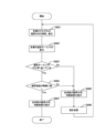
- Example of operation of information processing device 9 is a flowchart showing an example of the operation of the information processing device 200 according to the first embodiment of the present technology. This operation is started, for example, when a predetermined application for circuit design is executed.
- the information processing device 200 analyzes and displays the magnetic field distribution of each conductor layer (step S901). Then, the information processing device 200 converts the magnetic field distribution of each conductor layer into a magnetic moment and displays it (step S902). The user determines whether the magnetic moments of each layer cancel each other out (step S903). If the magnetic moments cancel each other out (step S903: Yes), the information processing device 200 determines whether the difference between the combined magnetic field strength and the minimum value under the design constraints is less than the allowable value (in other words, the magnetic field strength is approximately the minimum value) (step S904). The determination in step S903 can also be made by the information processing device 100 instead of the user.
- step S903 If the magnetic moments do not cancel each other out (step S903: No), or if the magnetic field strength is not at approximately the minimum value (step S904: No), the information processing device 200 displays the combined magnetic field distribution and the judgment result (step S905). Then, the information processing device 200 changes the design data according to the user's operation signal (step S906), and repeats steps S901 and onward.
- step S904 if the magnetic field strength is not approximately at the minimum value (step S904: Yes), the information processing device 200 displays the combined magnetic field distribution and the judgment result (step S907), and ends the operation for circuit design.
- the circuit is optimized by repeating steps S901 to S906.
- the information processing device 200 calculates and displays the magnetic moment for each conductor layer, allowing the user to efficiently design a semiconductor device 100 with reduced noise.
- a method including each of the steps illustrated in the figure is an example of a design method described in the claims.
- a program for causing a computer to execute the steps illustrated in the figure is an example of a program described in the claims.
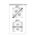
- FIG. 10 is an example of a display screen 500 showing the magnetic field distribution of each layer in the first embodiment of the present technology. As shown in the figure, the information processing device 200 determines and displays the magnetic field distribution of each of the conductor layer 110 and the conductor layer 130.
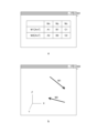
- FIG. 11 is an example of a display screen of the magnetic moment in the first embodiment of the present technology.
- the information processing device 200 determines and displays M1, which is the magnetic moment of the conductor layer 110, and M2, which is the magnetic moment of the conductor layer 130.
- the information processing device 200 decomposes each of the magnetic moments M1 and M2 into vectors Mx, My, and Mz in an orthogonal coordinate system of the X-axis, Y-axis, and Z-axis, and displays the vector quantities.
- the information processing device 200 displays each of the magnetic moments M1 and M2 as an arrow symbol in three-dimensional space.
- FIG. 12 is an example of a display screen 503 showing the combined magnetic field distribution in the first embodiment of the present technology. As shown in the figure, the information processing device 200 displays the combined magnetic field distribution of each conductor layer.
- Figs. 10 to 12 are examples of some of the screens displayed by the information processing device 200, and in addition to the above-mentioned screens, the information processing device 200 can display various screens for circuit design as necessary.
- the information processing device 200 displays the magnetic moment of each conductor layer, allowing the user to easily design a semiconductor device 100 with reduced noise.
- the information processing device 200 obtains the magnetic distribution of the analysis target by shielding the areas other than the analysis target, but is not limited to this analysis method.
- the information processing device 200 in this modified example of the first embodiment differs from the first embodiment in that an excitation source is connected to a conductor layer other than the analysis target.
- FIG. 13 is a diagram for explaining a method of analyzing a magnetic field distribution in a modified example of the first embodiment of the present technology.
- the information processing device 200 in the first modified example of the first embodiment obtains the magnetic field distribution of an object of analysis when an excitation source is connected to a terminal of a conductor layer that does not correspond to the object of analysis in an analysis model.
- the conductor layer 110 is the subject of analysis.
- the electromagnetic field analysis unit 220 performs calculations by dividing the structure of the subject of analysis into multiple mesh-like areas using an algorithm such as FDTD (Finite-Difference Time-Domain method).
- excitation sources such as V1, V2, V3, and V4 are connected to each of the terminals (solder balls 163, 164, and 165, pad 161, etc.) in the divided area.
- a voltage is applied as the excitation source. This allows the electromagnetic field analysis unit 220 to calculate the energy of all meshes and derive the magnetic field distribution of any surface.
- the electromagnetic field analysis unit 220 obtains the excitation source V1' at the boundary between the conductor layers 110 and 120 from the mesh energy information.
- the electromagnetic field analysis unit 220 connects an excitation source V1' to each of the terminals of the conductor layer that is not the subject of analysis.
- the excitation source V1' is connected to the terminals of the pad 162 of the conductor layer 120 and the solder balls 163, 164, and 165.
- the electromagnetic field analysis unit 220 can obtain only the magnetic field distribution of the conductor layer 110, excluding the electromagnetic radiation from the conductor layers 120 and 130.
- the electromagnetic field analysis unit 220 connects an excitation source to a terminal of a conductor layer that is not the subject of analysis, and therefore can obtain only the magnetic field distribution of the subject of analysis.
- FIG. 14 is a diagram showing an example of magnetic moments before and after synthesis in the second embodiment of the present technology.
- the electromagnetic field analysis unit 220 obtains the magnetic field distribution of the conductor layer 120 in addition to the magnetic field distribution of the conductor layers 110 and 130.
- the magnetic moment acquisition unit 230 then acquires the magnetic moments of the conductor layers 110, 120, and 130.
- the conductor layers 110, 120, and 130 are examples of the first, second, and third conductor layers described in the claims.
- a indicates the magnetic moment and loop current of the conductor layer 110
- b indicates the magnetic moment and loop current of the conductor layer 120
- c indicates the magnetic moment and loop current of the conductor layer 130.
- the magnetic moment acquisition unit 230 combines the magnetic moments of two of the three conductor layers. For example, the magnetic moments of conductor layers 120 and 130 are combined.
- d indicates the magnetic moment and loop current of the conductor layer 110
- e indicates the combined magnetic moment and loop current.
- the electromagnetic field analysis unit 220 causes the display unit 250 to display these magnetic moments. From this point on, the same processing as in the first embodiment is executed.
- the electromagnetic field analysis unit 220 can similarly combine and display multiple magnetic moments among them. Also, a modified version of the first embodiment can be applied to the second embodiment.
- the information processing device 200 synthesizes and displays the magnetic moments of two of the three layers, allowing the user to design efficiently.
- the present technology can also be configured as follows.
- An information processing device having a processing unit that performs processing to determine a first magnetic moment in a first magnetic field formed by a first conductor layer and a second magnetic moment in a second magnetic field formed by a second conductor layer stacked on the first conductor layer.
- the processing unit is an electromagnetic field analysis unit that determines distributions of the first and second magnetic fields from design data of the first and second conductor layers;
- the information processing device according to (1) further comprising: a magnetic moment acquisition unit that determines the first and second magnetic moments based on distributions of the first and second magnetic fields.
- the processing unit further includes a magnetic field strength determination unit that determines whether the difference between the magnetic field strength of the magnetic field obtained by combining the first and second magnetic fields and a predetermined minimum value is less than an allowable value.
- the electromagnetic field analysis unit determines the magnetic field distribution of the object to be analyzed when one of the first and second conductor layers that does not correspond to the object to be analyzed is shielded.
Landscapes
- Engineering & Computer Science (AREA)
- Computer Hardware Design (AREA)
- Physics & Mathematics (AREA)
- Theoretical Computer Science (AREA)
- Evolutionary Computation (AREA)
- Geometry (AREA)
- General Engineering & Computer Science (AREA)
- General Physics & Mathematics (AREA)
- Shielding Devices Or Components To Electric Or Magnetic Fields (AREA)
Abstract
Description
1.第1の実施の形態(2層のそれぞれの磁気モーメントを求める例)
2.第2の実施の形態(3層のそれぞれの磁気モーメントを求める例)
[半導体装置の構成例]
図1は、本技術の第1の実施の形態における半導体装置100の断面図、および、磁気モーメントの一例を示す図である。同図におけるaは、半導体装置100の断面図の一例を示す。同図におけるbは、磁気モーメントおよびループ電流の斜視図を示す。同図におけるcは、側面から見た際の磁気モーメントおよびループ電流を示す。


H=(I×f2×S)/r ・・・式3
図3は、本技術の第1の実施の形態における情報処理装置200の一構成例を示すブロック図である。この情報処理装置200は、処理部205および表示部250を備える。処理部205は、データ保持部210、電磁界解析部220、磁気モーメント取得部230、磁界強度判定部240および設計変更部260を備える。情報処理装置200として、例えば、パーソナルコンピュータが想定される。処理部205の機能は、例えば、情報処理装置200に、回路設計用のアプリケーションをインストールすることにより実現される。情報処理装置200は、ユーザの操作信号に従って、半導体装置100を設計する工程の少なくとも一部を実行する。
図9は、本技術の第1の実施の形態における情報処理装置200の動作の一例を示すフローチャートである。この動作は、例えば、回路設計のための所定のアプリケーションが実行されたときに開始される。
上述の第1の実施の形態では、情報処理装置200は、解析対象以外をシールドすることにより、解析対象の磁気分布を求めていたが、この解析方法に限定されない。この第1の実施の形態の変形例における情報処理装置200は、解析対象以外の導体層に励振源を接続する点において第1の実施の形態と異なる。
上述の第1の実施の形態では、導体層110や130などの2層のそれぞれの磁気モーメントを求めていたが、3層以上の導体層のそれぞれの磁気モーメントを求めることもできる。
(1)第1の導体層が形成する第1の磁界内の第1の磁気モーメントと前記第1の導体層に積層される第2の導体層が形成する第2の磁界内の第2の磁気モーメントとを求める処理を行う処理部を具備する情報処理装置。
(2)前記処理部は、
前記第1および第2の導体層のそれぞれの設計データから前記第1および第2の磁界の分布を求める電磁界解析部と、
前記第1および第2の磁界の分布に基づいて前記第1および第2の磁気モーメントを求める磁気モーメント取得部と
を備える前記(1)記載の情報処理装置。
(3)前記処理部は、前記設計データを変更する設計変更部をさらに備える
前記(2)記載の情報処理装置。
(4)前記処理部は、前記第1および第2の磁界を合成した磁界の磁界強度と所定の最小値との差が許容値未満か否かを判定する磁界強度判定部をさらに備える
前記(2)または(3)に記載の情報処理装置。
(5)前記電磁界解析部は、前記第1および第2の導体層のうち解析対象に該当しない方の導体層をシールドした場合の前記解析対象の磁界分布を求める
前記(2)から(4)のいずれかに記載の情報処理装置。
(6)前記電磁界解析部は、前記第1および第2の導体層のうち解析対象に該当しない方の導体層の端子に所定の励振源を接続した場合の前記解析対象の磁界分布を求める
前記(2)から(4)のいずれかに記載の情報処理装置。
(7)前記磁気モーメント取得部は、第2の導体層に積層される第3の導体層が形成する第3の磁気モーメントと前記第1、第2および第3の磁気モーメントのうち2つを合成した磁気モーメントとをさらに求める
前記(2)から(6)のいずれかに記載の情報処理装置。
(8)前記処理部は、前記第1および第2の磁気モーメントのそれぞれを表示部に表示させる
前記(1)から(7)のいずれかに記載の情報処理装置。
(9)情報処理装置が、第1の導体層が形成する第1の磁界内の第1の磁気モーメントと前記第1の導体層に積層される第2の導体層が形成する第2の磁界分内の第2の磁気モーメントとを求める手順を具備する半導体装置の設計方法。
(10)情報処理装置が、第1の導体層が形成する第1の磁界内の第1の磁気モーメントと前記第1の導体層に積層される第2の導体層が形成する第2の磁界分内の第2の磁気モーメントとを求める手順をコンピュータに実行させるためのプログラム。
(11)第1の磁気モーメントを有する第1の磁界を形成する第1の導体層と、
前記第1の導体層に積層され、前記第1の磁気モーメントとの間で打ち消しあう第2の磁気モーメントを有する第2の磁界を形成する第2の導体層と
を具備する半導体装置。
110、120、130 導体層
111、112 ワイヤ
113 ダイ
121 信号線
122 グランド線
123 インターポーザ
131、132、163~165 ソルダーボール
140 実装基板
151、152 完全導体
161、162 パッド
200 情報処理装置
205 処理部
210 データ保持部
220 電磁界解析部
230 磁気モーメント取得部
240 磁界強度判定部
250 表示部
260 設計変更部
Claims (11)
- 第1の導体層が形成する第1の磁界内の第1の磁気モーメントと前記第1の導体層に積層される第2の導体層が形成する第2の磁界内の第2の磁気モーメントとを求める処理を行う処理部を具備する情報処理装置。
- 前記処理部は、
前記第1および第2の導体層のそれぞれの設計データから前記第1および第2の磁界の分布を求める電磁界解析部と、
前記第1および第2の磁界の分布に基づいて前記第1および第2の磁気モーメントを求める磁気モーメント取得部と
を備える請求項1記載の情報処理装置。 - 前記処理部は、前記設計データを変更する設計変更部をさらに備える
請求項2記載の情報処理装置。 - 前記処理部は、前記第1および第2の磁界を合成した磁界の磁界強度と所定の最小値との差が許容値未満か否かを判定する磁界強度判定部をさらに備える
請求項2記載の情報処理装置。 - 前記電磁界解析部は、前記第1および第2の導体層のうち解析対象に該当しない方の導体層をシールドした場合の前記解析対象の磁界分布を求める
請求項2記載の情報処理装置。 - 前記電磁界解析部は、前記第1および第2の導体層のうち解析対象に該当しない方の導体層の端子に所定の励振源を接続した場合の前記解析対象の磁界分布を求める
請求項2記載の情報処理装置。 - 前記磁気モーメント取得部は、第2の導体層に積層される第3の導体層が形成する第3の磁気モーメントと前記第1、第2および第3の磁気モーメントのうち2つを合成した磁気モーメントとをさらに求める
請求項2記載の情報処理装置。 - 前記処理部は、前記第1および第2の磁気モーメントのそれぞれを表示部に表示させる
請求項1記載の情報処理装置。 - 情報処理装置が、第1の導体層が形成する第1の磁界内の第1の磁気モーメントと前記第1の導体層に積層される第2の導体層が形成する第2の磁界分内の第2の磁気モーメントとを求める手順を具備する半導体装置の設計方法。
- 情報処理装置が、第1の導体層が形成する第1の磁界内の第1の磁気モーメントと前記第1の導体層に積層される第2の導体層が形成する第2の磁界分内の第2の磁気モーメントとを求める手順をコンピュータに実行させるためのプログラム。
- 第1の磁気モーメントを有する第1の磁界を形成する第1の導体層と、
前記第1の導体層に積層され、前記第1の磁気モーメントとの間で打ち消しあう第2の磁気モーメントを有する第2の磁界を形成する第2の導体層と
を具備する半導体装置。
Priority Applications (2)
| Application Number | Priority Date | Filing Date | Title |
|---|---|---|---|
| EP24831409.8A EP4733977A1 (en) | 2023-06-26 | 2024-05-07 | Information processing device, design method, program, and semiconductor device |
| JP2025529479A JPWO2025004536A1 (ja) | 2023-06-26 | 2024-05-07 |
Applications Claiming Priority (2)
| Application Number | Priority Date | Filing Date | Title |
|---|---|---|---|
| JP2023-104421 | 2023-06-26 | ||
| JP2023104421 | 2023-06-26 |
Publications (1)
| Publication Number | Publication Date |
|---|---|
| WO2025004536A1 true WO2025004536A1 (ja) | 2025-01-02 |
Family
ID=93938227
Family Applications (1)
| Application Number | Title | Priority Date | Filing Date |
|---|---|---|---|
| PCT/JP2024/016983 Ceased WO2025004536A1 (ja) | 2023-06-26 | 2024-05-07 | 情報処理装置、設計方法、プログラム、および、半導体装置 |
Country Status (3)
| Country | Link |
|---|---|
| EP (1) | EP4733977A1 (ja) |
| JP (1) | JPWO2025004536A1 (ja) |
| WO (1) | WO2025004536A1 (ja) |
Citations (4)
| Publication number | Priority date | Publication date | Assignee | Title |
|---|---|---|---|---|
| JPH09167851A (ja) * | 1995-12-14 | 1997-06-24 | Nec Corp | 太陽電池電源装置 |
| JP2002202332A (ja) * | 2000-12-27 | 2002-07-19 | Matsushita Electric Works Ltd | 照明器具からの放射ノイズ空間分布予測システム、そのプログラム、そのプログラムを記録した媒体 |
| JP2014082393A (ja) | 2012-10-18 | 2014-05-08 | Canon Inc | プリント回路板 |
| JP2016177189A (ja) * | 2015-03-20 | 2016-10-06 | 株式会社ジャパンディスプレイ | 表示装置 |
-
2024
- 2024-05-07 JP JP2025529479A patent/JPWO2025004536A1/ja active Pending
- 2024-05-07 WO PCT/JP2024/016983 patent/WO2025004536A1/ja not_active Ceased
- 2024-05-07 EP EP24831409.8A patent/EP4733977A1/en active Pending
Patent Citations (4)
| Publication number | Priority date | Publication date | Assignee | Title |
|---|---|---|---|---|
| JPH09167851A (ja) * | 1995-12-14 | 1997-06-24 | Nec Corp | 太陽電池電源装置 |
| JP2002202332A (ja) * | 2000-12-27 | 2002-07-19 | Matsushita Electric Works Ltd | 照明器具からの放射ノイズ空間分布予測システム、そのプログラム、そのプログラムを記録した媒体 |
| JP2014082393A (ja) | 2012-10-18 | 2014-05-08 | Canon Inc | プリント回路板 |
| JP2016177189A (ja) * | 2015-03-20 | 2016-10-06 | 株式会社ジャパンディスプレイ | 表示装置 |
Non-Patent Citations (2)
| Title |
|---|
| See also references of EP4733977A1 |
| YANG ZHONG: "A New Reconstruction Method for a Source Above an Arbitrarily Shaped Ground Plane", 2020, IEEE |
Also Published As
| Publication number | Publication date |
|---|---|
| EP4733977A1 (en) | 2026-04-29 |
| JPWO2025004536A1 (ja) | 2025-01-02 |
Similar Documents
| Publication | Publication Date | Title |
|---|---|---|
| US11506730B2 (en) | Magnetic field measurement systems including a plurality of wearable sensor units having a magnetic field generator | |
| US6598208B2 (en) | Design and assisting system and method using electromagnetic position | |
| JP5108322B2 (ja) | 撮像システムにおいて受信器コイルと一体化した回路に対する自己遮蔽式パッケージ実装 | |
| JP4597691B2 (ja) | 有限要素法を用いた構造解析方法 | |
| US20110167399A1 (en) | Design tool for the type and form of a circuit production | |
| CN103515267A (zh) | 布线数据的生成装置、生成方法及描画装置 | |
| Kim et al. | High-efficiency PCB-and package-level wireless power transfer interconnection scheme using magnetic field resonance coupling | |
| JP3189801B2 (ja) | 半導体評価装置,これに用いる磁界検出器及びこの製造方法並びに半導体評価用プログラムを記憶した記憶媒体 | |
| US20060279306A1 (en) | Test equipment of semiconductor devices | |
| Wu et al. | Characteristic mode analysis of radiating structures in digital systems | |
| JP2007041867A (ja) | インダクタンス解析システムと方法並びにプログラム | |
| WO2025004536A1 (ja) | 情報処理装置、設計方法、プログラム、および、半導体装置 | |
| JP2003086721A (ja) | 半導体装置および半導体装置を用いた電子装置の設計支援方法 | |
| JP4528024B2 (ja) | 回路解析方法を実行させるためのプログラム | |
| US20080244480A1 (en) | System and method to generate an IC layout using simplified manufacturing rule | |
| JP2009251856A (ja) | 設計支援装置 | |
| US20100095257A1 (en) | Electromagnetic field analysis of semiconductor package with semiconductor chip mounted thereon | |
| US20170372989A1 (en) | Exposed side-wall and lga assembly | |
| CN120359611A (zh) | 用于半导体设计和制造的可重复使用的模板 | |
| Tago et al. | Reducing EMI in wire-bond BGA IC-chips through magnetic dipole moment control | |
| JP2001320137A (ja) | 電子装置搭載機器 | |
| JP2004020403A (ja) | 電子機器表示装置、電子機器、及びその製造方法 | |
| JP2012244082A (ja) | 露光データの生成方法 | |
| JPWO2015133052A1 (ja) | 情報処理装置、情報処理方法および情報処理プログラムが記憶された記憶媒体 | |
| JP4086870B2 (ja) | プリント回路基板設計支援装置、方法およびプログラム |
Legal Events
| Date | Code | Title | Description |
|---|---|---|---|
| 121 | Ep: the epo has been informed by wipo that ep was designated in this application |
Ref document number: 24831409 Country of ref document: EP Kind code of ref document: A1 |
|
| ENP | Entry into the national phase |
Ref document number: 2025529479 Country of ref document: JP Kind code of ref document: A |
|
| WWE | Wipo information: entry into national phase |
Ref document number: 2025529479 Country of ref document: JP |
|
| ENP | Entry into the national phase |
Ref document number: 2024831409 Country of ref document: EP Effective date: 20260126 |
|
| WWE | Wipo information: entry into national phase |
Ref document number: 2024831409 Country of ref document: EP |
|
| NENP | Non-entry into the national phase |
Ref country code: DE |
|
| ENP | Entry into the national phase |
Ref document number: 2024831409 Country of ref document: EP Effective date: 20260126 |
|
| ENP | Entry into the national phase |
Ref document number: 2024831409 Country of ref document: EP Effective date: 20260126 |