WO2025004486A1 - 積層セラミックコンデンサ - Google Patents
積層セラミックコンデンサ Download PDFInfo
- Publication number
- WO2025004486A1 WO2025004486A1 PCT/JP2024/013795 JP2024013795W WO2025004486A1 WO 2025004486 A1 WO2025004486 A1 WO 2025004486A1 JP 2024013795 W JP2024013795 W JP 2024013795W WO 2025004486 A1 WO2025004486 A1 WO 2025004486A1
- Authority
- WO
- WIPO (PCT)
- Prior art keywords
- layer
- electrode
- region
- laminate
- multilayer ceramic
- Prior art date
- Legal status (The legal status is an assumption and is not a legal conclusion. Google has not performed a legal analysis and makes no representation as to the accuracy of the status listed.)
- Ceased
Links
Images




Classifications
-
- H—ELECTRICITY
- H01—ELECTRIC ELEMENTS
- H01G—CAPACITORS; CAPACITORS, RECTIFIERS, DETECTORS, SWITCHING DEVICES, LIGHT-SENSITIVE OR TEMPERATURE-SENSITIVE DEVICES OF THE ELECTROLYTIC TYPE
- H01G4/00—Fixed capacitors; Processes of their manufacture
- H01G4/30—Stacked capacitors
-
- H—ELECTRICITY
- H01—ELECTRIC ELEMENTS
- H01G—CAPACITORS; CAPACITORS, RECTIFIERS, DETECTORS, SWITCHING DEVICES, LIGHT-SENSITIVE OR TEMPERATURE-SENSITIVE DEVICES OF THE ELECTROLYTIC TYPE
- H01G4/00—Fixed capacitors; Processes of their manufacture
- H01G4/002—Details
- H01G4/005—Electrodes
- H01G4/008—Selection of materials
-
- H—ELECTRICITY
- H01—ELECTRIC ELEMENTS
- H01G—CAPACITORS; CAPACITORS, RECTIFIERS, DETECTORS, SWITCHING DEVICES, LIGHT-SENSITIVE OR TEMPERATURE-SENSITIVE DEVICES OF THE ELECTROLYTIC TYPE
- H01G4/00—Fixed capacitors; Processes of their manufacture
- H01G4/002—Details
- H01G4/005—Electrodes
- H01G4/012—Form of non-self-supporting electrodes
-
- H—ELECTRICITY
- H01—ELECTRIC ELEMENTS
- H01G—CAPACITORS; CAPACITORS, RECTIFIERS, DETECTORS, SWITCHING DEVICES, LIGHT-SENSITIVE OR TEMPERATURE-SENSITIVE DEVICES OF THE ELECTROLYTIC TYPE
- H01G4/00—Fixed capacitors; Processes of their manufacture
- H01G4/002—Details
- H01G4/018—Dielectrics
- H01G4/06—Solid dielectrics
- H01G4/08—Inorganic dielectrics
- H01G4/12—Ceramic dielectrics
-
- H—ELECTRICITY
- H01—ELECTRIC ELEMENTS
- H01G—CAPACITORS; CAPACITORS, RECTIFIERS, DETECTORS, SWITCHING DEVICES, LIGHT-SENSITIVE OR TEMPERATURE-SENSITIVE DEVICES OF THE ELECTROLYTIC TYPE
- H01G4/00—Fixed capacitors; Processes of their manufacture
- H01G4/002—Details
- H01G4/018—Dielectrics
- H01G4/06—Solid dielectrics
- H01G4/08—Inorganic dielectrics
- H01G4/12—Ceramic dielectrics
- H01G4/1209—Ceramic dielectrics characterised by the ceramic dielectric material
-
- H—ELECTRICITY
- H01—ELECTRIC ELEMENTS
- H01G—CAPACITORS; CAPACITORS, RECTIFIERS, DETECTORS, SWITCHING DEVICES, LIGHT-SENSITIVE OR TEMPERATURE-SENSITIVE DEVICES OF THE ELECTROLYTIC TYPE
- H01G4/00—Fixed capacitors; Processes of their manufacture
- H01G4/002—Details
- H01G4/018—Dielectrics
- H01G4/06—Solid dielectrics
- H01G4/08—Inorganic dielectrics
- H01G4/12—Ceramic dielectrics
- H01G4/1209—Ceramic dielectrics characterised by the ceramic dielectric material
- H01G4/1218—Ceramic dielectrics characterised by the ceramic dielectric material based on titanium oxides or titanates
-
- H—ELECTRICITY
- H01—ELECTRIC ELEMENTS
- H01G—CAPACITORS; CAPACITORS, RECTIFIERS, DETECTORS, SWITCHING DEVICES, LIGHT-SENSITIVE OR TEMPERATURE-SENSITIVE DEVICES OF THE ELECTROLYTIC TYPE
- H01G4/00—Fixed capacitors; Processes of their manufacture
- H01G4/002—Details
- H01G4/018—Dielectrics
- H01G4/06—Solid dielectrics
- H01G4/08—Inorganic dielectrics
- H01G4/12—Ceramic dielectrics
- H01G4/1209—Ceramic dielectrics characterised by the ceramic dielectric material
- H01G4/1218—Ceramic dielectrics characterised by the ceramic dielectric material based on titanium oxides or titanates
- H01G4/1227—Ceramic dielectrics characterised by the ceramic dielectric material based on titanium oxides or titanates based on alkaline earth titanates
-
- H—ELECTRICITY
- H01—ELECTRIC ELEMENTS
- H01G—CAPACITORS; CAPACITORS, RECTIFIERS, DETECTORS, SWITCHING DEVICES, LIGHT-SENSITIVE OR TEMPERATURE-SENSITIVE DEVICES OF THE ELECTROLYTIC TYPE
- H01G4/00—Fixed capacitors; Processes of their manufacture
- H01G4/002—Details
- H01G4/228—Terminals
- H01G4/232—Terminals electrically connecting two or more layers of a stacked or rolled capacitor
-
- H—ELECTRICITY
- H01—ELECTRIC ELEMENTS
- H01G—CAPACITORS; CAPACITORS, RECTIFIERS, DETECTORS, SWITCHING DEVICES, LIGHT-SENSITIVE OR TEMPERATURE-SENSITIVE DEVICES OF THE ELECTROLYTIC TYPE
- H01G4/00—Fixed capacitors; Processes of their manufacture
- H01G4/002—Details
- H01G4/228—Terminals
- H01G4/232—Terminals electrically connecting two or more layers of a stacked or rolled capacitor
- H01G4/2325—Terminals electrically connecting two or more layers of a stacked or rolled capacitor characterised by the material of the terminals
-
- H—ELECTRICITY
- H01—ELECTRIC ELEMENTS
- H01G—CAPACITORS; CAPACITORS, RECTIFIERS, DETECTORS, SWITCHING DEVICES, LIGHT-SENSITIVE OR TEMPERATURE-SENSITIVE DEVICES OF THE ELECTROLYTIC TYPE
- H01G4/00—Fixed capacitors; Processes of their manufacture
- H01G4/35—Feed-through capacitors or anti-noise capacitors
Definitions
- This invention relates to multilayer ceramic capacitors.
- multilayer ceramic capacitors such as the three-terminal feed-through capacitor shown in Patent Document 1 have excellent low impedance characteristics in the high frequency band, and by increasing the number of multilayer ceramic capacitors (the number connected in parallel), it becomes possible to design low impedance circuits.
- the impedance characteristics of a three-terminal feed-through capacitor tend to show low impedance when the current path through the second region extending from the second internal electrode to the fifth and sixth surfaces becomes shorter.
- the current path flows closer to the edge of the internal electrode, and if the linearity of the edge of the internal electrode deteriorates due to overfiring, for example, the current path becomes longer, which may result in high impedance.
- the main objective of this invention is to provide a multilayer ceramic capacitor that can further improve low impedance characteristics.
- the multilayer ceramic capacitor of the present invention comprises a laminate having a first surface and a second surface that face each other in a lamination direction, a third surface and a fourth surface that face each other in a first direction perpendicular to the lamination direction, and a fifth surface and a sixth surface that face each other in a second direction perpendicular to the lamination direction and the first direction, a first external electrode arranged on the third surface of the laminate, a second external electrode arranged on the fourth surface of the laminate, a third external electrode arranged on the fifth surface of the laminate, and a fourth external electrode arranged on the sixth surface of the laminate, the laminate having an inner layer portion and
- the multilayer ceramic capacitor has two outer layers arranged so as to sandwich the two outer layers in the stacking direction, the inner layer has an inner dielectric layer, a first inner electrode having one end in a first direction exposed on the third and fourth faces, and a second inner electrode having one end in a second direction exposed on the fifth and sixth faces, the second inner electrode has a first region
- the second internal electrode comprises a first region disposed inside the laminate and a second region extending from the first region to the fifth and sixth surfaces, and a convex portion is disposed on at least one of the edge portions of the second region that face each other in the first direction.
- This invention provides a multilayer ceramic capacitor that can further improve low impedance characteristics.
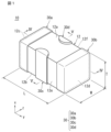
- FIG. 1 is an external perspective view showing a multilayer ceramic capacitor according to the present invention
- 1 is a front view showing a multilayer ceramic capacitor according to the present invention
- 1 is a top view showing a multilayer ceramic capacitor according to the present invention.
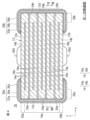
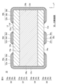
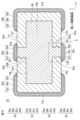
- FIG. 4 is a cross-sectional view taken along line IV-IV in FIG. 2 is a cross-sectional view taken along line VV in FIG. 1.
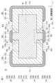
- 6 is a cross-sectional view taken along line VI-VI in FIG. 4.
- FIG. 7 is a cross-sectional view taken along line VII-VII in FIG.
- FIG. 8 is an enlarged view of part A in FIG. 7 .
- FIG. 11 is a cross-sectional view showing a modified example of the second internal electrode.
- FIG. 1 is an external perspective view of a multilayer ceramic capacitor according to the present invention.
- Fig. 2 is a front view of a multilayer ceramic capacitor according to the present invention.
- Fig. 3 is a top view of a multilayer ceramic capacitor according to the present invention.
- Fig. 4 is a cross-sectional view taken along line IV-IV in Fig. 1.
- Fig. 5 is a cross-sectional view taken along line V-V in Fig. 1.
- Fig. 6 is a cross-sectional view taken along line VI-VI in Fig. 4.
- Fig. 7 is a cross-sectional view taken along line VII-VII in Fig. 4.
- Fig. 8 is an enlarged view of part A in Fig. 7.
- the multilayer ceramic capacitor 10 comprises a laminate 12 and a plurality of external electrodes 30.
- the laminate 12 has a first surface 12a and a second surface 12b that face the stacking direction x, a third surface 12c and a fourth surface 12d that face the first direction y that is perpendicular to the stacking direction x, and a fifth surface 12e and a sixth surface 12f that face the second direction z that is perpendicular to the stacking direction x and the first direction y.
- the direction that connects the first surface 12a and the second surface 12b of the laminate 12 is the stacking direction x.
- the laminate 12 has a rectangular parallelepiped shape. It is preferable that the corners and ridges of the laminate 12 are rounded. The corners are the parts where three adjacent faces of the laminate 12 intersect, and the ridges are the parts where two adjacent faces of the laminate 12 intersect. In addition, unevenness may be formed on some or all of the first face 12a and the second face 12b, the third face 12c and the fourth face 12d, and the fifth face 12e and the sixth face 12f.
- the laminate 12 has a plurality of dielectric layers 14 and a plurality of internal electrodes 16.
- the dielectric layers 14 include an inner dielectric layer 14a and an outer dielectric layer 14b.
- the internal electrodes 16 have a first internal electrode 16a and a second internal electrode 16b.
- the laminate 12 also has an inner layer portion 18, a first main surface side outer layer portion 20a located on the first surface 12a side, and a second main surface side outer layer portion 20b located on the second surface 12b side.
- the first main surface outer layer portion 20a is located on the first surface 12a side of the laminate 12, and is an assembly of multiple outer dielectric layers 14b located between the first surface 12a and the internal electrode 16 closest to the first surface 12a.
- the second main surface side outer layer portion 20b is located on the second surface 12b side of the laminate 12, and is an assembly of multiple outer dielectric layers 14b located between the second surface 12b and the internal electrode 16 closest to the second surface 12b.
- the area sandwiched between the first main surface side outer layer portion 20a and the second main surface side outer layer portion 20b is the inner layer portion 18.
- the inner layer portion 18 has a first inner electrode 16a, one end of which is exposed on the third surface 12c and the other end of which is exposed on the fourth surface 12d, a second inner electrode 16b, one end of which is exposed on the fifth surface 12e and the other end of which is exposed on the sixth surface 12f, and an inner dielectric layer 14a.
- the dielectric layer 14 may be formed of, for example, a dielectric material.
- a dielectric ceramic composed of a main component such as BaTiO3 , CaTiO3 , SrTiO3 , or CaZrO3 may be used as the dielectric material.
- a subcomponent such as a Mn compound, an Fe compound, a Cr compound, a Co compound, or a Ni compound may be added to the main component.
- the inner dielectric layer 14a and the outer dielectric layer 14b may be composed of the same dielectric material or different dielectric materials.
- the inner dielectric layer 14a contains a large amount of CaTiO3 or CaZrO3 as a dielectric component, it is possible to make it difficult for insulation breakdown to occur between the first inner electrode 16a and the second inner electrode 16b.
- the inner dielectric layer 14a may be mainly composed of SrTiO3 or the like.
- the inner dielectric layer 14a is formed of a material with a high dielectric constant, for example, BaTiO3 .
- the number of dielectric layers 14 to be stacked is not particularly limited, but is preferably 5 to 1000, including the first main surface side outer layer 20a and the second main surface side outer layer 20b.
- the thickness of the dielectric layer 14 is preferably, for example, 0.3 ⁇ m to 6.0 ⁇ m.
- the internal electrode 16 includes a first internal electrode 16a and a second internal electrode 16b.
- the first internal electrode 16a is disposed on the surface of the inner dielectric layer 14a.
- the first internal electrode 16a has a first opposing electrode portion 22a located inside the laminate 12, a first extraction electrode portion 24a connected to the first opposing electrode portion 22a and extracted to the third surface 12c, and a second extraction electrode portion 24b extracted to the fourth surface 12d.
- the shape of the first opposing electrode portion 22a of the first internal electrode 16a is not particularly limited, but is preferably rectangular in plan view. However, the corners in plan view may be rounded or may be formed at an angle in plan view (tapered). It may also be tapered in plan view, with an incline in either direction.
- the shapes of the first and second extraction electrode portions 24a and 24b of the first internal electrode 16a are not particularly limited, but are preferably rectangular in plan view. However, the corners in plan view may be rounded or may be formed at an angle in plan view (tapered). They may also be tapered in plan view, with an incline toward either side.
- the second internal electrode 16b is disposed on a surface of an inner dielectric layer 14a different from the inner dielectric layer 14a on which the first internal electrode 16a is disposed.
- the second internal electrode 16b has a second opposing electrode portion 22b that faces the first internal electrode 16a, a third extraction electrode portion 24c that is connected to the second opposing electrode portion 22b and is extended to the fifth surface 12e, and a fourth extraction electrode portion 24d that is extended to the sixth surface 12f.
- the shape of the second opposing electrode portion 22b of the second internal electrode 16b is not particularly limited, but is preferably rectangular in plan view. However, the corners in plan view may be rounded or may be formed at an angle in plan view (tapered). It may also be tapered in plan view, with an incline in either direction.
- the shapes of the third extraction electrode portion 24c and the fourth extraction electrode portion 24d of the second internal electrode 16b are not particularly limited, but are preferably rectangular in plan view. However, the corners in plan view may be rounded or may be formed at an angle in plan view (tapered). Also, they may be tapered in plan view with an incline toward either side.
- the second opposing electrode portion 22b of the second internal electrode 16b is the first region 40, and the third extraction electrode portion 24c and the fourth extraction electrode portion 24d of the second internal electrode 16b are the second region 42.
- the first region 40 of the second internal electrode 16b is a region that is disposed inside the laminate 12.
- the second region 42 of the second internal electrode 16b is a region that is extracted from the first region 40 to the fifth surface 12e and the sixth surface 12f.
- a first convex portion 50a protruding in the direction connecting the third surface 12c and the fourth surface 12d (first direction y) is arranged on both end edges 42a located opposite the first direction y of the second region 42.
- a second convex portion 50b protruding in the direction connecting the third surface 12c and the fourth surface 12d (first direction y) is arranged on both end edges 42b located opposite the first direction y of the second region 42.
- the inside of the first convex portion 40a and the second convex portion 40b form a current path, the current path from the first region 40 via the second region 42 to the external electrode 30 can be shortened. As a result, the ESL (equivalent series inductance) of the multilayer ceramic capacitor 10 can be reduced, and low impedance characteristics can be achieved.
- the length L1 in the first direction y at the boundary between the first region 40 and the second region 42, and the maximum length L2 in the first direction y of the edge portion 42a of the first protrusion 50a can be measured, for example, by the following method.
- the laminated ceramic capacitor 10 is polished to 1/2 of the length in the stacking direction x.
- the polished cross section is observed, for example, using a digital microscope to view the first region 40 and the second region 42.
- the length in the first direction y at the observed boundary between the first region 40 and the second region 42 is measured to obtain L1
- the maximum length in the first direction y of the edge portion 42a of the first protrusion 50a is measured to obtain L2.
- this is not limited to this, and the cross section exposed by polishing to 1/4 or 3/4 of the length in the stacking direction x of the laminated ceramic capacitor 10 may be used for measurement.
- the intersection between the first region 40 and the second region 42 may not be a right angle.
- the length L1 is determined based on the straight line portion along the first direction y at the edge of the first region 40.
- the length W1 in the second direction z of the second region 42 and the length W2 in the second direction z of the edge portion 42b of the first protrusion 50a can be measured, for example, by the following method.
- the multilayer ceramic capacitor 10 is polished to 1/2 of the length in the stacking direction x.
- the first region 40 and the second region 42 are observed on the polished cross section, for example, using a digital microscope.
- the length in the second direction z of the observed second region 42 is measured to obtain W1
- the length in the second direction z of the edge portion 42b of the first protrusion 50a is measured to obtain W2.
- this is not limited to this, and the cross section exposed by polishing to 1/4 or 3/4 of the length in the stacking direction x of the multilayer ceramic capacitor 10 may be used for measurement.
- the intersection between the first region 40 and the second region 42 may not be a right angle.
- the length W1 is determined based on the straight line portion along the edge of the second region 42.
- the first convex portion 50a may be disposed on at least one of the edge portions 42a located opposite to each other in the first direction y of the second region 42 on the fifth surface 12e side of the second internal electrode 16b.
- the second convex portion 50b may be disposed on at least one of the edge portions 42b located opposite to each other in the first direction y of the second region 42 on the sixth surface 12f side of the second internal electrode 16b.
- the insides of the first convex portion 40a and the second convex portion 40b become a current path, so that the current path from the first region 40 to the external electrode 30 via the second region 42 can be shortened, and as a result, the ESL of the multilayer ceramic capacitor 10 can be reduced, and low impedance characteristics can be realized.
- the first internal electrode 16a and the second internal electrode 16b can be made of an appropriate conductive material, such as metals such as Ni, Cu, Ag, Pd, and Au, or alloys containing at least one of these metals, such as Ni-Cu alloys and Ag-Pd alloys, but are not limited to these. Furthermore, the first internal electrode 16a and the second internal electrode 16b may be made of the same conductive material or different conductive materials.
- the electric field concentration at the interface between the internal electrode 16 and the dielectric layer 14 can be alleviated, leading to improved high temperature load reliability.
- Sn is included in only one of the internal electrodes 16, either the first internal electrode 16a or the second internal electrode 16b, it can be sufficiently effective.
- the total number of the first internal electrodes 16a and the second internal electrodes 16b is 2 or more and 1000 or less.
- the thickness of the first internal electrodes 16a and the second internal electrodes 16b is not particularly limited, but is preferably, for example, 0.3 ⁇ m or more and 6.0 ⁇ m or less.
- the first opposing electrode portion 22a of the first internal electrode 16a and the second opposing electrode portion 22b of the second internal electrode 16b face each other via the inner dielectric layer 14a, forming capacitance and exhibiting the characteristics of a capacitor.
- the laminate 12 has sides (W gaps) 26a, 26b of the laminate 12 that are located between one end in the second direction z of the first opposing electrode portion 22a of the first internal electrode 16a and the second opposing electrode portion 22b of the second internal electrode 16b and the fifth surface 12e, and between one end in the second direction z of the first opposing electrode portion 22a of the first internal electrode 16a and the second opposing electrode portion 22b of the second internal electrode 16b and the sixth surface 12f, and that include the third extraction electrode portion 24c and the fourth extraction electrode portion 24d of the second internal electrode 16b.
- the laminate 12 also has ends (L gaps) 28a, 28b of the laminate 12 that are located between one end in the first direction y of the first opposing electrode portion 22a of the first internal electrode 16a and the second opposing electrode portion 22b of the second internal electrode 16b and the third surface 12c, and between one end in the first direction y of the first opposing electrode portion 22a of the first internal electrode 16a and the second opposing electrode portion 22b of the second internal electrode 16b and the fourth surface 12d, and that include the first extraction electrode portion 24a and the second extraction electrode portion 24b of the first internal electrode 16a.
- the external electrodes 30 include a plurality of external electrodes 30 connected to the first internal electrode 16a and the second internal electrode 16b.
- the external electrodes 30 include a first external electrode 30a, a second external electrode 30b, a third external electrode 30c, and a fourth external electrode 30d.
- the first external electrode 30a is disposed on the third surface 12c and is connected to the first internal electrode 16a.
- the first external electrode 30a may also be disposed on a portion of the first surface 12a, a portion of the second surface 12b, a portion of the fifth surface 12e, and a portion of the sixth surface 12f.
- the second external electrode 30b is disposed on the fourth surface 12d and is connected to the first internal electrode 16a.
- the second external electrode 30b may also be disposed on a portion of the first surface 12a, a portion of the second surface 12b, a portion of the fifth surface 12e, and a portion of the sixth surface 12f.
- the third external electrode 30c is disposed on the fifth surface 12e and is connected to the second internal electrode 16b.
- the third external electrode 30c may also be disposed on a portion of the first surface 12a and a portion of the second surface 12b.
- the fourth external electrode 30d is disposed on the sixth surface 12f and is connected to the second internal electrode 16b.
- the fourth external electrode 30d may also be disposed on a portion of the first surface 12a and a portion of the second surface 12b.
- first external electrode 30a, the second external electrode 30b, the third external electrode 30c, and the fourth external electrode 30d each have a base electrode layer 32, a lower plating layer 34, and an upper plating layer 36.
- the first external electrode 30a preferably has a first base electrode layer 32a, a first lower plating layer 34a, and a first upper plating layer 36a.
- the second external electrode 30b preferably has a second base electrode layer 32b, a second lower plating layer 34b, and a second upper plating layer 36b.
- the third external electrode 30c preferably has a third base electrode layer 32c, a third lower plating layer 34c, and a third upper plating layer 36c.
- the fourth external electrode 30d preferably has a fourth base electrode layer 32d, a fourth lower plating layer 34d, and a fourth upper plating layer 36d.
- the base electrode layer 32 includes at least one selected from a baked layer, a conductive resin layer, a thin film layer, etc.
- the baked layer contains a metal component and a glass component.
- the glass component contains at least one selected from B, Si, Ba, Mg, Al, Li, etc.
- the metal component of the baked layer contains at least one selected from Cu, Ni, Ag, Pd, Ag-Pd alloy, Au, etc.
- the baked layer may be a multi-layer structure.
- the baked layer is formed by applying a conductive paste containing a glass component and a metal component to the laminate 12 and baking it.
- the baked layer may be formed by simultaneously baking a laminated chip having an internal electrode 16 and a dielectric layer 14 and a conductive paste applied to the laminated chip, or may be formed by baking a laminated chip having an internal electrode 16 and a dielectric layer 14 to obtain a laminate 12, and then applying and baking a conductive paste.
- a laminated chip having an internal electrode 16 and a dielectric layer 14 and a conductive paste applied to the laminated chip are simultaneously baked, it is preferable to add a dielectric component instead of the glass component, or to add both to form the baked layer.
- the thickness (end face center thickness) in the first direction y connecting the third surface 12c and the fourth surface 12d of the first baked layer and the second baked layer at the center of the stacking direction x connecting the first surface 12a and the second surface 12b of the first baked layer and the second baked layer located on the third surface 12c and the fourth surface 12d is preferably, for example, 5 ⁇ m or more and 55 ⁇ m or less.
- the thickness in the stacking direction x connecting the first surface 12a and the second surface 12b of the first baked layer and the second baked layer at the center of the first direction y connecting the third surface 12c and the fourth surface 12d of the first baked layer and the second baked layer located on the first surface 12a or the second surface 12b is preferably, for example, 1 ⁇ m or more and 30 ⁇ m or less.
- the conductive resin layer may be disposed on the baked layer so as to cover the baked layer, or may be disposed directly on the laminate 12 without providing a baked layer.
- the conductive resin layer may completely cover the baked layer, or may cover only a portion of the baked layer.
- the conductive resin layer may be multiple layers.
- the conductive resin layer contains a thermosetting resin and a metal. Because the conductive resin layer contains a thermosetting resin, it is more flexible than, for example, a baked layer made of a plating film or a baked conductive paste. Therefore, even if the multilayer ceramic capacitor 10 is subjected to a physical shock or a shock caused by a thermal cycle, the conductive resin layer functions as a buffer layer and can prevent cracks in the multilayer ceramic capacitor 10.
- the metal contained in the conductive resin layer can be Ag, Cu, Ni, Sn, Bi or an alloy containing these. It is also possible to use a metal powder with an Ag-coated surface. When using a metal powder with an Ag-coated surface, it is preferable to use Cu, Ni, Sn, Bi or an alloy powder of these.
- the reason for using Ag conductive metal powder as the conductive metal is that Ag has the lowest resistivity of all metals, making it suitable as an electrode material, and because Ag is a precious metal, it does not oxidize and has high weather resistance. In addition, it is possible to make the base metal less expensive while maintaining the above-mentioned properties of Ag.
- the metal contained in the conductive resin layer may be Cu or Ni that has been subjected to an anti-oxidation treatment.
- the metal contained in the conductive resin layer may be a metal powder whose surface is coated with Sn, Ni, or Cu.
- Ag, Cu, Ni, Sn, Bi, or an alloy powder of these metals it is preferable to use Ag, Cu, Ni, Sn, Bi, or an alloy powder of these metals.
- the metal contained in the conductive resin layer is mainly responsible for the electrical conductivity of the conductive resin layer. Specifically, when the conductive fillers come into contact with each other, an electrical path is formed inside the conductive resin layer.
- the metal contained in the conductive resin layer can be spherical or flat, but it is preferable to use a mixture of spherical metal powder and flat metal powder.
- thermosetting resins such as epoxy resin, phenolic resin, urethane resin, silicone resin, polyimide resin, etc.
- epoxy resin which has excellent heat resistance, moisture resistance, adhesion, etc., is one of the most suitable resins.
- the conductive resin layer preferably contains a curing agent in addition to the thermosetting resin.
- a curing agent in addition to the thermosetting resin.
- various known compounds such as phenol-based, amine-based, acid anhydride-based, imidazole-based, active ester-based, and amide-imide-based compounds can be used as the curing agent for the epoxy resin.
- the thickest part of the conductive resin layer is preferably, for example, 5 ⁇ m or more and 50 ⁇ m or less.
- the thin film layer may be formed on the surface of the laminate 12.
- the thin film layer is formed by a thin film formation method such as a sputtering method or a vapor deposition method.
- the thin film layer is a layer of 1 ⁇ m or less in which metal particles are deposited.
- the lower layer plating layer 34 includes a first lower layer plating layer 34a arranged to cover the first lower electrode layer 32a, a second lower layer plating layer 34b arranged to cover the second lower electrode layer 32b, a third lower layer plating layer 34c arranged to cover the third lower electrode layer 32c, and a fourth lower layer plating layer 34d arranged to cover the fourth lower electrode layer 32d.
- the lower plating layer 34 contains, for example, at least one selected from Cu, Ni, Sn, Ag, Pd, Ag-Pd alloy, Au, etc.
- the lower plating layer 34 is preferably Ni-plated. If the lower plating layer 34 is Ni-plated, the base electrode layer 32 can be prevented from being eroded by solder when mounting the multilayer ceramic capacitor 10.
- the thickness of the lower plating layer 34 is, for example, 1 ⁇ m or more and 10 ⁇ m or less.
- the upper layer plating layer 36 includes a first upper layer plating layer 36a arranged to cover the first lower layer plating layer 34a, a second upper layer plating layer 36b arranged to cover the second lower layer plating layer 34b, a third upper layer plating layer 36c arranged to cover the third lower layer plating layer 34c, and a fourth upper layer plating layer 36d arranged to cover the fourth lower layer plating layer 34d.
- the upper plating layer 36 contains, for example, at least one selected from Cu, Ni, Sn, Ag, Pd, Ag-Pd alloy, Au, etc.
- the upper plating layer 36 is preferably Sn-plated. If the upper plating layer 36 is Sn-plated, the wettability of the solder when mounting the multilayer ceramic capacitor 10 is improved, making mounting easier.
- the thickness of the upper plating layer 36 is, for example, 1 ⁇ m or more and 10 ⁇ m or less.
- the dimension in the first direction y of the multilayer ceramic capacitor 10 including the laminate 12 and the external electrode 30 is defined as the L dimension.
- the L dimension is preferably 0.51 mm or more and 0.69 mm or less.
- the dimension in the second direction z of the multilayer ceramic capacitor 10 including the laminate 12 and the external electrode 30 is defined as the W dimension.
- the W dimension is preferably 0.21 mm or more and 0.39 mm or less.
- the dimension in the stacking direction x of the multilayer ceramic capacitor 10 including the laminate 12 and the external electrode 30 is defined as the T dimension.
- the T dimension is preferably 0.05 mm or more and 0.55 mm or less.
- the first convex portion 50a protruding in the first direction y is arranged on both end edges 42a located opposite the first direction y of the second region 42 on the fifth surface 12e side of the second internal electrode 16b
- the second convex portion 50b protruding in the first direction y is arranged on both end edges 42b located opposite the first direction y of the second region 42 on the sixth surface 12f side of the second internal electrode 16b.
- the end edges of the internal electrode 16 will have an irregular shape, but the insides of the first convex portion 40a and the second convex portion 40b will be current paths, so that the current path from the first region 40 to the external electrode 30 via the second region 42 can be shortened, thereby reducing the ESL of the multilayer ceramic capacitor 10 and achieving low impedance characteristics.
- the conductive paste for the dielectric sheet and the internal electrodes contains a binder and a solvent. Known binders and solvents can be used.
- a conductive paste for the internal electrodes is printed in a predetermined pattern on the dielectric sheet by, for example, inkjet printing, screen printing, or gravure printing.
- a dielectric sheet on which a pattern of the first internal electrode is formed and a dielectric sheet on which a pattern of the second internal electrode is formed are prepared.
- a pattern that becomes the first convex portion 50a is formed on both end edges 42a of the second region 42 (third lead electrode portion 24c) of the second internal electrode 16b
- a pattern that becomes the second convex portion 50b is formed on both end edges 42b of the second region 42 (fourth lead electrode portion 24d) of the second internal electrode 16b.
- the patterns of the first convex portion 50a and the second convex portion 50b by controlling printing using inkjet printing. After that, the sheet on which the first internal electrode is printed and the sheet on which the second internal electrode is printed are laminated to form the portion that becomes the inner layer portion 18.
- a predetermined number of dielectric sheets that do not have an internal electrode pattern printed on them are stacked to form the portion that will become the first main surface outer layer 20a on the first surface 12a side.
- the portion that will become the inner layer 18 prepared above is stacked, and a predetermined number of dielectric sheets that do not have an internal electrode pattern printed on them are stacked on top of the portion that will become the inner layer 18 to form the portion that will become the second main surface outer layer 20b on the second surface 12b side.
- the laminated sheet is pressed in the stacking direction using a means such as a hydrostatic press to create a laminated block.
- the laminated block is cut to a predetermined size to cut out laminated chips.
- the corners and edges of the laminated chips may be rounded by barrel polishing or the like.
- the firing temperature depends on the ceramic and internal electrode materials, but is preferably 900°C or higher and 1400°C or lower.
- the first base electrode layer 32a of the first external electrode 30a and the second base electrode layer 32b of the second external electrode 30b are formed on the third surface 12c and the fourth surface 12d of the laminate 12 obtained by firing.
- the third base electrode layer 32c of the third external electrode 30c and the fourth base electrode layer 32d of the fourth external electrode 30d are formed on the fifth surface 12e and the sixth surface 12f of the laminate 12 obtained by firing.
- a conductive paste containing a glass component and a metal component is applied, and then a baking process is performed to form the base electrode layer 32.
- the third base electrode layer 32c of the third external electrode 30c and the fourth base electrode layer 32d of the fourth external electrode 30d are formed on the fifth surface 12e and the sixth surface 12f of the laminate 12 obtained by firing.
- various methods can be used to form the third base electrode layer 32c and the fourth base electrode layer 32d.
- a method can be used in which a conductive paste is extruded through a slit and applied.
- the third base electrode layer 32c and the fourth base electrode layer 32d can be formed not only on the fifth surface 12e and the sixth surface 12f, but also on a part of the first surface 12a and a part of the second surface 12b.
- roller transfer method when the third base electrode layer 32c and the fourth base electrode layer 32d are formed not only on the fifth surface 12e and the sixth surface 12f but also on a part of the first surface 12a and a part of the second surface 12b, it is possible to form the third base electrode layer 32c and the fourth base electrode layer 32d on a part of the first surface 12a and a part of the second surface 12b by increasing the pressing pressure during the roller transfer.
- the first base electrode layer 32a of the first external electrode 30a and the second base electrode layer 32b of the second external electrode 30b are formed on the third surface 12c and the fourth surface 12d of the laminate 12 obtained by firing.
- various methods can be used to form the first base electrode layer 32a and the second base electrode layer 32b.
- a method such as dipping, they can be formed so as to extend not only to the third surface 12c and the fourth surface 12d, but also to a part of the first surface 12a, a part of the second surface 12b, a part of the fifth surface 12e, and a part of the sixth surface 12f.
- the third base electrode layer 32c and the fourth base electrode layer 32d are fired, and then the first base electrode layer 32a and the second base electrode layer 32b are fired.
- the first base electrode layer 32a and the second base electrode layer 32b, and the third base electrode layer 32c and the fourth base electrode layer 32d may be fired simultaneously.
- the conductive resin layer can be formed by the following method.
- the conductive resin layer may be formed on the surface of the baked layer, or the conductive resin layer may be formed directly on the laminate without forming a baked layer.
- the conductive resin layer is formed by applying a conductive resin paste containing a thermosetting resin and a metal onto a baking layer or a laminate, and then performing a heat treatment at a temperature of 250°C to 550°C to thermally cure the resin and form a conductive resin layer.
- the atmosphere during the heat treatment is preferably a N2 atmosphere.
- the conductive resin paste can be applied using a method similar to the method for forming the base electrode layer 32 as a baked layer, such as a method of applying the conductive paste by extruding it through a slit or a roller transfer method.
- a lower plating layer 34 is formed on the base electrode layer 32 and on the surface of the laminate 12, and an upper plating layer 36 is formed to cover the lower plating layer 34. More specifically, a Ni plating layer is formed on the base electrode layer 32 as the lower plating layer 34. Then, a Sn plating layer is formed on the surface of the lower plating layer 34 as the upper plating layer 36. Either electrolytic plating or electroless plating may be used for plating. However, electroless plating has the disadvantage that pretreatment with a catalyst or the like is required to improve the plating deposition rate, which complicates the process. Therefore, it is usually preferable to use electrolytic plating.
- the multilayer ceramic capacitor 10 shown in Figure 1 can be manufactured.
- Multilayer ceramic capacitors were fabricated according to the above manufacturing method, and were evaluated based on the ESL measurement results and the occurrence of delamination. As examples, multilayer ceramic capacitors with the following specifications were prepared. As shown in Table 1, the samples prepared in Examples 1 to 6 had different maximum lengths L2 in the first direction y from the edge 42a of the first protrusion 50a. As a comparative example, a multilayer ceramic capacitor was prepared in which no protrusions were formed on both end edges 42a, 42b of the second region of the second internal electrode.
- Multilayer ceramic capacitors used in the examples and comparative examples (a) Dimensions of multilayer ceramic capacitors (i) Dimension in lamination direction x (T): 0.30 ⁇ 0.09 mm (ii) Dimension in the first direction y (L): 0.60 ⁇ 0.09 mm (iii) Dimension in second direction z (W): 0.30 ⁇ 0.09 mm (b) Main component of dielectric layer: BaTiO3 (c) Main component of internal electrode: Ni (d) Capacitance: 1 ⁇ F (e) Structure of external electrodes (i) Base electrode layer: baked layer containing conductive metal (Cu) and glass component (ii) Lower plating layer: Ni plating layer (iii) Upper plating layer: Sn plating layer
- the ESL value of the multilayer ceramic capacitor in the comparative example was used as a reference
- the ESL value of the multilayer ceramic capacitor in the comparative example having an ESL value of 2 pH or more was used as a reference
- the ESL value of the multilayer ceramic capacitor in the comparative example was determined to be improved.
- Table 1 shows the results of measuring the ESL of the multilayer ceramic capacitors produced in the examples and comparative examples, and the results of checking whether delamination occurred.
- the present invention relates to a multilayer ceramic capacitor, which can be used as a multilayer ceramic capacitor with improved low impedance characteristics.
- Multilayer ceramic capacitor 12 Laminate 12a First surface 12b Second surface 12c Third surface 12d Fourth surface 12e Fifth surface 12f Sixth surface 14 Dielectric layer 14a Inner dielectric layer 14b Outer dielectric layer 16 Internal electrode 16a First internal electrode 16b Second internal electrode 18 Internal layer portion 20a First main surface side outer layer portion 20b Second main surface side outer layer portion 22a First opposing electrode portion 22b Second opposing electrode portion 24a First lead electrode portion 24b Second lead electrode portion 24c Third lead electrode portion 24d Fourth lead electrode portion 26a, 26b Side portion of laminate (W gap) 28a, 28b Ends of stack (L gap) 30 External electrode 30a First external electrode 30b Second external electrode 30c Third external electrode 30d Fourth external electrode 32 Base electrode layer 32a First base electrode layer 32b Second base electrode layer 32c Third base electrode layer 32d Fourth base electrode layer 34 Base plating layer 34a First base plating layer 34b Second base plating layer 34c Third base plating layer 34d Fourth base plating layer 36 Top plating layer 36a First top plating layer 36b
Landscapes
- Engineering & Computer Science (AREA)
- Power Engineering (AREA)
- Manufacturing & Machinery (AREA)
- Microelectronics & Electronic Packaging (AREA)
- Chemical & Material Sciences (AREA)
- Ceramic Engineering (AREA)
- Inorganic Chemistry (AREA)
- Materials Engineering (AREA)
- Fixed Capacitors And Capacitor Manufacturing Machines (AREA)
- Ceramic Capacitors (AREA)
Abstract
より低インピーダンス特性を向上させうる積層セラミックコンデンサを提供すること。 本発明に係る積層セラミックコンデンサは、積層方向xに相対する第1の面12a及び第2の面12bと、積層方向xに直交する第1の方向yに相対する第3の面12c及び第4の面12dと、積層方向x及び第1の方向yに直交する第2の方向zに相対する第5の面12e及び第6の面12fとを有する積層体12と、積層体12の第3の面12c上に配置された第1の外部電極30aと、積層体12の第4の面12d上に配置された第2の外部電極30bと、積層体12の第5の面12e上に配置された第3の外部電極30cと、積層体12の第6の面12f上に配置された第4の外部電極30dとを備え、積層体12は、内層部18と、内層部18を積層方向xに挟み込むように配置された2つの外層部20a,20bとを備え、内層部18は、内層誘電体層14aと、第3の面12c及び第4の面12dに第1の方向yの一端が露出された第1の内部電極16aと、第5の面12e及び第6の面12fに第2の方向zの一端が露出された第2の内部電極16bとを備える。第2の内部電極16bは、積層体12の内部に配置された第1の領域40と、第1の領域40から第5の面12e及び第6の面12fに引き出された第2の領域42とを備え、第2の領域42の第1の方向yに対向して位置する端縁部のうち少なくとも一方には凸部50a,50bが配置されていることを特徴とする。
Description
この発明は、積層セラミックコンデンサに関する。
近年、電子機器の小型化が進んでいる。また、電子機器に搭載される電子部品数が増加している。中でも、特許文献1に示す3端子貫通型コンデンサのような積層セラミックコンデンサは、高周波数帯での低インピーダンス特性に優れており、積層セラミックコンデンサの員数(並列接続される個数)を増加させることで低インピーダンス回路設計が可能となる。
しかしながら、3端子貫通型コンデンサのインピーダンス特性は、第2の内部電極から第5の面および第6の面に引き出される第2の領域を流れる電流経路が短くなると、低インピーダンスを示す傾向にある。一方、高周波数帯になってくると、電流経路は、より内部電極の縁側を流れるため、例えば、過焼成によって内部電極の縁部の直線性が悪くなると、電流経路として長くなることから、インピーダンスが高くなってしまう恐れがあった。
それゆえに、この発明の主たる目的は、より低インピーダンス特性を向上させうる積層セラミックコンデンサを提供することである。
この発明に係る積層セラミックコンデンサは、積層方向に相対する第1の面及び第2の面と、積層方向に直交する第1の方向に相対する第3の面及び第4の面と、積層方向及び第1の方向に直交する第2の方向に相対する第5の面及び第6の面とを有する積層体と、積層体の前記第3の面上に配置された第1の外部電極と、積層体の第4の面上に配置された第2の外部電極と、積層体の第5の面上に配置された第3の外部電極と、積層体の第6の面上に配置された第4の外部電極とを備え、積層体は、内層部と、内層部を積層方向に挟み込むように配置された2つの外層部とを備え、内層部が、内層誘電体層と、第3の面及び第4の面に第1の方向の一端が露出された第1の内部電極と、第5の面及び第6の面に第2の方向の一端が露出された第2の内部電極とを備え、第2の内部電極が、積層体の内部に配置された第1の領域と、第1の領域から第5の面及び第6の面に引き出された第2の領域とを備え、第2の領域の第1の方向に対向して位置する端縁部のうち少なくとも一方には凸部が配置されている、積層セラミックコンデンサである。
この発明に係る積層セラミックコンデンサによれば、第2の内部電極が、積層体の内部に配置された第1の領域と、第1の領域から第5の面及び第6の面に引き出された第2の領域とを備え、第2の領域の第1の方向に対向して位置する端縁部のうち少なくとも一方には凸部が配置されているので、内部電極の端縁部における不規則な形状に影響されることなく、特に、第1の領域から第2の領域を介して外部電極までの電流経路を短く設定することができることから、積層セラミックコンデンサの低インピーダンス特性をより向上させることができる。
この発明によれば、より低インピーダンス特性を向上させうる積層セラミックコンデンサを提供する。
この発明の上述の目的、その他の目的、特徴および利点は、図面を参照して行う以下の発明を実施するための形態の説明から一層明らかとなろう。
1.積層セラミックコンデンサ
本発明に係る積層セラミックコンデンサ10について説明する。図1は、本発明に係る積層セラミックコンデンサを示す外観斜視図である。図2は、本発明に係る積層セラミックコンデンサを示す正面図である。図3は、本発明に係る積層セラミックコンデンサを示す上面図である。図4は、図1に係る線IV-IVにおける断面図である。図5は、図1に係る線V-Vにおける断面図である。図6は、図4に係る線VI-VIにおける断面図である。図7は、図4に係る線VII-VIIにおける断面図である。図8は、図7におけるA部拡大図である。
本発明に係る積層セラミックコンデンサ10について説明する。図1は、本発明に係る積層セラミックコンデンサを示す外観斜視図である。図2は、本発明に係る積層セラミックコンデンサを示す正面図である。図3は、本発明に係る積層セラミックコンデンサを示す上面図である。図4は、図1に係る線IV-IVにおける断面図である。図5は、図1に係る線V-Vにおける断面図である。図6は、図4に係る線VI-VIにおける断面図である。図7は、図4に係る線VII-VIIにおける断面図である。図8は、図7におけるA部拡大図である。
積層セラミックコンデンサ10は、積層体12と、複数の外部電極30と、を備える。
積層体12は、積層方向xに相対する第1の面12a及び第2の面12bと、積層方向xに直交する第1の方向yに相対する第3の面12c及び第4の面12dと、積層方向x及び第1の方向yに直交する第2の方向zに相対する第5の面12e及び第6の面12fとを有する。積層体12の第1の面12a及び第2の面12b同士を結ぶ方向が積層方向xである。
積層体12は、直方体形状を有している。また、積層体12は、角部及び稜線部に丸みがつけられていることが好ましい。なお、角部とは、積層体12の隣接する3面が交わる部分のことであり、稜線部とは、積層体12の隣接する2面が交わる部分のことである。また、第1の面12a及び第2の面12b、第3の面12c及び第4の面12d、ならびに第5の面12e及び第6の面12fの一部又は全部に凹凸などが形成されていてもよい。
積層体12は、複数の誘電体層14と複数の内部電極16とを有する。誘電体層14は、内層誘電体層14aと外層誘電体層14bとを含む。また、内部電極16は、第1の内部電極16aと第2の内部電極16bとを有する。
また、積層体12は内層部18と、第1の面12a側に位置する第1の主面側外層部20aと、第2の面12b側に位置する第2の主面側外層部20bと、を有する。
第1の主面側外層部20aは、積層体12の第1の面12a側に位置し、第1の面12aと、最も第1の面12aに近い内部電極16との間に位置する複数の外層誘電体層14bの集合体である。
第2の主面側外層部20bは、積層体12の第2の面12b側に位置し、第2の面12bと、最も第2の面12bに近い内部電極16との間に位置する複数の外層誘電体層14bの集合体である。
そして、第1の主面側外層部20a及び第2の主面側外層部20bに挟まれた領域が内層部18である。
内層部18は、第3の面12cに一端が露出され、もう一端が第4の面12dに露出された第1の内部電極16aと、第5の面12eに一端が露出され、もう一端が第6の面12fに露出された第2の内部電極16bと、内層誘電体層14aとを有している。
誘電体層14の材料としては、例えば、誘電体材料により形成することができる。誘電体材料としては、例えば、BaTiO3、CaTiO3、SrTiO3、CaZrO3などの主成分からなる誘電体セラミックを用いることができる。また、これらの主成分にMn化合物、Fe化合物、Cr化合物、Co化合物、Ni化合物などの副成分を添加したものを用いてもよい。また、内層誘電体層14a及び外層誘電体層14bは、同じ誘電体材料により構成していてもよく、異なる誘電体材料により構成していてもよい。
内層誘電体層14aは、例えば、誘電体成分としてCaTiO3やCaZrO3を多く含むと第1の内部電極16aと第2の内部電極16bとの間で発生する絶縁破壊を起きにくくすることができる。また、これに限定されず、内層誘電体層14aは、SrTiO3などを主成分とすることもできる。これとは別に積層セラミックコンデンサ10の容量を高くするためには誘電率の高い材料、例えば、BaTiO3などで形成されることが好ましい。
積層される誘電体層14の枚数は、特に限定されないが、第1の主面側外層部20a及び第2の主面側外層部20bを含めて5枚以上1000枚以下であることが好ましい。また、誘電体層14の厚みは、例えば0.3μm以上6.0μm以下であることが好ましい。
(内部電極)
内部電極16は、第1の内部電極16a及び第2の内部電極16bを有する。
内部電極16は、第1の内部電極16a及び第2の内部電極16bを有する。
第1の内部電極16aは、内層誘電体層14aの表面に配置される。第1の内部電極16aは、積層体12の内部に位置する第1の対向電極部22aと、第1の対向電極部22aに接続され、第3の面12cに引き出される第1の引出電極部24aと、第4の面12dに引き出される第2の引出電極部24bとを有している。
第1の内部電極16aの第1の対向電極部22aの形状は、特に限定されないが平面視矩形状であることが好ましい。もっとも、平面視コーナー部を丸められていたり、コーナー部を平面視斜めに形成したりしてよい(テーパー状)。また、どちらかに向かうにつれて傾斜がついている平面視テーパー状であってもよい。
第1の内部電極16aの第1の引出電極部24a及び第2の引出電極部24bの形状は、特に限定されないが平面視矩形状であることが好ましい。もっとも、平面視コーナー部を丸められていたり、コーナー部を平面視斜めに形成したりしてよい(テーパー状)。また、どちらかに向かうにつれて傾斜がついている平面視テーパー状であってもよい。
第2の内部電極16bは、第1の内部電極16aが配置される内層誘電体層14aと異なる内層誘電体層14aの表面に配置される。第2の内部電極16bは、第1の内部電極16aと対向する第2の対向電極部22bと、第2の対向電極部22bに接続され、第5の面12eに引き出される第3の引出電極部24cと、第6の面12fに引き出される第4の引出電極部24dとを有している。
第2の内部電極16bの第2の対向電極部22bの形状は、特に限定されないが平面視矩形状であることが好ましい。もっとも、平面視コーナー部を丸められていたり、コーナー部を平面視斜めに形成したりしてよい(テーパー状)。また、どちらかに向かうにつれて傾斜がついている平面視テーパー状であってもよい。
第2の内部電極16bの第3の引出電極部24c及び第4の引出電極部24dの形状は、特に限定されないが平面視矩形状であることが好ましい。もっとも、平面視コーナー部を丸められていたり、コーナー部を平面視斜めに形成したりしてよい(テーパー状)。また、どちらかに向かうにつれて傾斜がついている平面視テーパー状であってもよい。
第2の内部電極16bの第2の対向電極部22bを第1の領域40とし、第2の内部電極16bの第3の引出電極部24c及び第4の引出電極部24dを第2の領域42とする。言い換えると、第2の内部電極16bの第1の領域40は、積層体12の内部に配置される領域である。また、第2の内部電極16bの第2の領域42は、第1の領域40から第5の面12e及び第6の面12fに引き出された領域である。
第2の内部電極16bの第5の面12e側において、第2の領域42の第1の方向yに対向して位置する両端縁部42aには、第3の面12cと第4の面12dとを結ぶ方向(第1の方向y)に突起している第1の凸部50aが配置される。
同様に、第2の内部電極16bの第6の面12f側において、第2の領域42の第1の方向yに対向して位置する両端縁部42bには、第3の面12cと第4の面12dとを結ぶ方向(第1の方向y)に突起している第2の凸部50bが配置される。
以上の構成により、内部電極16が過焼結されたとしても、内部電極16の端縁部は不規則な形状となるが、第1の凸部40aおよび第2の凸部40bの内側が電流経路となるため、第1の領域40から第2の領域42を介した外部電極30までの電流経路を短くすることができ、その結果、積層セラミックコンデンサ10のESL(等価直列インダクタンス)を低下させることができ、低インピーダンス特性を実現することができる。
同様に、第2の内部電極16bの第6の面12f側において、第2の領域42の第1の方向yに対向して位置する両端縁部42bには、第3の面12cと第4の面12dとを結ぶ方向(第1の方向y)に突起している第2の凸部50bが配置される。
以上の構成により、内部電極16が過焼結されたとしても、内部電極16の端縁部は不規則な形状となるが、第1の凸部40aおよび第2の凸部40bの内側が電流経路となるため、第1の領域40から第2の領域42を介した外部電極30までの電流経路を短くすることができ、その結果、積層セラミックコンデンサ10のESL(等価直列インダクタンス)を低下させることができ、低インピーダンス特性を実現することができる。
図8に示すように、第1の領域40と第2の領域42との境界部分における第1の方向yの長さをL1とし、第1の凸部50aの端縁部42aの第1の方向yの最大長さをL2としたとき、0.03L1≦L2≦0.19L1の条件を満たすことが好ましい。同様に、図示しないが、第1の領域40と第2の領域42との境界部分における第1の方向yの長さをL1とし、第2の凸部50bの端縁部42bの第1の方向yの最大長さをL2としたとき、0.03L1≦L2≦0.19L1の条件を満たすことが好ましい。これにより、積層される誘電体層14間における第2の内部電極16bの第2の領域42付近のデラミネーションの発生を抑制することができ、かつ、積層セラミックコンデンサ10に対して十分な低ESLの効果を得ることができる。
ここで、第1の領域40と第2の領域42との境界部分における第1の方向yの長さL1、および第1の凸部50aの端縁部42aの第1の方向yの最大長さL2は、例えば以下のような方法で測定することができる。積層セラミックコンデンサ10の積層方向xの長さの1/2まで研磨する。研磨した断面において、例えば、デジタルマイクロスコープを用いて第1の領域40および第2の領域42を観察する。そして、観察された第1の領域40と第2の領域42との境界部分における第1の方向yの長さを測定してL1が得られ、第1の凸部50aの端縁部42aの第1の方向yの最大長さを測定してL2が得られる。なお、これに限らず、積層セラミックコンデンサ10の積層方向xの長さの1/4や3/4まで研磨して露出された断面を測定に用いてもよい。
なお、第2の内部電極16bを形成する際に、印刷の精度によっては、第1の領域40と第2の領域42との交点が直角でない場合がある。その場合、長さL1は、第1の領域40の部分の端縁における第1の方向yに沿った直線部分を基準に定められる。
また、図8に示すように、第2の領域42における第2の方向zの長さをW1とし、第1の凸部50aの端縁部42bにおける第2の方向zの長さをW2としたとき、0.15W1≦W2≦0.95W1の条件を満たすことが好ましい。同様に、図示しないが、第2の領域42における第2の方向zの長さをW1とし、第2の凸部50bの端縁部42bにおける第2の方向zの長さをW2としたとき、0.15W1≦W2≦0.95W1の条件を満たすことが好ましい。これにより、積層される誘電体層14間における第2の内部電極16bの第2の領域42付近のデラミネーションの発生をより確実に抑制することができ、かつ、積層セラミックコンデンサ10に対して十分な低ESLの効果を得ることができる。
ここで、第2の領域42における第2の方向zの長さW1、および第1の凸部50aの端縁部42bにおける第2の方向zの長さW2は、例えば以下のような方法で測定することができる。積層セラミックコンデンサ10の積層方向xの長さの1/2まで研磨する。研磨した断面において、例えば、デジタルマイクロスコープを用いて第1の領域40および第2の領域42を観察する。そして、観察された第2の領域42における第2の方向zの長さを測定してW1が得られ、第1の凸部50aの端縁部42bにおける第2の方向zの長さを測定してW2が得られる。なお、これに限らず、積層セラミックコンデンサ10の積層方向xの長さの1/4や3/4まで研磨して露出された断面を測定に用いてもよい。
なお、第2の内部電極16bを形成する際に、印刷の精度によっては、第1の領域40と第2の領域42との交点が直角でない場合がある。その場合、長さW1は、第2の領域42の部分の端縁に沿った直線部分を基準に定められる。
なお、図9に示すように、第1の凸部50aは、第2の内部電極16bの第5の面12e側において、第2の領域42の第1の方向yにそれぞれ対向して位置する端縁部42aのうち少なくとも一方の端縁部42aに配置されていてもよい。同様に、第2の凸部50bは、第2の内部電極16bの第6の面12f側において、第2の領域42の第1の方向yにそれぞれ対向して位置する端縁部42bのうち少なくとも一方の端縁部42bに配置されていてもよい。このような構成においても、第1の凸部40aおよび第2の凸部40bの内側が電流経路となるため、第1の領域40から第2の領域42を介した外部電極30までの電流経路を短くすることができ、その結果、積層セラミックコンデンサ10のESLを低下させることができ、低インピーダンス特性を実現することができる。
第1の内部電極16a及び第2の内部電極16bは、例えば、Ni、Cu、Ag、Pd及びAuなどの金属や、Ni-Cu合金、Ag-Pd合金等の、それらの金属の少なくとも一種を含む合金などの適宜の導電材料により構成することができるが、これに限定されない。また、第1の内部電極16a及び第2の内部電極16bは、同じ導電材料により構成していてもよく、異なる導電材料により構成していてもよい。
また、第1の内部電極16a及び第2の内部電極16bにSnを含むことで内部電極16と誘電体層14との界面への電界集中を緩和でき、高温負荷信頼性向上に繋がる。このとき、Snは、第1の内部電極16a及び第2の内部電極16bのいずれか片方の内部電極16のみに含まれていても十分に効果を発揮することができる。
また、第1の内部電極16a及び第2の内部電極16bの枚数は、合わせて2枚以上1000枚以下であることが好ましい。また、第1の内部電極16a及び第2の内部電極16bの厚みは、特に限定されないが、例えば、0.3μm以上6.0μm以下であることが好ましい。
本実施の形態では、第1の内部電極16aの第1の対向電極部22a及び第2の内部電極16bの第2の対向電極部22b同士が内層誘電体層14aを介して対向することにより容量が形成され、コンデンサの特性が発現する。
なお、積層体12は、第1の内部電極16aの第1の対向電極部22a及び第2の内部電極16bの第2の対向電極部22bの第2の方向zの一端と第5の面12eとの間、及び第1の内部電極16aの第1の対向電極部22a及び第2の内部電極16bの第2の対向電極部22bの第2の方向zの一端と第6の面12fとの間に位置し、第2の内部電極16bの第3の引出電極部24c及び第4の引出電極部24dを含む積層体12の側部(Wギャップ)26a,26bを有する。
また、積層体12は、第1の内部電極16aの第1の対向電極部22a及び第2の内部電極16bの第2の対向電極部22bの第1の方向yの一端と第3の面12cとの間、及び第1の内部電極16aの第1の対向電極部22a及び第2の内部電極16bの第2の対向電極部22bの第1の方向yの一端と第4の面12dとの間に位置し、第1の内部電極16aの第1の引出電極部24a及び第2の引出電極部24bを含む積層体12の端部(Lギャップ)28a,28bを有する。
(外部電極)
外部電極30は、第1の内部電極16a及び第2の内部電極16bに接続される複数の外部電極30を有している。外部電極30は、第1の外部電極30aと、第2の外部電極30bと、第3の外部電極30cと、第4の外部電極30dとを有する。
外部電極30は、第1の内部電極16a及び第2の内部電極16bに接続される複数の外部電極30を有している。外部電極30は、第1の外部電極30aと、第2の外部電極30bと、第3の外部電極30cと、第4の外部電極30dとを有する。
第1の外部電極30aは、第3の面12c上に配置されており、第1の内部電極16aに接続されている。また、第1の外部電極30aは、第1の面12aの一部及び第2の面12bの一部、第5の面12eの一部及び第6の面12fの一部にも配置されていてもよい。
第2の外部電極30bは、第4の面12d上に配置されており、第1の内部電極16aに接続されている。また、第2の外部電極30bは、第1の面12aの一部及び第2の面12bの一部、第5の面12eの一部及び第6の面12fの一部にも配置されていてもよい。
第3の外部電極30cは、第5の面12e上に配置されており、第2の内部電極16bに接続されている。また、第3の外部電極30cは、第1の面12aの一部及び第2の面12bの一部にも配置されていてもよい。
第4の外部電極30dは、第6の面12f上に配置されており、第2の内部電極16bに接続されている。また、第4の外部電極30dは、第1の面12aの一部及び第2の面12bの一部にも配置されていてもよい。
第1の外部電極30a、第2の外部電極30b、第3の外部電極30c及び第4の外部電極30dは、それぞれ下地電極層32と下層めっき層34と上層めっき層36とを有していることが好ましい。
言い換えると、第1の外部電極30aは、第1の下地電極層32aと第1の下層めっき層34aと第1の上層めっき層36aとを有していることが好ましい。第2の外部電極30bは、第2の下地電極層32bと第2の下層めっき層34bと第2の上層めっき層36bとを有していることが好ましい。第3の外部電極30cは、第3の下地電極層32cと第3の下層めっき層34cと第3の上層めっき層36cとを有していることが好ましい。第4の外部電極30dは、第4の下地電極層32dと第4の下層めっき層34dと第4の上層めっき層36dとを有していることが好ましい。
下地電極層32は、焼付け層、導電性樹脂層、薄膜層等から選ばれる少なくとも1つを含む。
まず、下地電極層32を焼付け層によって形成する場合について説明する。焼付け層は金属成分とガラス成分とを含む。ガラス成分は、B、Si、Ba、Mg、Al、Li等から選ばれる少なくとも1つを含む。また、焼付け層の金属成分としては、例えば、Cu、Ni、Ag、Pd、Ag-Pd合金、Au等から選ばれる少なくとも1つを含む。さらに、焼付け層は、複数層であってもよい。
焼付け層は、ガラス成分及び金属成分を含む導電性ペーストを積層体12に塗布して焼き付けたものである。焼付け層は、内部電極16及び誘電体層14を有する積層チップと積層チップに塗布した導電性ペーストとを同時に焼成したものでもよく、内部電極16及び誘電体層14を有する積層チップを焼成して積層体12を得た後に導電性ペーストを塗布して焼き付けたものでもよい。なお、内部電極16及び誘電体層14を有する積層チップと積層チップに塗布した導電性ペーストとを同時に焼成する場合には、ガラス成分の代わりに誘電体成分を添加するか、その両方を添加して焼付け層を形成することが好ましい。
第3の面12c及び第4の面12dに位置する第1の焼付け層及び第2の焼付け層の第1の面12a及び第2の面12bを結ぶ積層方向xの中央部における、第1の焼付け層及び第2の焼付け層の第3の面12c及び第4の面12dを結ぶ第1の方向yの厚み(端面中央厚み)は、例えば、5μm以上55μm以下であることが好ましい。
また、第1の面12aの一部又は第2の面12bの一部にも下地電極層(焼付け層)を設ける場合には、第1の面12a上又は第2の面12b上に位置する第1の焼付け層及び第2の焼付け層の第3の面12c及び第4の面12dを結ぶ第1の方向yの中央部における、第1の焼付け層及び第2の焼付け層の第1の面12a及び第2の面12bを結ぶ積層方向xの厚みは、例えば、1μm以上30μm以下であることが好ましい。
次に、下地電極層32を導電性樹脂層によって形成する場合について説明する。導電性樹脂層は、焼付け層上に焼付け層を覆うように配置されるか、焼付け層を設けずに積層体12上に直接配置されてもよい。また、導電性樹脂層は、焼付け層上を完全に覆っていてもよいし、焼付け層の一部を覆っていてもよい。さらに、導電性樹脂層は、複数層であってもよい。
導電性樹脂層は、熱硬化性樹脂及び金属を含む。導電性樹脂層は、熱硬化性樹脂を含むため、例えばめっき膜や導電性ペーストの焼成物からなる焼付け層よりも柔軟性に富んでいる。このため、積層セラミックコンデンサ10に物理的な衝撃や熱サイクルに起因する衝撃が加わった場合であっても、導電性樹脂層が緩衝層として機能し、積層セラミックコンデンサ10へのクラックを防止することができる。
導電性樹脂層に含まれる金属としては、Ag、Cu、Ni、Sn、Bi又はそれらを含む合金を使用することができる。また、金属粉の表面にAgコーティングされた金属粉を使用することもできる。金属粉の表面にAgコーティングされたものを使用する際には金属粉としてCu、Ni、Sn、Bi又はそれらの合金粉を用いることが好ましい。導電性金属にAgの導電性金属粉を用いる理由としては、Agは金属の中でもっとも比抵抗が低いため電極材料に適しており、Agは貴金属であるため酸化せず耐候性が高いためである。また、上記のAgの特性は保ちつつ、母材の金属を安価なものにすることが可能になるためである。
さらに、導電性樹脂層に含まれる金属としては、Cu、Niに酸化防止処理を施したものを使用することもできる。なお、導電性樹脂層に含まれる金属としては、金属粉の表面にSn、Ni、Cuをコーティングした金属粉を使用することもできる。金属粉の表面にSn、Ni、Cuをコーティングされたものを使用する際には金属粉としてAg、Cu、Ni、Sn、Bi又はそれらの合金粉を用いることが好ましい。
導電性樹脂層に含まれる金属は、主に導電性樹脂層の通電性を担う。具体的には、導電性フィラー同士が接触することにより、導電性樹脂層の内部に通電経路が形成される。
導電性樹脂層に含まれる金属は、球形状、扁平状などのものを用いることができるが、球形状金属粉と扁平状金属粉とを混合して用いるのが好ましい。
導電性樹脂層の樹脂としては、例えば、エポキシ樹脂、フェノール樹脂、ウレタン樹脂、シリコーン樹脂、ポリイミド樹脂などの公知の種々の熱硬化性樹脂を使用することができる。その中でも、耐熱性、耐湿性、密着性などに優れたエポキシ樹脂は最も適切な樹脂の一つである。
また、導電性樹脂層には、熱硬化性樹脂とともに、硬化剤を含むことが好ましい。硬化剤としては、ベース樹脂としてエポキシ樹脂を用いる場合、エポキシ樹脂の硬化剤として、フェノール系、アミン系、酸無水物系、イミダゾール系、活性エステル系、アミドイミド系など公知の種々の化合物を使用することができる。
導電性樹脂層の厚みの最も厚い部分は、例えば5μm以上50μm以下であることが好ましい。
次に、下地電極層32を薄膜層によって形成する場合について説明する。薄膜層は、積層体12の表面に形成されてもよい。下地電極層32として薄膜層を設ける場合、薄膜層はスパッタ法又は蒸着法等の薄膜形成法により形成される。薄膜層は、金属粒子が堆積された1μm以下の層である。
(下層めっき層)
下層めっき層34は、第1の下地電極層32aを覆うように配置される第1の下層めっき層34aと、第2の下地電極層32bを覆うように配置される第2の下層めっき層34bと、第3の下地電極層32cを覆うように配置される第3の下層めっき層34cと、第4の下地電極層32dを覆うように配置される第4の下層めっき層34dと、を含む。
下層めっき層34は、第1の下地電極層32aを覆うように配置される第1の下層めっき層34aと、第2の下地電極層32bを覆うように配置される第2の下層めっき層34bと、第3の下地電極層32cを覆うように配置される第3の下層めっき層34cと、第4の下地電極層32dを覆うように配置される第4の下層めっき層34dと、を含む。
下層めっき層34としては、例えば、Cu、Ni、Sn、Ag、Pd、Ag-Pd合金、Au等から選ばれる少なくとも1つを含む。
また、下層めっき層34は、Niめっきであることが好ましい。下層めっき層34がNiめっきである場合は、下地電極層32が積層セラミックコンデンサ10を実装する際のはんだによって侵食されることを防止することができる。
また、下層めっき層34の厚みは、例えば、1μm以上10μm以下であることが好ましい。
(上層めっき層)
上層めっき層36は、第1の下層めっき層34aを覆うように配置される第1の上層めっき層36aと、第2の下層めっき層34bを覆うように配置される第2の上層めっき層36bと、第3の下層めっき層34cを覆うように配置される第3の上層めっき層36cと、第4の下層めっき層34dを覆うように配置される第4の上層めっき層36dと、を含む。
上層めっき層36は、第1の下層めっき層34aを覆うように配置される第1の上層めっき層36aと、第2の下層めっき層34bを覆うように配置される第2の上層めっき層36bと、第3の下層めっき層34cを覆うように配置される第3の上層めっき層36cと、第4の下層めっき層34dを覆うように配置される第4の上層めっき層36dと、を含む。
上層めっき層36としては、例えば、Cu、Ni、Sn、Ag、Pd、Ag-Pd合金、Au等から選ばれる少なくとも1つを含む。
また、上層めっき層36は、Snめっきであることが好ましい。上層めっき層36がSnめっきである場合は、積層セラミックコンデンサ10を実装する際のはんだの濡れ性を向上させ、容易に実装することができる。
また、上層めっき層36の厚みは、例えば、1μm以上10μm以下であることが好ましい。
積層体12と外部電極30とを含む積層セラミックコンデンサ10の第1の方向yの寸法をL寸法とする。L寸法は、0.51mm以上0.69mm以下であることが好ましい。積層体12と外部電極30とを含む積層セラミックコンデンサ10の第2の方向zの寸法をW寸法とする。W寸法は、0.21mm以上0.39mm以下であることが好ましい。積層体12と外部電極30とを含む積層セラミックコンデンサ10の積層方向xの寸法をT寸法とする。T寸法は、0.05mm以上0.55mm以下であることが好ましい。
図1に示す積層セラミックコンデンサ10によれば、第2の内部電極16bの第5の面12e側において、第2の領域42の第1の方向yに対向して位置する両端縁部42aに第1の方向yに突起している第1の凸部50aが配置され、第2の内部電極16bの第6の面12f側において、第2の領域42の第1の方向yに対向して位置する両端縁部42bに、第1の方向yに突起している第2の凸部50bが配置される。従って、内部電極16が過焼結されたとしても、内部電極16の端縁部は不規則な形状となるが、第1の凸部40aおよび第2の凸部40bの内側が電流経路となるため、第1の領域40から第2の領域42を介した外部電極30までの電流経路を短くすることができることから、積層セラミックコンデンサ10のESLを低下させることができ、低インピーダンス特性を実現することができる。
2.積層セラミックコンデンサの製造方法
以下、本発明に係る積層セラミックコンデンサ10の製造方法について説明する。
以下、本発明に係る積層セラミックコンデンサ10の製造方法について説明する。
まず、誘電体シート及び内部電極用の導電性ペーストを準備する。誘電体シート及び内部電極用の導電性ペーストには、バインダ及び溶剤が含まれる。バインダ及び溶剤は公知のものを用いることができる。
次に、誘電体シート上に、例えば、インクジェット印刷、スクリーン印刷あるいはグラビア印刷などにより所定のパターンで内部電極用の導電性ペーストが印刷される。これにより、第1の内部電極のパターンが形成された誘電体シート及び第2の内部電極のパターンが形成された誘電体シートが準備される。このとき、第2の内部電極16bの第2の領域42(第3の引出電極部24c)の両端縁部42aに第1の凸部50aとなるパターンを形成し、第2の内部電極16bの第2の領域42(第4の引出電極部24d)の両端縁部42bに第2の凸部50bとなるパターンが形成される。第1の凸部50aおよび第2の凸部50bのパターンの形成には、インクジェット印刷により印刷制御して形成することが好ましい。その後、第1の内部電極が印刷されたシートと第2の内部電極が印刷されたシートとを積層することで、内層部18となる部分が形成される。
次に、内部電極のパターンが印刷されていない誘電体シートを所定枚数積層されることにより第1の面12a側の第1の主面側外層部20aとなる部分が形成される。その後、上記で準備した内層部18となる部分を積層し、この内層部18となる部分の上に、内部電極のパターンが印刷されていない誘電体シートが所定枚数積層されることにより、第2の面12b側の第2の主面側外層部20bとなる部分が形成される。これにより、積層シートが作製される。
次に、積層シートを静水圧プレスなどの手段により積層方向にプレスし積層ブロックを作製する。
続いて、積層ブロックを所定のサイズにカットし、積層チップを切り出す。このとき、バレル研磨などにより積層チップの角部及び稜線部に丸みがつけられてもよい。
次に、積層チップを焼成し、積層体12を作製する。焼成温度は、セラミックや内部電極の材料にもよるが、900℃以上1400℃以下であることが好ましい。
焼成して得られた積層体12の第3の面12c上及び第4の面12d上に第1の外部電極30aの第1の下地電極層32a、第2の外部電極30bの第2の下地電極層32bを形成する。また、焼成して得られた積層体12の第5の面12e上及び第6の面12f上に第3の外部電極30cの第3の下地電極層32c及び第4の外部電極30dの第4の下地電極層32dを形成する。
下地電極層32として焼付け層を形成する場合は、ガラス成分と金属成分とを含む導電性ペーストを塗布し、そのあと焼き付け処理を行い、下地電極層32を形成する。
より詳細には、まず、焼成して得られた積層体12の第5の面12e上及び第6の面12f上に第3の外部電極30cの第3の下地電極層32c及び第4の外部電極30dの第4の下地電極層32dを形成する。
ここで、第3の下地電極層32c及び第4の下地電極層32dの形成方法としては、様々な方法を用いることができる。例えば、導電性ペーストをスリットから押し出して塗布する工法を用いることができる。この工法の場合、導電性ペーストの押し出し量を多くすることで、第5の面12e上及び第6の面12f上だけでなく、第1の面12aの一部及び第2の面12bの一部にまで第3の下地電極層32c及び第4の下地電極層32dを形成することができる。
また、ローラ転写法を用いて形成することもできる。ローラ転写法の場合、第5の面12e上及び第6の面12f上だけでなく、第1の面12aの一部及び第2の面12bの一部にまで第3の下地電極層32c及び第4の下地電極層32dを形成する場合、ローラ転写の際の押し付け圧力を強くすることで第1の面12aの一部及び第2の面12bの一部にまで第3の下地電極層32c及び第4の下地電極層32dを形成することが可能となる。
次に、焼成して得られた積層体12の第3の面12c上及び第4の面12d上に第1の外部電極30aの第1の下地電極層32a及び第2の外部電極30bの第2の下地電極層32bを形成する。
ここで、第1の下地電極層32a及び第2の下地電極層32bの形成方法としては、様々な方法を用いることができる。例えば、ディッピングなどの方法を使用して、第3の面12c及び第4の面12dだけでなく、第1の面12aの一部及び第2の面12bの一部、第5の面12eの一部及び第6の面12fの一部にまで延びるように形成することができる。
本実施の形態では、第3の下地電極層32c及び第4の下地電極層32dを焼成した後に、第1の下地電極層32a及び第2の下地電極層32bを焼成しているが、第1の下地電極層32a及び第2の下地電極層32b、並びに第3の下地電極層32c及び第4の下地電極層32dを同時に焼成してもよい。
下地電極層32として導電性樹脂層を形成する場合は、以下の方法で導電性樹脂層を形成することができる。なお、導電性樹脂層は、焼付け層の表面に形成されてもよく、焼付け層を形成せずに導電性樹脂層を単体で積層体上に直接形成してもよい。
導電性樹脂層の形成方法としては、熱硬化性樹脂及び金属を含む導電性樹脂ペーストを焼付け層上もしくは積層体上に塗布し、250℃以上550℃以下の温度で熱処理を行い、樹脂を熱硬化させ、導電性樹脂層を形成する。この時の熱処理時の雰囲気は、N2雰囲気であることが好ましい。また、樹脂の飛散を防ぎ、かつ、各種金属成分の酸化を防ぐため、酸素濃度は100ppm以下に抑えることが好ましい。
導電性樹脂ペーストの塗布方法としては、下地電極層32を焼付け層で形成する方法と同様、例えば、導電性ペーストをスリットから押し出して塗布する工法やローラ転写法を用いて形成することができる。
その後、下地電極層32上及び積層体12の表面上に下層めっき層34が形成され、下層めっき層34を覆うように上層めっき層36が形成される。より詳細には、下地電極層32上に、下層めっき層34としてNiめっき層が形成される。その後、下層めっき層34の表面に上層めっき層36としてSnめっき層が形成される。めっき処理を行うにあたっては、電解めっき、無電解めっきのどちらを採用してもよい。但し、無電解めっきはめっき析出速度を向上させるために、触媒などによる前処理が必要となり、工程が複雑化するというデメリットがある。したがって、通常は、電解めっきを採用することが好ましい。
以上のようにして、図1に記載の積層セラミックコンデンサ10を製造することができる。
3.実験例
上記の製造方法にしたがって、積層セラミックコンデンサを作製し、ESLの測定結果およびデラミネーションの発生の有無により評価を行った。実施例として、以下の仕様の積層セラミックコンデンサを準備した。準備された実施例1ないし実施例6の試料は、表1に示すように、第1の凸部50aの端縁部42aからの第1の方向yの最大長さL2を変化させた。また、比較例として、第2の内部電極の第2の領域の両端縁部42a,42bに凸部を形成しない積層セラミックコンデンサを準備した。
上記の製造方法にしたがって、積層セラミックコンデンサを作製し、ESLの測定結果およびデラミネーションの発生の有無により評価を行った。実施例として、以下の仕様の積層セラミックコンデンサを準備した。準備された実施例1ないし実施例6の試料は、表1に示すように、第1の凸部50aの端縁部42aからの第1の方向yの最大長さL2を変化させた。また、比較例として、第2の内部電極の第2の領域の両端縁部42a,42bに凸部を形成しない積層セラミックコンデンサを準備した。
(1)実施例及び比較例に用いた積層セラミックコンデンサ
(a)積層セラミックコンデンサの寸法
(i)積層方向xの寸法(T):0.30±0.09mm
(ii)第1の方向yの寸法(L):0.60±0.09mm
(iii)第2の方向zの寸法(W):0.30±0.09mm
(b)誘電体層の主成分:BaTiO3
(c)内部電極の主成分:Ni
(d)静電容量:1μF
(e)外部電極の構造
(i)下地電極層:導電性金属(Cu)とガラス成分とを含む焼付け層
(ii)下層めっき層:Niめっき層
(iii)上層めっき層:Snめっき層
(a)積層セラミックコンデンサの寸法
(i)積層方向xの寸法(T):0.30±0.09mm
(ii)第1の方向yの寸法(L):0.60±0.09mm
(iii)第2の方向zの寸法(W):0.30±0.09mm
(b)誘電体層の主成分:BaTiO3
(c)内部電極の主成分:Ni
(d)静電容量:1μF
(e)外部電極の構造
(i)下地電極層:導電性金属(Cu)とガラス成分とを含む焼付け層
(ii)下層めっき層:Niめっき層
(iii)上層めっき層:Snめっき層
なお、実施例1ないし実施例6において、第2の領域の第2の方向の長さW1は53μmで固定し、凸部の第2の方向の長さW2は51μmで固定した。
(2)試験方法及び測定方法
(a)ESLの測定
まず、各積層セラミックコンデンサにおいて、ネットワークアナライザーを用いたインピーダンスの測定を行い、各積層セラミックコンデンサのESLの算出を行った。測定周波数帯は100MHzとした。ESLは、第2の内部電極における第2の領域に配置される凸部を有さない第2の内部電極の構造を備えた比較例における積層セラミックコンデンサのESLの値を基準として、ESLが低下した場合、ESLが改善したと判定した。また、比較例とした積層セラミックコンデンサのESLを基準として、2pH以上のESL低下が確認されたものを良好に改善したと判定した。
(a)ESLの測定
まず、各積層セラミックコンデンサにおいて、ネットワークアナライザーを用いたインピーダンスの測定を行い、各積層セラミックコンデンサのESLの算出を行った。測定周波数帯は100MHzとした。ESLは、第2の内部電極における第2の領域に配置される凸部を有さない第2の内部電極の構造を備えた比較例における積層セラミックコンデンサのESLの値を基準として、ESLが低下した場合、ESLが改善したと判定した。また、比較例とした積層セラミックコンデンサのESLを基準として、2pH以上のESL低下が確認されたものを良好に改善したと判定した。
(b)デラミネーションの発生の有無の確認
また、本構造の構造欠陥として、各積層セラミックコンデンサの焼成後の積層体の外観を100個確認し、第2の内部電極の第2の領域におけるデラミネーションの発生数をカウントした。
また、本構造の構造欠陥として、各積層セラミックコンデンサの焼成後の積層体の外観を100個確認し、第2の内部電極の第2の領域におけるデラミネーションの発生数をカウントした。
表1は、実施例及び比較例で作製した積層セラミックコンデンサのESLの測定結果およびデラミネーションの発生の有無の確認の結果を示す。

表1に示すように、実施例1ないし実施例6の試料によれば、各試料において第2の領域42に凸部50a,50bが形成されているので、第2の領域42に凸部の形成されていない試料と比べて、ESLが低下しているのを確認された。
また、実施例2ないし実施例5の試料によれば、各試料において第1の領域40と第2の領域42との境界部分における第1の方向yの長さをL1とし、第1の凸部50aの端縁部からの第1の方向yの最大長さをL2としたとき、0.03L1≦L2≦0.19L1の条件を満たすので、比較例の試料のESLを基準として、2pH以上のESLの低下がみられるとともに、第2の内部電極の第2の領域におけるデラミネーションの発生数が100個中5個以下であり、デラミネーションの発生が抑制されていることが確認された。
なお、参考として、実施例2ないし実施例5の試料に対して、第2の領域42における第2の方向zの長さをW1とし、第1の凸部50aの端縁部42aにおける第2の方向zの長さをW2とし、第2の方向zの長さW2を変化させたとき、0.15W1≦W2≦0.95W1の条件を満たすと、比較例の試料のESLを基準として、2pH以上のESLの低下がみられるとともに、第2の内部電極の第2の領域におけるデラミネーションの発生数が100個中0個であり、デラミネーションの発生が抑制されていることが確認された。
なお、以上のように、本発明の実施の形態は、前記記載で開示されているが、本発明は、これに限定されるものではない。
すなわち、本発明に係る技術的思想及び目的の範囲から逸脱することなく、以上説明した実施の形態に対し、機序、形状、材質、数量、位置又は配置等に関して、様々の変更を加えることができるものであり、それらは、本発明に含まれるものである。
すなわち、本発明に係る技術的思想及び目的の範囲から逸脱することなく、以上説明した実施の形態に対し、機序、形状、材質、数量、位置又は配置等に関して、様々の変更を加えることができるものであり、それらは、本発明に含まれるものである。
本発明は、積層セラミックコンデンサに関し、低インピーダンス特性をより向上させた積層セラミックコンデンサとして利用し得る。
10 積層セラミックコンデンサ
12 積層体
12a 第1の面
12b 第2の面
12c 第3の面
12d 第4の面
12e 第5の面
12f 第6の面
14 誘電体層
14a 内層誘電体層
14b 外層誘電体層
16 内部電極
16a 第1の内部電極
16b 第2の内部電極
18 内層部
20a 第1の主面側外層部
20b 第2の主面側外層部
22a 第1の対向電極部
22b 第2の対向電極部
24a 第1の引出電極部
24b 第2の引出電極部
24c 第3の引出電極部
24d 第4の引出電極部
26a,26b 積層体の側部(Wギャップ)
28a,28b 積層体の端部(Lギャップ)
30 外部電極
30a 第1の外部電極
30b 第2の外部電極
30c 第3の外部電極
30d 第4の外部電極
32 下地電極層
32a 第1の下地電極層
32b 第2の下地電極層
32c 第3の下地電極層
32d 第4の下地電極層
34 下層めっき層
34a 第1の下層めっき層
34b 第2の下層めっき層
34c 第3の下層めっき層
34d 第4の下層めっき層
36 上層めっき層
36a 第1の上層めっき層
36b 第2の上層めっき層
36c 第3の上層めっき層
36d 第4の上層めっき層
40 第1の領域
42 第2の領域
42a、42b 第2の領域における端縁部
50a 第1の凸部
50b 第2の凸部
x 積層方向
y 第1の方向
z 第2の方向
L 積層セラミックコンデンサの長さ方向の寸法
W 積層セラミックコンデンサの幅方向の寸法
T 積層セラミックコンデンサの積層方向の寸法
L1 第1の領域と第2の領域との境界部分における第1の方向の長さ
L2 凸部の端縁部からの第1の方向の最大長さ
W1 第2の領域の第2の方向の長さ
W2 凸部の端縁部における第2の方向の長さ
12 積層体
12a 第1の面
12b 第2の面
12c 第3の面
12d 第4の面
12e 第5の面
12f 第6の面
14 誘電体層
14a 内層誘電体層
14b 外層誘電体層
16 内部電極
16a 第1の内部電極
16b 第2の内部電極
18 内層部
20a 第1の主面側外層部
20b 第2の主面側外層部
22a 第1の対向電極部
22b 第2の対向電極部
24a 第1の引出電極部
24b 第2の引出電極部
24c 第3の引出電極部
24d 第4の引出電極部
26a,26b 積層体の側部(Wギャップ)
28a,28b 積層体の端部(Lギャップ)
30 外部電極
30a 第1の外部電極
30b 第2の外部電極
30c 第3の外部電極
30d 第4の外部電極
32 下地電極層
32a 第1の下地電極層
32b 第2の下地電極層
32c 第3の下地電極層
32d 第4の下地電極層
34 下層めっき層
34a 第1の下層めっき層
34b 第2の下層めっき層
34c 第3の下層めっき層
34d 第4の下層めっき層
36 上層めっき層
36a 第1の上層めっき層
36b 第2の上層めっき層
36c 第3の上層めっき層
36d 第4の上層めっき層
40 第1の領域
42 第2の領域
42a、42b 第2の領域における端縁部
50a 第1の凸部
50b 第2の凸部
x 積層方向
y 第1の方向
z 第2の方向
L 積層セラミックコンデンサの長さ方向の寸法
W 積層セラミックコンデンサの幅方向の寸法
T 積層セラミックコンデンサの積層方向の寸法
L1 第1の領域と第2の領域との境界部分における第1の方向の長さ
L2 凸部の端縁部からの第1の方向の最大長さ
W1 第2の領域の第2の方向の長さ
W2 凸部の端縁部における第2の方向の長さ
Claims (3)
- 積層方向に相対する第1の面及び第2の面と、前記積層方向に直交する第1の方向に相対する第3の面及び第4の面と、前記積層方向及び前記第1の方向に直交する第2の方向に相対する第5の面及び第6の面とを有する積層体と、
前記積層体の前記第3の面上に配置された第1の外部電極と、
前記積層体の前記第4の面上に配置された第2の外部電極と、
前記積層体の前記第5の面上に配置された第3の外部電極と、
前記積層体の前記第6の面上に配置された第4の外部電極と
を備え、
前記積層体は、
内層部と、
前記内層部を前記積層方向に挟み込むように配置された2つの外層部と
を備え、
前記内層部は、
内層誘電体層と、
前記第3の面及び前記第4の面に前記第1の方向の一端が露出された第1の内部電極と、
前記第5の面及び前記第6の面に前記第2の方向の一端が露出された第2の内部電極と
を備え、
前記第2の内部電極は、
前記積層体の内部に配置された第1の領域と、
前記第1の領域から前記第5の面及び前記第6の面に引き出された第2の領域と
を備え、
前記第2の領域の前記第1の方向に対向して位置する端縁部のうち少なくとも一方には凸部が配置されている、積層セラミックコンデンサである。 - 前記第1の領域と前記第2の領域との境界部分における前記第1の方向の長さをL1とし、前記凸部の前記端縁部からの前記第1の方向の最大長さをL2としたとき、0.03L1≦L2≦0.20L1である、請求項1に記載の積層セラミックコンデンサ。
- 前記積層セラミックコンデンサの前記第3の面と前記第4の面とを結ぶ方向の寸法をLとし、前記積層セラミックコンデンサの前記第5の面と前記第6の面とを結ぶ方向の寸法をWとしたとき、
前記Lは、0.51mm以上0.69mm以下であり、
前記Wは、0.21mm以上0.39mm以下である、請求項1または請求項2に記載の積層セラミックコンデンサ。
Priority Applications (2)
| Application Number | Priority Date | Filing Date | Title |
|---|---|---|---|
| CN202480037589.4A CN121263865A (zh) | 2023-06-28 | 2024-04-03 | 层叠陶瓷电容器 |
| US19/347,920 US20260031274A1 (en) | 2023-06-28 | 2025-10-02 | Multilayer ceramic capacitor |
Applications Claiming Priority (2)
| Application Number | Priority Date | Filing Date | Title |
|---|---|---|---|
| JP2023-105653 | 2023-06-28 | ||
| JP2023105653 | 2023-06-28 |
Related Child Applications (1)
| Application Number | Title | Priority Date | Filing Date |
|---|---|---|---|
| US19/347,920 Continuation US20260031274A1 (en) | 2023-06-28 | 2025-10-02 | Multilayer ceramic capacitor |
Publications (1)
| Publication Number | Publication Date |
|---|---|
| WO2025004486A1 true WO2025004486A1 (ja) | 2025-01-02 |
Family
ID=93938077
Family Applications (1)
| Application Number | Title | Priority Date | Filing Date |
|---|---|---|---|
| PCT/JP2024/013795 Ceased WO2025004486A1 (ja) | 2023-06-28 | 2024-04-03 | 積層セラミックコンデンサ |
Country Status (3)
| Country | Link |
|---|---|
| US (1) | US20260031274A1 (ja) |
| CN (1) | CN121263865A (ja) |
| WO (1) | WO2025004486A1 (ja) |
Citations (3)
| Publication number | Priority date | Publication date | Assignee | Title |
|---|---|---|---|---|
| JP2002208533A (ja) * | 2001-01-09 | 2002-07-26 | Matsushita Electric Ind Co Ltd | 積層セラミック電子部品とその製造方法 |
| JP2020077815A (ja) * | 2018-11-09 | 2020-05-21 | 株式会社村田製作所 | 積層セラミックコンデンサ |
| JP2021077827A (ja) * | 2019-11-13 | 2021-05-20 | 株式会社村田製作所 | 積層セラミックコンデンサ |
-
2024
- 2024-04-03 WO PCT/JP2024/013795 patent/WO2025004486A1/ja not_active Ceased
- 2024-04-03 CN CN202480037589.4A patent/CN121263865A/zh active Pending
-
2025
- 2025-10-02 US US19/347,920 patent/US20260031274A1/en active Pending
Patent Citations (3)
| Publication number | Priority date | Publication date | Assignee | Title |
|---|---|---|---|---|
| JP2002208533A (ja) * | 2001-01-09 | 2002-07-26 | Matsushita Electric Ind Co Ltd | 積層セラミック電子部品とその製造方法 |
| JP2020077815A (ja) * | 2018-11-09 | 2020-05-21 | 株式会社村田製作所 | 積層セラミックコンデンサ |
| JP2021077827A (ja) * | 2019-11-13 | 2021-05-20 | 株式会社村田製作所 | 積層セラミックコンデンサ |
Also Published As
| Publication number | Publication date |
|---|---|
| CN121263865A (zh) | 2026-01-02 |
| US20260031274A1 (en) | 2026-01-29 |
Similar Documents
| Publication | Publication Date | Title |
|---|---|---|
| US11062848B2 (en) | Multilayer ceramic electronic component | |
| KR101888551B1 (ko) | 적층 세라믹 콘덴서 | |
| JP2018088451A (ja) | 積層セラミックコンデンサ | |
| JP2018073900A (ja) | 積層セラミックコンデンサ | |
| US11495404B2 (en) | Multilayer ceramic electronic component | |
| JP6841267B2 (ja) | 積層セラミックコンデンサおよび積層セラミックコンデンサの実装構造 | |
| JP2021034440A (ja) | 積層セラミック電子部品 | |
| JP7468498B2 (ja) | 積層セラミックコンデンサ | |
| JP2021034458A (ja) | 積層セラミック電子部品 | |
| CN116705509A (zh) | 层叠陶瓷电容器及层叠陶瓷电容器的安装构造 | |
| JP7560382B2 (ja) | 積層セラミックコンデンサ | |
| KR20250140456A (ko) | 적층 세라믹 콘덴서 | |
| JP2022077451A (ja) | 積層セラミックコンデンサ | |
| WO2024176578A1 (ja) | 積層セラミックコンデンサ | |
| WO2025004487A1 (ja) | 積層セラミックコンデンサ | |
| US20260031274A1 (en) | Multilayer ceramic capacitor | |
| JP2022163423A (ja) | 積層セラミックコンデンサ | |
| US20260011493A1 (en) | Multilayer ceramic capacitor | |
| JP2021125673A (ja) | 積層セラミックコンデンサ | |
| JP7859501B2 (ja) | 積層セラミック電子部品 | |
| US20260128229A1 (en) | Multilayer ceramic capacitor | |
| US20260128216A1 (en) | Multilayer ceramic electronic component | |
| US20250069807A1 (en) | Three-terminal multilayer ceramic capacitor | |
| JP7302529B2 (ja) | 積層セラミックコンデンサの使用方法および積層セラミックコンデンサの実装方法 | |
| US20250054703A1 (en) | Through-type multilayer ceramic capacitor |
Legal Events
| Date | Code | Title | Description |
|---|---|---|---|
| 121 | Ep: the epo has been informed by wipo that ep was designated in this application |
Ref document number: 24831361 Country of ref document: EP Kind code of ref document: A1 |
|
| WWE | Wipo information: entry into national phase |
Ref document number: 202517116853 Country of ref document: IN |
|
| WWP | Wipo information: published in national office |
Ref document number: 202517116853 Country of ref document: IN |
|
| NENP | Non-entry into the national phase |
Ref country code: DE |