WO2024257849A1 - 保護シート - Google Patents
保護シート Download PDFInfo
- Publication number
- WO2024257849A1 WO2024257849A1 PCT/JP2024/021638 JP2024021638W WO2024257849A1 WO 2024257849 A1 WO2024257849 A1 WO 2024257849A1 JP 2024021638 W JP2024021638 W JP 2024021638W WO 2024257849 A1 WO2024257849 A1 WO 2024257849A1
- Authority
- WO
- WIPO (PCT)
- Prior art keywords
- protective layer
- water
- protective
- semiconductor wafer
- release liner
- Prior art date
- Legal status (The legal status is an assumption and is not a legal conclusion. Google has not performed a legal analysis and makes no representation as to the accuracy of the status listed.)
- Ceased
Links
Images



Classifications
-
- C—CHEMISTRY; METALLURGY
- C09—DYES; PAINTS; POLISHES; NATURAL RESINS; ADHESIVES; COMPOSITIONS NOT OTHERWISE PROVIDED FOR; APPLICATIONS OF MATERIALS NOT OTHERWISE PROVIDED FOR
- C09J—ADHESIVES; NON-MECHANICAL ASPECTS OF ADHESIVE PROCESSES IN GENERAL; ADHESIVE PROCESSES NOT PROVIDED FOR ELSEWHERE; USE OF MATERIALS AS ADHESIVES
- C09J7/00—Adhesives in the form of films or foils
- C09J7/20—Adhesives in the form of films or foils characterised by their carriers
- C09J7/22—Plastics; Metallised plastics
-
- B—PERFORMING OPERATIONS; TRANSPORTING
- B32—LAYERED PRODUCTS
- B32B—LAYERED PRODUCTS, i.e. PRODUCTS BUILT-UP OF STRATA OF FLAT OR NON-FLAT, e.g. CELLULAR OR HONEYCOMB, FORM
- B32B27/00—Layered products comprising a layer of synthetic resin
- B32B27/30—Layered products comprising a layer of synthetic resin comprising vinyl (co)polymers; comprising acrylic (co)polymers
- B32B27/306—Layered products comprising a layer of synthetic resin comprising vinyl (co)polymers; comprising acrylic (co)polymers comprising vinyl acetate or vinyl alcohol (co)polymers
-
- B—PERFORMING OPERATIONS; TRANSPORTING
- B32—LAYERED PRODUCTS
- B32B—LAYERED PRODUCTS, i.e. PRODUCTS BUILT-UP OF STRATA OF FLAT OR NON-FLAT, e.g. CELLULAR OR HONEYCOMB, FORM
- B32B27/00—Layered products comprising a layer of synthetic resin
- B32B27/36—Layered products comprising a layer of synthetic resin comprising polyesters
-
- B—PERFORMING OPERATIONS; TRANSPORTING
- B32—LAYERED PRODUCTS
- B32B—LAYERED PRODUCTS, i.e. PRODUCTS BUILT-UP OF STRATA OF FLAT OR NON-FLAT, e.g. CELLULAR OR HONEYCOMB, FORM
- B32B7/00—Layered products characterised by the relation between layers; Layered products characterised by the relative orientation of features between layers, or by the relative values of a measurable parameter between layers, i.e. products comprising layers having different physical, chemical or physicochemical properties; Layered products characterised by the interconnection of layers
- B32B7/04—Interconnection of layers
- B32B7/06—Interconnection of layers permitting easy separation
-
- B—PERFORMING OPERATIONS; TRANSPORTING
- B32—LAYERED PRODUCTS
- B32B—LAYERED PRODUCTS, i.e. PRODUCTS BUILT-UP OF STRATA OF FLAT OR NON-FLAT, e.g. CELLULAR OR HONEYCOMB, FORM
- B32B7/00—Layered products characterised by the relation between layers; Layered products characterised by the relative orientation of features between layers, or by the relative values of a measurable parameter between layers, i.e. products comprising layers having different physical, chemical or physicochemical properties; Layered products characterised by the interconnection of layers
- B32B7/04—Interconnection of layers
- B32B7/12—Interconnection of layers using interposed adhesives or interposed materials with bonding properties
-
- C—CHEMISTRY; METALLURGY
- C09—DYES; PAINTS; POLISHES; NATURAL RESINS; ADHESIVES; COMPOSITIONS NOT OTHERWISE PROVIDED FOR; APPLICATIONS OF MATERIALS NOT OTHERWISE PROVIDED FOR
- C09J—ADHESIVES; NON-MECHANICAL ASPECTS OF ADHESIVE PROCESSES IN GENERAL; ADHESIVE PROCESSES NOT PROVIDED FOR ELSEWHERE; USE OF MATERIALS AS ADHESIVES
- C09J201/00—Adhesives based on unspecified macromolecular compounds
-
- C—CHEMISTRY; METALLURGY
- C09—DYES; PAINTS; POLISHES; NATURAL RESINS; ADHESIVES; COMPOSITIONS NOT OTHERWISE PROVIDED FOR; APPLICATIONS OF MATERIALS NOT OTHERWISE PROVIDED FOR
- C09J—ADHESIVES; NON-MECHANICAL ASPECTS OF ADHESIVE PROCESSES IN GENERAL; ADHESIVE PROCESSES NOT PROVIDED FOR ELSEWHERE; USE OF MATERIALS AS ADHESIVES
- C09J7/00—Adhesives in the form of films or foils
- C09J7/30—Adhesives in the form of films or foils characterised by the adhesive composition
- C09J7/38—Pressure-sensitive adhesives [PSA]
-
- H—ELECTRICITY
- H10—SEMICONDUCTOR DEVICES; ELECTRIC SOLID-STATE DEVICES NOT OTHERWISE PROVIDED FOR
- H10P—GENERIC PROCESSES OR APPARATUS FOR THE MANUFACTURE OR TREATMENT OF DEVICES COVERED BY CLASS H10
- H10P52/00—Grinding, lapping or polishing of wafers, substrates or parts of devices
-
- H—ELECTRICITY
- H10—SEMICONDUCTOR DEVICES; ELECTRIC SOLID-STATE DEVICES NOT OTHERWISE PROVIDED FOR
- H10P—GENERIC PROCESSES OR APPARATUS FOR THE MANUFACTURE OR TREATMENT OF DEVICES COVERED BY CLASS H10
- H10P72/00—Handling or holding of wafers, substrates or devices during manufacture or treatment thereof
- H10P72/70—Handling or holding of wafers, substrates or devices during manufacture or treatment thereof for supporting or gripping
- H10P72/74—Handling or holding of wafers, substrates or devices during manufacture or treatment thereof for supporting or gripping using temporarily an auxiliary support
- H10P72/7402—Wafer tapes, e.g. grinding or dicing support tapes
- H10P72/7404—Wafer tapes, e.g. grinding or dicing support tapes the wafer tape being a laminate of three or more layers, e.g. including additional layers beyond a base layer and an uppermost adhesive layer
-
- H—ELECTRICITY
- H10—SEMICONDUCTOR DEVICES; ELECTRIC SOLID-STATE DEVICES NOT OTHERWISE PROVIDED FOR
- H10P—GENERIC PROCESSES OR APPARATUS FOR THE MANUFACTURE OR TREATMENT OF DEVICES COVERED BY CLASS H10
- H10P72/00—Handling or holding of wafers, substrates or devices during manufacture or treatment thereof
- H10P72/70—Handling or holding of wafers, substrates or devices during manufacture or treatment thereof for supporting or gripping
- H10P72/74—Handling or holding of wafers, substrates or devices during manufacture or treatment thereof for supporting or gripping using temporarily an auxiliary support
- H10P72/7422—Handling or holding of wafers, substrates or devices during manufacture or treatment thereof for supporting or gripping using temporarily an auxiliary support used to protect an active side of a device or wafer
-
- H—ELECTRICITY
- H10—SEMICONDUCTOR DEVICES; ELECTRIC SOLID-STATE DEVICES NOT OTHERWISE PROVIDED FOR
- H10P—GENERIC PROCESSES OR APPARATUS FOR THE MANUFACTURE OR TREATMENT OF DEVICES COVERED BY CLASS H10
- H10P95/00—Generic processes or apparatus for manufacture or treatments not covered by the other groups of this subclass
-
- C—CHEMISTRY; METALLURGY
- C09—DYES; PAINTS; POLISHES; NATURAL RESINS; ADHESIVES; COMPOSITIONS NOT OTHERWISE PROVIDED FOR; APPLICATIONS OF MATERIALS NOT OTHERWISE PROVIDED FOR
- C09J—ADHESIVES; NON-MECHANICAL ASPECTS OF ADHESIVE PROCESSES IN GENERAL; ADHESIVE PROCESSES NOT PROVIDED FOR ELSEWHERE; USE OF MATERIALS AS ADHESIVES
- C09J2203/00—Applications of adhesives in processes or use of adhesives in the form of films or foils
- C09J2203/326—Applications of adhesives in processes or use of adhesives in the form of films or foils for bonding electronic components such as wafers, chips or semiconductors
-
- C—CHEMISTRY; METALLURGY
- C09—DYES; PAINTS; POLISHES; NATURAL RESINS; ADHESIVES; COMPOSITIONS NOT OTHERWISE PROVIDED FOR; APPLICATIONS OF MATERIALS NOT OTHERWISE PROVIDED FOR
- C09J—ADHESIVES; NON-MECHANICAL ASPECTS OF ADHESIVE PROCESSES IN GENERAL; ADHESIVE PROCESSES NOT PROVIDED FOR ELSEWHERE; USE OF MATERIALS AS ADHESIVES
- C09J2429/00—Presence of polyvinyl alcohol
- C09J2429/006—Presence of polyvinyl alcohol in the substrate
-
- C—CHEMISTRY; METALLURGY
- C09—DYES; PAINTS; POLISHES; NATURAL RESINS; ADHESIVES; COMPOSITIONS NOT OTHERWISE PROVIDED FOR; APPLICATIONS OF MATERIALS NOT OTHERWISE PROVIDED FOR
- C09J—ADHESIVES; NON-MECHANICAL ASPECTS OF ADHESIVE PROCESSES IN GENERAL; ADHESIVE PROCESSES NOT PROVIDED FOR ELSEWHERE; USE OF MATERIALS AS ADHESIVES
- C09J2467/00—Presence of polyester
- C09J2467/006—Presence of polyester in the substrate
Definitions
- the present invention relates to a protective sheet. More specifically, the present invention relates to a protective sheet that includes a protective layer that contains a water-soluble polymer compound and is applied to the surface to be protected of an electronic component, or to the surface to be protected of an electronic component assembly in which multiple electronic components are connected.
- a protective sheet for example, to protect at least a portion of the surface of an object to be protected.
- the object to be protected is, for example, a semiconductor wafer.
- the protective sheet is used by being attached to at least a part of the surface of the semiconductor wafer, which is the object to be protected, during the manufacturing process of the semiconductor device.
- a method for manufacturing a semiconductor device includes a front-end process of obtaining a semiconductor wafer by forming a highly integrated electronic circuit on one side of a disk-shaped bare wafer (wafer body), and a back-end process of dicing the semiconductor wafer obtained in the front-end process to separate (break) it into a plurality of semiconductor chips, and then assembling a semiconductor device using at least one of the semiconductor chips (for example, Patent Document 1 listed below).
- the surface (one surface) on which highly integrated electronic circuits are formed is also called a circuit surface or a circuit-forming surface.
- a semiconductor wafer that has multiple electrode portions on the circuit formation surface of the semiconductor wafer body is known.
- the semiconductor wafer may be back-grinded so that the semiconductor wafer body has a predetermined thickness. More specifically, the semiconductor wafer body may be thinned to a predetermined thickness by back-grinding, which grinds the semiconductor wafer body from the other surface (the surface opposite the circuit-forming surface) of the semiconductor wafer body.
- the above-mentioned grinding of the semiconductor wafer body is usually performed by holding one surface of the semiconductor wafer on an adsorption plate such as a vacuum chuck, and then using a polishing head or the like to grind the other surface of the semiconductor wafer body.
- the electrodes are pressed against the surface of the suction plate by the pressing force from the polishing head, and in order to prevent the electrodes from being damaged by such force, one surface of the semiconductor wafer body is held on the suction plate with, for example, a protective layer containing a water-soluble polymer compound interposed therebetween (for example, Patent Document 2 listed below).
- the protruding electrode parts may not be sufficiently embedded in the protective layer, which may result in a gap being formed between the protective layer and the plurality of electrode parts. If a gap occurs between the protective layer and the electrodes, the area of the semiconductor wafer body corresponding to the gap may be excessively ground in the back-grinding process, which may result in a variation in thickness of the semiconductor wafer body after the semiconductor wafer is back-grinded.
- the bump electrodes or the pillar terminals are usually arranged at close intervals from each other.
- the bump electrodes or the pillar terminals are arranged at high density on one surface of the semiconductor wafer body. Since bump electrodes or pillar terminals arranged at a high density can be even more difficult to embed in the protective layer, there is a concern that the semiconductor wafer body after grinding is likely to have a variation in thickness.
- the present invention aims to provide a protective sheet that can suppress the occurrence of thickness variations in the semiconductor wafer body of a semiconductor wafer when the semiconductor wafer is back-grinded.
- the protective sheet according to the present invention comprises: a protective layer that is attached to a surface to be protected of an electronic component or to a surface to be protected of an electronic component assembly in which a plurality of the electronic components are connected together; the protective layer contains a water-soluble polymer compound, The protective layer has a viscosity ⁇ of 500,000 Pa ⁇ s or less at 60°C.
- the protective sheet according to the present invention comprises: a protective layer that is attached to a surface to be protected of an electronic component or to a surface to be protected of an electronic component assembly in which a plurality of the electronic components are connected together;
- the protective layer contains, as water-soluble polymer compounds, at least one selected from the group consisting of polyvinyl alcohol, polyvinylpyrrolidone, and water-soluble polyester, and a polymer having a structural unit derived from ethylene oxide.
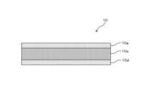
- FIG. 2 is a schematic cross-sectional view showing one configuration of a protective sheet.
- FIG. 1 is a schematic cross-sectional view showing an example of a semiconductor wafer.
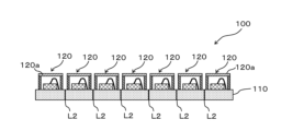
- FIG. 1 is a schematic cross-sectional view showing a configuration of a wafer level package.
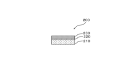
- FIG. 2 is a schematic cross-sectional view showing a configuration of an image sensor package.
- FIG. 2 is a schematic cross-sectional view showing a configuration of a laminate for an image sensor package.
- FIG. 4 is a schematic cross-sectional view showing another configuration of the protection sheet.
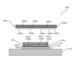
- FIG. 2 is a schematic cross-sectional view showing a state in which a semiconductor wafer is back-grinded.
- FIG. 1 is a schematic cross-sectional view showing an example of a semiconductor wafer.
- FIG. 1 is a schematic cross-sectional view showing a configuration of a wafer level package.
- FIG. 2 is a schematic cross-sectional view showing a configuration of an image sensor package.
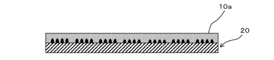
- FIG. 1 is a schematic cross-sectional view showing a configuration of a semiconductor wafer with a protective layer.
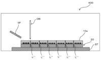
- 1 is a schematic cross-sectional view showing a first state when a semiconductor wafer with a protective layer is diced.
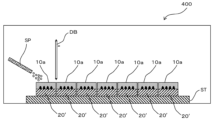
- FIG. 4 is a schematic cross-sectional view showing a second state when the semiconductor wafer with the protective layer is diced.
- the protective sheet according to one embodiment of the present invention may be simply referred to as the protective sheet according to this embodiment.
- the protective sheet according to the present embodiment includes a protective layer that is attached to a surface to be protected of an electronic component or a surface to be protected of an electronic component assembly in which a plurality of electronic components are connected together.
- a protective layer contains a water-soluble polymer compound.
- the protective layer has a viscosity ⁇ at 60° C. of 500,000 Pa ⁇ s or less.
- the protective sheet according to this embodiment includes a protective layer that is applied to the surface of an electronic component to be protected, or the surface of an electronic component assembly in which multiple electronic components are connected to be protected, and the protective layer contains at least one selected from the group consisting of polyvinyl alcohol, polyvinylpyrrolidone, and water-soluble polyester, and a polymer having a structural unit derived from ethylene oxide, as water-soluble polymer compounds.
- the protective layer of the protective sheet according to this embodiment can suppress the occurrence of thickness variations in the semiconductor wafer body of the semiconductor wafer when the semiconductor wafer is back-grinded.
- the protective sheet 10 according to the present embodiment includes a protective layer 10a.
- the protective sheet 10 according to the present embodiment further includes a base layer 10b disposed so as to face one surface of the protective layer 10a, and a pressure-sensitive adhesive layer 10c disposed between the protective layer 10a and the base layer 10b.
- one surface of the pressure-sensitive adhesive layer 10c facing the protective layer 10a and the other surface facing the base material layer 10b are releasably adhered to the protective layer 10a and the base material layer 10b, respectively.
- the electronic components include, for example, semiconductor chips and circuit boards. These electronic components are to be adherends of the protective layer 10a.
- the electronic component assembly may be, for example, a semiconductor wafer for obtaining a semiconductor chip, or a connected circuit board formed by connecting a plurality of circuit boards.
- An example of an electronic component device including the electronic component is a semiconductor device including a semiconductor chip.
- the semiconductor chip may be a TSV type semiconductor chip described later, or a sensor chip such as a CMOS chip.
- the semiconductor device including the CMOS chip may be configured to include a system LSI.
- the electronic component device may be a device including mechanical elements, sensors, actuators, or devices in which electronic circuits are integrated by microfabrication technology (MEMS (Micro Electro Mechanical Systems)) on a single substrate (e.g., a silicon substrate, a glass substrate, an organic material substrate, etc.).
- MEMS Micro Electro Mechanical Systems
- the electronic component device may be a device including a wiring board.
- the semiconductor wafer 20 shown in Fig. 2 includes a semiconductor wafer body 20a and a plurality of electrode portions 20b arranged on one surface of the semiconductor wafer body 20a.
- the one surface of the semiconductor wafer body 20a on which the plurality of electrode portions 20b are arranged is a circuit formation surface.
- a plurality of bump electrodes 20b1 are arranged at close intervals in each electrode portion 20b of the semiconductor wafer 20. That is, each electrode portion 20b is configured by a plurality of bump electrodes 20b1 arranged at high density.
- the bump electrodes 20b1 are usually formed by plating one surface of the semiconductor wafer main body 20a.
- the multiple electrode portions 20b are arranged so as to protrude from one surface of the semiconductor wafer main body 20a, as shown in FIG.
- the semiconductor wafer 20 is then divided (cut) along the cutting line L1 shown in Fig. 2 by dicing or the like, and is divided (cut into small pieces) into semiconductor chips each having at least one electrode portion 20b.
- the cutting line L1 for dividing (cutting) the semiconductor wafer main body 20a in Fig. 2 into individual pieces (small pieces) each having one electrode portion 20b is shown.
- the electrode portion 20b is electrically connected to an electrode portion of another member, such as a circuit board or another semiconductor chip configured similarly to the semiconductor chip.
- the semiconductor chip is classified as an electronic component.
- one surface of the semiconductor wafer body 20a is the surface to be protected.
- the surface on which the plurality of electrode portions 20b are arranged and which constitutes the circuit formation surface is the surface to be protected.
- a semiconductor wafer 20 (see FIG. 2) having a plurality of electrode portions 20b in which a plurality of bump electrodes 20b1 are arranged at close intervals may be used after each electrode portion 20b is attached to each semiconductor chip, and then each semiconductor chip is sealed with resin. 2 may be used as a substrate for a wafer level package (WLP), which is also classified as an electronic component assembly.
- WLP wafer level package
- the semiconductor chip may be, for example, a through silicon via (TSV) type semiconductor chip.
- TSV type semiconductor chip includes electrode parts that are arranged on both sides of the semiconductor chip body, form a pair, and are electrically connected to other members, and a conductive part that penetrates the semiconductor chip body in the thickness direction so as to conduct both electrode parts.
- only one surface may be a circuit formation surface, or both surfaces may be circuit formation surfaces.
- electrode portions are formed on both surfaces of the semiconductor chip body, both surfaces of the semiconductor chip body are surfaces to be protected.
- the semiconductor chip may also be a sensor chip in which the circuit has a sensor element (e.g., a light receiving element or a vibration element) as an element.
- a sensor chip is a CMOS (Complementary Metal-Oxide Semiconductor) chip.
- the electronic component assembly may also be a pseudo-wafer including a support substrate and a package formed by collectively sealing a plurality of semiconductor chips with resin while the plurality of semiconductor chips are arranged on the support substrate.
- the pseudo-wafer may be a package removed from the support substrate.
- a rewiring layer may be formed on at least one surface of the pseudo-wafer.
- the protective layer 10a of the protective sheet 10 may be used to protect the rewiring layer. Note that a pseudo-wafer divided into constituent units each including at least one semiconductor chip is classified as an electronic component.
- the wafer level package 100 shown in Fig. 3 includes a circuit board 110 and a plurality of semiconductor packages 120 mounted on the circuit board 110. That is, in the wafer level package 100, a plurality of semiconductor chips are individually sealed with resin on the circuit board 110.
- the surfaces (the surfaces farthest from the circuit board 110) of the semiconductor packages 120 may each be formed of one surface of the glass piece 120a. That is, in the wafer-level package 100, each semiconductor package 120 may have the glass piece 120a at the portion farthest from the circuit board 110.
- the protective layer 10 a of the protective sheet 10 is used to protect one side of each of the glass pieces 120 a of the multiple semiconductor packages 120 .
- the wafer level package 100 is divided (cut) along a cutting line L2 as shown in Fig. 3 by a dicing process or the like, and is divided into individual semiconductor packages. Each semiconductor package cut from the wafer level package 100 is classified as an electronic component.
- the wafer-level package 100 shown in FIG. 3 is sometimes called a panel-level package (PLP).
- the electronic component may be an image sensor package 200 as shown in Fig. 4A.
- the image sensor package 200 includes a sensor chip body 210 having a circuit formed on one surface thereof, and a glass piece 230 (cover glass) laminated on one surface (the surface on which the circuit is formed) of the sensor chip body 210.
- the sensor chip body 210 and the glass piece 230 (cover glass) are laminated via an adhesive layer 220 made of an adhesive, glass frit, or the like.
- the image sensor package 200 is used, for example, as an image pickup element for a camera or the like.
- the protective layer 10a of the protective sheet 10 is used to protect the surface of the glass piece 230 (the surface opposite to the sensor chip body 210 side).
- the image sensor package 200 is usually obtained by dividing the image sensor package laminate 200' by dicing or the like to separate into individual image sensor packages 200 each including at least one circuit.
- the image sensor package laminate 200' before being divided includes a sensor wafer main body 210' having a plurality of circuits formed on one surface thereof, and a glass plate 230' having approximately the same dimensions as the sensor wafer main body 210' in a plan view and laminated on one surface (the surface on which the plurality of circuits are formed) of the sensor wafer main body 210' via an adhesive layer 220' made of adhesive, glass frit, or the like.
- the image sensor package 200 is divided along the breaking lines L3 as shown in FIG. 4B by a dicing process, and is separated into individual image sensor packages 200.
- the stack 200' for an image sensor package is configured by connecting a plurality of image sensor packages 200 together, and is therefore classified as an electronic component assembly.
- the viscosity ⁇ of the protective layer 10a at 60°C is preferably 450,000 Pa ⁇ s or less, more preferably 400,000 Pa ⁇ s or less, even more preferably 300,000 Pa ⁇ s or less, particularly preferably 200,000 Pa ⁇ s or less, and more particularly preferably 150,000 Pa ⁇ s or less. Since the viscosity ⁇ of the protective layer 10a at 60°C is 150,000 Pa ⁇ s or less, at least one of the bump electrodes and the pillar terminals can be particularly suitably embedded in the protective layer 10a even when at least one of the bump electrodes and the pillar terminals is arranged at high density on one side of the semiconductor wafer body. The viscosity ⁇ of the protective layer 10a at 60° C.
- the viscosity ⁇ of the protective layer 10a at 60° C. is 30,000 Pa ⁇ s or more, when the surface to be protected of an electronic component or the like has a periphery and the protective layer 10a is attached along the periphery, the protective layer 10a is prevented from protruding from the periphery.
- the device when a device including an electronic component or the like is manufactured, the device can be prevented from being contaminated by a part of the protective layer 10a.
- the viscosity ⁇ of the protective layer 10a at 60°C can be increased, for example, by increasing the molecular weight of the water-soluble polymer compound contained in the protective layer 10a.
- the viscosity ⁇ of the protective layer 10a at 60°C can be decreased by decreasing the molecular weight of the water-soluble polymer compound contained in the protective layer 10a.
- the viscosity ⁇ of the protective layer 10a can be measured using a measuring device, Thermo Scientific HAAKE MARS III Rheometer, manufactured by Thermo Fisher Scientific. The following measurement conditions can be adopted.
- the viscosity is measured using a measurement sample whose thickness is adjusted to 300 ⁇ m by laminating a protective layer.
- Measurement sample 300 ⁇ m thick protective layer
- Probe diameter 8 mm
- Plate gap 250 ⁇ m
- Frequency 1Hz
- Measurement temperature 60°C
- water-soluble polymer compound examples include polyvinyl alcohol (PVA), polyvinylpyrrolidone (PVP), water-soluble polyester (PES), and polymers having a structural unit derived from ethylene oxide.
- PVA polyvinyl alcohol
- PVP polyvinylpyrrolidone
- PES water-soluble polyester
- the water-soluble polymer compound preferably contains at least one selected from the group consisting of polyvinyl alcohol, polyvinylpyrrolidone, and water-soluble polyester, and a polymer having a structural unit derived from ethylene oxide. More preferably, the water-soluble polymer compound contains at least one of polyvinyl alcohol and a water-soluble polyester, and a polymer having a structural unit derived from ethylene oxide.
- the mass ratio W1 is preferably 50 mass% or more.
- the mass ratio W1 may be 60 mass% or more, 70 mass% or more, or 80 mass% or more.
- the mass ratio W1 may be 95 mass% or less, or 90 mass% or less.
- the mass ratio W2 may be 5% by mass or more, or 10% by mass or more.
- the mass ratio W2 may be 50% by mass or less, 40% by mass or less, 30% by mass or less, or 20% by mass or less.
- the degree of saponification [mol %] of the polyvinyl alcohol is preferably 50 or more and 98 or less, and more preferably 60 or more and 90 or less. When the degree of saponification is within the above range, the polyvinyl alcohol exhibits sufficient water solubility.
- the protective layer forming composition for forming the protective layer 10a contains polyvinyl alcohol, the protective layer forming composition can be applied onto the release liner with good workability.
- the degree of saponification of the polyvinyl alcohol can be measured by proton magnetic resonance spectroscopy ( 1 H-NMR measurement method).
- the measurement sample is subjected to a methanol extraction treatment or the like to remove the additive, and then the degree of saponification of the polyvinyl alcohol is measured.
- the degree of saponification of the polyvinyl alcohol can be measured under the following conditions.
- VH methylene groups of the vinyl alcohol unit
- [VOH(--CH 2 )--] means the peak intensity derived from -CH 2 - in a vinyl alcohol unit
- [VAc(CH 3 CO--)] means the peak intensity derived from CH 3 CO-- in a vinyl acetate unit.
- the mass average molecular weight Mw of the polyvinyl alcohol is preferably 1,000 or more, more preferably 2,000 or more, further preferably 3,000 or more, and particularly preferably 4,000 or more. Such mass average molecular weight Mw may be 15,000 or less, 10,000 or less, 8,000 or less, or 6,000 or less. When the mass average molecular weight Mw is within the above range, the protective layer 10a having good shape retention can be formed with a more uniform thickness.
- the average polymerization degree of the polyvinyl alcohol is preferably 50 or more, more preferably 70 or more, and further preferably 90 or more. The average polymerization degree may be 1,000 or less, 800 or less, 600 or less, 400 or less, 200 or less, or 150 or less.
- the polyvinyl alcohol exhibits sufficient water solubility.
- the protective layer forming composition for forming the protective layer 10a contains polyvinyl alcohol, the protective layer forming composition can be applied onto the release liner with good workability.
- the weight average molecular weight Mw and the average degree of polymerization of the polyvinyl alcohol can be measured by aqueous gel permeation chromatography (aqueous GPC) under the following conditions. ⁇ Measurement conditions> ⁇ Analyzer Agilent, 1260Infinity Columns: TSKgel G6000PWXL (Tosoh Corporation) and TSKgel G3000PWXL (Tosoh Corporation) The two columns are connected in series.
- ⁇ Column temperature 40°C Eluent: 0.2M sodium nitrate solution
- Injection volume 100 ⁇ L
- ⁇ Standard samples PEG standard sample and PVA standard sample Specifically, the measurement is carried out as follows. (1) The weight average molecular weight Mw of the sample (PVA) and the PVA standard sample are calculated by GPC measurement using a PEG standard sample. The average degree of polymerization of the PVA standard sample is known. (2) A calibration curve is prepared using the average degree of polymerization of the PVA standard samples and the calculated mass average molecular weight Mw of the PVA standard samples. (3) Using the created calibration curve, the average degree of polymerization of the sample (PVA) is calculated from the mass average molecular weight Mw of the sample (PVA).
- polyvinyl alcohol When polyvinyl alcohol is used as the water-soluble polymer, multiple polyvinyl alcohols having different degrees of saponification may be used in combination, or multiple polyvinyl alcohols having different average degrees of polymerization may be used in combination.
- the water-soluble polyester has residues of a polycarboxylic acid and residues of a polyol.
- the water-soluble polyester is, for example, a polymerization product of a monomer mixture containing a polycarboxylic acid and a polyol.
- the water-soluble polyester can be determined to be water-soluble based on common technical knowledge.
- the water-soluble polyester preferably satisfies at least one of the following (1) to (4).
- (1) When room temperature (23 ⁇ 2° C.) water is sprayed onto the entire surface of a 20 ⁇ m-thick thin film formed from the water-soluble polyester at a spray pressure of 0.005 MPa for 20 minutes, the thin film dissolves entirely in water.
- (2) When water at 50° C. is sprayed onto the entire surface of a 20 ⁇ m-thick thin film formed from the water-soluble polyester for 10 minutes at a spray pressure of 0.005 MPa, the thin film dissolves entirely in water.
- the water-soluble polyester preferably has a mass average molecular weight Mw of 40,000 (forty thousand) or less.
- the protective layer-forming composition contains a water-soluble polyester having a mass average molecular weight Mw within the above numerical range, so that the protective layer 10a can be easily formed in a film-like form.
- the film-like protective layer 10a formed on the surface to be protected of the electronic component or the electronic component assembly can sufficiently suppress the adhesion of fine foreign matter to the surface to be protected.
- the water solubility of the protective layer 10a becomes better.
- the mass average molecular weight Mw of the water-soluble polyester is more preferably 30,000 (30,000) or less, more preferably 20,000 (20,000) or less, and even more preferably 15,000 or less.
- the water-soluble polyester may have a mass average molecular weight Mw of 5,000 or more, 7,000 or more, or 10,000 or more.
- the mass average molecular weight of the water-soluble polyester is measured by the same method (GPC measurement method) as the method for measuring the mass average molecular weight of polyvinyl alcohol described above.
- the polymer having a structural unit derived from ethylene oxide may be a homopolymer of ethylene oxide (EO), or a copolymer of ethylene oxide and an alkylene oxide other than ethylene oxide.
- the copolymer may be a random copolymer or a block copolymer.
- Examples of the alkylene oxide other than ethylene oxide include propylene oxide (PO) and butylene oxide (BO).
- the homopolymer of ethylene oxide (EO) may be polyethylene glycol (PEG) having a mass average molecular weight of less than 20,000, or polyethylene oxide (PEO) having a mass average molecular weight of 20,000 or more.
- PEG polyethylene glycol
- PEO polyethylene oxide
- Polyethylene oxide (PEO) is preferred in terms of suppressing the protrusion of the protective layer 10a described above.
- the mass average molecular weight of the polymer having structural units derived from ethylene oxide is measured by a method (GPC measurement method) similar to the method for measuring the mass average molecular weight of polyvinyl alcohol described above.
- GPC measurement method a method for measuring the mass average molecular weight of polyvinyl alcohol described above.
- PEG standard sample is used as the standard substance.
- the polymer having a structural unit derived from ethylene oxide is preferably a copolymer, and among the copolymers, a binary copolymer of ethylene oxide (EO) and propylene oxide (PO) is more preferable.
- a binary copolymer of ethylene oxide (EO) and propylene oxide (PO) is more preferable.
- the protective layer 10a contains a binary copolymer of ethylene oxide (EO) and propylene oxide (PO) as a polymer having a structural unit derived from ethylene oxide, it becomes even easier to adjust the viscosity ⁇ of the protective layer 10a to 500,000 Pa ⁇ s or less.
- the polymer having a structural unit derived from ethylene oxide is a binary copolymer of ethylene oxide (EO) and propylene oxide (PO)
- the molar ratio MR EO of the structural units derived from ethylene oxide (EO) is higher than the molar ratio MR PO of the structural units derived from propylene oxide (PO).
- the molar ratio MR EO of the structural units derived from ethylene oxide (EO) is preferably 55 mol % or more, more preferably 60 mol % or more, even more preferably 70 mol % or more, and particularly preferably 80 mol % or more.
- the upper limit of the molar ratio MR EO of the constituent units derived from ethylene oxide (EO) in the binary copolymer is, for example, 90 mol %.
- the molar ratio MR PO of the structural units derived from propylene oxide (PO) is preferably 45 mol % or less, more preferably 40 mol % or less, even more preferably 30 mol % or less, and particularly preferably 20 mol % or less.
- the lower limit of the molar ratio MR PO of the structural units derived from propylene oxide (PO) in the binary copolymer is, for example, 10 mol %.
- the mass average molecular weight Mw of the polymer having a structural unit derived from ethylene oxide may be 100,000 or more, 200,000 or more, 300,000 or more, or 400,000 or more.
- the mass average molecular weight Mw of the polymer having a structural unit derived from ethylene oxide may be 1,000,000 or less, 900,000 or less, 800,000 or less, 700,000 or less, or 600,000 or less.
- the mass average molecular weight of the polymer having a structural unit derived from ethylene oxide can be measured in the same manner as the mass average molecular weight Mw of polyvinyl alcohol described above.
- the viscosity of the aqueous solution containing the polymer having a structural unit derived from ethylene oxide is preferably 20 mPa ⁇ s or more, more preferably 30 mPa ⁇ s or more, and even more preferably 40 mPa ⁇ s or more, at a concentration of 2% by mass at 25° C. Furthermore, the viscosity of the aqueous solution at a concentration of 2% by mass at 25° C. may be 500 mPa ⁇ s or less, 400 mPa ⁇ s or less, or 300 mPa ⁇ s or less.
- the above viscosity can be measured using a digital viscometer (product name "DV-1 Prime”) manufactured by Eiko Seiki Co., Ltd. as a measuring device, using an LV-3 spindle at a rotation speed of 50 rpm.
- the protective layer 10a may contain, as water-soluble polymer compounds, a first water-soluble polymer compound and a second water-soluble polymer compound having a mass average molecular weight Mw greater than that of the first water-soluble polymer compound.
- the first water-soluble polymer compound preferably has a peak top P1 of the mass average molecular weight Mw in the range of 1,000 or more and 20,000 or less in peak analysis of the mass average molecular weight Mw based on gel permeation chromatography measurement (the above-mentioned GPC measurement).
- the second water-soluble polymer compound preferably has a peak top P2 of the mass average molecular weight Mw in the range of 100,000 or more and 1,000,000 or less.
- the peak top P1 is more preferably in the range of 2,000 to 15,000, even more preferably in the range of 3,000 to 8,000, and particularly preferably in the range of 4,000 to 6,000.
- the protective layer 10a can be adhered particularly well to the surface of the semiconductor wafer to be protected.
- the first water-soluble polymer compound can be dissolved particularly well in the composition for forming the protective layer for forming the protective layer 10a.
- the first water-soluble polymer compound having a peak top P1 within the above numerical range include polyvinyl alcohol, polyvinylpyrrolidone, and water-soluble polyester.
- the peak top P2 is more preferably in the range of 200,000 to 800,000, more preferably in the range of 300,000 to 700,000, and even more preferably in the range of 400,000 to 600,000.
- the protective layer 10a can have a good balance between both physical properties of mechanical strength and ductility, i.e., the protective layer 10a can have sufficient toughness.
- the second water-soluble polymer compound having a peak top P2 within the above numerical range may, for example, be a polymer having a structural unit derived from ethylene oxide.
- the proportion of the first water-soluble polymer compound in the total amount of the first water-soluble polymer compound and the second water-soluble polymer compound is preferably less than 90% by mass, more preferably 80% by mass or less, and is preferably 5% by mass or more, more preferably 10% by mass or more, and even more preferably 30% by mass or more.
- the base layer 10b supports the adhesive layer 10c.
- the base layer 10b is made using a metal foil, a fiber sheet, a rubber sheet, a resin film, or the like.
- the fiber sheet is made of, for example, paper, woven fabric, or nonwoven fabric.
- materials for the resin film include polyolefins such as polyethylene, polypropylene, and ethylene-propylene copolymers; ethylene copolymers such as ethylene-vinyl acetate copolymers, ionomer resins, ethylene-(meth)acrylic acid copolymers, ethylene-(meth)acrylic acid ester random copolymers, and ethylene-(meth)acrylic acid ester alternating copolymers; polyesters such as polyethylene terephthalate, polyethylene naphthalate, and polybutylene terephthalate; polyacrylates; polyvinyl chloride (PVC); polyurethanes; polycarbonates; polyphenylene sulfide; polyamides such as aliphatic polyamides and wholly aromatic polyamides (aramids); polyether ether ketones; polyimides; polyetherimides; polyvinylidene chloride; ABS (acrylonitrile-butadiene-styrene copolymers);
- the base layer 10b When the base layer 10b is made of a resin film, the base layer 10b may be obtained by non-stretch molding or by stretch molding, but is preferably obtained by stretch molding.
- the surface of the base layer 10b on which the pressure-sensitive adhesive layer 10c is laminated may be subjected to a surface treatment from the viewpoint of enhancing adhesion with the pressure-sensitive adhesive layer 10c.
- the surface treatment may employ a chemical method such as chromate treatment, ozone exposure, flame exposure, high-voltage shock exposure, or ionizing radiation treatment, or a physical method.
- a coating treatment using a coating agent such as an anchor coating agent, a primer, or an adhesive may be adopted.
- the surface of the base layer 10b on which the adhesive layer 10c is not laminated (hereinafter also referred to simply as the back surface) may be coated with a release agent (peeling agent) such as silicone resin or fluororesin to improve peelability.
- a release agent such as silicone resin or fluororesin to improve peelability.
- the thickness of the base material layer 10b is adjusted as appropriate depending on the manner in which the protective sheet 10 is used.
- the thickness of the base layer 10b may be 55 ⁇ m or more, or 60 ⁇ m or more.
- the thickness of the base layer 10b may be 195 ⁇ m or less, 190 ⁇ m or less, 170 ⁇ m or less, or 160 ⁇ m or less.
- the thickness of the base layer 10b can be determined, for example, by measuring the thickness at five randomly selected locations using a dial gauge (Model R-205, manufactured by PEACOCK) and calculating the arithmetic average of these measured values.
- the adhesive layer 10c has adhesiveness (pressure-sensitive adhesiveness) and can hold the protective layer 10a and the base layer 10b together by their adhesive strength.
- the adhesive layer 10c contains an adhesive to exert the adhesiveness described above.
- the adhesive may be, for example, one whose adhesive strength is reduced by external action during use of the protective sheet 10 (hereinafter also referred to as an adhesive-reducing type adhesive).
- the adhesive layer 10c can be in both a state exhibiting a relatively high adhesive strength (hereinafter referred to as a high-adhesion state) and a state exhibiting a relatively low adhesive strength (hereinafter referred to as a low-adhesion state) during the use of the protective sheet 10.
- a high-adhesion state a state exhibiting a relatively high adhesive strength
- a low-adhesion state a state exhibiting a relatively low adhesive strength
- the tack-reducing adhesive is, for example, an adhesive that can be cured by irradiation with active energy rays during use of the protective sheet 10 (hereinafter also referred to as an active energy ray curing adhesive).
- the tack-reducing adhesive contains a curing component that is cured by irradiation with active energy rays.
- the active energy ray curable adhesive may be, for example, an adhesive that is cured by irradiation with an electron beam, ultraviolet light, alpha rays, beta rays, gamma rays, or X-rays.
- an adhesive that is cured by ultraviolet light irradiation is preferred.
- the active energy ray-curable adhesive contains, for example, a base polymer as a main component, and an active energy ray-polymerizable monomer component or an active energy ray-polymerizable oligomer component having a functional group such as an active energy ray-polymerizable carbon-carbon double bond.
- the base polymer is preferably an acrylic polymer.
- the base polymer may be one that undergoes a polymerization reaction when irradiated with active energy rays to harden the pressure-sensitive adhesive layer 10c, thereby reducing the adhesive strength of the pressure-sensitive adhesive layer 10c.
- the acrylic polymer may include a monomer unit derived from a (meth)acrylic acid ester, such as a linear (meth)acrylic acid alkyl ester, a branched (meth)acrylic acid alkyl ester, a cyclic (meth)acrylic acid alkyl ester, or an aryl (meth)acrylic acid ester.
- a (meth)acrylic acid ester such as a linear (meth)acrylic acid alkyl ester, a branched (meth)acrylic acid alkyl ester, a cyclic (meth)acrylic acid alkyl ester, or an aryl (meth)acrylic acid ester.
- the monomer unit derived from the (meth)acrylic acid ester for example, 2-hydroxyethyl acrylate (HEA), ethyl acrylate (EA), butyl acrylate (BA), 2-ethylhexyl acrylate (2EHA), isononyl acrylate (iNA), lauryl acrylate (LA), 4-acryloylmorpholine (AMCO), 2-isocyanatoethyl methacrylate (MOI), etc. are preferably used.
- the monomer units derived from the (meth)acrylic acid ester may be of a single type or of a combination of two or more types.
- the acrylic polymer preferably contains, as monomer units derived from the (meth)acrylic acid ester, 2-ethylhexyl acrylate (2EHA), 2-hydroxyethyl acrylate (HEA), and 2-isocyanatoethyl methacrylate (MOI).
- 2-ethylhexyl acrylate (2EHA) 2-ethylhexyl acrylate
- HOA 2-hydroxyethyl acrylate
- MOI 2-isocyanatoethyl methacrylate
- the acrylic polymer may contain, as monomer units derived from a (meth)acrylic acid ester, lauryl acrylate (LA) and isononyl acrylate (iNA), in addition to 2EHA, HEA, and MOI.
- the pressure-sensitive adhesive layer 10c may contain an external crosslinking agent.
- the external crosslinking agent is not particularly limited as long as it can react with a base polymer (e.g., an acrylic polymer) to form a crosslinked structure.
- a base polymer e.g., an acrylic polymer
- Examples of such external crosslinking agents include polyisocyanate compounds, epoxy compounds, polyol compounds, aziridine compounds, and melamine-based crosslinking agents.
- Examples of the active energy ray-polymerizable monomer component include urethane (meth)acrylate, trimethylolpropane tri(meth)acrylate, pentaerythritol tri(meth)acrylate, pentaerythritol tetra(meth)acrylate, dipentaerythritol monohydroxypenta(meth)acrylate, dipentaerythritol hexa(meth)acrylate, and 1,4-butanediol di(meth)acrylate.
- Examples of the active energy ray-polymerizable oligomer component include various oligomers such as urethane-based oligomers, polyether-based oligomers, polyester-based oligomers, polycarbonate-based oligomers, polybutadiene-based oligomers, etc.
- the content of the active energy ray-polymerizable monomer component or the active energy ray-polymerizable oligomer component in the active energy ray-curable adhesive is selected within a range that appropriately reduces the adhesiveness of the adhesive layer 10c.
- the active energy ray-curable adhesive preferably contains a photopolymerization initiator, such as an azo compound, an ⁇ -ketol compound, an acetophenone compound, a benzoin ether compound, a ketal compound, an aromatic sulfonyl chloride compound, a photoactive oxime compound, a benzophenone compound, a thioxanthone compound, camphorquinone, a halogenated ketone, an acylphosphinoxide, or an acylphosphonate.
- a photopolymerization initiator such as an azo compound, an ⁇ -ketol compound, an acetophenone compound, a benzoin ether compound, a ketal compound, an aromatic sulfonyl chloride compound, a photoactive oxime compound, a benzophenone compound, a thioxanthone compound, camphorquinone, a halogenated ketone, an acylphosphinoxid
- the pressure-sensitive adhesive layer 10c when the pressure-sensitive adhesive layer 10c contains an external crosslinking agent, the pressure-sensitive adhesive layer 10c preferably contains the external crosslinking agent in an amount of 0.1% by mass or more and 3.0% by mass or less.
- the pressure-sensitive adhesive layer 10c when the pressure-sensitive adhesive layer 10c contains a photopolymerization initiator, the pressure-sensitive adhesive layer 10c preferably contains 0.1% by mass or more and 10.0% by mass or less of the photopolymerization initiator.
- the adhesive layer 10c may contain a crosslinking promoter, a tackifier, an anti-aging agent, a pigment, a colorant such as a dye, etc.
- the thickness of the pressure-sensitive adhesive layer 10c is preferably 1 ⁇ m or more and 50 ⁇ m or less, more preferably 2 ⁇ m or more and 30 ⁇ m or less, and even more preferably 5 ⁇ m or more and 25 ⁇ m or less.
- the thickness of the adhesive layer 10c can be determined, for example, by measuring the thickness at five randomly selected locations using a dial gauge (Model R-205, manufactured by PEACOCK) and calculating the arithmetic average of these measured values.
- an adhesive whose adhesive strength can be reduced by external action during use of the protective sheet 10 has been described.
- An example of such an adhesive is an adhesive that can be cured by irradiation with active energy rays, but the adhesive is not limited to this.
- the adhesive may be a pressure-sensitive adhesive that does not cure by irradiation with active energy rays.
- the protective sheet 10 can be produced, for example, by bonding the protective layer 10a to a laminated sheet body in which the base layer 10b and the adhesive layer 10c are laminated.
- the protective sheet 10 can be produced by bonding the protective layer 10a to the adhesive layer 10c of the laminated sheet body.
- the laminated sheet can be prepared, for example, by applying an adhesive composition, in which the above-mentioned components for forming the adhesive layer 10c are dissolved or suspended in an organic solvent (e.g., toluene, etc.), to the base layer 10b.
- an adhesive composition in which the above-mentioned components for forming the adhesive layer 10c are dissolved or suspended in an organic solvent (e.g., toluene, etc.
- the adhesive composition is applied to one side of the base layer 10b in a predetermined thickness (e.g., 10 ⁇ m) using an applicator or the like.
- the laminated sheet can be prepared by drying at a predetermined temperature for a predetermined time (e.g., 120° C. for 2 minutes).
- the protective layer 10a can be formed on one side of a release liner.
- a composition for forming a protective layer is prepared by dissolving or suspending the components for forming the protective layer 10a in water.
- the composition for forming a protective layer is applied to the release-treated surface of the release liner in a predetermined thickness (e.g., 40 ⁇ m) using an applicator or the like.
- the protective layer 10a can then be formed by drying at a predetermined temperature for a predetermined time (e.g., at 115° C. for 90 seconds).
- the protective layer 10a formed on the release-treated surface of the release liner is attached to the pressure-sensitive adhesive layer 10c of the laminated sheet body.
- the release liner is then peeled off from the protective layer 10a to obtain the protective sheet 10 in which the base layer 10b, the pressure-sensitive adhesive layer 10c, and the protective layer 10a are laminated in this order.
- the protective sheet 10 is formed by laminating the base layer 10b, the adhesive layer 10c, and the protective layer 10a in this order (see FIG. 1 ), but the protective sheet 10 is not limited to this example.
- protective sheet 10 may include protective layer 10a, a first release liner 10d overlying one side of protective layer 10a, and a second release liner 10e overlying the other side of protective layer 10a. That is, protective sheet 10 may be configured such that protective layer 10a is sandwiched from both sides by a pair of release liners (first release liner 10d and second release liner 10e).
- protective sheet 10 may include only protective layer 10a without including substrate layer 10b, pressure-sensitive adhesive layer 10c, first release liner 10d, second release liner 10e, etc.
- protective sheet 10 includes at least protective layer 10a.
- the first release liner 10d may be, for example, a base sheet made of a resin such as polyethylene terephthalate (PET) and the like, which has been subjected to a release treatment.
- PET polyethylene terephthalate
- the second release liner 10e may be the same as the first release liner 10d.
- An example of the release liner is "MRA50" manufactured by Mitsubishi Chemical Corporation.
- each of the first release liner 10d and the second release liner 10e is preferably 15 ⁇ m or more and 75 ⁇ m or less, and more preferably 20 ⁇ m or more and 60 ⁇ m or less.
- the thickness of the first release liner 10d and the thickness of the second release liner 10e may be the same as or different from each other.
- the thicknesses of the first release liner 10d and the second release liner 10e can be determined in the same manner as the thickness of the protective layer 10a described above.
- the protective sheet 10 according to the present embodiment is used, for example, when the electronic component assembly is subjected to back-grinding in order to reduce the thickness of the electronic component assembly by grinding. Moreover, the protective sheet 10 according to the present embodiment is also used when the electronic component assembly is subjected to a dicing process in order to cut the electronic component assembly and separate it into a plurality of electronic components (small pieces).
- a dicing process in order to cut the electronic component assembly and separate it into a plurality of electronic components (small pieces).
- each of the plurality of electrode portions 20b is configured by a plurality of bump electrodes 20b1 arranged at close intervals. That is, each of the plurality of electrode portions 20b is configured by a plurality of bump electrodes 20b1 arranged at high density.
- the back-grinding process for the semiconductor wafer 20 is performed using a back-grinding device 300 as shown in Fig. 6.
- the back-grinding device 300 includes a suction plate 310 and a polishing head 320 disposed to face the suction plate 310.
- the suction plate 310 is, for example, a vacuum chuck that suctions and holds an object by reducing pressure.
- the semiconductor wafer 20, one surface of which of the semiconductor wafer body 20a is protected by the protective layer 10a of the protective sheet 10, is suction-held on the suction plate 310.
- the other surface of the semiconductor wafer body 20a (the surface opposite to the surface on which the electrode portion 20b is arranged) becomes the grinding surface.
- one surface of the semiconductor wafer body 20a is protected by the protective layer 10a in a temperature environment of 60° C. so that the electrode portions 20b protruding from one surface of the semiconductor wafer body 20a are embedded therein.
- the viscosity ⁇ of the protective layer 10a is a relatively low value of 500,000 Pa ⁇ s or less at 60° C. Therefore, even if the multiple bump electrodes 20b1 are densely arranged in each of the multiple electrode parts 20b arranged on one surface of the semiconductor wafer main body 20a, the multiple electrode parts 20b can be sufficiently embedded inside the protective layer 10a.
- the polishing head 320 includes a polishing head body 320a and a plurality of abrasive grains 320b protruding from one surface of the polishing head body 320a.
- the semiconductor wafer body 20a is ground by the abrasive grains 320b of the polishing head body 320a, while thinning the semiconductor wafer body 20a to a predetermined thickness.
- the semiconductor wafer 20 is removed from the suction plate 310 with the protective sheet 10 attached to one side of the semiconductor wafer main body 20a.
- the adhesive layer 10c is made of an adhesive that can be cured by irradiation with active energy rays, active energy rays are irradiated from the base layer 10b side of the protective sheet 10. Such irradiation makes the adhesive layer 10c in a low-adhesion state.
- the protective layer 10a is peeled off from the adhesive layer 10c to obtain the semiconductor wafer 20 with only the protective layer 10a attached, as shown in FIG. 7.
- the semiconductor wafer 20 shown in FIG. 7 will be referred to as a semiconductor wafer 20 with a protective layer 10a.
- the dicing process of the semiconductor wafer 20 is performed using a blade dicing device 400 as shown in Fig. 8A.
- the blade dicing device 400 includes a stage ST, a liquid spraying part SP, and a dicing blade DB.
- dicing is performed using a semiconductor wafer 20 with a protective layer 10a as shown in FIG.
- the semiconductor wafer 20 with the protective layer 10a is placed on the stage ST of the blade dicing device 400 so that the stage ST and the exposed surface of the semiconductor wafer 20 (the surface opposite to the surface coated with the protective layer 10a) are in contact with each other.
- cooling water is sprayed from the liquid spray unit SP to wash the semiconductor wafer with the protective layer 10a with water, while the semiconductor wafer with the protective layer 10a is divided by the dicing blade DB.
- the semiconductor wafer with the protective layer 10a is divided so that each individual piece after division has at least one electrode portion 20b.
- the semiconductor wafer 20 with the protective layer 10a is cut into individual pieces by a dicing blade DB along a cutting line L'' shown in FIG. 8A.
- the semiconductor wafer 20 is divided so that each individual piece after division has one electrode portion 20b.
- the protective layer 10a is also divided into chip-sized pieces together with the semiconductor wafer 20 by the dicing blade DB. As described above, by performing the blade dicing process while spraying cooling water, at least a portion of each divided piece of the protective layer 10a can be dissolved.
- the semiconductor wafer main body 20a the surface on which the electrode portion 20b is arranged
- the divided pieces of the protective layer 10a can be further washed with water (cold water or hot water), thereby removing the divided pieces of the protective layer 10a from the plurality of semiconductor chips 20'.
- a protective layer that is attached to a surface to be protected of an electronic component or to a surface to be protected of an electronic component assembly in which a plurality of the electronic components are connected together; the protective layer contains a water-soluble polymer compound,
- the viscosity ⁇ of the protective layer is 500,000 Pa ⁇ s or less at 60° C.
- Protective sheet
- the protective layer contains, as the water-soluble polymer compound, a first water-soluble polymer compound and a second water-soluble polymer compound having a mass average molecular weight larger than that of the first water-soluble polymer compound;
- the peak top of the mass average molecular weight of the first water-soluble polymer compound is in a range of 1,000 to 20,000
- the peak top of the mass average molecular weight of the second water-soluble polymer compound is in a range of 100,000 to 1,000,000.
- a protective layer that is attached to a surface to be protected of an electronic component or to a surface to be protected of an electronic component assembly in which a plurality of the electronic components are connected together;
- the protective layer contains, as a water-soluble polymer compound, at least one of polyvinyl alcohol and a water-soluble polyester, and a polymer having a structural unit derived from ethylene oxide;
- Protective sheet contains, as a water-soluble polymer compound, at least one of polyvinyl alcohol and a water-soluble polyester, and a polymer having a structural unit derived from ethylene oxide;
- a base layer disposed so as to face one surface of the protective layer;
- a pressure-sensitive adhesive layer is disposed between the protective layer and the base layer, Both sides of the pressure-sensitive adhesive layer are releasably adhered to the protective layer and the base layer, respectively.
- the protective sheet according to any one of (1) to (3) above.
- the protective sheet according to the present invention is not limited to the above-mentioned embodiment. Furthermore, the protective sheet according to the present invention is not limited by the above-mentioned effects. The protective sheet according to the present invention can be modified in various ways without departing from the gist of the present invention.
- protective sheet 10 has been described in which protective layer 10a is attached to semiconductor wafer 20, which is an electronic component assembly, but the attachment target is not limited to this.
- the attachment target may be, for example, a wafer level package 100 (see FIG. 3) serving as an electronic component assembly, or may be a laminate 200' for an image sensor package (see FIG. 4B). That is, the protective sheet 10 may be used when performing back-grinding on the circuit board 110 of the wafer level package 100, or when dividing the wafer level package 100 into a plurality of semiconductor packages 120.
- the protective sheet 10 may also be used when performing back-grinding on the sensor wafer main body 210' of the laminate 200' for an image sensor package, or when dividing the laminate 200' for an image sensor package into a plurality of image sensor packages 200.
- [EO/PO copolymer-1] A binary copolymer of ethylene oxide (EO) and propylene oxide (PO) (EO/PO binary copolymer) Product name "ALKOX (registered trademark) EP1550H” manufactured by Meisei Chemical Industry Co., Ltd. (EO molar ratio: 85%, PO molar ratio: 15%, mass average molecular weight Mw: 500,000)
- EO/PO copolymer-2 A binary copolymer of ethylene oxide (EO) and propylene oxide (PO) (EO/PO binary copolymer) Product name "ALKOX (registered trademark) EP1010N” manufactured by Meisei Chemical Industry Co., Ltd.
- Example 1 In a container, polyvinyl alcohol (PVA) and a binary copolymer of ethylene oxide (EO) and propylene oxide (PO) (EO/PO binary copolymer) were dispersed in water to prepare an aqueous dispersion solution.
- the aqueous dispersion solution was prepared so that the mass ratio of PVA:EO/PO binary copolymer was 90:10.
- the polyvinyl alcohol used was the above-mentioned "PVA-1.”
- the EO/PO binary copolymer used was the above-mentioned "EO/PO copolymer-1.”
- the container containing the above aqueous dispersion was placed in a water bath at 90° C., and the aqueous dispersion was stirred to dissolve the polyvinyl alcohol in water, thereby obtaining a composition for forming a protective layer.
- the composition for forming a protective layer was applied using an applicator to the release-treated surface of a PET release liner (manufactured by Mitsubishi Chemical Corporation, product name "MRA50", thickness 50 ⁇ m) having a silicone release-treated surface, so that the thickness after drying was 30 ⁇ m.
- the protective layer-forming composition on the PET release liner was dried at 115° C. for 90 seconds to form a protective layer having a thickness of 30 ⁇ m on the PET release liner.
- the release-treated surface of another PET release liner (the same product as above) was attached to the exposed surface of the protective layer.
- the protective sheet was made by laminating a PET release liner, a 30 ⁇ m-thick protective layer, and a PET release liner in this order.
- a protective layer having a thickness of 300 ⁇ m was prepared by laminating three protective layers each having a thickness of 100 ⁇ m.
- the above protective layer-forming composition was applied to the release-treated surface of a PET release liner (same as above) using an applicator in the same manner as above, so that the thickness after drying would be 100 ⁇ m.
- a protective layer having a thickness of 100 ⁇ m was formed on the PET release liner by drying at 130° C. for 300 seconds. This operation was repeated three times in total to obtain three PET release liners with protective layers.
- a second PET release liner with a protective layer was laminated on the exposed surface of the protective layer of the first PET release liner with a protective layer to obtain a laminate, i.e., a laminate having two protective layers laminated thereon was obtained. Furthermore, in this laminate, the PET release liner was peeled off from the second PET release liner with protective layer to expose the protective layer, and then the protective layer of the third PET release liner with protective layer was superposed on the exposed surface to obtain a further laminate, i.e., a laminate with three protective layers stacked was obtained. Then, the laminate was heat-treated at a temperature of 90° C. using a laminator. This produced a protective sheet having a protective layer with a thickness of 300 ⁇ m. That is, the protective sheet was composed of a PET release liner, a 300 ⁇ m thick protective layer, and another PET release liner laminated in this order.
- the mass average molecular weight Mw, the degree of saponification, and the average degree of polymerization of the PVA were each measured according to the methods described in the above embodiment section.
- the mass average molecular weight Mw of each of the EO/PO binary copolymers was measured according to the method described in the above embodiment section.
- the molar ratio of EO and the molar ratio of PO are the molar ratios at the start of polymerization.
- the viscosity ⁇ of the protective layer at 60° C. was measured using a protective layer having a thickness of 300 ⁇ m.
- the viscosity ⁇ was measured according to the method described in the embodiment section above. The results are shown in Table 1.
- a protective sheet having a PET release liner, a 30 ⁇ m thick protective layer, and a PET release liner laminated in that order and a protective sheet having a PET release liner, a 300 ⁇ m thick protective layer, and a PET release liner laminated in that order were respectively produced. Furthermore, the viscosity ⁇ of the protective layer at 60° C. was measured using a protective sheet having a thickness of 300 ⁇ m. The viscosity ⁇ was measured according to the method described in the embodiment section above. The results are shown in Table 1.
- Example 3 A protective layer-forming composition was obtained in the same manner as in Example 2, except that a water-soluble polyester (PES) was used instead of PVA. The above-mentioned product was used as the PES. Furthermore, using this protective layer-forming composition, a protective sheet having a protective layer with a thickness of 30 ⁇ m and a protective sheet having a protective layer with a thickness of 300 ⁇ m were obtained in the same manner as in Example 1. That is, a protective sheet having a PET release liner, a 30 ⁇ m thick protective layer, and a PET release liner laminated in that order, and a protective sheet having a PET release liner, a 300 ⁇ m thick protective layer, and a PET release liner laminated in that order were respectively produced. Furthermore, the viscosity ⁇ of the protective layer at 60° C. was measured using a protective layer with a thickness of 300 ⁇ m. The viscosity ⁇ was measured according to the method described in the embodiment section above. The results are shown in Table 1.
- Example 4 A protective layer-forming composition was obtained at the same mass ratio of PVA and EO/PO binary copolymer as in Example 2. Next, using this protective layer-forming composition, a protective layer was formed on a PET release liner so that the thickness after drying was 5 ⁇ m, in the same manner as in Example 1, to obtain a protective layer with a release liner. Separately, a protective layer was formed on a PET release liner so that the thickness after drying was 60 ⁇ m, to obtain another protective layer with a release liner. Next, a dicing tape was prepared. Specifically, a dicing tape manufactured by Nitto Denko Corporation with a product name of "UB-3200F" (substrate layer thickness 100 ⁇ m, adhesive layer thickness 100 ⁇ m) was prepared.
- the viscosity ⁇ of the protective layer at 60° C. was measured using a protective layer (thickness 60 ⁇ m) with a release liner.
- the viscosity ⁇ was measured according to the method described in the above embodiment section. The results are shown in Table 1.
- the exposed surface of the adhesive layer of the dicing tape was superposed on the exposed surface of the protective layer (thickness 5 ⁇ m) with a release liner to obtain a laminated sheet.
- the laminated sheet was processed using a laminating roll at a temperature of 25° C. and a speed of 10 mm/s to obtain a protective sheet with a protective layer of 5 ⁇ m in thickness. That is, the protective sheet was a laminate of the base layer, the adhesive layer, the protective layer of 5 ⁇ m in thickness, and the PET release liner in this order.
- the exposed surface of the adhesive layer of the dicing tape was superposed on the exposed surface of the protective layer (60 ⁇ m thick) with a release liner to obtain another laminated sheet.
- the laminated sheet was treated in the same manner as above using a laminating roll to obtain a protective sheet with a 60 ⁇ m thick protective layer. That is, the protective sheet was a laminate of the base layer, the adhesive layer, the 60 ⁇ m thick protective layer, and the PET release liner in this order.
- Example 1 A composition for forming a protective layer was obtained in the same manner as in Example 1, except that only PVA was dispersed in water.
- a protective sheet having a protective layer with a thickness of 30 ⁇ m was obtained using the composition for forming a protective layer in the same manner as in Example 1.
- a protective sheet having a protective layer with a thickness of 300 ⁇ m was obtained in the same manner. That is, a protective sheet having a PET release liner attached to one side of a protective layer with a thickness of 30 ⁇ m and a protective sheet having a PET release liner attached to one side of a protective layer with a thickness of 300 ⁇ m were each produced. Furthermore, the viscosity ⁇ of the protective layer at 60° C. was measured using a protective layer with a thickness of 300 ⁇ m. The viscosity ⁇ was measured according to the method described in the embodiment section above. The results are shown in Table 1.
- Example 5 A composition for forming a protective layer was obtained in the same manner as in Example 1, except that an aqueous dispersion was prepared by dispersing PVA and EO/PO binary copolymer in water so that the mass ratio of PVA:EO/PO binary copolymer was 75:25, that the above-mentioned "PVA-2” was used as the PVA, and that the above-mentioned "EO/PO copolymer-2” was used as the EO/PO binary copolymer. Furthermore, in the same manner as in Example 1, a protective sheet having a protective layer with a thickness of 30 ⁇ m and a protective sheet having a protective layer with a thickness of 300 ⁇ m were obtained.
- a protective sheet was produced in which a PET release liner, a 30 ⁇ m thick protective layer, and a PET release liner were laminated in that order, and a protective sheet was produced in which a PET release liner, a 300 ⁇ m thick protective layer, and a PET release liner were laminated in that order. Furthermore, the viscosity ⁇ of the protective layer at 60° C. was measured using a protective layer with a thickness of 300 ⁇ m. The viscosity ⁇ was measured according to the method described in the embodiment section above. The results are shown in Table 2.
- Example 6 A composition for forming a protective layer was obtained in the same manner as in Example 1, except that PES and EO/PO binary copolymer were dispersed in water to prepare an aqueous dispersion so that the mass ratio of PES:EO/PO binary copolymer was 75:25, and the above-mentioned "EO/PO copolymer-2" was used as the EO/PO binary copolymer. Furthermore, in the same manner as in Example 1, a protective sheet having a protective layer with a thickness of 30 ⁇ m and a protective sheet having a protective layer with a thickness of 300 ⁇ m were obtained.
- a protective sheet having a PET release liner, a 30 ⁇ m thick protective layer, and a PET release liner laminated in that order and a protective sheet having a PET release liner, a 300 ⁇ m thick protective layer, and a PET release liner laminated in that order were produced. Furthermore, the viscosity ⁇ of the protective layer at 60° C. was measured using a protective layer having a thickness of 300 ⁇ m. The viscosity ⁇ was measured according to the method described in the embodiment section above. The results are shown in Table 2.
- Example 7 A composition for forming a protective layer was obtained in the same manner as in Example 1, except that PES and polyethylene oxide were dispersed in water to prepare an aqueous dispersion so that the mass ratio of PES:polyethylene oxide was 75:25, and the above-mentioned "PEO" was used as the polyethylene oxide. Furthermore, in the same manner as in Example 1, a protective sheet having a protective layer with a thickness of 30 ⁇ m and a protective sheet having a protective layer with a thickness of 300 ⁇ m were obtained.
- a protective sheet having a PET release liner, a 30 ⁇ m thick protective layer, and a PET release liner laminated in that order and a protective sheet having a PET release liner, a 300 ⁇ m thick protective layer, and a PET release liner laminated in that order were produced. Furthermore, the viscosity ⁇ of the protective layer at 60° C. was measured using a protective layer having a thickness of 300 ⁇ m. The viscosity ⁇ was measured according to the method described in the embodiment section above. The results are shown in Table 2.
- Example 8 A composition for forming a protective layer was obtained in the same manner as in Example 1, except that an aqueous dispersion was prepared by dispersing PVA and polyethylene glycol in water so that the mass ratio of PVA:polyethylene glycol was 75:25, that the above-mentioned "PVA-2” was used as the PVA, and that the above-mentioned "PEG600” was used as the polyethylene glycol. Furthermore, in the same manner as in Example 1, a protective sheet having a protective layer with a thickness of 30 ⁇ m and a protective sheet having a protective layer with a thickness of 300 ⁇ m were obtained.
- a protective sheet having a PET release liner, a 30 ⁇ m thick protective layer, and a PET release liner laminated in that order and a protective sheet having a PET release liner, a 300 ⁇ m thick protective layer, and a PET release liner laminated in that order were produced. Furthermore, the viscosity ⁇ of the protective layer at 60° C. was measured using a protective layer having a thickness of 300 ⁇ m. The viscosity ⁇ was measured according to the method described in the embodiment section above. The results are shown in Table 2.
- Example 9 A composition for forming a protective layer was obtained in the same manner as in Example 1, except that PES and polyethylene glycol were dispersed in water to prepare an aqueous dispersion so that the mass ratio of PES:polyethylene glycol was 75:25, and that the above-mentioned "PEG2000" was used as the polyethylene glycol. Furthermore, in the same manner as in Example 1, a protective sheet having a protective layer with a thickness of 30 ⁇ m and a protective sheet having a protective layer with a thickness of 300 ⁇ m were obtained.
- a protective sheet having a PET release liner, a 30 ⁇ m thick protective layer, and a PET release liner laminated in that order and a protective sheet having a PET release liner, a 300 ⁇ m thick protective layer, and a PET release liner laminated in that order were produced. Furthermore, the viscosity ⁇ of the protective layer at 60° C. was measured using a protective layer having a thickness of 300 ⁇ m. The viscosity ⁇ was measured according to the method described in the embodiment section above. The results are shown in Table 2.
- Example 10 A composition for forming a protective layer was obtained in the same manner as in Example 1, except that an aqueous dispersion was prepared by dispersing PES and polyethylene glycol in water so that the mass ratio of PES:polyethylene glycol was 75:25, and that the above-mentioned "PEG 600" was used as the polyethylene glycol. Furthermore, in the same manner as in Example 1, a protective sheet having a protective layer with a thickness of 30 ⁇ m and a protective sheet having a protective layer with a thickness of 300 ⁇ m were obtained.
- a protective sheet having a PET release liner, a 30 ⁇ m thick protective layer, and a PET release liner laminated in that order and a protective sheet having a PET release liner, a 300 ⁇ m thick protective layer, and a PET release liner laminated in that order were produced. Furthermore, the viscosity ⁇ of the protective layer at 60° C. was measured using a protective layer having a thickness of 300 ⁇ m. The viscosity ⁇ was measured according to the method described in the embodiment section above. The results are shown in Table 2.
- Each of the above protective sheets was evaluated for embeddability in a semiconductor chip having a plurality of bump electrodes on one surface (hereinafter referred to as a semiconductor chip with bump electrodes) (Evaluation 1 of embeddability).
- a semiconductor wafer (hereinafter also referred to as a semiconductor wafer with bump electrodes) was divided to obtain a plurality of semiconductor chips with bump electrodes as follows.
- the semiconductor wafer with bump electrodes before division had a plurality of regions (3 mm x 3 mm regions) on one side in which a plurality of bump electrodes each having a diameter (bump diameter) of 45 ⁇ m in top view were arranged with a spacing (bump pitch) between adjacent bump electrodes of 150 ⁇ m.
- Each semiconductor chip with bump electrodes was cut out from this semiconductor wafer with bump electrodes so as to include one of the plurality of regions and have a planar dimension of 5 mm x 5 mm.
- the protective layer after the PET release liner was peeled off was used in evaluation 1 of embeddability.
- each bump electrode was provided so that the height from one surface of the semiconductor wafer body provided on the semiconductor wafer to the tip was 40 ⁇ m.
- Evaluation 1 of embeddability the protective layer of each of the above protective sheets was attached to one surface of the semiconductor wafer body under conditions of a pressure (lamination pressure) of 0.4 MPa and a roller temperature of 60°C. Evaluation 1 of embeddability was performed by observation with a digital microscope according to the following criteria. The evaluation results of Evaluation 1 of Embeddability are shown in Table 1. Excellent: No optical interference was observed. In other words, each bump electrode was completely and sufficiently embedded inside the protective layer. Good: Some optical interference is observed in the outer periphery of each bump electrode. In other words, the vicinity of the top of each bump electrode is sufficiently embedded in the protective layer, but the outer periphery of each bump electrode is not sufficiently embedded. Poor: Clear voids are observed around the periphery of each bump electrode. In other words, even the top portions of each bump electrode are not fully embedded in the protective layer.
- test specimen having a step was prepared by stacking two bare wafers having different planar dimensions and thicknesses in the thickness direction. Then, the embeddability of each of the protective sheets in the test specimen having the step was evaluated (Evaluation of Embeddability 2).
- the test specimen having the step was prepared by laminating a first bare wafer having an outer diameter of 10 mm and a thickness of 700 ⁇ m and a second bare wafer having an outer diameter of 5 mm and a thickness of 300 ⁇ m with a die bond film having a thickness of 10 ⁇ m interposed therebetween. That is, the test specimen having the step had a step of 310 ⁇ m in height.
- the protective layer after peeling off the PET release liner was also used.
- the protective layer of each of the above protective sheets was adhered to one surface (the surface having the step) of a test specimen having a step under conditions of a pressure (lamination pressure) of 0.4 MPa and a roller temperature of 60°C.
- the horizontal distance HD between the corner where the periphery of the second bare wafer contacts one side of the first bare wafer and the protective layer facing the corner was measured using a digital microscope.
- the evaluation was performed according to the following evaluation criteria.
- the evaluation results of the evaluation 2 of the embeddability are shown in Table 1. Excellent: The horizontal distance HD is 1.0 mm or less. Good: The horizontal distance HD is more than 1.0 mm and is 2.0 mm or less. Unacceptable: The horizontal distance HD exceeds 2.0 mm or the protective layer is damaged.
- aqueous dispersion was prepared by dispersing PVA and EO/PO binary copolymer in water so that the mass ratio of PVA:EO/PO binary copolymer was 5:95.
- the above-mentioned "PVA-1” was used as the PVA, and the above-mentioned "EO/PO copolymer-1” was used as the EO/PO binary copolymer.
- a composition for forming a protective layer was obtained in the same manner as in Example 1.
- a protective layer having a thickness of 30 ⁇ m was formed on the PET release liner in the same manner as in Example 1.
- a protective sheet was obtained in which the PET release liner, the protective layer having a thickness of 30 ⁇ m, and the PET release liner were laminated in this order.
- a protective layer having a thickness of 300 ⁇ m was formed on a PET release liner in the same manner as in Example 1. That is, a protective sheet in which a PET release liner, a protective layer having a thickness of 300 ⁇ m, and a PET release liner were laminated in this order was further obtained.
- the protective sheet according to the reference example received an "excellent" result in both embeddability evaluation 1 and embeddability evaluation 2.
- the protective sheet of the present invention is preferably used, for example, as an auxiliary tool when manufacturing electronic component devices such as semiconductor devices.
- the method of manufacturing electronic component devices of the present invention is preferably used, for example, when manufacturing electronic component devices such as semiconductor devices.
- 10 protective sheet, 10a: protective layer, 10b: base layer, 10c: adhesive layer, 10d: first release liner, 10e: second release liner, 20: semiconductor wafer, 20a: semiconductor wafer body, 20b: electrode portion, 20b1: bump electrode, 20': semiconductor chip, 100: wafer level package, 110: circuit board, 120: semiconductor package, 120a: glass piece, 200: Image sensor package; 210: Sensor chip body; 220: Adhesive layer; 230: Glass piece; 200': laminate for image sensor package; 210': sensor wafer body; 220': adhesive layer; 230': glass plate; 300: back grinding device, 310: suction plate, 320: polishing head, 320a: polishing head body; 320b: abrasive grains; 400: Blade dicing device, DB: dicing blade, SP: liquid spray part, ST: stage.
Landscapes
- Chemical & Material Sciences (AREA)
- Organic Chemistry (AREA)
- Adhesive Tapes (AREA)
- Laminated Bodies (AREA)
Abstract
Description
電子部品装置が半導体装置である場合、保護対象物は、例えば半導体ウエハである。保護シートは、半導体装置の製造工程中に、保護対象物である半導体ウエハの表面の少なくとも一部に被着されて使用される。
なお、半導体ウエハにおいて、高集積の電子回路が形成された面(一方の面)は、回路面又は回路形成面とも称される。
詳しくは、前記半導体ウエハ本体の他方の面(回路形成面の反対面)側から半導体ウエハ本体を研削するバックグラインド加工によって、半導体ウエハ本体を所定の厚さまで薄くする場合がある。
このような半導体ウエハの研削においては、研磨ヘッドからの押圧力によって、複数の電極部が吸着プレートの表面に押し付けられる。斯かる力によって複数の電極が破損することを抑制すべく、半導体ウエハ本体の一方の面は、例えば、水溶性高分子化合物を含む保護層を介在させた状態で吸着プレート上に保持される(例えば、下記特許文献2)。
保護層と複数の電極部との間に空隙が生じてしまうと、上記のバックグラインド加工において、空隙部分に対応する半導体ウエハ本体の領域が過度に研削され得る。その結果、半導体ウエハがバックグラインド加工された後に、半導体ウエハ本体の厚さにばらつきが生じ得る。
例えば、半導体ウエハ本体の一方の面にバンプ電極及びピラー端子のうち少なくともいずれかが形成されている場合、複数のバンプ電極又は複数のピラー端子は、通常、互いに狭い間隔を空けて配されている。換言すると、半導体ウエハ本体の一方の面では、複数のバンプ電極又は複数のピラー端子が高密度で配されている。
高密度で配されたバンプ電極又はピラー端子は、より一層保護層への埋設が困難となり得ることから、研削後における半導体ウエハ本体には、厚さのばらつきを生じやすいという懸念がある。
電子部品の保護対象面、又は、前記電子部品の複数が連結された電子部品連結体の保護対象面に被着されて用いられる保護層を備え、
前記保護層が、水溶性高分子化合物を含み、
前記保護層の粘度ηが、60℃において50万Pa・s以下である。
電子部品の保護対象面、又は、前記電子部品の複数が連結された電子部品連結体の保護対象面に被着されて用いられる保護層を備え、
前記保護層が、ポリビニルアルコール、ポリビニルピロリドン、および、水溶性ポリエステルからなる群から選ばれる少なくとも1種と、エチレンオキシドに由来する構成単位を有する重合体と、を水溶性高分子化合物として含む。
本実施形態に係る保護シートは、電子部品の保護対象面、又は、複数の電子部品が連結された電子部品連結体の保護対象面に被着されて用いられる保護層を備える。斯かる保護層は、水溶性高分子化合物を含む。
本実施形態に係る保護シートは、60℃における前記保護層の粘度ηが、50万Pa・s以下である。
本実施形態に係る保護シート10において、粘着剤層10cは、保護層10aに対向する一方の面及び基材層10bに対向する他方の面が、それぞれ保護層10a及び基材層10bに対して剥離可能に粘着している。
前記電子部品連結体としては、例えば、半導体チップを得るための半導体ウエハ又は回路基板の複数が連結されて構成された連結回路基板などが挙げられる。
さらに、前記電子部品装置は、1つの基板(例えば、シリコン基板、ガラス基板、有機材料基板など)の上に、機械要素部品、センサ、アクチュエータ、又は、電子回路を微細加工技術によって集積化したデバイス(MEMS(Micro Electro Mechanical Systems))などを備える装置であってもよい。
また、前記電子部品装置は、配線基板を備える装置であってもよい。
図2に示す半導体ウエハ20における各電極部20bでは、複数のバンプ電極20b1が狭い間隔を空けて配置されている。すなわち、各電極部20bは、複数のバンプ電極20b1が高密度で配置されることによって構成されている。
バンプ電極20b1は、通常、半導体ウエハ本体20aの一方の面にメッキ処理を施すことによって形成される。従って、図2に示すように半導体ウエハ20では、複数の電極部20bは、半導体ウエハ本体20aの一方の面から突出するように配置されている。
そして、半導体ウエハ20は、ダイシング加工などによって、図2に示す割断線L1に沿って分割(割断)されて、少なくとも一の電極部20bを備える半導体チップへと個片化(小片化)される。なお、図2の半導体ウエハ本体20aにおいて、一の電極部20bを備える個片(小片)へと分割(割断)するための割断線L1が示されている。
半導体チップへと個片化(割断)された後、電極部20bは、他の部材の電極部と電気的に接続される。他の部材としては、回路基板、又は、前記半導体チップと同様に構成された他の半導体チップなどが挙げられる。なお、上述したように、半導体チップは、電子部品に分類される。
また、上記のごとき半導体ウエハ20では、半導体ウエハ本体20aにおける一方の面が保護対象面となる。具体的には、半導体ウエハ本体20aにおいて、複数の電極部20bが配置され、かつ、回路形成面を構成している面が、保護対象面となる。
すなわち、図2に示すような半導体ウエハ20は、ウエハレベルパッケージ(WLP)の基板として使用される場合がある。なお、前記ウエハレベルパッケージ(WLP)も、電子部品連結体に分類される。
TSV形式の半導体チップでは、一方の面のみが回路形成面であってもよく、両面がいずれも回路形成面であってもよい。半導体チップ本体の両面に電極部がそれぞれ形成されている場合、半導体チップ本体の両面がいずれも保護対象面となる。
ウエハレベルパッケージ100では、複数の半導体パッケージ120の表面(回路基板110から最も遠い面)が、それぞれ、ガラス片120aの一方の面で構成されていてもよい。すなわち、ウエハレベルパッケージ100では、各半導体パッケージ120は、回路基板110から最も遠い部分にガラス片120aを有してもよい。
ウエハレベルパッケージ100がこのように構成される場合、保護シート10の保護層10aは、複数の半導体パッケージ120の各ガラス片120aの一方の面を保護するように用いられる。
ウエハレベルパッケージ100は、ダイシング加工などによって、例えば図3に示すような割断線L2に沿って分割(割断)されて、個々の半導体パッケージへと個片化される。ウエハレベルパッケージ100から個片化された個々の半導体パッケージは、電子部品に分類される。
なお、回路基板110の面積が、図2に示すような半導体ウエハ20の面積よりも数倍(例えば、4倍)以上大きい場合、図3に示すウエハレベルパッケージ100は、パネルレベルパッケージ(PLP)と称されることもある。
イメージセンサパッケージ200は、例えば、カメラなどの撮像素子として使用される。
上記のように構成されたイメージセンサパッケージ200においては、保護シート10の保護層10aは、ガラス片230の表面(センサチップ本体210側と反対側の面)を保護するように用いられる。
なお、イメージセンサパッケージ200は、通常、図4Bに示すように、イメージセンサパッケージ用積層体200’が、ダイシング加工等によって分割されて、少なくとも一つの回路を含む個々のイメージセンサパッケージ200へと個片化されることによって得られる。分割される前のイメージセンサパッケージ用積層体200’は、一方の面に複数の回路が形成されたセンサウエハ本体210’と、平面視においてセンサウエハ本体210’と略同一寸法を有し、かつ、接着剤やガラスフリットなどで構成された接着層220’を介してセンサウエハ本体210’の一方の面(複数の回路が形成された面)に積層されたガラス板230’と、を備える。
具体的には、ダイシング加工によって、図4Bに示すような割断線L3に沿ってイメージセンサパッケージ200が分割されて、個々のイメージセンサパッケージ200へと個片化される。
上記のように、イメージセンサパッケージ用積層体200’は、複数のイメージセンサパッケージ200が連結されて構成されていることから、電子部品連結体に分類される。
60℃における保護層10aの粘度ηが15万Pa・s以下であることにより、バンプ電極及びピラー端子の少なくとも一方が半導体ウエハ本体の一方の面に高密度で配されている場合であっても、バンプ電極及びピラー端子の少なくとも一方を保護層10aによって特に好適に埋め込むことができる。
また、60℃における保護層10aの粘度ηは、2,000Pa・s以上であることが好ましく、5,000Pa・s以上であることがより好ましく、10,000Pa・s以上であることがさらに好ましく、30,000Pa・s以上であることが特に好ましい。
60℃における保護層10aの粘度ηが30,000Pa・s以上であることにより、電子部品などの保護対象面が周縁を有し斯かる周縁に沿うように保護層10aを貼り合わせたときに、保護層10aが上記周縁からはみ出ることが抑制される。よって、電子部品などを備える装置を製造するときに、斯かる装置が保護層10aの一部によって汚染されることを抑制できる。
・測定試料:厚さ300μmの保護層
・プローブ径:8mm
・平板ギャップ:250μm
・周波数1Hz
・測定温度:60℃
前記水溶性高分子化合物としては、ポリビニルアルコール、ポリビニルピロリドン、水溶性ポリエステル、エチレンオキシドに由来する構成単位を有する重合体などを単独で用いてもよく、これらを組み合わせて用いてもよい。
前記水溶性高分子化合物は、ポリビニルアルコール、ポリビニルピロリドン、および、水溶性ポリエステルからなる群から選ばれる少なくとも1種と、エチレンオキシドに由来する構成単位を有する重合体とを含むことが好ましい。
また、前記水溶性高分子化合物は、ポリビニルアルコール及び水溶性ポリエステルの少なくとも一方と、エチレンオキシドに由来する構成単位を有する重合体とを含むことがより好ましい。
また、前記質量割合W2は、5質量%以上であってもよく、10質量%以上であってもよい。前記質量割合W2は、50質量%以下であってもよく、40質量%以下であってもよく、30質量%以下であってもよく、20質量%以下であってもよい。
けん化度が上記数値範囲内であることにより、ポリビニルアルコールが十分な水溶性を示す。また、保護層10aを形成するための保護層形成用組成物がポリビニルアルコールを含む場合、はく離ライナー上への保護層形成用組成物の塗布を作業性良く実施できる。
前記ポリビニルアルコールのけん化度は、プロトン磁気共鳴分光法(1H-NMR測定法)によって測定できる。
なお、測定試料が添加剤を含むこと等によって、添加剤由来のピークとけん化度の算出に用いるピークとが重なる場合には、測定試料に対してメタノール抽出処理等を施して添加剤を除去した後に、ポリビニルアルコールのけん化度を測定する。
前記ポリビニルアルコールのけん化度は、以下のような条件で測定できる。
<測定条件>
・分析装置 FT-NMR : Bruker Biospin , AVANCE III-400
・観測周波数 400MHz(1H)
・測定溶媒 重水、又は、重ジメチルスルホキシド(重DMSO)
・測定温度 80℃
・化学シフト基準 外部標準TSP-d4(0.00ppm)(重水測定時)
測定溶媒(2.50ppm)(重DMSO測定時)
前記ポリビニルアルコールのけん化度は、ビニルアルコールユニット(VOH)のメチレン基由来のピーク(重水;2.0~1.0ppm、重DMSO;1.9~1.0ppm)と、酢酸ビニルユニット(VAc)のアセチル基由来のピーク(重水;2.1ppm付近、重DMSO;2.0ppm付近)とを用いて、以下の式に基づいて算出する。
以下の式において、[VOH(-CH2)-]は、ビニルアルコールユニット中の-CH2-由来のピークの強度を意味し、[VAc(CH3CO-)]は、酢酸ビニルユニット中のCH3CO-由来のピーク強度を意味する。

斯かる質量平均分子量Mwは、15,000以下であってもよく、10,000以下であってもよく、8,000以下であってもよく、6,000以下であってもよい。
質量平均分子量Mwが上記数値範囲内であることにより、保形性が良好な保護層10aをより均一に近い厚さで形成できる。
前記ポリビニルアルコールの平均重合度は、50以上であることが好ましく、70以上であることがより好ましく、90以上であることがさらに好ましい。斯かる平均重合度は、1,000以下であってもよく、800以下であってもよく、600以下であってもよく、400以下であってもよく、200以下であってもよく、150以下であってもよい。
平均重合度が上記数値範囲内であることにより、ポリビニルアルコールが十分な水溶性を示す。また、保護層10aを形成するための保護層形成用組成物がポリビニルアルコールを含む場合、はく離ライナー上への保護層形成用組成物の塗布を作業性良く実施できる。
前記ポリビニルアルコールの質量平均分子量Mwおよび平均重合度は、水系でのゲルパーミエーションクロマトグラフィ(水系GPC)によって測定できる。ポリビニルアルコールの質量平均分子量Mwおよび平均重合度は、以下の条件で測定できる。
<測定条件>
・分析装置 Agilent, 1260Infinity
・カラム TSKgel G6000PWXL(東ソー社製)及びTSKgel G3000PWXL(東ソー社製)
上記2本のカラムは直列接続する。
・カラム温度 40℃
・溶離液 0.2Mの硝酸ナトリウム水溶液
・注入量 100μL
・検出器 示差屈折計(RI)
・標準試料 PEG標準試料及びPVA標準試料
具体的には以下のようにして測定を行う。
(1)PEG標準試料を用いたGPC測定によって、被測定試料(PVA)及びPVA標準試料の質量平均分子量Mwをそれぞれ算出する。なお、PVA標準試料の平均重合度は既知である。
(2)PVA標準試料の平均重合度、及び、算出したPVA標準試料の質量平均分子量Mwを用いて検量線を作成する。
(3)作成した検量線を用いて、被測定試料(PVA)の質量平均分子量Mwから被測定試料(PVA)の平均重合度を求める。
(1)前記水溶性ポリエステルで形成された厚さ20μmの薄膜の表面全体に常温(23±2℃)の水を0.005MPaの噴霧圧で20分間噴霧すると、この薄膜が全て水に溶解する。
(2)前記水溶性ポリエステルで形成された厚さ20μmの薄膜の表面全体に50℃の水を0.005MPaの噴霧圧で10分間噴霧すると、この薄膜が全て水に溶解する。
(3)前記水溶性ポリエステルの粉末と常温の水とを、水溶性ポリエステルの粉末:常温の水=1:5の質量比で混合して混合液を得て、該混合液に超音波を20分間照射すると、水溶性ポリエステルが水に全て溶解する。
(4)前記水溶性ポリエステルの粉末と50℃の水とを、水溶性ポリエステルの粉末:50℃の水=1:5の質量比で混合して混合液を得て、該混合液に超音波を10分間照射すると、水溶性ポリエステルが水に全て溶解する。
前記保護層形成用組成物が上記数値範囲内の質量平均分子量Mwを有する水溶性ポリエステルを含むことにより、保護層10aを膜状に形成し易くなる。電子部品又は電子部品連結体の保護対象面に形成された膜状の保護層10aは、保護対象面に微細な異物が付着することを十分に抑制できる。
上記数値範囲内の質量平均分子量Mwを有する水溶性ポリエステルを含むことにより、保護層10aの水溶性がより良好となる。
前記水溶性ポリエステルの質量平均分子量Mwは、30,000(3万)以下であることがより好ましく、20,000(2万)以下であることがより好ましく、15,000以下であることがさらに好ましい。
また、前記水溶性ポリエステルの質量平均分子量Mwは、5,000以上であってもよく、7,000以上であってもよく、10,000以上であってもよい。
本実施形態に係る保護シート10の保護層10aが、エチレンオキシドに由来する構成単位を有する重合体を含むことにより、保護層10aの粘度ηを50万Pa・s以下に調整し易くなる。
特に、保護層10aが、エチレンオキシドに由来する構成単位を有する重合体としてエチレンオキシド(EO)とプロピレンオキシド(PO)との二元共重合体を含む場合、保護層10aの粘度ηをより一層50万Pa・s以下に調整し易くなる。
前記二元共重合体において、エチレンオキシド(EO)に由来する構成単位のモル比率MREOは、55モル%以上であることが好ましく、60モル%以上であることがより好ましく、70モル%以上あることがさらに好ましく、80モル%以上であることが特に好ましい。
前記二元共重合体におけるエチレンオキシド(EO)に由来する構成単位のモル比率MREOの上限値は、例えば、90モル%である。
前記二元共重合体において、プロピレンオキシド(PO)に由来する構成単位のモル比率MRPOは、45モル%以下であることが好ましく、40モル%以下であることがより好ましく、30モル%以下であることがさらに好ましく、20モル%以下であることが特に好ましい。
前記二元共重合体におけるプロピレンオキシド(PO)に由来する構成単位のモル比率MRPOの下限値は、例えば、10モル%である。
また、前記エチレンオキシドに由来する構成単位を有する重合体の質量平均分子量Mwは、100万以下であってもよく、90万以下であってもよく、80万以下であってもよく、70万以下であってもよく、60万以下であってもよい。
前記エチレンオキシドに由来する構成単位を有する重合体の質量平均分子量は、上述したポリビニルアルコールの質量平均分子量Mwと同様にして測定できる。
また、25℃における2質量%濃度での水溶液の粘度は、500mPa・s以下であってもよく、400mPa・s以下であってもよく、300mPa・s以下であってもよい。
上記の粘度は、測定装置として、英弘精機社製のデジタル粘度計(製品名「DV-1 Prime」)を用い、LV-3スピンドルを使用して、回転数50rpmという条件で測定できる。
前記第1水溶性高分子化合物は、ゲルパーミエーションクロマトグラフィ測定(上記のGPC測定)に基づく質量平均分子量Mwのピーク解析において、質量平均分子量MwのピークトップP1が1,000以上20,000以下の範囲内に存在することが好ましい。
前記第2水溶性高分子化合物は、ゲルパーミエーションクロマトグラフィ測定(上記のGPC測定)に基づく質量平均分子量Mwのピーク解析において、質量平均分子量MwのピークトップP2が10万以上100万以下の範囲内に存在することが好ましい。
前記第1水溶性高分子化合物の質量平均分子量MwのピークトップP1が上記の数値範囲内であることにより、半導体ウエハの保護対象面に保護層10aを特に良好に密着させることができる。
また、保護層10aを形成するための保護層形成用組成物中に第1水溶性高分子化合物を特に良好に溶解させることができる。
上記の数値範囲内にピークトップP1を有する第1水溶性高分子化合物としては、例えば、ポリビニルアルコール、ポリビニルピロリドン、又は、水溶性ポリエステルなどが挙げられる。
前記第2水溶性高分子化合物の質量平均分子量MwのピークトップP2が上記の数値範囲内であることにより、保護層10aは、機械的強度及び延性の両物性をバランス良く有することができる。すなわち、保護層10aが十分な靭性を有することができる。
上記の数値範囲内にピークトップP2を有する第2水溶性高分子化合物としては、例えば、エチレンオキシドに由来する構成単位を有する重合体などが挙げられる。
第1水溶性高分子化合物及び第2水溶性高分子化合物の合計量に占める第1水溶性高分子化合物の割合が上記の範囲内であることにより、保護層10aからのはく離ライナー(第1はく離ライナー10d又は第2はく離ライナー10e)の良好なはく離性と、保護層10aの良好な埋め込み性とを両立することができる。
これらは、1種のみが単独で採用されてもよく、2種以上が組み合わされて採用されてもよい。
表面処理では、クロム酸処理、オゾン暴露、火炎暴露、高圧電撃暴露、イオン化放射線処理などの化学的方法、又は、物理的方法などが採用されてもよい。
また、表面処理として、アンカーコーティング剤、プライマー、接着剤などのコーティング剤によるコーティング処理が採用されてもよい。
例えば、保護シート10がダイシング工程に用いられるダイシングテープとして使用される場合、基材層10bの厚さは、55μm以上であってもよく、60μm以上であってもよい。基材層10bの厚さは、195μm以下であってもよく、190μm以下であってもよく、170μm以下であってもよく、160μm以下であってもよい。
基材層10bの厚さが上記範囲であることにより、基材層10bと粘着剤層10cとの積層シート体を効率良く製造できる。
基材層10bの厚さは、例えば、ダイアルゲージ(PEACOCK社製、型式R-205)を用いて、ランダムに選んだ5箇所の厚さを測定し、これらの測定値を算術平均することによって求めることができる。
これに対し、半導体ウエハの割断後に、個片化された複数の半導体チップをピックアップするときに、粘着剤層10cは、低粘着状態であり、複数の半導体チップが粘着剤層10cからピックアップし易くなる。
前記ベースポリマーとしては、アクリル系ポリマーが好ましい。前記ベースポリマーは、活性エネルギー線照射によって重合反応を起こし、粘着剤層10cを硬化させることで、粘着剤層10cの粘着力を低下させるものであってもよい。
前記(メタ)アクリル酸エステルに由来するモノマー単位としては、例えば、2-ヒドロキシエチルアクリレート(HEA)、エチルアクリレート(EA)、ブチルアクリレート(BA)、2-エチルヘキシルアクリレート(2EHA)、イソノニルアクリレート(iNA)、ラウリルアクリレート(LA)、4-アクリロイルモルホリン(AMCO)、2-イソシアナトエチル=メタアクリレート(MOI)等を用いることが好ましい。
前記(メタ)アクリル酸エステルに由来するモノマー単位は、単独の1種のみであってもよく、2種以上の組み合わせであってもよい。
前記アクリル系ポリマーは、前記(メタ)アクリル酸エステルに由来するモノマー単位として、2-エチルヘキシルアクリレート(2EHA)と、2-ヒドロキシエチルアクリレート(HEA)と、2-イソシアナトエチル=メタアクリレート(MOI)とを含むことが好ましい。なお、2-イソシアナトエチル=メタアクリレート(MOI)は、2-ヒドロキシエチルアクリレート(HEA)とウレタン化反応して結合された状態であってもよい。
また、前記アクリル系ポリマーは、(メタ)アクリル酸エステルに由来するモノマー単位として、2EHA、HEA、及び、MOIに加えて、ラウリルアクリレート(LA)と、イソノニルアクリレート(iNA)とを含んでいてもよい。
このような外部架橋剤としては、例えば、ポリイソシアネート化合物、エポキシ化合物、ポリオール化合物、アジリジン化合物、又は、メラミン系架橋剤等が挙げられる。
前記活性エネルギー線重合性オリゴマー成分としては、例えば、ウレタン系オリゴマー、ポリエーテル系オリゴマー、ポリエステル系オリゴマー、ポリカーボネート系オリゴマー、ポリブタジエン系オリゴマーなどの各種オリゴマーが挙げられる。活性エネルギー線硬化粘着剤中の活性エネルギー線重合性モノマー成分又は活性エネルギー線重合性オリゴマー成分の含有割合は、粘着剤層10cの粘着性を適切に低下させる範囲で選ばれる。
前記アゾ化合物としては、例えば、アゾビスイソブチロニトリル(AIBN)が挙げられる。
また、粘着剤層10cが光重合開始剤を含む場合、粘着剤層10cは、光重合開始剤を0.1質量%以上10.0質量%以下含むことが好ましい。
粘着剤層10cの厚さは、例えば、ダイアルゲージ(PEACOCK社製、型式R-205)を用いて、ランダムに選んだ5箇所の厚さを測定し、これらの測定値を算術平均することによって求めることができる。
また、保護層10aは、はく離ライナーの片面上で作製できる。詳しくは、保護層10aを形成するための成分を水に溶解又は懸濁させた保護層形成用組成物を調製する。アプリケータなどを用いて、上記の保護層形成用組成物をはく離ライナーのはく離処理面に所定厚さ(例えば、40μm)で塗布する。その後、所定温度で所定時間(例えば、115℃で90秒間)乾燥処理することによって、保護層10aを作製できる。
そして、はく離ライナーのはく離処理面上に作製された保護層10aを、積層シート体の粘着剤層10cに貼り合わせる。その後、保護層10aからはく離ライナーをはく離させることにより、基材層10b、粘着剤層10c、および、保護層10aが、この順に積層された保護シート10を得ることができる。
保護シート10は、例えば図5に示すように、保護層10aと、保護層10aの一方の面に重なる第1はく離ライナー10dと、保護層10aの他方の面に重なる第2はく離ライナー10eとを備えてもよい。
すなわち、保護シート10は、一対のはく離ライナー(第1はく離ライナー10d及び第2はく離ライナー10e)によって、保護層10aが両面側から挟持されるように構成されていてもよい。
一方、保護シート10は、基材層10b、粘着剤層10c、第1はく離ライナー10d、および、第2はく離ライナー10eなどを備えず、保護層10aのみを備えてもよい。換言すると、保護シート10は、少なくとも保護層10aを備える。
第1はく離ライナー10dとしては、例えば、ポリエチレンテレフタレート(PET)等などの樹脂を用いて作製された基材シートに、離型処理を施したものが挙げられる。離型処理としては、シリコーン離型処理などが採用される。第2はく離ライナー10eは、第1はく離ライナー10dと同様であってもよい。
はく離ライナーとしては、例えば、三菱ケミカル社製の製品名「MRA50」などが挙げられる。
第1はく離ライナー10dの厚さ及び第2はく離ライナー10eの厚さは、互いに同一であってもよく、異なっていてもよい。
第1はく離ライナー10d及び第2はく離ライナー10eの厚さは、上述した保護層10aの厚さと同様にして求めることができる。
本実施形態に係る保護シート10は、例えば、電子部品連結体を研削して厚さを薄くするために電子部品連結体をバックグラインド加工するときに用いられる。
また、本実施形態に係る保護シート10は、前記電子部品連結体を割断して複数の電子部品へと個片化(小片化)するために、電子部品連結体をダイシング加工するときにも用いられる。
以下では、まず、図6を参照しながら、本実施形態に係る保護シート10をバックグランド加工時に用いる例について説明する。さらに、図8A及び図8Bを参照しながら、本実施形態に係る保護シート10をダイシング加工時に用いる例について説明する。
また、以下では、前記電子部品連結体として半導体ウエハを用いた例について説明する。具体的には、前記半導体ウエハとして、半導体ウエハ本体20aと、半導体ウエハ本体20aの一方の面に配置された複数の電極部20bとを備える半導体ウエハ20(図2参照)を用いた例について説明する。
なお、図2に示すように、複数の電極部20bのそれぞれは、複数のバンプ電極20b1が狭い間隔を空けて配置されることによって構成されている。すなわち、複数の電極部20bのそれぞれは、複数のバンプ電極20b1が高密度で配置されることによって構成されている。
本実施形態では、半導体ウエハ20に対するバックグラインド加工は、図6に示すようなバックグラインド装置300を用いて実施される。バックグラインド装置300は、吸着プレート310と、吸着プレート310と対向するように配された研磨ヘッド320とを備える。吸着プレート310は、例えば、減圧によって対象物を吸着保持する真空チャックなどである。
また、保護層10aによる半導体ウエハ本体20aの一方の面は、半導体ウエハ本体20aの一方の面から突設された電極部20bを埋設させるように、60℃の温度環境下にて、保護層10aによって保護される。
上述したように、本実施形態に係る保護シート10において、保護層10aの粘度ηは、60℃において50万Pa・s以下という比較的低い値となっている。従って、半導体ウエハ本体20aの一方の面に配置された複数の電極部20bのそれぞれにおいて、複数のバンプ電極20b1が高密度に配置されていても、保護層10aの内部に複数の電極部20bを十分に埋設できる。
そして、半導体ウエハ20に対するバックグラインド加工では、研磨ヘッド本体320aの砥粒320bによって半導体ウエハ本体20aを研削しつつ、半導体ウエハ本体20aを所定の厚さとなるまで薄くする。
なお、以下では、図7に示す半導体ウエハ20を保護層10a付の半導体ウエハ20と称する。
本実施形態では、半導体ウエハ20のダイシング加工は、図8Aに示すようなブレードダイシング装置400を用いて実施される。図8Aに示すように、ブレードダイシング装置400は、ステージSTと、液体噴霧部SPと、ダイシングブレードDBとを備える。
なお、以下では、図7に示すような保護層10a付の半導体ウエハ20を用いてダイシング加工を実施する例について説明する。
具体的には、図8Aに示す割断線L’’に沿ってダイシングブレードDBによって保護層10a付の半導体ウエハ20を割断して個片化する。
なお、図8Bに示す例では、半導体ウエハ20は、分割後の個片が1つの電極部20bを備えるように分割される。
これにより、保護層10aの分割片が被着した半導体チップ20’を複数得る。すなわち、ダイシングブレードDBによって、半導体ウエハ20とともに、保護層10aもチップ相当サイズに分割される。
なお、上記のように、冷却水を噴霧しながらブレードダイシング加工を実施することにより、保護層10aの各分割片の少なくとも一部が、溶解され得る。
なお、半導体ウエハ20が複数の半導体チップ20’へと個片化された後に、保護層10aの分割片に対してさらに水洗浄(冷水洗浄又は温水洗浄)を実施することにより、複数の半導体チップ20’から、保護層10aの分割片を除去できる。
電子部品の保護対象面、又は、前記電子部品の複数が連結された電子部品連結体の保護対象面に被着されて用いられる保護層を備え、
前記保護層が、水溶性高分子化合物を含み、
前記保護層の粘度ηが、60℃において50万Pa・s以下である、
保護シート。
前記保護層は、前記水溶性高分子化合物として、第1水溶性高分子化合物と、該第1水溶性高分子化合物よりも質量平均分子量が大きい第2水溶性高分子化合物とを含み、
ゲルパーミエーションクロマトグラフィ測定に基づく質量分子量分布のピーク解析において、前記第1水溶性高分子化合物の質量平均分子量のピークトップが1000以上2万以下の範囲内に存在し、前記第2水溶性高分子化合物の質量平均分子量のピークトップが10万以上100万以下の範囲内に存在する、
上記(1)に記載の保護シート。
電子部品の保護対象面、又は、前記電子部品の複数が連結された電子部品連結体の保護対象面に被着されて用いられる保護層を備え、
前記保護層が、ポリビニルアルコールおよび水溶性ポリエステルのうち少なくとも一方と、エチレンオキシドに由来する構成単位を有する重合体と、を水溶性高分子化合物として含む、
保護シート。
前記保護層の一方の面と対向するように配された基材層と、
前記保護層と前記基材層との間に配された粘着剤層と、を備え、
前記粘着剤層の両面が、前記保護層及び前記基材層にそれぞれ剥離可能に粘着している、
上記(1)乃至(3)のいずれかに記載の保護シート。
前記被着対象は、例えば、電子部品連結体としてのウエハレベルパッケージ100(図3参照)であってもよく、イメージセンサパッケージ用積層体200’(図4B参照)であってもよい。
すなわち、保護シート10は、ウエハレベルパッケージ100の回路基板110をバックグラインド加工したり、ウエハレベルパッケージ100を複数の半導体パッケージ120へと個片化したりするときに使用されてもよい。また、保護シート10は、イメージセンサパッケージ用積層体200’のセンサウエハ本体210’をバックグラインド加工したり、イメージセンサパッケージ用積層体200’を複数のイメージセンサパッケージ200へと個片化したりするときに使用されてもよい。
[PVA-1]
日本酢ビ・ポバール社製の商品名「JMR-3M」(質量平均分子量Mw5,000、けん化度60モル%、平均重合度100)
[PVA-2]
日本酢ビ・ポバール社製の商品名「JMR-8M」(質量平均分子量Mw10,000、けん化度60モル%、平均重合度200)
[PES]
水溶性ポリエステル
互応化学社製の商品名「Z-221」(質量平均分子量Mw14,000)
[EO/PO共重合体-1]
エチレンオキシド(EO)とプロピレンオキシド(PO)との二元共重合体(EO/PO二元共重合体)
明成化学工業社製の商品名「アルコックス(登録商標)EP1550H」(EOのモル比率:85%、POのモル比率:15%、質量平均分子量Mw50万)
[EO/PO共重合体-2]
エチレンオキシド(EO)とプロピレンオキシド(PO)との二元共重合体(EO/PO二元共重合体)
明成化学工業社製の商品名「アルコックス(登録商標)EP1010N」(EOのモル比率:85%、POのモル比率:15%、質量平均分子量Mw10万)
[PEO]
ポリエチレンオキシド
明成化学工業社製の商品名「アルコックス(登録商標)R-150」(質量平均分子量Mw15万)
[PEG600]
ポリエチレングリコール(質量平均分子量Mw600)市販製品
[PEG2000]
ポリエチレングリコール(質量平均分子量Mw2,000)市販製品
容器内において、ポリビニルアルコール(PVA)、及び、エチレンオキシド(EO)とプロピレンオキシド(PO)との二元共重合体(EO/PO二元共重合体)を、水に分散させて水分散溶液を調製した。なお、PVA:EO/PO二元共重合体=90:10の質量比率となるように水分散溶液を調製した。
ポリビニルアルコールとしては、上記の「PVA-1」を用いた。EO/PO二元共重合体としては、上記の「EO/PO共重合体-1」を用いた。
続いて、シリコーン離型処理が施された面を有するPETはく離ライナー(三菱ケミカル社製の製品名「MRA50」厚さ50μm)の離型処理面上に、アプリケータを用いて、乾燥後の厚さが30μmとなるように保護層形成用組成物を塗布した。
さらに、PETはく離ライナー上の保護層形成用組成物を115℃で90秒間乾燥処理することにより、厚さ30μmの保護層をPETはく離ライナー上に形成した。
最後に、保護層の露出面に、別のPETはく離ライナー(上記と同じ製品)の離型処理面側を貼り合せた。
これにより、厚さ30μmの保護層を備える保護シートを製造した。すなわち、斯かる保護シートは、PETはく離ライナー、厚さ30μmの保護層、及び、PETはく離ライナーがこの順で積層されたものであった。
次に、130℃で300秒間乾燥処理することにより、PETはく離ライナー上に厚さ100μmを有する保護層を形成した。このような操作を合計3回繰り返して、3つの保護層付PETはく離ライナーを得た。
続いて、1つ目の保護層付PETはく離ライナーの保護層の露出面に、2つ目の保護層付PETはく離ライナーを重ね合わせて積層体を得た。すなわち、2層の保護層が積層された積層体を得た。
さらに、斯かる積層体において、2つ目の保護層付PETはく離ライナーからPETはく離ライナーを剥離させて保護層を露出させた後、露出面に、3つ目の保護層付PETはく離ライナーの保護層を重ね合わせてさらなる積層体を得た。すなわち、3層の保護層が積層された積層体を得た。
そして、ラミネータを用いて斯かる積層体を温度90℃で熱処理した。
これにより、厚さ300μmの保護層を備える保護シートを製造した。
すなわち、斯かる保護シートは、PETはく離ライナー、厚さ300μmの保護層、及び、PETはく離ライナーがこの順に積層されたものであった。
また、EO/PO二元共重合体の質量平均分子量Mwを、上記の実施形態の項で説明した方法に準じてそれぞれ測定した。
なお、EO/PO二元共重合体において、EOのモル比率及びPOのモル比率は、重合開始時のモル比率である。
さらに、厚さ300μmの保護層を用いて、60℃における保護層の粘度ηを測定した。粘度ηは、上記の実施形態の項で説明した方法に準じて測定した。結果を表1に示す。
質量比率がPVA:EO/PO二元共重合体=50:50となるように、PVAとEO/PO二元共重合体とを水に分散させて水分散液を調製した点以外は、実施例1と同様にして保護層形成用組成物を得た。斯かる保護層形成用組成物を用いて、実施例1と同様にして、厚さ30μmの保護層を有する保護シート、及び、厚さ300μmの保護層を有する保護シートをそれぞれ得た。
すなわち、PETはく離ライナー、厚さ30μmの保護層、及び、PETはく離ライナーがこの順に積層された保護シートと、PETはく離ライナー、厚さ300μmの保護層、及び、PETはく離ライナーがこの順に積層された保護シートとをそれぞれ製造した。
さらに、厚さ300μmの保護シートを用いて、60℃における保護層の粘度ηを測定した。粘度ηは、上記の実施形態の項で説明した方法に準じて測定した。結果を表1に示す。
PVAに代えて水溶性ポリエステル(PES)を用いた点以外は、実施例2と同様にして、保護層形成用組成物を得た。PESとしては、上記の製品を用いた。また、斯かる保護層形成用組成物を用いて、実施例1と同様にして、厚さ30μmの保護層を有する保護シート、及び、厚さ300μmの保護層を有する保護シートをそれぞれ得た。
すなわち、PETはく離ライナー、厚さ30μmの保護層、及び、PETはく離ライナーがこの順に積層された保護シートと、PETはく離ライナー、厚さ300μmの保護層、及び、PETはく離ライナーがこの順に積層された保護シートとをそれぞれ製造した。
さらに、厚さ300μmの保護層を用いて、60℃における保護層の粘度ηを測定した。粘度ηは、上記の実施形態の項で説明した方法に準じて測定した。結果を表1に示す。
実施例2におけるPVAとEO/PO二元共重合体との質量比率と同じ質量比率で、保護層形成用組成物を得た。次に、斯かる保護層形成用組成物を用いて、実施例1と同様にして、PETはく離ライナー上に乾燥後の厚さが5μmとなるように保護層を形成してはく離ライナー付の保護層を得た。別途、PETはく離ライナー上に乾燥後の厚さが60μmとなるように保護層を形成して別のはく離ライナー付の保護層を得た。
続いて、ダイシングテープを準備した。詳しくは、ダイシングテープとして、日東電工社製の製品名「UB-3200F」(基材層厚さ100μm、粘着剤層厚さ100μm)を準備した。
さらに、はく離ライナー付の保護層(厚さ60μm)を用いて、60℃における保護層の粘度ηを測定した。粘度ηは、上記の実施形態の項で説明した方法に準じて測定した。結果を表1に示す。
別途、はく離ライナー付の保護層(厚さ60μm)の露出面にダイシングテープの粘着剤層の露出面を重ね合わせて別の積層シート体を得た。その後、ラミネートロールを用いて、上記と同様にして別の積層シート体を処理することにより、厚さ60μmの保護層を備える保護シートを得た。すなわち、斯かる保護シートは、基材層、粘着剤層、厚さ60μmの保護層、及び、PETはく離ライナーがこの順で積層されたものであった。
PVAのみを水に分散させた点以外は、実施例1と同様にして、保護層形成用組成物を得た。また、斯かる保護層形成用組成物を用いて、実施例1と同様にして、厚さ30μmの保護層を備える保護シートを得た。別途、同様にして厚さ300μmの保護層を備える保護シートを得た。すなわち、厚さ30μmの保護層の一方の面にPETはく離ライナーが付着した保護シートと、厚さ300μmの保護層の一方の面にPETはく離ライナーが付着した保護シートとをそれぞれ製造した。
さらに、厚さ300μmの保護層を用いて、60℃における保護層の粘度ηを測定した。粘度ηは、上記の実施形態の項で説明した方法に準じて測定した。結果を表1に示す。
質量比率がPVA:EO/PO二元共重合体=75:25となるように、PVAとEO/PO二元共重合体とを水に分散させて水分散液を調製した点、PVAとして上記の「PVA-2」を用いた点、EO/PO二元共重合体として上記の「EO/PO共重合体-2」を用いた点以外は、実施例1と同様にして保護層形成用組成物を得た。
さらに、実施例1と同様にして、厚さ30μmの保護層を有する保護シート、及び、厚さ300μmの保護層を有する保護シートをそれぞれ得た。
すなわち、PETはく離ライナー、厚さ30μmの保護層、及び、PETはく離ライナーがこの順に積層されたも保護シートと、PETはく離ライナー、厚さ300μmの保護層、及び、PETはく離ライナーがこの順に積層された保護シートとをそれぞれ製造した。
さらに、厚さ300μmの保護層を用いて、60℃における保護層の粘度ηを測定した。粘度ηは、上記の実施形態の項で説明した方法に準じて測定した。結果を表2に示す。
質量比率がPES:EO/PO二元共重合体=75:25となるように、PESとEO/PO二元共重合体とを水に分散させて水分散液を調製した点、EO/PO二元共重合体として上記の「EO/PO共重合体-2」を用いた点以外は、実施例1と同様にして保護層形成用組成物を得た。
さらに、実施例1と同様にして、厚さ30μmの保護層を有する保護シート、及び、厚さ300μmの保護層を有する保護シートをそれぞれ得た。
すなわち、PETはく離ライナー、厚さ30μmの保護層、及び、PETはく離ライナーがこの順に積層された保護シートと、PETはく離ライナー、厚さ300μmの保護層、及び、PETはく離ライナーがこの順に積層された保護シートとをそれぞれ製造した。
さらに、厚さ300μmの保護層を用いて、60℃における保護層の粘度ηを測定した。粘度ηは、上記の実施形態の項で説明した方法に準じて測定した。結果を表2に示す。
質量比率がPES:ポリエチレンオキシド=75:25となるように、PESとポリエチレンオキシドとを水に分散させて水分散液を調製した点、ポリエチレンオキシドとして上記の「PEO」を用いた点以外は、実施例1と同様にして保護層形成用組成物を得た。
さらに、実施例1と同様にして、厚さ30μmの保護層を有する保護シート、及び、厚さ300μmの保護層を有する保護シートをそれぞれ得た。
すなわち、PETはく離ライナー、厚さ30μmの保護層、及び、PETはく離ライナーがこの順に積層された保護シートと、PETはく離ライナー、厚さ300μmの保護層、及び、PETはく離ライナーがこの順に積層された保護シートとをそれぞれ製造した。
さらに、厚さ300μmの保護層を用いて、60℃における保護層の粘度ηを測定した。粘度ηは、上記の実施形態の項で説明した方法に準じて測定した。結果を表2に示す。
質量比率がPVA:ポリエチレングリコール=75:25となるように、PVAとポリエチレングリコールとを水に分散させて水分散液を調製した点、PVAとして上記の「PVA-2」を用いた点、ポリエチレングリコールとして上記の「PEG600」を用いた点以外は、実施例1と同様にして保護層形成用組成物を得た。
さらに、実施例1と同様にして、厚さ30μmの保護層を有する保護シート、及び、厚さ300μmの保護層を有する保護シートをそれぞれ得た。
すなわち、PETはく離ライナー、厚さ30μmの保護層、及び、PETはく離ライナーがこの順に積層された保護シートと、PETはく離ライナー、厚さ300μmの保護層、及び、PETはく離ライナーがこの順に積層された保護シートとをそれぞれ製造した。
さらに、厚さ300μmの保護層を用いて、60℃における保護層の粘度ηを測定した。粘度ηは、上記の実施形態の項で説明した方法に準じて測定した。結果を表2に示す。
質量比率がPES:ポリエチレングリコール=75:25となるように、PESとポリエチレングリコールとを水に分散させて水分散液を調製した点、ポリエチレングリコールとして上記の「PEG2000」を用いた点以外は、実施例1と同様にして保護層形成用組成物を得た。
さらに、実施例1と同様にして、厚さ30μmの保護層を有する保護シート、及び、厚さ300μmの保護層を有する保護シートをそれぞれ得た。
すなわち、PETはく離ライナー、厚さ30μmの保護層、及び、PETはく離ライナーがこの順に積層された保護シートと、PETはく離ライナー、厚さ300μmの保護層、及び、PETはく離ライナーがこの順に積層された保護シートとをそれぞれ製造した。
さらに、厚さ300μmの保護層を用いて、60℃における保護層の粘度ηを測定した。粘度ηは、上記の実施形態の項で説明した方法に準じて測定した。結果を表2に示す。
質量比率がPES:ポリエチレングリコール=75:25となるように、PESとポリエチレングリコールとを水に分散させて水分散液を調製した点、ポリエチレングリコールとして上記の「PEG600」を用いた点以外は、実施例1と同様にして保護層形成用組成物を得た。
さらに、実施例1と同様にして、厚さ30μmの保護層を有する保護シート、及び、厚さ300μmの保護層を有する保護シートをそれぞれ得た。
すなわち、PETはく離ライナー、厚さ30μmの保護層、及び、PETはく離ライナーがこの順に積層された保護シートと、PETはく離ライナー、厚さ300μmの保護層、及び、PETはく離ライナーがこの順に積層された保護シートとをそれぞれ製造した。
さらに、厚さ300μmの保護層を用いて、60℃における保護層の粘度ηを測定した。粘度ηは、上記の実施形態の項で説明した方法に準じて測定した。結果を表2に示す。
上記の各保護シートについて、温度25℃の環境下にて、保護層からのPETはく離ライナーのはく離性を評価した。はく離性の評価基準は、以下の通りである。はく離性の評価結果を表1に示す。
優:はく離後のPETはく離ライナーの表面に、目視にて保護層の付着が全く認められない。
不可:はく離後のPETはく離ライナーの表面に、目視にて保護層の付着がわずかであっても認められる。
上記の各保護シートについて、一方の面に複数個のバンプ電極を備える半導体チップ(以下、バンプ電極付半導体チップという)に対する埋め込み性を評価した(埋め込み性の評価1)。
以下のようにして、半導体ウエハ(以下、バンプ電極付半導体ウエハとも称する)を分割して複数のバンプ電極付半導体チップを得た。詳しくは、分割前のバンプ電極付半導体ウエハは、上面視における直径(バンプ径)が45μmである複数のバンプ電極を隣り合うバンプ電極どうしの間隔(バンプピッチ)が150μmとなるように配した領域(3mm×3mmの領域)を一方の面に複数有していた。このバンプ電極付半導体ウエハから、前記複数の領域のうちの一の領域を含むように、しかも5mm×5mmの平面寸法となるように各バンプ電極付半導体チップを切り出した。
埋め込み性の評価1では、PETはく離ライナーをはく離させた後の保護層を用いた。また、各バンプ電極は、半導体ウエハが備える半導体ウエハ本体の一方の面から先端までの高さが40μmとなるように設けた。
埋め込み性の評価1は、デジタルマイクロスコープによる観察によって、以下の基準に従って行った。埋め込み性の評価1の評価結果を表1に示す。
優:光学的干渉が確認されない。すなわち、保護層の内部に各バンプ電極の全体が十分に埋め込まれている。
良:各バンプ電極の外周部分にやや光学的干渉が確認される。すなわち、保護層の内部に各バンプ電極の頂部近傍は十分に埋め込まれているが、各バンプ電極の外周部分は十分に埋め込まれていない。
不可:各バンプ電極の外周部分に明らかな空隙が認められる。すなわち、保護層の内部に各バンプ電極の頂部近傍すら十分に埋め込まれていない。
平面寸法及び厚さが互いに異なる2枚のベアウエハを厚さ方向に積層させて段差を有する試験体を作製した。その後、上記の各保護シートについて、前記段差を有する試験体に対する埋め込み性を評価した(埋め込み性の評価2)。
段差を有する試験体は、外径10mm、厚さ700μmを有する第1ベアウエハと、外径5mm、厚さ300μmを有する第2ベアウエハとを、厚さ10μmのダイボンドフィルムを介在させて積層させることにより作製した。すなわち、段差を有する試験体は、高さ310μmの段差を有していた。埋め込みの評価2でも、PETはく離ライナーをはく離させた後の保護層を用いた。
埋め込み性の評価2では、第2ベアウエハの周縁が第1ベアウエハの片面に接する角部と、該角部に対向する保護層との間の水平距離HDを、デジタルマイクロスコープを用いて測定した。以下の評価基準に従って評価を実施した。埋め込み性の評価2の評価結果を表1に示す。
優:水平距離HDが1.0mm以下である。
良:水平距離HDが1.0mmを超えて2.0mm以下である。
不可:水平距離HDが2.0mmを超えているか、又は、保護層が破損している。
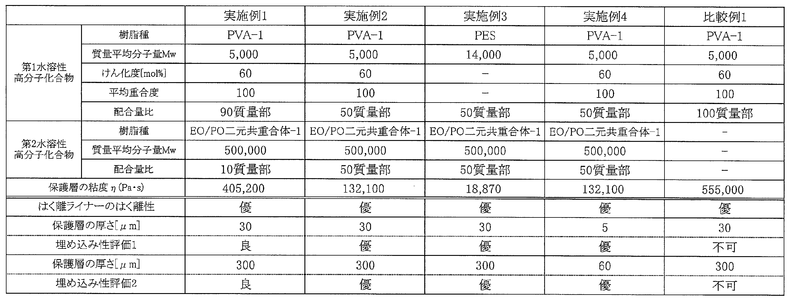
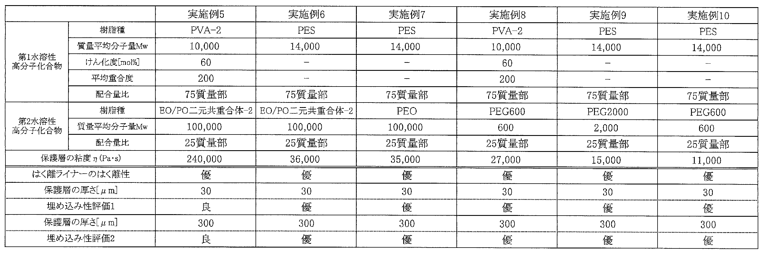
これに対し、比較例に係る保護シートでは、埋め込み性の評価1の結果、及び、評価2の結果がいずれも「不可」であった。
上記の結果から把握されるように、本実施形態に係る保護シートを用いることで、半導体ウエハの一方の面に設けられた電極部を保護層の内部に十分に埋設させることができる。
従って、本実施形態に係る保護シートを用いて半導体ウエハに対してバックグラインド加工するときに、半導体ウエハが備える半導体ウエハ本体に厚さのばらつきが生じることを抑制できると考えられる。
なお、上記の「はく離ライナーのはく離性の評価」を実施した評価結果は、いずれも「優」であった。
また、被着体であるシリコンウエハ(保護対象面)における縁と、保護層の縁とが重なるように保護対象面に保護層を貼り合わせ、保護層が縁からはみ出すか否かを観察した。その結果、実施例8乃至10の各保護層でははみ出しが観察されたが、その他の保護層でははみ出しが観察されなかった。
質量比率がPVA:EO/PO二元共重合体=5:95となるように、PVAとEO/PO二元共重合体とを水に分散させて水分散液を調製した。PVAとして上記の「PVA-1」を使用し、EO/PO二元共重合体として上記の「EO/PO共重合体-1」を使用した。その後、実施例1と同様にして、保護層形成用組成物を得た。
次に、実施例1と同様にして、PETはく離ライナー上に厚さ30μmの保護層を形成した。すなわち、PETはく離ライナー、厚さ30μmの保護層、及び、PETはく離ライナーがこの順で積層された保護シートを得た。
別途、実施例1と同様にして、PETはく離ライナー上に厚さ300μmの保護層を形成した。すなわち、PETはく離ライナー、厚さ300μmの保護層、及び、PETはく離ライナーがこの順で積層された保護シートをさらに得た。
また、参考例の保護シート(保護層の厚さが300μm)について、上記の方法と同様の方法によって、埋め込み性の評価2を実施した。結果を表3に示す。
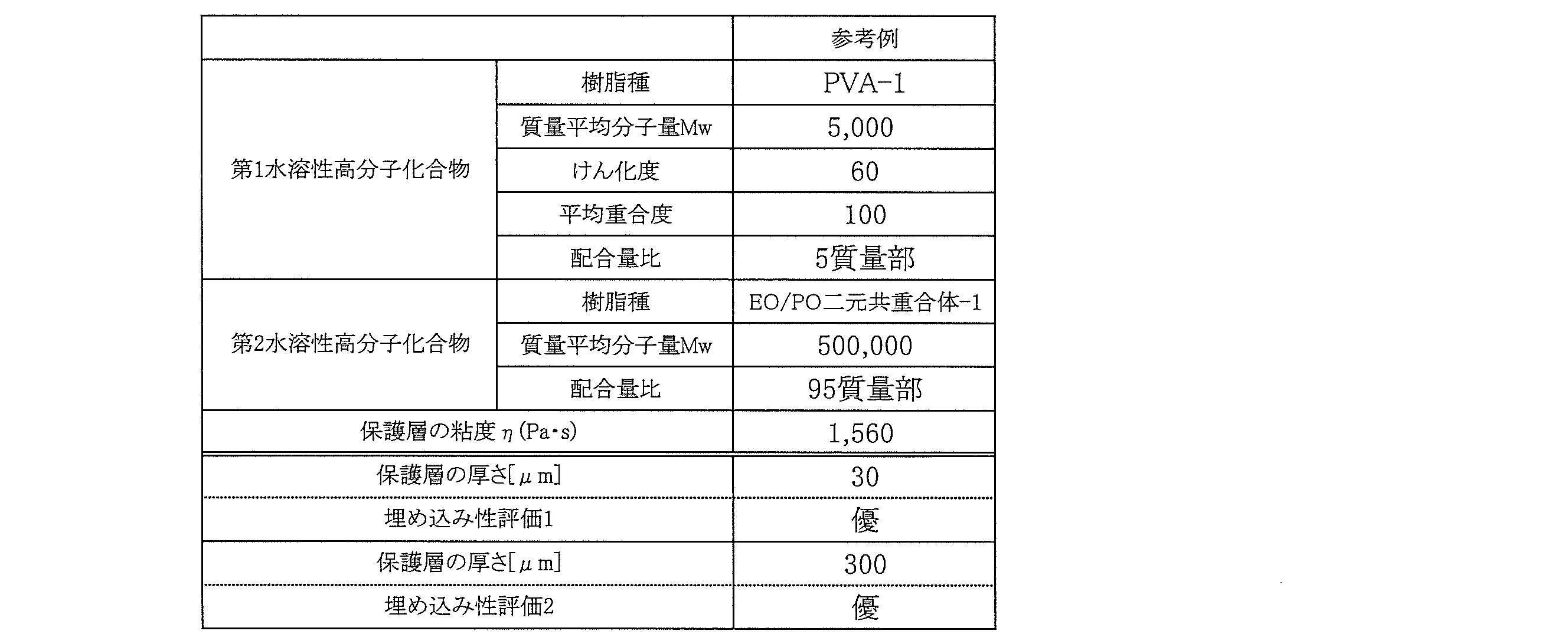
10a:保護層、 10b:基材層、 10c:粘着剤層、 10d:第1はく離ライナー、 10e:第2はく離ライナー、
20:半導体ウエハ、
20a:半導体ウエハ本体、 20b:電極部、 20b1:バンプ電極、
20’:半導体チップ、
100:ウエハレベルパッケージ、 110:回路基板、 120:半導体パッケージ、
120a:ガラス片、
200:イメージセンサパッケージ、 210:センサチップ本体、 220:接着層、 230:ガラス片、
200’:イメージセンサパッケージ用積層体、 210’:センサウエハ本体、 220’:接着層、 230’:ガラス板、
300:バックグラインド装置、 310:吸着プレート、 320:研磨ヘッド、
320a:研磨ヘッド本体、 320b:砥粒、
400:ブレードダイシング装置、
DB:ダイシングブレード、 SP:液体噴霧部、 ST:ステージ。
Claims (4)
- 電子部品の保護対象面、又は、前記電子部品の複数が連結された電子部品連結体の保護対象面に被着されて用いられる保護層を備え、
前記保護層が、水溶性高分子化合物を含み、
前記保護層の粘度ηが、60℃において50万Pa・s以下である、保護シート。 - 前記保護層は、前記水溶性高分子化合物として、第1水溶性高分子化合物と、該第1水溶性高分子化合物よりも質量平均分子量が大きい第2水溶性高分子化合物とを含み、
ゲルパーミエーションクロマトグラフィ測定に基づく質量分子量分布のピーク解析において、前記第1水溶性高分子化合物の質量平均分子量のピークトップが1000以上2万以下の範囲内に存在し、前記第2水溶性高分子化合物の質量平均分子量のピークトップが10万以上100万以下の範囲内に存在する、請求項1に記載の保護シート。 - 電子部品の保護対象面、又は、前記電子部品の複数が連結された電子部品連結体の保護対象面に被着されて用いられる保護層を備え、
前記保護層が、ポリビニルアルコールおよび水溶性ポリエステルのうち少なくとも一方と、エチレンオキシドに由来する構成単位を有する重合体と、を水溶性高分子化合物として含む、保護シート。 - 前記保護層の一方の面と対向するように配された基材層と、
前記保護層と前記基材層との間に配された粘着剤層と、を備え、
前記粘着剤層の両面が、前記保護層及び前記基材層にそれぞれ剥離可能に粘着している、請求項1乃至3のいずれか1項に記載の保護シート。
Priority Applications (3)
| Application Number | Priority Date | Filing Date | Title |
|---|---|---|---|
| KR1020257031447A KR20260025291A (ko) | 2023-06-16 | 2024-06-14 | 보호 시트 |
| JP2025528005A JP7808237B2 (ja) | 2023-06-16 | 2024-06-14 | 保護シート |
| CN202480037764.XA CN121311561A (zh) | 2023-06-16 | 2024-06-14 | 保护片 |
Applications Claiming Priority (4)
| Application Number | Priority Date | Filing Date | Title |
|---|---|---|---|
| JP2023099188 | 2023-06-16 | ||
| JP2023-099188 | 2023-06-16 | ||
| JP2023-214696 | 2023-12-20 | ||
| JP2023214696 | 2023-12-20 |
Publications (1)
| Publication Number | Publication Date |
|---|---|
| WO2024257849A1 true WO2024257849A1 (ja) | 2024-12-19 |
Family
ID=93852215
Family Applications (1)
| Application Number | Title | Priority Date | Filing Date |
|---|---|---|---|
| PCT/JP2024/021638 Ceased WO2024257849A1 (ja) | 2023-06-16 | 2024-06-14 | 保護シート |
Country Status (5)
| Country | Link |
|---|---|
| JP (1) | JP7808237B2 (ja) |
| KR (1) | KR20260025291A (ja) |
| CN (1) | CN121311561A (ja) |
| TW (1) | TWI926319B (ja) |
| WO (1) | WO2024257849A1 (ja) |
Citations (4)
| Publication number | Priority date | Publication date | Assignee | Title |
|---|---|---|---|---|
| JPH08253757A (ja) * | 1995-03-17 | 1996-10-01 | Sekisui Chem Co Ltd | 水溶性粘着剤組成物及びマスキング用水溶性粘着テープ |
| JP2004253612A (ja) * | 2003-02-20 | 2004-09-09 | Nitto Denko Corp | 半導体ウエハの仮固定方法及び電子部品、回路基板 |
| WO2019176554A1 (ja) * | 2018-03-14 | 2019-09-19 | デクセリアルズ株式会社 | アンダーフィル材、及びこれを用いた半導体装置の製造方法 |
| JP2022546761A (ja) * | 2019-09-06 | 2022-11-08 | スマートメディクス エスピー. ゼット オー. オー. | 局所リザーバを備えた層構造 |
Family Cites Families (2)
| Publication number | Priority date | Publication date | Assignee | Title |
|---|---|---|---|---|
| WO2016063917A1 (ja) * | 2014-10-23 | 2016-04-28 | リンテック株式会社 | 表面保護用シート |
| KR102510144B1 (ko) * | 2015-01-30 | 2023-03-14 | 린텍 가부시키가이샤 | 반도체 가공용 점착 시트 |
-
2024
- 2024-06-13 TW TW113121793A patent/TWI926319B/zh active
- 2024-06-14 CN CN202480037764.XA patent/CN121311561A/zh active Pending
- 2024-06-14 JP JP2025528005A patent/JP7808237B2/ja active Active
- 2024-06-14 KR KR1020257031447A patent/KR20260025291A/ko active Pending
- 2024-06-14 WO PCT/JP2024/021638 patent/WO2024257849A1/ja not_active Ceased
Patent Citations (4)
| Publication number | Priority date | Publication date | Assignee | Title |
|---|---|---|---|---|
| JPH08253757A (ja) * | 1995-03-17 | 1996-10-01 | Sekisui Chem Co Ltd | 水溶性粘着剤組成物及びマスキング用水溶性粘着テープ |
| JP2004253612A (ja) * | 2003-02-20 | 2004-09-09 | Nitto Denko Corp | 半導体ウエハの仮固定方法及び電子部品、回路基板 |
| WO2019176554A1 (ja) * | 2018-03-14 | 2019-09-19 | デクセリアルズ株式会社 | アンダーフィル材、及びこれを用いた半導体装置の製造方法 |
| JP2022546761A (ja) * | 2019-09-06 | 2022-11-08 | スマートメディクス エスピー. ゼット オー. オー. | 局所リザーバを備えた層構造 |
Also Published As
| Publication number | Publication date |
|---|---|
| TW202517745A (zh) | 2025-05-01 |
| TWI926319B (zh) | 2026-05-21 |
| CN121311561A (zh) | 2026-01-09 |
| JPWO2024257849A1 (ja) | 2024-12-19 |
| JP7808237B2 (ja) | 2026-01-28 |
| KR20260025291A (ko) | 2026-02-24 |
Similar Documents
| Publication | Publication Date | Title |
|---|---|---|
| US10699933B2 (en) | Wafer-fixing tape, method of processing a semiconductor wafer, and semiconductor chip | |
| KR102042598B1 (ko) | 표면 보호 시트 | |
| TWI814821B (zh) | 切晶黏晶膜及半導體裝置製造方法 | |
| CN100334690C (zh) | 半导体晶片表面保护用粘结膜及用该粘结膜的半导体晶片的保护方法 | |
| TW201942969A (zh) | 半導體晶片之製造方法、表面保護膠帶 | |
| US11056388B2 (en) | Mask-integrated surface protective tape | |
| US10971387B2 (en) | Mask-integrated surface protective tape | |
| JP4674836B2 (ja) | ダイシング用粘着シート | |
| KR20150113829A (ko) | 다이 본드 필름, 다이싱·다이 본드 필름 및 적층 필름 | |
| US20180226359A1 (en) | Mask-integrated surface protective tape | |
| KR101766174B1 (ko) | 반도체 웨이퍼 가공용 점착 테이프 및 반도체 웨이퍼의 가공 방법 | |
| EP3605586A1 (en) | Mask-integrated surface protective tape with release liner | |
| KR20180116751A (ko) | 다이싱 다이 본드 필름 | |
| JP7807971B2 (ja) | 電子部品装置の製造方法 | |
| JP2024135137A (ja) | 保護シート、及び、電子部品装置の製造方法 | |
| WO2023058481A1 (ja) | 電子部品装置の製造方法 | |
| CN111009488A (zh) | 切割芯片接合薄膜 | |
| JP7808237B2 (ja) | 保護シート | |
| JP2023043723A (ja) | 半導体加工用テープ、及び半導体チップの製造方法 | |
| JP7731412B2 (ja) | 保護シート、及び、電子部品装置の製造方法 | |
| JP7802816B2 (ja) | 保護シート、電子部品の製造方法、及び、表示装置の表示面を構成するガラス片の製造方法 | |
| JP2025068533A (ja) | ダイボンドフィルム及びダイシングダイボンドフィルム | |
| KR20240005907A (ko) | 백그라인드용 점착성 필름 및 전자 장치의 제조 방법 | |
| WO2026105568A1 (ja) | 半導体加工用シート | |
| KR20240005908A (ko) | 전자 장치의 제조 방법 |
Legal Events
| Date | Code | Title | Description |
|---|---|---|---|
| 121 | Ep: the epo has been informed by wipo that ep was designated in this application |
Ref document number: 24823462 Country of ref document: EP Kind code of ref document: A1 |
|
| ENP | Entry into the national phase |
Ref document number: 2025528005 Country of ref document: JP Kind code of ref document: A |
|
| WWE | Wipo information: entry into national phase |
Ref document number: 2025528005 Country of ref document: JP |
|
| NENP | Non-entry into the national phase |
Ref country code: DE |
|
| 122 | Ep: pct application non-entry in european phase |
Ref document number: 24823462 Country of ref document: EP Kind code of ref document: A1 |